EP0068012B1 - Photomasque et procede de fabrication - Google Patents
Photomasque et procede de fabrication Download PDFInfo
- Publication number
- EP0068012B1 EP0068012B1 EP82900445A EP82900445A EP0068012B1 EP 0068012 B1 EP0068012 B1 EP 0068012B1 EP 82900445 A EP82900445 A EP 82900445A EP 82900445 A EP82900445 A EP 82900445A EP 0068012 B1 EP0068012 B1 EP 0068012B1
- Authority
- EP
- European Patent Office
- Prior art keywords
- coverplate
- baseplate
- photomask
- liquid
- transparent
- Prior art date
- Legal status (The legal status is an assumption and is not a legal conclusion. Google has not performed a legal analysis and makes no representation as to the accuracy of the status listed.)
- Expired
Links
Images
Classifications
-
- G—PHYSICS
- G03—PHOTOGRAPHY; CINEMATOGRAPHY; ANALOGOUS TECHNIQUES USING WAVES OTHER THAN OPTICAL WAVES; ELECTROGRAPHY; HOLOGRAPHY
- G03F—PHOTOMECHANICAL PRODUCTION OF TEXTURED OR PATTERNED SURFACES, e.g. FOR PRINTING, FOR PROCESSING OF SEMICONDUCTOR DEVICES; MATERIALS THEREFOR; ORIGINALS THEREFOR; APPARATUS SPECIALLY ADAPTED THEREFOR
- G03F1/00—Originals for photomechanical production of textured or patterned surfaces, e.g., masks, photo-masks, reticles; Mask blanks or pellicles therefor; Containers specially adapted therefor; Preparation thereof
- G03F1/38—Masks having auxiliary features, e.g. special coatings or marks for alignment or testing; Preparation thereof
- G03F1/48—Protective coatings
-
- Y—GENERAL TAGGING OF NEW TECHNOLOGICAL DEVELOPMENTS; GENERAL TAGGING OF CROSS-SECTIONAL TECHNOLOGIES SPANNING OVER SEVERAL SECTIONS OF THE IPC; TECHNICAL SUBJECTS COVERED BY FORMER USPC CROSS-REFERENCE ART COLLECTIONS [XRACs] AND DIGESTS
- Y10—TECHNICAL SUBJECTS COVERED BY FORMER USPC
- Y10T—TECHNICAL SUBJECTS COVERED BY FORMER US CLASSIFICATION
- Y10T428/00—Stock material or miscellaneous articles
- Y10T428/24—Structurally defined web or sheet [e.g., overall dimension, etc.]
- Y10T428/24802—Discontinuous or differential coating, impregnation or bond [e.g., artwork, printing, retouched photograph, etc.]
- Y10T428/24851—Intermediate layer is discontinuous or differential
- Y10T428/24868—Translucent outer layer
-
- Y—GENERAL TAGGING OF NEW TECHNOLOGICAL DEVELOPMENTS; GENERAL TAGGING OF CROSS-SECTIONAL TECHNOLOGIES SPANNING OVER SEVERAL SECTIONS OF THE IPC; TECHNICAL SUBJECTS COVERED BY FORMER USPC CROSS-REFERENCE ART COLLECTIONS [XRACs] AND DIGESTS
- Y10—TECHNICAL SUBJECTS COVERED BY FORMER USPC
- Y10T—TECHNICAL SUBJECTS COVERED BY FORMER US CLASSIFICATION
- Y10T428/00—Stock material or miscellaneous articles
- Y10T428/24—Structurally defined web or sheet [e.g., overall dimension, etc.]
- Y10T428/24802—Discontinuous or differential coating, impregnation or bond [e.g., artwork, printing, retouched photograph, etc.]
- Y10T428/24917—Discontinuous or differential coating, impregnation or bond [e.g., artwork, printing, retouched photograph, etc.] including metal layer
-
- Y—GENERAL TAGGING OF NEW TECHNOLOGICAL DEVELOPMENTS; GENERAL TAGGING OF CROSS-SECTIONAL TECHNOLOGIES SPANNING OVER SEVERAL SECTIONS OF THE IPC; TECHNICAL SUBJECTS COVERED BY FORMER USPC CROSS-REFERENCE ART COLLECTIONS [XRACs] AND DIGESTS
- Y10—TECHNICAL SUBJECTS COVERED BY FORMER USPC
- Y10T—TECHNICAL SUBJECTS COVERED BY FORMER US CLASSIFICATION
- Y10T428/00—Stock material or miscellaneous articles
- Y10T428/24—Structurally defined web or sheet [e.g., overall dimension, etc.]
- Y10T428/24802—Discontinuous or differential coating, impregnation or bond [e.g., artwork, printing, retouched photograph, etc.]
- Y10T428/24926—Discontinuous or differential coating, impregnation or bond [e.g., artwork, printing, retouched photograph, etc.] including ceramic, glass, porcelain or quartz layer
-
- Y—GENERAL TAGGING OF NEW TECHNOLOGICAL DEVELOPMENTS; GENERAL TAGGING OF CROSS-SECTIONAL TECHNOLOGIES SPANNING OVER SEVERAL SECTIONS OF THE IPC; TECHNICAL SUBJECTS COVERED BY FORMER USPC CROSS-REFERENCE ART COLLECTIONS [XRACs] AND DIGESTS
- Y10—TECHNICAL SUBJECTS COVERED BY FORMER USPC
- Y10T—TECHNICAL SUBJECTS COVERED BY FORMER US CLASSIFICATION
- Y10T428/00—Stock material or miscellaneous articles
- Y10T428/31—Surface property or characteristic of web, sheet or block
Definitions
- the instant invention relates to integrated circuit photomasks.
- the invention is directed to photomasks, techniques for manufacturing same, and for methods of using such masks in projection printing.
- Photomasks used for projection printing wherein the photomask is spaced from a resist coated semiconductor wafer or the like, have high resolution metallic patterns on glass substrates, with feature sizes approaching the 1 um-2 pm range.
- the quality of the pattern is very critical to the semiconductor manufacturing process, thus, care is taken to fabricate such photomasks substantially free of any defects.
- Maintaining the photomasks in this defect free state is essential if acceptable device yields are to be obtained.
- the various cleaning and handling operations that the photomask is subjected to can cause a slow deterioration of the pattern.
- the yield loss can become significant. For these reasons it is economically desirable to find a method whereby the mask surface can be protected from both contamination and deterioration while maintaining acceptable resolution.
- German Patent DE-B-2,845,147 discloses a mask for a projection system, the mask comprising a baseplate having a mask pattern thereon and a coverplate overlying the mask pattern with a layer of Canada Balsam optical cement between the coverplate and the baseplate.
- the mask was designed for a 5 to 1 image projection system. Systems which achieve 5 to 1 projection of images have a much greater depth of focus than a system which achieves a 1 to 1 projection of images.
- the prior art cover plate Used in the mask of the 5 to 1 projection system can be relatively thick (namely 0.229 cms). It was not considered to be too significant a problem to machine such a relatively thick plate to a high degree of accuracy, although with the 5 to 1 projection system, the latter would not suffer loss of focus if the thickness variation of the coverplate were substantially greater than 15 pm.
- a photomask for use with a projection printer system comprising a transparent baseplate with metallized and unmetallized portions on a major surface thereof, a transparent coverplate having parallel major surfaces with one major surface in intimate contact with the said metallized portions, and transparent material interposed between the baseplate and the said one major surface of the coverplate, the said material having an index of refraction substantially equal to that of the baseplate and/or coverplate characterised in that the coverplate (33) has a thickness of between 0.1023 cm and 0.0997 cm which thickness varies by 4 pm or less, and the said material is in bubble free and particle free liquid form.
- the instant mask has a longer life than prior art masks and only minor cleaning is required.
- the instant method of selectively exposing photoresist coated substrates has unexpectedly resulted in enhanced edge definition and virtually defect-free patterns in the photoresist.
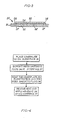
- a light projection system generally indicated by the numeral 10 in Fig. 1 has been used.
- a semiconductor wafer 11 having a resist coating (not shown) is vertically aligned with an ultraviolet source 12 and focusing optics.
- Such a projection system 10 is manufactured by the Perking-Elmer Company, as their "Microline” (Registered Trade Mark) Model No. 240.
- a photomask 16 is interposed between the ultraviolet source 12 and the focusing optics 13.
- the photomask 16 is comprised of a transparent substrate 17 such as fused silica with a metallic pattern 18 thereon.
- the ultraviolet radiation from the source 12 passes through the unmetallized areas 19 on the photomask 16 and is focused onto the resist coating on the semiconductor wafer 11 to expose the insolubilize (i.e. when using a negative acting resist) the resist coating.
- a suitable solvent is then employed to wash away the soluble resist coating in order that the exposed areas be further processed.
- Such a procedure is usually repeated a number of times using a plurality of photomasks 16 having different patterns 18 thereon to fabricate the desired circuits.
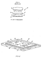
- a photomask 30 for use with a 1 to 1 projection system.
- the photomask 30 is comprised of a transparent baseplate 31 having a metallic pattern 32 thereon.
- a substantially flat, transparent, coverplate 33 is placed over the substrate 31.
- the coverplate 33 has a thickness of between 0.1023 cm and 0.0997 cm, which thickness varies by 4 um or less.
- an index matching liquid 34 (See Fig. 3) fills in the unmetallized volume between the baseplate 31 and the coverplate 33 to substantially eliminate interference fringes produced by light reflecting from the two surfaces in near contact. Bonding material 36 at the interface edge 37 between the baseplate 31 and the coverplate 33 holds the coverplate in place on the baseplate while sealing the index matching liquid 34 therein.
- the coverplate 33 and the baseplate 31 are both made of the same light transmissive material, and the index matching liquid 34 should have an index of refraction substantially equal to the materials from which the baseplate and coverplate are made.
- the index matching liquid 34 has substantially the same index of refraction as the coverplate 33.
- the metal used to form the pattern 32 was chrome.
- the index matching liquid 34 was composed of an aliphatic hydrocarbon hydrogenated terphenyl, type AA phthalate ester manufactured by R. P. Cargille Laboratories, Inc.
- the photomask 30 not only has a longer life expectancy but requires only minor cleaning and less frequent reinspection. In addition deterioration of the metallic pattern on the photomask due to electrostatic arcing between portions of the pattern is eliminated. Unexpectedly, the instant technique provides enhanced edge definition in the photoresist. Although the reason for such unexpected results are not clear it is suggested that the index matching liquid fills in the relatively rough portions of the glass substrate formed when the metallic pattern is fabricated by well known etching processes. Accordingly, the effective elimination of such a rough surface substantially decreases scattering of the light passing therethrough which heretofore caused a slight blurring of the image.
- the instant invention also contemplates the use of a mask wherein a thin layer of index matching liquid, having the same index of refraction as the baseplate, is deposited on at least the unmetallized surface thereof.
- the material may be applied by spraying, vapor deposition or the like depending upon the composition of the index matching liquid the metal used to form the pattern and the composition of the baseplate.
- coverplate 33 to the baseplate 31 in a projection printer system 10 (Fig. 1) requires certain adjustments due to effects on both first and third order aberrations of the optical system.
- the first-order effect of the glass coverplate 33 is to move the paraxial image plane by an amount Af given by
- t an n' are the thickness and the index of refraction of the coverplate 33 respectively.
- This shift is taken into account by refocusing the printer.
- the size of the focal shift is also important in tolerancing the thickness of the coverplate 33.
- the required tolerance is much tighter since allowance must be made for flatness variation of the coated semiconductor wafer 11.
- the distance between the coverplate 33 and the baseplate 31 surface should be as uniform as practicable.
- the primary higher order aberration introduced by the addition of the coverplate 33 is spherical aberration.
- Ray tracing shows this contribution to be quite small for an optical system with a numerical aperture of 0.1667 such as the particular printer used.
- the spot size due to spherical aberration is 0.1 pm at best focus and with a 1.0 mm coverplate 33 the spot size is 0.2 ⁇ m. These spot sizes are small when compared with the diffraction limited spot size of 1.25 pm.
- the spherical aberration also causes a shift in the optimal focal plane away from the paraxial focal plane, causing a shortening of the back focal distance.
- the only other effect attributable to the coverplate 33 is a slight reduction in the projected image contrast. This results from the light reflected from the face of the coverplate 33 and illuminating the chrome pattern 32. Without the cover plate 33 the contrast of the chrome on glass pattern 32 is 100%. If there is a 4% reflection from the surface of the coverplate 33 and 100% reflection from the chrome then the contrast is reduced to no less than 92%. Because of the high contrast of the photoresist this contrast reduction does not seriously effect the printing process.
- the coverglass 33 was fabricated by initialling selecting a substantially defect-free fused quartz plate having dimensions of approximately 11.1 cm.x11.4 cm.x0.16 cm.
- the plate was then wax mounted to the surface of a support member that has a flatness of 1/4 ⁇ .
- the mounted plate is then lapped and polished to within 1 pm.
- the plate was then removed from the flat support member, turned, over, and mounted on a 1/4 A optical flat with intimate contact therebetween.
- An RTV silicone rubber adhesive was deposited at the edges of the plate to bond the plate to the optical flat.
- the plate is again lapped and polished until the plate has a thickness of 0.101 cm ⁇ 0.0013 cm (i.e.
- the photomask 30 be assembled in a "clean room” environment to ensure a defect-free baseplate 31-coverplate 33 interface.
- the index matching liquid 34 is sequentially filtered through two "Millipore” (Registered Trade Mark) GVHP 02500 0.2 p filters and outgassed in a rough vacuum for approximately four hours to remove any dissolved gases therein and the baseplate 31 and the coverplate 33 are cleaned and dried.
- the coverplate 33 is then placed on the baseplated 31 (see Figs. 2 and 3) and lightly pressed to remove any trapped air therebetween.
- the four corners of the coverplate 33 are then tack bonded to the base plate 31 using an epoxy adhesive.
- the adhesive should be allowed to dry thoroughly.
- the resulting assembly is then heated to approximately 70°C and one or more drops of the index matching liquid 34 deposited at the interface edge 37 at one side of the coverplate 33.
- the liquid 34 will also be heated and be drawn between the coverplate 33 and the baseplate 31 by capillary action to fill the unpatterned volume therebetween as well as to form a thin layer of liquid between the metallic pattern 32 and the coverplate. Additional liquid 34 may be added as necessary as required to fill the volume between the coverplate 33 and the baseplate 31. To ensure that the volume vs completely filled the assembly may heat overnight (e.g., approximately 15 hours) at 70°C.
- a small pool of the index matching liquid 34 is deposited on the central portion of the baseplate 31 or the coverplate 33 prior to placing them into intimate contact.
- the liquid 34 is then heated to approximately 70 to 100°C for several hours to fill, in between the baseplate 31 and the coverplate 33. Again, a thin film of the liquid 34 will remain between the surface of the metallic pattern 32 and the coverplate 33. If gas bubbles form between the baseplate 31 and the coverplate 33 they should be worked out by selectively applying pressure. Once all bubbles are removed the interface may be sealed as hereinbefore described.
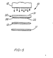
- FIG. 5 An exemplary embodiment of a light projection system 10, implemented using the instant techniques, is shown in Fig. 5.
- the photomash 30, shown in detail in Fig. 3, is positioned between the ultraviolet light source 12 and a photoresist, coated substrate 11.
- Focusing optics 13 are positioned in spaced relation to the substrate 11.
- the light source 12 is activated to direct light radiation through the patterned photomask 30 to selectively expose the photoresist coated substrate 11 thereto.
- Such a projection printing method has resulted in an enhanced edge definition and virtually defect-free patterns in the photoresist.
Landscapes
- Physics & Mathematics (AREA)
- General Physics & Mathematics (AREA)
- Exposure And Positioning Against Photoresist Photosensitive Materials (AREA)
Claims (6)
Applications Claiming Priority (4)
| Application Number | Priority Date | Filing Date | Title |
|---|---|---|---|
| US22245181A | 1981-01-05 | 1981-01-05 | |
| US222451 | 1981-01-05 | ||
| US06/287,970 US4361643A (en) | 1981-01-05 | 1981-07-29 | Photomask and method of using same |
| US287970 | 1988-12-21 |
Publications (3)
| Publication Number | Publication Date |
|---|---|
| EP0068012A1 EP0068012A1 (fr) | 1983-01-05 |
| EP0068012A4 EP0068012A4 (fr) | 1983-07-04 |
| EP0068012B1 true EP0068012B1 (fr) | 1986-04-23 |
Family
ID=26916806
Family Applications (1)
| Application Number | Title | Priority Date | Filing Date |
|---|---|---|---|
| EP82900445A Expired EP0068012B1 (fr) | 1981-01-05 | 1981-12-17 | Photomasque et procede de fabrication |
Country Status (5)
| Country | Link |
|---|---|
| US (1) | US4361643A (fr) |
| EP (1) | EP0068012B1 (fr) |
| GB (1) | GB2092773B (fr) |
| IT (1) | IT1140429B (fr) |
| WO (1) | WO1982002361A1 (fr) |
Families Citing this family (7)
| Publication number | Priority date | Publication date | Assignee | Title |
|---|---|---|---|---|
| US4537813A (en) * | 1982-09-27 | 1985-08-27 | At&T Technologies, Inc. | Photomask encapsulation |
| US4499162A (en) * | 1983-06-24 | 1985-02-12 | At&T Technologies, Inc. | Photomask and method of using same |
| US4529299A (en) * | 1984-05-03 | 1985-07-16 | At&T Technologies, Inc. | Interposer element for photomasks in projection printer |
| US4537498A (en) * | 1984-05-03 | 1985-08-27 | At&T Technologies, Inc. | Focal plane adjusted photomask and methods of projecting images onto photosensitized workpiece surfaces |
| US4915058A (en) * | 1988-11-21 | 1990-04-10 | Murray Douglas A | Window mask with releasable securing means |
| US5076654A (en) * | 1990-10-29 | 1991-12-31 | At&T Bell Laboratories | Packaging of silicon optical components |
| US5656093A (en) * | 1996-03-08 | 1997-08-12 | Applied Materials, Inc. | Wafer spacing mask for a substrate support chuck and method of fabricating same |
Family Cites Families (12)
| Publication number | Priority date | Publication date | Assignee | Title |
|---|---|---|---|---|
| US1985074A (en) * | 1932-11-02 | 1934-12-18 | Zeiss Carl | Illumination system |
| US2175343A (en) * | 1937-09-24 | 1939-10-10 | Radio Keith Orpheum Corp | Plate cooler for stereopticon slides |
| US2317550A (en) * | 1941-06-17 | 1943-04-27 | Joseph D Ramsey | Projection device |
| US3193840A (en) * | 1961-10-27 | 1965-07-06 | Raymond C Mercer | Apparatus for liquid immersion motion picture film projection |
| US3400995A (en) * | 1965-12-09 | 1968-09-10 | Gen Precision Systems Inc | Heat dissipating film gate |
| FR1594635A (fr) * | 1967-10-17 | 1970-06-08 | ||
| NL6814882A (fr) * | 1967-12-12 | 1969-06-16 | ||
| US3906133A (en) * | 1974-04-23 | 1975-09-16 | Harris Corp | Nitrocellulose protective coating on masks used in IC manufacture |
| FR2280924A1 (fr) * | 1974-08-02 | 1976-02-27 | Silec Semi Conducteurs | Procede de protection de masques de photogravure et masques obtenus |
| US4201581A (en) * | 1978-03-13 | 1980-05-06 | Eastman Kodak Company | Method of providing close contact for contact printing |
| US4256787A (en) * | 1978-05-03 | 1981-03-17 | Massachusetts Institute Of Technology | Orientation of ordered liquids and their use in devices |
| DE2845147B1 (de) * | 1978-10-17 | 1980-01-17 | Censor Patent Versuch | Projektionsmaske |
-
1981
- 1981-07-29 US US06/287,970 patent/US4361643A/en not_active Expired - Lifetime
- 1981-12-17 EP EP82900445A patent/EP0068012B1/fr not_active Expired
- 1981-12-17 WO PCT/US1981/001681 patent/WO1982002361A1/fr active IP Right Grant
- 1981-12-30 GB GB8139104A patent/GB2092773B/en not_active Expired
- 1981-12-30 IT IT25925/81A patent/IT1140429B/it active
Non-Patent Citations (1)
| Title |
|---|
| IBM TECHNICAL DISCLOSURE BULLETIN, vol. 14, no. 1, June 1971, NEW YORK (US) J. SYBALSKY: "Protective coating for resist-coated chrome over glass masks", page 249 * |
Also Published As
| Publication number | Publication date |
|---|---|
| GB2092773B (en) | 1985-06-05 |
| US4361643A (en) | 1982-11-30 |
| GB2092773A (en) | 1982-08-18 |
| EP0068012A1 (fr) | 1983-01-05 |
| IT1140429B (it) | 1986-09-24 |
| EP0068012A4 (fr) | 1983-07-04 |
| WO1982002361A1 (fr) | 1982-07-22 |
| IT8125925A0 (it) | 1981-12-30 |
Similar Documents
| Publication | Publication Date | Title |
|---|---|---|
| US4405701A (en) | Methods of fabricating a photomask | |
| US4131363A (en) | Pellicle cover for projection printing system | |
| US4833051A (en) | Protective device for photographic masks | |
| US6562523B1 (en) | Direct write all-glass photomask blanks | |
| US4063812A (en) | Projection printing system with an improved mask configuration | |
| US4537813A (en) | Photomask encapsulation | |
| EP0068012B1 (fr) | Photomasque et procede de fabrication | |
| US6317197B1 (en) | Mask pellicle remove tool | |
| US6317274B1 (en) | Optical element | |
| EP0119310B1 (fr) | Procédé pour la fabrication d'un opercule pelliculaire pour un système d'exposition par projection | |
| US4499162A (en) | Photomask and method of using same | |
| US3507592A (en) | Method of fabricating photomasks | |
| US4523974A (en) | Method of fabricating a pellicle cover for projection printing system | |
| SU938338A1 (ru) | Фотошаблон и способ его изготовлени | |
| JPH0213780B2 (fr) | ||
| EP0179146B1 (fr) | Photomasque ajuste par rapport au plan focal et procedes de projection d'images sur des surfaces photosensibilisees a traiter | |
| KR20070051965A (ko) | 기판 노광 공정에 사용되는 레티클 | |
| EP0118623A1 (fr) | Opercule pelliculaire pour photomasque | |
| JPS6053871B2 (ja) | 露光方法 | |
| JPS6083019A (ja) | パタ−ン反射型投影露光方法 | |
| US7344807B2 (en) | Gassing-free exposure mask | |
| JPS6154211B2 (fr) | ||
| US6567153B1 (en) | Multiple image photolithography system and method | |
| JPH04204946A (ja) | 露光装置 | |
| JPS6231855A (ja) | ペリクル付マスクブランク |
Legal Events
| Date | Code | Title | Description |
|---|---|---|---|
| PUAI | Public reference made under article 153(3) epc to a published international application that has entered the european phase |
Free format text: ORIGINAL CODE: 0009012 |
|
| AK | Designated contracting states |
Designated state(s): CH DE FR LI NL |
|
| 17P | Request for examination filed |
Effective date: 19830113 |
|
| GRAA | (expected) grant |
Free format text: ORIGINAL CODE: 0009210 |
|
| AK | Designated contracting states |
Kind code of ref document: B1 Designated state(s): CH DE FR LI NL |
|
| REF | Corresponds to: |
Ref document number: 3174495 Country of ref document: DE Date of ref document: 19860528 |
|
| ET | Fr: translation filed | ||
| PLBE | No opposition filed within time limit |
Free format text: ORIGINAL CODE: 0009261 |
|
| STAA | Information on the status of an ep patent application or granted ep patent |
Free format text: STATUS: NO OPPOSITION FILED WITHIN TIME LIMIT |
|
| 26N | No opposition filed | ||
| PGFP | Annual fee paid to national office [announced via postgrant information from national office to epo] |
Ref country code: CH Payment date: 19990927 Year of fee payment: 19 |
|
| PGFP | Annual fee paid to national office [announced via postgrant information from national office to epo] |
Ref country code: FR Payment date: 19991124 Year of fee payment: 19 |
|
| PGFP | Annual fee paid to national office [announced via postgrant information from national office to epo] |
Ref country code: NL Payment date: 19991129 Year of fee payment: 19 |
|
| PGFP | Annual fee paid to national office [announced via postgrant information from national office to epo] |
Ref country code: DE Payment date: 19991231 Year of fee payment: 19 |
|
| PG25 | Lapsed in a contracting state [announced via postgrant information from national office to epo] |
Ref country code: LI Free format text: LAPSE BECAUSE OF NON-PAYMENT OF DUE FEES Effective date: 20001231 Ref country code: CH Free format text: LAPSE BECAUSE OF NON-PAYMENT OF DUE FEES Effective date: 20001231 |
|
| PG25 | Lapsed in a contracting state [announced via postgrant information from national office to epo] |
Ref country code: NL Free format text: LAPSE BECAUSE OF NON-PAYMENT OF DUE FEES Effective date: 20010701 |
|
| REG | Reference to a national code |
Ref country code: CH Ref legal event code: PL |
|
| PG25 | Lapsed in a contracting state [announced via postgrant information from national office to epo] |
Ref country code: FR Free format text: LAPSE BECAUSE OF NON-PAYMENT OF DUE FEES Effective date: 20010831 |
|
| NLV4 | Nl: lapsed or anulled due to non-payment of the annual fee |
Effective date: 20010701 |
|
| REG | Reference to a national code |
Ref country code: FR Ref legal event code: ST |
|
| PG25 | Lapsed in a contracting state [announced via postgrant information from national office to epo] |
Ref country code: DE Free format text: LAPSE BECAUSE OF NON-PAYMENT OF DUE FEES Effective date: 20011002 |