EP0052373B1 - Verfahren zur Herstellung einer Abtastnadel - Google Patents
Verfahren zur Herstellung einer Abtastnadel Download PDFInfo
- Publication number
- EP0052373B1 EP0052373B1 EP81109722A EP81109722A EP0052373B1 EP 0052373 B1 EP0052373 B1 EP 0052373B1 EP 81109722 A EP81109722 A EP 81109722A EP 81109722 A EP81109722 A EP 81109722A EP 0052373 B1 EP0052373 B1 EP 0052373B1
- Authority
- EP
- European Patent Office
- Prior art keywords
- stylus
- substrate
- electrode
- diamond
- conductive layer
- Prior art date
- Legal status (The legal status is an assumption and is not a legal conclusion. Google has not performed a legal analysis and makes no representation as to the accuracy of the status listed.)
- Expired
Links
- 238000004519 manufacturing process Methods 0.000 title claims description 14
- 239000000758 substrate Substances 0.000 claims description 62
- 229910003460 diamond Inorganic materials 0.000 claims description 49
- 239000010432 diamond Substances 0.000 claims description 49
- 238000000034 method Methods 0.000 claims description 23
- 239000001301 oxygen Substances 0.000 claims description 12
- 229910052760 oxygen Inorganic materials 0.000 claims description 12
- 238000007788 roughening Methods 0.000 claims description 12
- 238000010849 ion bombardment Methods 0.000 claims description 11
- -1 oxygen ions Chemical class 0.000 claims description 10
- 229910021332 silicide Inorganic materials 0.000 claims description 6
- QVGXLLKOCUKJST-UHFFFAOYSA-N atomic oxygen Chemical compound [O] QVGXLLKOCUKJST-UHFFFAOYSA-N 0.000 claims description 5
- 229910052719 titanium Inorganic materials 0.000 claims description 5
- 229910052804 chromium Inorganic materials 0.000 claims description 4
- 229910052735 hafnium Inorganic materials 0.000 claims description 4
- 229910052758 niobium Inorganic materials 0.000 claims description 4
- 229910001220 stainless steel Inorganic materials 0.000 claims description 4
- 229910052715 tantalum Inorganic materials 0.000 claims description 4
- 229910052721 tungsten Inorganic materials 0.000 claims description 4
- 229910052726 zirconium Inorganic materials 0.000 claims description 4
- 239000010935 stainless steel Substances 0.000 claims description 3
- 239000000126 substance Substances 0.000 claims description 2
- 229910000990 Ni alloy Inorganic materials 0.000 claims 1
- 238000007599 discharging Methods 0.000 claims 1
- 239000010410 layer Substances 0.000 description 35
- 229910052751 metal Inorganic materials 0.000 description 29
- 239000002184 metal Substances 0.000 description 29
- 238000004544 sputter deposition Methods 0.000 description 23
- 239000010408 film Substances 0.000 description 18
- 241001422033 Thestylus Species 0.000 description 16
- XKRFYHLGVUSROY-UHFFFAOYSA-N Argon Chemical compound [Ar] XKRFYHLGVUSROY-UHFFFAOYSA-N 0.000 description 14
- 239000007789 gas Substances 0.000 description 11
- 229910052786 argon Inorganic materials 0.000 description 8
- 239000010936 titanium Substances 0.000 description 7
- IJGRMHOSHXDMSA-UHFFFAOYSA-N Atomic nitrogen Chemical compound N#N IJGRMHOSHXDMSA-UHFFFAOYSA-N 0.000 description 6
- 238000000227 grinding Methods 0.000 description 6
- 150000002500 ions Chemical class 0.000 description 5
- 239000000463 material Substances 0.000 description 5
- 150000004767 nitrides Chemical class 0.000 description 5
- FVBUAEGBCNSCDD-UHFFFAOYSA-N silicide(4-) Chemical compound [Si-4] FVBUAEGBCNSCDD-UHFFFAOYSA-N 0.000 description 5
- 238000005530 etching Methods 0.000 description 4
- 229910052750 molybdenum Inorganic materials 0.000 description 4
- 238000000992 sputter etching Methods 0.000 description 4
- 229910001021 Ferroalloy Inorganic materials 0.000 description 3
- 229910004337 Ti-Ni Inorganic materials 0.000 description 3
- ATJFFYVFTNAWJD-UHFFFAOYSA-N Tin Chemical compound [Sn] ATJFFYVFTNAWJD-UHFFFAOYSA-N 0.000 description 3
- 229910011209 Ti—Ni Inorganic materials 0.000 description 3
- 229910045601 alloy Inorganic materials 0.000 description 3
- 239000000956 alloy Substances 0.000 description 3
- 238000005536 corrosion prevention Methods 0.000 description 3
- KHYBPSFKEHXSLX-UHFFFAOYSA-N iminotitanium Chemical compound [Ti]=N KHYBPSFKEHXSLX-UHFFFAOYSA-N 0.000 description 3
- 150000002739 metals Chemical class 0.000 description 3
- 229910052759 nickel Inorganic materials 0.000 description 3
- 229910052757 nitrogen Inorganic materials 0.000 description 3
- 238000005546 reactive sputtering Methods 0.000 description 3
- 229910016006 MoSi Inorganic materials 0.000 description 2
- BLRPTPMANUNPDV-UHFFFAOYSA-N Silane Chemical compound [SiH4] BLRPTPMANUNPDV-UHFFFAOYSA-N 0.000 description 2
- XUIMIQQOPSSXEZ-UHFFFAOYSA-N Silicon Chemical compound [Si] XUIMIQQOPSSXEZ-UHFFFAOYSA-N 0.000 description 2
- HSFWRNGVRCDJHI-UHFFFAOYSA-N alpha-acetylene Natural products C#C HSFWRNGVRCDJHI-UHFFFAOYSA-N 0.000 description 2
- 239000011248 coating agent Substances 0.000 description 2
- 238000000576 coating method Methods 0.000 description 2
- 239000004020 conductor Substances 0.000 description 2
- 238000010276 construction Methods 0.000 description 2
- 238000007796 conventional method Methods 0.000 description 2
- 238000010586 diagram Methods 0.000 description 2
- 238000009792 diffusion process Methods 0.000 description 2
- 230000000694 effects Effects 0.000 description 2
- 239000007772 electrode material Substances 0.000 description 2
- 125000002534 ethynyl group Chemical group [H]C#C* 0.000 description 2
- 238000002474 experimental method Methods 0.000 description 2
- 238000007730 finishing process Methods 0.000 description 2
- 239000003960 organic solvent Substances 0.000 description 2
- 238000011160 research Methods 0.000 description 2
- 238000007493 shaping process Methods 0.000 description 2
- 229910000077 silane Inorganic materials 0.000 description 2
- 229910052710 silicon Inorganic materials 0.000 description 2
- 239000010703 silicon Substances 0.000 description 2
- 239000002344 surface layer Substances 0.000 description 2
- 239000010409 thin film Substances 0.000 description 2
- 238000007740 vapor deposition Methods 0.000 description 2
- MYMOFIZGZYHOMD-UHFFFAOYSA-N Dioxygen Chemical compound O=O MYMOFIZGZYHOMD-UHFFFAOYSA-N 0.000 description 1
- 229910017305 Mo—Si Inorganic materials 0.000 description 1
- 239000004698 Polyethylene Substances 0.000 description 1
- 229910001069 Ti alloy Inorganic materials 0.000 description 1
- 239000002390 adhesive tape Substances 0.000 description 1
- 125000004432 carbon atom Chemical group C* 0.000 description 1
- 239000000919 ceramic Substances 0.000 description 1
- 238000004140 cleaning Methods 0.000 description 1
- 150000001875 compounds Chemical class 0.000 description 1
- 238000005520 cutting process Methods 0.000 description 1
- 230000007423 decrease Effects 0.000 description 1
- 230000003247 decreasing effect Effects 0.000 description 1
- 238000000151 deposition Methods 0.000 description 1
- 230000008021 deposition Effects 0.000 description 1
- 229910001882 dioxygen Inorganic materials 0.000 description 1
- 229920006332 epoxy adhesive Polymers 0.000 description 1
- 229910052737 gold Inorganic materials 0.000 description 1
- 238000010438 heat treatment Methods 0.000 description 1
- 239000011261 inert gas Substances 0.000 description 1
- 229910052741 iridium Inorganic materials 0.000 description 1
- 229910052743 krypton Inorganic materials 0.000 description 1
- DNNSSWSSYDEUBZ-UHFFFAOYSA-N krypton atom Chemical compound [Kr] DNNSSWSSYDEUBZ-UHFFFAOYSA-N 0.000 description 1
- 150000001247 metal acetylides Chemical class 0.000 description 1
- 229910000510 noble metal Inorganic materials 0.000 description 1
- 230000006911 nucleation Effects 0.000 description 1
- 238000010899 nucleation Methods 0.000 description 1
- 230000003287 optical effect Effects 0.000 description 1
- 150000002894 organic compounds Chemical class 0.000 description 1
- 230000010355 oscillation Effects 0.000 description 1
- 229910052697 platinum Inorganic materials 0.000 description 1
- 229920000573 polyethylene Polymers 0.000 description 1
- 239000000376 reactant Substances 0.000 description 1
- 229910052703 rhodium Inorganic materials 0.000 description 1
- 229910052594 sapphire Inorganic materials 0.000 description 1
- 239000010980 sapphire Substances 0.000 description 1
- 238000003860 storage Methods 0.000 description 1
- 238000012360 testing method Methods 0.000 description 1
Images

Classifications
-
- C—CHEMISTRY; METALLURGY
- C04—CEMENTS; CONCRETE; ARTIFICIAL STONE; CERAMICS; REFRACTORIES
- C04B—LIME, MAGNESIA; SLAG; CEMENTS; COMPOSITIONS THEREOF, e.g. MORTARS, CONCRETE OR LIKE BUILDING MATERIALS; ARTIFICIAL STONE; CERAMICS; REFRACTORIES; TREATMENT OF NATURAL STONE
- C04B41/00—After-treatment of mortars, concrete, artificial stone or ceramics; Treatment of natural stone
- C04B41/009—After-treatment of mortars, concrete, artificial stone or ceramics; Treatment of natural stone characterised by the material treated
-
- C—CHEMISTRY; METALLURGY
- C04—CEMENTS; CONCRETE; ARTIFICIAL STONE; CERAMICS; REFRACTORIES
- C04B—LIME, MAGNESIA; SLAG; CEMENTS; COMPOSITIONS THEREOF, e.g. MORTARS, CONCRETE OR LIKE BUILDING MATERIALS; ARTIFICIAL STONE; CERAMICS; REFRACTORIES; TREATMENT OF NATURAL STONE
- C04B41/00—After-treatment of mortars, concrete, artificial stone or ceramics; Treatment of natural stone
- C04B41/0027—Ion-implantation, ion-irradiation or ion-injection
-
- C—CHEMISTRY; METALLURGY
- C04—CEMENTS; CONCRETE; ARTIFICIAL STONE; CERAMICS; REFRACTORIES
- C04B—LIME, MAGNESIA; SLAG; CEMENTS; COMPOSITIONS THEREOF, e.g. MORTARS, CONCRETE OR LIKE BUILDING MATERIALS; ARTIFICIAL STONE; CERAMICS; REFRACTORIES; TREATMENT OF NATURAL STONE
- C04B41/00—After-treatment of mortars, concrete, artificial stone or ceramics; Treatment of natural stone
- C04B41/45—Coating or impregnating, e.g. injection in masonry, partial coating of green or fired ceramics, organic coating compositions for adhering together two concrete elements
- C04B41/50—Coating or impregnating, e.g. injection in masonry, partial coating of green or fired ceramics, organic coating compositions for adhering together two concrete elements with inorganic materials
- C04B41/51—Metallising, e.g. infiltration of sintered ceramic preforms with molten metal
-
- C—CHEMISTRY; METALLURGY
- C04—CEMENTS; CONCRETE; ARTIFICIAL STONE; CERAMICS; REFRACTORIES
- C04B—LIME, MAGNESIA; SLAG; CEMENTS; COMPOSITIONS THEREOF, e.g. MORTARS, CONCRETE OR LIKE BUILDING MATERIALS; ARTIFICIAL STONE; CERAMICS; REFRACTORIES; TREATMENT OF NATURAL STONE
- C04B41/00—After-treatment of mortars, concrete, artificial stone or ceramics; Treatment of natural stone
- C04B41/80—After-treatment of mortars, concrete, artificial stone or ceramics; Treatment of natural stone of only ceramics
- C04B41/81—Coating or impregnation
- C04B41/85—Coating or impregnation with inorganic materials
- C04B41/88—Metals
-
- G—PHYSICS
- G11—INFORMATION STORAGE
- G11B—INFORMATION STORAGE BASED ON RELATIVE MOVEMENT BETWEEN RECORD CARRIER AND TRANSDUCER
- G11B9/00—Recording or reproducing using a method not covered by one of the main groups G11B3/00 - G11B7/00; Record carriers therefor
- G11B9/06—Recording or reproducing using a method not covered by one of the main groups G11B3/00 - G11B7/00; Record carriers therefor using record carriers having variable electrical capacitance; Record carriers therefor
- G11B9/07—Heads for reproducing capacitive information
- G11B9/075—Heads for reproducing capacitive information using mechanical contact with record carrier, e.g. by stylus
-
- Y—GENERAL TAGGING OF NEW TECHNOLOGICAL DEVELOPMENTS; GENERAL TAGGING OF CROSS-SECTIONAL TECHNOLOGIES SPANNING OVER SEVERAL SECTIONS OF THE IPC; TECHNICAL SUBJECTS COVERED BY FORMER USPC CROSS-REFERENCE ART COLLECTIONS [XRACs] AND DIGESTS
- Y10—TECHNICAL SUBJECTS COVERED BY FORMER USPC
- Y10T—TECHNICAL SUBJECTS COVERED BY FORMER US CLASSIFICATION
- Y10T428/00—Stock material or miscellaneous articles
- Y10T428/24—Structurally defined web or sheet [e.g., overall dimension, etc.]
- Y10T428/24802—Discontinuous or differential coating, impregnation or bond [e.g., artwork, printing, retouched photograph, etc.]
- Y10T428/24917—Discontinuous or differential coating, impregnation or bond [e.g., artwork, printing, retouched photograph, etc.] including metal layer
Definitions
- the present invention relates to an improvement in making a pickup stylus, especially for playing back in a capacity type video and/or audio disc player.
- a recording disc having a conductive part carrying signal thereon is used and a pickup stylus having an electrode thereon traces a fine spiral track on the disc, the track having minute array of pits so that a capacity variation between the electrode on the pickup stylus and the conductive part of the disc is induced to produce electrical signal thereby.
- a diamond stylus is used because of its abrasion-durability, and known pickup styluses have a conductive layer in form of a metal electrode which is formed on a mirror finished side face thereof by vapor deposition or the like.
- a conventional pickup stylus has a shortcoming that bonding of the metal electrode on the stylus body is not sufficiently strong, and therefore, the metal electrode is likely to peal off partly from the diamond stylus body during finishing process of the stylus or during use. When such peal off takes place, the manufacturing yield of the stylus falls down, or spoils play back characteristic or further makes the play back impossible.
- a method for manufacturing a pickup stylus comprising a diamond substrate having a conductive layer on one surface thereof, which method is characterized in that the said surface is pretreated by means of ion bombardment using oxygen ions for roughening said surface, and that thereafter the conductive layer is formed on said roughened surface.
- Pretreatment of the substrate is made in a non-reactant gas environment. Of the inert gases heavier gases such as argon and krypton are preferred. Highly energetic ions of a plasma are accelerated by an applied voltage towards the substrate and bombard it, whereby the surface of the substrate is sputtered. By this sputtering nucleation sites are created on the substrate surface in a dense manner.
- the object of this preconditioning treatment is to cause a surface sputtering of the substrate as well as a surface cleaning in the field of making optical recording media suitable for permanent storage of data recorded ablatively by means of a modulated laser beam. Similar teaching is given by EP-A-13 363 for sputtering one surface of a non-magnetic ceramic substrate of a magnetic read/write transducer head.
- a pickup stylus manufactured in accordance with the present invention comprises a diamond substrate and a conductive layer formed on a selected surface of the diamond substrate, said selected surface being roughened by means of ion-bombardment. Thereafter the conductive layer is formed on the roughened surface.
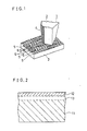
- Fig. 1 is a perspective view showing a pick-up stylus.
- a diamond substrate 2 of a pickup stylus 1 is substantially a prism shaped.
- a cross section of the prism shaped stylus taken parallel to a face of the video disc 3 is of a pentagon-shape, which is made by obliquely cutting a corner of a square, thereby to make a short fifth edge 41.
- On a vertical strip shaped face which is defined by including the short fifth edge 41 form an electrode face to which a metal electrode 4 is applied.
- the video disc 3 is driven in a manner that its part lying immediately under the stylus travels in a direction of a normal line to the electrode face, that is in the direction D.
- the end tip which is the bottom face of the diamond substrate 2 is flatly finished so as to slide with respect to the video disc 3 smoothly.
- the video disc 3 has a conductive surface layer at least on the upper surface thereof, and the conductive layer has a spiral row of a very large number of signal pits 5. Between the row of the signal pits 5, a spiral row of pilot pits 6 is formed.
- capacitance between the electrode 4 and the conductive layer of the video disc changes responding on existence or non-existence of pits under the lower end of the electrode 4.
- an oscillation circuit comprising the capacitance as its resonance circuit, the change of the capacitance can be converted to frequency change of the oscillator output.
- the tracking control of the stylus along the track of the signal pits is attained, for example, by disposing rows of the pilot pits on both sides of the signal pit row in a manner to produce different pilot signal frequencies f, and f 2 , comparing strengths thereof and controlling the tracking so as to obtain equal strengths for both pilot signals of frequencies f, and f 2 .
- the electrode 4 formed on the narrow strip shaped fifth face of pentagonal cross section prism stylus body 1 is bonded in a novel way as is elucidated hereunder.
- FIG. 2 schematically shows cross section along the longitudinal direction of a part of the stylus 1, wherein the conductive layer, for example, vapor deposited metal film 12 is formed with an interface layer 13 on the diamond substrate 11 of the stylus body.
- the interface layer 13 comprises a surface treated layer of the diamond substrate.
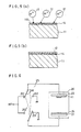
- the surface treated layer preferably comprise roughened diamond surface layer. The inventors found that the roughened layer gives especially strong bonding force when the roughening work is made by a special process to form a very large number of needles on the surface instead of known mechanical grinding of the diamond. Such process is hereinafter elucidated referring to FIG. 3 and subsequent drawings.
- FIG. 3 is a perspective view showing a diamond substrate having a roughened face on a selected face.
- the roughened face is prepared by bombardment of oxygen ion, on the selected diamond substrate. By such bombardment, the selected face is roughened to have a large number of - needle-shaped protrusions 14 as shown by FIG. 3(a).
- a metal layer 12 is deposited with an interface layer 13 consisting of the protrusions 14 of the diamond and sputtered front of the metal filled in the narrow spaces of between the protrusions 14. It is confirmed that by forming such interface layer 13 inbetween, the metal layer 12 is very strongly bonded on the diamond substrate 11.
- the thickness of the protrusion has an optimum range. That is, the preferable range of the size (width or diameter) of the protrusions at its trunk part or at the bottom part is from 0.01 pm to 0.5 ⁇ m.
- the protrusions should be arranged uniformly.
- bonding force of the Ti-film onto the roughened face of the diamond is above 5 kg/mm 2 , which is larger than bonding force by ordinary epoxy adhesive.
- the bonding force sharply decreases, and the surface of the vapor deposited metal electrode becomes rough making the stylus out of utility.
- the thickness or diameter becomes smaller than 0.01 pm, the effect of the roughening of the diamond face is lost, sharply decreasing the bonding force lower than 100 g/mm 2 , allowing the vapor deposited metal film to be easily pealed off from the diamond face by simply applying adhesive tape on the metal film and peal it off, resulting in loss of utility.
- the length of the protrusions' is important for attaining strong bonding force.
- Preferable range of the length is from 0.01 ⁇ m to 0.5 11m which is substantially equal to the thickness or the width of the protrusions.
- the length is above 0.5 ⁇ m the surface of the diamond substrate as well as vapor deposited electrode becomes too rough; and on the contrary when the length is shorter than 0.01 pm, the bonding force becomes to small making the stylus inac- tual.
- metal film to be vapor deposited on the selected face of the diamond substrate may be, other than the above-mentioned Ti, such metal having a suitable mechanical strength and corrosion-resistivity can be used, as Ta, Nb, Hf, Zr, Cr, Mo, Ni or W, and alloys of at least one of them, for example, titanium alloys such as Ti-Ni or Ti-Al-Mo, nitrides of the metals, such as HfN or TiN, carbides of the metal such as TiC, silicide of the metal such as Mo-Si or ferro-alloys such as stainless steels.
- Such conductive material can be formed on the roughened diamond stylus by means of, for example, sputtering.
- Preferable thickness of the conductive film is to be comparable to the length of the protrusions 14.
- the inventors found by the experiments that by selecting the thickness should be within the range from 0.01 ⁇ m to 1 pm, a practical metal electrode having a sheet resistance lower than 10 ⁇ / ⁇ m, and the stylus having such electrode is useful as playback styluses for video disc or audio disc of capacitance type.
- the thickness of the conductive film or coating 12 As a result of the experimental search on the thickness of the conductive film or coating 12, it is found that too large thickness leads to pealing off of the conductive film from the diamond substrate. On the contrary, too thin thickness leads to undesirable increase of the sheet resistance of the conductive layer within the lifetime. It has been found that in order to obtain a long lifetime conductive film, the thickness should be from 0.05 pm to 0.2 pm.
- an over-coating forming of corrosion-prevention layer on the electrode conductive film In order to attain a satisfactory corrosion-resistivity, an over-coating forming of corrosion-prevention layer on the electrode conductive film.
- noble metal such as Pt, Au, Ir or Rh
- stable compound such as SiC
- stable organic compound such as polyethylene, poly- imido or polystylene are preferable.
- Such corrosion-prevention film should be of a thickness within the range of from 0.01 ⁇ m to 0.1 pm, and such film may be formed in a short time by sputtering. By providing such corrosion-prevention film, the electrode can be-stably used without change of characteristics for a long time even in such hard atmosphere of a high relative humidity of over 80%.
- a strong bonding force of over 5 kg/mm 2 is obtainable in accordance with the manufacturing method of the present invention wherein a diamond stylus is made by grinding work of a small lump of diamond bonded on a metal shank to form a diamond substrate, then after roughening a selected face of the substrate by oxygen ion bombardment and sputtering conductive electrode film by sputtering in a cold temperature.
- the direction of the protrusions 14 or needles formed on the substrate face is not necessarily normal to the substrate face as shown by FIG. 3(a) and FIG. 3(b), but may be -oblique as shown by FIG. 4, when the width or diameter and length thereof are within the aforementioned ranges and the protrusions are disposed uniformly on the face. It is confirmed that any angle of tilting of the protrusions 14 may be acceptable, and even the protrusions of such a tilting as having 8° to the substrate face is also effective in increasing the bonding force. Microscopic photograph taken by use of a scanning microscope have proved existence of very fine needle structure which has not hitherto observed.
- FIG. 5(a), FIG. 5(b) and FIG. 6 show a fundamental example of manufacturing.
- the selected face 110 of the diamond stylus 11 is worked by bombardment of ions 17 thereby to form roughened face having needle shaped protrusions 14, as shown in FIG. 5(a).
- the substrate is subject to deposition of the conductive substance by, for example, sputtering, thereby to form the electrode of a conductive film 12 as shown by FIG. 5(b).
- the inventors found that selection of the ion of the bombardment is very important for the increase of the bonding force; and it is found that oxygen ion is most suitable for this purpose.
- oxygen ion bombardment By use of oxygen ion bombardment, the bonding force of the conductive film on the diamond face becomes above 5 kg/mm 2 . The reason is not necessary clear, but by a comparison test with Ar-ion bombardment, which is generally used to clear the substrate surface, the drastic roughening effect is confirmed only for the oxygen-ion bombardment.
- the Ar-ion bombardment does not increase the bonding force of the applied conductive film on the diamond surface as the oxygen-ion bombardment does.
- the oxygen ions not only mechanically bombarding, but also chemically reacting carbon atoms at the surface part of the diamond substrate, and accordingly form considerable recesses on the bombarded surface thereby leaving needle shaped protrusions between the recesses, and thus intensely roughened surface can hold sputter-formed front parts filled in the recesses.
- FIG. 6 is a schematical diagram showing an apparatus for manufacturing the pickup stylus in accordance with the present invention. Some very actual examples of manufacturing the pickup stylus by use of the apparatus of FIG. 6 is elucidated hereafter.
- the sputter etching for roughening the diamond substrate surface is made by the apparatus shown in FIG. 6, by throwing a linked switch SW to the side of the contacts 251 and 251', thereby applying a negative high tension voltage of, for example 1000 V, to a sample holder 22 which holds a diamond substrate 11 in an evacuated chamber 20, with respect to the main electrode 21 which holds a conductive material to be sputtered to form the stylus electrode.
- oxygen gas of, for example 5 x 10- 2 Torr (5 x 1.33 Pa) pressure, is lead in the chamber 20, thereby making glow discharge start between the main electrode 21 and the sample holder 22.
- the depth of the etching may be selected by selecting the etching time.
- the switch SW is changed over to the side'of the contacts 252 and 252', thereby applying the negative high tension voltage to the main electrode 21 and, also at the same time the gas in the chamber 20 is replaced by Ar.
- the material 24 to form the conductive electrode layer 12 held on the main electrode 21 is sputtered and deposited on the face of the diamond substrate 11.
- the thickness of the conductive layer 12 is important for attaining strong bonding force thereof to the diamond substrate 11, and for example, the conductive layer 12 is formed to have a thickness of about 0.1 11m and metalized by known metalizing process.
- the sputter etching process and the subsequent metalizing process may be carried out in sequence without intermission inbetween, and there is no need of heating the substrate to a high temperature, but the processes can be made for the substrate 11 at a room temperature in the chamber 20, and such a satisfactory bonding force of 5 kg/mm 2 or above is obtainable.
- Metalizing the above-mentioned electrode material on the diamond substrate is made by only holding such material on the main electrode 24 in the chamber 20, retaining other parts of the process are the same.
- nitride, carbide or silicide layers are formed as the electrode on the diamond substrate 11, it is possible by holding such metal as Hf, Ti, or Mo on the main electrode 21, and then carrying out a reactive sputtering in the subsequent sputtering by filling the chamber 20 with nitrogen, carbon- containing gas such as metane or acetylene or silicon-containing gas such as silane.
- the diamond substrate provided with the conductive layer formed with a strong bonding force on the former is especially suitable for use far play back pickup stylus in a capacitive type video disc system, since the substrate is resistive to subsequent grinding to make a pickup stylus wherein the conductive layer is ground to such narrow strip as 1 pm width or lower at the end tip part. Shaping of such narrow conductive strip on the diamond stylus by the conventional method has been likely to produce unstability and irregularity of the strip electrode, leading to poor bonding force of the strip electrode on the stylus substrate.
- the metal layer is very strongly bonded and is resistive to mechanical grinding to such narrow width.
- the advantage of the present invention is that the method can be applied even to a very minute construction of the diamond stylus substrate, since the ions having such small sizes of 1 to 10 A are used for the pretreatment (roughening) of the substrate.
- the diamond stylus substrate is cleaned with organic solvent. Then the substrate is put on a water-cooled anode in a high frequency sputtering apparatus. That is, the high frequency etching is made by an inverse sputtering where a negative high tension voltage is applied on the anode.
- the inverse sputtering is made with a high frequency power of 300 W in a mixed atmosphere of argon and oxygen (1:1 in mol ratio) of 3 x 10- 2 Torr (2 x 1.33 Pa) for two minutes. Then after replacing the atmosphere to pure argon gas of 2 x 10- 2 Torr, another inverse sputtering is carried out for 2 minutes.
- needle shaped protrusions are uniformly formed on the selected face of the substrate 11.
- Hf lump put on a target electrode (or main electrode) in the chamber is sputtered in, and using, a pure argon gas of 5 x 10- 3 Torr (5 x 0.13 Pa) at a sputtering power of 45 W for 21 minutes, thereby forming Hf conductive layer on the diamond stylus substrate 11.
- the thickness of the Hf electrode was 0.25 11m and bonding force thereof is over 5 kg/mm 2 .
- one of such metal as Ti, Ta, Nb, Zr, Cr, Ni, Mo or W, such alloy as Ti-Ni or Ti-AI-Mo which contains at least one of above metals, such nitride as HfN or TiN, such carbide as TiC, such silicide, as MoSi or such corrosion-resistive ferro-alloy as stainless steel, is usable.
- Metalizing the above-mentioned electrode material on the diamond substrate is made by only holding such material on the main electrode 24 in the chamber 20, retaining other parts of the process are the same.
- the electrode on the diamond substrate 11 it is possible by holding such metal as Hf, Ti or Mo on the main electrode 21, and then carrying out a reactive sputtering in the subsequent sputtering by filling the chamber 20 with nitrogen, carbon- containing gas such as metane or acetylene or silicon-containing gas such as silane.
- the diamond substrate provided with the conductive layer formed with a strong bonding force on the former is especially suitable for use for play back pickup stylus in a capacitive type video disc system, since the substrate is resistive to subsequent grinding to make a pickup stylus wherein the conductive layer is ground to such narrow-strip as 1 pm width or lower at the end tip part. Shaping of such narrow conductive strip on the diamond stylus by the conventional method has been likely to produce unstability and irregularity of the strip electrode, leading to poor bonding force of the strip electrode on the stylus substrate.
- the metal layer is very strongly bonded and is resistive to mechanical grinding to such narrow width.
- the advantage of the present invention is that the method can be applied even to a very minute construction of the diamond stylus substrate, since the ions having such small sizes of 1 to 10 A are used for the pretreatment (roughening) of the substrate.
- the diamond stylus substrate is-cleaned with organic solvent. Then the substrate is put on a water-cooled anode in a high frequency sputtering apparatus. That is, the high frequency etching is made by an inverse sputtering where a negative high tension voltage is applied on the anode.
- the inverse sputtering is made with a high frequency power of 300 W in a mixed atmosphere of argon and oxygen (1:1 in mol ratio) of 3 x 10- 2 Torr (3 x 1.33 Pa) for two minutes. Then after replacing the atmosphere to pure argon gas of 2 x 10- 2 Torr (2 x 1.33 Pa), another inverse sputtering is carried out for 2 minutes.
- Hf lump put on a target electrode (or main electrode) in the chamber is sputtered by a reactive sputtering in a mixed gas consisting of argon and nitrogen (in the mol ratio of 1:1) of 5 x 10- 3 Torr at a sputtering power of 250 W for 5 minutes, thereby forming HfN conductive layer on the diamond stylus substrate 11.
- the thickness of the HfN electrode was 0.2 ⁇ m and bonding force thereof is over 5 kg/mm 2 .
Landscapes
- Chemical & Material Sciences (AREA)
- Engineering & Computer Science (AREA)
- Ceramic Engineering (AREA)
- Materials Engineering (AREA)
- Structural Engineering (AREA)
- Organic Chemistry (AREA)
- Inorganic Chemistry (AREA)
- Health & Medical Sciences (AREA)
- Toxicology (AREA)
- Crystals, And After-Treatments Of Crystals (AREA)
Claims (5)
Applications Claiming Priority (4)
| Application Number | Priority Date | Filing Date | Title |
|---|---|---|---|
| JP162411/80 | 1980-11-17 | ||
| JP162412/80 | 1980-11-17 | ||
| JP55162412A JPS5786146A (en) | 1980-11-17 | 1980-11-17 | Diamond parts |
| JP16241180A JPS6058200B2 (ja) | 1980-11-17 | 1980-11-17 | ダイヤモンド部品の製造方法 |
Publications (3)
| Publication Number | Publication Date |
|---|---|
| EP0052373A2 EP0052373A2 (de) | 1982-05-26 |
| EP0052373A3 EP0052373A3 (en) | 1983-01-05 |
| EP0052373B1 true EP0052373B1 (de) | 1986-03-12 |
Family
ID=26488216
Family Applications (1)
| Application Number | Title | Priority Date | Filing Date |
|---|---|---|---|
| EP81109722A Expired EP0052373B1 (de) | 1980-11-17 | 1981-11-16 | Verfahren zur Herstellung einer Abtastnadel |
Country Status (3)
| Country | Link |
|---|---|
| US (1) | US4458346A (de) |
| EP (1) | EP0052373B1 (de) |
| DE (1) | DE3174085D1 (de) |
Families Citing this family (7)
| Publication number | Priority date | Publication date | Assignee | Title |
|---|---|---|---|---|
| FR2625190A1 (fr) * | 1987-12-23 | 1989-06-30 | Trt Telecom Radio Electr | Procede de metallisation d'un substrat en silice, quartz, verre, ou en saphir et substrat obtenu par ce procede |
| US5334306A (en) * | 1991-12-11 | 1994-08-02 | At&T Bell Laboratories | Metallized paths on diamond surfaces |
| US5407506A (en) * | 1992-06-04 | 1995-04-18 | Alliedsignal Inc. | Reaction bonding through activation by ion bombardment |
| US5427638A (en) * | 1992-06-04 | 1995-06-27 | Alliedsignal Inc. | Low temperature reaction bonding |
| EP3758853A4 (de) * | 2018-03-01 | 2022-03-02 | DH Technologies Development Pte. Ltd. | Integrierter elektrospray-emitter und verfahren zu seiner herstellung |
| CN113584446A (zh) * | 2021-07-23 | 2021-11-02 | 中国科学院半导体研究所 | 利用磁控溅射在硅衬底上制备的金属铪薄膜、方法和应用 |
| CN116926494B (zh) * | 2023-08-07 | 2024-11-08 | 深圳市博源碳晶科技有限公司 | 一种金刚石铜基复合材料及其制备方法 |
Citations (2)
| Publication number | Priority date | Publication date | Assignee | Title |
|---|---|---|---|---|
| EP0013363A1 (de) * | 1978-12-21 | 1980-07-23 | International Business Machines Corporation | Verfahren zur Herstellung von Lese/Schreibköpfen und nach diesem Verfahren hergestellte Köpfe |
| EP0017360A2 (de) * | 1979-03-19 | 1980-10-15 | Xerox Corporation | Verfahren und Vorrichtung zur Vorbehandlung eines Substrates, Verfahren und Vorrichtung zur Vorbehandlung und Beschichtung eines Substrates mit einem dünnen Metallfilm |
Family Cites Families (10)
| Publication number | Priority date | Publication date | Assignee | Title |
|---|---|---|---|---|
| US3826877A (en) * | 1972-09-06 | 1974-07-30 | Rca Corp | Information playback system stylus |
| US3843846A (en) * | 1973-02-08 | 1974-10-22 | Rca Corp | Demountable capacitive protective coupling for pickup transducers |
| JPS511398A (de) * | 1974-04-04 | 1976-01-08 | Matsushita Electric Industrial Co Ltd | |
| US3945902A (en) * | 1974-07-22 | 1976-03-23 | Rca Corporation | Metallized device and method of fabrication |
| US4013830A (en) * | 1975-05-19 | 1977-03-22 | Rca Corporation | Video disc stylus |
| GB1592361A (en) * | 1976-09-13 | 1981-07-08 | Rca Corp | Stylus manufacture |
| JPS5936336B2 (ja) * | 1977-01-21 | 1984-09-03 | 日本ビクター株式会社 | 走査針 |
| US4104832A (en) * | 1977-03-25 | 1978-08-08 | Rca Corporation | Method for forming keel-tipped stylus for video disc systems |
| GB2069741B (en) * | 1980-02-13 | 1983-08-10 | Victor Company Of Japan | Reproducing stylus for information signal recording mediums of electrostatic capacitance type |
| JPS56117343A (en) * | 1980-02-19 | 1981-09-14 | Victor Co Of Japan Ltd | Reproducing stylus of reproducing element detecting variation in electrostatic capacity value |
-
1981
- 1981-11-09 US US06/319,279 patent/US4458346A/en not_active Expired - Fee Related
- 1981-11-16 DE DE8181109722T patent/DE3174085D1/de not_active Expired
- 1981-11-16 EP EP81109722A patent/EP0052373B1/de not_active Expired
Patent Citations (2)
| Publication number | Priority date | Publication date | Assignee | Title |
|---|---|---|---|---|
| EP0013363A1 (de) * | 1978-12-21 | 1980-07-23 | International Business Machines Corporation | Verfahren zur Herstellung von Lese/Schreibköpfen und nach diesem Verfahren hergestellte Köpfe |
| EP0017360A2 (de) * | 1979-03-19 | 1980-10-15 | Xerox Corporation | Verfahren und Vorrichtung zur Vorbehandlung eines Substrates, Verfahren und Vorrichtung zur Vorbehandlung und Beschichtung eines Substrates mit einem dünnen Metallfilm |
Non-Patent Citations (1)
| Title |
|---|
| Leon I. Massel Handbook of Thin Film Technology, New York, 1970, pages 3-29 and 3-30 * |
Also Published As
| Publication number | Publication date |
|---|---|
| DE3174085D1 (en) | 1986-04-17 |
| EP0052373A3 (en) | 1983-01-05 |
| US4458346A (en) | 1984-07-03 |
| EP0052373A2 (de) | 1982-05-26 |
Similar Documents
| Publication | Publication Date | Title |
|---|---|---|
| US5901021A (en) | Thin-film magnetic head | |
| US6338777B1 (en) | Method and apparatus for sputtering thin films | |
| US4554217A (en) | Process for creating wear and corrosion resistant film for magnetic recording media | |
| Gupta et al. | Mechanical and tribological properties of hard carbon coatings for magnetic recording heads | |
| CN101236747A (zh) | 包括氮氧化铝衬层和类金刚石覆层的磁记录头和介质 | |
| JP2000119843A (ja) | ダイヤモンドライクカーボン硬質多層膜成形体 | |
| EP0474369A1 (de) | Diamantartige Kohlenstoffbeschichtungen | |
| EP0052373B1 (de) | Verfahren zur Herstellung einer Abtastnadel | |
| JPS63311626A (ja) | 磁気記録ディスクの製造方法 | |
| US4056457A (en) | Method of depositing low stress hafnium thin films | |
| JPS62120629A (ja) | 磁気ディスク及びその製造方法 | |
| US4013830A (en) | Video disc stylus | |
| US4060471A (en) | Composite sputtering method | |
| EP0581303A2 (de) | Magnetkopf mit Chromiumnitride-Schutzfilm zum Gebrauch in einem magnetischen Aufzeichnungs- oder Wiedergabegerät und Herstellungsverfahren | |
| JPS60221565A (ja) | ダイヤモンド部品およびその製造方法 | |
| JPH07109561A (ja) | 窒化クロム膜被覆基体 | |
| JPS60212847A (ja) | ダイヤモンド部品 | |
| JPS61210521A (ja) | 磁気デイスクの製造方法 | |
| JP2518424B2 (ja) | 磁気ヘッドおよびその製造方法 | |
| JPS6058200B2 (ja) | ダイヤモンド部品の製造方法 | |
| JP2001297410A (ja) | 薄膜磁気ヘッドおよびその製造方法 | |
| JPH04255909A (ja) | 磁気ディスク用基板およびそれを用いた磁気記録媒体 | |
| JPH07118829A (ja) | 窒化クロム膜被覆基体及びその製造方法 | |
| JPS61215294A (ja) | ダイヤモンド部品の製造方法 | |
| JP2910954B2 (ja) | 磁気ヘッドの製造方法 |
Legal Events
| Date | Code | Title | Description |
|---|---|---|---|
| PUAI | Public reference made under article 153(3) epc to a published international application that has entered the european phase |
Free format text: ORIGINAL CODE: 0009012 |
|
| AK | Designated contracting states |
Designated state(s): DE FR GB |
|
| PUAL | Search report despatched |
Free format text: ORIGINAL CODE: 0009013 |
|
| AK | Designated contracting states |
Designated state(s): DE FR GB |
|
| 17P | Request for examination filed |
Effective date: 19830606 |
|
| GRAA | (expected) grant |
Free format text: ORIGINAL CODE: 0009210 |
|
| AK | Designated contracting states |
Kind code of ref document: B1 Designated state(s): DE FR GB |
|
| REF | Corresponds to: |
Ref document number: 3174085 Country of ref document: DE Date of ref document: 19860417 |
|
| ET | Fr: translation filed | ||
| PLBE | No opposition filed within time limit |
Free format text: ORIGINAL CODE: 0009261 |
|
| STAA | Information on the status of an ep patent application or granted ep patent |
Free format text: STATUS: NO OPPOSITION FILED WITHIN TIME LIMIT |
|
| 26N | No opposition filed | ||
| PGFP | Annual fee paid to national office [announced via postgrant information from national office to epo] |
Ref country code: GB Payment date: 19931108 Year of fee payment: 13 |
|
| PGFP | Annual fee paid to national office [announced via postgrant information from national office to epo] |
Ref country code: FR Payment date: 19931110 Year of fee payment: 13 Ref country code: DE Payment date: 19931110 Year of fee payment: 13 |
|
| PG25 | Lapsed in a contracting state [announced via postgrant information from national office to epo] |
Ref country code: GB Effective date: 19941116 |
|
| GBPC | Gb: european patent ceased through non-payment of renewal fee |
Effective date: 19941116 |
|
| PG25 | Lapsed in a contracting state [announced via postgrant information from national office to epo] |
Ref country code: FR Effective date: 19950731 |
|
| PG25 | Lapsed in a contracting state [announced via postgrant information from national office to epo] |
Ref country code: DE Effective date: 19950801 |
|
| REG | Reference to a national code |
Ref country code: FR Ref legal event code: ST |