EP0052373A2 - Verfahren zur Herstellung einer Abtastnadel - Google Patents
Verfahren zur Herstellung einer Abtastnadel Download PDFInfo
- Publication number
- EP0052373A2 EP0052373A2 EP81109722A EP81109722A EP0052373A2 EP 0052373 A2 EP0052373 A2 EP 0052373A2 EP 81109722 A EP81109722 A EP 81109722A EP 81109722 A EP81109722 A EP 81109722A EP 0052373 A2 EP0052373 A2 EP 0052373A2
- Authority
- EP
- European Patent Office
- Prior art keywords
- accordance
- pickup stylus
- conductive layer
- stylus
- corrosion
- Prior art date
- Legal status (The legal status is an assumption and is not a legal conclusion. Google has not performed a legal analysis and makes no representation as to the accuracy of the status listed.)
- Granted
Links
Images

Classifications
-
- C—CHEMISTRY; METALLURGY
- C04—CEMENTS; CONCRETE; ARTIFICIAL STONE; CERAMICS; REFRACTORIES
- C04B—LIME, MAGNESIA; SLAG; CEMENTS; COMPOSITIONS THEREOF, e.g. MORTARS, CONCRETE OR LIKE BUILDING MATERIALS; ARTIFICIAL STONE; CERAMICS; REFRACTORIES; TREATMENT OF NATURAL STONE
- C04B41/00—After-treatment of mortars, concrete, artificial stone or ceramics; Treatment of natural stone
- C04B41/009—After-treatment of mortars, concrete, artificial stone or ceramics; Treatment of natural stone characterised by the material treated
-
- C—CHEMISTRY; METALLURGY
- C04—CEMENTS; CONCRETE; ARTIFICIAL STONE; CERAMICS; REFRACTORIES
- C04B—LIME, MAGNESIA; SLAG; CEMENTS; COMPOSITIONS THEREOF, e.g. MORTARS, CONCRETE OR LIKE BUILDING MATERIALS; ARTIFICIAL STONE; CERAMICS; REFRACTORIES; TREATMENT OF NATURAL STONE
- C04B41/00—After-treatment of mortars, concrete, artificial stone or ceramics; Treatment of natural stone
- C04B41/0027—Ion-implantation, ion-irradiation or ion-injection
-
- C—CHEMISTRY; METALLURGY
- C04—CEMENTS; CONCRETE; ARTIFICIAL STONE; CERAMICS; REFRACTORIES
- C04B—LIME, MAGNESIA; SLAG; CEMENTS; COMPOSITIONS THEREOF, e.g. MORTARS, CONCRETE OR LIKE BUILDING MATERIALS; ARTIFICIAL STONE; CERAMICS; REFRACTORIES; TREATMENT OF NATURAL STONE
- C04B41/00—After-treatment of mortars, concrete, artificial stone or ceramics; Treatment of natural stone
- C04B41/45—Coating or impregnating, e.g. injection in masonry, partial coating of green or fired ceramics, organic coating compositions for adhering together two concrete elements
- C04B41/50—Coating or impregnating, e.g. injection in masonry, partial coating of green or fired ceramics, organic coating compositions for adhering together two concrete elements with inorganic materials
- C04B41/51—Metallising, e.g. infiltration of sintered ceramic preforms with molten metal
-
- C—CHEMISTRY; METALLURGY
- C04—CEMENTS; CONCRETE; ARTIFICIAL STONE; CERAMICS; REFRACTORIES
- C04B—LIME, MAGNESIA; SLAG; CEMENTS; COMPOSITIONS THEREOF, e.g. MORTARS, CONCRETE OR LIKE BUILDING MATERIALS; ARTIFICIAL STONE; CERAMICS; REFRACTORIES; TREATMENT OF NATURAL STONE
- C04B41/00—After-treatment of mortars, concrete, artificial stone or ceramics; Treatment of natural stone
- C04B41/80—After-treatment of mortars, concrete, artificial stone or ceramics; Treatment of natural stone of only ceramics
- C04B41/81—Coating or impregnation
- C04B41/85—Coating or impregnation with inorganic materials
- C04B41/88—Metals
-
- G—PHYSICS
- G11—INFORMATION STORAGE
- G11B—INFORMATION STORAGE BASED ON RELATIVE MOVEMENT BETWEEN RECORD CARRIER AND TRANSDUCER
- G11B9/00—Recording or reproducing using a method not covered by one of the main groups G11B3/00 - G11B7/00; Record carriers therefor
- G11B9/06—Recording or reproducing using a method not covered by one of the main groups G11B3/00 - G11B7/00; Record carriers therefor using record carriers having variable electrical capacitance; Record carriers therefor
- G11B9/07—Heads for reproducing capacitive information
- G11B9/075—Heads for reproducing capacitive information using mechanical contact with record carrier, e.g. by stylus
-
- Y—GENERAL TAGGING OF NEW TECHNOLOGICAL DEVELOPMENTS; GENERAL TAGGING OF CROSS-SECTIONAL TECHNOLOGIES SPANNING OVER SEVERAL SECTIONS OF THE IPC; TECHNICAL SUBJECTS COVERED BY FORMER USPC CROSS-REFERENCE ART COLLECTIONS [XRACs] AND DIGESTS
- Y10—TECHNICAL SUBJECTS COVERED BY FORMER USPC
- Y10T—TECHNICAL SUBJECTS COVERED BY FORMER US CLASSIFICATION
- Y10T428/00—Stock material or miscellaneous articles
- Y10T428/24—Structurally defined web or sheet [e.g., overall dimension, etc.]
- Y10T428/24802—Discontinuous or differential coating, impregnation or bond [e.g., artwork, printing, retouched photograph, etc.]
- Y10T428/24917—Discontinuous or differential coating, impregnation or bond [e.g., artwork, printing, retouched photograph, etc.] including metal layer
Definitions
- a pickup stylus in accordance with the present invention comprises a diamond substrate of stylus body and a conductive coating formed on a selected face of the diamond substrate, characterized in that
- a first type is a system using a conductive disc having a spiral guide groove for guiding a pickup stylus thereon
- a second type is a system using a conductive disc which does not possess any guide groove but a pickup stylus is servo- controlled to trace a spiral track.
- the present invention is applicable to both of the above-mentioned first and second systems.
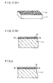
- FIG. 2 schematically shows cross section along the longitudinal direction of a part of'the stylus 1, wherein the conductive layer, for example, vapor deposited metal film 12 is formed with an interface layer 13 on the diamond substrate 11 of the stylus body.
- the interface layer 13 comprises a surface treated layer of the diamond substrate.
- the surface treated layer preferably comprise roughened diamond surface layer. The inventors found that the roughened layer gives especially strong bonding force when the roughening work is made by a special process to form a very large number of needles on the surface instead of known mechanical grinding of the diamond. Such process is hereafter elucidated referring to FIG. 3 and subsequent drawings.
- a metal layer 12 is deposited with an interface layer 13 consisting of the protrusions 14 of the diamond and sputtered front of the metal filled in the narrow spaces of between the protrusions 14. It is confirmed that by forming such interface layer 13 inbetween, the metal layer 12 is very strongly bonded on the diamond substrate 11.
- a strong bonding force of over 5 kg/mm 2 is obtainable in accordance with the manufacturing method of the present invention wherein a diamond stylus is made by grinding work of a small lump of diamond bonded on a metal shank to form a diamond substrate, then after roughening a selected face of the substrate by oxygen ion bombardment and sputtering conductive electrode film by sputtering in a cold temperature.
- the inventors found that selection of the ion of the bombardment is very important for the increase of the bonding force; and it is found that oxygen ion is most suitable for this purpose.
- oxygen ion bombardment By use of oxygen ion bombardment, the bonding force of the conductive film on the diamond face becomes above 5 kg/mm2. The reason is not necessary clear, but by a comparison test with Ar-ion bombardment, which is generally used to clear the substrate surface, the drastic roghening effect is confirmed only for the oxygen-ion bombardment.
- the Ar-ion bombardment does not increase the bonding force of the applied conductive film on the diamond surface as the oxygen-ion bombardment does.
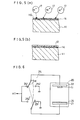
- Hf lump put on a target electrode (or main electrode) in the chamber is sputtered in, and using, a pure argon gas of 5 x 10 -3 Torr at a sputtering power of 45 W for 21 minutes, thereby forming H f conductive layer on the diamond stylus substrate 11.
- the thickness of the Hf electrode was 0.25 ⁇ m and bonding force thereof is over 5 kg/mm 2 .
Landscapes
- Chemical & Material Sciences (AREA)
- Engineering & Computer Science (AREA)
- Ceramic Engineering (AREA)
- Materials Engineering (AREA)
- Structural Engineering (AREA)
- Organic Chemistry (AREA)
- Inorganic Chemistry (AREA)
- Health & Medical Sciences (AREA)
- Toxicology (AREA)
- Crystals, And After-Treatments Of Crystals (AREA)
Applications Claiming Priority (4)
| Application Number | Priority Date | Filing Date | Title |
|---|---|---|---|
| JP16241180A JPS6058200B2 (ja) | 1980-11-17 | 1980-11-17 | ダイヤモンド部品の製造方法 |
| JP55162412A JPS5786146A (en) | 1980-11-17 | 1980-11-17 | Diamond parts |
| JP162412/80 | 1980-11-17 | ||
| JP162411/80 | 1980-11-17 |
Publications (3)
| Publication Number | Publication Date |
|---|---|
| EP0052373A2 true EP0052373A2 (de) | 1982-05-26 |
| EP0052373A3 EP0052373A3 (en) | 1983-01-05 |
| EP0052373B1 EP0052373B1 (de) | 1986-03-12 |
Family
ID=26488216
Family Applications (1)
| Application Number | Title | Priority Date | Filing Date |
|---|---|---|---|
| EP81109722A Expired EP0052373B1 (de) | 1980-11-17 | 1981-11-16 | Verfahren zur Herstellung einer Abtastnadel |
Country Status (3)
| Country | Link |
|---|---|
| US (1) | US4458346A (de) |
| EP (1) | EP0052373B1 (de) |
| DE (1) | DE3174085D1 (de) |
Families Citing this family (7)
| Publication number | Priority date | Publication date | Assignee | Title |
|---|---|---|---|---|
| FR2625190A1 (fr) * | 1987-12-23 | 1989-06-30 | Trt Telecom Radio Electr | Procede de metallisation d'un substrat en silice, quartz, verre, ou en saphir et substrat obtenu par ce procede |
| US5334306A (en) * | 1991-12-11 | 1994-08-02 | At&T Bell Laboratories | Metallized paths on diamond surfaces |
| US5427638A (en) * | 1992-06-04 | 1995-06-27 | Alliedsignal Inc. | Low temperature reaction bonding |
| US5407506A (en) * | 1992-06-04 | 1995-04-18 | Alliedsignal Inc. | Reaction bonding through activation by ion bombardment |
| EP3758853A4 (de) * | 2018-03-01 | 2022-03-02 | DH Technologies Development Pte. Ltd. | Integrierter elektrospray-emitter und verfahren zu seiner herstellung |
| CN113584446A (zh) * | 2021-07-23 | 2021-11-02 | 中国科学院半导体研究所 | 利用磁控溅射在硅衬底上制备的金属铪薄膜、方法和应用 |
| CN116926494B (zh) * | 2023-08-07 | 2024-11-08 | 深圳市博源碳晶科技有限公司 | 一种金刚石铜基复合材料及其制备方法 |
Family Cites Families (12)
| Publication number | Priority date | Publication date | Assignee | Title |
|---|---|---|---|---|
| US3826877A (en) * | 1972-09-06 | 1974-07-30 | Rca Corp | Information playback system stylus |
| US3843846A (en) * | 1973-02-08 | 1974-10-22 | Rca Corp | Demountable capacitive protective coupling for pickup transducers |
| JPS511398A (de) * | 1974-04-04 | 1976-01-08 | Matsushita Electric Industrial Co Ltd | |
| US3945902A (en) * | 1974-07-22 | 1976-03-23 | Rca Corporation | Metallized device and method of fabrication |
| US4013830A (en) * | 1975-05-19 | 1977-03-22 | Rca Corporation | Video disc stylus |
| GB1592361A (en) * | 1976-09-13 | 1981-07-08 | Rca Corp | Stylus manufacture |
| JPS5936336B2 (ja) * | 1977-01-21 | 1984-09-03 | 日本ビクター株式会社 | 走査針 |
| US4104832A (en) * | 1977-03-25 | 1978-08-08 | Rca Corporation | Method for forming keel-tipped stylus for video disc systems |
| US4219853A (en) * | 1978-12-21 | 1980-08-26 | International Business Machines Corporation | Read/write thin film head |
| DE3069815D1 (en) * | 1979-03-19 | 1985-01-31 | Xerox Corp | Method and apparatus for pretreating a substrate, method and apparatus for pretreating a substrate and depositing a thin metallic film thereon |
| NL8000898A (nl) * | 1980-02-13 | 1981-09-16 | Victor Company Of Japan | Weergeefstift voor informatiesignaalregistreermedium van elektrostatisch capacitieve soort. |
| JPS56117343A (en) * | 1980-02-19 | 1981-09-14 | Victor Co Of Japan Ltd | Reproducing stylus of reproducing element detecting variation in electrostatic capacity value |
-
1981
- 1981-11-09 US US06/319,279 patent/US4458346A/en not_active Expired - Fee Related
- 1981-11-16 EP EP81109722A patent/EP0052373B1/de not_active Expired
- 1981-11-16 DE DE8181109722T patent/DE3174085D1/de not_active Expired
Also Published As
| Publication number | Publication date |
|---|---|
| US4458346A (en) | 1984-07-03 |
| EP0052373A3 (en) | 1983-01-05 |
| EP0052373B1 (de) | 1986-03-12 |
| DE3174085D1 (en) | 1986-04-17 |
Similar Documents
| Publication | Publication Date | Title |
|---|---|---|
| US5901021A (en) | Thin-film magnetic head | |
| US4277540A (en) | Thin film magnetic recording medium | |
| US4554217A (en) | Process for creating wear and corrosion resistant film for magnetic recording media | |
| CN101236747A (zh) | 包括氮氧化铝衬层和类金刚石覆层的磁记录头和介质 | |
| US4458346A (en) | Pickup stylus | |
| US4056457A (en) | Method of depositing low stress hafnium thin films | |
| US4013830A (en) | Video disc stylus | |
| US4060471A (en) | Composite sputtering method | |
| US5636092A (en) | Magnetic head having chromium nitride protective film for use in magnetic recording and/or reproducing apparatus and method of manufacturing the same | |
| US5989673A (en) | Caromium-tantalum oxides (Cr-TaOx), sputtering targets and thin film seedlayer/sublayers for thin film magnetic recording media | |
| EP0581303A2 (de) | Magnetkopf mit Chromiumnitride-Schutzfilm zum Gebrauch in einem magnetischen Aufzeichnungs- oder Wiedergabegerät und Herstellungsverfahren | |
| JP2000087218A (ja) | 高密着性炭素皮膜形成材及びその製法 | |
| US20110223332A1 (en) | Method for depositing cubic boron nitride thin film | |
| JPS60221565A (ja) | ダイヤモンド部品およびその製造方法 | |
| JPH07109561A (ja) | 窒化クロム膜被覆基体 | |
| US20040206117A1 (en) | Mold for press-molding glass optical articles and method for making the mold | |
| JPS60212847A (ja) | ダイヤモンド部品 | |
| JPH04255909A (ja) | 磁気ディスク用基板およびそれを用いた磁気記録媒体 | |
| JP2518424B2 (ja) | 磁気ヘッドおよびその製造方法 | |
| JPH07118829A (ja) | 窒化クロム膜被覆基体及びその製造方法 | |
| JPS6058200B2 (ja) | ダイヤモンド部品の製造方法 | |
| US4243395A (en) | Method for precision grinding of hard, pointed materials | |
| JP3117378B2 (ja) | 摺動部材 | |
| JP3428720B2 (ja) | 光学素子成形用型 | |
| JP2910953B2 (ja) | 磁気ヘッドの製造方法 |
Legal Events
| Date | Code | Title | Description |
|---|---|---|---|
| PUAI | Public reference made under article 153(3) epc to a published international application that has entered the european phase |
Free format text: ORIGINAL CODE: 0009012 |
|
| AK | Designated contracting states |
Designated state(s): DE FR GB |
|
| PUAL | Search report despatched |
Free format text: ORIGINAL CODE: 0009013 |
|
| AK | Designated contracting states |
Designated state(s): DE FR GB |
|
| 17P | Request for examination filed |
Effective date: 19830606 |
|
| GRAA | (expected) grant |
Free format text: ORIGINAL CODE: 0009210 |
|
| AK | Designated contracting states |
Kind code of ref document: B1 Designated state(s): DE FR GB |
|
| REF | Corresponds to: |
Ref document number: 3174085 Country of ref document: DE Date of ref document: 19860417 |
|
| ET | Fr: translation filed | ||
| PLBE | No opposition filed within time limit |
Free format text: ORIGINAL CODE: 0009261 |
|
| STAA | Information on the status of an ep patent application or granted ep patent |
Free format text: STATUS: NO OPPOSITION FILED WITHIN TIME LIMIT |
|
| 26N | No opposition filed | ||
| PGFP | Annual fee paid to national office [announced via postgrant information from national office to epo] |
Ref country code: GB Payment date: 19931108 Year of fee payment: 13 |
|
| PGFP | Annual fee paid to national office [announced via postgrant information from national office to epo] |
Ref country code: FR Payment date: 19931110 Year of fee payment: 13 Ref country code: DE Payment date: 19931110 Year of fee payment: 13 |
|
| PG25 | Lapsed in a contracting state [announced via postgrant information from national office to epo] |
Ref country code: GB Effective date: 19941116 |
|
| GBPC | Gb: european patent ceased through non-payment of renewal fee |
Effective date: 19941116 |
|
| PG25 | Lapsed in a contracting state [announced via postgrant information from national office to epo] |
Ref country code: FR Effective date: 19950731 |
|
| PG25 | Lapsed in a contracting state [announced via postgrant information from national office to epo] |
Ref country code: DE Effective date: 19950801 |
|
| REG | Reference to a national code |
Ref country code: FR Ref legal event code: ST |