EP0052373A2 - Method of manufacturing a pickup stylus - Google Patents
Method of manufacturing a pickup stylus Download PDFInfo
- Publication number
- EP0052373A2 EP0052373A2 EP81109722A EP81109722A EP0052373A2 EP 0052373 A2 EP0052373 A2 EP 0052373A2 EP 81109722 A EP81109722 A EP 81109722A EP 81109722 A EP81109722 A EP 81109722A EP 0052373 A2 EP0052373 A2 EP 0052373A2
- Authority
- EP
- European Patent Office
- Prior art keywords
- accordance
- pickup stylus
- conductive layer
- stylus
- corrosion
- Prior art date
- Legal status (The legal status is an assumption and is not a legal conclusion. Google has not performed a legal analysis and makes no representation as to the accuracy of the status listed.)
- Granted
Links
Images

Classifications
-
- C—CHEMISTRY; METALLURGY
- C04—CEMENTS; CONCRETE; ARTIFICIAL STONE; CERAMICS; REFRACTORIES
- C04B—LIME, MAGNESIA; SLAG; CEMENTS; COMPOSITIONS THEREOF, e.g. MORTARS, CONCRETE OR LIKE BUILDING MATERIALS; ARTIFICIAL STONE; CERAMICS; REFRACTORIES; TREATMENT OF NATURAL STONE
- C04B41/00—After-treatment of mortars, concrete, artificial stone or ceramics; Treatment of natural stone
- C04B41/009—After-treatment of mortars, concrete, artificial stone or ceramics; Treatment of natural stone characterised by the material treated
-
- C—CHEMISTRY; METALLURGY
- C04—CEMENTS; CONCRETE; ARTIFICIAL STONE; CERAMICS; REFRACTORIES
- C04B—LIME, MAGNESIA; SLAG; CEMENTS; COMPOSITIONS THEREOF, e.g. MORTARS, CONCRETE OR LIKE BUILDING MATERIALS; ARTIFICIAL STONE; CERAMICS; REFRACTORIES; TREATMENT OF NATURAL STONE
- C04B41/00—After-treatment of mortars, concrete, artificial stone or ceramics; Treatment of natural stone
- C04B41/0027—Ion-implantation, ion-irradiation or ion-injection
-
- C—CHEMISTRY; METALLURGY
- C04—CEMENTS; CONCRETE; ARTIFICIAL STONE; CERAMICS; REFRACTORIES
- C04B—LIME, MAGNESIA; SLAG; CEMENTS; COMPOSITIONS THEREOF, e.g. MORTARS, CONCRETE OR LIKE BUILDING MATERIALS; ARTIFICIAL STONE; CERAMICS; REFRACTORIES; TREATMENT OF NATURAL STONE
- C04B41/00—After-treatment of mortars, concrete, artificial stone or ceramics; Treatment of natural stone
- C04B41/45—Coating or impregnating, e.g. injection in masonry, partial coating of green or fired ceramics, organic coating compositions for adhering together two concrete elements
- C04B41/50—Coating or impregnating, e.g. injection in masonry, partial coating of green or fired ceramics, organic coating compositions for adhering together two concrete elements with inorganic materials
- C04B41/51—Metallising, e.g. infiltration of sintered ceramic preforms with molten metal
-
- C—CHEMISTRY; METALLURGY
- C04—CEMENTS; CONCRETE; ARTIFICIAL STONE; CERAMICS; REFRACTORIES
- C04B—LIME, MAGNESIA; SLAG; CEMENTS; COMPOSITIONS THEREOF, e.g. MORTARS, CONCRETE OR LIKE BUILDING MATERIALS; ARTIFICIAL STONE; CERAMICS; REFRACTORIES; TREATMENT OF NATURAL STONE
- C04B41/00—After-treatment of mortars, concrete, artificial stone or ceramics; Treatment of natural stone
- C04B41/80—After-treatment of mortars, concrete, artificial stone or ceramics; Treatment of natural stone of only ceramics
- C04B41/81—Coating or impregnation
- C04B41/85—Coating or impregnation with inorganic materials
- C04B41/88—Metals
-
- G—PHYSICS
- G11—INFORMATION STORAGE
- G11B—INFORMATION STORAGE BASED ON RELATIVE MOVEMENT BETWEEN RECORD CARRIER AND TRANSDUCER
- G11B9/00—Recording or reproducing using a method not covered by one of the main groups G11B3/00 - G11B7/00; Record carriers therefor
- G11B9/06—Recording or reproducing using a method not covered by one of the main groups G11B3/00 - G11B7/00; Record carriers therefor using record carriers having variable electrical capacitance; Record carriers therefor
- G11B9/07—Heads for reproducing capacitive information
- G11B9/075—Heads for reproducing capacitive information using mechanical contact with record carrier, e.g. by stylus
-
- Y—GENERAL TAGGING OF NEW TECHNOLOGICAL DEVELOPMENTS; GENERAL TAGGING OF CROSS-SECTIONAL TECHNOLOGIES SPANNING OVER SEVERAL SECTIONS OF THE IPC; TECHNICAL SUBJECTS COVERED BY FORMER USPC CROSS-REFERENCE ART COLLECTIONS [XRACs] AND DIGESTS
- Y10—TECHNICAL SUBJECTS COVERED BY FORMER USPC
- Y10T—TECHNICAL SUBJECTS COVERED BY FORMER US CLASSIFICATION
- Y10T428/00—Stock material or miscellaneous articles
- Y10T428/24—Structurally defined web or sheet [e.g., overall dimension, etc.]
- Y10T428/24802—Discontinuous or differential coating, impregnation or bond [e.g., artwork, printing, retouched photograph, etc.]
- Y10T428/24917—Discontinuous or differential coating, impregnation or bond [e.g., artwork, printing, retouched photograph, etc.] including metal layer
Definitions
- a pickup stylus in accordance with the present invention comprises a diamond substrate of stylus body and a conductive coating formed on a selected face of the diamond substrate, characterized in that
- a first type is a system using a conductive disc having a spiral guide groove for guiding a pickup stylus thereon
- a second type is a system using a conductive disc which does not possess any guide groove but a pickup stylus is servo- controlled to trace a spiral track.
- the present invention is applicable to both of the above-mentioned first and second systems.
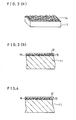
- FIG. 2 schematically shows cross section along the longitudinal direction of a part of'the stylus 1, wherein the conductive layer, for example, vapor deposited metal film 12 is formed with an interface layer 13 on the diamond substrate 11 of the stylus body.
- the interface layer 13 comprises a surface treated layer of the diamond substrate.
- the surface treated layer preferably comprise roughened diamond surface layer. The inventors found that the roughened layer gives especially strong bonding force when the roughening work is made by a special process to form a very large number of needles on the surface instead of known mechanical grinding of the diamond. Such process is hereafter elucidated referring to FIG. 3 and subsequent drawings.
- a metal layer 12 is deposited with an interface layer 13 consisting of the protrusions 14 of the diamond and sputtered front of the metal filled in the narrow spaces of between the protrusions 14. It is confirmed that by forming such interface layer 13 inbetween, the metal layer 12 is very strongly bonded on the diamond substrate 11.
- a strong bonding force of over 5 kg/mm 2 is obtainable in accordance with the manufacturing method of the present invention wherein a diamond stylus is made by grinding work of a small lump of diamond bonded on a metal shank to form a diamond substrate, then after roughening a selected face of the substrate by oxygen ion bombardment and sputtering conductive electrode film by sputtering in a cold temperature.
- the inventors found that selection of the ion of the bombardment is very important for the increase of the bonding force; and it is found that oxygen ion is most suitable for this purpose.
- oxygen ion bombardment By use of oxygen ion bombardment, the bonding force of the conductive film on the diamond face becomes above 5 kg/mm2. The reason is not necessary clear, but by a comparison test with Ar-ion bombardment, which is generally used to clear the substrate surface, the drastic roghening effect is confirmed only for the oxygen-ion bombardment.
- the Ar-ion bombardment does not increase the bonding force of the applied conductive film on the diamond surface as the oxygen-ion bombardment does.
- Hf lump put on a target electrode (or main electrode) in the chamber is sputtered in, and using, a pure argon gas of 5 x 10 -3 Torr at a sputtering power of 45 W for 21 minutes, thereby forming H f conductive layer on the diamond stylus substrate 11.
- the thickness of the Hf electrode was 0.25 ⁇ m and bonding force thereof is over 5 kg/mm 2 .
Landscapes
- Chemical & Material Sciences (AREA)
- Engineering & Computer Science (AREA)
- Ceramic Engineering (AREA)
- Materials Engineering (AREA)
- Structural Engineering (AREA)
- Organic Chemistry (AREA)
- Inorganic Chemistry (AREA)
- Health & Medical Sciences (AREA)
- Toxicology (AREA)
- Crystals, And After-Treatments Of Crystals (AREA)
Abstract
Description
- The present invention relates to an improvement in a pickup stylus, especially for playing back in a capacity type video and/or audio disc player, and making the pickup stylus.
- In the capacity type video and/or audio disc player, as is well known, a recording disc having a conductive part carrying signal thereon is used and a pickup stylus having an electrode thereon traces a fine spiral track on the disc, the track having minute array of pits so that a capacity variation between the electrode on the pickup stylus and the conductive part of the disc is induced to produce electric signal thereby.
- For the stylus body, a diamond stylus is used because of its abrasion-durability, and known pickup stylus has metal electrode which is formed on a mirror finished side face thereof by vapor deposition or the like. However, such conventional pickup stylus has a shortcoming that bonding of the metal electrode on the stylus body is not sufficiently strong, and therefore, the metal electrode is likely to peal off partly from the diamond stylus body during finishing process of the stylus or during use. When such peal off takes place, the manufacturing yield of the stylus falls down, or spoiling play back characteristic or further making the play back impossible.
- The present invention purposes to provide a novel pickup stylus.
- The present invention more particularly purposes to provide a novel pickup stylus for use in playing back video and/or audio signal recorded on a capacity type recording disc.
- The present invention can provide a pickup stylus whereon electrode of a conductive material is strongly bonded.
- The present invention can provide a method of manufacturing the pickup stylus, whereby a stable long life of good performance is obtainable with a high yield of manufacturing.
-
- FIG. 1 is a general perspective view showing a part of a pickup stylus embodying the present invention and a part of a capacity type recording disc as an example of disc, whereon the pickup stylus slides.
- FIG. 2 is a schematic cross-sectional view of the pickup stylus embodying the present invention.
- FIG. 3(a) is a perspective view of a part of the pickup stylus showing a step of manufacturing the pickup stylus embodying the present invention.
- FIG. 3(b) is a cross-sectional view of a part of the pickup stylus of FIG. 3(a).
- FIG. 4 is a cross-sectional view of a part of another pickup stylus embodying the present invention.
- FIG. 5(a) is a cross-sectional view of a part of the pickup stylus showing a step of manufacturing the pickup stylus in accordance with the present invention.
- FIG. 5(b) is a cross-sectional view of a part of the pickup stylus showing a subsequent step of manufacturing the pickup stylus in accordance with the present invention.
- FIG. 6 is a circuit diagram and schematic sectional view of working apparatus for manufacturing pickup stylus embodying the present invention.
- A pickup stylus in accordance with the present invention comprises a diamond substrate of stylus body and a conductive coating formed on a selected face of the diamond substrate,
characterized in that - the conductive coating is formed on the selected face with an interface layer inbetween, the interface layer having a roughened front of the diamond formed on the selected face and the substance of the conductive coating integral to the conductive coating and filled in concave spaces on said roughened front.
- Method of manufacturing a pickup stylus in accordance with the present invention comprises the steps of
- roughening a selected face of a diamond substrate by means of ion-bombardment, thereby forming a roughened face, and
- forming a conductive coating on the roughened face.
- There are two types of capacity type video and/or audio disc player, A first type is a system using a conductive disc having a spiral guide groove for guiding a pickup stylus thereon, and a second type is a system using a conductive disc which does not possess any guide groove but a pickup stylus is servo- controlled to trace a spiral track. The present invention is applicable to both of the above-mentioned first and second systems.
- FIG. 1 is a perspective view showing principal part of an example of the second type system. A
diamond substrate 2 of apickup stylus 1 is substantially a prism shaped. A cross section of the prism shaped stylus taken parallel to a face of thevideo disc 3 is of a pentagon-shape, which is made by obliquely cutting a corner of a square, thereby to make a short fifth edge 41. On a vertical strip shaped face which is defined by including the short fifth edge 41 form an electrode face to which a metal electrode 4 is applied. Thevideo disc 3 is driven in a manner that its part lying immediately under the stylus travels in a direction of a normal line to the electrode face, that is in the direction D. The end tip, which is the bottom face of thediamond substrate 2 is flatly finished so as to slide with respect to thevideo disc 3 smoothly. Thevideo disc 3 has a conductive surface layer at least on the upper surface thereof, and the conductive layer has a spiral row of a very large number ofsignal pits 5. Between the row of thesignal pits 5, a spiral row ofpilot pits 6 is formed. When the video disc is rotated, capacitance between the electrode 4 and the conductive layer of the video disc changes responding on existence or non-existence of pits under the lower end of the electrode 4. By constituting an oscillation circuit comprising the capacitance as its resonance circuit, the change of the capacitance can be converted to frequency change of the oscillator output. The tracking control of the stylus along the track of the signal pits : is attained, for example, by disposing rows of the pilot pits on both sides of the signal pit row in a manner to produce different pilot signal frequencies f1 and f2, comparing strengths thereof and controlling the tracking so as to obtain equal strengths for both pilot signals of frequencies f1 and f2. - The electrode 4 formed on the narrow strip shaped fifth face of pentagonal cross section
prism stylus body 1 is bonded in a novel way as is elucidated hereunder. - FIG. 2 schematically shows cross section along the longitudinal direction of a part of'the
stylus 1, wherein the conductive layer, for example, vapor depositedmetal film 12 is formed with aninterface layer 13 on thediamond substrate 11 of the stylus body. Theinterface layer 13 comprises a surface treated layer of the diamond substrate. Experiments revealed that the surface treated layer preferably comprise roughened diamond surface layer. The inventors found that the roughened layer gives especially strong bonding force when the roughening work is made by a special process to form a very large number of needles on the surface instead of known mechanical grinding of the diamond. Such process is hereafter elucidated referring to FIG. 3 and subsequent drawings. - FIG. 3 is a perspective view showing a diamond substrate having a roughened face on a selected face. The roughened face is prepared by bombardment of ion, preferably oxygen ion, on the selected diamond substrate. By such bombardment, the selected face is roughned to have a large number of needle-
shaped protrusions 14 as shown by FIG. 3(a). - Then, by means of sputtering a metal, for example Ti, on the roughened face having the
protrusions 14, ametal layer 12 is deposited with aninterface layer 13 consisting of theprotrusions 14 of the diamond and sputtered front of the metal filled in the narrow spaces of between theprotrusions 14. It is confirmed that by formingsuch interface layer 13 inbetween, themetal layer 12 is very strongly bonded on thediamond substrate 11. - Through experimental research, the inventors found that the thickness of the protrusion has an optimum range. That is, the preferable range of the size (width or diameter) of the protrusion at its trunk part or at the bottom part is from 0.01 µm to 0.5 µm.
- The protrusion should be arranged uniformly. When the size is within this range, for vapor deposited metal film of Ti of 0.2 µm thick, bonding force of the Ti-film onto the roughened face of the diamond is above 5 kg/mm2, which is larger than bonding force by ordinary epoxy adhesive. As the thickness or diameter becomes larger than 0.5 µm, the bonding force sharply decreases, and the surface of the vapor deposited metal electrode becomes rough making the stylus out of utility. On the contrary, as the thickness or diameter becomes smaller than 0.01 µm, the effect of the roughening of the diamond face is lost, sharply decreasing the bonding force lower than 100 g/mm2, allowing the vapor deposited metal film to be easily pealed off from the diamond face by simply applying adhesive tape on the metal film and peal if off, resulting in loss of utility.
- On the other hand, the length of the protrusions is important for attaining strong bonding force. Preferable range of the length is from 0.01 µm to 0.5 µm which is substantially equal to the thickness or the width of the protrusions. When the length is above 0.5 µm the surface of the diamond substrate as well as vapor deposited electrode becomes too rough; and on the contrary when the length is shorter than 0.01 pm, the bonding force becomes to small making the stylus inactual.
- For metal film to be vapor deposited on the selected face of the diamond substrate may be, other than the above-mentioned Ti, such metal having a suitable-mechanical strength and corrosion-resistivity can be used, as Ta, Nb, Hf, Zr, Cr, Mo, Ni or W, and alloys of at least one of them, for example, titanium alloys such as Ti-Ni or Ti-Al-Mo, nitrides of the metals such as HfN or TiN, carbides of the metal such as TiC, silicide of the metal such as Mo-Si or ferro-alloys such as stainless steels. Such conductive material can be formed on the roughened diamond stylus by means of, for example, sputtering. Preferable thickness of the conductive film is to be comparable to the length of the
protrusions 14. The inventors found by the experiments that by selecting the thickness should'be within the range from 0.01 pm to 1 pm, a practical metal electrode having a sheet resistance lower than 10 Ω/□µm, and the stylus having such electrode is useful as playback styluses for video disc or audio disc of capacitance type. - As a result of the experimental search on the thickness of the conductive film or
coating 12, it is found that too large thickness leads to pealing off of the conductive film from the diamond substrate. On the contrary, too thin thickness leads to undesirable increase of the sheet resistance of the conductive layer within the lifetime. It has been found that in order to obtain a long lifetime conductive film, the thickness should be from 0.05 µm to 0.2 µm. - In order to attain a satisfactory corrosion-resistivity, an over-coating forming of corrosion-prevention layer on the electrode conductive film. For such purpose, noble metal such as Pt, Au, Ir or Rh, stable compound such as SiC, stable organic compound such as polyethylene, polyimido or polystylene are preferable. Such corrosion-prevention film should be of a thickness within the range of from 0.01 µm to 0.1 pm, and such film may be formed in a short time by sputtering. By providing such corrosion-prevention film, the electrode can be stably used without change of characteristics for a long time even in such hard atmosphere of a high relative humidity of over 80%.
- According to the method and construction in accordance with the present invention, no thermal diffusion process is necessary after sputtering of the conductive electrode, in contradistinction from the conventional process where such thermal diffusion as 800°C to 1000°C for 60 minutes has been necessary in order to increase the bonding force. For example, a strong bonding force of over 5 kg/mm 2 is obtainable in accordance with the manufacturing method of the present invention wherein a diamond stylus is made by grinding work of a small lump of diamond bonded on a metal shank to form a diamond substrate, then after roughening a selected face of the substrate by oxygen ion bombardment and sputtering conductive electrode film by sputtering in a cold temperature.
- The direction of the
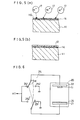
protrusions 14 or needles formed on the substrate face is not necessarily normal to the substrate face as shown by FIG. 3(a) and FIG. 3(b), but may be oblique as shown by FIG. 4, when the width or diameter and length thereof are within the aforementioned ranges and the protrusions are disposed uniformly on the face. It is confirmed that any angle of tilting of theprotrusions 14 may be acceptable, and even the protrusions of such a tilting as having 8° to the substrate face is also effective in increasing the bonding force. Microscopic photograph taken by use of a scanning microscope have proved existence of very fine needle structure which has not hitherto observed. - Process of manufacturing in accordance with the present invention is elucidated more in detail referring to FIG. 5(a), FIG. 5(b) and FIG. 6 which show a fundamental example of manufacturing.
- Firstly, the selected
face 110 of thediamond stylus 11 is worked by bombardment ofions 17 thereby to form roughened face having needle shapedprotrusions 14, as shown by FIG. 5(a). Secondly, the substrate is subject to deposition of the conductive substance by, for example, sputtering, thereby to form the electrode of aconductive film 12 as shown by FIG. 5(b). - Through an intensive experimental research, the inventors found that selection of the ion of the bombardment is very important for the increase of the bonding force; and it is found that oxygen ion is most suitable for this purpose. By use of oxygen ion bombardment, the bonding force of the conductive film on the diamond face becomes above 5 kg/mm2. The reason is not necessary clear, but by a comparison test with Ar-ion bombardment, which is generally used to clear the substrate surface, the drastic roghening effect is confirmed only for the oxygen-ion bombardment. The Ar-ion bombardment does not increase the bonding force of the applied conductive film on the diamond surface as the oxygen-ion bombardment does.
- It may be supposed that the oxygen ions, not only mechanically bombarding, but also chemically reacting carbon atoms at the surface part of the diamond substrate, and accordingly form considerable recesses on the bombarded surface thereby leaving needle shaped protrusions between the recesses, and thus intensely roughened surface can hold sputter-formed front parts filled in the recesses.
- The inventors found that the roughening process including such kind of the ion bombardment can be most effectively carried but by the sputtering. FIG. 6 is a schematical diagram showing an apparatus for manufacturing the pickup stylus in accordance with the present invention. Some very actual examples of manufacturing the pickup stylus by use of the apparatus of FIG. 6 is elucidated hereafter.
- First, the sputter etching for roughening the diamond substrate surface is made by the apparatus shown in FIG. 6, by throwing a linked switch SW to the side of the
contacts 251 and 251', thereby applying a negative high tension voltage of, for example 1000 V, to asample holder 22 which holds adiamond substrate 11 in an evacuatedchamber 20, with respect to themain electrode 21 which holds a conductive material to be sputtered to form the stylus electrode. In this sputter etching process, oxygen gas of, for example 5 x 10 -2 Torr pressure, is lead in thechamber 20, thereby making glow discharge start between themain electrode 21 and thesample holder 22. Oxygen ion produced by the glow discharge bombard the surface of thesubstrate 11 and sputter-etches the surface part of the substrate by a depth of about 0.05 µm. The depth of the etching may be selected by selecting the etching time. After finishing the sputter etching, the switch SW is changed over to the side of thecontacts 252 and 252', thereby applying the negative high tension voltage to themain electrode 21 and, also at the same time the gas in thechamber 20 is replaced by Ar. The material 24 to form theconductive electrode layer 12 held on themain electrode 21 is sputtered and deposited on the face of thediamond substrate 11. As has been elucidated, the thickness of the conductive layer 12- is important for attaining strong bonding force thereof to thediamond substrate 11, and for example, theconductive layer 12 is formed to have a thickness of about 0.1 µm and metalized by known metalizing process. According to the method of the present invention, the sputter etching process and the subsequent metalizing process may be carried out in sequence without intermission inbetween, and there is no need of heating the substrate to a high temperature, but the processes can be made for thesubstrate 11 at a room temperature in thechamber 20, and such a satisfactory bonding force of 5 kg/mm2 or above is obtainable. - For the material to form a conductive electrode, other than the above-mentioned Hf, one of such metal as Ti, Ta, Nb, Zr, Cr, Ni, Mo or W, such alloy as Ti-Ni or Ti-Al-Mo which contains at least one of above metals, such nitride as HfN or TiN, such carbide as TiC, such silicide as MoSi or such corrosion-resistive ferro-alloy as stainless steel, is usable. Metalizing the above-mentioned electrode material on the diamond substrate is made by only holding such material on the
main electrode 24 in thechamber 20, retaining other parts of the process are the same. Alternatively, in case the nitride, carbide or silicide layers are formed as the electrode on thediamond substrate 11, it is possible by holding such metal as Hf, Ti or Mo on themain electrode 21, and then carrying out a reactive sputtering in the subsequent sputtering by filling thechamber 20 with nitrogen, carbon-containing gas such as metane or acetylene or silicon-containing gas such as silane. - The diamond substrate provided with the conductive layer formed with a strong bonding force on the former is especially suitable for use for play back pickup stylus in a capacitive type video disc system, since the substrate is resistive to subsequent grinding to make a pickup stylus wherein the conductive layer is ground to such narrow strip as 1 ym width or lower at the end tip part. Shaping of such narrow conductive strip on the diamond stylus by the conventional method has been likely to produce unstability and irregularity of the strip electrode, leading to poor bonding force of the strip electrode on the stylus substrate. However, in the example of the present invention method, the metal layer is very strongly bonded and is resistive to mechanical grinding to such narrow width.
- The advantage of the present invention is that the method can be applied even to a very minute construction of the diamond stylus substrate, since 0 the ions having such small sizes of 1 to 10 A are used for the pretreatment (roughening) of the substrate.
- Firstly, the diamond stylus substrate is cleaned with organic solvent. Then the substrate is put on a water-cooled anode in a high frequency sputtering apparatus. That is, the high frequency etching is made by an inverse sputtering where a negative high tension voltage is applied on the anode. The inverse sputtering is made with a high frequency power of 300 W in a mixed atmosphere of argon and oxygen (1 : 1 in mol ratio) of 3 x 10⁻² Torr for two minutes. Then after replacing the atmosphere to pure argon gas of 2 x 10⁻² Torr, another inverse sputtering is carried out for 2 minutes. Thus, needle shaped protrusions are uniformly formed on the selected face of the
substrate 11. Subsequently, Hf lump put on a target electrode (or main electrode) in the chamber is sputtered in, and using, a pure argon gas of 5 x 10⁻³ Torr at a sputtering power of 45 W for 21 minutes, thereby forming Hf conductive layer on thediamond stylus substrate 11. The thickness of the Hf electrode was 0.25 µm and bonding force thereof is over 5 kg/mm2. When the substrate is ground to make a play back pickup stylus of a video disc player shown in FIG. 1, wherein the strip shaped conductive electrode 4 is under 1 µm wide, the system shows a satisfactorily stable (constant) C/N ratio (carrier to noise ratio) even after continuous play back of-210 hours. - For the material to form a conductive electrode, other than the above-mentioned Hf, one of such metal as Ti, Ta, Nb, Zr, Cr, Ni, Mo or W, such alloy as Ti-Ni or Ti-Al-Mo which contains at least one of above metals, such nitride as HfN or TiN, such carbide as TiC, such silicide as MoSi or such corrosion-resistive ferro-alloy as stainless steel, is usable. Metalizing the above-mentioned electrode material on the diamond substrate is made by only holding such material on the
main electrode 24 in thechamber 20, retaining other parts of the process are the same. Alternatively, in case the nitride, carbide or silicide layers are formed as the electrode on thediamond substrate 11, it is possible by holding such metal as Hf, Ti or Mo on themain electrode 21, and then carrying out a reactive sputtering in the subsequent sputtering by filling thechamber 20 with nitrogen, carbon-containing gas such as metane or acetylene or silicon-containing gas such as silane. - The diamond substrate provided with the conductive layer formed with a strong bonding force on the former is especially suitable for use for play back pickup'stylus in a capacitive type video disc system, since the substrate is resistive to subsequent grinding to make a pickup stylus wherein the conductive layer is ground to such narrow strip as 1 µm width or lower at the end tip part. Shaping of such narrow conductive strip on the diamond stylus by the conventional method has been likely to produce unstability and irregularity of the strip electrode, leading to poor bonding force of the strip electrode on the stylus substrate. However, in the example of the present invention method, the metal layer is very strongly bonded and is resistive to mechanical grinding to such narrow width.
- The advantage of the present invention is that the method can be applied even to a very minute construction of the diamond stylus substrate, since the ions having such small sizes of 1 to 10 Å are used for the pretreatment (roughning) of the substrate.
- Firstly, the diamond stylus substrate is cleaned with organic solvent. Then the substrate is put on a water-cooled anode in a high frequency sputter- ling apparatus. That is, the high frequency etching is made by an inverse sputtering where a negative high tension voltage is applied on the anode. The inverse sputtering is made with a high frequency power of 300 W in a mixed atmosphere of argon and oxygen (1 : 1 in mol ratio) of 3 x 10⁻² Torr for two minutes. Then after replacing the atmosphere to pure argon gas of 2 x 10⁻² Torr, another inverse sputtering is carried out for 2 minutes. Thus, needle shaped protrusions are uniformly formed on the selected face of the
substrate 11. Subsequently, Hf lump put on a target electrode (or main electrode) in the chamber is sputtered by a reactive sputtering in a mixed gas consisting of argon and nitrogen (in the mol ratio of 1 : 1) of 5 x 10⁻³ Torr at a sputtering power of 250 W for 5 minutes, thereby forming HfN conductive layer on thediamond stylus substrate 11. The thickness of the HfN electrode was 0.2 µm and bonding force thereof is over 5 kg/mm2. When the substrate is ground to make a play back pickup stylus of a video disc player, shown in FIG. 1, wherein the strip shaped conductive electrode 4 is under 1 µm wide, the system shows a satisfactorily stable (constant) C/N ratio (carrier to noise ratio) even after continuous play back of 300 hours.
Claims (39)
characterized in that
said conductive layer is formed on said selected face with an interface layer inbetween, said interface layer having a roughened front of the diamond formed on said selected face and said substance of said conductive layer integral to the conductive coating and filled in concave spaces on said roughened front.
Applications Claiming Priority (4)
| Application Number | Priority Date | Filing Date | Title |
|---|---|---|---|
| JP162411/80 | 1980-11-17 | ||
| JP162412/80 | 1980-11-17 | ||
| JP55162412A JPS5786146A (en) | 1980-11-17 | 1980-11-17 | Diamond parts |
| JP16241180A JPS6058200B2 (en) | 1980-11-17 | 1980-11-17 | How to manufacture diamond parts |
Publications (3)
| Publication Number | Publication Date |
|---|---|
| EP0052373A2 true EP0052373A2 (en) | 1982-05-26 |
| EP0052373A3 EP0052373A3 (en) | 1983-01-05 |
| EP0052373B1 EP0052373B1 (en) | 1986-03-12 |
Family
ID=26488216
Family Applications (1)
| Application Number | Title | Priority Date | Filing Date |
|---|---|---|---|
| EP81109722A Expired EP0052373B1 (en) | 1980-11-17 | 1981-11-16 | Method of manufacturing a pickup stylus |
Country Status (3)
| Country | Link |
|---|---|
| US (1) | US4458346A (en) |
| EP (1) | EP0052373B1 (en) |
| DE (1) | DE3174085D1 (en) |
Families Citing this family (7)
| Publication number | Priority date | Publication date | Assignee | Title |
|---|---|---|---|---|
| FR2625190A1 (en) * | 1987-12-23 | 1989-06-30 | Trt Telecom Radio Electr | METHOD FOR METALLIZING A SUBSTRATE OF SILICA, QUARTZ, GLASS, OR SAPPHIRE AND SUBSTRATE OBTAINED THEREBY |
| US5334306A (en) * | 1991-12-11 | 1994-08-02 | At&T Bell Laboratories | Metallized paths on diamond surfaces |
| US5407506A (en) * | 1992-06-04 | 1995-04-18 | Alliedsignal Inc. | Reaction bonding through activation by ion bombardment |
| US5427638A (en) * | 1992-06-04 | 1995-06-27 | Alliedsignal Inc. | Low temperature reaction bonding |
| EP3758853A4 (en) * | 2018-03-01 | 2022-03-02 | DH Technologies Development Pte. Ltd. | BUILT-IN ELECTRO-NEBULIZING EMITTER AND METHODS OF MAKING IT |
| CN113584446A (en) * | 2021-07-23 | 2021-11-02 | 中国科学院半导体研究所 | Metal hafnium film prepared on silicon substrate by utilizing magnetron sputtering, method and application |
| CN116926494B (en) * | 2023-08-07 | 2024-11-08 | 深圳市博源碳晶科技有限公司 | A diamond copper-based composite material and preparation method thereof |
Family Cites Families (12)
| Publication number | Priority date | Publication date | Assignee | Title |
|---|---|---|---|---|
| US3826877A (en) * | 1972-09-06 | 1974-07-30 | Rca Corp | Information playback system stylus |
| US3843846A (en) * | 1973-02-08 | 1974-10-22 | Rca Corp | Demountable capacitive protective coupling for pickup transducers |
| JPS511398A (en) * | 1974-04-04 | 1976-01-08 | Matsushita Electric Industrial Co Ltd | |
| US3945902A (en) * | 1974-07-22 | 1976-03-23 | Rca Corporation | Metallized device and method of fabrication |
| US4013830A (en) * | 1975-05-19 | 1977-03-22 | Rca Corporation | Video disc stylus |
| GB1592361A (en) * | 1976-09-13 | 1981-07-08 | Rca Corp | Stylus manufacture |
| JPS5936336B2 (en) * | 1977-01-21 | 1984-09-03 | 日本ビクター株式会社 | scanning needle |
| US4104832A (en) * | 1977-03-25 | 1978-08-08 | Rca Corporation | Method for forming keel-tipped stylus for video disc systems |
| US4219853A (en) * | 1978-12-21 | 1980-08-26 | International Business Machines Corporation | Read/write thin film head |
| EP0017360B1 (en) * | 1979-03-19 | 1984-12-19 | Xerox Corporation | Method and apparatus for pretreating a substrate, method and apparatus for pretreating a substrate and depositing a thin metallic film thereon |
| GB2069741B (en) * | 1980-02-13 | 1983-08-10 | Victor Company Of Japan | Reproducing stylus for information signal recording mediums of electrostatic capacitance type |
| JPS56117343A (en) * | 1980-02-19 | 1981-09-14 | Victor Co Of Japan Ltd | Reproducing stylus of reproducing element detecting variation in electrostatic capacity value |
-
1981
- 1981-11-09 US US06/319,279 patent/US4458346A/en not_active Expired - Fee Related
- 1981-11-16 DE DE8181109722T patent/DE3174085D1/en not_active Expired
- 1981-11-16 EP EP81109722A patent/EP0052373B1/en not_active Expired
Also Published As
| Publication number | Publication date |
|---|---|
| EP0052373B1 (en) | 1986-03-12 |
| DE3174085D1 (en) | 1986-04-17 |
| EP0052373A3 (en) | 1983-01-05 |
| US4458346A (en) | 1984-07-03 |
Similar Documents
| Publication | Publication Date | Title |
|---|---|---|
| US5901021A (en) | Thin-film magnetic head | |
| US4277540A (en) | Thin film magnetic recording medium | |
| US4554217A (en) | Process for creating wear and corrosion resistant film for magnetic recording media | |
| CN101236747A (en) | Magnetic recording head and media including aluminum oxynitride underlayer and diamond-like coating | |
| WO1998058097A9 (en) | A method of coating edges with diamond-like carbon | |
| US4458346A (en) | Pickup stylus | |
| US4056457A (en) | Method of depositing low stress hafnium thin films | |
| US4013830A (en) | Video disc stylus | |
| US4060471A (en) | Composite sputtering method | |
| US20070261444A1 (en) | Method for making a mold used for press-molding glass optical articles | |
| EP0581303A2 (en) | Magnetic head having a chromium nitride protective film for use in a magnetic recording and/or reproducing apparatus and a method of manufacturing the same | |
| JP2000087218A (en) | High adhesion carbon film forming material and its production | |
| EP1005577A1 (en) | Metallic chromium-tantalum oxide composition, sputtering targets and magnetic recording media | |
| US20110223332A1 (en) | Method for depositing cubic boron nitride thin film | |
| JPS60221565A (en) | Diamond parts and their manufacturing method | |
| JPH07109561A (en) | Chromium nitride film coated substrate | |
| JPS60212847A (en) | diamond parts | |
| JPH0940494A (en) | Hard carbon film and its formation | |
| JPH04255909A (en) | Substrate for magnetic disk and magnetic recording medium using the same | |
| JP2518424B2 (en) | Magnetic head and manufacturing method thereof | |
| JPH07118829A (en) | Chromium nitride film coated base body and its production | |
| JPS6058200B2 (en) | How to manufacture diamond parts | |
| JP3117378B2 (en) | Sliding member | |
| JP3428720B2 (en) | Optical element molding die | |
| JP2910953B2 (en) | Manufacturing method of magnetic head |
Legal Events
| Date | Code | Title | Description |
|---|---|---|---|
| PUAI | Public reference made under article 153(3) epc to a published international application that has entered the european phase |
Free format text: ORIGINAL CODE: 0009012 |
|
| AK | Designated contracting states |
Designated state(s): DE FR GB |
|
| PUAL | Search report despatched |
Free format text: ORIGINAL CODE: 0009013 |
|
| AK | Designated contracting states |
Designated state(s): DE FR GB |
|
| 17P | Request for examination filed |
Effective date: 19830606 |
|
| GRAA | (expected) grant |
Free format text: ORIGINAL CODE: 0009210 |
|
| AK | Designated contracting states |
Kind code of ref document: B1 Designated state(s): DE FR GB |
|
| REF | Corresponds to: |
Ref document number: 3174085 Country of ref document: DE Date of ref document: 19860417 |
|
| ET | Fr: translation filed | ||
| PLBE | No opposition filed within time limit |
Free format text: ORIGINAL CODE: 0009261 |
|
| STAA | Information on the status of an ep patent application or granted ep patent |
Free format text: STATUS: NO OPPOSITION FILED WITHIN TIME LIMIT |
|
| 26N | No opposition filed | ||
| PGFP | Annual fee paid to national office [announced via postgrant information from national office to epo] |
Ref country code: GB Payment date: 19931108 Year of fee payment: 13 |
|
| PGFP | Annual fee paid to national office [announced via postgrant information from national office to epo] |
Ref country code: FR Payment date: 19931110 Year of fee payment: 13 Ref country code: DE Payment date: 19931110 Year of fee payment: 13 |
|
| PG25 | Lapsed in a contracting state [announced via postgrant information from national office to epo] |
Ref country code: GB Effective date: 19941116 |
|
| GBPC | Gb: european patent ceased through non-payment of renewal fee |
Effective date: 19941116 |
|
| PG25 | Lapsed in a contracting state [announced via postgrant information from national office to epo] |
Ref country code: FR Effective date: 19950731 |
|
| PG25 | Lapsed in a contracting state [announced via postgrant information from national office to epo] |
Ref country code: DE Effective date: 19950801 |
|
| REG | Reference to a national code |
Ref country code: FR Ref legal event code: ST |