EP0052010B1 - Pufferverstärker und Adressenpufferschaltung mit einem solchen Pufferverstärker - Google Patents
Pufferverstärker und Adressenpufferschaltung mit einem solchen Pufferverstärker Download PDFInfo
- Publication number
- EP0052010B1 EP0052010B1 EP81305327A EP81305327A EP0052010B1 EP 0052010 B1 EP0052010 B1 EP 0052010B1 EP 81305327 A EP81305327 A EP 81305327A EP 81305327 A EP81305327 A EP 81305327A EP 0052010 B1 EP0052010 B1 EP 0052010B1
- Authority
- EP
- European Patent Office
- Prior art keywords
- transistor
- buffer amplifier
- amplifier circuit
- inverter
- circuit
- Prior art date
- Legal status (The legal status is an assumption and is not a legal conclusion. Google has not performed a legal analysis and makes no representation as to the accuracy of the status listed.)
- Expired
Links
Images

Classifications
-
- H—ELECTRICITY
- H03—ELECTRONIC CIRCUITRY
- H03K—PULSE TECHNIQUE
- H03K19/00—Logic circuits, i.e. having at least two inputs acting on one output; Inverting circuits
- H03K19/02—Logic circuits, i.e. having at least two inputs acting on one output; Inverting circuits using specified components
- H03K19/08—Logic circuits, i.e. having at least two inputs acting on one output; Inverting circuits using specified components using semiconductor devices
- H03K19/094—Logic circuits, i.e. having at least two inputs acting on one output; Inverting circuits using specified components using semiconductor devices using field-effect transistors
- H03K19/0944—Logic circuits, i.e. having at least two inputs acting on one output; Inverting circuits using specified components using semiconductor devices using field-effect transistors using MOSFET or insulated gate field-effect transistors, i.e. IGFET
- H03K19/09441—Logic circuits, i.e. having at least two inputs acting on one output; Inverting circuits using specified components using semiconductor devices using field-effect transistors using MOSFET or insulated gate field-effect transistors, i.e. IGFET of the same canal type
- H03K19/09443—Logic circuits, i.e. having at least two inputs acting on one output; Inverting circuits using specified components using semiconductor devices using field-effect transistors using MOSFET or insulated gate field-effect transistors, i.e. IGFET of the same canal type using a combination of enhancement and depletion transistors
-
- G—PHYSICS
- G11—INFORMATION STORAGE
- G11C—STATIC STORES
- G11C8/00—Arrangements for selecting an address in a digital store
- G11C8/06—Address interface arrangements, e.g. address buffers
-
- H—ELECTRICITY
- H03—ELECTRONIC CIRCUITRY
- H03K—PULSE TECHNIQUE
- H03K19/00—Logic circuits, i.e. having at least two inputs acting on one output; Inverting circuits
- H03K19/01—Modifications for accelerating switching
- H03K19/017—Modifications for accelerating switching in field-effect transistor circuits
- H03K19/01707—Modifications for accelerating switching in field-effect transistor circuits in asynchronous circuits
- H03K19/01721—Modifications for accelerating switching in field-effect transistor circuits in asynchronous circuits by means of a pull-up or down element
-
- H—ELECTRICITY
- H03—ELECTRONIC CIRCUITRY
- H03K—PULSE TECHNIQUE
- H03K19/00—Logic circuits, i.e. having at least two inputs acting on one output; Inverting circuits
- H03K19/0175—Coupling arrangements; Interface arrangements
- H03K19/0185—Coupling arrangements; Interface arrangements using field effect transistors only
- H03K19/018507—Interface arrangements
Definitions
- the present invention relates to a buffer amplifier circuit which has a high operating speed and which is used, for example, as an address buffer circuit of a semiconductor memory device.
- Fig. 1 illustrates a conventional buffer amplifier circuit which is used, for example, as an input buffer circuit such as an address buffer circuit of a semiconductor memory device.
- the buffer amplifier circuit of Fig. 1 has an inverter structure and comprises a series connection of an N-channel enhancement type MIS driver transistor Q1 and an N-channel depletion type MIS load transistor Q2.
- A designates an input signal
- B designates an output signal
- Vcc designates a power supply voltage.
- an internal logic signal A' of a MIS integrated circuit generally has a high potential level (H) of 5 V and a low potential level (L) of 0 V and, therefore, has an amply large amplitude for driving the inverter circuit of Fig. 1.
- the input signal to the MIS integrated circuit is transferred through printed circuit patterns and/or lead wires, from a TTL circuit for example, the input signal is attenuated and the amplitude thereof becomes smaller.
- the actual input signal has oscillations. Therefore, the effective high potential level of the input signal becomes, for example, 2 V and the effective low potential level of the input signal becomes, for example, 0.8 V.
- the operating speed of the inverter circuit becomes slow, i.e., the switching time of the output signal B between the high and low potential levels becomes long and, in the worst case, the switching operation between the high and low potential levels is not effected correctly.
- the operating speed of the inverter circuit of Fig. 1 is also influenced by the gm characteristics of the transistors Q1 and Q2. For example, when the gms of the transistors Q1 and Q2 are equal to each other, the rise time from the low potential level L to the high potential level H and the fall time from the high potential level to the low potential level of the output signal B are nearly equal to each other as illustrated in Fig. 2B.
- the operating speed of such an inverter circuit cannot be fast. If the gm ratio of the transistors Q1 and Q2, i.e., the ratio of the gm of the transistor Q1 to the gm of the transistor Q2 becomes smaller than 1, the rise time of the output signal B becomes short and the fall time of the output signal B becomes long as illustrated by solid lines C1 of Fig. 2A. On the contrary, if the gm ratio is larger than 1, the rise time becomes long and the fall time becomes short as illustrated by dotted lines C2 of Fig. 2A. The gm ratio also influences the threshold potential level Vth of the input signal A of the inverter circuit of Fig. 1. As illustrated in Fig.
- the driver transistor Q1 is overdriven by the input signal and the operation speed of the inverter circuit of Fig. 1 can be fast.
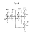
- Fig. 3 illustrates a conventional address buffer circuit of a semiconductor memory device which uses the buffer amplifier circuits of Fig. 1.
- the address buffer circuits of Fig. 3 comprises the first, the second and the third inverter circuits INV1, INV2 and INV3 which consist of MIS transistors Q3, Q4; Q5, Q6 and Q7, Q8, respectively, and each of which has the same circuit structure as that of the inverter circuit of Fig. 1.
- the address buffer circuit of Fig. 3 further comprises two output buffer amplifiers BA1 and BA2 which consist of MIS transistors Q9, Q10 and Q11, Q12, respectively and which output buffered address signals A o and A,, respectively.
- IBM Technical Disclosure Bulletin, Vol. 21, No. 7, December 1978, discloses a differential amplifier in which transistors whose gate electrodes receive respective input signals have further electrodes connected in common to an electrode of a further transistor whose gate electrode receives an output voltage of the amplifier.
- US-A-4 232 270 discloses a differential amplifier having two inverter stages in each of which one transistor is connected in series with a parallel connection of two further transistors. Of the two further transistors in each inverter stage, one receives an input signal at its gate electrode and the other receives the output of the other inverter stage. Both pairs of parallel- connected transistors are connected in common to an electrode of another transistor whose gate electrode receives the output of one of the inverter stages.
- the principal object of the present invention to provide a buffer amplifier circuit having a high operating speed.
- a buffer amplifier circuit comprising:
- Figure 4 illustrates an inverter type buffer amplifier circuit as an embodiment of the present invention.
- the buffer amplifier circuit of Figure 4 comprises a first inverter including a driver transistor Q13 and a load transistor Q14, a second inverter including a driver transistor Q15 and a load transistor Q16, and, a control transistor Q17.
- the source electrodes of the driver transistors Q13 and Q15 are commonly connected to the drain electrode of the control transistor Q17.
- Both the load transistors Q14 and Q16 are depletion type MIS transistors and the other transistors Q13, Q15 and Q17 are all enhancement type MIS transistors.
- the output terminal of the first inverter i.e., the drain electrode of the transistor Q13 is connected to the input terminal of the second inverter, i.e., the gate electrode of the transistor Q15.
- the output terminal of the second inverter i.e., the drain electrode of the transistor Q15 is connected to the gate electrode of the control transistor Q17.
- the operation of the buffer amplifier circuit of Figure 4 will now be described. Assume that the input signal A is to be changed from low level, e.g. 0.8 V, to high level, e.g. 2.0 V. In this case, as transistor Q13 is turned on, as the level of input signal A changes, the output signal B changes from high level, e.g. 5 V, towards low level, e.g. 0.7 V. As the transistor Q13 turns on the transistor Ql 5 turns off and the output signal C of the second inverter becomes higher, e.g. increases towards 5 V.
- low level e.g. 0.8 V
- high level e.g. 2.0 V.
- the output signal B changes from high level, e.g. 5 V
- low level e.g. 0.7 V.
- the transistor Q13 turns on the transistor Ql 5 turns off and the output signal C of the second inverter becomes higher, e.g. increases towards 5 V.
- the transistor Q17 is turned on and the potential D of the drain electrode of the transistor Q17 to which the source electrodes of the transistors Q13 and Q15 are connected becomes low, e.g. 0 V. Therefore, the input potential applied between the gate and source electrodes of the transistor Q13 is enlarged and the turning-on of the transistor Q13 is accelerated.
- the threshold potential of the input signal A can be determined by the gm ratio of the transistors 013 and Q14 to any appropriate value according to the potential levels of the input signal A without affecting the operating speed of the buffer amplifier circuit.
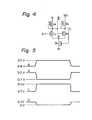
- Figure 6 illustrates an input-output characteristic of the buffer amplifier circuit of Figure 4. Since the potential D of the drain electrode of the control transistor Q17 changes in an opposite direction to that of the input signal A, the relation between the input signal A and the output signal B shows a hysteresis characteristic.
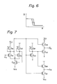
- Figure 7 illustrates an address buffer circuit which is used in a semiconductor memory device and which includes a buffer amplifier circuit according to the present invention.
- the address buffer circuit of Fig. 7 comprises an input buffer amplifier stage which includes MIS transistors Q18 through 022 and which has the same circuit structure as that of the buffer amplifier circuit of Figure 4, and an output buffer stage which includes MIS transistors Q23 through Q28 and which has the same circuit structure as that of the output buffer stage of the circuit of Fig. 3 including the inverter INV3 and the buffer amplifiers BA1 and BA2.
- the operation of the address buffer circuit is apparent from the above description, and therefore the explanation thereof is omitted here.
- the signal delay time of the output address signals A o and A o can be very small and the threshold potential of the input address signal A o can be selected to an approriate value according to the potential levels of the input address signal A o .
- the present invention it is possible to increase the operation speed of the inverter type buffer amplifier circuit, by using a simple circuitry including the control MIS transistor which enlarges the change of the input potential applied between the gate and the source electrodes of the driver transistor.
Landscapes
- Engineering & Computer Science (AREA)
- Computer Hardware Design (AREA)
- Physics & Mathematics (AREA)
- Computing Systems (AREA)
- General Engineering & Computer Science (AREA)
- Mathematical Physics (AREA)
- Power Engineering (AREA)
- Microelectronics & Electronic Packaging (AREA)
- Logic Circuits (AREA)
- Static Random-Access Memory (AREA)
Claims (7)
und gekennzeichnet durch
Applications Claiming Priority (2)
| Application Number | Priority Date | Filing Date | Title |
|---|---|---|---|
| JP159170/80 | 1980-11-12 | ||
| JP55159170A JPS5783930A (en) | 1980-11-12 | 1980-11-12 | Buffer circuit |
Publications (2)
| Publication Number | Publication Date |
|---|---|
| EP0052010A1 EP0052010A1 (de) | 1982-05-19 |
| EP0052010B1 true EP0052010B1 (de) | 1985-02-06 |
Family
ID=15687805
Family Applications (1)
| Application Number | Title | Priority Date | Filing Date |
|---|---|---|---|
| EP81305327A Expired EP0052010B1 (de) | 1980-11-12 | 1981-11-10 | Pufferverstärker und Adressenpufferschaltung mit einem solchen Pufferverstärker |
Country Status (5)
| Country | Link |
|---|---|
| US (1) | US4885479A (de) |
| EP (1) | EP0052010B1 (de) |
| JP (1) | JPS5783930A (de) |
| DE (1) | DE3168830D1 (de) |
| IE (1) | IE52401B1 (de) |
Families Citing this family (15)
| Publication number | Priority date | Publication date | Assignee | Title |
|---|---|---|---|---|
| US4456841A (en) * | 1982-02-05 | 1984-06-26 | International Business Machines Corporation | Field effect level sensitive circuit |
| JPS58137331A (ja) * | 1982-02-10 | 1983-08-15 | Nec Corp | インバ−タ回路 |
| US4835419A (en) * | 1987-10-30 | 1989-05-30 | International Business Machines Corporation | Source-follower emitter-coupled-logic receiver circuit |
| US4954730A (en) * | 1989-04-21 | 1990-09-04 | The Board Of Trustees Of The Leland Stanford Junior University | Complementary FET circuit having merged enhancement/depletion FET output |
| US5091662A (en) * | 1989-05-23 | 1992-02-25 | Texas Instruments Incorporated | High-speed low-power supply-independent TTL compatible input buffer |
| EP0461904A3 (en) * | 1990-06-14 | 1992-09-09 | Creative Integrated Systems, Inc. | An improved semiconductor read-only vlsi memory |
| US5235219A (en) * | 1992-04-01 | 1993-08-10 | Gte Laboratories Incorporated | Electrical circuitry with threshold control |
| US5491432A (en) * | 1992-08-07 | 1996-02-13 | Lsi Logic Corporation | CMOS Differential driver circuit for high offset ground |
| TW431067B (en) * | 1994-06-22 | 2001-04-21 | Ibm | Single source differential circuit |
| US5514982A (en) * | 1994-08-18 | 1996-05-07 | Harris Corporation | Low noise logic family |
| US6617892B2 (en) | 1998-09-18 | 2003-09-09 | Intel Corporation | Single ended interconnect systems |
| US6204696B1 (en) * | 1998-09-22 | 2001-03-20 | Intel Corporation | Domino circuits with high performance and high noise immunity |
| US6225826B1 (en) | 1998-12-23 | 2001-05-01 | Intel Corporation | Single ended domino compatible dual function generator circuits |
| US6137319A (en) * | 1999-04-30 | 2000-10-24 | Intel Corporation | Reference-free single ended clocked sense amplifier circuit |
| US6271713B1 (en) | 1999-05-14 | 2001-08-07 | Intel Corporation | Dynamic threshold source follower voltage driver circuit |
Family Cites Families (15)
| Publication number | Priority date | Publication date | Assignee | Title |
|---|---|---|---|---|
| JPS5318308B2 (de) * | 1973-03-05 | 1978-06-14 | ||
| US3950709A (en) * | 1974-10-01 | 1976-04-13 | General Instrument Corporation | Amplifier for random access computer memory |
| JPS5150550A (en) * | 1974-10-29 | 1976-05-04 | Tokyo Shibaura Electric Co | Fet zofukukairo |
| JPS5269545A (en) * | 1975-12-08 | 1977-06-09 | Hitachi Ltd | Oscillation circuit |
| US4071784A (en) * | 1976-11-12 | 1978-01-31 | Motorola, Inc. | MOS input buffer with hysteresis |
| US4079332A (en) * | 1976-11-22 | 1978-03-14 | Rockwell International Corporation | High gain differential amplifier |
| US4097772A (en) * | 1977-06-06 | 1978-06-27 | Motorola, Inc. | MOS switch with hysteresis |
| JPS6057156B2 (ja) * | 1978-05-24 | 1985-12-13 | 株式会社日立製作所 | 半導体メモリ装置 |
| US4242604A (en) * | 1978-08-10 | 1980-12-30 | National Semiconductor Corporation | MOS Input circuit with selectable stabilized trip voltage |
| JPS5526709A (en) * | 1978-08-14 | 1980-02-26 | Nec Corp | Amplifier circuit |
| JPS5824874B2 (ja) * | 1979-02-07 | 1983-05-24 | 富士通株式会社 | センス回路 |
| US4232270A (en) * | 1979-06-14 | 1980-11-04 | Rockwell International Corporation | High gain differential amplifier with positive feedback |
| US4274147A (en) * | 1979-09-04 | 1981-06-16 | Rockwell International Corporation | Static read only memory |
| JPS5748833A (en) * | 1980-09-05 | 1982-03-20 | Nec Corp | Gate circuit |
| JPH04101226A (ja) * | 1990-08-20 | 1992-04-02 | Nec Corp | インタープリタ型言語処理方式 |
-
1980
- 1980-11-12 JP JP55159170A patent/JPS5783930A/ja active Pending
-
1981
- 1981-11-10 DE DE8181305327T patent/DE3168830D1/de not_active Expired
- 1981-11-10 EP EP81305327A patent/EP0052010B1/de not_active Expired
- 1981-11-11 IE IE2646/81A patent/IE52401B1/en unknown
-
1984
- 1984-10-04 US US06/658,055 patent/US4885479A/en not_active Expired - Fee Related
Also Published As
| Publication number | Publication date |
|---|---|
| US4885479A (en) | 1989-12-05 |
| IE52401B1 (en) | 1987-10-14 |
| JPS5783930A (en) | 1982-05-26 |
| DE3168830D1 (en) | 1985-03-21 |
| EP0052010A1 (de) | 1982-05-19 |
| IE812646L (en) | 1982-05-12 |
Similar Documents
| Publication | Publication Date | Title |
|---|---|---|
| EP0052010B1 (de) | Pufferverstärker und Adressenpufferschaltung mit einem solchen Pufferverstärker | |
| US4985644A (en) | Output buffer semiconductor and method for controlling current flow in an output switching device | |
| KR940008718B1 (ko) | 직류 전류를 제거한 데이타 출력버퍼 | |
| US5448182A (en) | Driver circuit with self-adjusting impedance matching | |
| US5513140A (en) | Data output buffer | |
| KR930003540A (ko) | 노이즈가 억제되는 데이타 출력 버퍼 | |
| US5414379A (en) | Output buffer circuit for integrated circuit | |
| EP0174266B1 (de) | CMOS-Ausgangspuffer | |
| US5173627A (en) | Circuit for outputting a data signal following an output enable command signal | |
| KR910003603B1 (ko) | 쉬미트입력형 반도체집적회로 | |
| US5940330A (en) | Synchronous memory device having a plurality of clock input buffers | |
| KR100264076B1 (ko) | 데이타 출력 드라이버 전류를 증가시킨 디램 | |
| KR100275956B1 (ko) | 데이타 입출력 포트 | |
| KR940003399B1 (ko) | 저잡음 데이타 출력 버퍼 | |
| KR100190303B1 (ko) | 반도체 메모리소자의 출력 버퍼 | |
| KR960013854B1 (ko) | 데이타 출력버퍼 | |
| KR970005571B1 (ko) | 데이타 출력버퍼 | |
| KR100239717B1 (ko) | 데이타 출력버퍼 | |
| JPH0879046A (ja) | 出力回路 | |
| KR940008141B1 (ko) | 어드레스 버퍼 회로 | |
| JP3639050B2 (ja) | 入力回路及び半導体装置 | |
| JPH0537305A (ja) | ラツチ回路 | |
| KR100289382B1 (ko) | 데이터출력회로 | |
| KR910003790B1 (ko) | 출력 버퍼 회로 | |
| KR0120586B1 (ko) | 데이타 출력버퍼 |
Legal Events
| Date | Code | Title | Description |
|---|---|---|---|
| PUAI | Public reference made under article 153(3) epc to a published international application that has entered the european phase |
Free format text: ORIGINAL CODE: 0009012 |
|
| AK | Designated contracting states |
Designated state(s): DE FR GB NL |
|
| 17P | Request for examination filed |
Effective date: 19821110 |
|
| GRAA | (expected) grant |
Free format text: ORIGINAL CODE: 0009210 |
|
| AK | Designated contracting states |
Designated state(s): DE FR GB NL |
|
| REF | Corresponds to: |
Ref document number: 3168830 Country of ref document: DE Date of ref document: 19850321 |
|
| ET | Fr: translation filed | ||
| PLBE | No opposition filed within time limit |
Free format text: ORIGINAL CODE: 0009261 |
|
| STAA | Information on the status of an ep patent application or granted ep patent |
Free format text: STATUS: NO OPPOSITION FILED WITHIN TIME LIMIT |
|
| 26N | No opposition filed | ||
| PGFP | Annual fee paid to national office [announced via postgrant information from national office to epo] |
Ref country code: NL Payment date: 19871130 Year of fee payment: 7 |
|
| PGFP | Annual fee paid to national office [announced via postgrant information from national office to epo] |
Ref country code: DE Payment date: 19890126 Year of fee payment: 8 |
|
| PG25 | Lapsed in a contracting state [announced via postgrant information from national office to epo] |
Ref country code: GB Effective date: 19891110 |
|
| PG25 | Lapsed in a contracting state [announced via postgrant information from national office to epo] |
Ref country code: NL Effective date: 19900601 |
|
| GBPC | Gb: european patent ceased through non-payment of renewal fee | ||
| NLV4 | Nl: lapsed or anulled due to non-payment of the annual fee | ||
| PG25 | Lapsed in a contracting state [announced via postgrant information from national office to epo] |
Ref country code: FR Effective date: 19900731 |
|
| PG25 | Lapsed in a contracting state [announced via postgrant information from national office to epo] |
Ref country code: DE Effective date: 19900801 |
|
| REG | Reference to a national code |
Ref country code: FR Ref legal event code: ST |