EP0022176B1 - Module pour plaquettes à circuit intégré - Google Patents
Module pour plaquettes à circuit intégré Download PDFInfo
- Publication number
- EP0022176B1 EP0022176B1 EP80103083A EP80103083A EP0022176B1 EP 0022176 B1 EP0022176 B1 EP 0022176B1 EP 80103083 A EP80103083 A EP 80103083A EP 80103083 A EP80103083 A EP 80103083A EP 0022176 B1 EP0022176 B1 EP 0022176B1
- Authority
- EP
- European Patent Office
- Prior art keywords
- conductors
- substrate
- stack
- circuit chips
- module according
- Prior art date
- Legal status (The legal status is an assumption and is not a legal conclusion. Google has not performed a legal analysis and makes no representation as to the accuracy of the status listed.)
- Expired
Links
Images


Classifications
-
- H—ELECTRICITY
- H05—ELECTRIC TECHNIQUES NOT OTHERWISE PROVIDED FOR
- H05K—PRINTED CIRCUITS; CASINGS OR CONSTRUCTIONAL DETAILS OF ELECTRIC APPARATUS; MANUFACTURE OF ASSEMBLAGES OF ELECTRICAL COMPONENTS
- H05K1/00—Printed circuits
- H05K1/02—Details
- H05K1/14—Structural association of two or more printed circuits
- H05K1/144—Stacked arrangements of planar printed circuit boards
-
- H—ELECTRICITY
- H01—ELECTRIC ELEMENTS
- H01L—SEMICONDUCTOR DEVICES NOT COVERED BY CLASS H10
- H01L23/00—Details of semiconductor or other solid state devices
- H01L23/58—Structural electrical arrangements for semiconductor devices not otherwise provided for, e.g. in combination with batteries
- H01L23/64—Impedance arrangements
- H01L23/642—Capacitive arrangements
-
- H—ELECTRICITY
- H01—ELECTRIC ELEMENTS
- H01L—SEMICONDUCTOR DEVICES NOT COVERED BY CLASS H10
- H01L24/00—Arrangements for connecting or disconnecting semiconductor or solid-state bodies; Methods or apparatus related thereto
- H01L24/01—Means for bonding being attached to, or being formed on, the surface to be connected, e.g. chip-to-package, die-attach, "first-level" interconnects; Manufacturing methods related thereto
- H01L24/10—Bump connectors ; Manufacturing methods related thereto
- H01L24/15—Structure, shape, material or disposition of the bump connectors after the connecting process
- H01L24/16—Structure, shape, material or disposition of the bump connectors after the connecting process of an individual bump connector
-
- H—ELECTRICITY
- H05—ELECTRIC TECHNIQUES NOT OTHERWISE PROVIDED FOR
- H05K—PRINTED CIRCUITS; CASINGS OR CONSTRUCTIONAL DETAILS OF ELECTRIC APPARATUS; MANUFACTURE OF ASSEMBLAGES OF ELECTRICAL COMPONENTS
- H05K7/00—Constructional details common to different types of electric apparatus
- H05K7/02—Arrangements of circuit components or wiring on supporting structure
- H05K7/06—Arrangements of circuit components or wiring on supporting structure on insulating boards, e.g. wiring harnesses
-
- H—ELECTRICITY
- H05—ELECTRIC TECHNIQUES NOT OTHERWISE PROVIDED FOR
- H05K—PRINTED CIRCUITS; CASINGS OR CONSTRUCTIONAL DETAILS OF ELECTRIC APPARATUS; MANUFACTURE OF ASSEMBLAGES OF ELECTRICAL COMPONENTS
- H05K7/00—Constructional details common to different types of electric apparatus
- H05K7/02—Arrangements of circuit components or wiring on supporting structure
- H05K7/12—Resilient or clamping means for holding component to structure
-
- H—ELECTRICITY
- H01—ELECTRIC ELEMENTS
- H01L—SEMICONDUCTOR DEVICES NOT COVERED BY CLASS H10
- H01L2224/00—Indexing scheme for arrangements for connecting or disconnecting semiconductor or solid-state bodies and methods related thereto as covered by H01L24/00
- H01L2224/01—Means for bonding being attached to, or being formed on, the surface to be connected, e.g. chip-to-package, die-attach, "first-level" interconnects; Manufacturing methods related thereto
- H01L2224/10—Bump connectors; Manufacturing methods related thereto
- H01L2224/15—Structure, shape, material or disposition of the bump connectors after the connecting process
- H01L2224/16—Structure, shape, material or disposition of the bump connectors after the connecting process of an individual bump connector
- H01L2224/161—Disposition
- H01L2224/16151—Disposition the bump connector connecting between a semiconductor or solid-state body and an item not being a semiconductor or solid-state body, e.g. chip-to-substrate, chip-to-passive
- H01L2224/16221—Disposition the bump connector connecting between a semiconductor or solid-state body and an item not being a semiconductor or solid-state body, e.g. chip-to-substrate, chip-to-passive the body and the item being stacked
- H01L2224/16225—Disposition the bump connector connecting between a semiconductor or solid-state body and an item not being a semiconductor or solid-state body, e.g. chip-to-substrate, chip-to-passive the body and the item being stacked the item being non-metallic, e.g. insulating substrate with or without metallisation
-
- H—ELECTRICITY
- H01—ELECTRIC ELEMENTS
- H01L—SEMICONDUCTOR DEVICES NOT COVERED BY CLASS H10
- H01L2924/00—Indexing scheme for arrangements or methods for connecting or disconnecting semiconductor or solid-state bodies as covered by H01L24/00
- H01L2924/01—Chemical elements
- H01L2924/01014—Silicon [Si]
-
- H—ELECTRICITY
- H01—ELECTRIC ELEMENTS
- H01L—SEMICONDUCTOR DEVICES NOT COVERED BY CLASS H10
- H01L2924/00—Indexing scheme for arrangements or methods for connecting or disconnecting semiconductor or solid-state bodies as covered by H01L24/00
- H01L2924/01—Chemical elements
- H01L2924/0102—Calcium [Ca]
-
- H—ELECTRICITY
- H01—ELECTRIC ELEMENTS
- H01L—SEMICONDUCTOR DEVICES NOT COVERED BY CLASS H10
- H01L2924/00—Indexing scheme for arrangements or methods for connecting or disconnecting semiconductor or solid-state bodies as covered by H01L24/00
- H01L2924/01—Chemical elements
- H01L2924/01068—Erbium [Er]
-
- H—ELECTRICITY
- H01—ELECTRIC ELEMENTS
- H01L—SEMICONDUCTOR DEVICES NOT COVERED BY CLASS H10
- H01L2924/00—Indexing scheme for arrangements or methods for connecting or disconnecting semiconductor or solid-state bodies as covered by H01L24/00
- H01L2924/10—Details of semiconductor or other solid state devices to be connected
- H01L2924/11—Device type
- H01L2924/12—Passive devices, e.g. 2 terminal devices
- H01L2924/1203—Rectifying Diode
- H01L2924/12033—Gunn diode
-
- H—ELECTRICITY
- H01—ELECTRIC ELEMENTS
- H01L—SEMICONDUCTOR DEVICES NOT COVERED BY CLASS H10
- H01L2924/00—Indexing scheme for arrangements or methods for connecting or disconnecting semiconductor or solid-state bodies as covered by H01L24/00
- H01L2924/10—Details of semiconductor or other solid state devices to be connected
- H01L2924/11—Device type
- H01L2924/12—Passive devices, e.g. 2 terminal devices
- H01L2924/1204—Optical Diode
- H01L2924/12042—LASER
-
- H—ELECTRICITY
- H01—ELECTRIC ELEMENTS
- H01L—SEMICONDUCTOR DEVICES NOT COVERED BY CLASS H10
- H01L2924/00—Indexing scheme for arrangements or methods for connecting or disconnecting semiconductor or solid-state bodies as covered by H01L24/00
- H01L2924/10—Details of semiconductor or other solid state devices to be connected
- H01L2924/11—Device type
- H01L2924/14—Integrated circuits
-
- H—ELECTRICITY
- H01—ELECTRIC ELEMENTS
- H01L—SEMICONDUCTOR DEVICES NOT COVERED BY CLASS H10
- H01L2924/00—Indexing scheme for arrangements or methods for connecting or disconnecting semiconductor or solid-state bodies as covered by H01L24/00
- H01L2924/30—Technical effects
- H01L2924/301—Electrical effects
- H01L2924/3025—Electromagnetic shielding
Definitions
- the invention relates to a module for circuit chips, the power supply of which takes place via structures of parallel current conductors with a high mutual capacitance, as stated in the preamble of claim 1 and described in US Pat. No. 3,949,274.
- modules for combining circuit chips including those with a chip carrier.
- circuit chips micro module
- Several parallel circuit boards are stacked on top of each other. These are also parallel to the surface on which the chip contacts are electrically connected to connection points.
- the printed circuit boards have large areas and dielectric material lies between them, so that this structure includes high mutual capacities.
- their disadvantage lies in the large number of connections between the printed circuit boards and the chips, the manufacture of which is complicated. The reason for this is that many connections have to be made across parallel plates to the connection points on the top surface of the chip carrier.
- This is mainly possible thanks to the high capacitance between the conductors and very close to the chips, although several supply conductors have to be connected to each chip.
- the interference suppression must also be effective for fast-switching computing devices and at the same time the module must be simple and easy to manufacture.
- the chip carrier module 7 of FIG. 1 has a substrate 22 as a mechanical base on which the entire structure of the module is built.
- the substrate 22 can perform the important electrical function of a ground and reference level.
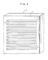
- the substrate 22 is shown in a perspective view in FIG. 3 and shows ten milled slots 23 which break through its thickness.
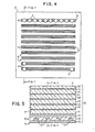
- a stack 10 of stacked printed circuit boards 11 with dielectric insulation layers 13 and a shielded flat cable 24, as shown in FIG. 5, is introduced into each slot 23.
- Each stack 10 comprises twelve layered printed circuit boards 11 except for the shielded flat conductor 24 and extends through the slot 23.
- the printed circuit boards 11 are connected to various power supply rails 30 by means of staggered connecting lugs 21, the majority of which are not shown to simplify the illustration.
- These stacks 10 are firmly embedded in the substrate 22 and are stuck therein in a rigid, mechanical connection. However, they are electrically insulated from direct current.
- the large parallel surfaces of the printed circuit boards 11 result in very large mutual capacitance values which are associated with the lowest values of inductive coupling.
- the individual stacks 10 are individually connected to different power supply rails 30 depending on the requirements of the chips 8.
- Contact layers 12 are preferred on the flat, metallic surface 18 of the substrate, which has been made flat by machining as applied in the form of connecting lines 41, in thin-film technology and in several layers, as clearly shown in FIG. 7 in detail.
- the substrate 22 of FIG. 3 is made from a metal plate about 90 mm square and 12 mm thick, and ten slots 23 have been milled through. Each slot 23 has two surfaces which are applied measured from a reference position with an accuracy of 1 mm 2,5-10-. The slots are approximately 3.8 mm wide and are centered at a distance of 7.6 mm side by side.
- the chips 8 are arranged in an arrangement 10 ⁇ 10 pieces on the surface of the substrate, the simplified illustration in FIG. 1 only showing two rows with a smaller number. 4 is a much better view of the actually preferred embodiment.
- the flat conductor cable 24 is fastened in the corner 16, which is formed by the two surfaces milled with great accuracy.
- the conductor contained in the cable are also set to 2,5-10- 1 mm accuracy.
- the individual circuit boards 11 are approximately 0.25 mm thick and have. an insulation 13 of about 1.2 x 10 -2 mm thick.
- the chip connection contacts (42 in FIG. 7) with solder balls (C-4) have a center-to-center distance on the chip 8 of, for example, 0.19 mm.
- the chip is rotated through 45 °, then about half of the C-4 contact points lie exactly above the printed circuit boards 11, so that, if desired, a direct connection between the solder ball contacts and the upper edges 31 of the printed circuit boards 11 can be established.
- the flat conductor cable 24, however, is connected to the thin-film contact layers of Fig. 7, dieals allow tolerance for aligning a multiple of 2.5 x 10 -2 mm.
- FIG. 5 shows the enlargement of a corner of a slot 23, which is formed by the two side surfaces which have been created precisely during processing and with respect to which the position of the conductor stack 10 is determined and the latter is fastened. This also determines the exact position of the signal conductors 27 so that they can be connected to the contact layers 12.
- the conductors are embedded in the insulation 26 in the flat conductor cable 24 and lie between two shielding layers 25 and 28. Some or all of the circuit boards of the power supply must be insulated from the substrate 22, as well as from one another, by a layer 14 or layers 13. Such flat conductor cables 24 and the methods for connecting them to other cables and plugs are known.
- the conductor stacks 10 can be cemented to the substrate 22 by glazing or by other means.
- a ribbon cable 33 is connected to one end of the flat conductor cable 24 and then connected to a signal distribution plate 35. This has connecting pins 36 on its underside.
- the ribbon cables 33 used can either be rigid or flexible.
- the metal of the conductors can be copper or a material that is matched in terms of expansion coefficient, as will be discussed.
- connection lugs 21 for connection to a direct current rail 30.
- connection lugs 15 can be present, which are used for connection to decoupling capacitors at the lower end of the printed circuit boards.
- a set of four printed circuit boards 11 V1 to V4, which alternate as shown in FIG. 5, is preferably arranged.
- the terminal lugs 15 and 21 of each type of printed circuit board 11 would each lie in a specific position.
- the flat conductor cable 24 would also end in a soldered connection and transition into a flexible ribbon cable of the usual type. If the latter is sufficiently flexible, as shown in FIG. 6, it could be bent through 90 ° and connected to a printed circuit board.
- This arrangement results in approximately 20 cm 2 of conductor area per chip and per busbar 30.
- This enables an insulation thickness of 10-25 ⁇ m to be used, which is easy to manufacture and at the same time results in sufficient capacitance between the plates in order to prevent the undesired, high-frequency settling processes at the power supply points to suppress the chips 8.
- the printed circuit boards 11 have prefabricated surfaces, so that the opening of a pinhole of the insulation layer 13 does not necessarily cause a short circuit. This would be the case if the structure were built up by successive and alternating application of conductor and insulation layers, for example by vacuum deposition.
- the decoupling capacitors 32 shown are added to the capacitances of approximately 1 ⁇ F that are present between the printed circuit boards 11 separated by the dielectric 13, and act primarily against slow transient processes. However, it also results in an attenuation of higher frequencies.
- the latter In order to be able to guide about 160-200 signal conductors in a ribbon cable 33, the latter are arranged at a center-to-center distance of 0.5 mm. Under these circumstances, the connections can be made easily, for example by flow soldering.
- the chip carrier module 7 should be thermally adapted to the chips 8. Therefore, the use of molybdenum for the substrate 22 has been considered. However, this is based on the assumption that the carrier reaches the same temperature as the silicon, but this only applies to thermally poor conductors. 6, a coolant line 40 leads into the substrate 22. 22 coolant channels must therefore be produced in the substrate. The temperature rise can be controlled, which enables the use of metals with a large expansion coefficient, such as copper or brass, which are easier to machine. As an alternative, the metal block can also be cooled to keep the expansion approximately zero. All connections with a chip 8 can be made via the thin con Clock layers 12 are performed. If each of these lines is provided with a bend of at least 90 °, the thermal expansion of silicon of approx. 11 m can easily be absorbed by the flexibility of the copper line and the organic insulation. So there is no stress on the C-4 contact points and no fatigue problem.
- FIG. 7 shows the layout of the structure of actual connection lines which are used, enclosed in contact layers 12, and, as shown in FIG. 6, are applied to the flat metal surface.
- the chip 8 rests on the contact layer 12. It is externally supported by C-4 solder balls 42 and connected to the same solder balls 43, which sit on layer bushings 44 and 45. The latter have been prepared in conical openings in the uppermost of the contact layers 12.
- the feedthrough 45 connects via a V-shaped conductor down to an upper, lossy transmission line 46. This line extends, via a further feedthrough 47, beyond the right edge of the illustration to one or more feedthroughs which are connected to other chips and are similar. Below line 46, another line 48 is also connected to bushing 47.
- the lossy line 48 has been drawn directly below the line 46, although it would preferably continue perpendicular to the plane of the drawing. Below this, however, would lie the line 50, which is connected to the line 48 via the feedthrough 49, and it would preferably, but not necessarily, extend parallel to the line 46, as shown.
- This arrangement would therefore be suitable for a system arranged according to right-angled x, y coordinates, lines in the x direction being at the level of the line 48, and those in the y direction being at the level of the line 50.
- the top level, including line 46 would be a layer for performing tests and technical changes.
- openings 66 only one of which is shown, could serve e.g. using a laser beam, to cut connections in a known manner, etc.
- the transmission lines 56, 58 and 60 and the bushings 57, 59 and 61 connect a C-4 solder ball 43 to the circuit board V1.
- the lines 46, 48 and 50, as well as 56, 58 and 60, are embedded in a dielectric 55, which preferably consists of a polyimide, plastic or glass and at the same time insulates and supports.
- the lowermost line 50 is in electrical contact with the conductor 27 of the flat conductor cable 24 via the bushing 51 (see FIG. 5).
- the lines 46, 48 and 50, with respect to the ground plane 22, represent individual, lossy strip lines which are designed to transmit signal pulses at high speed and at the same time to attenuate reflections.
- the circuit board V1 which is used as a feedthrough through the surface of the substrate 22, supplies the lines 56, 58, 60 etc. with current, thanks to their layer structure, via a minimum of inductance. It can therefore carry both input and output signals for the block. With this arrangement, higher wiring density for the lines 46, 48, 50, as well as 56, 58 and 60, can be achieved, since these can be made very narrow.
- the thin film structure of the line enables the current to be passed on via the substrate 22 and this line with almost no additional inductance.
- the lines 46, 48, 50, etc. taken together with the ground and reference plane of the substrate 22, as shown in FIG. 7, form thin-layer transmission lines of the so-called strip lines type.
- These devices are mass-produced using the conventional thin film deposition technique using photoresist and photolithographic masking used in the manufacture of VLSI chips.
- the precipitate can also be vacuumed by evaporation, spraying, or by galvanic plating, etc. can be achieved, which greatly facilitates the production of a module 7.
- the metallizations and leadthroughs are built up in successive layers, layer by layer and step by step. If, for example, the metallization of the line 50 is applied in the x direction to a layer of dielectric 55, this happens after an opening for a bushing has been made in a previous step. Then the metallization 50 is covered with further dielectric material 55 and the metallization 48 is applied in the y direction, etc.
- the embodiment shown in the drawings shows only a homogeneous, metallic block for the module with substrate 22 and flat conductor cable 24. Obviously, however, a metal-coated insulator can also be used as substrate 22. In addition, the flexibility of the arrangement of the contact layers 12 also allows conventional pin contacts to be used to couple out signals from the module 7.
Claims (6)
Applications Claiming Priority (2)
| Application Number | Priority Date | Filing Date | Title |
|---|---|---|---|
| US06/053,660 US4237522A (en) | 1979-06-29 | 1979-06-29 | Chip package with high capacitance, stacked vlsi/power sheets extending through slots in substrate |
| US53660 | 1979-06-29 |
Publications (2)
| Publication Number | Publication Date |
|---|---|
| EP0022176A1 EP0022176A1 (fr) | 1981-01-14 |
| EP0022176B1 true EP0022176B1 (fr) | 1983-01-12 |
Family
ID=21985743
Family Applications (1)
| Application Number | Title | Priority Date | Filing Date |
|---|---|---|---|
| EP80103083A Expired EP0022176B1 (fr) | 1979-06-29 | 1980-06-03 | Module pour plaquettes à circuit intégré |
Country Status (11)
| Country | Link |
|---|---|
| US (1) | US4237522A (fr) |
| EP (1) | EP0022176B1 (fr) |
| JP (1) | JPS58187B2 (fr) |
| BR (1) | BR8004063A (fr) |
| CA (1) | CA1137646A (fr) |
| DE (1) | DE3061605D1 (fr) |
| DK (1) | DK277580A (fr) |
| ES (1) | ES8102417A1 (fr) |
| FI (1) | FI802059A (fr) |
| IT (1) | IT1150994B (fr) |
| NO (1) | NO801801L (fr) |
Cited By (1)
| Publication number | Priority date | Publication date | Assignee | Title |
|---|---|---|---|---|
| DE4237083A1 (de) * | 1992-11-03 | 1994-05-05 | Diehl Gmbh & Co | Anordnung von miteinander verschalteten Baugruppen |
Families Citing this family (26)
| Publication number | Priority date | Publication date | Assignee | Title |
|---|---|---|---|---|
| US4295183A (en) * | 1979-06-29 | 1981-10-13 | International Business Machines Corporation | Thin film metal package for LSI chips |
| US4281361A (en) * | 1980-03-17 | 1981-07-28 | The United States Of America As Represented By The Secretary Of The Navy | Simplified multilayer circuit board |
| US4328530A (en) * | 1980-06-30 | 1982-05-04 | International Business Machines Corporation | Multiple layer, ceramic carrier for high switching speed VLSI chips |
| US4349862A (en) * | 1980-08-11 | 1982-09-14 | International Business Machines Corporation | Capacitive chip carrier and multilayer ceramic capacitors |
| US4453176A (en) * | 1981-12-31 | 1984-06-05 | International Business Machines Corporation | LSI Chip carrier with buried repairable capacitor with low inductance leads |
| JPS6012095U (ja) * | 1983-06-29 | 1985-01-26 | 黒崎窯業株式会社 | 熱交換器 |
| US4535388A (en) * | 1984-06-29 | 1985-08-13 | International Business Machines Corporation | High density wired module |
| JPS6156493A (ja) * | 1984-08-28 | 1986-03-22 | 日本電気株式会社 | 多層回路基板の電源配線構造 |
| US4945399A (en) * | 1986-09-30 | 1990-07-31 | International Business Machines Corporation | Electronic package with integrated distributed decoupling capacitors |
| US4744008A (en) * | 1986-11-18 | 1988-05-10 | International Business Machines Corporation | Flexible film chip carrier with decoupling capacitors |
| US4907068A (en) * | 1987-01-21 | 1990-03-06 | Siemens Aktiengesellschaft | Semiconductor arrangement having at least one semiconductor body |
| US4868634A (en) * | 1987-03-13 | 1989-09-19 | Citizen Watch Co., Ltd. | IC-packaged device |
| US4855809A (en) * | 1987-11-24 | 1989-08-08 | Texas Instruments Incorporated | Orthogonal chip mount system module and method |
| US5025306A (en) * | 1988-08-09 | 1991-06-18 | Texas Instruments Incorporated | Assembly of semiconductor chips |
| US5027253A (en) * | 1990-04-09 | 1991-06-25 | Ibm Corporation | Printed circuit boards and cards having buried thin film capacitors and processing techniques for fabricating said boards and cards |
| US5343366A (en) * | 1992-06-24 | 1994-08-30 | International Business Machines Corporation | Packages for stacked integrated circuit chip cubes |
| JPH0828244B2 (ja) * | 1993-04-28 | 1996-03-21 | 日本電気株式会社 | マルチチップパッケージの給電構造 |
| US5765279A (en) * | 1995-05-22 | 1998-06-16 | Fujitsu Limited | Methods of manufacturing power supply distribution structures for multichip modules |
| US5657537A (en) * | 1995-05-30 | 1997-08-19 | General Electric Company | Method for fabricating a stack of two dimensional circuit modules |
| US7321485B2 (en) | 1997-04-08 | 2008-01-22 | X2Y Attenuators, Llc | Arrangement for energy conditioning |
| US7336468B2 (en) | 1997-04-08 | 2008-02-26 | X2Y Attenuators, Llc | Arrangement for energy conditioning |
| US9054094B2 (en) | 1997-04-08 | 2015-06-09 | X2Y Attenuators, Llc | Energy conditioning circuit arrangement for integrated circuit |
| US6657313B1 (en) * | 1999-01-19 | 2003-12-02 | International Business Machines Corporation | Dielectric interposer for chip to substrate soldering |
| JP2008535207A (ja) | 2005-03-01 | 2008-08-28 | エックストゥーワイ アテニュエイターズ,エルエルシー | 共平面導体を有する調整器 |
| US7983024B2 (en) * | 2007-04-24 | 2011-07-19 | Littelfuse, Inc. | Fuse card system for automotive circuit protection |
| US9275966B2 (en) * | 2012-06-21 | 2016-03-01 | Freescale Semiconductor, Inc. | Semiconductor device apparatus and assembly with opposite die orientations |
Family Cites Families (14)
| Publication number | Priority date | Publication date | Assignee | Title |
|---|---|---|---|---|
| US2995686A (en) * | 1959-03-02 | 1961-08-08 | Sylvania Electric Prod | Microelectronic circuit module |
| US3243661A (en) * | 1963-06-25 | 1966-03-29 | United Aircraft Corp | Enhanced micro-modules |
| US3312870A (en) * | 1964-03-13 | 1967-04-04 | Hughes Aircraft Co | Electrical transmission system |
| US3353070A (en) * | 1965-12-13 | 1967-11-14 | Bunker Ramo | Molded sandwich electrical connector with improved connector pins and encapsulating structure |
| US3437882A (en) * | 1966-01-14 | 1969-04-08 | Texas Instruments Inc | Circuit board structure with interconnecting means |
| FR1520294A (fr) * | 1966-04-25 | 1968-04-05 | Texas Instruments Inc | Perfectionnements aux réseaux de circuits intégrés et à leurs procédés de fabrication |
| US3436604A (en) * | 1966-04-25 | 1969-04-01 | Texas Instruments Inc | Complex integrated circuit array and method for fabricating same |
| US3418535A (en) * | 1967-01-23 | 1968-12-24 | Elco Corp | Interconnection matrix for dual-in-line packages |
| US3522485A (en) * | 1967-11-21 | 1970-08-04 | Automatic Radio Mfg Co | Modular circuit construction |
| GB1152809A (en) * | 1968-05-07 | 1969-05-21 | Standard Telephones Cables Ltd | Electric Circuit Assembly |
| US3671812A (en) * | 1970-07-01 | 1972-06-20 | Martin Marietta Corp | High density packaging of electronic components in three-dimensional modules |
| GB1278380A (en) * | 1970-08-13 | 1972-06-21 | Standard Telephones Cables Ltd | Electrical circuit assembly |
| US3949274A (en) * | 1974-05-30 | 1976-04-06 | International Business Machines Corporation | Packaging and interconnection for superconductive circuitry |
| US4109298A (en) * | 1976-07-26 | 1978-08-22 | Texas Instruments Incorporated | Connector with printed wiring board structure |
-
1979
- 1979-06-29 US US06/053,660 patent/US4237522A/en not_active Expired - Lifetime
-
1980
- 1980-04-14 CA CA000349745A patent/CA1137646A/fr not_active Expired
- 1980-05-20 JP JP55066054A patent/JPS58187B2/ja not_active Expired
- 1980-06-03 EP EP80103083A patent/EP0022176B1/fr not_active Expired
- 1980-06-03 DE DE8080103083T patent/DE3061605D1/de not_active Expired
- 1980-06-17 NO NO801801A patent/NO801801L/no unknown
- 1980-06-23 IT IT22957/80A patent/IT1150994B/it active
- 1980-06-25 ES ES492742A patent/ES8102417A1/es not_active Expired
- 1980-06-27 BR BR8004063A patent/BR8004063A/pt unknown
- 1980-06-27 DK DK277580A patent/DK277580A/da not_active Application Discontinuation
- 1980-06-27 FI FI802059A patent/FI802059A/fi not_active Application Discontinuation
Cited By (2)
| Publication number | Priority date | Publication date | Assignee | Title |
|---|---|---|---|---|
| DE4237083A1 (de) * | 1992-11-03 | 1994-05-05 | Diehl Gmbh & Co | Anordnung von miteinander verschalteten Baugruppen |
| DE4237083C2 (de) * | 1992-11-03 | 2002-11-28 | Diehl Stiftung & Co | Anordnung von miteinander verschalteten Baugruppen |
Also Published As
| Publication number | Publication date |
|---|---|
| BR8004063A (pt) | 1981-01-21 |
| EP0022176A1 (fr) | 1981-01-14 |
| DE3061605D1 (en) | 1983-02-17 |
| JPS567458A (en) | 1981-01-26 |
| IT1150994B (it) | 1986-12-17 |
| NO801801L (no) | 1980-12-30 |
| US4237522A (en) | 1980-12-02 |
| ES492742A0 (es) | 1980-12-16 |
| IT8022957A0 (it) | 1980-06-23 |
| FI802059A (fi) | 1980-12-30 |
| JPS58187B2 (ja) | 1983-01-05 |
| CA1137646A (fr) | 1982-12-14 |
| ES8102417A1 (es) | 1980-12-16 |
| DK277580A (da) | 1980-12-30 |
Similar Documents
| Publication | Publication Date | Title |
|---|---|---|
| EP0022176B1 (fr) | Module pour plaquettes à circuit intégré | |
| EP0035093B1 (fr) | Empaquetage pour plusieurs pastilles semiconductrices à commutation rapide | |
| DE1591199C2 (fr) | ||
| EP0221399B1 (fr) | Module semi-conducteur de puissance | |
| DE2554965C2 (fr) | ||
| DE4325668C2 (de) | Mehrebenen-Verdrahtungssubstrat und dieses verwendende Halbleiteranordnung | |
| DE2542518C3 (fr) | ||
| DE2752438C2 (de) | Träger für eine integrierte Schaltung | |
| DE69632003T2 (de) | Starre-flexible Leiterplatte mit einer Öffnung für einen isolierten Montierungsbereich | |
| DE102014111829B4 (de) | Ein Halbleitermodul und ein Verfahren zu dessen Fabrikation durch erweiterte Einbettungstechnologien | |
| DE10234951B4 (de) | Verfahren zur Herstellung von Halbleiterschaltungsmodulen | |
| DE4027072C2 (de) | Halbleiteranordnung | |
| DE4015788C2 (de) | Baugruppe | |
| DE3911711A1 (de) | Modul-aufbau mit integriertem halbleiterchip und chiptraeger | |
| DE2920564A1 (de) | Duennfilm-leitungen fuer elektronische schaltkreise | |
| WO2005091366A2 (fr) | Module a semi-conducteur avec substrat de couplage et procede de realisation | |
| DE102018123837B4 (de) | Halbleiterpackage und Halbleitermodul mit demselben | |
| DE102004039906A1 (de) | Verfahren zur Herstellung eines elektronischen Bauelements sowie ein elektronisches Bauelement mit mindestens zwei integrierten Bausteinen | |
| DE112015005031T5 (de) | Substrate und verfahren zu ihrer herstellung | |
| DE19517367A1 (de) | Verfahren zum Anschließen der Ausgangsbereiche eines Chips mit integrierter Schaltung und so erhaltener Mehr-Chip-Modul | |
| EP0738008B1 (fr) | Module à semi-conducteur de puissance | |
| EP0531984A1 (fr) | Circuit électronique pour des composants semi-conducteurs de puissance | |
| DE2317404A1 (de) | Bauelementplaettchen fuer eine vielschichtige elektrische schaltungsanordnung | |
| DE102017202329A1 (de) | Multilayer-Leiterplatte sowie elektronische Anordnung mit einer solchen | |
| DE19648492A1 (de) | Multi-Chip-Modul |
Legal Events
| Date | Code | Title | Description |
|---|---|---|---|
| PUAI | Public reference made under article 153(3) epc to a published international application that has entered the european phase |
Free format text: ORIGINAL CODE: 0009012 |
|
| AK | Designated contracting states |
Designated state(s): BE DE FR GB SE |
|
| 17P | Request for examination filed |
Effective date: 19810205 |
|
| GRAA | (expected) grant |
Free format text: ORIGINAL CODE: 0009210 |
|
| AK | Designated contracting states |
Designated state(s): BE DE FR GB SE |
|
| REF | Corresponds to: |
Ref document number: 3061605 Country of ref document: DE Date of ref document: 19830217 |
|
| ET | Fr: translation filed | ||
| PGFP | Annual fee paid to national office [announced via postgrant information from national office to epo] |
Ref country code: BE Payment date: 19830630 Year of fee payment: 4 |
|
| PG25 | Lapsed in a contracting state [announced via postgrant information from national office to epo] |
Ref country code: BE Effective date: 19840630 |
|
| PGFP | Annual fee paid to national office [announced via postgrant information from national office to epo] |
Ref country code: SE Payment date: 19840630 Year of fee payment: 5 |
|
| BERE | Be: lapsed |
Owner name: INTERNATIONAL BUSINESS MACHINES CORP. Effective date: 19840603 |
|
| PG25 | Lapsed in a contracting state [announced via postgrant information from national office to epo] |
Ref country code: SE Effective date: 19860604 |
|
| PGFP | Annual fee paid to national office [announced via postgrant information from national office to epo] |
Ref country code: GB Payment date: 19900516 Year of fee payment: 11 |
|
| PGFP | Annual fee paid to national office [announced via postgrant information from national office to epo] |
Ref country code: FR Payment date: 19900529 Year of fee payment: 11 |
|
| PGFP | Annual fee paid to national office [announced via postgrant information from national office to epo] |
Ref country code: DE Payment date: 19900707 Year of fee payment: 11 |
|
| PG25 | Lapsed in a contracting state [announced via postgrant information from national office to epo] |
Ref country code: GB Effective date: 19910603 |
|
| GBPC | Gb: european patent ceased through non-payment of renewal fee | ||
| PG25 | Lapsed in a contracting state [announced via postgrant information from national office to epo] |
Ref country code: FR Effective date: 19920228 |
|
| PG25 | Lapsed in a contracting state [announced via postgrant information from national office to epo] |
Ref country code: DE Effective date: 19920401 |
|
| REG | Reference to a national code |
Ref country code: FR Ref legal event code: ST |
|
| EUG | Se: european patent has lapsed |
Ref document number: 80103083.4 Effective date: 19870504 |
|
| PLBE | No opposition filed within time limit |
Free format text: ORIGINAL CODE: 0009261 |
|
| STAA | Information on the status of an ep patent application or granted ep patent |
Free format text: STATUS: NO OPPOSITION FILED WITHIN TIME LIMIT |