EP0019755B1 - Procédé et circuit pour la suppression d'un signal de diaphonic pendant la transmission de données sur deux fils - Google Patents
Procédé et circuit pour la suppression d'un signal de diaphonic pendant la transmission de données sur deux fils Download PDFInfo
- Publication number
- EP0019755B1 EP0019755B1 EP80102470A EP80102470A EP0019755B1 EP 0019755 B1 EP0019755 B1 EP 0019755B1 EP 80102470 A EP80102470 A EP 80102470A EP 80102470 A EP80102470 A EP 80102470A EP 0019755 B1 EP0019755 B1 EP 0019755B1
- Authority
- EP
- European Patent Office
- Prior art keywords
- signal
- phase
- orthogonal
- data
- talk
- Prior art date
- Legal status (The legal status is an assumption and is not a legal conclusion. Google has not performed a legal analysis and makes no representation as to the accuracy of the status listed.)
- Expired
Links
Images
Classifications
-
- H—ELECTRICITY
- H04—ELECTRIC COMMUNICATION TECHNIQUE
- H04B—TRANSMISSION
- H04B3/00—Line transmission systems
- H04B3/02—Details
- H04B3/20—Reducing echo effects or singing; Opening or closing transmitting path; Conditioning for transmission in one direction or the other
- H04B3/23—Reducing echo effects or singing; Opening or closing transmitting path; Conditioning for transmission in one direction or the other using a replica of transmitted signal in the time domain, e.g. echo cancellers
Definitions
- the invention relates to methods and circuit arrangements for suppressing a crosstalk signal when transmitting data over a two-wire line from its own station to a remote station and vice versa, the data of the own station causing a crosstalk signal which corresponds to the signal transmitted by the remote station superimposed and occurs in the receiving part, wherein a compensation signal is generated in the area of the own station and a difference signal is obtained, which depends on the received signal, the crosstalk signal and the compensation signal.
- a circuit arrangement for the automatic adjustment of a two-wire full-duplex data transmission system is already known (FR-A-2 350 742).
- a transmitter and a receiver of a station are connected to a further transmitter and a further receiver of another station via two lines.
- the transmitter emits data signals which are transmitted via the lines to the other receiver of the other station.
- an automatically adjustable simulation circuit is provided, through which the partial streams of the transmitter flow to its own receiver.
- a voltage is generated which is proportional to the difference between two currents, one of which flows from the transmitter via the simulation circuit to its own receiver and the other from the transmitter via the lines to its own receiver.
- the simulation circuit used in this connection has, among other things, a subtraction stage for forming the aforementioned difference, which is connected with its input directly to one line and with its other input via two separate amplitude stages to the other line of the two lines provided.
- the output of the subtraction stage in question is connected to the one inputs of two multiplication stages, which are supplied with separate time signals at their other inputs and which control the amplitude stages mentioned on the output side. Because of this circuit design, the known circuit arrangement just considered is only suitable for suppressing a crosstalk signal when transmitting data in the baseband.
- the invention is based on the object of showing a way in which a crosstalk signal can be suppressed in the transmission of data which are transmitted with a modulated carrier in duplex mode over a two-wire line, carriers in the same frequency band being used in both transmission directions.
- the object underlying the invention is achieved according to a first alternative in that the data are transmitted with a modulated carrier, that the modulated carrier is broken down into two orthogonal signal components whose phase angles differ by 90 °, that by correlating the difference signal with the two orthogonal signal components a first or second control signal is generated which signals the deviation of the one orthogonal signal component from a corresponding first signal component of the crosstalk signal or the deviation of the second orthogonal signal component from a corresponding second signal component of the crosstalk signal that a first or second simulation signal is generated, which is dependent on the first or second control signal and on the data, that by multiplicative mixing of the first simulation signal and the one orthogonal signal component or by multiplicative mixing of the second afterimage tion signal and the other orthogonal signal component multiplicative signals are obtained, and that the sum signal formed from two multiplicative signals is used as a compensation signal for suppressing the crosstalk signal.
- the object on which the invention is based is achieved according to a second alternative in that the data are transmitted with a modulated carrier, in that two signal components which are dependent on the modulated carrier and are orthogonal to one another are generated, and that by correlating the difference signal with the two orthogonal signal components, an amount is assigned Amount control signal or a phase control signal assigned to the phase is generated, which signals the deviation of the one orthogonal signal component from the amount of the crosstalk signal or the deviation of the other orthogonal signal component from the phase angle of the crosstalk signal that with the amount control signal or with the Phase control signal and with the data a magnitude control signal or a phase control signal is obtained which signals the amount of the compensation signal or the phase of the compensation signal that a phase signal with the aid of the modulated carrier and with the aid of the phase control signal l is obtained, the phase of which depends both on the modulated carrier and on the phase control signal and that the compensation signal is generated with the aid of the phase signal and with the aid of the magnitude control signal.
- Both versions of the present invention are distinguished from four-wire designs by saving two lines. In comparison to known methods with two-wire operation and different carrier frequencies for both directions, both versions are characterized by a lower bandwidth requirement or a higher transmission rate.
- a voice signal or a further baseband data signal can be transmitted over the two-wire line in addition to the data, two for the voice signal or for the further baseband data signal on the one hand and two for the modulated carrier non-overlapping frequency bands are provided.
- one orthogonal signal component is the same as the modulated carrier and the other orthogonal signal component differs from the modulated carrier by a phase angle of 90 °.
- phase control stage which changes the phase of the modulated carrier as a function of the phase control signal and emits the phase signal.
- an additional multiplier is provided, to which the phase signal and the magnitude control signal are fed and which outputs the compensation signal.
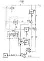
- FIG. 1 shows a station from which the data D are to be transmitted via the two-wire line L to a remote station (not shown, but constructed in the same way). Conversely, data should also be transmitted from this remote station to the station shown in FIG. 1. If data are to be transmitted simultaneously in both directions via a two-wire line, it must be known that the signal emitted by the transmitter SE must be prevented from interfering in the receiver EM of the own station. If a baseband signal is transmitted over a two-wire line, then a compensation signal is generated with the aid of a simulation stage, with the aid of which the crosstalk signal which is derived from the signals of the own transmitter SE is suppressed.
- a baseband signal is not transmitted via the two-wire line L, but instead a transmitter T is generated with the aid of the transmitter SE as a function of the data D and transmitted via the two-wire line L.
- the modulated carrier T also causes a crosstalk signal U, which is superimposed on the received signal E and which must be suppressed so as not to interfere in the receiver EM of the own station.
- the compensation signal N is generated, which is formed from the two components N1 and N2 and with the aid of which a difference signal DI is obtained using the summer SU1, which is fed to the receiver EM.
- the modulated carrier T is broken down into two orthogonal signal components K1 and K2, the phase angles of which differ by 90 °.
- one orthogonal signal component K1 is similar to the modulated carrier, whereas the other orthogonal signal component K2 is obtained with the aid of the phase rotator PH, which causes a phase rotation by 90 °.
- the component K1 represents the real part of the modulated carrier T, the component K2 the imaginary part of this modulated carrier.
- a first or second control signal R1 or R2 is generated by correlating the difference signal DI with the two orthogonal signal components K1 or K2, which signals the deviation of the one orthogonal signal component K1 from a corresponding first signal component U1 Crosstalk signal U or the deviation of the second orthogonal signal component K2 from a corresponding second signal component U2 of the crosstalk signal U is signaled.
- One simulation level NS1 or NS2 is controlled with each of the two control signals R1 and R2.
- Such simulation stages are known in connection with the transmission of baseband signals over two-wire lines.
- Known simulation stages are supplied with a baseband signal according to known methods, and a control signal is derived as a function of the crosstalk signal, and in this way interference with a transmitted baseband signal in the receiver is prevented.
- a known replication level is shown within a dashed block.
- the simulation stages NS1 and NS2 shown in FIG. 1 are in principle the same as known simulation stages.
- the signals A1 or However, A2 differ from the output signals of known simulation stages because other control signals R1 and R2 are fed to the simulation stages shown in FIG.
- the multiplicative signal N1 is obtained by multiplying the first simulation signal A1 and the signal component K1 using the multiplier MU11.
- the multiplicative signal N2 is obtained by multiplying the second simulation signal A2 and the second component K2 using the multiplier MU22. With the help of the summer SU2, the two multiplicative signals N1 and N2 are combined and the compensation signal N is obtained.
- the summer SU1 receives on the one hand the received signal E from the remote station with the superimposed crosstalk signal U and on the other hand receives the compensation signal N.
- the difference signal DI is equal to the received signal E with the crosstalk signal U minus the compensation signal N.
- the correlators KOR1 and KOR2 each consist of a multiplier MU1 and MU2 and an integrator INT1 and INT2, respectively.
- these integrators perform the task of eliminating products of orthogonal signal components when the control signals R1 and R2 are formed. At least one integration over a period is sufficient for this, since the products of these orthogonal signal components summed over a period of the orthogonal signal components are equal to zero.
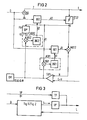
- FIG. 2 shows a station from which the data D are transmitted to a remote station, not shown. 2, as in the case of FIG. 1, receives a mixture of the received signal E and the crosstalk signal U.
- the compensation signal N is derived and the difference signal DI is derived from the Received signal E and the crosstalk signal U minus the compensation signal N are formed.
- the conditions on which FIG. 2 is based are therefore the same as the conditions described on the basis of FIG. 1.
- the modulated carrier T is first fed to the phase control stage ST22, which causes a phase shift of the modulated carrier as a function of the phase control signal A2.
- the phase signal B results at the output of the phase control stage ST22.
- Two orthogonal signal components K1 and K2 are generated from this phase signal B, the phase angles of which differ by 90 °.
- the phase signal B is the same as the signal component K1, whereas the phase signal B and the signal component K2 differ by a phase angle of 90 °.
- This phase shift is carried out with the aid of the phase shifter PH.
- the two signal components K1 and K2 are orthogonal to one another in that the products summed over a period of these signal components are zero.
- an amount control signal R1 assigned to the amount and a phase control signal R2 assigned to the phase are generated.
- the amount control signal R1 signals the deviation of one signal component K1 from the amount of the crosstalk signal U.
- the phase control signal R2 signals the deviation of the other signal component K2 from the phase angle of the crosstalk signal U.
- the magnitude control signal A1 signals the magnitude of the compensation signal N.
- the phase control signal A2 signals the phase of the compensation signal N.
- the phase of the phase signal B depends on the one hand on the phase of the modulated carrier and on the other hand on the phase control signal A2.
- the magnitude control signal A1 and the phase signal B are mixed in a multiplicative manner with the aid of the multiplier MU12, so that the compensation signal N results.
- Correlators KOR1 and KOR2 consist, as in the case of FIG. 1, of multipliers MU1 and MU2 and integrators INT1 and INT2. The statements made with regard to the integration duration in connection with FIG. 1 also apply to the integrators shown in FIG.
- FIG. 3 shows the simultaneous transmission of a voice signal and the data via a two-wire line L.
- the circuit arrangement shown in FIG. 1 or the circuit arrangement shown in FIG. 2 is to be considered.
- the data D is thus supplied to these circuit arrangements as shown in FIGS. 1 and 2.
- the high-pass HP is provided at the output of the circuit arrangement. If, in addition to the data D, the voice signal SP is also to be transmitted, then this is fed to the two-wire line L via the low-pass filter TP.
- the cut-off frequencies of the low-pass filter TP and the high-pass filter HP are defined such that two non-overlapping frequency bands are provided for the modulated carrier T on the one hand and for the speech signal SP on the other hand.
- further data D ' can optionally be transmitted in the form of a baseband data signal.
- the modulated carrier T is supplied via the high-pass HP and the further data D 'are transmitted via the low-pass TP in different frequency bands via the two-wire line L.
Claims (10)
Priority Applications (1)
| Application Number | Priority Date | Filing Date | Title |
|---|---|---|---|
| AT80102470T ATE2367T1 (de) | 1979-05-29 | 1980-05-06 | Verfahren und schaltungsanordnung zur unterdrueckung eines uebersprechsignals bei der uebertragung von daten ueber eine zweidrahtleitung. |
Applications Claiming Priority (2)
| Application Number | Priority Date | Filing Date | Title |
|---|---|---|---|
| DE2921780 | 1979-05-29 | ||
| DE2921780A DE2921780C3 (de) | 1979-05-29 | 1979-05-29 | Verfahren und Schaltungsanordnung zur Übertragung von Daten über eine Zweidrahtleitung |
Publications (2)
| Publication Number | Publication Date |
|---|---|
| EP0019755A1 EP0019755A1 (fr) | 1980-12-10 |
| EP0019755B1 true EP0019755B1 (fr) | 1983-01-26 |
Family
ID=6071947
Family Applications (1)
| Application Number | Title | Priority Date | Filing Date |
|---|---|---|---|
| EP80102470A Expired EP0019755B1 (fr) | 1979-05-29 | 1980-05-06 | Procédé et circuit pour la suppression d'un signal de diaphonic pendant la transmission de données sur deux fils |
Country Status (9)
| Country | Link |
|---|---|
| US (1) | US4370741A (fr) |
| EP (1) | EP0019755B1 (fr) |
| AT (1) | ATE2367T1 (fr) |
| AU (1) | AU532276B2 (fr) |
| BR (1) | BR8003345A (fr) |
| CA (1) | CA1140634A (fr) |
| DE (1) | DE2921780C3 (fr) |
| DK (1) | DK179680A (fr) |
| NO (1) | NO801518L (fr) |
Families Citing this family (21)
| Publication number | Priority date | Publication date | Assignee | Title |
|---|---|---|---|---|
| FR2460075B1 (fr) * | 1979-06-22 | 1988-12-09 | Cit Alcatel | Annuleur d'echo adaptatif pour transmission de donnees en duplex |
| DE3047425A1 (de) * | 1980-12-17 | 1982-07-15 | Licentia Patent-Verwaltungs-Gmbh, 6000 Frankfurt | Anordnung zur nachstellung der echoloescherkoeffizienten bei kombinierter adaptiver echoloeschung und entzerrung |
| US4464545A (en) * | 1981-07-13 | 1984-08-07 | Bell Telephone Laboratories, Incorporated | Echo canceller |
| US4669116A (en) * | 1982-12-09 | 1987-05-26 | Regents Of The University Of California | Non-linear echo cancellation of data signals |
| US4520476A (en) * | 1982-12-13 | 1985-05-28 | Rockwell International Corporation | Apparatus for enabling the duplex operation of a transmitter and receiver |
| FR2540314A1 (fr) * | 1983-01-31 | 1984-08-03 | Trt Telecom Radio Electr | Procede d'initialisation des coefficients de filtres dans un dispositif d'annulation d'echos proche et lointain et dispositif de mise en oeuvre de ce procede |
| FR2546693B1 (fr) * | 1983-05-26 | 1985-08-30 | Centre Nat Rech Scient | Annuleur d'echo a filtre numerique adaptatif pour systeme de transmission |
| US4621356A (en) * | 1983-07-18 | 1986-11-04 | Scipione Fred J | Communications interface for duplex transmission and reception of data and other signals over telephone lines |
| DE3401944A1 (de) * | 1984-01-20 | 1985-08-01 | Siemens AG, 1000 Berlin und 8000 München | 1 bit/1 bit-digitalkorrelator |
| US4715064A (en) * | 1984-06-22 | 1987-12-22 | Ncr Corporation | Adaptive hybrid circuit |
| US4682358A (en) * | 1984-12-04 | 1987-07-21 | American Telephone And Telegraph Company | Echo canceller |
| FR2614484B1 (fr) * | 1986-12-30 | 1994-04-08 | Telecommunications Sa | Terminal de transmission de donnees sur une voie analogique bidirectionnelle avec annulation d'echo couplee au rythme reception |
| US4847888A (en) * | 1988-02-16 | 1989-07-11 | Gulton Industries, Inc., Femco Division | Field telephone system |
| US4910798A (en) * | 1988-05-17 | 1990-03-20 | North American Philips Corp. | Reverse Nyquist slope filter |
| JPH09223990A (ja) * | 1996-02-19 | 1997-08-26 | Fujitsu Ltd | 伝送装置 |
| US6445698B1 (en) | 1998-09-08 | 2002-09-03 | Hyperedge Corporation | Two wire DDS transport system |
| DE19844457C1 (de) * | 1998-09-28 | 2000-07-06 | Siemens Ag | Verfahren zur Duplex-Datenübertragung mit QAM und Demodulator zur Verwendung in diesem Verfahren |
| US6901358B1 (en) * | 2001-07-03 | 2005-05-31 | Sprint Communications Company L.P. | Communication media simulation for a service provider |
| US6915250B1 (en) * | 2001-07-03 | 2005-07-05 | Sprint Communications Company L.P. | Customer premises simulation for a service provider |
| US7142501B1 (en) * | 2001-12-26 | 2006-11-28 | Cisco Technology, Inc. | Method and apparatus for eliminating near-end crosstalk in a digital subscriber line system |
| GB201408853D0 (en) * | 2014-05-19 | 2014-07-02 | Diamond Light Source Ltd | Analysis of signals from pixellated detectors of ionizing radiation |
Family Cites Families (6)
| Publication number | Priority date | Publication date | Assignee | Title |
|---|---|---|---|---|
| US1815657A (en) * | 1930-03-06 | 1931-07-21 | Int Communications Lab Inc | Submarine cable system |
| GB1434239A (en) * | 1972-08-10 | 1976-05-05 | Siemens Ag | Echo cancellers |
| US4144417A (en) * | 1975-03-07 | 1979-03-13 | Kokusai Denshin Denwa Kabushiki Kaisha | Echo cancelling system |
| DE2619712B2 (de) * | 1976-05-04 | 1978-07-13 | Siemens Ag, 1000 Berlin Und 8000 Muenchen | Schaltungsanordnung zum automatischen Abgleich eines Zweidraht-VoIlduplex-Datenübertragungssystems |
| US4074086A (en) * | 1976-09-07 | 1978-02-14 | Bell Telephone Laboratories, Incorporated | Joint adaptive echo canceller and equalizer for two-wire full-duplex data transmission |
| SE416367B (sv) * | 1976-09-07 | 1980-12-15 | Western Electric Co | Ekoelimineringsanordning |
-
1979
- 1979-05-29 DE DE2921780A patent/DE2921780C3/de not_active Expired
-
1980
- 1980-04-09 US US06/138,707 patent/US4370741A/en not_active Expired - Lifetime
- 1980-04-25 DK DK179680A patent/DK179680A/da not_active Application Discontinuation
- 1980-05-06 EP EP80102470A patent/EP0019755B1/fr not_active Expired
- 1980-05-06 AT AT80102470T patent/ATE2367T1/de not_active IP Right Cessation
- 1980-05-21 NO NO801518A patent/NO801518L/no unknown
- 1980-05-27 CA CA000352803A patent/CA1140634A/fr not_active Expired
- 1980-05-28 AU AU58829/80A patent/AU532276B2/en not_active Ceased
- 1980-05-28 BR BR8003345A patent/BR8003345A/pt unknown
Also Published As
| Publication number | Publication date |
|---|---|
| AU532276B2 (en) | 1983-09-22 |
| NO801518L (no) | 1980-12-01 |
| ATE2367T1 (de) | 1983-02-15 |
| CA1140634A (fr) | 1983-02-01 |
| DE2921780A1 (de) | 1980-12-04 |
| DE2921780C3 (de) | 1982-02-11 |
| EP0019755A1 (fr) | 1980-12-10 |
| AU5882980A (en) | 1980-12-04 |
| BR8003345A (pt) | 1980-12-30 |
| DK179680A (da) | 1980-11-30 |
| DE2921780B2 (de) | 1981-06-04 |
| US4370741A (en) | 1983-01-25 |
Similar Documents
| Publication | Publication Date | Title |
|---|---|---|
| EP0019755B1 (fr) | Procédé et circuit pour la suppression d'un signal de diaphonic pendant la transmission de données sur deux fils | |
| EP1105986A2 (fr) | Procede permettant de transmettre des informations et systeme associe | |
| DE1762361B2 (de) | Adaptiver entzerrer fuer einen digitalen datenuebertragungs kanal | |
| DE3022553A1 (de) | Echoannullierer fuer ein synchrones duplex-datenuebertragungssystem | |
| DE3025902A1 (de) | Datenuebertragungssystem nach dem streuspektrumprinzip | |
| DE3016371C2 (fr) | ||
| DE2819881C2 (de) | Vorrichtung zum Abschätzen der Fehlerrate bei Binärelementen einer numerischen Schaltung | |
| DE2800242A1 (de) | Verfahren und vorrichtung zum empfang und zur herstellung frequenzmodulierter signale | |
| DE2452997A1 (de) | Verfahren und anordnung zur funkuebertragung von binaeren informationssignalen | |
| DE1816033C3 (fr) | ||
| DE1934296A1 (de) | Vorrichtung zur UEbertragung rechteckiger synchroner Informationsimpulse | |
| DE1816033B2 (de) | Sendevorrichtung zur uebertragung von impulsen | |
| DE1088540B (de) | Verfahren und Vorrichtung zur UEbertragung von Informationen | |
| DE2033017A1 (de) | Vorrichtung zum Empfang mehrerer Eingangssignale gleicher Frequenz | |
| DE2257288C3 (fr) | ||
| DE2516099A1 (de) | Schaltungsanordnung zur automatischen entzerrung | |
| DE2221524B2 (de) | Schaltungsanordnung zum empfangsseitigen Erweitern des Störabstandes in Nachrichten-Übertragungsanlagen | |
| DE2208293A1 (de) | Simulator | |
| DE631106C (de) | Fremdgesteuertes Gleichwellensendesystem | |
| DE935613C (de) | Verfahren zur Nachrichtenuebertragung mittels Pulszeitmodulation | |
| DE1160038B (de) | Verfahren und Vorrichtung zur UEbertragung von zwei oder mehreren Signalen | |
| DE3031190A1 (de) | Verfahren und schaltungsanordnung zur einstellbaren frequenzmaessigen begrenzung eines signals | |
| DE3245244C1 (de) | Methode zur simultanen Übertragung von binären Daten und Telefonsprechsignalen innerhalb des Sprachbandes eines Telefon-Übertragungskanals | |
| DE1157677B (de) | Entzerrerschaltung fuer ein Mehrkanalsystem zur UEbertragung von amplitudenmodulierten Impulsen | |
| DE2223842C3 (de) | Anordnung zur Übertragung eines Signals |
Legal Events
| Date | Code | Title | Description |
|---|---|---|---|
| PUAI | Public reference made under article 153(3) epc to a published international application that has entered the european phase |
Free format text: ORIGINAL CODE: 0009012 |
|
| AK | Designated contracting states |
Designated state(s): AT BE CH FR GB IT NL SE |
|
| 17P | Request for examination filed |
Effective date: 19810109 |
|
| ITF | It: translation for a ep patent filed |
Owner name: STUDIO JAUMANN |
|
| GRAA | (expected) grant |
Free format text: ORIGINAL CODE: 0009210 |
|
| AK | Designated contracting states |
Designated state(s): AT BE CH FR GB IT LI NL SE |
|
| REF | Corresponds to: |
Ref document number: 2367 Country of ref document: AT Date of ref document: 19830215 Kind code of ref document: T |
|
| ET | Fr: translation filed | ||
| PGFP | Annual fee paid to national office [announced via postgrant information from national office to epo] |
Ref country code: FR Payment date: 19840524 Year of fee payment: 5 |
|
| PGFP | Annual fee paid to national office [announced via postgrant information from national office to epo] |
Ref country code: SE Payment date: 19840630 Year of fee payment: 5 Ref country code: BE Payment date: 19840630 Year of fee payment: 5 |
|
| PGFP | Annual fee paid to national office [announced via postgrant information from national office to epo] |
Ref country code: CH Payment date: 19840824 Year of fee payment: 5 |
|
| PGFP | Annual fee paid to national office [announced via postgrant information from national office to epo] |
Ref country code: AT Payment date: 19860430 Year of fee payment: 7 |
|
| PG25 | Lapsed in a contracting state [announced via postgrant information from national office to epo] |
Ref country code: SE Effective date: 19860507 |
|
| PG25 | Lapsed in a contracting state [announced via postgrant information from national office to epo] |
Ref country code: BE Effective date: 19860531 |
|
| PGFP | Annual fee paid to national office [announced via postgrant information from national office to epo] |
Ref country code: NL Payment date: 19860531 Year of fee payment: 7 |
|
| BERE | Be: lapsed |
Owner name: SIEMENS A.G. BERLIN UND MUNCHEN Effective date: 19860531 |
|
| GBPC | Gb: european patent ceased through non-payment of renewal fee | ||
| PG25 | Lapsed in a contracting state [announced via postgrant information from national office to epo] |
Ref country code: FR Free format text: LAPSE BECAUSE OF NON-PAYMENT OF DUE FEES Effective date: 19870130 |
|
| REG | Reference to a national code |
Ref country code: FR Ref legal event code: ST |
|
| PG25 | Lapsed in a contracting state [announced via postgrant information from national office to epo] |
Ref country code: AT Effective date: 19870506 |
|
| PG25 | Lapsed in a contracting state [announced via postgrant information from national office to epo] |
Ref country code: LI Effective date: 19870531 Ref country code: CH Effective date: 19870531 |
|
| PG25 | Lapsed in a contracting state [announced via postgrant information from national office to epo] |
Ref country code: NL Effective date: 19871201 |
|
| NLV4 | Nl: lapsed or anulled due to non-payment of the annual fee | ||
| REG | Reference to a national code |
Ref country code: CH Ref legal event code: PL |
|
| PG25 | Lapsed in a contracting state [announced via postgrant information from national office to epo] |
Ref country code: GB Effective date: 19881118 |
|
| ITTA | It: last paid annual fee | ||
| EUG | Se: european patent has lapsed |
Ref document number: 80102470.4 Effective date: 19870225 |
|
| PLBE | No opposition filed within time limit |
Free format text: ORIGINAL CODE: 0009261 |
|
| STAA | Information on the status of an ep patent application or granted ep patent |
Free format text: STATUS: NO OPPOSITION FILED WITHIN TIME LIMIT |