EP0010952B1 - Verfahren und Vorrichtung zur Beheizung von Halbleiterscheiben - Google Patents
Verfahren und Vorrichtung zur Beheizung von Halbleiterscheiben Download PDFInfo
- Publication number
- EP0010952B1 EP0010952B1 EP79302378A EP79302378A EP0010952B1 EP 0010952 B1 EP0010952 B1 EP 0010952B1 EP 79302378 A EP79302378 A EP 79302378A EP 79302378 A EP79302378 A EP 79302378A EP 0010952 B1 EP0010952 B1 EP 0010952B1
- Authority
- EP
- European Patent Office
- Prior art keywords
- wafers
- heating
- tube
- length
- reaction zone
- Prior art date
- Legal status (The legal status is an assumption and is not a legal conclusion. Google has not performed a legal analysis and makes no representation as to the accuracy of the status listed.)
- Expired
Links
Images
Classifications
-
- C—CHEMISTRY; METALLURGY
- C30—CRYSTAL GROWTH
- C30B—SINGLE-CRYSTAL GROWTH; UNIDIRECTIONAL SOLIDIFICATION OF EUTECTIC MATERIAL OR UNIDIRECTIONAL DEMIXING OF EUTECTOID MATERIAL; REFINING BY ZONE-MELTING OF MATERIAL; PRODUCTION OF A HOMOGENEOUS POLYCRYSTALLINE MATERIAL WITH DEFINED STRUCTURE; SINGLE CRYSTALS OR HOMOGENEOUS POLYCRYSTALLINE MATERIAL WITH DEFINED STRUCTURE; AFTER-TREATMENT OF SINGLE CRYSTALS OR A HOMOGENEOUS POLYCRYSTALLINE MATERIAL WITH DEFINED STRUCTURE; APPARATUS THEREFOR
- C30B33/00—After-treatment of single crystals or homogeneous polycrystalline material with defined structure
-
- C—CHEMISTRY; METALLURGY
- C30—CRYSTAL GROWTH
- C30B—SINGLE-CRYSTAL GROWTH; UNIDIRECTIONAL SOLIDIFICATION OF EUTECTIC MATERIAL OR UNIDIRECTIONAL DEMIXING OF EUTECTOID MATERIAL; REFINING BY ZONE-MELTING OF MATERIAL; PRODUCTION OF A HOMOGENEOUS POLYCRYSTALLINE MATERIAL WITH DEFINED STRUCTURE; SINGLE CRYSTALS OR HOMOGENEOUS POLYCRYSTALLINE MATERIAL WITH DEFINED STRUCTURE; AFTER-TREATMENT OF SINGLE CRYSTALS OR A HOMOGENEOUS POLYCRYSTALLINE MATERIAL WITH DEFINED STRUCTURE; APPARATUS THEREFOR
- C30B25/00—Single-crystal growth by chemical reaction of reactive gases, e.g. chemical vapour-deposition growth
- C30B25/02—Epitaxial-layer growth
- C30B25/10—Heating of the reaction chamber or the substrate
-
- C—CHEMISTRY; METALLURGY
- C30—CRYSTAL GROWTH
- C30B—SINGLE-CRYSTAL GROWTH; UNIDIRECTIONAL SOLIDIFICATION OF EUTECTIC MATERIAL OR UNIDIRECTIONAL DEMIXING OF EUTECTOID MATERIAL; REFINING BY ZONE-MELTING OF MATERIAL; PRODUCTION OF A HOMOGENEOUS POLYCRYSTALLINE MATERIAL WITH DEFINED STRUCTURE; SINGLE CRYSTALS OR HOMOGENEOUS POLYCRYSTALLINE MATERIAL WITH DEFINED STRUCTURE; AFTER-TREATMENT OF SINGLE CRYSTALS OR A HOMOGENEOUS POLYCRYSTALLINE MATERIAL WITH DEFINED STRUCTURE; APPARATUS THEREFOR
- C30B31/00—Diffusion or doping processes for single crystals or homogeneous polycrystalline material with defined structure; Apparatus therefor
- C30B31/06—Diffusion or doping processes for single crystals or homogeneous polycrystalline material with defined structure; Apparatus therefor by contacting with diffusion material in the gaseous state
- C30B31/12—Heating of the reaction chamber
Definitions
- the present invention relates to a method for heating semiconductor wafers and to an apparatus for carrying out such a method.
- Processes for manufacturing semiconductor devices involve steps in which an impurity is caused to diffuse into a wafer, or a coating is formed on at least one surface of a wafer.
- a diffusion of an impurity or a formation of a coating is effected by heating a wafer in an atmosphere within a reaction tube, which is heated by a furnace surrounding the tube. More specifically, an elongated reaction tube is horizontally placed in a furnace surrounding the effective length of the reaction tube, and heated to a predetermined temperature.
- An appropriate gas such as N 2 , 0 2 or H 2 , is allowed to pass through the reaction tube to establish a desired atmosphere.
- Arrays of wafers supported by a holder are then introduced into the reaction tube from one end thereof, allowed to stay there for a predetermined period of time, and then withdrawn from the same end of the tube.
- refractory metal materials can not be used for the construction of such mechanical means, because the intended doping is adversely affected due to impurities from such metallic materials.
- materials such as, quartz, SiC, polycrystalline silicon or SiN 4 , will be required. Due to significant thermal distortion at high temperatures and poor fabrication precision of such materials, smooth movement of wafers through the high temperature zone is not ensured.
- the wafers and holders are always moving together with the mechanical means, formation of dust is unavoidable, leading to a reduction in the yield (the production of faulty products).
- This method and apparatus is an improvement over known methods in which the wafers are moved up and down the reaction zone, but it is limited to the high frequency induction heating of small numbers of separate wafers on susceptor blocks.
- the method is not suitable for heating large numbers of wafers.
- a method for heating semiconductor wafers wherein the semiconductor wafers are heated in an atmosphere within an elongate reaction zone by a heating means surrounding the reaction zone and short in relation to the length of the reaction zone, and in which in each wafer-heating operation, the heating means is caused to move continuously so that it will passs over each wafer placed in the reaction zone, is characterized in that the heating means exhibits a temperature profile, in the direction of the length of the reaction zone, which rises progressively to a peak and then falls progressively, with no flat portion along its length and in that the wafers are stacked with their main surfaces perpendicular to the length of the reaction zone.
- the length of the heating means is therefore such that it surrounds only a part of the length of the reaction zone at any time, and preferably the heating means is moved at a constant speed along the reaction zone. If desired, the heating means may be passed once in each direction for each charge of wafers to be heated. Preferably the reaction zone is preheated to a temperature which is less than the temperature at which the intended reaction is to take place.
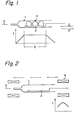
- an elongated reaction tube 1 is horizontally placed in a fixed electric furnace (not shown) surrounding the tube and heated to a predetermined temperature.
- the furnace is such that it provides a heating zone exhibiting a temperature profile having a flat portion D, as shown in Fig. 1.
- a gas 5 to establish a desired atmosphere is then allowed to pass through the reaction tube 1.
- a wafer holder 2 carrying three arrays of wafers 3 is then introduced into the reaction tube 1 from a direction indicated by an arrow Q. All the wafers should be placed in those areas of the reaction tube 1 which correspond to the flat portion D of the temperature profile of the furnace.
- the wafer holder 2 carrying the arrays of wafers 3 is withdrawn from the heated reaction tube in a direction indicated by an arrow Q'.
- this heating procedure it will be understood that wafers in the left end array receive more heat than those in the right end array.
- the integrated heat quantity is different from portion to portion in a single wafer. Uneven heating of wafers results in variations in the sheet resistivity, thickness of oxide coating, current amplification factor, cut off frequency and/or other properties of the semiconductor device products.
- a gas 5 is allowed to pass through a horizontal elongated reaction tube 1.
- the tube 1 may be at ambient temperature, or may be preheated to a temperature of several hundred degrees C, at which the intended reaction does not take place.
- a wafer holder 2 carrying wafers is then introduced into the center of the reaction tube 1 from one end of the tube 1.
- a movable electric furnace 4 surrounding a part of the whole length of the reaction tube which is movable along the reaction tube 1 and is initially placed at that end of the tube 1 from which the wafers have been introduced into the tube 1, is then caused to start to move in the direction designated by arrows in Fig. 2, so that it will pass over each wafer placed in the tube 1 and reach the other end of the tube 1.
- the wafers can be evenly heated.
- an electric furnace is preferred, other furnaces such as an infra red furnace can also be used in the practice of the invention.
- a heating zone formed by the furnace 4, when it is stationary, is such that it exhibits a temperature distribution or profile along the length, as shown in Fig.
- the furnace having a distinct peak at the center in the temperature profile, and we prefer the furnace to move at a constant speed.
- the properties of the products including, for example, the depth of diffusion, sheet resistivity, and thickness of oxide coating, may be controlled by appropriately selecting the peak temperature of the furnace and the moving speed of the furnace. In most cases, we select the peak temperature of the furnace within the range between 1,000°C and 1,250°C, and the moving speed of the furnace within the range between 10 cm/min and 100 cm/min.
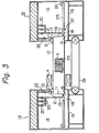
- the apparatus for heating wafers shown in Fig. 3, in accordance with one embodiment of the invention, comprises a horizontal elongate cylindrical reaction tube 10.
- the tube 10 is made of quartz glass and has caps 11 of quartz glass detachably mounted at both ends thereof.
- the cap 11 is attachable to one end of the tube 10, by a ground glass fitting 12 forming a gas tight connection.
- the tube 10 opens at that end to a space 13 within a clean bench generally designated by the numeral 14.
- the cap 11 is provided with a gas inlet pipe 16 and a gas outlet pipe 17.
- the inlet pipe 16 is connected to a pipe 19 by a joint 18, and the pipe 19 is branched into three pipes, each communicating, via a valve 20, with a different gas source (not shown).
- the outlet pipe 17 communicates with a gas exhaust system (not shown) via a joint 21 and valve 22.
- Such a means may comprise a hollow rotating shaft 25 driven by a motor 26 at one end of the shaft via a worm gear (not shown), a threaded nut 27 axially mounted to the shaft 25 at the other end of the shaft, and a screw rod (not shown) engaged with the nut 27.
- the rotation of the shaft 25 may be converted to the linear movement of the screw rod, which may be transmitted to a quartz rod (not shown) attached to the screw rod in parallel so as to push or pull the boat 23.
- the apparatus is further provided with an electric furnace 4 surrounding a part of the length of the reaction tube 10 for heating that part of the tube surrounded by the furnace. Endless chains 29 driven by a motor (not shown) may drive the furnace 4 along the reaction tube 10. When the furnace 4 is stationary it forms a heating zone exhibiting a temperature distribution with no flat portions along the length of the furnace, as shown in Fig. 2.
- the furnace 4 which is placed at one end (the left end, in the illustrated case) of the reaction tube, is caused to start to heat.
- the cap 11 is detached from the reaction tube 11 by disconnecting the joints 18 and 21.
- the wafer boat 23 is withdrawn from the tube 10 and, then, loaded with wafers 3 to be processed.
- the boat 23 is then placed in the center of the tube 10, and the cap 11 is attached to the tube in the right clean bench.
- a required gas is sent through the tube, from the left to the right in the illustrated case, by appropriately adjusting the valves 20 and 22.
- the furnace 4 is then caused to move at a predetermined speed along the reaction tube 10 until it reaches the right end of the tube.
- the cap 11 in the left clean bench is then removed from the tube, and the boat 23 is withdrawn from the tube to the left clean bench in order to remove the treated wafers.
- fresh wafers may be charged from the left clean bench and the treated wafers may be removed at the right clean bench.
- the furnace 4 is caused to travel along the tube 10 from right to left under a gas flow from right to left.
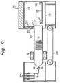
- Fig. 4 illustrates an apparatus in accordance with another embodiment of the invention.
- the apparatus comprises a reaction tube 10' having a cap 11' detachably mounted to one end thereof.
- the cap 11' has only a gas outlet pipe 17 communicated with the gas exhaust system in the same manner as hereinabove described with reference to Fig. 3.
- the reaction tube 10' has a gas inlet pipe 16 at the other end thereof, which inlet pipe 16 is communicated with the gas supply system in the manner as described with reference to Fig. 3.
- the same numerals designate the same parts.
- the furnace 4 is caused to travel along the tube from left to right and then from right to left for the processing of one lot of wafers.
- the wafers so processed are then withdrawn from the reaction tube to the clean bench 14.
- the furnace 4 can be as short as about 50 cm in length for the reaction tube 10 of a length of about 2 to 3 m.
- the method and apparatus according to the invention are generally useful for evenly heating semiconductor wafers, they are particularly suitable for use in the treatment of wafers at a high temperature for a short period of time, as is the case with an anneal after ion implantation and a solid-to-solid diffusion.
- a junction depth of the order of 3000 A and a sheet resistivity of 950 Q/square can be achieved by a conventional method using the annealing conditions of 1000°C, 30 minutes, in N 2 .
- the same order of the junction depth and a sheet resistivity of 900 ⁇ /square can be achieved using a peak temperature of 1 180°C and a moving speed of 30 cm/min. This reveals that better activation of implanted atoms is achievable in accordance with the invention than with the conventional method.
- a wafer 10 cms in diameter tends to crack if it is repeatedly subjected to such a quick diffusion processing 3 to 4 times. This is not the case if such a wafer is treated in accordance with the invention.
- the same orders of the current amplification factor and the cut off frequency can be achieved either by a quick diffusion technique with a furnace temperature of 1150°C, a boat loader speed of 300 cm/min and a diffusion time of 90 seconds, or by a method of the invention with a peak temperature of 1180°C and a moving speed of the furnace of 25 cm/min.
- the total processing time required for the treatment of 50 wafers is about 90 min for the quick diffusion technique and about 10 min for the method of the invention.
Landscapes
- Chemical & Material Sciences (AREA)
- Engineering & Computer Science (AREA)
- Crystallography & Structural Chemistry (AREA)
- Materials Engineering (AREA)
- Metallurgy (AREA)
- Organic Chemistry (AREA)
- Chemical Kinetics & Catalysis (AREA)
- General Chemical & Material Sciences (AREA)
Claims (5)
Applications Claiming Priority (2)
| Application Number | Priority Date | Filing Date | Title |
|---|---|---|---|
| JP134140/78 | 1978-10-31 | ||
| JP53134140A JPS584811B2 (ja) | 1978-10-31 | 1978-10-31 | 半導体装置の製造方法 |
Publications (2)
| Publication Number | Publication Date |
|---|---|
| EP0010952A1 EP0010952A1 (de) | 1980-05-14 |
| EP0010952B1 true EP0010952B1 (de) | 1983-06-08 |
Family
ID=15121400
Family Applications (1)
| Application Number | Title | Priority Date | Filing Date |
|---|---|---|---|
| EP79302378A Expired EP0010952B1 (de) | 1978-10-31 | 1979-10-30 | Verfahren und Vorrichtung zur Beheizung von Halbleiterscheiben |
Country Status (4)
| Country | Link |
|---|---|
| US (1) | US4449037A (de) |
| EP (1) | EP0010952B1 (de) |
| JP (1) | JPS584811B2 (de) |
| DE (1) | DE2965631D1 (de) |
Families Citing this family (17)
| Publication number | Priority date | Publication date | Assignee | Title |
|---|---|---|---|---|
| JPS59193024A (ja) * | 1983-03-29 | 1984-11-01 | Ushio Inc | 閃光照射装置 |
| US4573431A (en) * | 1983-11-16 | 1986-03-04 | Btu Engineering Corporation | Modular V-CVD diffusion furnace |
| US4794217A (en) * | 1985-04-01 | 1988-12-27 | Qing Hua University | Induction system for rapid heat treatment of semiconductor wafers |
| JPS6255453U (de) * | 1985-09-26 | 1987-04-06 | ||
| KR880701060A (ko) * | 1985-11-12 | 1988-04-22 | 원본미기재 | 유도 가열된 물질의 냉각 장치 및 방법 |
| JPS62166624U (de) * | 1986-04-14 | 1987-10-22 | ||
| US4721836A (en) * | 1986-05-14 | 1988-01-26 | The United States Of America As Represented By The Secretary Of The Navy | Apparatus for transient annealing of semiconductor samples in a controlled ambient |
| JPS62271420A (ja) * | 1987-01-16 | 1987-11-25 | Sony Corp | 半導体基体の処理装置 |
| KR880010481A (ko) * | 1987-02-21 | 1988-10-10 | 강진구 | 액상 박막 결정 성장방법 및 장치 |
| US5093557A (en) * | 1989-05-16 | 1992-03-03 | Microscience, Inc. | Substrate heater and heating element |
| US4982347A (en) * | 1989-06-22 | 1991-01-01 | Unisys Corporation | Process and apparatus for producing temperature profiles in a workpiece as it passes through a belt furnace |
| US5064367A (en) * | 1989-06-28 | 1991-11-12 | Digital Equipment Corporation | Conical gas inlet for thermal processing furnace |
| JPH04297025A (ja) * | 1991-01-10 | 1992-10-21 | Nec Corp | 半導体製造装置 |
| JP4906018B2 (ja) * | 2001-03-12 | 2012-03-28 | 株式会社半導体エネルギー研究所 | 成膜方法、発光装置の作製方法及び成膜装置 |
| US7037376B2 (en) * | 2003-04-11 | 2006-05-02 | Applied Materials Inc. | Backflush chamber clean |
| TWI545298B (zh) * | 2010-06-04 | 2016-08-11 | 信越化學工業股份有限公司 | Heat treatment furnace |
| EP4143363A1 (de) * | 2020-06-08 | 2023-03-08 | Okinawa Institute of Science and Technology School Corporation | Schnelle hybride chemische gasphasenabscheidung für perowskit-solarmodule |
Family Cites Families (12)
| Publication number | Priority date | Publication date | Assignee | Title |
|---|---|---|---|---|
| US3031338A (en) * | 1959-04-03 | 1962-04-24 | Alloyd Res Corp | Metal deposition process and apparatus |
| US3524776A (en) * | 1967-01-30 | 1970-08-18 | Corning Glass Works | Process for coating silicon wafers |
| US3657006A (en) * | 1969-11-06 | 1972-04-18 | Peter D Fisher | Method and apparatus for depositing doped and undoped glassy chalcogenide films at substantially atmospheric pressure |
| US3828722A (en) * | 1970-05-01 | 1974-08-13 | Cogar Corp | Apparatus for producing ion-free insulating layers |
| JPS4834798A (de) * | 1971-09-06 | 1973-05-22 | ||
| FR2178751B1 (de) * | 1972-04-05 | 1974-10-18 | Radiotechnique Compelec | |
| US4129090A (en) * | 1973-02-28 | 1978-12-12 | Hitachi, Ltd. | Apparatus for diffusion into semiconductor wafers |
| JPS49126260A (de) * | 1973-04-04 | 1974-12-03 | ||
| US3900597A (en) * | 1973-12-19 | 1975-08-19 | Motorola Inc | System and process for deposition of polycrystalline silicon with silane in vacuum |
| JPS5936417B2 (ja) * | 1975-11-26 | 1984-09-04 | 株式会社デンソー | 半導体基板への高周波誘導加熱による拡散装置 |
| US4033286A (en) * | 1976-07-12 | 1977-07-05 | California Institute Of Technology | Chemical vapor deposition reactor |
| US4275094A (en) * | 1977-10-31 | 1981-06-23 | Fujitsu Limited | Process for high pressure oxidation of silicon |
-
1978
- 1978-10-31 JP JP53134140A patent/JPS584811B2/ja not_active Expired
-
1979
- 1979-10-30 DE DE7979302378T patent/DE2965631D1/de not_active Expired
- 1979-10-30 EP EP79302378A patent/EP0010952B1/de not_active Expired
-
1982
- 1982-05-14 US US06/378,261 patent/US4449037A/en not_active Expired - Lifetime
Also Published As
| Publication number | Publication date |
|---|---|
| JPS5561021A (en) | 1980-05-08 |
| JPS584811B2 (ja) | 1983-01-27 |
| EP0010952A1 (de) | 1980-05-14 |
| US4449037A (en) | 1984-05-15 |
| DE2965631D1 (en) | 1983-07-14 |
Similar Documents
| Publication | Publication Date | Title |
|---|---|---|
| EP0010952B1 (de) | Verfahren und Vorrichtung zur Beheizung von Halbleiterscheiben | |
| US4760244A (en) | Apparatus for the treatment of semiconductor materials | |
| US4640223A (en) | Chemical vapor deposition reactor | |
| JP3190165B2 (ja) | 縦型熱処理装置及び熱処理方法 | |
| JPH1064836A (ja) | 縦型熱処理炉 | |
| EP1182692A2 (de) | Wärmebehandlungsgerät und Verfahren zum Behandeln von Halbleitern | |
| JPS6411712B2 (de) | ||
| KR100217542B1 (ko) | 열 처리 방법 | |
| JPS5861635A (ja) | 半導体の処理方法 | |
| US9799535B2 (en) | Heat-treatment furnace | |
| JP2668001B2 (ja) | 熱処理方法及びその装置 | |
| US4147432A (en) | Apparatus for thermal diffusion by high frequency induction heating of semiconductor substrates | |
| KR900000835B1 (ko) | 서스펜션 캔릴레버(Suspension Cantilever) 로딩장치(Loading system)를 갖는 횡형로(橫型爐) | |
| JP2002299319A (ja) | 基板処理装置 | |
| EP1454367A2 (de) | Backofen für photovoltaische vorrichtungen | |
| US4556437A (en) | Method of diffusing silicon slices with doping materials | |
| JPS63232422A (ja) | 半導体ウエハの熱処理装置 | |
| JP3497317B2 (ja) | 半導体熱処理方法およびそれに用いる装置 | |
| JP3534518B2 (ja) | 半導体熱処理方法およびそれに用いる装置 | |
| JP2008283143A (ja) | 処理装置、トランジスタ製造方法 | |
| JPH0534821B2 (de) | ||
| WO2017018366A1 (ja) | 多結晶シリコン製造用反応炉及び多結晶シリコンの製造方法 | |
| GB2164796A (en) | Semiconductor processing | |
| US3467557A (en) | Polycrystalline semiconductor devices | |
| JPH08330245A (ja) | 半導体装置の製造方法及び半導体装置の製造装置 |
Legal Events
| Date | Code | Title | Description |
|---|---|---|---|
| PUAI | Public reference made under article 153(3) epc to a published international application that has entered the european phase |
Free format text: ORIGINAL CODE: 0009012 |
|
| 17P | Request for examination filed | ||
| AK | Designated contracting states |
Designated state(s): DE FR GB NL |
|
| GRAA | (expected) grant |
Free format text: ORIGINAL CODE: 0009210 |
|
| AK | Designated contracting states |
Designated state(s): DE FR GB NL |
|
| REF | Corresponds to: |
Ref document number: 2965631 Country of ref document: DE Date of ref document: 19830714 |
|
| ET | Fr: translation filed | ||
| PLBE | No opposition filed within time limit |
Free format text: ORIGINAL CODE: 0009261 |
|
| STAA | Information on the status of an ep patent application or granted ep patent |
Free format text: STATUS: NO OPPOSITION FILED WITHIN TIME LIMIT |
|
| 26N | No opposition filed | ||
| PGFP | Annual fee paid to national office [announced via postgrant information from national office to epo] |
Ref country code: NL Payment date: 19921031 Year of fee payment: 14 |
|
| PG25 | Lapsed in a contracting state [announced via postgrant information from national office to epo] |
Ref country code: NL Effective date: 19940501 |
|
| NLV4 | Nl: lapsed or anulled due to non-payment of the annual fee | ||
| PGFP | Annual fee paid to national office [announced via postgrant information from national office to epo] |
Ref country code: FR Payment date: 19971009 Year of fee payment: 19 |
|
| PGFP | Annual fee paid to national office [announced via postgrant information from national office to epo] |
Ref country code: GB Payment date: 19971021 Year of fee payment: 19 |
|
| PGFP | Annual fee paid to national office [announced via postgrant information from national office to epo] |
Ref country code: DE Payment date: 19971110 Year of fee payment: 19 |
|
| PG25 | Lapsed in a contracting state [announced via postgrant information from national office to epo] |
Ref country code: GB Free format text: LAPSE BECAUSE OF NON-PAYMENT OF DUE FEES Effective date: 19981030 |
|
| GBPC | Gb: european patent ceased through non-payment of renewal fee |
Effective date: 19981030 |
|
| PG25 | Lapsed in a contracting state [announced via postgrant information from national office to epo] |
Ref country code: FR Free format text: LAPSE BECAUSE OF NON-PAYMENT OF DUE FEES Effective date: 19990630 |
|
| REG | Reference to a national code |
Ref country code: FR Ref legal event code: ST |
|
| PG25 | Lapsed in a contracting state [announced via postgrant information from national office to epo] |
Ref country code: DE Free format text: LAPSE BECAUSE OF NON-PAYMENT OF DUE FEES Effective date: 19990803 |