EP0003609B1 - Hochspannungsfester Optokoppler - Google Patents
Hochspannungsfester Optokoppler Download PDFInfo
- Publication number
- EP0003609B1 EP0003609B1 EP79100412A EP79100412A EP0003609B1 EP 0003609 B1 EP0003609 B1 EP 0003609B1 EP 79100412 A EP79100412 A EP 79100412A EP 79100412 A EP79100412 A EP 79100412A EP 0003609 B1 EP0003609 B1 EP 0003609B1
- Authority
- EP
- European Patent Office
- Prior art keywords
- radiation
- optocoupler
- insulating film
- mass
- coupling medium
- Prior art date
- Legal status (The legal status is an assumption and is not a legal conclusion. Google has not performed a legal analysis and makes no representation as to the accuracy of the status listed.)
- Expired
Links
- 230000005855 radiation Effects 0.000 claims description 27
- 230000008878 coupling Effects 0.000 claims description 19
- 238000010168 coupling process Methods 0.000 claims description 19
- 238000005859 coupling reaction Methods 0.000 claims description 19
- 239000004020 conductor Substances 0.000 claims description 11
- 230000015556 catabolic process Effects 0.000 claims description 7
- 239000000463 material Substances 0.000 claims description 7
- 229920001296 polysiloxane Polymers 0.000 claims description 7
- 229920005989 resin Polymers 0.000 claims description 2
- 239000011347 resin Substances 0.000 claims description 2
- 239000002966 varnish Substances 0.000 claims 2
- 150000002118 epoxides Chemical class 0.000 claims 1
- 239000003822 epoxy resin Substances 0.000 claims 1
- 229920000647 polyepoxide Polymers 0.000 claims 1
- 150000001875 compounds Chemical class 0.000 description 13
- 238000005538 encapsulation Methods 0.000 description 10
- 239000004922 lacquer Substances 0.000 description 4
- 238000004519 manufacturing process Methods 0.000 description 4
- 239000011248 coating agent Substances 0.000 description 2
- 238000000576 coating method Methods 0.000 description 2
- 238000000465 moulding Methods 0.000 description 2
- 239000004593 Epoxy Substances 0.000 description 1
- 238000005266 casting Methods 0.000 description 1
- 239000008199 coating composition Substances 0.000 description 1
- 229920006336 epoxy molding compound Polymers 0.000 description 1
- 239000011521 glass Substances 0.000 description 1
Images
Classifications
-
- H—ELECTRICITY
- H10—SEMICONDUCTOR DEVICES; ELECTRIC SOLID-STATE DEVICES NOT OTHERWISE PROVIDED FOR
- H10F—INORGANIC SEMICONDUCTOR DEVICES SENSITIVE TO INFRARED RADIATION, LIGHT, ELECTROMAGNETIC RADIATION OF SHORTER WAVELENGTH OR CORPUSCULAR RADIATION
- H10F55/00—Radiation-sensitive semiconductor devices covered by groups H10F10/00, H10F19/00 or H10F30/00 being structurally associated with electric light sources and electrically or optically coupled thereto
- H10F55/20—Radiation-sensitive semiconductor devices covered by groups H10F10/00, H10F19/00 or H10F30/00 being structurally associated with electric light sources and electrically or optically coupled thereto wherein the electric light source controls the radiation-sensitive semiconductor devices, e.g. optocouplers
Definitions
- the invention relates to a high-voltage-resistant optocoupler, each with a radiation transmitter or radiation receiver arranged on a conductor strip, between which a radiation-permeable coupling medium is provided which is at least partially enveloped by a radiation-impermeable mass.
- At least one conductor strip including the radiation transmitter or receiver is covered with a radiation-permeable insulating film in order to prevent voltage breakdowns at the interface between the coupling medium and the encapsulation compound.
- the insulating film which may consist of silicone lacquer or epoxy lacquer, for example, is applied to the conductor strip after the radiation transmitter or radiation receiver has been applied, thus preventing breakdown at the interface between the coupling medium and the encapsulation compound. This can increase the dielectric strength of the optocoupler by up to 10 kV.
- a radiation-permeable insulating film it is possible to coat the radiation transmitter or receiver without the need for an exclusive removal of the film in the area of these components.
- the coating composition is a silicone molding compound or an epoxy molding compound or casting resin.
- a further development of the invention consists in the fact that the insulating film on the delivery tapes extends into the vicinity of the exit of the conductor tapes from the encapsulation compound. This ensures that no electrical breakdown can occur around the insulating film to the interface between the coupling medium and the encapsulation compound.
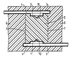
- a radiation transmitter 1 or radiation receiver 2 are applied to conductor strips 4.
- the radiation transmitter 1 can be a light-emitting diode, while a photodiode or a phototransistor can be provided for the radiation receiver 2.
- a coupling medium 3 made of, for example, silicone lacquer is located between the radiation transmitter 1 and the radiation receiver 2.
- the coupling medium 3 is encased by a coating compound 6 made of silicone molding compound which, in contrast to the coupling medium 3, is opaque.
- the connecting wires 10 of the radiation transmitter 1 or of the radiation receiver 2 are only shown schematically and each lead to the conductor strips 4.
- an electrical breakdown can preferably occur at the interface 7 between the coupling medium 3 and the enveloping mass 6.
Landscapes
- Photo Coupler, Interrupter, Optical-To-Optical Conversion Devices (AREA)
Description
- Die Erfindung betrifft einen hochspannungsfesten Optokoppler, mit einem jeweils auf einem Leiterband angeordneten Strahlungssender beziehungsweise Strahlungsemgfänger, zwischen denen ein strahlungsdurchlässiges Koppelmedium vorgesehen ist, das wenigstens teilweise von einer strahlungsundurchlässigen Masse umhüllt ist.
- Es gibt bereits einen Optokoppler (DE-OS 27 03 456), bei dem zwischen dem Strahlungssender und dem Strahlungsempfänger eine Glasschicht hoher Durchschlagsfestigkeit angeordnet ist, um so den Optokoppler bei höheren Spannungen betreiben zu können.
- Wenn bei einem Optokoppler das Koppelmedium und die dieses umhüllende Masse aus verschiedenen Werkstoffen bestehen, so hat sich gezeigt, daß ein elektrischer Durchschlag in erster Linie an der Grenzfläche zwischen dem Koppelmedium und der Umhüllungsmasse auftritt. Daher werden oft Optokoppler hergestellt, bei denen das Koppelmedium und die Umhüllungsmasse aus dem gleichen Werkstoff bestehen. Trotzdem werden aber für viele Anwendungsfälle Optokoppler mit unterschiedlichen Werkstoffen für das Koppelmedium und die Umhüllungsmasse bevorzugt, so daß in der Fertigung derzeit zwei Fertigungsstraßen eingesetzt werden, nämlich eine Fertigungsstraße für hochspannungsfeste Optokoppler mit einem Werkstoff für Koppelmedium und Umfiullungsmasse und eine weitere Fertigungsstraße für Optokoppler mit verschiedenen Werkstoffen für Koppelmedium und Umhüllungsmasse.
- Es ist nun Aufgabe der Erfindung, einen Optokoppler mit verschiedenen Werkstoffen für Koppelmedium un Umhüllungsmasse auzugeben, der aber dennoch ausreichend hochspannungsfest gegenüber Spannungsdurchschlägen au der Grenzfläche zwischen Koppelmedium un Umhüllungsmasse ist.
- Diese Aufgabe wird erfindungsgemäß dadurch gelöst, dass wenigstens ein Leiterband samt Strahlungssender bzw. -empfänger mit einem strahlungsdurchlässigen Isolierfilm überzogen ist, um Spannungsdurchschläge an der Grenzfläche zwischen Koppelmedium und Umhüllungsmasse zu verhindern.
- Der Isolierfilm, der zum Beispiel aus Siliconlack oder Epoxydlack bestehen kann, wird nach dem Aufbringen des Strahlungssenders beziehungsweise Strahlungsempfängers auf das Leiterband aufgetragen und verhindert so einen Durchschlag an der Grenzfläche zwischen dem Koppelmedium und der Umhüllungsmasse. Dadurch kann die Durchschlagsfestigkeit des Optokopplers um bis zu 10 kV erhöht werden. Durch die Verwendung eines strahlungsdurchlässigen Isolierfilms ist das Überziehen des Strahlungssenders bzw. -empfängers ohne die Notwendigkeit einer auschliessenden Enthermung des Films im Bereich dieser Bauclemente möglich.
- Außerdem ist vorteilhaft, wenn die Umhüllungsmasse eine Siliconpreßmasse oder eine Epoxydpreßmasse oder Gießharz ist.
- Schließlich besteht eine Weiterbildung der Erfindung noch darin, daß der Isolierfilm auf den Lieterbändern bis in die Nähe des Austritts der Leiterbänder aus der Umhüllungsmasse reicht. Dadurch wird gewährleistet, daß kein elektrischer Durchschlag um den Isolierfilm herum zur Grenzfläche zwischen Koppelmedium und Umhüllungsmasse auftreten kann.
- Nachfolgend wird die Erfindung an Hand der Zeichnung näher erläurtert, in deren einziger Figur der erfindungsgemäße hochspannungsfeste Optokoppler gezeigt ist:
- Auf Leiterbändern 4 werden ein Strahlungssender 1 beziehungsweise Strahlungsempfänger 2 aufgebracht. Der Strahlungssender 1 kann eine Leuchtdiode sein, während für den Strahlungsempfänger 2 eine Photodiode oder ein Phototransistor vorgesehen werden kann. Zwischen dem Strahlungssender 1 und dem Strahlungsempfänger 2 befindet sich ein Koppelmedium 3 aus zum Beispiel Siliconlack. Das Koppelmedium 3 ist durch eine Umhüllungsmasse 6 aus Siliconpreßmasse umhüllt, die im Gegensatz zum Koppelmedium 3 lichundurchlässig ist.
- Die Anschlußdrähte 10 des Strahlungssenders 1 beziehungsweise des Strahlungsempfängers 2 sind nur schematisch dargestellt und führen jeweils zu den Leiterbändern 4.
- Wenn eine Hochspannung zwischen dem Strahlungssender 1 und dem Strahlungsempfänger 2 gelegt wird, kann ein elektrischer Durchschlag vorzugsweise an der Grenzfläche 7 zwischen dem Koppelmedium 3 und der Um hüllungsmasse 6 auftreten.
- Dieser Durchschlag wird nun erfindungsgemäß dadurch verhindert, daß ein Isolierfilm aus zum Beispiel Siliconlack auf die Leiterbänder 4 bis nahe zu deren Austritt aus der Umhüllungsmasse 6 aufgetragen wird. Dieser Isolierfilm ist lichtdurchlässig und kann somit auch den Strahlungssender 1 beziehungsweise den Strahlungsempfänger 2 überdecken, ohne die Funktion des Optokopplers zu beeinträchtigen.
Claims (6)
Applications Claiming Priority (2)
| Application Number | Priority Date | Filing Date | Title |
|---|---|---|---|
| DE2806167 | 1978-02-14 | ||
| DE2806167A DE2806167C2 (de) | 1978-02-14 | 1978-02-14 | Hochspannungsfester Optokoppler |
Publications (3)
| Publication Number | Publication Date |
|---|---|
| EP0003609A2 EP0003609A2 (de) | 1979-08-22 |
| EP0003609A3 EP0003609A3 (en) | 1979-09-05 |
| EP0003609B1 true EP0003609B1 (de) | 1981-09-30 |
Family
ID=6031921
Family Applications (1)
| Application Number | Title | Priority Date | Filing Date |
|---|---|---|---|
| EP79100412A Expired EP0003609B1 (de) | 1978-02-14 | 1979-02-12 | Hochspannungsfester Optokoppler |
Country Status (4)
| Country | Link |
|---|---|
| US (1) | US4284898A (de) |
| EP (1) | EP0003609B1 (de) |
| JP (1) | JPS54116889A (de) |
| DE (1) | DE2806167C2 (de) |
Families Citing this family (15)
| Publication number | Priority date | Publication date | Assignee | Title |
|---|---|---|---|---|
| US4271365A (en) * | 1980-02-25 | 1981-06-02 | General Electric Company | Optocoupler having improved isolation |
| DE3011902C2 (de) * | 1980-03-27 | 1996-11-28 | Siemens Ag | Optoelektronische Koppeleinrichtung |
| GB8511061D0 (en) * | 1984-05-08 | 1985-06-12 | Telefunken Electronic Gmbh | Optoelectronic coupling element |
| US4645551A (en) * | 1984-08-31 | 1987-02-24 | Motorola, Inc. | Method of making an octocoupler |
| DE3743528A1 (de) * | 1987-12-22 | 1989-07-13 | Siegert Gmbh | Lichtleiteranordnung, sowie verfahren zu deren herstellung |
| US4980568A (en) * | 1989-05-22 | 1990-12-25 | Hewlett-Packard Company | Optical isolator having high voltage isolation and high light flux light guide |
| JPH0749815Y2 (ja) * | 1990-07-23 | 1995-11-13 | シャープ株式会社 | 表面実装型光結合装置 |
| US5329131A (en) * | 1991-05-17 | 1994-07-12 | U.S. Philips Corporation | Opto-electronic coupler having improved moisture protective housing |
| DE4311530A1 (de) * | 1992-10-02 | 1994-04-07 | Telefunken Microelectron | Optoelektronisches Bauelement mit engem Öffnungswinkel |
| DE19920403B4 (de) * | 1998-10-08 | 2008-02-14 | Endress + Hauser Gmbh + Co. Kg | Optoelektronischer Koppler |
| US6798457B2 (en) | 2001-09-26 | 2004-09-28 | Digeo, Inc. | Camera positioning system and method for eye-to-eye communication |
| US6943843B2 (en) * | 2001-09-27 | 2005-09-13 | Digeo, Inc. | Camera positioning system and method for eye-to eye communication |
| US20040207718A1 (en) * | 2001-11-14 | 2004-10-21 | Boyden James H. | Camera positioning system and method for eye -to-eye communication |
| US20030112325A1 (en) * | 2001-12-13 | 2003-06-19 | Digeo, Inc. | Camera positioning system and method for eye-to-eye communication |
| US9472695B2 (en) * | 2012-04-18 | 2016-10-18 | Avago Technologies General Ip (Singapore) Pte. Ltd. | Opto-coupler and method of manufacturing the same |
Family Cites Families (8)
| Publication number | Priority date | Publication date | Assignee | Title |
|---|---|---|---|---|
| JPS4931594B1 (de) * | 1966-05-18 | 1974-08-22 | ||
| FR2155137A5 (de) * | 1971-10-08 | 1973-05-18 | Radiotechnique Compelec | |
| US3818451A (en) * | 1972-03-15 | 1974-06-18 | Motorola Inc | Light-emitting and light-receiving logic array |
| DE2304148A1 (de) * | 1973-01-29 | 1974-08-01 | Siemens Ag | Optoelektronisches bauelement |
| US4114177A (en) * | 1975-05-01 | 1978-09-12 | Bell Telephone Laboratories, Incorporated | Optically coupled device with diffusely reflecting enclosure |
| GB1557685A (en) * | 1976-02-02 | 1979-12-12 | Fairchild Camera Instr Co | Optically coupled isolator device |
| US4112308A (en) * | 1976-03-29 | 1978-09-05 | Burr-Brown Research Corporation | Optical coupling system |
| US4156148A (en) * | 1977-08-18 | 1979-05-22 | Gentron Corporation | Photocoupling structure for a solid state power control device |
-
1978
- 1978-02-14 DE DE2806167A patent/DE2806167C2/de not_active Expired
-
1979
- 1979-01-31 US US06/008,103 patent/US4284898A/en not_active Expired - Lifetime
- 1979-02-12 EP EP79100412A patent/EP0003609B1/de not_active Expired
- 1979-02-14 JP JP1595979A patent/JPS54116889A/ja active Granted
Also Published As
| Publication number | Publication date |
|---|---|
| DE2806167A1 (de) | 1979-08-16 |
| EP0003609A2 (de) | 1979-08-22 |
| US4284898A (en) | 1981-08-18 |
| DE2806167C2 (de) | 1986-05-15 |
| EP0003609A3 (en) | 1979-09-05 |
| JPS6222476B2 (de) | 1987-05-18 |
| JPS54116889A (en) | 1979-09-11 |
Similar Documents
| Publication | Publication Date | Title |
|---|---|---|
| EP0003609B1 (de) | Hochspannungsfester Optokoppler | |
| DE69112186T2 (de) | Induktive Anordnung mit einem Ringformkern. | |
| DE1439460A1 (de) | Elektrisches Bauelement,insbesondere Halbleiterbauelement,mit einer aus isolierendemStoff bestehenden Huelle | |
| DE2312670A1 (de) | Verbindung fuer elektrische kabel und verfahren zu ihrer herstellung | |
| DE4033846C2 (de) | ||
| DE1926097A1 (de) | Kondensator-Durchfuehrung mit Giessharzisolator und Vorrichtung zur Herstellung einer solchen Durchfuehrung | |
| DE1613675A1 (de) | Spannungseinfuehrung fuer eingekapselte elektrische Vorrichtungen | |
| DE1901555A1 (de) | Halbleiteranordnung | |
| DE2445660B2 (de) | Verfahren zur Herstellung eines elektrischen Hochspannungskabels | |
| EP0222683B1 (de) | Flammwidrig und halogenfrei ausgebildete Isolierung | |
| DE3835484C2 (de) | ||
| DE3106285C2 (de) | Optokoppler | |
| DE2155632C3 (de) | Abschlußstück für Hochspannungs-Energiekabel | |
| DE19732807A1 (de) | Integriertes Schaltungsbauelement | |
| DE3043622C2 (de) | ||
| DE1614273A1 (de) | Verfahren zur Herstellung eines Hochspannungsgleichrichters und durch dieses Verfahren hergestellter Gleichrichter | |
| DE2210222A1 (de) | Elektrische leitung | |
| DE718810C (de) | Atmungsmuffe fuer elektrische OElkabel | |
| DE2538131A1 (de) | Elektrischer kommutator in gewoelbebauart | |
| DE3708216A1 (de) | Optisches und/oder elektrisches kabel | |
| DE6909855U (de) | Elektrischer wiederkehrleiter, insbesondere fuer elektrische starkstrom- oder hochspannungskabel | |
| DE29515705U1 (de) | Flexible Leitung | |
| DE1949503B2 (de) | Masseloser Endenabschluß | |
| CH363689A (de) | Elektrischer Isolierkörper | |
| DE1614273C3 (de) | Verfahren zur Herstellung eines Hochspannungsgleichrichters |
Legal Events
| Date | Code | Title | Description |
|---|---|---|---|
| PUAI | Public reference made under article 153(3) epc to a published international application that has entered the european phase |
Free format text: ORIGINAL CODE: 0009012 |
|
| PUAL | Search report despatched |
Free format text: ORIGINAL CODE: 0009013 |
|
| AK | Designated contracting states |
Designated state(s): FR GB IT |
|
| AK | Designated contracting states |
Designated state(s): FR GB IT |
|
| 17P | Request for examination filed | ||
| ITF | It: translation for a ep patent filed | ||
| GRAA | (expected) grant |
Free format text: ORIGINAL CODE: 0009210 |
|
| AK | Designated contracting states |
Designated state(s): FR GB IT |
|
| PLBI | Opposition filed |
Free format text: ORIGINAL CODE: 0009260 |
|
| PLBI | Opposition filed |
Free format text: ORIGINAL CODE: 0009260 |
|
| 26 | Opposition filed |
Opponent name: BROWN,BOVERI & CIE AKTIENGESELLSCHAFT Effective date: 19820211 |
|
| 26 | Opposition filed |
Opponent name: BROWN,BOVERI & CIE AKTIENGESELLSCHAFT Effective date: 19820211 |
|
| PLAB | Opposition data, opponent's data or that of the opponent's representative modified |
Free format text: ORIGINAL CODE: 0009299OPPO |
|
| R26 | Opposition filed (corrected) |
Opponent name: BROWN,BOVERI & CIE AKTIENGESELLSCHAFT Effective date: 19820211 |
|
| PLBN | Opposition rejected |
Free format text: ORIGINAL CODE: 0009273 |
|
| STAA | Information on the status of an ep patent application or granted ep patent |
Free format text: STATUS: OPPOSITION REJECTED |
|
| 27O | Opposition rejected |
Effective date: 19830709 |
|
| ITTA | It: last paid annual fee | ||
| PGFP | Annual fee paid to national office [announced via postgrant information from national office to epo] |
Ref country code: GB Payment date: 19930122 Year of fee payment: 15 |
|
| PGFP | Annual fee paid to national office [announced via postgrant information from national office to epo] |
Ref country code: FR Payment date: 19930219 Year of fee payment: 15 |
|
| PG25 | Lapsed in a contracting state [announced via postgrant information from national office to epo] |
Ref country code: GB Effective date: 19940212 |
|
| GBPC | Gb: european patent ceased through non-payment of renewal fee |
Effective date: 19940212 |
|
| PG25 | Lapsed in a contracting state [announced via postgrant information from national office to epo] |
Ref country code: FR Effective date: 19941031 |
|
| REG | Reference to a national code |
Ref country code: FR Ref legal event code: ST |
|
| PLAA | Information modified related to event that no opposition was filed |
Free format text: ORIGINAL CODE: 0009299DELT |