CN85109088A - The manufacture method of thin-film transistor - Google Patents
The manufacture method of thin-film transistor Download PDFInfo
- Publication number
- CN85109088A CN85109088A CN198585109088A CN85109088A CN85109088A CN 85109088 A CN85109088 A CN 85109088A CN 198585109088 A CN198585109088 A CN 198585109088A CN 85109088 A CN85109088 A CN 85109088A CN 85109088 A CN85109088 A CN 85109088A
- Authority
- CN
- China
- Prior art keywords
- film
- amorphous semiconductor
- semiconductor films
- deck
- drain region
- Prior art date
- Legal status (The legal status is an assumption and is not a legal conclusion. Google has not performed a legal analysis and makes no representation as to the accuracy of the status listed.)
- Pending
Links
- 238000000034 method Methods 0.000 title claims abstract description 47
- 239000010409 thin film Substances 0.000 title claims abstract description 25
- 238000004519 manufacturing process Methods 0.000 title claims abstract description 11
- 239000010408 film Substances 0.000 claims abstract description 78
- 239000004065 semiconductor Substances 0.000 claims abstract description 22
- 239000012535 impurity Substances 0.000 claims abstract description 21
- 230000012010 growth Effects 0.000 claims abstract description 13
- 239000007787 solid Substances 0.000 claims abstract description 11
- 230000005611 electricity Effects 0.000 claims abstract description 9
- 239000000758 substrate Substances 0.000 claims abstract description 9
- 229910021420 polycrystalline silicon Inorganic materials 0.000 claims description 22
- 229920005591 polysilicon Polymers 0.000 claims description 22
- 238000004518 low pressure chemical vapour deposition Methods 0.000 claims description 6
- 239000011521 glass Substances 0.000 claims description 4
- 239000000203 mixture Substances 0.000 claims 1
- 238000000137 annealing Methods 0.000 abstract description 14
- 229910021417 amorphous silicon Inorganic materials 0.000 description 14
- 150000002500 ions Chemical class 0.000 description 10
- 229910004298 SiO 2 Inorganic materials 0.000 description 9
- 239000013078 crystal Substances 0.000 description 6
- 238000000151 deposition Methods 0.000 description 4
- 238000005468 ion implantation Methods 0.000 description 4
- -1 phosphonium ion Chemical class 0.000 description 4
- 230000004913 activation Effects 0.000 description 3
- 238000005229 chemical vapour deposition Methods 0.000 description 3
- 230000008021 deposition Effects 0.000 description 3
- 238000002347 injection Methods 0.000 description 3
- 239000007924 injection Substances 0.000 description 3
- 239000000463 material Substances 0.000 description 3
- VYPSYNLAJGMNEJ-UHFFFAOYSA-N Silicium dioxide Chemical compound O=[Si]=O VYPSYNLAJGMNEJ-UHFFFAOYSA-N 0.000 description 2
- 238000007796 conventional method Methods 0.000 description 2
- 238000000354 decomposition reaction Methods 0.000 description 2
- 239000003870 refractory metal Substances 0.000 description 2
- 239000007790 solid phase Substances 0.000 description 2
- UFHFLCQGNIYNRP-UHFFFAOYSA-N Hydrogen Chemical compound [H][H] UFHFLCQGNIYNRP-UHFFFAOYSA-N 0.000 description 1
- OAICVXFJPJFONN-UHFFFAOYSA-N Phosphorus Chemical compound [P] OAICVXFJPJFONN-UHFFFAOYSA-N 0.000 description 1
- 230000001133 acceleration Effects 0.000 description 1
- 230000015572 biosynthetic process Effects 0.000 description 1
- 238000005260 corrosion Methods 0.000 description 1
- 230000007797 corrosion Effects 0.000 description 1
- 238000002425 crystallisation Methods 0.000 description 1
- 230000008025 crystallization Effects 0.000 description 1
- 239000002019 doping agent Substances 0.000 description 1
- 229910052739 hydrogen Inorganic materials 0.000 description 1
- 239000001257 hydrogen Substances 0.000 description 1
- 230000004048 modification Effects 0.000 description 1
- 238000012986 modification Methods 0.000 description 1
- 150000002751 molybdenum Chemical class 0.000 description 1
- 230000003647 oxidation Effects 0.000 description 1
- 238000007254 oxidation reaction Methods 0.000 description 1
- 229910052698 phosphorus Inorganic materials 0.000 description 1
- 239000011574 phosphorus Substances 0.000 description 1
- 238000005268 plasma chemical vapour deposition Methods 0.000 description 1
- 238000002360 preparation method Methods 0.000 description 1
- 229910021332 silicide Inorganic materials 0.000 description 1
- FVBUAEGBCNSCDD-UHFFFAOYSA-N silicide(4-) Chemical compound [Si-4] FVBUAEGBCNSCDD-UHFFFAOYSA-N 0.000 description 1
- 235000012239 silicon dioxide Nutrition 0.000 description 1
- 239000000377 silicon dioxide Substances 0.000 description 1
- WFKWXMTUELFFGS-UHFFFAOYSA-N tungsten Chemical compound [W] WFKWXMTUELFFGS-UHFFFAOYSA-N 0.000 description 1
- 229910052721 tungsten Inorganic materials 0.000 description 1
- 239000010937 tungsten Substances 0.000 description 1
Images


Classifications
-
- H—ELECTRICITY
- H01—ELECTRIC ELEMENTS
- H01L—SEMICONDUCTOR DEVICES NOT COVERED BY CLASS H10
- H01L21/00—Processes or apparatus adapted for the manufacture or treatment of semiconductor or solid state devices or of parts thereof
- H01L21/02—Manufacture or treatment of semiconductor devices or of parts thereof
- H01L21/04—Manufacture or treatment of semiconductor devices or of parts thereof the devices having potential barriers, e.g. a PN junction, depletion layer or carrier concentration layer
- H01L21/18—Manufacture or treatment of semiconductor devices or of parts thereof the devices having potential barriers, e.g. a PN junction, depletion layer or carrier concentration layer the devices having semiconductor bodies comprising elements of Group IV of the Periodic Table or AIIIBV compounds with or without impurities, e.g. doping materials
- H01L21/30—Treatment of semiconductor bodies using processes or apparatus not provided for in groups H01L21/20 - H01L21/26
- H01L21/302—Treatment of semiconductor bodies using processes or apparatus not provided for in groups H01L21/20 - H01L21/26 to change their surface-physical characteristics or shape, e.g. etching, polishing, cutting
- H01L21/306—Chemical or electrical treatment, e.g. electrolytic etching
- H01L21/308—Chemical or electrical treatment, e.g. electrolytic etching using masks
-
- H—ELECTRICITY
- H01—ELECTRIC ELEMENTS
- H01L—SEMICONDUCTOR DEVICES NOT COVERED BY CLASS H10
- H01L29/00—Semiconductor devices specially adapted for rectifying, amplifying, oscillating or switching and having potential barriers; Capacitors or resistors having potential barriers, e.g. a PN-junction depletion layer or carrier concentration layer; Details of semiconductor bodies or of electrodes thereof ; Multistep manufacturing processes therefor
- H01L29/66—Types of semiconductor device ; Multistep manufacturing processes therefor
- H01L29/68—Types of semiconductor device ; Multistep manufacturing processes therefor controllable by only the electric current supplied, or only the electric potential applied, to an electrode which does not carry the current to be rectified, amplified or switched
- H01L29/76—Unipolar devices, e.g. field effect transistors
- H01L29/772—Field effect transistors
- H01L29/78—Field effect transistors with field effect produced by an insulated gate
- H01L29/786—Thin film transistors, i.e. transistors with a channel being at least partly a thin film
- H01L29/78606—Thin film transistors, i.e. transistors with a channel being at least partly a thin film with supplementary region or layer in the thin film or in the insulated bulk substrate supporting it for controlling or increasing the safety of the device
- H01L29/78618—Thin film transistors, i.e. transistors with a channel being at least partly a thin film with supplementary region or layer in the thin film or in the insulated bulk substrate supporting it for controlling or increasing the safety of the device characterised by the drain or the source properties, e.g. the doping structure, the composition, the sectional shape or the contact structure
-
- H—ELECTRICITY
- H01—ELECTRIC ELEMENTS
- H01L—SEMICONDUCTOR DEVICES NOT COVERED BY CLASS H10
- H01L29/00—Semiconductor devices specially adapted for rectifying, amplifying, oscillating or switching and having potential barriers; Capacitors or resistors having potential barriers, e.g. a PN-junction depletion layer or carrier concentration layer; Details of semiconductor bodies or of electrodes thereof ; Multistep manufacturing processes therefor
- H01L29/66—Types of semiconductor device ; Multistep manufacturing processes therefor
- H01L29/68—Types of semiconductor device ; Multistep manufacturing processes therefor controllable by only the electric current supplied, or only the electric potential applied, to an electrode which does not carry the current to be rectified, amplified or switched
- H01L29/76—Unipolar devices, e.g. field effect transistors
- H01L29/772—Field effect transistors
- H01L29/78—Field effect transistors with field effect produced by an insulated gate
- H01L29/786—Thin film transistors, i.e. transistors with a channel being at least partly a thin film
- H01L29/78651—Silicon transistors
- H01L29/7866—Non-monocrystalline silicon transistors
- H01L29/78672—Polycrystalline or microcrystalline silicon transistor
- H01L29/78675—Polycrystalline or microcrystalline silicon transistor with normal-type structure, e.g. with top gate
Landscapes
- Engineering & Computer Science (AREA)
- Microelectronics & Electronic Packaging (AREA)
- Power Engineering (AREA)
- Condensed Matter Physics & Semiconductors (AREA)
- Physics & Mathematics (AREA)
- General Physics & Mathematics (AREA)
- Computer Hardware Design (AREA)
- Ceramic Engineering (AREA)
- Chemical & Material Sciences (AREA)
- Crystallography & Structural Chemistry (AREA)
- Manufacturing & Machinery (AREA)
- Thin Film Transistor (AREA)
- Recrystallisation Techniques (AREA)
Abstract
Thin-film transistor manufacture method: on anti-fixed substrate, form one deck polycrystalline semiconductor thin film; Predetermined ion is injected polycrystalline semiconductor thin film, to form one deck amorphous semiconductor films; On amorphous semiconductor films, form an one deck grid insulating film and a gate electrode; Utilize gate electrode and gate insulating film to mix, so that in amorphous semiconductor films, form source region and drain region as mask; Anneal to realize the solid state growth of amorphous semiconductor films, the impurity electricity is activated, to form source region and drain region.Said method can impel the annealing process of the solid state growth of amorphous semiconductor films, needn't separate with the annealing process that impels the impurity electricity to activate to form source region and drain region.
Description
The present invention relates to the manufacture method of thin-film transistor (TFT), particularly be suitable for the manufacture method of polycrystalline SiTFT.
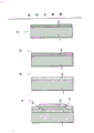
Polycrystalline SiTFT adopts the low temperature process manufacturing usually.As scheme shown in the IA, adopt low-pressure chemical vapor deposition method (LPCVD method), under 600 ℃ or lower temperature, polysilicon film 2 is deposited on the glass substrate 1.The fusing point of glass substrate is approximately 680 ℃ for instance.With Si
+In the ion implanted polysilicon film 2 of the inactive element of this class electrical property, to form the amorphous silicon film 3 shown in Figure 1B.Resulting structure is annealed 500 ℃ to 600 ℃ temperature, makes amorphous silicon film 3 solid state growths, so amorphous silicon film 3 produces crystallization.The result forms the polysilicon film 4 shown in Fig. 1 C, and its crystallite dimension (not shown) is bigger than the crystallite dimension of polysilicon film 2.Shown in Fig. 1 D, the predetermined position of polysilicon film 4 is corroded, thereby obtain predetermined figure.Adopt process for chemical vapor deposition of materials with via, under about 400 ℃ temperature, on resulting structure, deposit one deck (SiO
2) (silicon dioxide) film 5, make it cover whole surface.Subsequently, at SiO
2Sputter last layer M on the film 5
0The film 6 of (molybdenum) class.To M
0Film 6 and SiO
2The predetermined position of film 5 corrodes in succession, thereby forms the M with predetermined pattern
0Gate electrode 7 and by SiO
2The gate insulating film 8 that figure is formed, SiO
2The figure of dielectric film and M
0Gate electrode figure is identical.Subsequently, adopt ion implantation, make mask, will inject polysilicon film 4 (representing the phosphonium ion of polysilicon film 4 at Fig. 1 E with circle) with high concentration such as the n type impurity of phosphorus (P) with gate electrode 7 and gate insulating film 8.Resulting structure is annealed in about 600 ℃ temperature, so that the impurity electricity is activated, the result forms the n shown in Fig. 1 F
+Type source (district and drain region 9 and 10.Shown in Fig. 1 G, adopt process for chemical vapor deposition of materials with via, under about 400 ℃ of temperature, deposition one deck SiO
2 Film 11 is as passivating film, to cover whole surface.At last, to SiO
2The predetermined position of film 11 corrodes, and makes it form fairlead 11a and 11b.Al deposition is corroded at whole surperficial Shang , And,, make n type raceway groove polycrystalline SiTFT with this so that in fairlead 11a and 11b, form electrode 12 and 13.
The conventional method that adopts low temperature process to make polycrystalline SiTFT has following shortcoming.Impel the annealing process of the solid state growth of amorphous silicon film 3, must separate with the annealing process that impels the impurity electricity to activate, thereby make complex manufacturing processization to form source region and drain region 9 and 10.In addition, although there is the impurity that part ion injects at the crystal boundary place in polysilicon film 4, this part impurity that is positioned at the crystal boundary place is difficult to be activated by electricity by annealing process.Therefore, total activation efficiency of impurity is lower.Along with foreign ion injects polysilicon film 4, channelling can take place in dopant ion to a certain extent inevitably.Therefore, in annealing process subsequently, the impurity in source region and drain region 9 and 10 just can not be activated equably.
The prior art of thin-film transistor is illustrated in Japanese Applied Physics association the 45th lecture collected works (1984), and 14P-A-4 to 14P-A-6 number, the 407th to the 408th page.This piece list of references has been narrated owing to adopting ultra-thin polysilicon film technology to make the improvement of the polycrystalline SiTFT that transistor characteristic improved; Owing to adopt thermal oxidation technology, the improvement aspect solid-phase grain growth result and ultra-thin polysilicon film conductive characteristic; And adopt following technical process and the improvement of the transistor characteristic that obtains.This technical process is: form one deck Si with the plasma chemical vapor deposition method on ultra-thin polycrystalline SiTFT earlier
3N
4, then with the structure that obtains under 400 ℃ of temperature in hydrogen annealing.
The purpose of this invention is to provide a kind of method of making thin-film transistor, the method can be eliminated the shortcoming of above-mentioned conventional thin-film transistor.
In order to reach above-mentioned purpose of the present invention, the spy provides the method for making thin-film transistor as follows: form one deck polycrystalline semiconductor thin film on a substrate of being scheduled to; Predetermined ion is injected polycrystalline semiconductor thin film, to form one deck amorphous semiconductor films; On amorphous semiconductor films, form an one deck gate insulating film and a gate electrode; Utilize gate electrode and gate insulating film to mix, so that in amorphous semiconductor films, form source region and drain region as mask; Anneal,, simultaneously, the impurity electricity is activated, form source region and drain region to realize the solid state growth of amorphous semiconductor films.
By means of said method, impel the annealing process of amorphous semiconductor films solid state growth, needn't separate with the annealing process that impels the impurity electricity to activate to form source region and drain region.Therefore manufacturing process simplified.In addition, compare with the transistor of routine, the impurity in source region and drain region can be activated equably.
Figure 1A to 1G adopts traditional low temperature process to make the step cutaway view of conventional polycrystalline SiTFT in order to explanation.
Fig. 2 A to 2C adopts the cutaway view of making n raceway groove polycrystalline SiTFT step according to the method for embodiments of the invention making thin-film transistor in order to explanation.
Most preferred embodiment
Make the embodiment of thin-film transistor method as the present invention, special is example to make polycrystalline SiTFT, is illustrated with reference to accompanying drawing.In 2A to Fig. 2 C, all meet with Figure 1A to 1G in identical reference number, all represent identical part, no longer give a detailed account below.
Adopt the low-pressure chemical vapor deposition method, in about 580 ℃ to 600 ℃ temperature range, deposition one layer thickness for example is 800 on glass substrate 1
, the polysilicon film 2 same with Figure 1A.
With the 40Kev(kilo electron volt) acceleration energy be 1 * 10 with dosage
15/ (centimetre)
2To 5 * 10
15/ (centimetre)
2Si
+In the ion implanted polysilicon film 2, thereby form and the same amorphous silicon film 3 of Figure 1B.
Shown in Fig. 2 A, with the predetermined position corrosion of amorphous silicon film 3, with the figure that obtains to be scheduled to.Depositing a layer thickness with the low-pressure chemical vapor deposition method on whole exposed surface more for example is 1000
 , the SiO same with Fig. 1 D
2Film 5.At SiO
2Surface one layer thickness of
, the SiO same with Fig. 1 D
2Film 5.At SiO
2Surface one layer thickness of film 5 for example is 3000
 M
0Film 6.
M
0Film 6.
Shown in Fig. 2 B, M
0Film 6 and SiO
2The predetermined position of film 5 is corroded in succession, to form and same gate electrode 7 and the gate insulating film 8 of Fig. 1 E.After this, make mask with gate electrode 7 and gate insulating film 8, with P
+Ion injects amorphous silicon film 3 (phosphonium ion of representing amorphous silicon film 3 at Fig. 2 B with circle).
Annealing in process is to carry out under about 600 ℃ temperature, makes amorphous silicon film 3 solid state growths, to form the polysilicon film 4 of one deck shown in Fig. 2 C.Simultaneously, the phosphonium ion electricity of doping is activated, to form n
+Type source region and drain region 9 and 10.Form SiO then as passivating film
2Film 11 and electrode 12 and 13 are with the such n raceway groove polycrystalline SiTFT of preparation image pattern 1G.
According to the embodiment of introducing above as can be known, the solid state growth of amorphous silicon film 3 and the activation of impurity to form the process of source region and drain region 9 and 10, can realize in single annealing process.Therefore, compare, can save a step annealing technology, thereby simplify manufacturing process with the conventional method of Figure 1A to 1G.In above-mentioned annealing process, the activation of the solid state growth of amorphous silicon film 3 and the impurity of injection is carried out simultaneously.Therefore, compare with the transistor of routine, the impurity in source region and drain region 9 and 10 can be activated equably.
In above-mentioned annealing process, along with the solid state growth of amorphous silicon film 3, the phosphonium ion doped region that nucleus trends towards in film 3 forms.These nucleus grow into some small crystalss earlier, grow up to some big crystal grain then, therefore, compare with the transistor of routine, and the crystallite dimension in source region and drain region 9 and 10 has increased.So, because grain boundary area reduced than conventional transistor, so the degree that impurity will reduce along with grain boundary area and more effectively being activated.Utilize small crystals as seed crystal, crystal growth will be carried out along the direction on the surface that is parallel to amorphous silicon film 3.Utilize the above-mentioned solid phase growing method, at channel region 4a(Fig. 2 C) in the crystallite dimension of resulting polysilicon film 4, than in conventional transistor, being big.When thin-film transistor is worked, in channel region, will form raceway groove.Therefore, carrier mobility has been improved in the more conventional thin-film transistor of carrier mobility of the thin-film transistor of making of the present embodiment.
In the above-described embodiments, owing to adopt ion implantation that the impurity injection is occurred in Si to form source region and drain region 9 and 10 these processes
+Ion implanted polysilicon film 2 is with after formation amorphous silicon film 3 these processes, and therefore, the channelling of the impurity of injection can not take place basically.Vertically distribute according to the impurity that is injected in the prepared thin-film transistor of present embodiment, than in conventional thin-film transistor, just being even.So, the impurity in source region and drain region 9 and 10, comparable being activated more equably in conventional thin-film transistor.
Introduced certain embodiments of the present invention above, but this invention is not limited to this example.Within spirit of the present invention and scope, various changes can be made and modification.For example, can use such as F
+The ion of such electrical property inert element replaces Si
+Make source ion implantation, polysilicon film 2 is transformed into amorphous film.Form the source ion implantation of source region and drain region 9 and 10, also be not only limited to P
+, also can extend to the ion of other elements as required.Moreover the material of gate electrode 7 removes M
0Outside, also adopt tungsten such as W() such refractory metal, or refractory metal silicide.Polysilicon film 2 can replace with other polycrystalline semiconductor thin films.Polysilicon film 2 can replace the low-pressure chemical vapor deposition method to form such as glow discharge decomposition method (plasma CVD method) with other.Use glow discharge decomposition method, polysilicon film 2 can form under about 200 ℃ or lower temperature.
Claims (5)
1, a kind of method of making thin-film transistor is characterized in that: on a substrate of being scheduled to, form one deck polycrystalline semiconductor thin film; Predetermined ion is injected said polycrystalline semiconductor thin film, to form one deck amorphous semiconductor films; On said amorphous semiconductor films, form an one deck gate insulating film and a gate electrode; Utilize said gate electrode and gate insulating film to make mask, mix, so that in said amorphous semiconductor films, form source region and drain region; Anneal to realize the solid of said amorphous semiconductor films, the impurity electricity is activated, to form said source region and drain region to growth.
2, according to the method for claim 1, it is characterized in that: said polycrystalline semiconductor thin film comprises polysilicon film.
3, according to the method for claim 2, it is characterized in that: ion comprises that dosage is 1 * 10
15/ (centimetre)
2To 5 * 10
15/ (centimetre)
2Si
+Ion.
4, according to the method for claim 2 or 3, it is characterized in that: said polysilicon film forms when substrate temperature is 580 ℃ to 600 ℃ with the low-pressure chemical vapor deposition method.
5, according to claim 1,2,3 or 4 method is characterized in that: said predetermined substrate comprises glass substrate.
Applications Claiming Priority (2)
| Application Number | Priority Date | Filing Date | Title |
|---|---|---|---|
| JP59241239A JPH0824184B2 (en) | 1984-11-15 | 1984-11-15 | Method for manufacturing thin film transistor |
| JP241239/84 | 1984-11-15 |
Publications (1)
| Publication Number | Publication Date |
|---|---|
| CN85109088A true CN85109088A (en) | 1986-08-27 |
Family
ID=17071271
Family Applications (1)
| Application Number | Title | Priority Date | Filing Date |
|---|---|---|---|
| CN198585109088A Pending CN85109088A (en) | 1984-11-15 | 1985-11-15 | The manufacture method of thin-film transistor |
Country Status (7)
| Country | Link |
|---|---|
| JP (1) | JPH0824184B2 (en) |
| KR (1) | KR930010978B1 (en) |
| CN (1) | CN85109088A (en) |
| DE (1) | DE3540452C2 (en) |
| FR (1) | FR2573248B1 (en) |
| GB (1) | GB2167899B (en) |
| NL (1) | NL194524C (en) |
Cited By (4)
| Publication number | Priority date | Publication date | Assignee | Title |
|---|---|---|---|---|
| CN1293641C (en) * | 1992-12-09 | 2007-01-03 | 株式会社半导体能源研究所 | Electronic circuit |
| CN100461348C (en) * | 2004-07-21 | 2009-02-11 | 三星电子株式会社 | Silicon-based material layer, forming method, structure, device, emitter and display incorporating the silicon-based material layer |
| CN100559246C (en) * | 1992-05-29 | 2009-11-11 | 株式会社半导体能源研究所 | Active matrix liquid crystal display apparatus |
| CN104409635A (en) * | 2014-12-16 | 2015-03-11 | 京东方科技集团股份有限公司 | Organic thin film transistor and manufacturing method thereof, array substrate, and display unit |
Families Citing this family (5)
| Publication number | Priority date | Publication date | Assignee | Title |
|---|---|---|---|---|
| US5242507A (en) * | 1989-04-05 | 1993-09-07 | Boston University | Impurity-induced seeding of polycrystalline semiconductors |
| US5242858A (en) * | 1990-09-07 | 1993-09-07 | Canon Kabushiki Kaisha | Process for preparing semiconductor device by use of a flattening agent and diffusion |
| US5403756A (en) * | 1991-11-20 | 1995-04-04 | Sharp Kabushiki Kaisha | Method of producing a polycrystalline semiconductor film without annealing, for thin film transistor |
| KR950003235B1 (en) * | 1991-12-30 | 1995-04-06 | 주식회사 금성사 | Semiconductor device structure |
| US5985741A (en) | 1993-02-15 | 1999-11-16 | Semiconductor Energy Laboratory Co., Ltd. | Semiconductor device and method of fabricating the same |
Family Cites Families (5)
| Publication number | Priority date | Publication date | Assignee | Title |
|---|---|---|---|---|
| US4177084A (en) * | 1978-06-09 | 1979-12-04 | Hewlett-Packard Company | Method for producing a low defect layer of silicon-on-sapphire wafer |
| JPS558026A (en) * | 1978-06-30 | 1980-01-21 | Matsushita Electric Ind Co Ltd | Semi-conductor device manufacturing method |
| JPS5856409A (en) * | 1981-09-30 | 1983-04-04 | Toshiba Corp | Production of semiconductor device |
| JPS59165451A (en) * | 1983-03-11 | 1984-09-18 | Toshiba Corp | Manufacture of semiconductor device |
| JPS61191070A (en) * | 1985-02-20 | 1986-08-25 | Toshiba Corp | Manufacture of semiconductor device |
-
1984
- 1984-11-15 JP JP59241239A patent/JPH0824184B2/en not_active Expired - Lifetime
-
1985
- 1985-10-16 KR KR1019850007608A patent/KR930010978B1/en not_active IP Right Cessation
- 1985-11-11 GB GB08527737A patent/GB2167899B/en not_active Expired
- 1985-11-13 NL NL8503123A patent/NL194524C/en not_active IP Right Cessation
- 1985-11-14 DE DE3540452A patent/DE3540452C2/en not_active Expired - Fee Related
- 1985-11-15 CN CN198585109088A patent/CN85109088A/en active Pending
- 1985-11-15 FR FR858516906A patent/FR2573248B1/en not_active Expired - Lifetime
Cited By (7)
| Publication number | Priority date | Publication date | Assignee | Title |
|---|---|---|---|---|
| CN100559246C (en) * | 1992-05-29 | 2009-11-11 | 株式会社半导体能源研究所 | Active matrix liquid crystal display apparatus |
| CN1293641C (en) * | 1992-12-09 | 2007-01-03 | 株式会社半导体能源研究所 | Electronic circuit |
| CN100461348C (en) * | 2004-07-21 | 2009-02-11 | 三星电子株式会社 | Silicon-based material layer, forming method, structure, device, emitter and display incorporating the silicon-based material layer |
| CN104409635A (en) * | 2014-12-16 | 2015-03-11 | 京东方科技集团股份有限公司 | Organic thin film transistor and manufacturing method thereof, array substrate, and display unit |
| CN104409635B (en) * | 2014-12-16 | 2017-02-22 | 京东方科技集团股份有限公司 | Organic thin film transistor and manufacturing method thereof, array substrate, and display unit |
| US9728723B2 (en) | 2014-12-16 | 2017-08-08 | Boe Technology Group Co., Ltd. | Organic thin film transistor and manufacturing method thereof, array substrate |
| US10050200B2 (en) | 2014-12-16 | 2018-08-14 | Boe Technology Group Co., Ltd. | Organic thin film transistor and manufacturing method thereof, array substrate |
Also Published As
| Publication number | Publication date |
|---|---|
| GB2167899B (en) | 1988-04-27 |
| NL8503123A (en) | 1986-06-02 |
| JPH0824184B2 (en) | 1996-03-06 |
| FR2573248A1 (en) | 1986-05-16 |
| FR2573248B1 (en) | 1991-06-21 |
| NL194524C (en) | 2002-06-04 |
| JPS61119079A (en) | 1986-06-06 |
| KR860004455A (en) | 1986-06-23 |
| GB2167899A (en) | 1986-06-04 |
| KR930010978B1 (en) | 1993-11-18 |
| NL194524B (en) | 2002-02-01 |
| DE3540452C2 (en) | 1999-07-29 |
| DE3540452A1 (en) | 1986-06-05 |
| GB8527737D0 (en) | 1985-12-18 |
Similar Documents
| Publication | Publication Date | Title |
|---|---|---|
| CN1542929B (en) | Process for fabricating Semiconductor device | |
| US6620719B1 (en) | Method of forming ohmic contacts using a self doping layer for thin-film transistors | |
| US5970327A (en) | Method of fabricating a thin film transistor | |
| CN100399125C (en) | Device having thin film transistor | |
| EP0608503B1 (en) | A semiconductor device and its manufacturing method | |
| CN1186326A (en) | Manufacture of crystal semiconductor | |
| JP2947828B2 (en) | Method for manufacturing semiconductor device | |
| CN85109088A (en) | The manufacture method of thin-film transistor | |
| JPH06267978A (en) | Thin film transistor and manufacture thereof | |
| CN1146020C (en) | Method of forming singl-crystal silicon layer and method of manufacturing semiconductor device | |
| CN1666347A (en) | Tft electronic devices and their manufacture | |
| EP0481777A2 (en) | Method of manufacturing gate insulated field effect transistors | |
| KR930010093B1 (en) | Forming method of semiconductor thin film | |
| JP2523679B2 (en) | Thin film transistor and manufacturing method thereof | |
| KR960004902B1 (en) | Preparation of polycrystalline silicon thin film | |
| JPH0758334A (en) | Thin-film transistor | |
| JP3535465B2 (en) | Method for manufacturing semiconductor device | |
| KR100472855B1 (en) | Polycrystalline silicon thin film manufacturing method of semiconductor device | |
| KR100494321B1 (en) | Polycrystalline Silicon Film Formation Method of Semiconductor Device | |
| KR960013782B1 (en) | Manufacturing method of wiring device of semiconductor device | |
| JPH03132078A (en) | Semiconductor device and its manufacture | |
| JPH0786601A (en) | Polycrystalline silicon mos transistor and manufacture thereof | |
| JPH0554692B2 (en) | ||
| JPH01149475A (en) | Manufacture of thin film transistor | |
| JP3064363B2 (en) | Method of forming Si thin film |
Legal Events
| Date | Code | Title | Description |
|---|---|---|---|
| C06 | Publication | ||
| PB01 | Publication | ||
| WD01 | Invention patent application deemed withdrawn after publication |