CN1277458A - Producing method of relay base plate for installation of semi-conductor elements - Google Patents
Producing method of relay base plate for installation of semi-conductor elements Download PDFInfo
- Publication number
- CN1277458A CN1277458A CN00118082A CN00118082A CN1277458A CN 1277458 A CN1277458 A CN 1277458A CN 00118082 A CN00118082 A CN 00118082A CN 00118082 A CN00118082 A CN 00118082A CN 1277458 A CN1277458 A CN 1277458A
- Authority
- CN
- China
- Prior art keywords
- connection electrode
- motherboard
- lead wire
- conductor circuit
- metallide
- Prior art date
- Legal status (The legal status is an assumption and is not a legal conclusion. Google has not performed a legal analysis and makes no representation as to the accuracy of the status listed.)
- Granted
Links
Images


Classifications
-
- H—ELECTRICITY
- H05—ELECTRIC TECHNIQUES NOT OTHERWISE PROVIDED FOR
- H05K—PRINTED CIRCUITS; CASINGS OR CONSTRUCTIONAL DETAILS OF ELECTRIC APPARATUS; MANUFACTURE OF ASSEMBLAGES OF ELECTRICAL COMPONENTS
- H05K3/00—Apparatus or processes for manufacturing printed circuits
- H05K3/02—Apparatus or processes for manufacturing printed circuits in which the conductive material is applied to the surface of the insulating support and is thereafter removed from such areas of the surface which are not intended for current conducting or shielding
- H05K3/06—Apparatus or processes for manufacturing printed circuits in which the conductive material is applied to the surface of the insulating support and is thereafter removed from such areas of the surface which are not intended for current conducting or shielding the conductive material being removed chemically or electrolytically, e.g. by photo-etch process
-
- H—ELECTRICITY
- H05—ELECTRIC TECHNIQUES NOT OTHERWISE PROVIDED FOR
- H05K—PRINTED CIRCUITS; CASINGS OR CONSTRUCTIONAL DETAILS OF ELECTRIC APPARATUS; MANUFACTURE OF ASSEMBLAGES OF ELECTRICAL COMPONENTS
- H05K3/00—Apparatus or processes for manufacturing printed circuits
- H05K3/22—Secondary treatment of printed circuits
- H05K3/24—Reinforcing the conductive pattern
- H05K3/241—Reinforcing the conductive pattern characterised by the electroplating method; means therefor, e.g. baths or apparatus
- H05K3/242—Reinforcing the conductive pattern characterised by the electroplating method; means therefor, e.g. baths or apparatus characterised by using temporary conductors on the printed circuit for electrically connecting areas which are to be electroplated
-
- H10W70/05—
-
- H10W70/688—
-
- H—ELECTRICITY
- H05—ELECTRIC TECHNIQUES NOT OTHERWISE PROVIDED FOR
- H05K—PRINTED CIRCUITS; CASINGS OR CONSTRUCTIONAL DETAILS OF ELECTRIC APPARATUS; MANUFACTURE OF ASSEMBLAGES OF ELECTRICAL COMPONENTS
- H05K2203/00—Indexing scheme relating to apparatus or processes for manufacturing printed circuits covered by H05K3/00
- H05K2203/05—Patterning and lithography; Masks; Details of resist
- H05K2203/0562—Details of resist
- H05K2203/0571—Dual purpose resist, e.g. etch resist used as solder resist, solder resist used as plating resist
-
- H—ELECTRICITY
- H05—ELECTRIC TECHNIQUES NOT OTHERWISE PROVIDED FOR
- H05K—PRINTED CIRCUITS; CASINGS OR CONSTRUCTIONAL DETAILS OF ELECTRIC APPARATUS; MANUFACTURE OF ASSEMBLAGES OF ELECTRICAL COMPONENTS
- H05K2203/00—Indexing scheme relating to apparatus or processes for manufacturing printed circuits covered by H05K3/00
- H05K2203/05—Patterning and lithography; Masks; Details of resist
- H05K2203/0562—Details of resist
- H05K2203/058—Additional resists used for the same purpose but in different areas, i.e. not stacked
-
- H—ELECTRICITY
- H05—ELECTRIC TECHNIQUES NOT OTHERWISE PROVIDED FOR
- H05K—PRINTED CIRCUITS; CASINGS OR CONSTRUCTIONAL DETAILS OF ELECTRIC APPARATUS; MANUFACTURE OF ASSEMBLAGES OF ELECTRICAL COMPONENTS
- H05K2203/00—Indexing scheme relating to apparatus or processes for manufacturing printed circuits covered by H05K3/00
- H05K2203/05—Patterning and lithography; Masks; Details of resist
- H05K2203/0562—Details of resist
- H05K2203/0588—Second resist used as pattern over first resist
-
- H—ELECTRICITY
- H05—ELECTRIC TECHNIQUES NOT OTHERWISE PROVIDED FOR
- H05K—PRINTED CIRCUITS; CASINGS OR CONSTRUCTIONAL DETAILS OF ELECTRIC APPARATUS; MANUFACTURE OF ASSEMBLAGES OF ELECTRICAL COMPONENTS
- H05K3/00—Apparatus or processes for manufacturing printed circuits
- H05K3/02—Apparatus or processes for manufacturing printed circuits in which the conductive material is applied to the surface of the insulating support and is thereafter removed from such areas of the surface which are not intended for current conducting or shielding
- H05K3/06—Apparatus or processes for manufacturing printed circuits in which the conductive material is applied to the surface of the insulating support and is thereafter removed from such areas of the surface which are not intended for current conducting or shielding the conductive material being removed chemically or electrolytically, e.g. by photo-etch process
- H05K3/061—Etching masks
- H05K3/064—Photoresists
-
- H—ELECTRICITY
- H05—ELECTRIC TECHNIQUES NOT OTHERWISE PROVIDED FOR
- H05K—PRINTED CIRCUITS; CASINGS OR CONSTRUCTIONAL DETAILS OF ELECTRIC APPARATUS; MANUFACTURE OF ASSEMBLAGES OF ELECTRICAL COMPONENTS
- H05K3/00—Apparatus or processes for manufacturing printed circuits
- H05K3/22—Secondary treatment of printed circuits
- H05K3/28—Applying non-metallic protective coatings
Landscapes
- Engineering & Computer Science (AREA)
- Manufacturing & Machinery (AREA)
- Microelectronics & Electronic Packaging (AREA)
- Manufacturing Of Printed Wiring (AREA)
- Lead Frames For Integrated Circuits (AREA)
- Manufacturing Of Printed Circuit Boards (AREA)
- Printing Elements For Providing Electric Connections Between Printed Circuits (AREA)
- Wire Bonding (AREA)
Abstract
按照本发明,不使用冲模以机械方式在中继基板上开孔,利用刻蚀使各母板连接电极在导电性方面互相独立,而且能尽可能缩短电镀引线。
According to the present invention, holes are mechanically opened on the relay substrate without using a punching die, the electrical conductivity of each motherboard connection electrode is made independent of each other by etching, and the electroplating lead can be shortened as much as possible.
Description
The present invention relates to for semiconductor element mounting to motherboard and the semiconductor element mounting of using with the manufacture method of relaying substrate.
In recent years, the miniaturization, the lightweight that possess the electronic installation of semiconductor element make progress, according to this trend, carrying out following work: with semiconductor element mounting on its size and the identical substantially circuit substrate that is called insertion plate (interposer) of this semiconductor element (promptly, semiconductor element mounting relaying substrate), make the packaging body (CSP) of chip size, then this packaging body is installed on the motherboard.
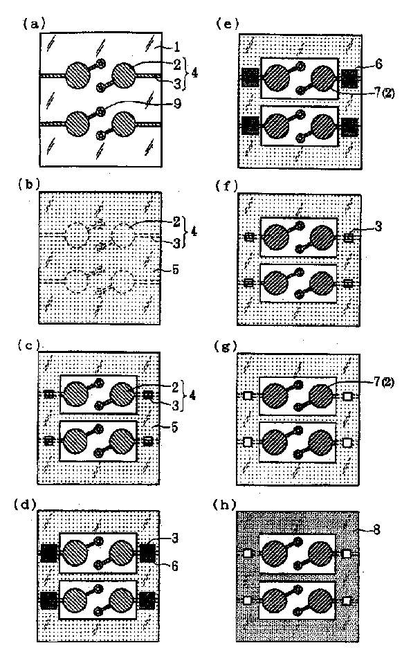
Make such semiconductor element mounting relaying substrate as shown in Figure 3 like that.
At first, form conductor circuit 34 on insulating properties matrix material film 31, this conductor circuit 34 comprises: the motherboard connection electrode 32 that is connected usefulness with motherboard; And for motherboard connection electrode 32 being carried out metallide is handled and with the electroplate lead wire 33 (Fig. 3 (a)) of motherboard connection electrode 32 conductings.The continuous conductor portion 31a conducting of the two edges of electroplate lead wire 33 and insulating properties basis material diaphragm 31.
Have again, formed the through hole 35 on the semiconductor element (not shown) that is used for motherboard connection electrode 32 is guided to the back side in semiconductor element mounting on the relaying substrate.
Secondly, conductor circuit 34 is carried out metallide handle, at least stacked metallide metal level 36 (Fig. 3 (b)) on motherboard connection electrode 32.
Secondly, use punch die near motherboard connection electrode 32, to leave hole 37 and cut off electroplate lead wire, so that shorten electroplate lead wire 33 (Fig. 3 (c)) as far as possible.As required excise the continuous conductor portion 31a (Fig. 3 (d)) of the two edges of insulating properties matrix material film 31 thereafter.
As shown in Fig. 3 (c), the reason of cut-out electroplate lead wire 33 is as follows near motherboard connection electrode 32.
Promptly, under the long situation of the length of on the insulating properties matrix material film 31 and electroplate lead wires 33 each motherboard connection electrode 32 conducting, because the cause of branch's wiring this respect, produce reflecting background, in addition, because the cause of redundant wiring this respect, reactance or electric capacity become big, the electrical characteristics of semiconductor element descend.In addition, must make each motherboard connection electrode 32 independent mutually aspect conductivity.Thereby, in order to make semiconductor element mounting relaying substrate expeditiously, after each motherboard connection electrode 32 having been carried out the metallide processing, use punch die near each motherboard connection electrode 32, to leave hole 37, so that shorten electroplate lead wire 33 as far as possible.
But, using punch die to leave under the situation in hole, produce the setation thorn sometimes at the edge in hole, cause bad order or at aspect of performance generation obstacle.In addition, when making CSP, if then there is the resin-sealed problem that becomes difficult in perforate on circuit substrate.In addition, on the polyimide matrix material membrane that little CSP uses with good precision and also under the situation of not damaging matrix material film mechanically the operation of perforate be not simple.And, also need higher cost at the manufacture view of punch die.
The present invention carries out in order to solve above existing technical task, its purpose is, in the semiconductor element mounting of making substrate that CSP uses etc. during with the relaying substrate, do not use punch die mechanically to come perforate, can make each motherboard connection electrode independent mutually aspect conductivity, and can shorten electroplate lead wire as far as possible.
The present inventor has found, in the manufacturing process of semiconductor element mounting with the relaying substrate, if can utilize etching to excise to be installed to the electroplate lead wire of the relaying real estate of motherboard one side, then can solve above-mentioned problem, and found, in order to reach this purpose, the composition that can carry out etching with chemical mode with resin bed (for example, can carry out the polyimide precursor layer (polyamic acid layer etc.) of etching with alkaline solution, the photosensitive polyimide layer, etching resist when the photoresist layer) conduct is excised electroplate lead wire in the etching mode utilizes and gets final product, and has finished the present invention.
Promptly, the 1st aspect of the present invention be for semiconductor element mounting to motherboard and the semiconductor element mounting of using with the manufacture method of relaying substrate, a kind of manufacture method that is characterised in that the semiconductor element mounting that comprises following operation (A)~(G) with the relaying substrate is provided:
(A) on the insulating properties matrix material film, form the operation of conductor circuit, this conductor circuit comprise the motherboard connection electrode that is connected usefulness with motherboard and for this motherboard connection electrode being carried out the metallide processing with the electroplate lead wire of this motherboard connection electrode conducting;
(B) on this conductor circuit, form the operation of composition with resin bed;
(C) this composition of etching with resin bed so that expose the motherboard connection electrode of this conductor circuit and the operation of electroplate lead wire;
(D) cover the operation of the electroplate lead wire exposed with the metallide resist layer;
(E) the motherboard connection electrode of having exposed is carried out metallide is handled, the operation of stacked metallide metal level on the motherboard connection electrode;
(F) remove the metallide resist layer that has covered electroplate lead wire, the operation that electroplate lead wire is exposed once more; And
(G) operation of the electroplate lead wire that utilizes etching to remove to have exposed.
In addition, the 2nd aspect of the present invention be for semiconductor element mounting to motherboard and the semiconductor element mounting of using with the manufacture method of relaying substrate, a kind of manufacture method that is characterised in that the semiconductor element mounting that comprises following operation (a)~(f) with the relaying substrate is provided:
(a) on the insulating properties matrix material film, form the operation of conductor circuit, this conductor circuit comprise the motherboard connection electrode that is connected usefulness with motherboard and for this motherboard connection electrode being carried out the metallide processing with the electroplate lead wire of this motherboard connection electrode conducting;
(b) on this conductor circuit, form the operation of composition with resin bed;
(c) this composition of etching with resin bed so that expose the operation of the motherboard connection electrode of this conductor circuit;
(d) the motherboard connection electrode of having exposed is carried out metallide is handled, the operation of stacked metallide metal level on the motherboard connection electrode;
(e) this composition of etching with resin bed so that expose the operation of the electroplate lead wire of this conductor circuit; And
(f) operation of the electroplate lead wire that utilizes etching to remove to have exposed.
Fig. 1 is the manufacturing procedure picture of semiconductor element mounting of the present invention with the relaying substrate.
Fig. 2 is the manufacturing procedure picture of semiconductor element mounting of the present invention with the relaying substrate.
Fig. 3 is that the conventional semiconductor element is installed the manufacturing procedure picture with the relaying substrate.
At first, on one side with reference to accompanying drawing, by each operation the manufacture method of the semiconductor element mounting of the 1st aspect of the present invention with the relaying substrate is described on one side.
Operation (A)
At first, on insulating properties matrix material film 1, form conductor circuit 4, this conductor circuit 4 comprise the motherboard connection electrode 2 that is connected usefulness with motherboard (not shown) and for this motherboard connection electrode 2 being carried out the metallide processing with the electroplate lead wire 3 (Fig. 1 (a)) of these motherboard connection electrode 2 conductings.Have, electroplate lead wire 3 can connect with conductor portion continuous on the two edges of insulating properties matrix material film 1 (not shown, with reference to the 31a of Fig. 3 (a) of prior art) again.Electrode when this zone becomes electroplating processes described later.
Have again, usually, on the conductor circuit 4 of semiconductor element mounting, be provided with the through hole 9 (Fig. 1 (a)) that is used for making motherboard connection electrode 2 and the another side conducting of insulating properties matrix material film 1, on the another side of insulating properties matrix material film 1, formed the IC chip that is used for installing semiconductor element and installed with salient point (not shown) with the relaying substrate.
Can utilize conventional method to form such conductor circuit 4.For example, at first, utilize conventional method that the copper layer that the single face of having pasted the copper layer on the polyimide insulative film applies the copper flexible base, board is carried out composition,, this salient point is formed face (semiconductor element mounting face) carry out masked operation forming as required after the IC chip installs with salient point.Secondly, after having left the hole that through hole uses on the polyimide insulative film, on whole, carry out electrolytic copper free electroplating and handle, then, utilize of the thickness thickening of cathode copper electroplating processes copper.Secondly, stacked photosensitive dry film on the surface of this cathode copper layer exposes, develops by the photomask corresponding with wired circuit, forms the etching resist layer, utilizing copper chloride or iron chloride etching liquid to carry out after the etching, utilizing conventional method to remove the etching resist layer and get final product.
Operation (B)
On conductor circuit 4, form composition resin bed 5 (Fig. 1 (b)).With resin bed 5, can use polyimide precursor layer 5, photosensitive polyimide layer, photoresist layer etc. as composition.Wherein, because polyimide precursor layer can dissolve in alkaline solution, so is the layer that can carry out composition, be simultaneously can utilize imidization handle (for example, heat treated) harden and be transformed into polyimide layer good aspect thermal endurance, chemical proofing layer.As such polyimide precursor layer, can form by utilizing the known polyamic acids of coating such as heliogravure applicator to apply liquid and carry out drying.
Operation (C)
Secondly, according to conventional method etching composition resin bed 5, so that expose the motherboard connection electrode 2 and the electroplate lead wire 3 (Fig. 1 (c)) of conductor circuit 4.For example, with stacked photosensitive dry film on the resin bed 5, the photomask of the shape by regulation exposes, develops, formation etching resist layer at composition, utilizing sodium hydrate aqueous solution etc. to carry out after the etching, utilize conventional method to remove the etching resist layer and get final product.
Operation (D)
Cover the electroplate lead wire 3 (Fig. 1 (d)) that has exposed with common metallide resist layer 6.At this moment, do not cover motherboard connection electrode 2.
Operation (E)
Secondly, the motherboard connection electrode of having exposed 2 is carried out metallide and handle (for example, electrolysis gold electroplating processes), stacked metallide metal level 7 on motherboard connection electrode 2 (Fig. 1 (e)).Thus, the solder ball that the application ball-shaped grid array is used on motherboard connection electrode 2 becomes easy.
Operation (F)
Secondly, remove the metallide resist layer 6 that covers electroplate lead wire 3, make electroplate lead wire 3 expose (Fig. 1 (f)) once more.
Operation (G)
Secondly, utilize the etching liquid of copper chloride or iron chloride etching liquid etc. to remove the electroplate lead wire 3 (Fig. 1 (g)) that has exposed.At this moment, make metallide metal level 7 play function as the etching resist of the motherboard connection electrode 2 of its lower floor.For this reason, forming metallide metal level 7 with the material (for example, gold) of performance with anti-etching liquid gets final product.Perhaps, pre-determine situation about being etched, in advance metallide metal level 7 is formed thicker getting final product.Thus, the contraction in length of the electroplate lead wire that can will be connected with the motherboard connection electrode 2 of metallide metal level 7 and lower floor thereof at the formation in-process of a series of conductor circuit 4 is not handled and do not use punch die to carry out perforate to bottom line.
Operation (H)
Secondly, be under the situation of polyimide precursor layer at composition resin bed 5, make the imidization fully of this polyimide precursor layer, become polyimide layer 8, thus, can obtain such semiconductor element mounting relaying substrate shown in Fig. 1 (h).Have, this operation (H) (imidization of polyimide precursor layer) can be implemented in operation (G) back again, but also can promptly, implement between operation (C) and operation (D) behind the composition of polyimide precursor layer.
As mentioned above, the 1st aspect of the present invention is characterised in that, utilizes etching to cut off the electroplate lead wire of semiconductor element mounting with the surface that is installed to motherboard one side of relaying substrate, thereby, about the installed surface of the semiconductor element of relaying substrate and the formation method of through hole, can utilize prior art.
Have, in the manufacture method aspect the above the of the present invention the 1st, composition carries out 1 time with the composition (operation (C)) of resin bed 5, but as shown below, also can carry out 2 times (operation (c) and operation (e)) as the 2nd aspect of the present invention again.
Operation (a)
Identical with the operation (A) of the 1st aspect of the present invention, at first, on insulating properties matrix material film 1, form conductor circuit 4, this conductor circuit 4 comprise that the motherboard that is connected usefulness with motherboard connects electroplax 2 and for this motherboard connection electrode 2 being carried out the metallide processing with the electroplate lead wire 3 (Fig. 2 (a)) of motherboard connection electrode 2 conductings.Have, electroplate lead wire 3 can connect with conductor portion continuous on the two edges of insulating properties matrix material film 1 (not shown, with reference to the 31a of Fig. 3 (a) of prior art) again.Electrode when this zone becomes electroplating processes described later.
Operation (b)
Secondly, identical with the operation (B) of the 1st aspect of the present invention, the composition that forms polyimide precursor layer etc. on conductor circuit 4 is with resin bed 5 (Fig. 2 (b)).
Operation (c)
Secondly, according to the operation (C) of the 1st aspect of the present invention, the etching composition is with resin bed 5, so that expose the motherboard connection electrode 2 (Fig. 2 (c)) of conductor circuit 4.At this moment, different with the 1st aspect of the present invention, carry out etching like this, electroplate lead wire 3 is not exposed.
Operation (d)
Secondly, according to the operation (E) of the 1st aspect of the present invention, the motherboard connection electrode of having exposed 2 is carried out metallide handle stacked metallide metal level 7 on motherboard connection electrode 2 (Fig. 2 (d)).
Operation (e)
Secondly, according to the operation (C) of the 1st aspect of the present invention, the etching composition is with resin bed 5, so that expose the electroplate lead wire 3 (Fig. 2 (e)) of conductor circuit 4.
Operation (f)
Secondly, according to the operation (G) of the 1st aspect of the present invention, the electroplate lead wire 3 (Fig. 2 (f)) that utilizes etching to remove to have exposed.
Operation (g)
Secondly, identical with the operation (H) of the 1st aspect of the present invention, be under the situation of polyimide precursor layer at composition resin bed 5, with the imidization fully of this polyimide precursor layer, become polyimide layer 8, thus, can obtain such semiconductor element mounting relaying substrate shown in Fig. 2 (g).
Have again, aspect the of the present invention the 2nd in, can be between operation (c) and operation (d), as operation (h) and then be provided with, make the polyimide precursor layer operation of imidization by halves.This incomplete degree is decided to be such degree, that is, by adjusting imidization condition (heating-up temperature, heating time etc.), polyimide precursor layer is injury-free under the implementation condition of its follow-up operation, but can carry out the composition of itself.Thereby, by the incomplete imidization operation of such polyimide precursor layer is set, can improve the dimensional accuracy of conductor circuit 4, can improve the fabrication yield of relaying substrate.
As mentioned above, the 2nd aspect of the present invention is characterised in that, utilize etching to cut off the electroplate lead wire of semiconductor element mounting with the surface that is installed to motherboard one side of relaying substrate, thereby, about the installed surface of the semiconductor element of relaying substrate and the formation method of through hole, identical with the 1st aspect of the present invention, can utilize prior art.
According to the present invention, in the semiconductor element mounting of making substrate that CSP uses etc. during with the relaying substrate, do not use mechanically perforate on the relaying substrate of punch die, can utilize etching to make each motherboard connection electrode independent mutually aspect conductivity, and can shorten electroplate lead wire as far as possible.
Claims (7)
- One kind for semiconductor element mounting to motherboard and the semiconductor element mounting of using with the manufacture method of relaying substrate, it is characterized in that, comprise following operation (A)~(G):(A) on the insulating properties matrix material film, form the operation of conductor circuit, this conductor circuit comprise the motherboard connection electrode that is connected usefulness with motherboard and for this motherboard connection electrode being carried out the metallide processing with the electroplate lead wire of this motherboard connection electrode conducting;(B) on this conductor circuit, form the operation of composition with resin bed;(C) this composition of etching with resin bed so that expose the motherboard connection electrode of this conductor circuit and the operation of electroplate lead wire;(D) cover the operation of the electroplate lead wire exposed with the metallide resist layer;(E) the motherboard connection electrode of having exposed is carried out metallide is handled, the operation of stacked metallide metal level on the motherboard connection electrode;(F) remove the metallide resist layer that has covered electroplate lead wire, the operation that electroplate lead wire is exposed once more; And(G) operation of the electroplate lead wire that utilizes etching to remove to have exposed.
- 2. the manufacture method described in claim 1 is characterized in that:The composition resin bed is a polyimide precursor layer.
- 3. the manufacture method described in claim 2 is characterized in that:Between operation (C) and operation (D) or after operation (G), comprise following operation (H),(H) make the operation of polyimide precursor layer imidization fully.
- One kind for semiconductor element mounting to motherboard and the semiconductor element mounting of using with the manufacture method of relaying substrate, it is characterized in that, comprise following operation (a)~(f):(a) on the insulating properties matrix material film, form the operation of conductor circuit, this conductor circuit comprise the motherboard connection electrode that is connected usefulness with motherboard and for this motherboard connection electrode being carried out the metallide processing with the electroplate lead wire of this motherboard connection electrode conducting;(b) on this conductor circuit, form the operation of composition with resin bed;(c) this composition of etching with resin bed so that expose the operation of the motherboard connection electrode of this conductor circuit;(d) the motherboard connection electrode of having exposed is carried out metallide is handled, the operation of stacked metallide metal level on the motherboard connection electrode;(e) this composition of etching with resin bed so that expose the operation of the electroplate lead wire of this conductor circuit; And(f) operation of the electroplate lead wire that utilizes etching to remove to have exposed.
- 5. the manufacture method described in claim 4 is characterized in that:The composition resin bed is a polyimide precursor layer.
- 6. the manufacture method described in claim 5 is characterized in that:After operation (f), also comprise operation (g),(g) make the operation of polyimide precursor layer imidization fully.
- 7. the manufacture method described in claim 6 is characterized in that:Between operation (c) and the operation (d) or between operation (d) and operation (e), also comprise operation (h),(h) make the polyimide precursor layer operation of imidization by halves.
Applications Claiming Priority (2)
| Application Number | Priority Date | Filing Date | Title |
|---|---|---|---|
| JP164148/1999 | 1999-06-10 | ||
| JP11164148A JP2000353760A (en) | 1999-06-10 | 1999-06-10 | Method for manufacturing relay substrate for mounting semiconductor element |
Publications (2)
| Publication Number | Publication Date |
|---|---|
| CN1277458A true CN1277458A (en) | 2000-12-20 |
| CN1149649C CN1149649C (en) | 2004-05-12 |
Family
ID=15787664
Family Applications (1)
| Application Number | Title | Priority Date | Filing Date |
|---|---|---|---|
| CNB001180827A Expired - Lifetime CN1149649C (en) | 1999-06-10 | 2000-06-09 | Manufacturing method of interposer substrate for mounting semiconductor element |
Country Status (5)
| Country | Link |
|---|---|
| US (1) | US6312614B1 (en) |
| JP (1) | JP2000353760A (en) |
| KR (1) | KR100783340B1 (en) |
| CN (1) | CN1149649C (en) |
| TW (1) | TW521417B (en) |
Cited By (5)
| Publication number | Priority date | Publication date | Assignee | Title |
|---|---|---|---|---|
| CN100424844C (en) * | 2002-02-08 | 2008-10-08 | 三星电机株式会社 | Method for manufacturing printed circuit board strips |
| CN100459079C (en) * | 2005-12-12 | 2009-02-04 | 精工爱普生株式会社 | Manufacturing method of wiring substrate |
| CN100547778C (en) * | 2006-02-23 | 2009-10-07 | 艾格瑞系统有限公司 | Flexible circuit substrate and method of forming and assembly including flexible circuit substrate |
| CN101861054A (en) * | 2010-04-08 | 2010-10-13 | 冠锋电子科技(梅州)有限公司 | Method for removing goldplated plug lead wires |
| CN104347780A (en) * | 2013-08-06 | 2015-02-11 | 惠州市华阳光电技术有限公司 | Substrate of chip on board and manufacturing process thereof |
Families Citing this family (16)
| Publication number | Priority date | Publication date | Assignee | Title |
|---|---|---|---|---|
| JP3357875B1 (en) | 2001-06-29 | 2002-12-16 | 株式会社リョウワ | Electroplating method and method for manufacturing printed wiring board |
| KR100476409B1 (en) * | 2002-06-07 | 2005-03-16 | 엘지전자 주식회사 | Plating method for PCB |
| EP1381259A1 (en) * | 2002-07-11 | 2004-01-14 | Ultratera Corporation | Structure of printed circuit board (PCB) |
| KR20050050849A (en) * | 2003-11-26 | 2005-06-01 | 삼성전기주식회사 | Fabricating method of printed circuit board without electrolytic plating lead |
| TWI237534B (en) * | 2004-05-07 | 2005-08-01 | Advanced Semiconductor Eng | Fabrication method of a printed circuit board |
| US7105918B2 (en) * | 2004-07-29 | 2006-09-12 | Micron Technology, Inc. | Interposer with flexible solder pad elements and methods of manufacturing the same |
| JP2008181702A (en) * | 2007-01-23 | 2008-08-07 | Mitsumi Electric Co Ltd | Battery pack, battery protection module, and method for manufacturing battery protection module substrate |
| TWI334320B (en) * | 2007-07-16 | 2010-12-01 | Nanya Technology Corp | Fabricating method of gold finger of circuit board |
| JP2009147270A (en) * | 2007-12-18 | 2009-07-02 | Nec Electronics Corp | Wiring board manufacturing method, wiring board, and semiconductor device |
| JP5188289B2 (en) * | 2008-06-26 | 2013-04-24 | ラピスセミコンダクタ株式会社 | Method for manufacturing printed circuit board |
| JP5334607B2 (en) * | 2008-12-25 | 2013-11-06 | 京セラ株式会社 | WIRING BOARD, WIRING BOARD MANUFACTURING METHOD, AND PROBE CARD |
| TWI560840B (en) * | 2014-10-30 | 2016-12-01 | Winbond Electronics Corp | Flexible microsystem structure |
| US9412692B2 (en) | 2015-01-13 | 2016-08-09 | Winbond Electronics Corp. | Flexible microsystem structure |
| CA3018405A1 (en) * | 2016-03-22 | 2017-09-28 | Jun Yang | Method for solvent-free printing conductors on substrate |
| KR102050939B1 (en) | 2019-10-15 | 2020-01-08 | 주식회사 동원파츠 | Metho for manufacturing repeater using friction stir welding |
| CN111065210A (en) * | 2019-12-25 | 2020-04-24 | 上海嘉捷通电路科技股份有限公司 | Method for replacing manual PCB (printed circuit board) process lead wire picking |
Family Cites Families (11)
| Publication number | Priority date | Publication date | Assignee | Title |
|---|---|---|---|---|
| JPS6318355A (en) | 1986-07-10 | 1988-01-26 | Konica Corp | Electrophotographic sensitive body |
| JPH04109693A (en) * | 1990-08-30 | 1992-04-10 | Tanaka Kikinzoku Kogyo Kk | Manufacturing method of platinum circuit board |
| US5480048A (en) * | 1992-09-04 | 1996-01-02 | Hitachi, Ltd. | Multilayer wiring board fabricating method |
| US5509553A (en) * | 1994-04-22 | 1996-04-23 | Litel Instruments | Direct etch processes for the manufacture of high density multichip modules |
| JPH0951155A (en) | 1995-08-08 | 1997-02-18 | Mitsui Toatsu Chem Inc | Method of forming solder mask |
| US5733466A (en) * | 1996-02-06 | 1998-03-31 | International Business Machines Corporation | Electrolytic method of depositing gold connectors on a printed circuit board |
| DE19610723A1 (en) * | 1996-03-19 | 1997-09-25 | Bayer Ag | Electroluminescent devices using glare systems |
| JPH1070353A (en) * | 1996-08-26 | 1998-03-10 | Sumitomo Metal Mining Co Ltd | Manufacturing method of electronic circuit board using copper-coated polyimide substrate |
| JPH10188817A (en) * | 1996-12-25 | 1998-07-21 | Canon Inc | Element circuit board, image forming apparatus and method of manufacturing the same |
| JPH1117331A (en) * | 1997-06-26 | 1999-01-22 | Nippon Mektron Ltd | Manufacture of flexible circuit board |
| KR980000010A (en) * | 1997-10-20 | 1998-03-30 | 유연광 | How to grow buckwheat |
-
1999
- 1999-06-10 JP JP11164148A patent/JP2000353760A/en active Pending
-
2000
- 2000-05-25 US US09/577,883 patent/US6312614B1/en not_active Expired - Fee Related
- 2000-05-29 TW TW089110389A patent/TW521417B/en not_active IP Right Cessation
- 2000-06-07 KR KR1020000031053A patent/KR100783340B1/en not_active Expired - Lifetime
- 2000-06-09 CN CNB001180827A patent/CN1149649C/en not_active Expired - Lifetime
Cited By (6)
| Publication number | Priority date | Publication date | Assignee | Title |
|---|---|---|---|---|
| CN100424844C (en) * | 2002-02-08 | 2008-10-08 | 三星电机株式会社 | Method for manufacturing printed circuit board strips |
| CN100459079C (en) * | 2005-12-12 | 2009-02-04 | 精工爱普生株式会社 | Manufacturing method of wiring substrate |
| CN100547778C (en) * | 2006-02-23 | 2009-10-07 | 艾格瑞系统有限公司 | Flexible circuit substrate and method of forming and assembly including flexible circuit substrate |
| CN101861054A (en) * | 2010-04-08 | 2010-10-13 | 冠锋电子科技(梅州)有限公司 | Method for removing goldplated plug lead wires |
| CN104347780A (en) * | 2013-08-06 | 2015-02-11 | 惠州市华阳光电技术有限公司 | Substrate of chip on board and manufacturing process thereof |
| CN104347780B (en) * | 2013-08-06 | 2018-12-04 | 惠州市华阳光电技术有限公司 | A kind of substrate and its manufacturing process of chip on board |
Also Published As
| Publication number | Publication date |
|---|---|
| CN1149649C (en) | 2004-05-12 |
| US6312614B1 (en) | 2001-11-06 |
| KR20010007271A (en) | 2001-01-26 |
| TW521417B (en) | 2003-02-21 |
| JP2000353760A (en) | 2000-12-19 |
| KR100783340B1 (en) | 2007-12-07 |
Similar Documents
| Publication | Publication Date | Title |
|---|---|---|
| CN1277458A (en) | Producing method of relay base plate for installation of semi-conductor elements | |
| CN1197137C (en) | Semiconductor device and method for manufacture semiconductor equipment | |
| CN1254859C (en) | Manufacturing method of circuit device | |
| CN1520250A (en) | Method for interconnecting multilayer printed circuit boards | |
| JP2004013738A5 (en) | ||
| CN102165582B (en) | Lead frame substrate, manufacturing method thereof, and semiconductor device | |
| CN1643691A (en) | Semiconductor die package with semiconductor die having side electrical connection | |
| CN1377219A (en) | Method for manufacturing a circuit device | |
| CN1191619C (en) | Circuit device and its producing method | |
| CN1335740A (en) | Wiring circuit board with projecture and its producing method | |
| CN1212786A (en) | Semiconductor device and manufacturing method thereof | |
| CN1327265A (en) | Lead wire frame, semiconductor and its producing method, circuit base board and electronic device | |
| CN1369912A (en) | Semiconductor integrated circuit and its preparing method | |
| CN1231971C (en) | Surface installation type chip semiconductor device and making method thereof | |
| CN1392600A (en) | Method for producing circuit device | |
| CN1497688A (en) | Method for manufacturing a circuit device | |
| CN1364051A (en) | Flexible distributing board and manufacture thereof | |
| CN115190701A (en) | Embedded circuit packaging substrate and processing method thereof | |
| CN1494369A (en) | Electroplating method of prited circuit board | |
| CN1139984C (en) | semiconductor device, assembling method, and circuit baseboard and soft baseboard and mfg. method therefor | |
| JPH1140720A (en) | Circuit member and resin-sealed semiconductor device using the circuit member | |
| US20070269929A1 (en) | Method of reducing stress on a semiconductor die with a distributed plating pattern | |
| JP2003332503A (en) | Circuit board having heat sink and manufacturing method thereof | |
| CN113113319A (en) | Lead frame and manufacturing method thereof | |
| CN1146986C (en) | Semiconductor chip package and its packaging method |
Legal Events
| Date | Code | Title | Description |
|---|---|---|---|
| C06 | Publication | ||
| PB01 | Publication | ||
| C10 | Entry into substantive examination | ||
| SE01 | Entry into force of request for substantive examination | ||
| C14 | Grant of patent or utility model | ||
| GR01 | Patent grant | ||
| CX01 | Expiry of patent term |
Granted publication date: 20040512 |
|
| CX01 | Expiry of patent term |