CN1160761C - 样品加工系统 - Google Patents
样品加工系统 Download PDFInfo
- Publication number
- CN1160761C CN1160761C CNB991234332A CN99123433A CN1160761C CN 1160761 C CN1160761 C CN 1160761C CN B991234332 A CNB991234332 A CN B991234332A CN 99123433 A CN99123433 A CN 99123433A CN 1160761 C CN1160761 C CN 1160761C
- Authority
- CN
- China
- Prior art keywords
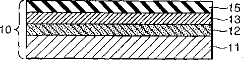
- substrate
- sheet
- sample
- separation
- layer
- Prior art date
- Legal status (The legal status is an assumption and is not a legal conclusion. Google has not performed a legal analysis and makes no representation as to the accuracy of the status listed.)
- Expired - Fee Related
Links
Images


Classifications
-
- H—ELECTRICITY
- H10—SEMICONDUCTOR DEVICES; ELECTRIC SOLID-STATE DEVICES NOT OTHERWISE PROVIDED FOR
- H10P—GENERIC PROCESSES OR APPARATUS FOR THE MANUFACTURE OR TREATMENT OF DEVICES COVERED BY CLASS H10
- H10P72/00—Handling or holding of wafers, substrates or devices during manufacture or treatment thereof
- H10P72/04—Apparatus for manufacture or treatment
- H10P72/0451—Apparatus for manufacturing or treating in a plurality of work-stations
- H10P72/0452—Apparatus for manufacturing or treating in a plurality of work-stations characterised by the layout of the process chambers
- H10P72/0454—Apparatus for manufacturing or treating in a plurality of work-stations characterised by the layout of the process chambers surrounding a central transfer chamber
-
- H—ELECTRICITY
- H10—SEMICONDUCTOR DEVICES; ELECTRIC SOLID-STATE DEVICES NOT OTHERWISE PROVIDED FOR
- H10P—GENERIC PROCESSES OR APPARATUS FOR THE MANUFACTURE OR TREATMENT OF DEVICES COVERED BY CLASS H10
- H10P14/00—Formation of materials, e.g. in the shape of layers or pillars
- H10P14/20—Formation of materials, e.g. in the shape of layers or pillars of semiconductor materials
-
- H—ELECTRICITY
- H10—SEMICONDUCTOR DEVICES; ELECTRIC SOLID-STATE DEVICES NOT OTHERWISE PROVIDED FOR
- H10P—GENERIC PROCESSES OR APPARATUS FOR THE MANUFACTURE OR TREATMENT OF DEVICES COVERED BY CLASS H10
- H10P72/00—Handling or holding of wafers, substrates or devices during manufacture or treatment thereof
- H10P72/04—Apparatus for manufacture or treatment
- H10P72/0428—Apparatus for mechanical treatment or grinding or cutting
Landscapes
- Container, Conveyance, Adherence, Positioning, Of Wafer (AREA)
- Weting (AREA)
Applications Claiming Priority (2)
| Application Number | Priority Date | Filing Date | Title |
|---|---|---|---|
| JP31657598A JP4343295B2 (ja) | 1998-11-06 | 1998-11-06 | 試料の処理システム |
| JP316575/1998 | 1998-11-06 |
Publications (2)
| Publication Number | Publication Date |
|---|---|
| CN1258091A CN1258091A (zh) | 2000-06-28 |
| CN1160761C true CN1160761C (zh) | 2004-08-04 |
Family
ID=18078631
Family Applications (1)
| Application Number | Title | Priority Date | Filing Date |
|---|---|---|---|
| CNB991234332A Expired - Fee Related CN1160761C (zh) | 1998-11-06 | 1999-11-05 | 样品加工系统 |
Country Status (5)
| Country | Link |
|---|---|
| EP (1) | EP0999578A3 (https=) |
| JP (1) | JP4343295B2 (https=) |
| KR (1) | KR100444262B1 (https=) |
| CN (1) | CN1160761C (https=) |
| TW (1) | TW459299B (https=) |
Families Citing this family (16)
| Publication number | Priority date | Publication date | Assignee | Title |
|---|---|---|---|---|
| EP0989593A3 (en) * | 1998-09-25 | 2002-01-02 | Canon Kabushiki Kaisha | Substrate separating apparatus and method, and substrate manufacturing method |
| JP2000150836A (ja) | 1998-11-06 | 2000-05-30 | Canon Inc | 試料の処理システム |
| TW484184B (en) | 1998-11-06 | 2002-04-21 | Canon Kk | Sample separating apparatus and method, and substrate manufacturing method |
| US6672358B2 (en) | 1998-11-06 | 2004-01-06 | Canon Kabushiki Kaisha | Sample processing system |
| DE10108369A1 (de) * | 2001-02-21 | 2002-08-29 | B L E Lab Equipment Gmbh | Verfahren und Vorrichtung zum Ablösen eines Halbleiterwafers von einem Träger |
| JP2002353423A (ja) | 2001-05-25 | 2002-12-06 | Canon Inc | 板部材の分離装置及び処理方法 |
| JP2002353081A (ja) | 2001-05-25 | 2002-12-06 | Canon Inc | 板部材の分離装置及び分離方法 |
| JP4740414B2 (ja) * | 2007-04-24 | 2011-08-03 | 東京エレクトロン株式会社 | 基板搬送装置 |
| US8443863B2 (en) * | 2008-10-23 | 2013-05-21 | Corning Incorporated | High temperature sheet handling system and methods |
| JP2011047515A (ja) * | 2009-07-28 | 2011-03-10 | Canon Anelva Corp | 駆動装置及び真空処理装置 |
| JP5538282B2 (ja) * | 2010-08-23 | 2014-07-02 | 東京エレクトロン株式会社 | 接合装置、接合方法、プログラム及びコンピュータ記憶媒体 |
| JP5374462B2 (ja) * | 2010-08-23 | 2013-12-25 | 東京エレクトロン株式会社 | 剥離システム、剥離方法、プログラム及びコンピュータ記憶媒体 |
| JP6404828B2 (ja) * | 2013-11-25 | 2018-10-17 | リソテック ジャパン株式会社 | 小型回転アームを有する処理室および小型製造装置 |
| JP6612648B2 (ja) * | 2016-02-17 | 2019-11-27 | 東京応化工業株式会社 | 支持体分離装置及び支持体分離方法 |
| WO2018030255A1 (ja) * | 2016-08-09 | 2018-02-15 | 近藤工業株式会社 | 半導体製造装置 |
| DE102023122888B4 (de) * | 2023-08-25 | 2025-04-24 | Leica Biosystems Nussloch Gmbh | Anordnung mit Eindeckautomat und Vorratsbehälter für Eindeckmedium oder Reinigungsbehälter |
Family Cites Families (11)
| Publication number | Priority date | Publication date | Assignee | Title |
|---|---|---|---|---|
| US5292393A (en) * | 1986-12-19 | 1994-03-08 | Applied Materials, Inc. | Multichamber integrated process system |
| JPH06268051A (ja) * | 1993-03-10 | 1994-09-22 | Mitsubishi Electric Corp | ウエハ剥し装置 |
| US5934856A (en) * | 1994-05-23 | 1999-08-10 | Tokyo Electron Limited | Multi-chamber treatment system |
| JP3250722B2 (ja) * | 1995-12-12 | 2002-01-28 | キヤノン株式会社 | Soi基板の製造方法および製造装置 |
| US5928389A (en) * | 1996-10-21 | 1999-07-27 | Applied Materials, Inc. | Method and apparatus for priority based scheduling of wafer processing within a multiple chamber semiconductor wafer processing tool |
| SG55413A1 (en) * | 1996-11-15 | 1998-12-21 | Method Of Manufacturing Semico | Method of manufacturing semiconductor article |
| US5855681A (en) * | 1996-11-18 | 1999-01-05 | Applied Materials, Inc. | Ultra high throughput wafer vacuum processing system |
| SG68035A1 (en) * | 1997-03-27 | 1999-10-19 | Canon Kk | Method and apparatus for separating composite member using fluid |
| JPH115064A (ja) * | 1997-06-16 | 1999-01-12 | Canon Inc | 試料の分離装置及びその方法並びに基板の製造方法 |
| US6153524A (en) * | 1997-07-29 | 2000-11-28 | Silicon Genesis Corporation | Cluster tool method using plasma immersion ion implantation |
| KR19990049122A (ko) * | 1997-12-11 | 1999-07-05 | 오상수 | 쇽업소버의 충격완화장치 |
-
1998
- 1998-11-06 JP JP31657598A patent/JP4343295B2/ja not_active Expired - Fee Related
-
1999
- 1999-11-03 TW TW088119172A patent/TW459299B/zh not_active IP Right Cessation
- 1999-11-04 EP EP99308785A patent/EP0999578A3/en not_active Withdrawn
- 1999-11-05 CN CNB991234332A patent/CN1160761C/zh not_active Expired - Fee Related
- 1999-11-06 KR KR10-1999-0049121A patent/KR100444262B1/ko not_active Expired - Fee Related
Also Published As
| Publication number | Publication date |
|---|---|
| EP0999578A3 (en) | 2005-04-13 |
| JP4343295B2 (ja) | 2009-10-14 |
| EP0999578A2 (en) | 2000-05-10 |
| CN1258091A (zh) | 2000-06-28 |
| TW459299B (en) | 2001-10-11 |
| KR20000035284A (ko) | 2000-06-26 |
| KR100444262B1 (ko) | 2004-08-11 |
| JP2000150610A (ja) | 2000-05-30 |
Similar Documents
| Publication | Publication Date | Title |
|---|---|---|
| CN1160761C (zh) | 样品加工系统 | |
| CN1286151C (zh) | 基板处理装置和基板处理方法 | |
| US6672358B2 (en) | Sample processing system | |
| CN1246092C (zh) | 液处理装置及液处理方法 | |
| CN1187792C (zh) | 清洗多孔体的方法 | |
| CN1194384C (zh) | 阳极化设备,阳极化系统,及基体处理设备和方法 | |
| US6527031B1 (en) | Sample separating apparatus and method, and substrate manufacturing method | |
| CN1127753C (zh) | 半导体样品加工系统 | |
| CN1258093A (zh) | 样品处理系统 | |
| CN1299150A (zh) | 组合元件分离方法、薄膜制造方法和组合元件分离设备 | |
| CN1264920A (zh) | 分离装置、分离方法及制造半导体衬底的方法 | |
| CN1239316A (zh) | 构件分离装置和加工装置 | |
| US6427748B1 (en) | Sample processing apparatus and method | |
| CN1943007A (zh) | 用于处理工件的系统 | |
| JP2000068172A (ja) | 試料の分離装置及び分離方法 | |
| JP2009111406A (ja) | 試料の処理システム | |
| JP2001094081A (ja) | 試料の分離装置及び分離方法並びに基板の製造方法 | |
| JP4365907B2 (ja) | 試料の分離方法 | |
| JP2000049061A (ja) | 試料の処理装置及び処理方法 | |
| CN1222757A (zh) | 多孔区的去除方法和半导体衬底的制造方法 |
Legal Events
| Date | Code | Title | Description |
|---|---|---|---|
| C10 | Entry into substantive examination | ||
| SE01 | Entry into force of request for substantive examination | ||
| C06 | Publication | ||
| PB01 | Publication | ||
| C14 | Grant of patent or utility model | ||
| GR01 | Patent grant | ||
| CF01 | Termination of patent right due to non-payment of annual fee |
Granted publication date: 20040804 Termination date: 20141105 |
|
| EXPY | Termination of patent right or utility model |