CN109100861B - Actuator control device, optical module, electronic apparatus, and actuator control method - Google Patents
Actuator control device, optical module, electronic apparatus, and actuator control method Download PDFInfo
- Publication number
- CN109100861B CN109100861B CN201811078551.4A CN201811078551A CN109100861B CN 109100861 B CN109100861 B CN 109100861B CN 201811078551 A CN201811078551 A CN 201811078551A CN 109100861 B CN109100861 B CN 109100861B
- Authority
- CN
- China
- Prior art keywords
- actuator
- gain
- unit
- interference filter
- gap size
- Prior art date
- Legal status (The legal status is an assumption and is not a legal conclusion. Google has not performed a legal analysis and makes no representation as to the accuracy of the status listed.)
- Active
Links
- 230000003287 optical effect Effects 0.000 title claims abstract description 47
- 238000000034 method Methods 0.000 title claims abstract description 32
- 238000001514 detection method Methods 0.000 claims abstract description 91
- 238000012545 processing Methods 0.000 claims description 30
- 230000008569 process Effects 0.000 claims description 6
- 238000004611 spectroscopical analysis Methods 0.000 abstract description 8
- 239000000758 substrate Substances 0.000 description 53
- 239000007789 gas Substances 0.000 description 33
- 238000005259 measurement Methods 0.000 description 32
- 238000010586 diagram Methods 0.000 description 24
- 238000000605 extraction Methods 0.000 description 23
- 230000035945 sensitivity Effects 0.000 description 17
- 230000008859 change Effects 0.000 description 15
- 238000003384 imaging method Methods 0.000 description 15
- 230000003595 spectral effect Effects 0.000 description 14
- 239000000306 component Substances 0.000 description 12
- 238000007689 inspection Methods 0.000 description 12
- 230000002093 peripheral effect Effects 0.000 description 9
- 238000001069 Raman spectroscopy Methods 0.000 description 8
- 230000002159 abnormal effect Effects 0.000 description 6
- 230000010355 oscillation Effects 0.000 description 6
- 238000001228 spectrum Methods 0.000 description 6
- 239000000126 substance Substances 0.000 description 6
- 238000004458 analytical method Methods 0.000 description 5
- 230000007613 environmental effect Effects 0.000 description 5
- 238000004186 food analysis Methods 0.000 description 5
- 230000032683 aging Effects 0.000 description 4
- 238000006073 displacement reaction Methods 0.000 description 4
- 230000006870 function Effects 0.000 description 4
- 239000010410 layer Substances 0.000 description 4
- BJQHLKABXJIVAM-UHFFFAOYSA-N bis(2-ethylhexyl) phthalate Chemical compound CCCCC(CC)COC(=O)C1=CC=CC=C1C(=O)OCC(CC)CCCC BJQHLKABXJIVAM-UHFFFAOYSA-N 0.000 description 3
- 238000006243 chemical reaction Methods 0.000 description 3
- 229910052500 inorganic mineral Inorganic materials 0.000 description 3
- WABPQHHGFIMREM-UHFFFAOYSA-N lead(0) Chemical compound [Pb] WABPQHHGFIMREM-UHFFFAOYSA-N 0.000 description 3
- 239000002184 metal Substances 0.000 description 3
- 239000011707 mineral Substances 0.000 description 3
- 229910001316 Ag alloy Inorganic materials 0.000 description 2
- 230000006399 behavior Effects 0.000 description 2
- 230000015572 biosynthetic process Effects 0.000 description 2
- 239000008280 blood Substances 0.000 description 2
- 210000004369 blood Anatomy 0.000 description 2
- 239000000428 dust Substances 0.000 description 2
- 230000000694 effects Effects 0.000 description 2
- 230000005684 electric field Effects 0.000 description 2
- 239000005428 food component Substances 0.000 description 2
- 235000012041 food component Nutrition 0.000 description 2
- 239000004973 liquid crystal related substance Substances 0.000 description 2
- 239000002086 nanomaterial Substances 0.000 description 2
- VYPSYNLAJGMNEJ-UHFFFAOYSA-N silicon dioxide Inorganic materials O=[Si]=O VYPSYNLAJGMNEJ-UHFFFAOYSA-N 0.000 description 2
- LFQSCWFLJHTTHZ-UHFFFAOYSA-N Ethanol Chemical compound CCO LFQSCWFLJHTTHZ-UHFFFAOYSA-N 0.000 description 1
- 238000004497 NIR spectroscopy Methods 0.000 description 1
- 238000002835 absorbance Methods 0.000 description 1
- 239000012790 adhesive layer Substances 0.000 description 1
- 238000013459 approach Methods 0.000 description 1
- 238000005452 bending Methods 0.000 description 1
- 210000004204 blood vessel Anatomy 0.000 description 1
- 210000001124 body fluid Anatomy 0.000 description 1
- 239000010839 body fluid Substances 0.000 description 1
- 239000003990 capacitor Substances 0.000 description 1
- 150000001720 carbohydrates Chemical class 0.000 description 1
- 229910052681 coesite Inorganic materials 0.000 description 1
- 238000004891 communication Methods 0.000 description 1
- 229910052906 cristobalite Inorganic materials 0.000 description 1
- 238000013075 data extraction Methods 0.000 description 1
- KPUWHANPEXNPJT-UHFFFAOYSA-N disiloxane Chemical class [SiH3]O[SiH3] KPUWHANPEXNPJT-UHFFFAOYSA-N 0.000 description 1
- 238000005530 etching Methods 0.000 description 1
- 239000000284 extract Substances 0.000 description 1
- 239000011521 glass Substances 0.000 description 1
- 230000006698 induction Effects 0.000 description 1
- 239000011261 inert gas Substances 0.000 description 1
- 238000009434 installation Methods 0.000 description 1
- 239000011810 insulating material Substances 0.000 description 1
- 238000009413 insulation Methods 0.000 description 1
- 238000003475 lamination Methods 0.000 description 1
- 239000007788 liquid Substances 0.000 description 1
- 239000000463 material Substances 0.000 description 1
- 238000000691 measurement method Methods 0.000 description 1
- 239000000203 mixture Substances 0.000 description 1
- 238000012986 modification Methods 0.000 description 1
- 230000004048 modification Effects 0.000 description 1
- 230000002265 prevention Effects 0.000 description 1
- 239000010453 quartz Substances 0.000 description 1
- 230000000241 respiratory effect Effects 0.000 description 1
- 210000001525 retina Anatomy 0.000 description 1
- 239000000377 silicon dioxide Substances 0.000 description 1
- 229910052682 stishovite Inorganic materials 0.000 description 1
- 239000002344 surface layer Substances 0.000 description 1
- 238000002198 surface plasmon resonance spectroscopy Methods 0.000 description 1
- 239000013076 target substance Substances 0.000 description 1
- 229910052905 tridymite Inorganic materials 0.000 description 1
- XLYOFNOQVPJJNP-UHFFFAOYSA-N water Chemical compound O XLYOFNOQVPJJNP-UHFFFAOYSA-N 0.000 description 1
Images


Classifications
-
- G—PHYSICS
- G02—OPTICS
- G02B—OPTICAL ELEMENTS, SYSTEMS OR APPARATUS
- G02B26/00—Optical devices or arrangements for the control of light using movable or deformable optical elements
- G02B26/001—Optical devices or arrangements for the control of light using movable or deformable optical elements based on interference in an adjustable optical cavity
-
- G—PHYSICS
- G01—MEASURING; TESTING
- G01J—MEASUREMENT OF INTENSITY, VELOCITY, SPECTRAL CONTENT, POLARISATION, PHASE OR PULSE CHARACTERISTICS OF INFRARED, VISIBLE OR ULTRAVIOLET LIGHT; COLORIMETRY; RADIATION PYROMETRY
- G01J3/00—Spectrometry; Spectrophotometry; Monochromators; Measuring colours
- G01J3/12—Generating the spectrum; Monochromators
- G01J3/26—Generating the spectrum; Monochromators using multiple reflection, e.g. Fabry-Perot interferometer, variable interference filters
-
- G—PHYSICS
- G02—OPTICS
- G02B—OPTICAL ELEMENTS, SYSTEMS OR APPARATUS
- G02B26/00—Optical devices or arrangements for the control of light using movable or deformable optical elements
-
- G—PHYSICS
- G02—OPTICS
- G02B—OPTICAL ELEMENTS, SYSTEMS OR APPARATUS
- G02B26/00—Optical devices or arrangements for the control of light using movable or deformable optical elements
- G02B26/02—Optical devices or arrangements for the control of light using movable or deformable optical elements for controlling the intensity of light
-
- G—PHYSICS
- G05—CONTROLLING; REGULATING
- G05B—CONTROL OR REGULATING SYSTEMS IN GENERAL; FUNCTIONAL ELEMENTS OF SUCH SYSTEMS; MONITORING OR TESTING ARRANGEMENTS FOR SUCH SYSTEMS OR ELEMENTS
- G05B6/00—Internal feedback arrangements for obtaining particular characteristics, e.g. proportional, integral, differential
- G05B6/02—Internal feedback arrangements for obtaining particular characteristics, e.g. proportional, integral, differential electric
-
- H—ELECTRICITY
- H02—GENERATION; CONVERSION OR DISTRIBUTION OF ELECTRIC POWER
- H02N—ELECTRIC MACHINES NOT OTHERWISE PROVIDED FOR
- H02N1/00—Electrostatic generators or motors using a solid moving electrostatic charge carrier
-
- H—ELECTRICITY
- H02—GENERATION; CONVERSION OR DISTRIBUTION OF ELECTRIC POWER
- H02N—ELECTRIC MACHINES NOT OTHERWISE PROVIDED FOR
- H02N1/00—Electrostatic generators or motors using a solid moving electrostatic charge carrier
- H02N1/002—Electrostatic motors
- H02N1/006—Electrostatic motors of the gap-closing type
Abstract
The invention relates to an actuator control device, an optical module, an electronic apparatus, and an actuator control method. The spectrometry device is provided with: an electrostatic actuator (56) that is driven by application of a drive voltage; a gap detector (151) that detects the size of the gap (G1); a closed loop system (15L) for controlling a drive voltage applied to the electrostatic actuator (56) in accordance with a detection signal from the gap detector (151); and a gain setting unit (164) that sets a gain in the closed-loop system (15L) on the basis of the drive characteristics of the electrostatic actuator (56) based on the detection signal of the gap detector (151).
Description
This application is a divisional application of a patent application having an application date of 2015, 26/1, application number of 201510038264.0 and an invention name of "actuator control device, optical module, electronic apparatus, and actuator control method", the entire contents of which are incorporated herein by reference.
Technical Field
The invention relates to an actuator control device, an optical module, an electronic apparatus, and an actuator control method.
Background
Conventionally, a variable wavelength interference filter including a pair of substrates facing each other, reflective films disposed on the respective substrates and facing each other, and electrodes disposed on the respective substrates and facing each other is known (for example, see patent document 1).
In the variable wavelength interference filter described in patent document 1, an electrostatic capacity monitor electrode and an electrostatic force application electrode (electrostatic actuator) are disposed on each substrate, respectively, so as to face each other. In such a variable wavelength interference filter, a control circuit applies a voltage to the electrostatic actuator to change the gap amount (gap size) between the reflective films. Further, the potential of the electrode for the capacitance monitor is detected by the capacitance detection circuit, and the voltage applied from the control circuit to the electrostatic actuator is finely adjusted (feedback control) based on the detected capacitance, whereby the gap amount of the inter-reflective-film gap can be set to a desired target value.
[ Prior art documents ]
[ patent document ]
[ patent document 1] Japanese patent application laid-open No. 1-94312
Disclosure of Invention
Technical problem to be solved by the invention
However, in the electrostatic actuator described in patent document 1, the driving amount when a predetermined driving voltage is applied may be changed (driving characteristics may be changed) due to environmental factors such as a temperature change or changes with time. For example, when the initial gap of the electrostatic actuator fluctuates, the driving amount when a voltage is applied also changes, and the driving characteristics also change. When the driving characteristics are changed in this way, it is also necessary to perform gain control for resetting the optimum gain in the driving circuit of the electrostatic actuator.
However, the conventional feedback circuit using a fixed gain described in patent document 1 cannot perform optimal gain control, and for example, there is a problem that it is difficult to perform optimal feedback control such as a long time until the electrostatic actuator is set to a target value and occurrence of abnormal oscillation.
An object of the present invention is to provide an actuator control device, an optical module, an electronic apparatus, and an actuator control method that can perform optimal feedback control even when a change in driving characteristics occurs.
Means for solving the technical problem
An actuator control device according to the present invention is characterized by comprising: an actuator driven by being applied with a driving voltage; a detection unit that detects a driving amount of the actuator; a feedback control unit that controls a drive voltage applied to the actuator in accordance with the drive amount detected by the detection unit; and a gain setting unit that sets a gain in the feedback control unit in accordance with a driving characteristic of the actuator based on the driving amount detected by the detection unit.
In the present invention, the drive characteristic of the actuator is determined based on the drive amount of the actuator detected by the detection means, and the gain of the feedback loop is set in accordance with the drive characteristic. That is, even when the drive characteristic of the actuator changes due to environmental changes or aging changes, the gain of the feedback loop can be reset based on the determined drive characteristic. Therefore, the actuator can be driven with an optimum gain corresponding to the changed driving characteristics. This makes it possible to suppress such problems as abnormal oscillation due to an inappropriate gain and an extended time until the drive amount of the actuator is set to the target drive amount, and to perform optimal feedback control of the actuator.
In the actuator control device according to the present invention, it is preferable that the actuator control device further includes: the actuator is an electrostatic actuator including a first electrode provided on the first member and a second electrode provided on the second member and opposed to the first electrode, and the detection unit detects a gap size between the first member and the second member as the driving amount.
In the present invention, the actuator is an electrostatic actuator including a first electrode and a second electrode facing each other, and a gap size between the first member and the second member is changed by applying a driving voltage between the electrodes. Since the gap size between the first member and the second member varies nonlinearly with respect to the driving voltage, if the driving characteristics vary due to the environmental change or the aging change as described above, such an electrostatic actuator cannot perform optimal feedback control with a fixed gain. In contrast, in the present invention, as in the above-described invention, even when the driving characteristics of the actuator are changed, the optimal feedback control can be performed by setting the optimal gain, and the gap size between the first member and the second member can be quickly set to a desired size.
In the actuator control device according to the present invention, it is preferable that the gain setting means sets the gain based on the driving amount in an initial state in which no driving voltage is applied to the actuator.
Further, as described above, in the case where the actuator is an electrostatic actuator and the gap size between the first member and the second member is detected as the driving amount, the initial gap size between the first member and the second member may be set as the initial driving amount.
The drive characteristics (curves representing the drive amount with respect to the drive voltage) of the actuators are substantially the same shape, and if the drive amount in the initial state can be measured, the drive characteristics can be predicted. Therefore, in the present invention, by detecting the driving amount in the initial state by the detection means as described above, it is possible to easily determine the driving characteristics of the actuator and easily set the gain in the feedback loop according to the driving characteristics.
In the actuator control device according to the present invention, it is preferable that the gain setting means acquires a plurality of sets of combinations of the drive voltage applied to the actuator and the drive amount detected by the detection means when the drive voltage is applied, and sets the gain based on the combinations.
In the present invention, a plurality of combinations (measurement points) of drive voltages to be applied to the actuators and drive amounts when the drive voltages are applied are obtained. In this case, even when the driving characteristics of the actuator change based on a plurality of factors, the driving characteristics of the actuator can be accurately obtained. Therefore, by resetting the gain based on such a driving characteristic, a more appropriate gain can be set for a change in the driving characteristic of the actuator.
In the actuator control device according to the present invention, it is preferable that the feedback control unit includes a controller that controls a drive voltage applied to the actuator based on the drive amount detected by the detection unit and a target value of the drive amount of the actuator, and the gain setting unit sets a gain of the controller.
In the present invention, in the feedback loop, the gain of the controller that applies the feedback voltage to the actuator is set. By changing the gain of the controller in accordance with the driving characteristics in this way, the sensitivity can be appropriately adjusted during feedback control, and the control state can be maintained well.
In the actuator control device of the present invention, it is preferable that: the actuator has a first actuator and a second actuator which can be driven independently of each other, and the feedback control unit includes: a bias voltage applying unit that applies a predetermined bias voltage to the first actuator; and a controller that controls a drive voltage applied to the second actuator based on the drive amount detected by the detection unit and a target value of the drive amount of the actuator, the gain setting unit setting a bias voltage in the bias voltage application unit.
In the present invention, the actuator is composed of a first actuator and a second actuator, and a bias voltage is applied to the first actuator and a feedback voltage is applied to the second actuator. In such an actuator, the first actuator is driven to be coarse by applying a bias voltage, and the second actuator is driven to be fine-moved by a feedback voltage based on the driving amount detected by the detection means, whereby the driving amount of the actuator can be controlled with high accuracy.
At this time, if the gain in the feedback voltage applying unit of the second actuator that controls the inching drive is changed, for example, the sensitivity becomes high, the feedback control becomes difficult. In contrast, in the present invention, the bias voltage in the bias voltage applying unit is reset. By resetting the bias voltage in this way, the sensitivity of the second actuator changes, and as a result, the gain of the entire feedback loop can be set to an optimum value. In the present invention, the sensitivity of the feedback voltage applying means can be kept constant, and optimum feedback control can be performed.
An optical module according to the present invention is characterized by comprising: a pair of reflective films opposing each other; an actuator that changes a gap size between the pair of reflective films by being applied with a driving voltage; a detection unit that detects a gap size between the pair of reflection films; a feedback control unit that controls a drive voltage applied to the actuator in accordance with the gap size detected by the detection unit; and a gain setting unit that sets a gain in the feedback control unit in accordance with a driving characteristic of the actuator based on the gap size detected by the detection unit.
The present invention includes a pair of reflecting films facing each other, and a gap size between the reflecting films can be changed by an actuator. That is, the optical module of the present invention is driven by an actuator to perform feedback control of the wavelength-variable fabry-perot etalon.
In such an optical module, the gap size between the reflective films is detected by the detection means, and the actuator is feedback-controlled based on the detection result, so that light of a desired wavelength can be emitted from the fabry-perot etalon with high accuracy.
In this case, as in the above-described invention, since the gain of the feedback loop can be set to an optimum value even when the driving characteristics of the actuator are changed, the gap size between the reflective films can be quickly matched with a desired value by the feedback control, and light of a desired wavelength can be emitted from the wavelength-variable fabry-perot etalon.
An electronic device according to the present invention is characterized by comprising: an actuator driven by being applied with a driving voltage; a detection unit that detects a driving amount of the actuator; a feedback control unit that controls a drive voltage applied to the actuator in accordance with the drive amount detected by the detection unit; a gain setting unit that sets a gain in the feedback control section in accordance with a driving characteristic of the actuator based on the driving amount detected by the detection unit; and a processing unit that performs a predetermined process by driving the actuator.
In the present invention, as described above, it is possible to perform optimal feedback control of the actuator, suppress abnormal oscillation, and quickly drive the actuator to a desired target drive amount. Therefore, the processing in the processing unit of the electronic device can be started quickly, and the processing accuracy can be improved.
An actuator control method according to the present invention is an actuator control method for an actuator control device, the actuator control device including: an actuator driven by being applied with a driving voltage; a detection unit that detects a driving amount of the actuator; and a feedback control unit configured to control a drive voltage applied to the actuator in accordance with the drive amount detected by the detection unit, wherein in the actuator control method, a drive characteristic of the actuator is acquired based on the drive amount detected by the detection unit, a gain in the feedback control unit is set based on the acquired drive characteristic, and the drive voltage is applied to the actuator at the set gain.
In the present invention, as in the above-described invention, even when the driving characteristics of the actuator change due to environmental changes or aging, the actuator can be driven with an optimum gain corresponding to the changed driving characteristics. This makes it possible to suppress such problems as abnormal oscillation due to an inappropriate gain and an extended time until the drive amount of the actuator is set to the target value, and to perform optimal feedback control of the actuator.
Drawings
Fig. 1 is a block diagram showing a schematic configuration of a spectrometry device according to a first embodiment of the present invention.
Fig. 2 is a diagram showing a schematic configuration of an optical module according to the first embodiment.
Fig. 3 is a plan view of the variable wavelength interference filter according to the first embodiment.
Fig. 4 is a conceptual diagram of a closed-loop system in the voltage control unit of the first embodiment.
Fig. 5 is a diagram illustrating an example of driving characteristic data of the electrostatic actuator.
Fig. 6 is a flowchart showing a driving method (actuator control method) of the variable wavelength interference filter of the first embodiment.
Fig. 7 is a diagram for explaining a method of acquiring drive characteristic data according to the second embodiment.
Fig. 8 is a diagram showing a schematic configuration of an optical module according to a third embodiment.
Fig. 9 is a plan view of the variable wavelength interference filter according to the third embodiment.
Fig. 10 is a conceptual diagram of a closed-loop system in the voltage control unit of the third embodiment.
Fig. 11 is a flowchart showing a driving method (actuator control method) of the variable wavelength interference filter in the third embodiment.
Fig. 12 is a schematic diagram showing a color measuring device as an example of the electronic device of the present invention.
Fig. 13 is a schematic diagram showing a gas detection device as an example of the electronic device of the present invention.
Fig. 14 is a block diagram showing a configuration of a control system of the gas detection device of fig. 13.
Fig. 15 is a diagram showing a schematic configuration of a food analysis device as an example of the electronic apparatus of the present invention.
Fig. 16 is a diagram showing a schematic configuration of a spectral camera as an example of an electronic apparatus of the present invention.
Detailed Description
[ first embodiment ]
Hereinafter, a spectroscopic measurement apparatus according to a first embodiment of the present invention will be described with reference to the drawings.
[ constitution of Spectrometry device ]
Fig. 1 is a block diagram showing a schematic configuration of a spectrometry device according to a first embodiment of the present invention.
The spectrometry device 1 is an electronic device of the present invention, and is a device that analyzes the intensity of light of a predetermined wavelength in the measurement target light reflected by the measurement target X to measure a spectroscopic spectrum. In addition, although the present embodiment shows an example of measuring the measurement target light reflected by the measurement target X, for example, when a light-emitting body such as a liquid crystal display is used as the measurement target X, the light emitted from the light-emitting body may be used as the measurement target light.
As shown in fig. 1, the spectrometry device 1 includes an optical module 10, a detector 11 (detection unit), an I-V converter 12, an amplifier 13, an a/D converter 14, and a control unit 20. The optical module 10 is configured to include the variable wavelength interference filter 5 and the voltage control unit 15.
The detector 11 receives the light transmitted through the variable wavelength interference filter 5 of the optical module 10, and outputs a detection signal (current) according to the light intensity of the received light.
The I-V converter 12 converts the detection signal input from the detector 11 into a voltage value, and outputs to the amplifier 13.
The amplifier 13 amplifies a voltage (detection voltage) corresponding to the detection signal input from the I-V converter 12.
The a/D converter 14 converts the detection voltage (analog signal) input from the amplifier 13 into a digital signal, and outputs the digital signal to the control unit 20.
The voltage control unit 15 drives the variable wavelength interference filter 5 based on the control of the control unit 20, and transmits light having a predetermined target wavelength through the variable wavelength interference filter 5.
[ constitution of optical Module ]
Next, the structure of the optical module 10 will be described.
Fig. 2 is a block diagram showing a schematic configuration of the optical module 10.
As described above, the optical module 10 is configured to include the variable wavelength interference filter 5 and the voltage control unit 15.
[ constitution of variable wavelength interference Filter ]
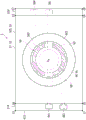
The following describes the variable wavelength interference filter 5 of the optical module 10. Fig. 3 is a plan view showing a schematic configuration of the variable wavelength interference filter 5.
As shown in fig. 2 and 3, the variable wavelength interference filter 5 is, for example, a rectangular plate-shaped optical component, and includes a fixed substrate 51 (first member) and a movable substrate 52 (second member). The fixed substrate 51 and the movable substrate 52 are formed of an insulating material such as various kinds of glass or quartz, and the fixed substrate 51 and the movable substrate 52 are integrally configured by bonding the fixed substrate 51 and the movable substrate 52 with a bonding film 53 (see fig. 2) made of, for example, a plasma polymerized film containing siloxane as a main component.
The fixed substrate 51 is provided with a fixed reflective film 54 which is one of the pair of reflective films constituting the present invention, and the movable substrate 52 is provided with a movable reflective film 55 which is the other of the pair of reflective films constituting the present invention. The fixed reflective film 54 and the movable reflective film 55 are disposed to face each other with a gap G1 (see fig. 2) therebetween.
The fixed substrate 51 is provided with a fixed electrode 561, and the movable substrate 52 is provided with a movable electrode 562. The fixed electrode 561 and the movable electrode 562 are disposed to face each other with a predetermined gap therebetween. These fixed electrode 561 and movable electrode 562 constitute an electrostatic actuator 56 as an example of the actuator of the present invention.
In the following description, a planar view of the variable wavelength interference filter 5 as viewed from the substrate thickness direction of the fixed substrate 51 or the movable substrate 52, that is, a planar view of the variable wavelength interference filter as viewed from the lamination direction of the fixed substrate 51, the bonding film 53, and the movable substrate 52 is a filter planar view. In the present embodiment, the center point of the fixed reflective film 54 and the center point of the movable reflective film 55 are aligned in a planar view of the filter, the center points of these reflective films in the planar view are referred to as filter center points O, and a straight line passing through the center points of these reflective films is referred to as a center axis.
(constitution of fixed substrate)
As shown in fig. 2, the fixed substrate 51 includes an electrode arrangement groove 511 and a reflective film installation portion 512 formed by etching or the like, for example. One end side (sides C1-C2 in fig. 3) of the fixed board 51 protrudes outward beyond the board end edge (sides C5-C6 in fig. 3) of the movable board 52, and constitutes a first terminal extraction portion 514.
The electrode arrangement groove 511 is formed in an annular shape with the filter center point O of the fixed substrate 51 as the center in a plan view of the filter. In a plan view of the filter, the reflective film providing portion 512 is formed to protrude from the center portion of the electrode arrangement groove 511 toward the movable substrate 52 side. A fixed electrode 561 of the electrostatic actuator 56 is provided on the bottom surface of the electrode arrangement groove 511. Further, a fixed reflective film 54 is provided on the projecting distal end surface of the reflective film providing section 512.
The fixed substrate 51 is provided with an electrode lead-out groove (not shown) extending from the electrode arrangement groove 511 to the outer peripheral edge of the fixed substrate 51.
The fixed electrode 561 is formed in an arc shape (substantially C-shaped), for example, and a C-shaped opening is provided in a portion near the side C1-C2 as shown in fig. 3. Further, an insulating film for securing insulation with the movable electrode 562 may be stacked on the fixed electrode 561.
The fixed electrode 561 includes a fixed extraction electrode 563 extending along the electrode extraction groove to the first terminal extraction portion 514. The extended tip of the fixed lead electrode 563 is connected to the voltage control unit 15 via, for example, an FPC (Flexible printed circuit) or a lead wire.
The fixed reflective film 54 provided on the protruding distal end surface of the reflective film providing section 512 is made of, for example, a metal film such as Ag or a reflective film material having conductivity such as Ag alloy. In addition, for example, TiO can also be used2As a high refractive layer, with SiO2A dielectric multilayer film as a low refractive layer is used as the fixed reflective film 54. When a dielectric multilayer film is used as the fixed reflective film 54, a conductive film is laminated on the lowermost layer or the uppermost layer (surface layer) of the dielectric multilayer film to impart conductivity. As the conductive film, a reflective film of Ag alloy or the like having high reflectance characteristics over a wide wavelength range can be used. In this case, the wavelength range to be measured of the variable wavelength interference filter 5 can be widened by the conductive film, a desired target wavelength can be extracted over a wide wavelength range, and light of the target wavelength can be extracted at high resolution by the dielectric multilayer film. Further, a transparent adhesive layer for improving adhesion may be further interposed between the conductive film and the reflective film providing portion 512 or between the conductive film and the dielectric multilayer film.
As shown in fig. 3, the fixed substrate 51 is provided with a first mirror electrode (ミラー computer) 541 connected to the outer peripheral edge of the fixed reflective film 54 and extending toward the first terminal extraction portion 514 through the C-shaped opening of the fixed electrode 561. The first mirror electrode 541 is formed by film formation simultaneously with the formation of the fixed reflection film 54.
The first mirror electrode 541 is connected to the voltage control unit 15 at the first terminal extraction unit 514.
The region of the fixed substrate 51 where the electrode arrangement groove 511, the reflective film setting section 512, and the electrode lead-out groove are not formed is bonded to the movable substrate 52 via the bonding film 53.
(constitution of Movable base plate)
In a plan view of the filter shown in fig. 3, the movable substrate 52 includes: a circular movable part 521 centered on the filter center point O, a holding part 522 coaxial with the movable part 521 and holding the movable part 521, and a substrate outer peripheral part 525 provided outside the holding part 522.
As shown in fig. 3, one end side (sides C7 to C8 in fig. 3) of the movable board 52 protrudes outward beyond the board end edge (sides C3 to C4 in fig. 3) of the fixed board 51, and constitutes the second terminal extraction portion 524.
The movable portion 521 is formed to be larger than the thickness of the holding portion 522, and for example, in the present embodiment, is formed to have the same thickness as the movable substrate 52. In a plan view of the filter, the movable portion 521 is formed to have a diameter larger than at least the diameter of the outer peripheral edge of the reflective film providing portion 512. A movable reflective film 55 and a movable electrode 562 are provided on a movable surface of the movable portion 521 facing the fixed substrate 51.
In a plan view of the filter, the movable electrode 562 is provided on the outer peripheral side of the movable reflective film 55, and is disposed to face the fixed electrode 561 with a gap therebetween. The movable electrode 562 is formed in an arc shape (substantially C-shaped), and as shown in fig. 3, a C-shaped opening is provided in a portion near the side C7-C8. In addition, a structure in which an insulating film is stacked on the movable electrode 562 may be employed as in the fixed electrode 561.
Here, as shown in fig. 3, in a plan view of the filter, the electrostatic actuator 56 is configured by an arc region (a region indicated by a right-upper hatched portion in fig. 3) where the movable electrode 562 and the fixed electrode 561 overlap. As shown in fig. 3, the electrostatic actuators 56 are disposed in a point-symmetrical shape with respect to the filter center point O in a plan view of the filter. Therefore, the electrostatic attraction generated when the voltage is applied to the electrostatic actuator 56 also acts on a position point-symmetric with respect to the filter center point O, and the movable portion 521 can be displaced toward the fixed substrate 51 with a balance maintained.
As shown in fig. 3, the movable electrode 562 is provided with a movable extraction electrode 564 extending toward the second terminal extraction portion 524. The movable extraction electrode 564 is disposed along a position facing an electrode extraction groove provided in the fixed substrate 51. The extended tip of the movable extraction electrode 564 is connected to the voltage control unit 15 through, for example, an FPC or a lead wire.
The movable reflective film 55 is provided so as to face the fixed reflective film 54 at the center of the movable surface of the movable portion 521 with an inter-reflective-film gap G1 interposed therebetween. As the movable reflective film 55, a reflective film having the same configuration as the fixed reflective film 54 described above is used. In the present embodiment, the gap G1 between the reflective films 54 and 55 is smaller than the gap between the electrodes 561 and 562.
As shown in fig. 3, the movable substrate 52 is provided with a second mirror electrode 551 connected to the outer peripheral edge of the movable reflective film 55 and extending toward the second terminal extraction portion 524 through the C-shaped opening of the movable electrode 562.
In the case where the movable reflective film 55 is formed of a laminate of a dielectric multilayer film and a conductive film, the second mirror electrode 551 is formed simultaneously with the conductive film and connected to the conductive film.
The second mirror electrode 551 is connected to the voltage control unit 15 at the second terminal extraction portion 524 through, for example, an FPC, a lead wire, or the like.
In the present embodiment, as shown in fig. 3, the gap G2 between the electrodes 561, 562 is larger than the gap G1, but the present invention is not limited thereto. For example, when infrared light is used as the measurement target light, the gap G1 may be larger than the gap G2 between the electrodes 561 and 562 depending on the wavelength range to be measured.
The holding portion 522 is a diaphragm that surrounds the periphery of the movable portion 521, and is formed smaller than the thickness of the movable portion 521. Such a holding portion 522 is more easily bent than the movable portion 521, and the movable portion 521 may be displaced toward the fixed board 51 by a slight electrostatic attraction. At this time, since the movable portion 521 has a larger thickness and a higher rigidity than the holding portion 522, even when the holding portion 522 is pulled toward the fixed substrate 51 by the electrostatic attraction, the shape change of the movable portion 521 can be suppressed. Therefore, the movable reflective film 55 provided in the movable portion 521 is also less likely to be bent, and the fixed reflective film 54 and the movable reflective film 55 can be always maintained in a parallel state.
In the present embodiment, the diaphragm-shaped holding portion 522 is exemplified, but the present invention is not limited to this, and for example, a configuration in which beam-shaped holding portions arranged at equal angular intervals are provided around the filter center point O, or the like, may be adopted.
As described above, the substrate outer peripheral portion 525 is provided outside the holding portion 522 in a filter plan view. The surface of the substrate outer peripheral portion 525 facing the fixed substrate 51 is bonded to the fixed substrate 51 via the bonding film 53.
[ constitution of Voltage control section ]
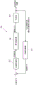
As shown in fig. 2, the voltage control unit 15 includes: a gap detector 151 (detection means in the present invention), a feedback control section 152, and a microcomputer (microcontroller) 16.
Fig. 4 is a conceptual diagram of a feedback loop using the voltage control unit 15.
As shown in fig. 4, the voltage control unit 15 forms a closed loop system (クローズドループシステム)15L (feedback loop) by the electrostatic actuator 56 of the variable wavelength interference filter 5, the gap detector 151, and the feedback control unit 152. In the present embodiment, the microcomputer 16 appropriately maintains the control state during the feedback control by setting the gain of the closed-loop system 15L based on the driving characteristics of the electrostatic actuator 56.
The configuration of the voltage control unit 15 will be described in detail below.
The gap detector 151 is connected to the first mirror electrode 541 and the second mirror electrode 551 of the variable wavelength interference filter 5. The gap detector 151 detects the size of the gap G1 between the reflective films 54 and 55, which varies due to the driving of the electrostatic actuator 56, and outputs a detection signal. Here, the driving amount of the electrostatic actuator 56 can be easily calculated by detecting the gap size of the gap G1, and the gap detector 151 functions as the detection means of the present invention.
Specifically, the gap detector 151 includes a C-V conversion circuit (not shown) and converts the capacitance between the reflective films 54 and 55 into a voltage value (detection signal). Examples of such a C-V conversion circuit include a switched capacitor circuit (スイッチト and キャパシタ circuits).
Then, the gap detector 151 outputs a detection signal to the feedback control section 152 and the microcomputer 16.
The gap detector 151 may output an analog signal as a detection signal or a digital signal as a detection signal. In the case of outputting a Digital signal, a detection signal (Analog signal) from the C-V conversion circuit is input to an ADC (Analog to Digital Converter) and converted into a Digital value.
The feedback control unit 152 corresponds to a controller of the present invention, and is connected to the fixed extraction electrode 563 and the movable extraction electrode 564 of the variable wavelength interference filter 5. The feedback control unit 152 applies a drive voltage to the electrostatic actuator 56 based on a command signal input from the microcomputer to set the gap G1 to a predetermined target value.
The feedback control unit 152 controls the increase and decrease of the drive voltage applied to the electrostatic actuator 56 so that the deviation between the detection signal from the gap detector 151 and the command signal input from the microcomputer 16 is equal to or less than a predetermined threshold value. That is, the feedback control unit 152 performs feedback control based on the detection signal and the command signal.
The feedback control section 152 can change the gain by the control of the microcomputer 16. The gain of the feedback control unit 152 is changed to adjust the gain of the entire closed loop system.
Specifically, when an analog controller is used as the feedback control unit 152, a gain setting circuit capable of setting any one of a plurality of gains is provided in the controller. Then, the gain of the gain setting circuit is set to a predetermined gain in accordance with a control signal from the microcomputer 16.
In the case of using a digital controller as the feedback control section 152, a parameter (register value) for controlling the gain is rewritten based on a signal from the microcomputer, and a predetermined gain can be set.
The microcomputer 16 includes a memory 161, and stores, for example, a relationship (gap-related data) between a detection signal (voltage signal) detected by the gap detector 151 and the size of the gap G1. Further, as the gap-related data, the size of the gap G2 with respect to the detection signal may be recorded.
In addition, the memory 161 stores therein drive characteristic data of the electrostatic actuator 56 indicating the size of the gap G2 (actuator gap) with respect to the drive voltage applied to the electrostatic actuator 56. In addition, the optimum gain is stored in association with each driving characteristic data.
Fig. 5 is a diagram showing an example of the driving characteristic data.
In the present embodiment, as shown in fig. 5, a plurality of pieces of drive characteristic data are recorded in which the size (initial gap size) of the gap G2 in the initial state where no drive voltage is applied to the electrostatic actuator 56 is different from each other.
As shown in fig. 2, the microcomputer 16 functions as a target command unit 162, a characteristic acquisition unit 163, and a gain setting unit 164.
When a wavelength setting command is input from the control unit 20, the target command unit 162 calculates the size (target value) of the gap G1 corresponding to the target wavelength, and outputs the calculated size (target value) as a target signal to the feedback control unit 152.
The characteristic acquisition unit 163 acquires the driving characteristics of the electrostatic actuator 56 based on the detection signal input from the gap detector 151.
Gain setting section 164 sets the gain of feedback control section 152 based on the driving characteristics acquired by characteristic acquisition section 163.
[ constitution of control section ]
Referring back to fig. 1, the control unit 20 of the spectrometry device 1 will be described.
The control unit 20 corresponds to a processing unit of the present invention, and is configured by combining a CPU, a memory, and the like, for example, and controls the overall operation of the spectrometry device 1. As shown in fig. 1, the control unit 20 includes a wavelength setting unit 21, a light amount obtaining unit 22, a spectroscopic measurement unit 23, and a storage unit 30.
Various programs for controlling the spectroscopic measurement apparatus 1 and various data (for example, V- λ data indicating a drive voltage for a target wavelength) are recorded in the storage unit 30.
The wavelength setting unit 21 sets a target wavelength of the light extracted by the variable wavelength interference filter 5, and outputs a control signal to the voltage control unit 15 to the effect that the set target wavelength is extracted from the variable wavelength interference filter 5.
The light quantity acquisition unit 22 acquires the light quantity of the light of the target wavelength transmitted through the variable wavelength interference filter 5 based on the light quantity acquired by the detector 11.
The spectroscopic measurement unit 23 measures the spectral characteristics of the measurement target light based on the light amount acquired by the light amount acquisition unit 22.
[ method for driving variable wavelength interference filter ]
Fig. 6 is a flowchart illustrating a method of driving the variable wavelength interference filter (actuator control method) in the spectroscopic measurement process of the spectroscopic measurement apparatus 1.
In order to obtain the intensity of light of each wavelength included in the measurement target light by the spectroscopic measurement apparatus 1, first, the control unit 20 sets the wavelength (target wavelength) of light transmitted through the variable wavelength interference filter 5 by the wavelength setting unit 21. The wavelength setting unit 21 outputs a wavelength setting command to the voltage control unit 15 so as to allow light of the set target wavelength to pass therethrough (step S1).
Next, the characteristic acquisition unit 163 of the microcomputer 16 acquires the driving characteristic data of the electrostatic actuator 56 based on the detection signal input from the gap detector 151 in the initial state (step S2).
Specifically, the characteristic acquisition unit 163 acquires the initial gap size of the gap G1 between the reflective films 54 and 55 based on the detection signal input from the gap detector 151, and calculates the initial value (initial gap size) of the gap G2 between the electrodes 561 and 562 based on the initial gap of the gap G1. Then, the characteristic acquisition unit 163 acquires the drive characteristic data corresponding to the calculated initial gap size of the gap G2 from the plurality of drive characteristic data stored in the memory.
Next, gain setting section 164 obtains an optimum gain for the obtained drive characteristic data (step S3).
In the present embodiment, the optimum gain associated with each drive characteristic data is read.
Further, although an example in which the gain is associated with the drive characteristic data is shown, for example, table data showing a relationship of the gain with respect to the initial gap size of the gap G2 may be stored in advance in the memory 161.
When a reference gain is set with respect to the drive characteristic data (reference characteristic data) serving as a reference, gain setting section 164 may perform processing such as calculation of a gain based on the drive characteristic data acquired in step S2 and the reference characteristic data.
For example, in fig. 5, when the drive characteristic data of curve a is set as the reference data and the reference gain Gc is set for the reference data, and the drive characteristic data of curve B is acquired in step S2, gain setting section 164 calculates the sensitivity ratio of each drive characteristic data.
For example, in the reference data of the curve a, when the actuator gap G2 is set to G α, the sensitivity in the feedback control is R α (m/V), the drive characteristic changes to the curve B, and the sensitivity in the feedback control when the gap G2 is set to G α changes to R β (m/V). At this time, gain setting section 164 sets a gain that is (R β/R α) times reference gain Gc. This suppresses a sensitivity change during feedback control, and suppresses a problem such as abnormal oscillation or an increase in the setting time to the target value.
Then, gain setting section 164 outputs a control signal for setting the gain acquired in step S3 to feedback control section 152 and sets the gain (step S4).
Then, the target command unit 162 outputs a target signal indicating a target value of the gap G2 of the electrostatic actuator 56 to the feedback control unit 152 based on the target wavelength included in the wavelength setting command input in step S1. Thereby, the feedback control unit 152 performs feedback control (step S5).
That is, the feedback control unit 152 controls the drive voltage applied to the electrostatic actuator 56 so that the deviation between the detection signal input from the gap detector 151 and the target signal approaches 0.
In step S5, the size of the gap G1 of the variable wavelength interference filter 5 is set to a size corresponding to the target wavelength set in step S1, and light centered on the target wavelength is emitted from the variable wavelength interference filter 5. Thus, the detector 11 receives the light of the target wavelength, and the light quantity acquisition unit 22 of the control unit 20 acquires the light quantity of the light of the target wavelength based on the light quantity detection signal input from the detector 11 (step S6).
[ Effect of the first embodiment ]
In the present embodiment, characteristic acquisition section 163 measures the driving characteristics of electrostatic actuator 56 based on the detection signal from gap detector 151, and gain setting section 164 sets the gain in feedback control corresponding to the measured driving characteristics.
Therefore, even if the driving characteristics of the electrostatic actuator 56 fluctuate due to, for example, environmental changes, aging, or the like, an optimum gain corresponding to the fluctuating driving characteristics can be set. This makes it possible to avoid a problem that the electrostatic actuator 56 abnormally oscillates and an excessive time is required to output light of a target wavelength during feedback control, and thus, optimal feedback control can be performed.
By performing such optimal feedback control, the light amount of light of the target wavelength can be acquired more quickly in the optical module 10, and the spectroscopic measurement process in the spectroscopic measurement device 1 can be performed more quickly.
In the present embodiment, the characteristic acquisition unit 163 acquires the initial gap size of the gap G2 in the initial state where the driving voltage is not applied to the electrostatic actuator 56, and reads the driving characteristic data corresponding to the initial gap size.
The behavior characteristic (the behavior can be predicted from the initial gap size of the gap G2, for example, when the spring constant of the holding portion 522 of the variable wavelength interference filter 5 is assumed to be constant. Further, as in the present embodiment, by storing a plurality of pieces of drive characteristic data in advance in the memory 161, it is possible to acquire the drive characteristic data with respect to the initial gap size more quickly. This makes it possible to more quickly set the gain and to more quickly start the feedback control.
[ second embodiment ]
Next, a second embodiment of the present invention will be described with reference to the drawings.
In the first embodiment described above, in step S2, the characteristic acquisition unit 163 acquires the driving characteristics of the electrostatic actuator 56 according to the initial gap size of the gap G2. In contrast, the second embodiment is different from the first embodiment in that the driving characteristics of the electrostatic actuator 56 are acquired based on a plurality of measurement points.
In the following description, the same reference numerals are used for the components already described, and the description thereof will be omitted or simplified.
Fig. 7 is a diagram for explaining a method of acquiring drive characteristic data according to the second embodiment.
In the present embodiment, in step S2, the characteristic acquisition unit 163 acquires the size (measurement point c) of the gap G2 based on the detection signal from the gap detector when the driving voltage is applied, with respect to the driving voltage applied to the electrostatic actuator 56, by changing the driving voltage.
Then, based on these acquired measurement points C, characteristic acquisition section 163 acquires curve data C of the driving characteristics by, for example, polynomial approximation or the like.
In the present embodiment, the drive characteristic data based on the plurality of measurement points c is obtained. In this case, for example, it is possible to measure the change in the driving characteristics based on more parameters such as the spring constant of the holding portion 522 of the variable wavelength interference filter 5. By obtaining the drive characteristic data corresponding to such a large change in the parameter, the control gain in the feedback control of the electrostatic actuator 56 can be set more accurately, and stable feedback control can be performed.
[ third embodiment ]
Next, a third embodiment of the present invention will be described with reference to the drawings.
In the first and second embodiments, the optical module 10 in which the gap G1 between the reflective films 54 and 55 is controlled to a desired value by one electrostatic actuator 56 is exemplified.
In contrast, the third embodiment is different from the first and second embodiments in that the electrostatic actuator includes a first actuator and a second actuator that can be independently driven, and the size of the gap G1 is controlled by the first and second actuators.
Fig. 8 is a diagram showing a schematic configuration of an optical module according to a third embodiment. Fig. 9 is a top view of a variable wavelength interference filter.
[ constitution of variable wavelength interference Filter ]
The variable wavelength interference filter 5A of the present embodiment is different in electrode configuration from the first and second embodiments. In the variable wavelength interference filter 5A of the present embodiment, electrodes having a double electrode structure are provided outside the reflective films 54 and 55 in a filter plan view.
Specifically, as shown in fig. 8 and 9, the electrostatic actuator of the variable wavelength interference filter 5A according to the present embodiment is composed of a first electrostatic actuator 56A and a second electrostatic actuator 56B.
The first electrostatic actuator 56A includes a first fixed electrode 561A provided on the fixed substrate 51 and a first movable electrode 562A provided on the movable substrate 52.
The first fixed extraction electrode 563A is connected to the first fixed electrode 561A, the first movable extraction electrode 564A is connected to the first movable electrode 562A, and these extraction electrodes 563A and 564A are connected to the voltage control unit 15A, respectively.
The second electrostatic actuator 56B is provided outside the first electrostatic actuator 56A, and includes a second fixed electrode 561B provided on the fixed substrate 51 and a second movable electrode 562B provided on the movable substrate 52.
The second fixed extraction electrode 563B is connected to the second fixed electrode 561B, the second movable extraction electrode 564B is connected to the second movable electrode 562B, and these extraction electrodes 563B and 564B are connected to the voltage control unit 15A.
[ constitution of Voltage control section ]
Fig. 10 is a conceptual diagram of a feedback loop (closed loop system) according to the present embodiment.
In the closed loop system 15L of the voltage control unit 15A of the present embodiment, a bias driving unit 153 (bias voltage applying means of the present invention) is further provided to the voltage control unit 15 of the first embodiment.
The lead electrodes 563A and 564A of the first electrostatic actuator 56A are connected to the bias driving unit 153.
The extraction electrodes 563B and 564B of the second electrostatic actuator 56B are connected to the feedback control unit 152A.
The bias driving section 153 applies a bias voltage to the first electrostatic actuator 56A. Specifically, the bias driving section 153 applies a voltage to the first electrostatic actuator 56A based on a bias signal input from the microcomputer 16A.
The feedback control unit 152 applies a feedback voltage to the second electrostatic actuator 56B. At this time, the feedback control unit 152 applies a feedback voltage to the second electrostatic actuator 56B so that the detection signal input from the gap detector 151 and the target signal input from the microcomputer 16A have the same value.
In the present embodiment, the gain of the feedback control unit 152 is a fixed gain and is kept constant.
The microcomputer 16A has a memory 161, and records gap-related data, drive characteristic data, set gains corresponding to the respective drive characteristic data, and the like, as in the first embodiment.
The microcomputer 16A functions as a target instruction unit 162, a characteristic acquisition unit 163, and a bias instruction unit 165.
The bias instruction unit 165 outputs a bias instruction instructing to apply a bias voltage to the bias driving unit 153 based on the wavelength setting instruction input from the control unit 20.
[ method for driving variable wavelength interference filter ]
Fig. 11 is a flowchart illustrating a driving method (actuator control method) of the variable wavelength interference filter.
In order to obtain the intensity of light of each wavelength included in the light to be measured by the spectroscopic measurement apparatus 1, first, as in the first embodiment, a wavelength setting command is output from the control unit 20 to the voltage control unit 15 by the processing of step S1. When the microcomputer 16A receives the wavelength setting command, it calculates a target value (target signal) of the gap G1 corresponding to the target wavelength.
Then, similarly to step S2, the characteristic acquisition unit 163 acquires the detection signal input from the gap detector 151 in the initial state, and acquires the initial gap size of the gap G1 between the reflective films 54 and 55. In addition, similarly to the second embodiment, a plurality of measurement points c may be obtained to obtain the driving characteristics. In this case, the size of the gap G2 when the bias voltage is applied from the bias driving unit 153 is obtained as the measurement point c.
Next, the bias instruction unit 165 acquires the optimum bias voltage corresponding to the acquired drive characteristic data (step S11).
Specifically, the bias voltage command unit 165 calculates a bias voltage corresponding to the target value of the gap G1.
That is, in the present embodiment, in the feedback control, the bias voltage is set so that the sensitivity (sensitivity) (gap displacement amount (m/V) with respect to the applied voltage) when the voltage is applied to the second electrostatic actuator 56B is constant.
Here, the sensitivity R when a voltage is applied to the second electrostatic actuator 56BC(m/V) is represented by the following formula (1).
[ mathematical formula 1]

In formula (1), VbIs a bias voltage applied to the first electrostatic actuator 56A, k is a spring coefficient of the movable substrate 52 (holding part 522), ε is a dielectric constant between the fixed substrate 51 and the movable substrate 52 (inter-electrode gap G2), and S isbIs the effective area of the first electrostatic actuator 56A (the area of the region where the first fixed electrode 561A and the first movable electrode 562A overlap in a filter plan view), SCIs the effective area of the second electrostatic actuator 56B, dmaxThe initial gap amount of the inter-electrode gap G2 is d, and the target displacement amount of the movable part 521 (gap displacement amount of the inter-electrode gap G2) is d, which allows light of the target wavelength to pass through.
In the present embodiment, during the feedback control, the bias voltage V is applied so that the sensitivity when the voltage is applied to the second electrostatic actuator 56B is constantb. That is, in the above formula (1), VCIs a fixed value, and is preset in accordance with a fixed gain in a controller constituting the feedback control section 152AThe value is obtained. Further, if a wavelength setting command for specifying a target wavelength is input from the control unit 20, the microcomputer 16A can calculate a target value of the gap G1 necessary for extracting light of the target wavelength from the variable wavelength interference filter 5A, and can calculate an amount (target displacement amount d) by which the movable unit 521 should be displaced from the target value.
In the above formula (1), for VbSolving, the following equation (2) can be derived.
[ mathematical formula 2]

The bias command unit 165 calculates a bias voltage having a constant sensitivity when a voltage is applied to the second electrostatic actuator 56B based on the above equation (2), and outputs a bias command to the bias driving unit 153, the bias command being intended to apply the bias voltage to the first electrostatic actuator 56A. Thereby, a bias voltage is applied from the bias driving portion 153 to the first electrostatic actuator 56A (step S12).
That is, in the present embodiment, by fixing the gain of the feedback control unit 152 and setting the optimum bias voltage corresponding to the driving characteristics of the electrostatic actuator 56 by the bias command means 165, the sensitivity of the second electrostatic actuator 56B at the time of voltage application is adjusted, and the gain in the entire closed loop system 15L is optimized. Therefore, in the present embodiment, the bias instruction means 165 functions as gain setting means in the present invention.
Then, the feedback control of step S5 and the light amount acquisition of step S6 are performed.
In the present embodiment, the electrostatic actuator 56 is configured by a first electrostatic actuator 56A to which a bias voltage is applied by the bias driving unit 153, and a second electrostatic actuator 56B to which a feedback voltage is applied by the feedback control unit 152A. Then, the bias instruction unit 165 resets the bias voltage in the bias driving section 153 based on the driving characteristics of the electrostatic actuator 56 acquired by the characteristic acquisition unit 163.
Therefore, in the present embodiment, as in the above-described embodiment, even when the drive characteristic of the actuator fluctuates, the bias voltage of the bias drive unit can be set to an optimum value according to the fluctuating characteristic, and the gain in the entire closed-loop system 15L can be controlled so that the sensitivity in the feedback control of the second electrostatic actuator 56B becomes constant. Thereby, an optimum feedback control can be performed.
[ other embodiments ]
The present invention is not limited to the above-described embodiments, and modifications, improvements, and the like within a range that can achieve the object of the present invention are included in the present invention.
For example, in the present invention, an electrostatic actuator that changes the size of the gap G1 in the variable wavelength interference filters 5 and 5A is exemplified as the actuator, but the present invention is not limited to this. For example, other actuators such as a piezoelectric actuator and an induction coil actuator may be used as the feedback loop of the actuator. In particular, in the case of an actuator in which the drive amount varies nonlinearly with respect to the drive voltage, if the optimum gain is not set in the feedback control due to the variation of the drive characteristic, there is a possibility that the normal drive is disturbed by the abnormal oscillation or the like as described above. The present invention is effective for such an actuator in which the drive characteristic varies nonlinearly, and can perform feedback control in which an optimum control state is maintained by setting an optimum gain.
In the above embodiment, the reflective films 54 and 55 are used as electrodes for capacitance detection, but the present invention is not limited thereto. For example, the capacitance detection electrodes may be provided on the fixed substrate 51 and the movable substrate 52 separately from the reflective films 54 and 55 so as to face each other.
In addition, the reflective films 54 and 55 may be used as driving electrodes. For example, in the third embodiment, the reflective films 54 and 55 may function as the second electrostatic actuator or the first electrostatic actuator.
The driving amount detection means is not limited to the configuration using the above-described capacitance detection electrode, and may be, for example, a configuration in which the bending state of the movable substrate 52 (holding portion 522) is detected by a strain gauge or the like to detect the gap amount of the inter-reflective-film gap G1, or a configuration in which an optical sensor for detecting the gap amount is provided outside.
In each of the above embodiments, the bias voltage applied to the bias driving unit 153 is set based on the formula (2), but the present invention is not limited to this. For example, a configuration may be adopted in which the bias voltage with respect to the target value of the gap G1 between the reflective films 54 and 55 is stored as table data and stored in the storage unit. In this case, the microcomputer 16 may read the offset voltage with respect to the target gap amount from the table data without performing calculation of the offset voltage based on the equation (2).
Further, as the bias voltage, a voltage smaller than a drive voltage for setting the inter-reflective film gap G1 to a target gap amount by driving the bias drive unit 153 alone may be used. By applying such a bias voltage, the sensitivity can be reduced and the accuracy of the feedback control can be improved in comparison with the case where no bias voltage is applied in the control of the second electrostatic actuator 56B by the feedback control section 152.
In the third embodiment, the example in which the first electrostatic actuator 56A to which the bias voltage is applied is disposed on the outer peripheral side of the second electrostatic actuator 56B to which the feedback voltage is applied is shown, but the present invention is not limited thereto. For example, the first electrostatic actuator 56A may be provided on the outer periphery of the reflective films 54 and 55 and on the inner periphery of the second electrostatic actuator 56B, and the second electrostatic actuator 56B may be provided on the outer periphery of the first electrostatic actuator 56A.
In addition, as the electronic device of the present invention, the spectroscopic measuring apparatus 1 is exemplified in the above embodiments, and the method for driving the variable wavelength interference filter, the optical module, and the electronic device of the present invention can be applied to various fields.
For example, as shown in fig. 12, the electronic device of the present invention may be used as a color measuring device for measuring a color.
Fig. 12 is a block diagram showing an example of a colorimeter device 400 provided with a variable wavelength interference filter.
As shown in fig. 12, the color measuring apparatus 400 includes: a light source device 410 for emitting light to the inspection object a, a colorimetric sensor 420 (optical module), and a control device 430 (processing unit) for controlling the overall operation of the colorimetric device 400. The colorimetric device 400 is a device that reflects the light emitted from the light source device 410 to the inspection object a, receives the reflected inspection object light by the colorimetric sensor 420, and analyzes and measures the chromaticity of the measurement object light, that is, the color of the inspection object a, based on a detection signal output from the colorimetric sensor 420.
The light source device 410 includes a light source 411 and a plurality of lenses 412 (only 1 is shown in fig. 12), and emits reference light (e.g., white light) to the inspection object a, for example. In this case, the light source device 410 converts the reference light emitted from the light source 411 into parallel light by the collimator lens, and emits the parallel light toward the inspection object a from a projection lens not shown. Although the colorimeter 400 including the light source device 410 is illustrated in the present embodiment, the light source device 410 may not be provided when the inspection object a is a light-emitting member such as a liquid crystal panel, for example.
As shown in fig. 12, the colorimetric sensor 420 includes: a variable wavelength interference filter 5; a detector 11 that receives the light transmitted through the wavelength variable interference filter 5; and a voltage control unit 15 for varying the wavelength of the light transmitted through the variable wavelength interference filter 5. The colorimetric sensor 420 includes an incident optical lens (not shown) for guiding the reflected light (inspection target light) reflected by the inspection target a to the inside at a position facing the variable wavelength interference filter 5. The colorimetric sensor 420 splits the light of a predetermined wavelength out of the inspection target light incident from the incident optical lens by the variable wavelength interference filter 5, and receives the split light by the detector 11. Instead of the variable wavelength interference filter 5, a variable wavelength interference filter 5A may be disposed.
The control device 430 controls the overall operation of the color measuring device 400.
As the control device 430, for example, a general-purpose personal computer, a portable information terminal, another dedicated color measurement computer, or the like can be used. As shown in fig. 12, the control device 430 includes a light source control unit 431, a colorimetric sensor control unit 432, a colorimetric processing unit 433, and the like.
The light source control unit 431 is connected to the light source device 410, and outputs a predetermined control signal to the light source device 410 based on a setting input by a user, for example, to emit white light of a predetermined luminance.
The colorimetric sensor control unit 432 is connected to the colorimetric sensor 420, sets the wavelength of light received by the colorimetric sensor 420 based on a setting input by a user, for example, and outputs a control signal for detecting the amount of light received at the wavelength to the colorimetric sensor 420. Thus, the voltage control unit 15 of the colorimetric sensor 420 applies a voltage to the electrostatic actuator 56 based on the control signal, and drives the variable wavelength interference filter 5.
The colorimetric processing unit 433 analyzes the chromaticity of the inspection object a from the amount of received light detected by the detector 11.
In addition, as another example of the electronic device of the present invention, a light-based system that detects the presence of a specific substance may be cited. As such a system, for example, there can be illustrated: a gas detection device such as a vehicle-mounted gas leak detector and a photoacoustic inert gas detector for a respiratory inspection, which detects a specific gas with high sensitivity by using a spectroscopic measurement method using a wavelength variable interference filter according to the present invention.
An example of such a gas detection device will be described below with reference to the drawings.
Fig. 13 is a schematic diagram showing an example of a gas detection device provided with a variable wavelength interference filter.
Fig. 14 is a block diagram showing the configuration of a control system of the gas detection device shown in fig. 13.
As shown in fig. 13, the gas detection device 100 includes a sensor chip 110, a flow path 120, and a main body 130, and the flow path 120 includes: a suction port 120A, a suction channel 120B, a discharge channel 120C, and a discharge port 120D.
The main body 130 includes a sensor cover 131 having an opening for detachably attaching the flow path 120, a discharge unit 133, a case 134, an optical unit 135, an optical filter 136, a variable wavelength interference filter 5, a detection device (optical module) such as a light receiving element 137 (detection unit), a control unit 138 (processing unit), a power supply unit 139, and the like, the control unit 138 processes a detected signal and controls the detection unit, and the power supply unit 139 supplies power. The optical unit 135 includes a light source 135A for emitting light, a beam splitter 135B, and lenses 135C, 135D, and 135E, and the beam splitter 135B reflects the light incident from the light source 135A toward the sensor chip 110 and transmits the light incident from the sensor chip to the light receiving element 137.
As shown in fig. 14, an operation panel 140, a display unit 141, a connection unit 142 for interfacing with the outside, and a power supply unit 139 are provided on the surface of the gas detection device 100. When the power supply unit 139 is a secondary battery, a connection unit 143 for charging may be provided.
As shown in fig. 14, the control unit 138 of the gas detection apparatus 100 includes: a signal processing unit 144 including a CPU or the like, a light source driver circuit 145 for controlling the light source 135A, a voltage control unit 146 for controlling the variable wavelength interference filter 5, a light receiving circuit 147 for receiving a signal from the light receiving element 137, a sensor chip detection circuit 149 for receiving a signal from the sensor chip detector 148, a discharge driver circuit 150 for controlling the discharge unit 133, and the like, wherein the sensor chip detector 148 reads a code of the sensor chip 110 to detect the presence or absence of the sensor chip 110.
Next, the operation of the gas detection apparatus 100 described above will be described.
A sensor chip detector 148 is provided inside the sensor section cover 131 on the upper portion of the main body section 130, and the presence or absence of the sensor chip 110 is detected by the sensor chip detector 148. When detecting the detection signal from the sensor chip detector 148, the signal processing unit 144 determines that the sensor chip 110 is mounted, and outputs an indication signal indicating that the detection operation can be performed to the display unit 141.
When the user operates the operation panel 140 and outputs an instruction signal for starting the detection process from the operation panel 140 to the signal processing unit 144, for example, the signal processing unit 144 outputs a signal for operating the light source to the light source driver circuit 145 to operate the light source 135A. When the light source 135A is driven, a stable laser beam of linearly polarized light is emitted from the light source 135A at a single wavelength. The light source 135A incorporates a temperature sensor and a light amount sensor, and outputs information thereof to the signal processing unit 144. When determining that the light source 135A is operating stably based on the temperature and the amount of light input from the light source 135A, the signal processing unit 144 controls the discharge driver circuit 150 to operate the discharge unit 133. Thereby, the gas sample containing the target substance (gas molecule) to be detected is guided from the suction port 120A to the suction channel 120B, the sensor chip 110, the discharge channel 120C, and the discharge port 120D. Further, a dust removal filter 120A1 for removing relatively large dust, a part of water vapor, and the like is provided at the suction port 120A.
The sensor chip 110 is a sensor in which a plurality of metal nanostructures are assembled and local surface plasmon resonance is utilized. In such a sensor chip 110, an enhanced electric field is formed between the metal nanostructures by laser light, and if gas molecules enter the enhanced electric field, raman scattered light and rayleigh scattered light containing information on molecular vibration are generated.
The rayleigh scattered light and the raman scattered light are incident on the optical filter 136 through the optical unit 135, the rayleigh scattered light is separated by the optical filter 136, and the raman scattered light is incident on the variable wavelength interference filter 5. Then, the signal processing section 144 outputs a control signal to the voltage control section 146. Thus, the voltage control unit 146 is configured by the gap detector 151, the feedback control unit 152, and the microcomputer 16 as in the first embodiment, and drives the variable wavelength interference filter 5 by the same driving method as in the first embodiment, and disperses the raman scattered light corresponding to the gas molecules to be detected by the variable wavelength interference filter 5. The same configuration as that of the voltage control unit 15A according to the third embodiment may be adopted.
After that, when the dispersed light is received by the light receiving element 137, a light receiving signal corresponding to the light receiving amount is output to the signal processing unit 144 via the light receiving circuit 147. In this case, the target raman scattered light can be extracted from the variable wavelength interference filter 5 with high accuracy.
The signal processing unit 144 compares the spectrum data of the raman scattered light corresponding to the gas molecule to be detected obtained as described above with the data stored in the ROM, determines whether or not the target gas molecule is present, and specifies the substance. The signal processing unit 144 causes the display unit 141 to display the result information thereof, or outputs the result information to the outside from the connection unit 142.
Although the gas detection apparatus 100 for detecting a gas by splitting the raman scattered light by the variable wavelength interference filter 5 and detecting the gas from the split raman scattered light is illustrated in fig. 13 and 14, the gas detection apparatus may be used as a gas detection apparatus for specifying a gas type by detecting the absorbance inherent in the gas. In this case, the optical module of the present invention is used as a gas sensor that flows a gas into the sensor to detect light absorbed by the gas in incident light. The electronic device of the present invention is a gas detection device that analyzes and determines the gas flowing into the sensor by the gas sensor. In such a configuration, the components of the gas may be detected using a variable wavelength interference filter.
The system for detecting the presence of a specific substance is not limited to the detection of the gas, and a substance component analyzer such as a non-invasive measuring device for measuring saccharides by near infrared spectroscopy, or a non-invasive measuring device for measuring information such as food, living body, and mineral can be exemplified.
Next, a food analysis device will be described as an example of the above-described substance component analysis device.
Fig. 15 is a diagram showing a schematic configuration of a food analysis apparatus as an example of an electronic device using the variable wavelength interference filter 5.
As shown in fig. 15, the food analysis device 200 includes a detector 210 (optical module), a control unit 220, and a display unit 230. The detector 210 includes a light source 211 that emits light, an imaging lens 212 into which light from the measurement object is introduced, a variable wavelength interference filter 5 that disperses the light introduced from the imaging lens 212, and an imaging unit 213 (detection unit) that detects the dispersed light.
Further, the control unit 220 includes: a light source control unit 221 for performing lighting/lighting-off control of the light source 211 and brightness control during lighting; a voltage control unit 222 for controlling the variable wavelength interference filter 5; a detection control unit 223 for controlling the imaging unit 213 to acquire the spectral image captured by the imaging unit 213; a signal processing unit 224 (analysis unit); and a storage section 225.
In the food analysis device 200, when the system is driven, the light source 211 is controlled by the light source control unit 221, and the measurement object is irradiated with light from the light source 211. Then, the light reflected by the object to be measured is incident on the variable wavelength interference filter 5 through the imaging lens 212. The variable wavelength interference filter 5 is driven by the driving method described in the first embodiment by the control of the voltage control unit 222. This enables light of the target wavelength to be extracted from the variable wavelength interference filter 5 with high accuracy. The extracted light is then captured by an imaging unit 213, which is configured by a CCD camera or the like, for example. The captured light is stored in the storage unit 225 as a spectral image. The signal processing unit 224 controls the voltage control unit 222 to change the voltage value applied to the variable wavelength interference filter 5, thereby acquiring a spectral image corresponding to each wavelength.
Then, the signal processing unit 224 performs arithmetic processing on the data of each pixel in each image stored in the storage unit 225 to obtain a spectrum at each pixel. Further, the storage unit 225 stores information on the components of the food with respect to the spectrum, for example, and the signal processing unit 224 analyzes the data of the obtained spectrum based on the information on the food stored in the storage unit 225 to obtain the food components and the contents thereof included in the detection target. Further, the calorie, freshness and the like of the food can be calculated from the obtained food components and contents. Further, by analyzing the spectral distribution in the image, it is possible to extract a portion of the food to be inspected where freshness is reduced, and to detect foreign matter and the like contained in the food.
The signal processing unit 224 performs processing for causing the display unit 230 to display information such as the composition, content, calorie, and freshness of the food to be examined, which is obtained as described above.
Although fig. 15 shows an example of the food analyzer 200, the food analyzer may be used as a non-invasive measuring device for other information as described above, based on a substantially similar configuration. For example, the present invention can be used as a biological analyzer for analyzing a biological component, such as measurement and analysis of a liquid component such as blood. As such a bioanalyzer, for example, if an apparatus for detecting alcohol is used as an apparatus for measuring a body fluid component such as blood, it can be used as a drunk driving prevention apparatus for detecting a drunk state of a driver. In addition, the present invention can also be used as an electronic endoscope system including such a biological analyzer.
Further, the present invention can be used as a mineral analysis device for performing a component analysis of a mineral.
The variable wavelength interference filter, the optical module, and the electronic device according to the present invention can be applied to the following devices.
For example, in the case where data can be transmitted by light of each wavelength by changing the intensity of light of each wavelength with time, data transmitted by light of a specific wavelength can be extracted by splitting light of a specific wavelength by a variable wavelength interference filter provided in an optical module and receiving the light by a light receiving unit, and optical communication can be performed by processing data of light of each wavelength by an electronic device including such an optical module for data extraction.
Further, the present invention can be applied to a spectral camera, a spectral analyzer, and the like that capture a spectral image by splitting light with the variable wavelength interference filter of the present invention. An example of such a spectral camera is an infrared camera incorporating a variable wavelength interference filter.
Fig. 16 is a schematic diagram showing a schematic configuration of the spectroscopic camera. As shown in fig. 16, the spectroscopic camera 300 includes a camera main body 310, an imaging lens unit 320, and an imaging unit 330 (detection unit).
The camera body 310 is a part that is held and operated by a user.
The imaging lens unit 320 is provided in the camera body 310, and guides the incident image light to the imaging unit 330. As shown in fig. 16, the imaging lens unit 320 includes an objective lens 321, an imaging lens 322, and a variable wavelength interference filter 5 provided between these lenses.
The imaging unit 330 is composed of a light receiving element and captures image light guided by the imaging lens unit 320.
In the spectral camera 300, light of a wavelength to be imaged is transmitted through the variable wavelength interference filter 5, and a spectral image of light of a desired wavelength can be imaged. At this time, the voltage control unit (not shown) drives the variable wavelength interference filter 5 for each wavelength by the driving method of the present invention shown in the first embodiment described above, and can accurately extract the image light of the spectral image of the target wavelength.
The variable wavelength interference filter of the present invention may be used as a bandpass filter, and for example, may be used as an optical laser device that transmits only light in a narrow band (narrow band) centered on a predetermined wavelength among light in a predetermined wavelength range emitted from the light emitting element by the variable wavelength interference filter.
The variable wavelength interference filter of the present invention can be used as a biometric authentication device, and can be applied to an authentication device using light in the near infrared region or visible region, blood vessels, fingerprints, retina, iris, and the like.
Further, the optical module and the electronic device may be used as the concentration detection apparatus. In this case, infrared energy (infrared light) emitted from the substance is split by the variable wavelength interference filter and analyzed, and the concentration of the sample in the sample is measured.
As described above, the variable wavelength interference filter, the optical module, and the electronic device according to the present invention can be applied to any device that splits predetermined light from incident light. Further, as described above, the variable wavelength interference filter of the present invention can perform the spectral measurement of a spectrum of a plurality of wavelengths and the detection of a plurality of components with high accuracy because a plurality of wavelengths can be separated by one device. Therefore, the optical module and the electronic device can be more miniaturized than the conventional device in which a desired wavelength is extracted by a plurality of devices, and can be suitably used as an optical device for portable use and vehicle-mounted use, for example.
Further, in the above-described embodiment, an example is described in which the driving characteristics are acquired from the gap size of the electrostatic actuator 56 provided between the substrates, and the gain in the feedback control of the electrostatic actuator 56 is set, but the present invention is not limited thereto.
For example, the present invention can be used for feedback control of an actuator driving device in which a driving amount changes non-linearly with respect to a driving voltage by applying a voltage, and examples of such an actuator include a piezoelectric actuator (ピエゾアクチュエーター). Specifically, the present invention is also applicable to a mirror device (ミラー デ バ イ ス) and the like in which the mirror plate is changed in posture by an angle corresponding to a driving voltage by applying the driving voltage to a piezoelectric actuator. In this case, a configuration may be employed in which the drive characteristics of the piezoelectric actuator are obtained by detecting the drive amount (drive angle, etc.) of the piezoelectric actuator when a predetermined drive voltage is applied, and the drive of the piezoelectric actuator is feedback-controlled based on the obtained drive characteristics.
In addition, the specific structure in carrying out the present invention may be changed to another structure or the like as appropriate within the range to achieve the object of the present invention.
Claims (8)
1. An actuator control device, characterized by comprising:
a detection unit that detects a gap size between a first reflective film of a variable wavelength interference filter and a second reflective film of the variable wavelength interference filter; and
a feedback loop controlling a driving voltage applied to an actuator of the variable wavelength interference filter according to the detected gap size,
setting a gain in the feedback loop according to a driving characteristic of the actuator based on the detected gap size,
the actuator control device further includes a gain setting unit that sets the gain,
the gain setting means acquires a plurality of combinations of the drive voltage and the gap size detected by the detection means when the drive voltage is applied, and sets the gain based on the combinations.
2. The actuator control device according to claim 1,
the actuator control device is provided with a first member and a second member opposite to the first member,
the actuator includes a first electrode provided on the first member and a second electrode provided on the second member and opposed to the first electrode,
the detection unit detects a gap size between the first member and the second member.
3. The actuator control device according to claim 1,
the feedback loop has a controller that controls the drive voltage based on the gap size detected by the detection unit and a target value of the gap size,
the gain setting unit sets a gain of the controller.
4. The actuator control device according to claim 1,
the feedback loop is provided with: a bias voltage applying unit that applies a predetermined bias voltage to the first actuator; and a controller that controls a drive voltage applied to a second actuator based on the gap size detected by the detection unit and a target value of the gap size,
the gain setting unit sets the bias voltage in the bias voltage applying unit.
5. An optical module is provided with:
the actuator control device of any one of claims 1 to 4.
6. An electronic device is characterized by comprising:
the actuator control device of any one of claims 1 to 4; and
the processing unit performs a predetermined process.
7. An actuator control method, characterized by comprising:
detecting a size of a gap between a first reflective film of a variable wavelength interference filter and a second reflective film of the variable wavelength interference filter;
obtaining a driving characteristic of an actuator of the variable wavelength interference filter based on the detected gap size; and
setting a gain in a feedback loop that controls a drive voltage applied to the actuator according to the detected gap size based on the drive characteristic,
a plurality of combinations of the drive voltage and the gap size detected when the drive voltage is applied are obtained, and the gain is set based on the combinations.
8. An actuator control device, characterized by comprising:
a detection unit that detects a gap size between a first reflective film of a variable wavelength interference filter and a second reflective film of the variable wavelength interference filter; and
a feedback control unit for controlling a drive voltage applied to the actuator of the variable wavelength interference filter based on the detected gap size,
setting a gain in the feedback control section in accordance with a driving characteristic of the actuator based on the detected gap size,
the actuator control device further includes a gain setting unit that sets the gain,
the gain setting means acquires a plurality of combinations of the drive voltage and the gap size detected by the detection means when the drive voltage is applied, and sets the gain based on the combinations.
Applications Claiming Priority (3)
| Application Number | Priority Date | Filing Date | Title |
|---|---|---|---|
| JP2014012125A JP6543884B2 (en) | 2014-01-27 | 2014-01-27 | Actuator control device, optical module, electronic device, and actuator control method |
| JP2014-012125 | 2014-01-27 | ||
| CN201510038264.0A CN104808333A (en) | 2014-01-27 | 2015-01-26 | Portable optical instrument and image pickup apparatus |
Related Parent Applications (1)
| Application Number | Title | Priority Date | Filing Date |
|---|---|---|---|
| CN201510038264.0A Division CN104808333A (en) | 2014-01-27 | 2015-01-26 | Portable optical instrument and image pickup apparatus |
Publications (2)
| Publication Number | Publication Date |
|---|---|
| CN109100861A CN109100861A (en) | 2018-12-28 |
| CN109100861B true CN109100861B (en) | 2022-01-14 |
Family
ID=52469593
Family Applications (2)
| Application Number | Title | Priority Date | Filing Date |
|---|---|---|---|
| CN201811078551.4A Active CN109100861B (en) | 2014-01-27 | 2015-01-26 | Actuator control device, optical module, electronic apparatus, and actuator control method |
| CN201510038264.0A Pending CN104808333A (en) | 2014-01-27 | 2015-01-26 | Portable optical instrument and image pickup apparatus |
Family Applications After (1)
| Application Number | Title | Priority Date | Filing Date |
|---|---|---|---|
| CN201510038264.0A Pending CN104808333A (en) | 2014-01-27 | 2015-01-26 | Portable optical instrument and image pickup apparatus |
Country Status (4)
| Country | Link |
|---|---|
| US (1) | US9910262B2 (en) |
| EP (1) | EP2899516A1 (en) |
| JP (1) | JP6543884B2 (en) |
| CN (2) | CN109100861B (en) |
Families Citing this family (11)
| Publication number | Priority date | Publication date | Assignee | Title |
|---|---|---|---|---|
| JP2013238755A (en) | 2012-05-16 | 2013-11-28 | Seiko Epson Corp | Optical module, electronic equipment, food analyzer, spectroscopic camera, and method for driving wavelength variable interference filter |
| JP6107186B2 (en) | 2013-02-05 | 2017-04-05 | セイコーエプソン株式会社 | Optical module, electronic device, and spectroscopic camera |
| JP6543884B2 (en) | 2014-01-27 | 2019-07-17 | セイコーエプソン株式会社 | Actuator control device, optical module, electronic device, and actuator control method |
| JP6413325B2 (en) | 2014-05-01 | 2018-10-31 | セイコーエプソン株式会社 | Actuator device, electronic device, and control method |
| TWI581004B (en) * | 2015-11-18 | 2017-05-01 | 財團法人工業技術研究院 | Tunable optical device |
| JP6746376B2 (en) * | 2016-05-23 | 2020-08-26 | 株式会社ミツトヨ | Switching method of measurement system and setting value for adjustment |
| NO20161086A1 (en) * | 2016-06-29 | 2018-01-01 | Tunable As | Modular Fabry-Perot |
| JP6720112B2 (en) | 2017-05-23 | 2020-07-08 | 浜松ホトニクス株式会社 | Filter control formula derivation method, optical measurement system, Fabry-Perot interference filter control method, and filter control program |
| US10955336B2 (en) * | 2017-08-26 | 2021-03-23 | Innovative Micro Technology | Gas sensor comprising a rotatable Fabry-Perot multilayer etalon |
| JP7043885B2 (en) * | 2018-02-26 | 2022-03-30 | セイコーエプソン株式会社 | Spectroscopic device, temperature characteristic derivation device, spectroscopic system, spectroscopic method, and temperature characteristic derivation method |
| JP2021087304A (en) * | 2019-11-28 | 2021-06-03 | セイコーエプソン株式会社 | Actuator driving device and actuator driving device control method |
Family Cites Families (50)
| Publication number | Priority date | Publication date | Assignee | Title |
|---|---|---|---|---|
| JPS59170912A (en) * | 1983-03-17 | 1984-09-27 | Hitachi Ltd | Flow rate control device |
| JPS6088264A (en) * | 1983-10-18 | 1985-05-18 | Nissan Motor Co Ltd | Controller for continuously variable transmission |
| JPH0194312A (en) | 1987-10-06 | 1989-04-13 | Sharp Corp | Variable interference device |
| JPH048186A (en) * | 1990-04-26 | 1992-01-13 | Toshiba Corp | Motor speed controller |
| US5142414A (en) | 1991-04-22 | 1992-08-25 | Koehler Dale R | Electrically actuatable temporal tristimulus-color device |
| JPH07243963A (en) | 1994-03-07 | 1995-09-19 | Yazaki Corp | Optical resonator and manufacture thereof |
| US5751469A (en) | 1996-02-01 | 1998-05-12 | Lucent Technologies Inc. | Method and apparatus for an improved micromechanical modulator |
| JP3347654B2 (en) * | 1997-10-29 | 2002-11-20 | キヤノン株式会社 | Drive |
| US6747775B2 (en) | 2000-03-20 | 2004-06-08 | Np Photonics, Inc. | Detunable Fabry-Perot interferometer and an add/drop multiplexer using the same |
| US6665109B2 (en) | 2000-03-20 | 2003-12-16 | Np Photonics, Inc. | Compliant mechanism and method of forming same |
| JP3835525B2 (en) | 2001-03-19 | 2006-10-18 | ホーチキ株式会社 | Wavelength tunable filter controller |
| JP3982349B2 (en) | 2001-07-05 | 2007-09-26 | 株式会社デンソー | Tunable device |
| US6781208B2 (en) | 2001-08-17 | 2004-08-24 | Nec Corporation | Functional device, method of manufacturing therefor and driver circuit |
| JP4019847B2 (en) | 2001-08-17 | 2007-12-12 | 株式会社デンソー | Functional device |
| JP2003215473A (en) | 2002-01-21 | 2003-07-30 | Yokogawa Electric Corp | Fabry-perot filter |
| EP1564181A1 (en) | 2002-11-06 | 2005-08-17 | Matsushita Electric Industrial Co., Ltd. | Microactuator provided with diplacement detection function, and deformable mirror provided with this microactuator |
| TW200408824A (en) | 2002-11-21 | 2004-06-01 | Delta Electronics Inc | Method for finesse compensation in a Fabry-Perot device and a Fabry-Perot device with high finesse |
| JP2004258385A (en) * | 2003-02-26 | 2004-09-16 | Olympus Corp | Optical deflection device |
| JP4226374B2 (en) * | 2003-04-10 | 2009-02-18 | 本田技研工業株式会社 | Solenoid drive |
| US7126805B2 (en) * | 2003-04-10 | 2006-10-24 | Honda Motor Co., Ltd. | Solenoid driving device |
| US7265477B2 (en) | 2004-01-05 | 2007-09-04 | Chang-Feng Wan | Stepping actuator and method of manufacture therefore |
| JP3867716B2 (en) * | 2004-06-18 | 2007-01-10 | セイコーエプソン株式会社 | Ultrasonic transducer, ultrasonic speaker, and drive control method for ultrasonic transducer |
| US7110122B2 (en) | 2004-07-21 | 2006-09-19 | Hewlett-Packard Development Company, L.P. | Interferometer calibration methods and apparatus |
| JP4548288B2 (en) | 2005-09-22 | 2010-09-22 | セイコーエプソン株式会社 | Tunable filter |
| JP4466634B2 (en) | 2006-01-19 | 2010-05-26 | セイコーエプソン株式会社 | Optical device, wavelength tunable filter, wavelength tunable filter module, and optical spectrum analyzer |
| US7583418B2 (en) * | 2006-09-26 | 2009-09-01 | Xerox Corporation | Array based sensor to measure single separation or mixed color (or IOI) patches on the photoreceptor using MEMS based hyperspectral imaging technology |
| JP2008151544A (en) | 2006-12-14 | 2008-07-03 | Olympus Corp | Variable spectrometric element, spectrometric apparatus and endoscopic system |
| JP2008183350A (en) | 2007-01-31 | 2008-08-14 | Olympus Corp | Variable spectroscopic element, spectroscopic device and endoscopic system |
| JP5230952B2 (en) | 2007-02-13 | 2013-07-10 | オリンパス株式会社 | Endoscopic variable spectroscopic element, spectroscopic device, and endoscopic system |
| JP2008197362A (en) | 2007-02-13 | 2008-08-28 | Olympus Corp | Variable spectroscopic element |
| JP2008211894A (en) | 2007-02-26 | 2008-09-11 | Olympus Imaging Corp | Driver and imaging apparatus |
| DE102009001381A1 (en) | 2009-03-06 | 2010-09-09 | Robert Bosch Gmbh | Drive element and method for operating a drive element |
| IL201742A0 (en) | 2009-10-25 | 2010-06-16 | Elbit Sys Electro Optics Elop | Tunable spectral filter |
| JP2011106936A (en) | 2009-11-17 | 2011-06-02 | Seiko Epson Corp | Spectrum measurement apparatus and analyzer |
| JP6010275B2 (en) | 2010-03-15 | 2016-10-19 | セイコーエプソン株式会社 | Optical filter and analytical instrument and optical instrument using the same |
| JP5589459B2 (en) | 2010-03-15 | 2014-09-17 | セイコーエプソン株式会社 | Optical filter, optical filter module, analytical instrument and optical instrument |
| JP5348032B2 (en) | 2010-03-16 | 2013-11-20 | セイコーエプソン株式会社 | Optical filter and analytical instrument and optical instrument using the same |
| JP5834418B2 (en) | 2011-02-04 | 2015-12-24 | セイコーエプソン株式会社 | Optical filter, optical filter module, analytical instrument and optical instrument |
| JP5909850B2 (en) | 2011-02-15 | 2016-04-27 | セイコーエプソン株式会社 | Wavelength variable interference filter, optical module, and optical analyzer |
| JP5807353B2 (en) | 2011-03-18 | 2015-11-10 | セイコーエプソン株式会社 | Optical filter, optical filter module, analytical instrument and optical instrument |
| JP5874271B2 (en) | 2011-09-27 | 2016-03-02 | セイコーエプソン株式会社 | Wavelength variable interference filter, optical filter device, optical module, and electronic apparatus |
| JP5879910B2 (en) * | 2011-10-18 | 2016-03-08 | セイコーエプソン株式会社 | Optical filter, optical filter module, analytical instrument, and optical instrument |
| JP5966405B2 (en) * | 2012-02-14 | 2016-08-10 | セイコーエプソン株式会社 | Optical filter device and method of manufacturing optical filter device |
| JP5888080B2 (en) | 2012-04-11 | 2016-03-16 | セイコーエプソン株式会社 | Wavelength variable interference filter, optical filter device, optical module, electronic apparatus, and wavelength variable interference filter driving method |
| JP6015090B2 (en) | 2012-04-18 | 2016-10-26 | セイコーエプソン株式会社 | Wavelength variable interference filter, optical filter device, optical module, and electronic apparatus |
| JP2013238755A (en) | 2012-05-16 | 2013-11-28 | Seiko Epson Corp | Optical module, electronic equipment, food analyzer, spectroscopic camera, and method for driving wavelength variable interference filter |
| JP6019863B2 (en) * | 2012-07-18 | 2016-11-02 | セイコーエプソン株式会社 | Wavelength variable interference filter, optical filter device, optical module, electronic apparatus, and method of manufacturing wavelength variable interference filter |
| JP2014059497A (en) | 2012-09-19 | 2014-04-03 | Seiko Epson Corp | Variable wavelength interference filter, optical filter device, optical module, electronic equipment, and mems device |
| JP6107186B2 (en) | 2013-02-05 | 2017-04-05 | セイコーエプソン株式会社 | Optical module, electronic device, and spectroscopic camera |
| JP6543884B2 (en) | 2014-01-27 | 2019-07-17 | セイコーエプソン株式会社 | Actuator control device, optical module, electronic device, and actuator control method |
-
2014
- 2014-01-27 JP JP2014012125A patent/JP6543884B2/en active Active
-
2015
- 2015-01-23 EP EP15152295.0A patent/EP2899516A1/en not_active Withdrawn
- 2015-01-23 US US14/603,902 patent/US9910262B2/en active Active
- 2015-01-26 CN CN201811078551.4A patent/CN109100861B/en active Active
- 2015-01-26 CN CN201510038264.0A patent/CN104808333A/en active Pending
Also Published As
| Publication number | Publication date |
|---|---|
| US20150212313A1 (en) | 2015-07-30 |
| EP2899516A1 (en) | 2015-07-29 |
| JP2015141210A (en) | 2015-08-03 |
| CN104808333A (en) | 2015-07-29 |
| CN109100861A (en) | 2018-12-28 |
| US9910262B2 (en) | 2018-03-06 |
| JP6543884B2 (en) | 2019-07-17 |
Similar Documents
| Publication | Publication Date | Title |
|---|---|---|
| CN109100861B (en) | Actuator control device, optical module, electronic apparatus, and actuator control method | |
| CN105045292B (en) | Actuator device, electronic apparatus, and control method | |
| JP6019863B2 (en) | Wavelength variable interference filter, optical filter device, optical module, electronic apparatus, and method of manufacturing wavelength variable interference filter | |
| CN107479182B (en) | Optical module, electronic device, food analysis device, and spectroscopic camera | |
| JP6107186B2 (en) | Optical module, electronic device, and spectroscopic camera | |
| JP6136356B2 (en) | measuring device | |
| JP5987573B2 (en) | Optical module, electronic device, and driving method | |
| JP6390090B2 (en) | Optical filter device, optical module, and electronic apparatus | |
| JP2015141209A (en) | Actuator control device, optical module, and electronic apparatus | |
| US11347049B2 (en) | MEMS driving device, electronic apparatus, and MEMS driving method | |
| US20140078503A1 (en) | Spectroscope, wavelength variable interference filter, optical filter device, optical module, and electronic device | |
| JP5888080B2 (en) | Wavelength variable interference filter, optical filter device, optical module, electronic apparatus, and wavelength variable interference filter driving method | |
| JP6036341B2 (en) | Optical module and electronic device | |
| JP6194673B2 (en) | Optical module and electronic device | |
| US9429694B2 (en) | Wavelength tunable interference filter, optical filter device, optical module, and electronic apparatus | |
| JP6566061B2 (en) | Driving method of tunable interference filter | |
| JP2015225148A (en) | Optical module, electronic device, and method of controlling variable wavelength interference filter | |
| JP6296128B2 (en) | Optical module, electronic device, food analyzer, spectroscopic camera, and wavelength variable interference filter | |
| JP2014182323A (en) | Interference filter, optical filter device, optical module, and electronic equipment | |
| JP2014013339A (en) | Wavelength variable interference filter, optical filter device, optical module, and electronic equipment | |
| JP2014174365A (en) | Interference filter, optical filter device, optical module, electronic apparatus, method for manufacturing interference filter, and inter-substrate connection structure | |
| JP2014106269A (en) | Wavelength variable interference filter, optical filter device, optical module, and electronic apparatus |
Legal Events
| Date | Code | Title | Description |
|---|---|---|---|
| PB01 | Publication | ||
| PB01 | Publication | ||
| SE01 | Entry into force of request for substantive examination | ||
| SE01 | Entry into force of request for substantive examination | ||
| GR01 | Patent grant | ||
| GR01 | Patent grant |