JP5874271B2 - Wavelength variable interference filter, optical filter device, optical module, and electronic apparatus - Google Patents
Wavelength variable interference filter, optical filter device, optical module, and electronic apparatus Download PDFInfo
- Publication number
- JP5874271B2 JP5874271B2 JP2011210326A JP2011210326A JP5874271B2 JP 5874271 B2 JP5874271 B2 JP 5874271B2 JP 2011210326 A JP2011210326 A JP 2011210326A JP 2011210326 A JP2011210326 A JP 2011210326A JP 5874271 B2 JP5874271 B2 JP 5874271B2
- Authority
- JP
- Japan
- Prior art keywords
- substrate
- electrode
- reflective film
- gap
- facing
- Prior art date
- Legal status (The legal status is an assumption and is not a legal conclusion. Google has not performed a legal analysis and makes no representation as to the accuracy of the status listed.)
- Expired - Fee Related
Links
Images


Description
本発明は、波長可変干渉フィルター、光学フィルターデバイス、光学モジュール、及び電子機器に関する。 The present invention relates to a wavelength tunable interference filter, an optical filter device, an optical module, and an electronic apparatus.
従来、一対の基板の互いに対向する面に、それぞれ反射膜を所定のギャップを介して対向配置した波長可変干渉フィルターが知られている(例えば、特許文献1参照)。 2. Description of the Related Art Conventionally, there has been known a wavelength variable interference filter in which reflection films are arranged on opposite surfaces of a pair of substrates with a predetermined gap therebetween (see, for example, Patent Document 1).
特許文献1に記載の波長可変干渉フィルターは、2枚の基板の互いに対向する面に、それぞれ半透過膜(反射膜)と、電極とが設けられている。また、これらの基板の一方には変形可能なダイアフラムが設けられ、前記電極間に電圧を印加することにより、半透過膜間の距離を変化させることが可能となっている。
In the tunable interference filter described in
ところで、上記特許文献1のような波長可変干渉フィルターでは、空気中に存在する帯電物質の半透過膜への付着や電磁波等の影響により半透過膜が帯電した場合、半透過膜間にクーロン力が作用し、当該半透過膜間の距離の制御が困難となるという課題がある。
By the way, in the wavelength tunable interference filter as in the above-mentioned
本発明は、上記のような課題に鑑みて、反射膜の帯電を防止可能な波長可変干渉フィルター、光学フィルターデバイス、光学モジュール、及び電子機器を提供することを目的とする。 In view of the above problems, an object of the present invention is to provide a variable wavelength interference filter, an optical filter device, an optical module, and an electronic apparatus that can prevent charging of a reflective film.
本発明の一態様の波長可変干渉フィルターは、第一基板と、前記第一基板に対向する第二基板と、前記第一基板に設けられた第一反射膜と、前記第二基板に設けられ、前記第一反射膜と反射膜間ギャップを介して対向する第二反射膜と、前記反射膜間ギャップを変化させるギャップ変更部と、前記第一基板に設けられた第一電極と、を備え、前記第一電極は、前記第一基板及び前記第二基板を基板厚み方向から見た平面視において、前記第一反射膜及び前記第二反射膜が互いに対向して設けられた光干渉領域を含む領域に設けられ、前記第一反射膜は、前記第一電極を介して前記第一基板に設けられ、前記第二反射膜は、前記第一電極に電気的に接続され、前記第二基板には、前記第二基板を基板厚み方向から見た平面視において、前記光干渉領域の外に、駆動用電極が配置され、前記第一電極は、さらに、前記第一基板を基板厚み方向から見た平面視において、前記光干渉領域と、前記駆動用電極に対向する駆動用電極対向領域と、を含む領域に設けられ、前記ギャップ変更部は、前記駆動用電極、及び前記駆動用電極対向領域に設けられた前記第一電極を含むことを特徴とする。
上記の本発明に係る波長可変干渉フィルターは、第一基板と、前記第一基板に対向する第二基板と、前記第一基板に設けられた第一反射膜と、前記第二基板に設けられ、前記第一反射膜と反射膜間ギャップを介して対向する第二反射膜と、前記反射膜間ギャップを変化させるギャップ変更部と、前記第一基板に設けられ、接地された第一電極と、を備え、前記第一電極は、前記第一基板及び前記第二基板を基板厚み方向から見た平面視において、前記第一反射膜及び前記第二反射膜が互いに対向して設けられた光干渉領域を覆って設けられ、前記第一反射膜は、前記第一電極を介して前記第一基板に設けられ、前記第二反射膜は、前記第一電極に電気的に接続されていることを特徴とする。
The wavelength tunable interference filter of one aspect of the present invention is provided on the first substrate, the second substrate facing the first substrate, the first reflective film provided on the first substrate, and the second substrate. A second reflective film facing the first reflective film via a gap between the reflective films, a gap changing unit for changing the gap between the reflective films, and a first electrode provided on the first substrate. The first electrode includes an optical interference region in which the first reflective film and the second reflective film are provided to face each other in a plan view of the first substrate and the second substrate viewed from the substrate thickness direction. The first reflective film is provided on the first substrate via the first electrode, the second reflective film is electrically connected to the first electrode, and the second substrate. In the plan view of the second substrate viewed from the thickness direction of the substrate, the light drying is performed. A driving electrode is disposed outside the region, and the first electrode further has a driving electrode facing the optical interference region and the driving electrode in a plan view of the first substrate viewed from the substrate thickness direction. And the gap changing portion includes the driving electrode and the first electrode provided in the driving electrode opposing region.
The wavelength variable interference filter according to the present invention is provided on the first substrate, the second substrate facing the first substrate, the first reflective film provided on the first substrate, and the second substrate. A second reflective film facing the first reflective film via a gap between the reflective films, a gap changing unit for changing the gap between the reflective films, a first electrode provided on the first substrate and grounded The first electrode is a light in which the first reflective film and the second reflective film are opposed to each other in a plan view of the first substrate and the second substrate viewed from the substrate thickness direction. Provided to cover the interference region, the first reflective film is provided on the first substrate via the first electrode, and the second reflective film is electrically connected to the first electrode It is characterized by.
本発明では、第一反射膜は、接地された第一電極上に積層されて形成されている。また、第二基板に設けられた第二反射膜も、この第一電極に接続されている。これにより、第一反射膜及び第二反射膜に電荷が保持されることがなく、第一反射膜や第二反射膜への帯電物質の接近をも抑制できる。
さらに、第一反射膜及び第二反射膜は、第一電極を介して電気的に接続され、同電位に維持されている。このため、第一反射膜及び第二反射膜に帯電物質が付着した場合であっても、反射膜間ギャップにクーロン力が作用することがなく、当該クーロン力による反射膜間ギャップの変動を防止できる。これにより、ギャップ変更部により、反射膜間ギャップを変動させる際に、クーロン力の影響を除外でき、精度の高い反射膜間ギャップの調整を実施できる。
さらには、接地された第一電極が第一反射膜の設けられる領域を覆って形成されているので、外部からの電磁波を受けた場合でも、当該第一電極が電磁波に対するシールドとして機能する。つまり、電磁波による第一反射膜に帯電や帯磁等の発生を防止でき、反射膜間ギャップの変動を防止することができる。
以上より、本発明の波長可変干渉フィルターでは、第一反射膜や第二反射膜における帯電を防止でき、当該波長可変干渉フィルターにより光を分光させる際に、反射膜間ギャップを所望の設定値に容易に設定することができ、かつ、電磁波等の影響を除外できるため、その反射膜間ギャップを良好に維持できる。
In the present invention, the first reflective film is formed by being laminated on the grounded first electrode. The second reflective film provided on the second substrate is also connected to the first electrode. Thereby, an electric charge is not hold | maintained at a 1st reflective film and a 2nd reflective film, and the approach of the charged substance to a 1st reflective film or a 2nd reflective film can also be suppressed.
Furthermore, the first reflective film and the second reflective film are electrically connected via the first electrode and maintained at the same potential. For this reason, even when a charged substance adheres to the first reflective film and the second reflective film, the Coulomb force does not act on the gap between the reflective films, and the fluctuation of the gap between the reflective films due to the Coulomb force is prevented. it can. Thereby, when changing the gap between reflection films by a gap change part, the influence of Coulomb force can be excluded and adjustment of the gap between reflection films with high precision can be performed.
Furthermore, since the grounded first electrode is formed so as to cover the region where the first reflective film is provided, the first electrode functions as a shield against electromagnetic waves even when receiving electromagnetic waves from the outside. That is, it is possible to prevent the first reflection film due to electromagnetic waves from being charged or magnetized, and to prevent fluctuations in the gap between the reflection films.
As described above, in the wavelength tunable interference filter of the present invention, charging in the first reflective film and the second reflective film can be prevented, and when the light is dispersed by the wavelength tunable interference filter, the gap between the reflective films is set to a desired setting value. Since it can be set easily and the influence of electromagnetic waves or the like can be excluded, the gap between the reflective films can be maintained well.
本発明の波長可変干渉フィルターでは、前記第二基板には、前記第二基板を基板厚み方向から見た平面視において、前記光干渉領域と重なる位置に第二電極が設けられ、前記第二反射膜は、前記第二電極を介して前記第二基板に設けられ、前記第一電極は、前記第二電極に電気的に接続されていることが好ましい。 In the wavelength tunable interference filter according to the aspect of the invention, the second substrate is provided with a second electrode at a position overlapping the optical interference region in a plan view of the second substrate viewed from the substrate thickness direction. It is preferable that the film is provided on the second substrate via the second electrode, and the first electrode is electrically connected to the second electrode.
本発明では、第二反射膜は、第二電極を介して第二基板に設けられ、この第二電極は、第一電極に電気的に接続され、接地されている。
このような構成では、第二基板側から電磁波が侵入した場合でも、電磁波の影響による第二反射膜の帯電や帯磁を防止できる。このため、より確実に、第一反射膜及び第二反射膜間におけるクーロン力の発生を防止できる。これにより、ギャップ変更部による反射膜間ギャップの調整をより精度よく実施することができる。
In the present invention, the second reflective film is provided on the second substrate via the second electrode, and the second electrode is electrically connected to the first electrode and grounded.
In such a configuration, even when an electromagnetic wave enters from the second substrate side, it is possible to prevent the second reflective film from being charged or magnetized due to the influence of the electromagnetic wave. For this reason, generation | occurrence | production of the Coulomb force between a 1st reflective film and a 2nd reflective film can be prevented more reliably. Thereby, adjustment of the gap between reflective films by a gap change part can be implemented more accurately.
本発明の波長可変干渉フィルターでは、前記第一基板は、形状変化が発生しない固定基板であり、前記第二基板は、前記第二反射膜が設けられた可動部と、前記可動部を保持する保持部と、を備え、前記保持部の形状変化により前記可動部が前記第一基板に対して進退可能となる可動基板であり、前記ギャップ変更部は、前記可動部を前記第一基板に対して進退させることで、前記反射膜間ギャップを変動させることが好ましい。 In the wavelength tunable interference filter according to the aspect of the invention, the first substrate is a fixed substrate that does not change in shape, and the second substrate holds the movable portion provided with the second reflective film and the movable portion. A movable substrate, wherein the movable portion is movable relative to the first substrate by a shape change of the retaining portion, and the gap changing unit is configured to move the movable portion relative to the first substrate. It is preferable that the gap between the reflective films is changed by moving it back and forth.
本発明では、ギャップ変更部により反射膜間ギャップを変化させる場合、固定基板である第一基板には形状変化が生じない。一方、固定基板である第二基板は、保持部が形状変化して撓むことで、可動部が変位し、反射膜間ギャップが変化する。
このような第二基板では、例えば厚み寸法を小さくするなど、変形しやすい形状に形成されている。このため、第二基板上の広範囲に電極等の膜部材を設けると、膜応力により撓みが生じるおそれがあり、この場合、第二反射膜にも撓みが発生するおそれがある。
これに対して、本発明では、形状変化がない第一基板に第一電極が設けられる構成であるため、第一電極により第一基板が撓むことがなく、第一反射膜に撓みが生じることもない。したがって、第一反射膜及び第二反射膜を平行に維持することができ、波長可変干渉フィルターにおける分解能の低下を防止することができる。
In the present invention, when the gap between the reflective films is changed by the gap changing portion, the shape change does not occur in the first substrate which is a fixed substrate. On the other hand, in the second substrate which is a fixed substrate, the movable portion is displaced and the gap between the reflection films is changed by the shape of the holding portion being bent and bending.
Such a second substrate is formed in a shape that is easily deformed, for example, by reducing the thickness dimension. For this reason, if a film member such as an electrode is provided over a wide area on the second substrate, the film may be bent due to the film stress. In this case, the second reflective film may be bent.
On the other hand, in the present invention, since the first electrode is provided on the first substrate having no shape change, the first substrate is not bent by the first electrode, and the first reflective film is bent. There is nothing. Therefore, the first reflective film and the second reflective film can be maintained in parallel, and a decrease in resolution in the wavelength variable interference filter can be prevented.
本発明の波長可変干渉フィルターでは、前記第一電極は、透光性を有することが好ましい。
ここで、透光性とは、波長可変干渉フィルターの光干渉により取り出したい対象波長域の光を透過することを指す。例えば、対象波長域が可視光域の場合、第一電極は、可視光を透過可能であればよい。
波長可変干渉フィルターとしては、第一基板又は第二基板から入射した光を第一反射膜及び第二反射膜間で多重干渉させた後、多重干渉により取り出された光を反対側の基板側に透過させる透過タイプと、多重干渉により取り出された光を、光が入射した方向に反射させる反射タイプとがある。ここで、第一電極が非透光性である場合は、後者の反射タイプにしか用いることができない。これに対して、本発明では、第一電極が透光性を有するため、波長可変干渉フィルターを、透過タイプと反射タイプの双方に対応させることができ、利用の拡大を図ることができる。
In the wavelength tunable interference filter according to the aspect of the invention, it is preferable that the first electrode has translucency.
Here, translucency refers to transmitting light in a target wavelength range desired to be extracted by optical interference of a wavelength variable interference filter. For example, when the target wavelength range is the visible light range, the first electrode only needs to be able to transmit visible light.
As the wavelength variable interference filter, the light incident from the first substrate or the second substrate is subjected to multiple interference between the first reflective film and the second reflective film, and then the light extracted by the multiple interference is transferred to the opposite substrate side. There are a transmission type that transmits light and a reflection type that reflects light extracted by multiple interference in the direction in which the light is incident. Here, when the first electrode is non-translucent, it can be used only for the latter reflection type. On the other hand, in the present invention, since the first electrode has translucency, the wavelength variable interference filter can be adapted to both the transmission type and the reflection type, and the use can be expanded.
本発明の波長可変干渉フィルターでは、前記第二基板には、前記第二基板を基板厚み方向から見た平面視において、前記光干渉領域外に、駆動用電極を備え、前記第一電極は、前記第一基板を基板厚み方向から見た平面視において、前記光干渉領域から、前記駆動用電極に対向する駆動用電極対向領域までを覆って設けられ、前記ギャップ変更部は、前記駆動用電極、及び前記第一電極の前記駆動用電極対向領域により構成されることが好ましい。 In the wavelength tunable interference filter of the present invention, the second substrate includes a driving electrode outside the optical interference region in a plan view when the second substrate is viewed from the substrate thickness direction. In the plan view of the first substrate viewed from the substrate thickness direction, the first substrate is provided so as to cover from the light interference region to the driving electrode facing region facing the driving electrode, and the gap changing portion is provided on the driving electrode. And the driving electrode facing region of the first electrode.
この発明では、ギャップ変更部を静電アクチュエーターとして駆動させることができる。つまり、ギャップ変更部は、駆動用電極及び第一電極により構成され、これらの間に電圧を印加することで静電引力を発生させ、反射膜間ギャップを電圧の大きさに応じた所定値に変化させる。ここで、第一電極は、接地されているため、駆動用電極の電位を、所望の反射膜間ギャップに対応した電位に設定するだけで、駆動用電極と第一電極との間に電位差が生じさせることができ、反射膜間ギャップの制御が容易となる。 In the present invention, the gap changing unit can be driven as an electrostatic actuator. That is, the gap changing unit is configured by the driving electrode and the first electrode, and by applying a voltage between them, an electrostatic attraction is generated, and the gap between the reflective films is set to a predetermined value corresponding to the magnitude of the voltage. Change. Here, since the first electrode is grounded, the potential difference between the driving electrode and the first electrode can be increased only by setting the potential of the driving electrode to a potential corresponding to the desired gap between the reflective films. Therefore, the control of the gap between the reflection films is facilitated.
本発明の波長可変干渉フィルターでは、前記駆動用電極は、内側駆動用電極と、この内側駆動用電極よりも前記光干渉領域から遠ざかる位置に設けられた外側駆動用電極と、を備えることが好ましい。
本発明では、前述の駆動用電極は、光干渉領域を中心として、内側駆動用電極、及び外側駆動用電極が配置される。このような構成では、内側駆動用電極及び外側駆動用電極の電位をそれぞれ異なる値に設定することができる。このため、反射膜間ギャップを精度よく微小変化させることが可能となり、波長可変干渉フィルターにより取り出したい目的波長の光を、精度よく取り出すことができる。
In the variable wavelength interference filter according to the aspect of the invention, it is preferable that the driving electrode includes an inner driving electrode and an outer driving electrode provided at a position farther from the optical interference region than the inner driving electrode. .
In the present invention, the above-described driving electrode includes an inner driving electrode and an outer driving electrode with the optical interference region as the center. In such a configuration, the potentials of the inner driving electrode and the outer driving electrode can be set to different values. For this reason, the gap between the reflective films can be minutely changed with high accuracy, and the light of the target wavelength desired to be extracted with the variable wavelength interference filter can be extracted with high accuracy.
本発明の波長可変干渉フィルターでは、前記駆動用電極と前記第一電極の前記駆動用電極対向領域との間の電極間ギャップの寸法は、前記反射膜間ギャップの寸法よりも大きいことが好ましい。
本発明では、電極間ギャップは、反射膜間ギャップよりも大きい。このような構成では、反射膜間ギャップをより大きい変動範囲で変化させることができ、波長可変干渉フィルターにより取り出すことが可能な波長域を広帯域化することができる。
また、一般に電極間に作用する静電引力は、距離の二乗に反比例するため、電極間ギャップが小さくなると、静電引力の制御が困難となり、反射膜間ギャップの調整が困難となる。これに対して、本発明では、電極間ギャップが反射膜間ギャップよりも大きく形成されるため、静電引力の制御が容易であり、反射膜間ギャップを精度よく所望の値に設定することができる。
In the wavelength tunable interference filter according to the aspect of the invention, it is preferable that the dimension of the interelectrode gap between the driving electrode and the driving electrode facing region of the first electrode is larger than the dimension of the gap between the reflection films.
In the present invention, the gap between the electrodes is larger than the gap between the reflective films. In such a configuration, the gap between the reflection films can be changed in a larger fluctuation range, and the wavelength range that can be extracted by the wavelength variable interference filter can be widened.
In general, the electrostatic attractive force acting between the electrodes is inversely proportional to the square of the distance. Therefore, if the gap between the electrodes becomes small, it becomes difficult to control the electrostatic attractive force, and it is difficult to adjust the gap between the reflective films. On the other hand, in the present invention, the gap between the electrodes is formed larger than the gap between the reflective films, so that the electrostatic attractive force can be easily controlled, and the gap between the reflective films can be accurately set to a desired value. it can.
本発明の波長可変干渉フィルターでは、前記第一電極は、前記内側駆動用電極に対向する内側駆動用電極対向領域と、前記外側駆動用電極に対向する外側駆動用電極対向領域とを備え、前記外側駆動用電極と前記外側駆動用電極対向領域との間の外側電極間ギャップの寸法は、前記内側駆動用電極と前記内側駆動用電極対向領域との間の内側電極間ギャップの寸法よりも小さく、かつ前記反射膜間ギャップの寸法よりも大きいことが好ましい。 In the variable wavelength interference filter according to the aspect of the invention, the first electrode includes an inner driving electrode facing region facing the inner driving electrode and an outer driving electrode facing region facing the outer driving electrode, The dimension of the gap between the outer electrodes between the outer driving electrode and the outer driving electrode facing area is smaller than the dimension of the inner electrode gap between the inner driving electrode and the inner driving electrode facing area. And it is preferable that it is larger than the dimension of the gap between the reflection films.
本発明では、第一基板及び第二基板の間において、「反射膜間ギャップ」<「外側電極間ギャップ」<「内側電極間ギャップ」の関係が成り立っている。
これは、反射膜間ギャップを変更する際に、基板の位置により撓みやすさが変わるためである。例えば、光干渉領域が第一基板及び第二基板の基板中心部にあり、第一基板及び第二基板の外周部が互いに接合されている波長可変干渉フィルターで、第二基板を第一基板側に撓ませる場合、第二基板の中心部から遠く、接合部分に近いほど、第二基板を撓ませるために大きい力が必要となる。これに対して、本発明では、内側電極間ギャップよりも、光干渉領域からの距離が遠い外側電極間ギャップのギャップ寸法が小さく形成される。したがって、外側電極間ギャップでは、外側駆動用電極及び第一電極間に電圧を印加した場合に、例えば内側駆動用電極及び第一電極間に同一の電圧を印加した場合に比べて、より大きい静電引力を作用させることができる。これにより、より小さい電圧により反射膜間ギャップを変化させることが可能となり、波長可変干渉フィルターの省電力化を図ることが可能となる。
In the present invention, a relationship of “a gap between reflection films” <“a gap between outer electrodes” <“a gap between inner electrodes” is established between the first substrate and the second substrate.
This is because, when changing the gap between the reflective films, the ease of bending changes depending on the position of the substrate. For example, the optical interference region is located at the center of the first substrate and the second substrate, and the outer periphery of the first substrate and the second substrate is joined to each other. In order to bend the second substrate, the farther from the center of the second substrate and the closer to the bonding portion, the greater the force required to bend the second substrate. On the other hand, in the present invention, the gap dimension of the outer interelectrode gap that is far from the optical interference region is formed smaller than the inner interelectrode gap. Therefore, in the gap between the outer electrodes, when a voltage is applied between the outer driving electrode and the first electrode, for example, compared with a case where the same voltage is applied between the inner driving electrode and the first electrode, a larger static voltage is applied. An electric attractive force can be applied. As a result, it is possible to change the gap between the reflection films with a smaller voltage, and it is possible to save power in the wavelength variable interference filter.
本発明の一態様の光学フィルターデバイスは、第一基板、前記第一基板に対向する第二基板、前記第一基板に設けられた第一反射膜、前記第二基板に設けられ、前記第一反射膜と反射膜間ギャップを介して対向する第二反射膜、前記反射膜間ギャップを変化させるギャップ変更部、及び、前記第一基板に設けられた第一電極を備えた波長可変干渉フィルターと、前記波長可変干渉フィルターを収納する筐体と、を備え、前記第一電極は、前記第一基板及び前記第二基板を基板厚み方向から見た平面視において、前記第一反射膜及び前記第二反射膜が互いに対向して設けられた光干渉領域を含む領域に設けられ、前記第一反射膜は、前記第一電極を介して前記第一基板に設けられ、前記第二反射膜は、前記第一電極に電気的に接続され、前記第二基板には、前記第二基板を基板厚み方向から見た平面視において、前記光干渉領域の外に、駆動用電極が配置され、前記第一電極は、さらに、前記第一基板を基板厚み方向から見た平面視において、前記光干渉領域と、前記駆動用電極に対向する駆動用電極対向領域と、を含む領域に設けられ、前記ギャップ変更部は、前記駆動用電極、及び前記駆動用電極対向領域に設けられた前記第一電極を含むことを特徴とする。
上記の本発明に係る光学フィルターデバイスは、第一基板、前記第一基板に対向する第二基板、前記第一基板に設けられた第一反射膜、前記第二基板に設けられ、前記第一反射膜と反射膜間ギャップを介して対向する第二反射膜、前記反射膜間ギャップを変化させるギャップ変更部、及び、前記第一基板に設けられ、接地された第一電極を備えた波長可変干渉フィルターと、前記波長可変干渉フィルターを収納する筐体と、を備え、前記第一電極は、前記第一基板及び前記第二基板を基板厚み方向から見た平面視において、前記第一反射膜及び前記第二反射膜が互いに対向して設けられた光干渉領域を覆って設けられ、前記第一反射膜は、前記第一電極を介して前記第一基板に設けられ、前記第二反射膜は、前記第一電極に電気的に接続されたことを特徴とする。
An optical filter device according to an aspect of the present invention includes a first substrate, a second substrate facing the first substrate, a first reflective film provided on the first substrate, and provided on the second substrate, A second reflective film facing the reflective film via the gap between the reflective films, a gap changing unit for changing the gap between the reflective films, and a wavelength tunable interference filter including a first electrode provided on the first substrate; A housing for housing the wavelength tunable interference filter, and the first electrode includes the first reflective film and the first substrate in a plan view of the first substrate and the second substrate viewed from the substrate thickness direction. Two reflective films are provided in a region including a light interference region provided to face each other, the first reflective film is provided on the first substrate via the first electrode, and the second reflective film is Electrically connected to the first electrode; The substrate has a driving electrode disposed outside the light interference region in a plan view of the second substrate viewed from the substrate thickness direction, and the first electrode further includes the first substrate in the substrate thickness direction. In plan view as viewed from above, provided in a region including the optical interference region and a driving electrode facing region facing the driving electrode, and the gap changing portion includes the driving electrode and the driving electrode. It includes the first electrode provided in the facing region.
The optical filter device according to the present invention includes a first substrate, a second substrate facing the first substrate, a first reflective film provided on the first substrate, provided on the second substrate, A second reflective film facing the reflective film via the gap between the reflective films, a gap changing unit for changing the gap between the reflective films, and a wavelength variable provided with the grounded first electrode provided on the first substrate An interference filter; and a housing that houses the wavelength tunable interference filter, wherein the first electrode includes the first reflective film in a plan view of the first substrate and the second substrate viewed from the substrate thickness direction. And the second reflective film is provided so as to cover an optical interference region provided facing each other, and the first reflective film is provided on the first substrate via the first electrode, and the second reflective film Is electrically connected to the first electrode It is characterized in.
本発明では、上述した発明と同様に、第一反射膜は、接地された第一電極上に積層されて形成され、第二基板に設けられた第二反射膜も、この第一電極に接続されている。これにより、第一反射膜及び第二反射膜に電荷が保持されることがなく、第一反射膜や第二反射膜への帯電物質の接近をも抑制できる。また、第一反射膜及び第二反射膜が同電位に維持されるため、第一反射膜及び第二反射膜に帯電物質が付着した場合であっても、反射膜間ギャップにクーロン力が作用することがなく、反射膜間ギャップの変動を防止できる。さらに、接地された第一電極が第一反射膜の設けられる領域を覆って形成されているので、外部からの電磁波に対するシールド効果が得られ、例えば波長可変干渉フィルターを駆動している際に、電磁波の影響により反射膜間ギャップが変動するなどの不都合をも回避することができる。
また、波長可変干渉フィルターが筐体内に収納されているため、外部からの衝撃が波長可変干渉フィルターに伝わりにくく、破損を防止することができる。
In the present invention, like the above-described invention, the first reflective film is formed by being laminated on the grounded first electrode, and the second reflective film provided on the second substrate is also connected to the first electrode. Has been. Thereby, an electric charge is not hold | maintained at a 1st reflective film and a 2nd reflective film, and the approach of the charged substance to a 1st reflective film or a 2nd reflective film can also be suppressed. In addition, since the first reflective film and the second reflective film are maintained at the same potential, even when a charged substance adheres to the first reflective film and the second reflective film, the Coulomb force acts on the gap between the reflective films. Therefore, fluctuations in the gap between the reflective films can be prevented. Further, since the grounded first electrode is formed so as to cover the region where the first reflective film is provided, a shielding effect against electromagnetic waves from the outside can be obtained, for example, when driving a wavelength variable interference filter, Inconveniences such as fluctuation of the gap between the reflecting films due to the influence of electromagnetic waves can also be avoided.
In addition, since the wavelength tunable interference filter is housed in the casing, it is difficult for an external impact to be transmitted to the wavelength tunable interference filter, and damage can be prevented.
本発明の一態様の光学モジュールは、第一基板と、前記第一基板に対向する第二基板と、前記第一基板に設けられた第一反射膜と、前記第二基板に設けられ、前記第一反射膜と反射膜間ギャップを介して対向する第二反射膜と、前記反射膜間ギャップを変化させるギャップ変更部と、前記第一基板に設けられた第一電極と、前記第一反射膜及び前記第二反射膜により取り出された光を検出する検出部と、を備え、前記第一電極は、前記第一基板及び前記第二基板を基板厚み方向から見た平面視において、前記第一反射膜及び前記第二反射膜が互いに対向して設けられた光干渉領域を含む領域に設けられ、前記第一反射膜は、前記第一電極を介して前記第一基板に設けられ、前記第二反射膜は、前記第一電極に電気的に接続され、前記第二基板には、前記第二基板を基板厚み方向から見た平面視において、前記光干渉領域の外に、駆動用電極が配置され、前記第一電極は、さらに、前記第一基板を基板厚み方向から見た平面視において、前記光干渉領域と、前記駆動用電極に対向する駆動用電極対向領域と、を含む領域に設けられ、前記ギャップ変更部は、前記駆動用電極、及び前記駆動用電極対向領域に設けられた前記第一電極を含むことを特徴とする。
上記の本発明に係る光学モジュールは、第一基板と、前記第一基板に対向する第二基板と、前記第一基板に設けられた第一反射膜と、前記第二基板に設けられ、前記第一反射膜と反射膜間ギャップを介して対向する第二反射膜と、前記反射膜間ギャップを変化させるギャップ変更部と、前記第一基板に設けられ、接地された第一電極と、前記第一反射膜及び前記第二反射膜により取り出された光を検出する検出部と、を備え、前記第一電極は、前記第一基板及び前記第二基板を基板厚み方向から見た平面視において、前記第一反射膜及び前記第二反射膜が互いに対向して設けられた光干渉領域を覆って設けられ、前記第一反射膜は、前記第一電極を介して前記第一基板に設けられ、前記第二反射膜は、前記第一電極に電気的に接続されていることを特徴とする。
An optical module according to an aspect of the present invention includes a first substrate, a second substrate facing the first substrate, a first reflective film provided on the first substrate, and the second substrate. A second reflective film opposed to the first reflective film via a gap between the reflective films, a gap changing section for changing the gap between the reflective films, a first electrode provided on the first substrate, and the first reflective film And a detection unit that detects light extracted by the film and the second reflective film, and the first electrode includes the first substrate and the second substrate in a plan view when viewed from the substrate thickness direction. One reflective film and the second reflective film are provided in a region including a light interference region provided facing each other, the first reflective film is provided on the first substrate via the first electrode, The second reflective film is electrically connected to the first electrode, and the second substrate In the plan view of the second substrate viewed from the substrate thickness direction, a driving electrode is disposed outside the optical interference region, and the first electrode further includes the first substrate viewed from the substrate thickness direction. The planar view is provided in a region including the light interference region and a driving electrode facing region facing the driving electrode, and the gap changing unit includes the driving electrode and the driving electrode facing region. Including the first electrode.
The optical module according to the present invention is provided on the first substrate, the second substrate facing the first substrate, the first reflective film provided on the first substrate, and the second substrate, A second reflective film facing the first reflective film via a gap between the reflective films, a gap changing portion for changing the gap between the reflective films, a first electrode provided on the first substrate and grounded, and A detection unit that detects light extracted by the first reflection film and the second reflection film, and the first electrode is a plan view of the first substrate and the second substrate viewed from the substrate thickness direction. The first reflective film and the second reflective film are provided so as to cover an optical interference region provided opposite to each other, and the first reflective film is provided on the first substrate via the first electrode. The second reflective film is electrically connected to the first electrode. And wherein the door.
本発明では、上述した発明と同様に、第一反射膜は、接地された第一電極上に積層されて形成され、第二基板に設けられた第二反射膜も、この第一電極に接続されている。これにより、第一反射膜及び第二反射膜に電荷が保持されることがなく、第一反射膜や第二反射膜への帯電物質の接近をも抑制できる。また、第一反射膜及び第二反射膜が同電位に維持されるため、第一反射膜及び第二反射膜に帯電物質が付着した場合であっても、反射膜間ギャップにクーロン力が作用することがなく、反射膜間ギャップの変動を防止できる。さらに、接地された第一電極が第一反射膜の設けられる領域を覆って形成されているので、外部からの電磁波に対するシールド効果が得られ、例えば波長可変干渉フィルターを駆動している際に、電磁波の影響により反射膜間ギャップが変動するなどの不都合をも回避することができる。
また、第一反射膜及び第二反射膜間に帯電によるクーロン力が作用しないため、ギャップ変更部により精度よく反射膜間ギャップを設定することができ、所望の目的波長の光を波長可変干渉フィルターから取り出すことができる。したがって、検出部においてその光の光量を検出することで、目的波長の正確な光量を精度よく検出することができる。
In the present invention, like the above-described invention, the first reflective film is formed by being laminated on the grounded first electrode, and the second reflective film provided on the second substrate is also connected to the first electrode. Has been. Thereby, an electric charge is not hold | maintained at a 1st reflective film and a 2nd reflective film, and the approach of the charged substance to a 1st reflective film or a 2nd reflective film can also be suppressed. In addition, since the first reflective film and the second reflective film are maintained at the same potential, even when a charged substance adheres to the first reflective film and the second reflective film, the Coulomb force acts on the gap between the reflective films. Therefore, fluctuations in the gap between the reflective films can be prevented. Further, since the grounded first electrode is formed so as to cover the region where the first reflective film is provided, a shielding effect against electromagnetic waves from the outside can be obtained, for example, when driving a wavelength variable interference filter, Inconveniences such as fluctuation of the gap between the reflecting films due to the influence of electromagnetic waves can also be avoided.
In addition, since the Coulomb force due to charging does not act between the first reflecting film and the second reflecting film, the gap changing unit can set the gap between the reflecting films with high accuracy, and the light having a desired target wavelength is tunable. Can be taken out from. Therefore, by detecting the light amount of the light in the detection unit, it is possible to accurately detect the accurate light amount of the target wavelength.
本発明の一態様の電子機器は、第一基板と、前記第一基板に対向する第二基板と、前記第一基板に設けられた第一反射膜と、前記第二基板に設けられ、前記第一反射膜と反射膜間ギャップを介して対向する第二反射膜と、前記反射膜間ギャップを変化させるギャップ変更部と、前記第一基板に設けられた第一電極と、を備え、前記第一電極は、前記第一基板及び前記第二基板を基板厚み方向から見た平面視において、前記第一反射膜及び前記第二反射膜が互いに対向して設けられた光干渉領域を含む領域に設けられ、前記第一反射膜は、前記第一電極を介して前記第一基板に設けられ、前記第二反射膜は、前記第一電極に電気的に接続され、前記第二基板には、前記第二基板を基板厚み方向から見た平面視において、前記光干渉領域の外に、駆動用電極が配置され、前記第一電極は、さらに、前記第一基板を基板厚み方向から見た平面視において、前記光干渉領域と、前記駆動用電極に対向する駆動用電極対向領域と、を含む領域に設けられ、前記ギャップ変更部は、前記駆動用電極、及び前記駆動用電極対向領域に設けられた前記第一電極を含むことを特徴とする。
上記の本発明に係る電子機器では、第一基板と、前記第一基板に対向する第二基板と、前記第一基板に設けられた第一反射膜と、前記第二基板に設けられ、前記第一反射膜と反射膜間ギャップを介して対向する第二反射膜と、前記反射膜間ギャップを変化させるギャップ変更部と、前記第一基板に設けられ、接地された第一電極と、を備え、前記第一電極は、前記第一基板及び前記第二基板を基板厚み方向から見た平面視において、前記第一反射膜及び前記第二反射膜が互いに対向して設けられた光干渉領域を覆って設けられ、前記第一反射膜は、前記第一電極を介して前記第一基板に設けられ、前記第二反射膜は、前記第一電極に電気的に接続されていることを特徴とする。
An electronic apparatus according to an aspect of the present invention includes a first substrate, a second substrate facing the first substrate, a first reflective film provided on the first substrate, and the second substrate. A second reflective film facing the first reflective film via a gap between the reflective films, a gap changing unit for changing the gap between the reflective films, and a first electrode provided on the first substrate, The first electrode includes an optical interference region in which the first reflective film and the second reflective film are provided to face each other in a plan view of the first substrate and the second substrate viewed from the substrate thickness direction. The first reflective film is provided on the first substrate via the first electrode, the second reflective film is electrically connected to the first electrode, and the second substrate In the plan view of the second substrate viewed from the substrate thickness direction, outside the light interference region, The first electrode further includes the optical interference region and a driving electrode facing region facing the driving electrode in a plan view of the first substrate viewed from the substrate thickness direction. The gap changing section includes the driving electrode and the first electrode provided in the driving electrode opposing region.
In the electronic device according to the present invention , the first substrate, the second substrate facing the first substrate, the first reflective film provided on the first substrate, the second substrate, A second reflective film facing the first reflective film via a gap between the reflective films, a gap changing section for changing the gap between the reflective films, and a first electrode provided on the first substrate and grounded And the first electrode includes a light interference region in which the first reflective film and the second reflective film are provided to face each other in a plan view of the first substrate and the second substrate viewed from the substrate thickness direction. The first reflective film is provided on the first substrate via the first electrode, and the second reflective film is electrically connected to the first electrode. And
本発明では、上述した発明と同様に、第一反射膜は、接地された第一電極上に積層されて形成され、第二基板に設けられた第二反射膜も、この第一電極に接続されている。これにより、第一反射膜及び第二反射膜に電荷が保持されることがなく、第一反射膜や第二反射膜への帯電物質の接近をも抑制できる。また、第一反射膜及び第二反射膜が同電位に維持されるため、第一反射膜及び第二反射膜に帯電物質が付着した場合であっても、反射膜間ギャップにクーロン力が作用することがなく、反射膜間ギャップの変動を防止できる。さらに、接地された第一電極が第一反射膜の設けられる領域を覆って形成されているので、外部からの電磁波に対するシールド効果が得られ、例えば波長可変干渉フィルターを駆動している際に、電磁波の影響により反射膜間ギャップが変動するなどの不都合をも回避することができる。
したがって、電子機器において、例えば、第一反射膜及び第二反射膜による光干渉により取り出された目的波長の光を検出し、その光量に基づいて、各種処理を実施する場合、目的波長の光の光量を正確に検出することができるため、各種処理の処理精度も向上させることができる。
In the present invention, like the above-described invention, the first reflective film is formed by being laminated on the grounded first electrode, and the second reflective film provided on the second substrate is also connected to the first electrode. Has been. Thereby, an electric charge is not hold | maintained at a 1st reflective film and a 2nd reflective film, and the approach of the charged substance to a 1st reflective film or a 2nd reflective film can also be suppressed. In addition, since the first reflective film and the second reflective film are maintained at the same potential, even when a charged substance adheres to the first reflective film and the second reflective film, the Coulomb force acts on the gap between the reflective films. Therefore, fluctuations in the gap between the reflective films can be prevented. Further, since the grounded first electrode is formed so as to cover the region where the first reflective film is provided, a shielding effect against electromagnetic waves from the outside can be obtained, for example, when driving a wavelength variable interference filter, Inconveniences such as fluctuation of the gap between the reflecting films due to the influence of electromagnetic waves can also be avoided.
Therefore, in an electronic device, for example, when detecting light of a target wavelength extracted by light interference by the first reflective film and the second reflective film, and performing various processes based on the light quantity, Since the amount of light can be detected accurately, the processing accuracy of various processes can be improved.
以下、本発明に係る一実施形態を図面に基づいて説明する。
〔1.測色装置の概略構成〕
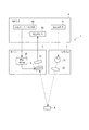
図1は、本実施形態の測色装置1(電子機器)の概略構成を示すブロック図である。
測色装置1は、図1に示すように、検査対象Aに光を射出する光源装置2と、測色センサー3(光学モジュール)と、測色装置1の全体動作を制御する制御装置4とを備える。そして、この測色装置1は、光源装置2から射出される光を検査対象Aにて反射させ、反射された検査対象光を測色センサー3にて受光し、測色センサー3から出力される検出信号に基づいて、検査対象光の色度、すなわち検査対象Aの色を分析して測定する装置である。
Hereinafter, an embodiment according to the present invention will be described with reference to the drawings.
[1. (Schematic configuration of the color measuring device)
FIG. 1 is a block diagram illustrating a schematic configuration of a color measurement device 1 (electronic device) according to the present embodiment.
As shown in FIG. 1, the
〔2.光源装置の構成〕
光源装置2は、光源21、複数のレンズ22(図1には1つのみ記載)を備え、検査対象Aに対して白色光を射出する。また、複数のレンズ22には、コリメーターレンズが含まれてもよく、この場合、光源装置2は、光源21から射出された白色光をコリメーターレンズにより平行光とし、図示しない投射レンズから検査対象Aに向かって射出する。なお、本実施形態では、光源装置2を備える測色装置1を例示するが、例えば検査対象Aが液晶パネルなどの発光部材である場合、光源装置2が設けられない構成としてもよい。
[2. Configuration of light source device]
The
〔3.測色センサーの構成〕
測色センサー3は、図1に示すように、波長可変干渉フィルター5と、波長可変干渉フィルター5を透過する光を受光する検出部31と、波長可変干渉フィルター5で透過させる光の波長を可変する電圧制御部32とを備える。また、測色センサー3は、波長可変干渉フィルター5に対向する位置に、検査対象Aで反射された反射光(検査対象光)を、内部に導光する図示しない入射光学レンズを備えている。そして、この測色センサー3は、波長可変干渉フィルター5により、入射光学レンズから入射した検査対象光のうち、所定波長の光を分光し、分光した光を検出部31にて受光する。
検出部31は、複数の光電交換素子により構成されており、受光量に応じた電気信号を生成する。そして、検出部31は、制御装置4に接続されており、生成した電気信号を受光信号として制御装置4に出力する。
[3. (Configuration of colorimetric sensor)
As shown in FIG. 1, the colorimetric sensor 3 has a variable
The
(3−1.波長可変干渉フィルターの構成)
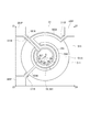
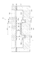
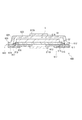
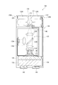
図2は、波長可変干渉フィルター5の概略構成を示す平面図であり、図3は、波長可変干渉フィルター5の概略構成を示す断面図である。
波長可変干渉フィルター5は、図2に示すように、例えば平面正方形状の板状の光学部材である。この波長可変干渉フィルター5は、図3に示すように、本発明の第二基板である固定基板51、および本発明の第一基板である可動基板52を備えている。これらの固定基板51及び可動基板52は、それぞれ例えば、ソーダガラス、結晶性ガラス、石英ガラス、鉛ガラス、カリウムガラス、ホウケイ酸ガラス、無アルカリガラスなどの各種ガラスや、水晶などにより形成されている。そして、これらの固定基板51及び可動基板52は、外周部近傍に形成される第一接合部523、第二接合部513が、例えばシロキサンを主成分とするプラズマ重合膜などにより構成された接合膜53により接合されることで、一体的に構成されている。
(3-1. Configuration of wavelength tunable interference filter)
FIG. 2 is a plan view showing a schematic configuration of the variable
As shown in FIG. 2, the variable
固定基板51には、本発明の第二反射膜を構成する固定反射膜54が設けられ、可動基板52には、本発明の第一反射膜を構成する可動反射膜55が設けられている。ここで、固定反射膜54は、固定基板51の可動基板52に対向する面に、本発明の第二電極である帯電防止電極561を介して設けられる。また、可動反射膜55は、可動基板52の固定基板51に対向する面に、本発明の第一電極である可動電極562を介して固定されている。また、これらの固定反射膜54および可動反射膜55は、反射膜間ギャップG1を介して対向配置されている。
波長可変干渉フィルター5には、固定反射膜54および可動反射膜55の間の反射膜間ギャップG1の寸法を調整するのに用いられる静電アクチュエーター56が設けられている。この静電アクチュエーター56は、固定基板51に設けられた固定内側電極563(本発明の内側駆動用電極)と、固定外側電極564(本発明の外側駆動用電極)と、前述の可動電極562とにより構成されている。ここで、これらの電極561,562,563,564は、それぞれ固定基板51及び可動基板52の基板表面に直接設けられる構成であってもよく、他の膜部材を介して設けられる構成であってもよい。
また、波長可変干渉フィルター5を固定基板51(可動基板52)の基板厚み方向から見た図2に示すような平面視において、固定基板51及び可動基板52の平面中心点Oは、固定反射膜54及び可動反射膜55の中心点と一致し、かつ後述する可動部521の中心点と一致する。ここで、固定基板51または可動基板52の基板厚み方向から見た平面視、つまり、固定基板51、接合膜53、及び可動基板52の積層方向から波長可変干渉フィルター5を見た平面視を、フィルター平面視とする。
The fixed
The wavelength
Further, in a plan view as shown in FIG. 2 in which the wavelength
(3−1−1.固定基板の構成)
図4は、第一実施形態の固定基板を可動基板側から見た平面視である。
固定基板51は、厚みが例えば500μmに形成されるガラス基材を加工することで形成される。具体的には、図3、図4に示すように、固定基板51には、エッチングにより電極配置溝511が形成されている。
また、この固定基板51は、可動基板52に対して厚み寸法が大きく形成されており、帯電防止電極561および可動電極562間に電圧を印加した際の静電引力や、帯電防止電極561,固定内側電極563,固定外側電極564の内部応力による固定基板51の撓みはない。
(3-1-1. Configuration of Fixed Substrate)
FIG. 4 is a plan view of the fixed substrate of the first embodiment as viewed from the movable substrate side.
The fixed
Further, the fixed
電極配置溝511は、フィルター平面視で、固定基板51の平面中心点Oを中心とした円形状に形成されている。ここで、電極配置溝511の溝底面は、帯電防止電極561,固定内側電極563,固定外側電極564が配置される電極固定面511Aとなる。
また、固定基板51には、電極配置溝511から、固定基板51の外周縁の各頂点C1,C2,C3に向かって延出する3つの電極引出溝511Bが設けられている。
The
The fixed
電極固定面511Aには、平面中心点Oを中心とした半径R1の光干渉領域Ar1を含む円領域に帯電防止電極561(本発明の第二電極)が形成されている。ここで、光干渉領域Ar1とは、波長可変干渉フィルター5に光を入射させた際に、光の多重干渉により目的波長の光が取り出される領域である。具体的には、固定反射膜54及び可動反射膜55が互いに対向している領域(フィルター平面視において、固定反射膜54及び可動反射膜55が重なり合う領域)である。
なお、本実施形態では、帯電防止電極561が円形状の光干渉領域Ar1に設けられる構成としたが、円形状の外周部の一部が欠ける構成などであってもよく、さらには、円形に限られず矩形状に形成されるものであってもよい。
また、電極固定面511A及び固定基板51の頂点C1に向かう電極引出溝511B上には、帯電防止電極561の外周縁から延出する帯電防止引出電極561Aが設けられている。この帯電防止引出電極561Aは、帯電防止電極561の外周縁から、固定基板51の頂点C1まで延出形成され、その先端部(固定基板51の頂点C1に位置する部分)が、電圧制御部32に接続される帯電防止電極パッド561Pを構成する。
On the
In the present embodiment, the
In addition, on the
また、電極固定面511Aには、固定内側電極563が形成されている。固定内側電極563は、帯電防止電極561の外周側に、帯電防止電極561や帯電防止引出電極561Aと非接触に形成されている。この固定内側電極563は、平面中心点Oを中心として半径R2〜R3の円環領域内に略C字状に設けられている。そして、この固定内側電極563のC字開口部分は、平面中心点Oから頂点C1に向かう方向に形成され、当該C字開口部分に、上記帯電防止引出電極561Aが配線される。
また、電極固定面511A及び固定基板51の頂点C2に向かう電極引出溝511B上には、固定内側引出電極563Aが設けられている。この固定内側引出電極563Aは、固定内側電極563のC字開口端部から、径外方向に電極配置溝511の外周縁まで延出し、そこから電極配置溝511の外周縁に沿って、頂点C2に対応した電極引出溝511Bまで延出し、更に電極引出溝511Bに沿って頂点C2まで延出する。この固定内側引出電極563Aの先端部(固定基板51の頂点C2に位置する部分)は、電圧制御部32に接続される固定内側電極パッド563Pを構成する。
A fixed
A fixed
更に、電極固定面511Aには、固定外側電極564が形成されている。固定外側電極564は、固定内側電極563の外周側に、固定内側電極563,固定内側引出電極563A,帯電防止引出電極561Aと非接触に形成されている。この固定外側電極564は、平面中心点Oを中心とした半径R4〜R5の円環領域に略C字状に設けられ、このC字開口部分に、上記帯電防止引出電極561A及び固定内側引出電極563Aが配線される。
また、電極固定面511A及び固定基板51の頂点C3に向かう電極引出溝511B上には、固定外側引出電極564Aが設けられている。この固定外側引出電極564Aは、固定外側電極564の外周縁から、固定基板51の頂点C3まで延出形成されている。また、固定外側引出電極564Aの先端部(固定基板51の頂点C3に位置する部分)は、電圧制御部32に接続される固定外側電極パッド564Pを構成する。
Further, a fixed
Further, a fixed
ここで、帯電防止電極561(帯電防止引出電極561A)は、透光性の導電膜(例えばITO:Indium Tin Oxide)により形成されており、波長可変干渉フィルター5に導入された光や、固定反射膜54,可動反射膜55間で多重干渉により取り出された光を透過させる。なお、本実施形態では、検査対象Aの測色を実施するため、可視光域を検査対象波長域としているが、例えば、赤外光等、可視光以外を検査対象光とする場合では、その検査対象光を透過可能な導電膜を用いる。
また、固定内側電極563(固定内側引出電極563A),固定外側電極564(固定外側引出電極564A)は、上記帯電防止電極561と同様の導電膜により構成されることが好ましい。帯電防止電極561、固定内側電極563、及び固定外側電極564が同一の導電膜である場合、配線形成時に、一工程でこれらの帯電防止電極561,固定内側電極563,固定外側電極564を形成することができ、製造効率の向上を図ることができる。なお、本実施形態では、各電極561,563,564が同一の導電膜材料により構成される例を示すが、例えば固定内側電極563及び固定外側電極564を、帯電防止電極561と異なる導電膜により構成してもよく、固定内側電極563及び固定外側電極564が異なる導電膜であってもよい。
Here, the antistatic electrode 561 (
The fixed inner electrode 563 (fixed
そして、帯電防止電極561上には、光干渉領域Ar1に円形の固定反射膜54が設けられている。
この固定反射膜54としては、金属膜により形成されるものであってもよく、誘電体多層膜により形成されるものであってもよく、さらには、誘電多層膜上にAg合金が形成される構成などとしてもよい。金属単層膜としては、例えばAgや、Ag合金の単層膜を用いることができる。また、誘電体多層膜の場合は、例えば高屈折層をTiO2、低屈折層をSiO2とした誘電体多層膜を用いることができ、表層をAg合金等の導電性の反射膜で覆うことで、確実に帯電防止電極561との導通を取る構成としてもよい。
On the
The fixed
また、固定基板51には、可動基板52とは反対側の面において、固定反射膜54に対応する位置に反射防止膜が形成されていてもよい。このような反射防止膜は、低屈折率膜および高屈折率膜を交互に積層することで形成することができ、固定基板51の表面での可視光の反射率を低下させ、透過率を増大させることができる。
Further, an antireflection film may be formed on the fixed
(3−1−2.可動基板の構成)
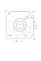
図5は、第一実施形態の可動基板を固定基板側から見た平面視である。
可動基板52は、厚みが例えば200μmに形成されるガラス基材をエッチングにより加工することで形成されている。
具体的には、可動基板52は、図2、図5に示すようなフィルター平面視において、平面中心点Oを中心とした円形状の可動部521と、可動部521と同軸であり可動部521を保持する保持部522と、を備えている。
また、可動基板52には、図2、図5に示すように、頂点C1,C2,C3に対応して、切欠部524が形成されており、波長可変干渉フィルター5を可動基板52側から見た面に、帯電防止電極パッド561P,固定内側電極パッド563P,固定外側電極パッド564Pが露出する。
(3-1-2. Configuration of movable substrate)
FIG. 5 is a plan view of the movable substrate of the first embodiment viewed from the fixed substrate side.
The
Specifically, the
Further, as shown in FIGS. 2 and 5, the
可動部521は、保持部522よりも厚み寸法が大きく形成され、例えば、本実施形態では、可動基板52の厚み寸法と同一寸法である200μmに形成されている。この可動部521は、フィルター平面視において、少なくとも固定外側電極564の外周縁の径寸法よりも大きい径寸法に形成されている。つまり、可動部521は、フィルター平面視において、半径R5以上の円形状に形成されている。
なお、固定基板51と同様に、可動部521の固定基板51とは反対側の面には、反射防止膜が形成されていてもよい。このような反射防止膜は、低屈折率膜および高屈折率膜を交互に積層することで形成することができ、可動基板52の表面での可視光の反射率を低下させ、透過率を増大させることができる。
The
Similar to the fixed
そして、可動部521の固定基板51に対向する可動面521Aには、固定内側電極563や固定外側電極564と、電極間ギャップG2を介して対向する可動電極562が設けられている。
この可動電極562は、第二基板の光干渉領域Ar1を含む可動面521Aの全面に亘って設けられている。つまり、可動電極562は、可動面521A上で、平面中心点Oを中心とした半径R5の円形領域内に設けられている。可動電極562は、帯電防止電極561と同様に、例えばITO等の透光性の導電膜により形成されている。なお、本発明において、可動電極562が可動面521Aの全面に亘って設けられるとは、可動電極562が可動面521Aの略全面に亘って設けられる構成をも含むものである。すなわち、本発明の目的を達成することが可能な範囲であれば、僅かな誤差は含まれるものである。具体的には、可動電極562は、平面中心点Oからの半径が、少なくとも固定外側電極564の外周縁の半径R5以上、可動面の外周縁の半径以下に形成されていればよい。
The
The
また、可動基板52には、可動電極562の外周縁から延出する可動引出電極562Aが設けられている。この可動引出電極562Aは、可動電極562の外周縁から、可動基板52の頂点C1に向かって延出する。そして、この可動引出電極562Aの先端部は、頂点C1において、帯電防止電極パッド561Pと対向し、例えばAgペースト等の導電性部材562Bを介して、帯電防止電極パッド561Pに接続される。ここで、この帯電防止電極パッド561Pは、電圧制御部32によりGND回路に接続されており、接地されている。したがって、可動電極562及び帯電防止電極561は、0電位に維持されている。
The
そして、フィルター平面視において、可動電極562は、固定内側電極563に対向する内側駆動用電極対向領域5621及び、固定外側電極564に対向する外側駆動用電極対向領域5622を有している。したがって、固定内側電極563及び固定外側電極564の電位を所定値に設定することで、固定内側電極563及び内側駆動用電極対向領域5621間、固定外側電極564及び内側駆動用電極対向領域5621間にそれぞれ電位差が生じ、静電引力が発生する。すなわち、可動電極562,固定内側電極563,固定外側電極564により本発明のギャップ変更部である静電アクチュエーター56が構成される。
In the filter plan view, the
また、可動電極562のうち、フィルター平面視において、光干渉領域Ar1と重なる位置には、可動反射膜55が設けられている。この可動反射膜55は、上述した固定反射膜54と同一の構成、同一径寸法の反射膜が用いられている。
In addition, a movable
保持部522は、可動部521の周囲を囲うダイアフラムであり、例えば厚み寸法が50μmに形成され、可動部521よりも厚み方向に対する剛性が小さく形成されている。
このため、保持部522は可動部521よりも撓みやすく、僅かな静電引力により固定基板51側に撓ませることが可能となる。この際、可動部521は、保持部522よりも厚み寸法が大きく、剛性が大きくなるため、静電引力により可動基板52を撓ませる力が作用した場合でも、可動部521の撓みはほぼなく、可動部521に形成された可動反射膜55の撓みも防止できる。
なお、本実施形態では、ダイアフラム状の保持部522を例示するが、これに限定されず、例えば、平面中心点Oを中心として、等角度間隔で配置された梁状の保持部が設けられる構成などとしてもよい。
The holding
For this reason, the holding
In this embodiment, the diaphragm-
(3−2.電圧制御手段の構成)
電圧制御部32は、GND回路を有し、帯電防止電極パッド561Pを接地している。これにより、上述したように、帯電防止電極パッド561Pに接続された帯電防止電極561,可動電極562は0電位に維持される。また、電圧制御部32は、固定内側電極パッド563P,固定外側電極パッド564Pに接続され、制御装置4からの入力される制御信号に基づいて、これらの固定内側電極パッド563P及び固定外側電極パッド564Pを所定の電位に設定し、静電アクチュエーター56に電圧を印加して駆動させる。
(3-2. Configuration of voltage control means)
The
〔4.制御装置の構成〕
制御装置4は、測色装置1の全体動作を制御する。
この制御装置4としては、例えば汎用パーソナルコンピューターや、携帯情報端末、その他、測色専用コンピューターなどを用いることができる。
そして、制御装置4は、図1に示すように、光源制御部41、測色センサー制御部42、および本発明の分析処理部を構成する測色処理部43などを備えて構成されている。
光源制御部41は、光源装置2に接続されている。そして、光源制御部41は、例えば利用者の設定入力に基づいて、光源装置2に所定の制御信号を出力し、光源装置2から所定の明るさの白色光を射出させる。
測色センサー制御部42は、測色センサー3に接続されている。そして、測色センサー制御部42は、例えば利用者の設定入力に基づいて、測色センサー3にて受光させる光の波長を設定し、この波長の光の受光量を検出する旨の制御信号を測色センサー3に出力する。これにより、測色センサー3の電圧制御部32は、制御信号に基づいて、利用者が所望する光の波長のみを透過させるよう、静電アクチュエーター56への印加電圧を設定する。
測色処理部43は、検出部31により検出された受光量から、検査対象Aの色度を分析する。
[4. Configuration of control device]
The control device 4 controls the overall operation of the
As the control device 4, for example, a general-purpose personal computer, a portable information terminal, other color measurement dedicated computer, or the like can be used.
As shown in FIG. 1, the control device 4 includes a light
The light
The colorimetric
The
〔5.実施形態の作用効果〕
本実施形態の波長可変干渉フィルター5では、可動基板52の可動面521Aの全面に可動電極562が設けられ、この可動電極562上に可動反射膜55が設けられている。また、固定基板51の電極配置溝511には、帯電防止電極561が設けられ、この帯電防止電極561上に固定反射膜54が設けられている。そして、可動電極562及び帯電防止電極561は、導電部材により電気的に接続され、かつ、電圧制御部32のGND回路により接地されている。
このため、固定反射膜54及び可動反射膜55が0電位に維持され、固定反射膜54や可動反射膜55への帯電物質の付着を防止することができる。また、固定反射膜54及び可動反射膜55が同電位となる。このため、固定反射膜54及び可動反射膜55間での静電引力等のクーロン力の発生がなく、静電アクチュエーター56により精度よく反射膜間ギャップG1の寸法を所望の値に変化させることができる。
また、フィルター平面視において、可動電極562が可動部521の全面に設けられ、かつ接地されているため、シールド効果を得ることができ、電磁波の影響を抑制することができる。すなわち、電磁波により、固定内側電極563や固定外側電極564に設定された電位が変動することで、本来波長可変干渉フィルター5を透過させた目的波長以外のノイズ成分の光が当該波長可変干渉フィルター5を透過してしまう不都合を抑制できる。したがって、測色センサー3において精度の高い目的波長の光の光量検出を実施することができ、測色装置1において、検査対象Aの正確に色度を測定することができる。
さらに、本実施形態の波長可変干渉フィルター5では、固定基板51の固定反射膜54と重なる光干渉領域Ar1に帯電防止電極561が設けられることで、上述のシールド効果をより効果的に発揮させることができ、電磁波の影響をより確実になくすことができる。
[5. (Effects of Embodiment)
In the variable
For this reason, the fixed
In addition, since the
Furthermore, in the wavelength
また、可動電極562及び帯電防止電極561は、透光性の導電膜であるITOにより形成されている。このため、波長可変干渉フィルター5に入射する光、波長可変干渉フィルター5により取り出された光を透過させることができる。
The
そして、可動電極562は、可動部521の全面を覆って設けられ、固定基板51に設けられた固定内側電極563に対向する内側駆動用電極対向領域5621、固定外側電極564に対向する外側駆動用電極対向領域5622を有する。
このため、可動基板52に固定内側電極563や固定外側電極564と対向する別電極を形成する必要がなく、可動電極562、固定内側電極563、及び固定外側電極564により静電アクチュエーター56を構成することができる。したがって、配線構造を簡略化することができ、波長可変干渉フィルター5を測色センサー3に組み込む際の配線作業等を簡略化することができる。
また、固定内側電極563及び固定外側電極564に対してそれぞれ別の電位を設定することができ、固定内側電極563及び内側駆動用電極対向領域5621で発生させる静電引力、固定外側電極564及び外側駆動用電極対向領域5622で発生させる静電引力を異ならせることができる。したがって、可動部521の変位量をより精密に制御することができる。
The
For this reason, it is not necessary to form another electrode facing the fixed
Further, different potentials can be set for the fixed
[第二実施形態]
次に、本発明の第二実施形態について、図面に基づいて説明する。
上記第一実施形態では、固定基板51に対して光干渉領域Ar1に帯電防止電極561を設け、この帯電防止電極561上に固定反射膜54を設ける例を示した。これに対して、本実施形態では、第二基板である固定基板に対して、直接第二反射膜である固定反射膜が設けられ、当該固定反射膜が、第一電極である可動電極に導通される点で、上記第一実施形態と相違する。
つまり、反射膜として、例えばAg合金等の導電性の反射膜を用いる場合、必ずしも第二電極である固定側帯電防止電極を設ける必要はなく、第二反射膜が第一電極に導通していれば、本発明の目的と達成することができる。本実施形態では、このような例について以下に説明する。
[Second Embodiment]
Next, a second embodiment of the present invention will be described based on the drawings.
In the first embodiment, the example in which the
That is, when a conductive reflective film such as an Ag alloy is used as the reflective film, it is not always necessary to provide the fixed-side antistatic electrode that is the second electrode, and the second reflective film may be electrically connected to the first electrode. Thus, the object of the present invention can be achieved. In the present embodiment, such an example will be described below.
図6は、第二実施形態の波長可変干渉フィルターの概略構成を示す断面図である。
なお、第二実施液体以降の説明に当たり、上記第一実施形態と同様の構成については、同符号を付し、その説明を省略する。
図6において、波長可変干渉フィルター5Aは、第一実施形態の波長可変干渉フィルター5と同様に、固定基板51及び可動基板52を備えている。
そして、本実施形態の固定基板51は、フィルター平面視において、光干渉領域Ar1と重なる位置に、電極固定面511A上に直接、導電性の固定反射膜54が設けられている。ここで固定反射膜54としては、導電性を有していれば、いかなる反射膜を用いてもよく、例えば、Ag等の金属膜や、Ag合金等の合金膜を用いることができる。
FIG. 6 is a cross-sectional view illustrating a schematic configuration of a wavelength tunable interference filter according to the second embodiment.
In the description after the second embodiment liquid, the same reference numerals are given to the same configurations as those in the first embodiment, and the description thereof is omitted.
In FIG. 6, the variable
The fixed
また、図示は省略するが、固定基板51には、この固定反射膜54の外周縁から延出する帯電防止引出電極(図示略)が設けられている。この帯電防止引出電極は、第一実施形態と同様に、固定反射膜54から、固定基板51の頂点C1(図2参照)に向かって延出し、先端部において、帯電防止電極パッドを構成する。また、帯電防止電極パッドは、頂点C1近傍において、可動基板52に設けられた可動引出電極562Aに、例えばAgペースト等の導電性部材で接続される。これにより、可動電極562と固定反射膜54とが電気的に導通される。
また、第一実施形態と同様に、帯電防止電極パッドは、電圧制御部32に接続され、電圧制御部32に設けられたGND回路により接地されている。
Although not shown, the fixed
Similarly to the first embodiment, the antistatic electrode pad is connected to the
上述のような第二実施形態では、第一実施形態と同様の効果が得られる。
すなわち、第二実施形態の波長可変干渉フィルター5Aでは、可動基板52の可動面521Aの全面に可動電極562が設けられ、この可動電極562上に可動反射膜55が設けられ、可動電極562が固定基板51に設けられる固定反射膜54と電気的に接続される。そして、可動電極562及び固定反射膜54は、導電部材により電気的に接続され、かつ、電圧制御部32のGND回路により接地されている。
このため、固定反射膜54及び可動反射膜55が0電位に維持され、固定反射膜54や可動反射膜55への帯電物質の付着を防止することができ、固定反射膜54及び可動反射膜55間での静電引力等のクーロン力の発生を防止できる。これにより、静電アクチュエーター56により精度よく反射膜間ギャップG1の寸法を所望の値に変化させることができる。
また、フィルター平面視において、可動電極562が可動部521の全面に設けられ、かつ接地されているため、シールド効果を得ることができ、電磁波の影響を抑制することができる。
In the second embodiment as described above, the same effects as in the first embodiment can be obtained.
That is, in the wavelength
For this reason, the fixed
In addition, since the
また、本実施形態では、固定基板51上に帯電防止電極561が設けられないため、その分構成を簡略化することができ、製造コストも低減させることができ、製造効率性も向上させることができる。
In the present embodiment, since the
[第三実施形態]
次に、本発明の第三実施形態について、図面に基づいて説明する。
上記第一及び第二実施形態では、本発明の第一基板を可動基板52とし、可動基板52の可動部521の全面に亘って第一電極である可動電極562を設ける構成とした。これに対して、第三実施形態では、本発明の第一基板を固定基板とし、固定基板に第一電極である固定電極を設ける点で上記第一及び第二実施形態と相違する。
図7は、第三実施形態の波長可変干渉フィルターの概略構成を示す断面図である。
[Third embodiment]
Next, a third embodiment of the present invention will be described based on the drawings.
In the first and second embodiments, the first substrate of the present invention is the
FIG. 7 is a cross-sectional view illustrating a schematic configuration of a wavelength tunable interference filter according to the third embodiment.
第三実施形態の波長可変干渉フィルター5Bでは、本発明の第一基板を構成する固定基板51と、本発明の第二基板を構成する可動基板52と、を備えている。
可動基板52は、フィルター平面視において、平面中心点Oを中心とした円形の可動部521と、可動部521と同軸であり可動部521を保持する保持部522と、を備えている。
The wavelength
The
そして、本実施形態では、可動部521の可動面521Aには、平面中心点Oを中心とする半径R1の可動反射膜55と、可動反射膜55の外周側で、可動反射膜55と非接触で設けられた略C字状の可動内側電極566(本発明の内側駆動用電極)と、可動内側電極566の外周側で、可動反射膜55及び可動内側電極566と非接触で設けられた略C字状の可動外側電極567(本発明の外側駆動用電極)と、を備えている。
ここで、図示は省略するが、可動内側電極566は、外周縁から可動基板52の外周部(例えば頂点)に向かって延出する内側可動引出電極を備えており、この内側可動引出電極の端部は、電圧制御部32に接続される内側可動電極パッドを構成している。同様に、可動外側電極567は、外周縁から可動基板52の外周部に向かって延出する外側可動引出電極を備えており、この外側可動引出電極の端部は、電圧制御部32に接続される外側可動電極パッドを構成している。
また、図示は省略するが、可動基板52には、可動反射膜55の外周縁から、可動基板52の外周部に向かって延出する接続電極を備え、接続電極の端部において、後述する固定電極565に接続されている。
なお、これらの接続電極、内側可動引出電極、及び外側可動引出電極の電極形状(配線位置)については、図4と略同様の電極引き回し形状を用いることができる。
In this embodiment, the
Here, although illustration is omitted, the movable
Although illustration is omitted, the
In addition, about the electrode shape (wiring position) of these connection electrodes, an inner side movable extraction electrode, and an outer side movable extraction electrode, the electrode routing shape substantially the same as FIG. 4 can be used.
保持部522は、上記第一実施形態と同様の構成であるため、ここでの説明は省略する。
Since the holding
固定基板51は、図7に示すように、エッチングにより形成された電極配置溝511および反射膜固定部512を備えている。また、この固定基板51は、上記第一実施形態及び第二実施形態と同様に、可動基板52に対して厚み寸法が大きく形成されており、静電引力等による固定基板51の撓みはない。
As shown in FIG. 7, the fixed
電極配置溝511は、フィルター平面視で、円環形状に形成されている。反射膜固定部512は、電極配置溝511の中心部から、可動基板52側に突出して形成される。また、反射膜固定部512の可動基板52に対向する反射膜固定面512Aは、フィルター平面視において光干渉領域Ar1と重なり、本発明の第一反射膜である固定反射膜54が設けられる。すなわち、反射膜固定面512Aは、平面中心点Oを中心とした、半径が半径R1の円形状に形成されている。
また、固定基板51には、上記実施形態と同様に、電極配置溝511から延出する電極引出溝(図示略)が設けられている。
The
In addition, the fixed
固定基板51の可動基板52に対向する面には、フィルター平面視において、可動部521と重なる領域(可動部対向領域Ar2)の全体に亘って、本発明の第一電極である固定電極565が設けられている。この固定電極565としては、例えばITO等の透光性を有する導電膜が用いられている。
このような構成では、フィルター平面視において、固定電極565のうち、可動内側電極566に対向する部分が内側駆動用電極対向領域5651となり、可動外側電極567に対向する部分が外側駆動用電極対向領域5652となる。したがって、可動内側電極566及び可動外側電極567の電位を所定値に設定することで、可動内側電極566及び内側駆動用電極対向領域5651間、可動外側電極567及び外側駆動用電極対向領域5652間にそれぞれ電位差が生じ、静電引力が発生する。すなわち、固定電極565,可動内側電極566,可動外側電極567により静電アクチュエーター56が構成される。
On the surface of the fixed
In such a configuration, the portion of the fixed
また、図示は省略するが、固定基板51には、固定電極565の外周縁から延出する固定引出電極が設けられており、この固定引出電極の端部は、帯電防止電極パッドを構成する。また、この固定引出電極の端部は、可動反射膜55から延出した配線電極が対向し、例えばAgペースト等の導電部材を介して、これらの固定引出電極及び配線電極が接続される。また、この帯電防止電極パッドは、電圧制御部32によりGND回路に接続されており、接地されている。
Although not shown, the fixed
そして、反射膜固定面512A上の固定電極565には、固定反射膜54が積層されている。したがって、本実施形態では、固定反射膜54及び可動反射膜55の間の反射膜間ギャップG1は、可動内側電極566及び内側駆動用電極対向領域5651間(可動外側電極567及び外側駆動用電極対向領域5652間)の電極間ギャップG2よりも小さくなる。
A fixed
上述のような第三実施形態の波長可変干渉フィルター5Bでは、上記第一及び第二実施形態の効果に加え、次の効果が得られる。
波長可変干渉フィルター5Bでは、固定基板51の可動部対向領域Ar2の全体に固定電極565が設けられている。このため、固定電極565の膜応力を考慮することなく、簡単な構成で、固定反射膜54及び可動反射膜55の帯電を防止可能な波長可変干渉フィルター5Bが得られる。
つまり、第一及び第二実施形態のように、可動基板52の広範囲に可動電極562を設ける構成では、可動電極562の膜応力により可動基板52が撓むおそれがある。この場合、膜応力による基板の撓みを防止するために、可動電極562の膜応力を打ち消す撓み防止膜を別途設ける等の対策が必要になる場合がある。
これに対して、本実施形態では、撓みが発生しにくい固定基板51に固定電極565を設けているので、広範囲に亘って固定電極565の膜応力が発生した場合でも、その影響を受けにくく、固定基板51の撓みが発生しない。このため、固定反射膜54の撓みも生じず、固定反射膜54及び可動反射膜55を平行に維持することができ、波長可変干渉フィルター5Bの分解能の低下を防止することができる。また、膜応力に対して、別途撓み防止膜を設ける等の対策が不要であり、簡単な構成で固定反射膜54及び可動反射膜55の帯電を防止可能な波長可変干渉フィルター5Bが得られる。
In the wavelength
In the variable
That is, in the configuration in which the
On the other hand, in this embodiment, since the fixed
また、反射膜間ギャップG1が電極間ギャップG2よりも小さいため、反射膜間ギャップの変動可能領域を大きくでき、測色装置1の測定可能波長域を広域化することができる。これに加え、帯電防止電極561,可動電極562間での静電引力の制御が容易となり、反射膜間ギャップの寸法をより精度よく、所望の値に設定することができる。
Moreover, since the gap G1 between the reflection films is smaller than the gap G2 between the electrodes, the changeable region of the gap between the reflection films can be increased, and the measurable wavelength range of the
[第四実施形態]
次に、上記第三実施形態を変形した第四実施形態について、図面に基づいて説明する。
第三実施形態の波長可変干渉フィルター5Bは、可動内側電極566及び内側駆動用電極対向領域5651間の寸法と、可動外側電極567及び外側駆動用電極対向領域5652間の寸法を同一の寸法とした。これに対して、第四実施形態の波長可変干渉フィルターは、可動内側電極及び内側駆動用電極対向領域間の寸法と、可動外側電極及び外側駆動用電極対向領域間の寸法とが異なる点で、上記第三実施形態と相違する。
図8は、第四実施形態の波長可変干渉フィルターの概略構成を示す断面図である。
[Fourth embodiment]
Next, a fourth embodiment obtained by modifying the third embodiment will be described with reference to the drawings.
In the wavelength
FIG. 8 is a cross-sectional view illustrating a schematic configuration of a wavelength tunable interference filter according to the fourth embodiment.
本実施形態の波長可変干渉フィルター5Cでは、固定基板51は、電極配置溝511と、反射膜固定部512と、第二電極配置溝514と、を備えている。
ここで、第二電極配置溝514は、電極配置溝511の外周側に形成され、電極配置溝511の電極固定面511Aよりも浅い円環形状の溝である。すなわち、可動部521が変位していない初期状態において、電極固定面511A及び可動面521A間の距離、反射膜固定面512A及び可動面521A間の距離、第二電極配置溝514の底面である第二の電極固定面514A及び可動面521A間の距離を比較すると、「反射膜固定面512A及び可動面521A間の距離」<「第二電極固定面514A及び可動面521A間の距離」<「電極固定面511A及び可動面521Aの距離」となる。
In the wavelength
Here, the second
また、可動基板52において、可動内側電極566は、電極配置溝511の電極固定面511Aに対向する位置に設けられており、可動外側電極567は、第二の電極固定面514Aに対向する位置に設けられている。したがって、固定基板51に設けられた固定電極565のうち、可動内側電極566に対向する内側駆動用電極対向領域5651は、電極固定面511A上の領域となり、可動外側電極567に対向する外側駆動用電極対向領域5652は、第二の電極固定面514A上の領域となる。このような構成では、可動内側電極566及び内側駆動用電極対向領域5651間の内側電極間ギャップG3、可動外側電極567及び外側駆動用電極対向領域5652間の外側電極間ギャップG4、及び固定反射膜54及び可動反射膜55間の反射膜間ギャップG1は、G1<G4<G3の関係となる。
In the
このような第四実施形態では、上記第三実施形態の効果に加え、更に、静電アクチュエーター56による反射膜間ギャップG1の制御を精度よく、かつ効率的に実施することができるという効果を奏することができる。
つまり、可動部521を固定基板51側に所定量だけ撓ませるために必要となる力は、接合膜53により接合された部位に近づくほど大きくなる。したがって、例えば、「(内側電極間ギャップG3)=(外側電極間ギャップG4)」となる構成では、可動部521を変動させるために、可動外側電極567に設定する電位を大きくして、より大きい静電引力を作用させる必要がある。これに対して、本実施形態のように、外側電極間ギャップG4の寸法を内側電極間ギャップG3よりも小さくすることで、可動外側電極567及び外側駆動用電極対向領域5652間に印加する電圧を小さくすることができ、効率的に可動部521を駆動させることができ、省電力化を図ることができる。
In the fourth embodiment, in addition to the effects of the third embodiment, there is an effect that the control of the inter-reflective film gap G1 by the
That is, the force required to bend the
[第五実施形態]
次に、本発明の第五実施形態について、図面に基づいて説明する。
上記第一実施形態の測色装置1では、光学モジュールである測色センサー3に対して、波長可変干渉フィルター5が直接設けられる構成とした。この場合、測色センサー3に設けられた所定の配置位置に波長可変干渉フィルター5を設け、帯電防止電極パッド561Pや固定内側電極パッド563P、固定外側電極パッド564Pに対して配線を実施する。しかしながら、光学モジュールとしては、複雑な構成を有するものもあり、特に小型化の光学モジュールに対して、波長可変干渉フィルター5を直接設けることが困難な場合がある。本実施形態では、そのような光学モジュールに対しても、波長可変干渉フィルター5を容易に設置可能にする光学フィルターデバイスについて、以下に説明する。
図9は、本発明の第五実施形態に係る光学フィルターデバイスの概略構成を示す断面図である。
[Fifth embodiment]
Next, a fifth embodiment of the present invention will be described based on the drawings.
In the
FIG. 9 is a cross-sectional view showing a schematic configuration of an optical filter device according to the fifth embodiment of the present invention.
図9に示すように、光学フィルターデバイス600は、波長可変干渉フィルター5を収納する筐体610を備えている。
この筐体610は、底部611と、リッド612と、入射側ガラス窓613(導光部)と、射出側ガラス窓614(導光部)と、を有する。
As shown in FIG. 9, the
The
底部611は、例えば単層セラミック基板により構成される。この底部611には、波長可変干渉フィルター5の可動基板52が固定される。また、底部611には、波長可変干渉フィルター5の光干渉領域Ar1に対向する領域に、光入射孔611Aが開口形成されている。この光入射孔611Aは、波長可変干渉フィルター5により分光したい入射光(検査対象光)が入射される窓であり、入射側ガラス窓613が接合されている。なお、底部611及び入射側ガラス窓613の接合としては、例えば、ガラス原料を高温で熔解し、急冷したガラスのかけらであるガラスフリットを用いたガラスフリット接合を用いることができる。
The bottom 611 is constituted by, for example, a single layer ceramic substrate. The
また、底部611の上面(筐体610の内部側)には、波長可変干渉フィルター5の各電極パッド561P,563P,564Pに対応した数の端子部616が設けられている。また、底部611は、各端子部616が設けられる位置に、貫通孔615が形成されており、各端子部616は、貫通孔615を介して、底部611の下面(筐体610の外部側)に設けられた接続端子617に接続されている。
また、底部611の外周縁には、リッド612に接合される封止部619が設けられている。
In addition, a number of
Further, a sealing
リッド612は、図9に示すように、底部611の封止部619に接合される封止部620と、封止部620から連続し、底部611から離れる方向に立ち上がる側壁部621と、側壁部621から連続し、波長可変干渉フィルター5の固定基板51側を覆う天面部622とを備えている。このリッド612は、例えばコバール等の合金または金属により形成することができる。
このリッド612は、封止部620と、底部611の封止部619とが、例えばレーザー封止等により接合されることで、底部611に接合されている。また、リッド612の天面部622には、波長可変干渉フィルター5の光干渉領域Ar1に対向する領域に、光射出孔612Aが開口形成されている。この光射出孔612Aは、波長可変干渉フィルター5により分光されて取り出された光が通過する窓であり、例えばガラスフリット接合等により射出側ガラス窓614が接合されている。
なお、筐体610内には、例えば窒素やアルゴンガス等の不活性ガスを封入する構成としてもよく、高い真空度に維持される構成としてもよい。このような構成とすることで、波長可変干渉フィルター5の反射膜54,55の劣化を防止できる。また、真空度を高い状態で維持される場合では、波長可変干渉フィルター5の静電アクチュエーター56に電圧を印加した際の、可動部521の応答性を向上させることができる。
As shown in FIG. 9, the
The
Note that the
このような光学フィルターデバイス600では、筐体610により波長可変干渉フィルター5が保護されているため、異物や大気に含まれるガス等による波長可変干渉フィルター5の特性変化を防止でき、また、外的要因による波長可変干渉フィルター5の破損を防止できる。したがって、測色センサー等の光学モジュールや電子機器に対して、波長可変干渉フィルター5を設置する際や、メンテナンス時において、他の部材との衝突等による破損を防止できる。
また、例えば工場で製造された波長可変干渉フィルター5を、光学モジュールや電子機器を組み立てる組み立てライン等まで運搬する場合に、筐体610により保護された波長可変干渉フィルター5では、安全に運搬することが可能となる。
また、光学フィルターデバイス600は、筐体610の外周面に露出する接続端子617が設けられているため、光学モジュールや電子機器に対して組み込む際にも容易に配線を実施することが可能となる。
In such an
For example, when the wavelength
Further, since the
なお、第五実施形態では、底部611に可動基板52が固定される構成を例示したが、これに限定されない。例えば、底部611に固定基板51が固定される構成などとしてもよい。
In the fifth embodiment, the configuration in which the
[他の実施形態]
なお、本発明は前述の実施形態に限定されるものではなく、本発明の目的を達成できる範囲での変形、改良等は本発明に含まれるものである。
[Other Embodiments]
It should be noted that the present invention is not limited to the above-described embodiments, and modifications, improvements, and the like within the scope that can achieve the object of the present invention are included in the present invention.
例えば、第一及び第二実施形態において、固定基板51に反射膜固定部512が設けられない構成としたが、第三及び第四実施形態の固定基板51のように、反射膜固定部512が設けられ、反射膜間ギャップG1が電極間ギャップよりも小さくなる構成としてもよい。
このような構成にすることで、第三実施形態や第四実施形態と同様に、反射膜間ギャップG1の変動可能領域を大きくでき、測色装置1の測定可能波長域を広域化することができる。また、静電アクチュエーター56による静電引力の制御が容易となり、反射膜間ギャップの寸法をより精度よく、所望の値に設定することができる。
For example, in the first and second embodiments, the reflective
By adopting such a configuration, as in the third embodiment and the fourth embodiment, the variable region of the gap G1 between the reflection films can be increased, and the measurable wavelength region of the
また、第一及び第二実施形態において、静電アクチュエーター56を構成する電極として、固定基板51に固定内側電極563及び固定外側電極564が設けられる例を示したが、これに限定されない。例えば、固定基板51に更に多くの駆動用電極が設けられる構成(例えば三重電極等)としてもよく、固定外側電極564が設けられず、固定内側電極563及び可動電極562により静電アクチュエーター56を構成するものであってもよい。第三及び第四実施形態においても同様であり、静電アクチュエーター56を構成する電極として、可動基板52に3つ以上の駆動用電極が設けられてもよく、単一の駆動用電極のみが設けられる構成としてもよい。
In the first and second embodiments, the example in which the fixed
また、上記実施形態では、ギャップ可変部として、静電アクチュエーター56を例示したが、これに限定されない。例えば、第一実施形態において、固定内側電極563,固定外側電極564の代わりに、誘電コイルを配置し、可動基板52に永久磁石を配置した誘電アクチュエーターを用いる構成としてもよい。
さらに、静電アクチュエーター56の代わりに圧電アクチュエーターを用いる構成としてもよい。この場合、例えば保持部522に下部電極層、圧電膜、および上部電極層を積層配置させ、下部電極層および上部電極層の間に印加する電圧を入力値として可変させることで、圧電膜を伸縮させて保持部522を撓ませる。
Moreover, in the said embodiment, although the
Further, a piezoelectric actuator may be used instead of the
また、上記第一実施形態では、波長可変干渉フィルター5において、帯電防止電極パッド561Pと可動引出電極562Aとが導電性部材562Bを介して電気的に接続されることで、固定反射膜54及び可動反射膜55を同電位にする構成としたが、これに限定されない。例えば、電圧制御部32等、波長可変干渉フィルター5の外部において、帯電防止電極パッド561P及び可動引出電極562Aが接続される構成としてもよい。また、帯電防止電極パッド561P及び可動引出電極562Aをそれぞれ別々に接地する構成としてもよい。
In the first embodiment, in the variable
また、上記実施形態では、固定基板51側から入射した光に対して、固定反射膜54,可動反射膜55間で光干渉させ、取り出された光を可動基板52側から射出させる波長可変干渉フィルター5を例示したが、これに限定されない。
例えば、固定反射膜54,可動反射膜55間での光干渉により取り出された光を、再び固定基板51側に射出させる構成としてもよい。この場合、例えば第一実施形態や第二実施形態のように、可動基板52側に本発明の第一電極である可動電極562を設ける場合、当該可動電極562として遮光性の導電部材を用いてもよい。
In the above embodiment, the wavelength variable interference filter that causes light incident from the fixed
For example, the light extracted by the light interference between the fixed
本発明の電子機器として、測色装置1を例示したが、その他、様々な分野により本発明の波長可変干渉フィルター、光学モジュール、電子機器を用いることができる。
例えば、特定物質の存在を検出するための光ベースのシステムとして用いることができる。このようなシステムとしては、例えば、本発明の波長可変干渉フィルターを用いた分光計測方式を採用して特定ガスを高感度検出する車載用ガス漏れ検出器や、呼気検査用の光音響希ガス検出器などのガス検出装置を例示できる。
このようなガス検出装置の一例を以下に図面に基づいて説明する。
Although the
For example, it can be used as a light-based system for detecting the presence of a specific substance. As such a system, for example, an in-vehicle gas leak detector that detects a specific gas with high sensitivity by adopting a spectroscopic measurement method using the variable wavelength interference filter of the present invention, or a photoacoustic rare gas detection for a breath test. A gas detection device such as a vessel can be exemplified.
An example of such a gas detection device will be described below with reference to the drawings.
図10は、波長可変干渉フィルターを備えたガス検出装置の一例を示す概略図である。
図11は、図10のガス検出装置の制御系の構成を示すブロック図である。
このガス検出装置100は、図10に示すように、センサーチップ110と、吸引口120A、吸引流路120B、排出流路120C、および排出口120Dを備えた流路120と、本体部130と、を備えて構成されている。
本体部130は、流路120を着脱可能な開口を有するセンサー部カバー131、排出手段133、筐体134、光学部135、フィルター136、波長可変干渉フィルター5、および受光素子137(検出部)等を含む検出装置(光学モジュール)と、検出された信号を処理し、検出部を制御する制御部138、電力を供給する電力供給部139等から構成されている。また、光学部135は、光を射出する光源135Aと、光源135Aから入射された光をセンサーチップ110側に反射し、センサーチップ側から入射された光を受光素子137側に透過するビームスプリッター135Bと、レンズ135C,135D,135Eと、により構成されている。なお、波長可変干渉フィルター5を用いる構成を例示するが、上述した波長可変干渉フィルター5A,5B,5Cを用いる構成としてもよい。さらに、このような波長可変干渉フィルター5,5A,5B,5Cが収納された、第五実施形態のような光学フィルターデバイス600を用いる構成としてもよい。
また、図11に示すように、ガス検出装置100の表面には、操作パネル140、表示部141、外部とのインターフェイスのための接続部142、電力供給部139が設けられている。電力供給部139が二次電池の場合には、充電のための接続部143を備えてもよい。
さらに、ガス検出装置100の制御部138は、図11に示すように、CPU等により構成された信号処理部144、光源135Aを制御するための光源ドライバー回路145、波長可変干渉フィルター5を制御するための電圧制御部146、受光素子137からの信号を受信する受光回路147、センサーチップ110のコードを読み取り、センサーチップ110の有無を検出するセンサーチップ検出器148からの信号を受信するセンサーチップ検出回路149、および排出手段133を制御する排出ドライバー回路150などを備えている。
FIG. 10 is a schematic diagram illustrating an example of a gas detection apparatus including a wavelength variable interference filter.
FIG. 11 is a block diagram illustrating a configuration of a control system of the gas detection device of FIG.
As shown in FIG. 10, the
The
As shown in FIG. 11, an
Further, as shown in FIG. 11, the
次に、上記のようなガス検出装置100の動作について、以下に説明する。
本体部130の上部のセンサー部カバー131の内部には、センサーチップ検出器148が設けられており、このセンサーチップ検出器148でセンサーチップ110の有無が検出される。信号処理部144は、センサーチップ検出器148からの検出信号を検出すると、センサーチップ110が装着された状態であると判断し、表示部141へ検出動作を実施可能な旨を表示させる表示信号を出す。
Next, operation | movement of the above
A
そして、例えば利用者により操作パネル140が操作され、操作パネル140から検出処理を開始する旨の指示信号が信号処理部144へ出力されると、まず、信号処理部144は、光源ドライバー回路145に光源作動の信号を出力して光源135Aを作動させる。光源135Aが駆動されると、光源135Aから単一波長で直線偏光の安定したレーザー光を射出される。また、光源135Aには、温度センサーや光量センサーが内蔵されており、その情報が信号処理部144へ出力される。そして、信号処理部144は、光源135Aから入力された温度や光量に基づいて、光源135Aが安定動作していると判断すると、排出ドライバー回路150を制御して排出手段133を作動させる。これにより、検出すべき標的物質(ガス分子)を含んだ気体試料が、吸引口120Aから、吸引流路120B、センサーチップ110内、排出流路120C、排出口120Dへと誘導される。
For example, when the
また、センサーチップ110は、金属ナノ構造体が複数組み込まれ、局在表面プラズモン共鳴を利用したセンサーである。このようなセンサーチップ110では、レーザー光により金属ナノ構造体間で増強電場が形成され、この増強電場内にガス分子が入り込むと、分子振動の情報を含んだラマン散乱光、およびレイリー散乱光が発生する。
これらのレイリー散乱光やラマン散乱光は、光学部135を通ってフィルター136に入射し、フィルター136によりレイリー散乱光が分離され、ラマン散乱光が波長可変干渉フィルター5に入射する。そして、信号処理部144は、電圧制御部146を制御し、波長可変干渉フィルター5に印加する電圧を調整し、検出対象となるガス分子に対応したラマン散乱光を波長可変干渉フィルター5で分光させる。この後、分光した光が受光素子137で受光されると、受光量に応じた受光信号が受光回路147を介して信号処理部144に出力される。
信号処理部144は、上記のようにして得られた検出対象となるガス分子に対応したラマン散乱光のスペクトルデータと、ROMに格納されているデータとを比較し、目的のガス分子か否かを判定し、物質の特定をする。また、信号処理部144は、表示部141にその結果情報を表示させたり、接続部142から外部へ出力したりする。
The
These Rayleigh scattered light and Raman scattered light enter the
The
なお、上記図10及び図11において、ラマン散乱光を波長可変干渉フィルター5により分光して分光されたラマン散乱光からガス検出を行うガス検出装置100を例示したが、ガス検出装置として、ガス固有の吸光度を検出することでガス種別を特定するガス検出装置として用いてもよい。この場合、センサー内部にガスを流入させ、入射光のうちガスにて吸収された光を検出するガスセンサーを本発明の光学モジュールとして用いる。そして、このようなガスセンサーによりセンサー内に流入されたガスを分析、判別するガス検出装置を本発明の電子機器とする。このような構成でも、本発明の波長可変干渉フィルターを用いてガスの成分を検出することができる。
10 and 11 exemplify the
また、特定物質の存在を検出するためのシステムとして、上記のようなガスの検出に限られず、近赤外線分光による糖類の非侵襲的測定装置や、食物や生体、鉱物等の情報の非侵襲的測定装置等の、物質成分分析装置を例示できる。
以下に、上記物質成分分析装置の一例として、食物分析装置を説明する。
In addition, the system for detecting the presence of a specific substance is not limited to the detection of the gas as described above, but a non-invasive measuring device for saccharides by near-infrared spectroscopy, and non-invasive information on food, living body, minerals, etc. A substance component analyzer such as a measuring device can be exemplified.
Hereinafter, a food analyzer will be described as an example of the substance component analyzer.
図12は、波長可変干渉フィルター5を利用した電子機器の一例である食物分析装置の概略構成を示す図である。なお、ここでは波長可変干渉フィルター5を用いているが、波長可変干渉フィルター5A,5B,5Cを用いる構成としてもよい。さらに、このような波長可変干渉フィルター5,5A,5B,5Cが収納された、第五実施形態のような光学フィルターデバイス600を用いる構成としてもよい。
この食物分析装置200は、図12に示すように、検出器210(光学モジュール)と、制御部220と、表示部230と、を備えている。検出器210は、光を射出する光源211と、測定対象物からの光が導入される撮像レンズ212と、撮像レンズ212から導入された光を分光する波長可変干渉フィルター5と、分光された光を検出する撮像部213(検出部)と、を備えている。
また、制御部220は、光源211の点灯・消灯制御、点灯時の明るさ制御を実施する光源制御部221と、波長可変干渉フィルター5を制御する電圧制御部222と、撮像部213を制御し、撮像部213で撮像された分光画像を取得する検出制御部223と、信号処理部224と、記憶部225と、を備えている。
FIG. 12 is a diagram illustrating a schematic configuration of a food analysis apparatus which is an example of an electronic apparatus using the variable
As shown in FIG. 12, the
In addition, the
この食物分析装置200は、システムを駆動させると、光源制御部221により光源211が制御されて、光源211から測定対象物に光が照射される。そして、測定対象物で反射された光は、撮像レンズ212を通って波長可変干渉フィルター5に入射する。波長可変干渉フィルター5は電圧制御部222の制御により所望の波長を分光可能な電圧が印加されており、分光された光が、例えばCCDカメラ等により構成される撮像部213で撮像される。また、撮像された光は分光画像として、記憶部225に蓄積される。また、信号処理部224は、電圧制御部222を制御して波長可変干渉フィルター5に印加する電圧値を変化させ、各波長に対する分光画像を取得する。
In the
そして、信号処理部224は、記憶部225に蓄積された各画像における各画素のデータを演算処理し、各画素におけるスペクトルを求める。また、記憶部225には、例えばスペクトルに対する食物の成分に関する情報が記憶されており、信号処理部224は、求めたスペクトルのデータを、記憶部225に記憶された食物に関する情報を基に分析し、検出対象に含まれる食物成分、およびその含有量を求める。また、得られた食物成分および含有量から、食物カロリーや鮮度等をも算出することができる。さらに、画像内のスペクトル分布を分析することで、検査対象の食物の中で鮮度が低下している部分の抽出等をも実施することができ、さらには、食物内に含まれる異物等の検出をも実施することができる。
そして、信号処理部224は、上述のようにした得られた検査対象の食物の成分や含有量、カロリーや鮮度等の情報を表示部230に表示させる処理をする。
Then, the
Then, the
また、図12において、食物分析装置200の例を示すが、略同様の構成により、上述したようなその他の情報の非侵襲的測定装置としても利用することができる。例えば、血液等の体液成分の測定、分析等、生体成分を分析する生体分析装置として用いることができる。このような生体分析装置としては、例えば血液等の体液成分を測定する装置として、エチルアルコールを検知する装置とすれば、運転者の飲酒状態を検出する酒気帯び運転防止装置として用いることができる。また、このような生体分析装置を備えた電子内視鏡システムとしても用いることができる。
さらには、鉱物の成分分析を実施する鉱物分析装置としても用いることができる。
FIG. 12 shows an example of the
Furthermore, it can also be used as a mineral analyzer for performing component analysis of minerals.
さらには、本発明の波長可変干渉フィルター、光学モジュール、電子機器としては、以下のような装置に適用することができる。
例えば、各波長の光の強度を経時的に変化させることで、各波長の光でデータを伝送させることも可能であり、この場合、光学モジュールに設けられた波長可変干渉フィルターにより特定波長の光を分光し、受光部で受光させることで、特定波長の光により伝送されるデータを抽出することができ、このようなデータ抽出用光学モジュールを備えた電子機器により、各波長の光のデータを処理することで、光通信を実施することもできる。
Furthermore, the variable wavelength interference filter, the optical module, and the electronic apparatus of the present invention can be applied to the following apparatuses.
For example, it is possible to transmit data using light of each wavelength by changing the intensity of light of each wavelength over time. In this case, light of a specific wavelength is transmitted by a wavelength variable interference filter provided in the optical module. The data transmitted by the light of the specific wavelength can be extracted by separating the light and receiving the light at the light receiving unit, and the electronic data having such a data extraction optical module can be used to extract the light data of each wavelength. By processing, optical communication can be performed.
また、電子機器としては、本発明の波長可変干渉フィルターにより光を分光することで、分光画像を撮像する分光カメラ、分光分析機などにも適用できる。このような分光カメラの一例として、波長可変干渉フィルターを内蔵した赤外線カメラが挙げられる。
図13は、分光カメラの概略構成を示す模式図である。分光カメラ300は、図13に示すように、カメラ本体310と、撮像レンズユニット320と、撮像部330(検出部)とを備えている。
カメラ本体310は、利用者により把持、操作される部分である。
撮像レンズユニット320は、カメラ本体310に設けられ、入射した画像光を撮像部330に導光する。また、この撮像レンズユニット320は、図13に示すように、対物レンズ321、結像レンズ322、及びこれらのレンズ間に設けられた波長可変干渉フィルター5を備えて構成されている。
撮像部330は、受光素子により構成され、撮像レンズユニット320により導光された画像光を撮像する。
このような分光カメラ300では、波長可変干渉フィルター5により撮像対象となる波長の光を透過させることで、所望波長の光の分光画像を撮像することができる。
Further, the electronic apparatus can be applied to a spectroscopic camera, a spectroscopic analyzer, or the like that captures a spectroscopic image by dispersing light with the variable wavelength interference filter of the present invention. An example of such a spectroscopic camera is an infrared camera incorporating a wavelength variable interference filter.
FIG. 13 is a schematic diagram showing a schematic configuration of the spectroscopic camera. As shown in FIG. 13, the
The
The
The
In such a
さらには、本発明の波長可変干渉フィルターをバンドパスフィルターとして用いてもよく、例えば、発光素子が射出する所定波長域の光のうち、所定の波長を中心とした狭帯域の光のみを波長可変干渉フィルターで分光して透過させる光学式レーザー装置としても用いることができる。
また、本発明の波長可変干渉フィルターを生体認証装置として用いてもよく、例えば、近赤外領域や可視領域の光を用いた、血管や指紋、網膜、虹彩などの認証装置にも適用できる。
Furthermore, the wavelength tunable interference filter of the present invention may be used as a bandpass filter. For example, only light in a narrow band centered on a predetermined wavelength out of light in a predetermined wavelength range emitted from the light emitting element can be wavelength-variable. It can also be used as an optical laser device that spectrally transmits through an interference filter.
In addition, the tunable interference filter of the present invention may be used as a biometric authentication device, and can be applied to authentication devices such as blood vessels, fingerprints, retinas, and irises using light in the near infrared region and visible region.
さらには、光学モジュールおよび電子機器を、濃度検出装置として用いることができる。この場合、波長可変干渉フィルターにより、物質から射出された赤外エネルギー(赤外光)を分光して分析し、サンプル中の被検体濃度を測定する。 Furthermore, an optical module and an electronic device can be used as a concentration detection device. In this case, the infrared energy (infrared light) emitted from the substance is spectrally analyzed by the variable wavelength interference filter, and the analyte concentration in the sample is measured.
上記に示すように、本発明の波長可変干渉フィルター、光学モジュール、および電子機器は、入射光から所定の光を分光するいかなる装置にも適用することができる。そして、本発明の波長可変干渉フィルターは、上述のように、1デバイスで複数の波長を分光させることができるため、複数の波長のスペクトルの測定、複数の成分に対する検出を精度よく実施することができる。したがって、複数デバイスにより所望の波長を取り出す従来の装置に比べて、光学モジュールや電子機器の小型化を促進でき、例えば、携帯用や車載用の光学デバイスとして好適に用いることができる。 As described above, the variable wavelength interference filter, the optical module, and the electronic apparatus of the present invention can be applied to any device that splits predetermined light from incident light. Since the wavelength tunable interference filter according to the present invention can split a plurality of wavelengths with one device as described above, it is possible to accurately measure a spectrum of a plurality of wavelengths and detect a plurality of components. it can. Therefore, compared with the conventional apparatus which takes out a desired wavelength with a plurality of devices, it is possible to promote downsizing of the optical module and the electronic apparatus, and for example, it can be suitably used as a portable or in-vehicle optical device.
その他、本発明の実施の際の具体的な構造は、本発明の目的を達成できる範囲で他の構造などに適宜変更できる。 In addition, the specific structure for carrying out the present invention can be appropriately changed to another structure or the like as long as the object of the present invention can be achieved.
1…測色装置(電子機器)、3…測色センサー(光学モジュール)、5,5A,5B,5C…波長可変干渉フィルター、31…検出部、51…固定基板(第一基板・第二基板)、52…可動基板(第一基板・第二基板)、54…固定反射膜(第一反射膜・第二反射膜)、55…可動反射膜(第一反射膜・第二反射膜)、56…静電アクチュエーター(ギャップ変更部)、561…固定側帯電防止電極(第二電極)、562…可動電極(第一電極)、565…固定電極(第一電極)、563…固定内側電極(内側駆動用電極)、564…固定外側電極(外側駆動用電極)、566…可動内側電極(内側駆動用電極)、567…可動外側電極(外側駆動用電極)、100…ガス検出装置(電子機器)、200…食物分析装置(電子機器)、300…分光カメラ(電子機器)、521…可動部、522…保持部、600…光学フィルターデバイス、610…筐体、613…入射側ガラス窓(導光部)、614…射出側ガラス窓(導光部)、5621,5651…内側駆動用電極対向領域、5622,5652…外側駆動用電極対向領域、Ar1…光干渉領域、G1…反射膜間ギャップ、G2…電極間ギャップ、G3…内側電極間ギャップ、G4…外側電極間ギャップ。
DESCRIPTION OF
Claims (10)
前記第一基板に対向する第二基板と、
前記第一基板に設けられた第一反射膜と、
前記第二基板に設けられ、前記第一反射膜と反射膜間ギャップを介して対向する第二反射膜と、
前記反射膜間ギャップを変化させるギャップ変更部と、
前記第一基板に設けられた第一電極と、
を備え、
前記第一電極は、前記第一基板及び前記第二基板を基板厚み方向から見た平面視において、前記第一反射膜及び前記第二反射膜が互いに対向して設けられた光干渉領域を含む領域に設けられ、
前記第一反射膜は、前記第一電極を介して前記第一基板に設けられ、
前記第二反射膜は、前記第一電極に電気的に接続され、
前記第二基板には、前記第二基板を基板厚み方向から見た平面視において、前記光干渉領域の外に、駆動用電極が配置され、
前記第一電極は、さらに、前記第一基板を基板厚み方向から見た平面視において、前記光干渉領域と、前記駆動用電極に対向する駆動用電極対向領域と、を含む領域に設けられ、
前記ギャップ変更部は、前記駆動用電極、及び前記駆動用電極対向領域に設けられた前記第一電極を含むことを特徴とする波長可変干渉フィルター。 A first substrate;
A second substrate facing the first substrate;
A first reflective film provided on the first substrate;
A second reflective film provided on the second substrate and facing the first reflective film via a gap between the reflective films;
A gap changing section for changing the gap between the reflection films;
A first electrode provided on the first substrate;
With
The first electrode includes a light interference region in which the first reflective film and the second reflective film are provided to face each other in a plan view of the first substrate and the second substrate viewed from the substrate thickness direction. Provided in the area,
The first reflective film is provided on the first substrate via the first electrode,
The second reflective film is electrically connected to the first electrode ;
In the second substrate, a driving electrode is disposed outside the light interference region in a plan view of the second substrate viewed from the substrate thickness direction.
The first electrode is further provided in a region including the optical interference region and a driving electrode facing region facing the driving electrode in a plan view of the first substrate viewed from the substrate thickness direction.
The variable wavelength interference filter according to claim 1, wherein the gap changing unit includes the driving electrode and the first electrode provided in the driving electrode facing region .
前記第二基板には、前記第二基板を基板厚み方向から見た平面視において、前記光干渉領域と重なる位置に第二電極が設けられ、
前記第二反射膜は、前記第二電極を介して前記第二基板に設けられ、
前記第一電極は、前記第二電極に電気的に接続されていることを特徴とする波長可変干渉フィルター。 The tunable interference filter according to claim 1,
The second substrate is provided with a second electrode at a position overlapping the light interference region in a plan view when the second substrate is viewed from the substrate thickness direction.
The second reflective film is provided on the second substrate via the second electrode,
The variable wavelength interference filter, wherein the first electrode is electrically connected to the second electrode.
前記第一基板は、形状変化が発生しない固定基板であり、
前記第二基板は、前記第二反射膜が設けられた可動部と、前記可動部を保持する保持部と、を備え、前記保持部の形状変化により前記可動部が前記第一基板に対して進退可能となる可動基板であり、
前記ギャップ変更部は、前記可動部を前記第一基板に対して進退させることで、前記反射膜間ギャップを変動させることを特徴とする波長可変干渉フィルター。 The tunable interference filter according to claim 1,
The first substrate is a fixed substrate that does not change shape,
The second substrate includes a movable part provided with the second reflective film, and a holding part that holds the movable part, and the movable part is changed with respect to the first substrate by a shape change of the holding part. It is a movable substrate that can be advanced and retracted,
The variable wavelength interference filter according to claim 1, wherein the gap changing unit changes the gap between the reflection films by moving the movable unit forward and backward with respect to the first substrate.
前記第一電極は、透光性を有することを特徴とする波長可変干渉フィルター。 In the wavelength variable interference filter according to any one of claims 1 to 3 ,
The wavelength variable interference filter, wherein the first electrode has translucency.
前記駆動用電極は、内側駆動用電極と、この内側駆動用電極よりも前記光干渉領域から遠ざかる位置に設けられた外側駆動用電極と、を備えることを特徴とする波長可変干渉フィルター。 In the wavelength variable interference filter according to any one of claims 1 to 4 ,
The wavelength variable interference filter, wherein the driving electrode includes an inner driving electrode and an outer driving electrode provided at a position farther from the optical interference region than the inner driving electrode.
前記駆動用電極と前記第一電極の前記駆動用電極対向領域との間の電極間ギャップの寸法は、前記反射膜間ギャップの寸法よりも大きいことを特徴とする波長可変干渉フィルター。 The tunable interference filter according to any one of claims 1 to 5 ,
The variable wavelength interference filter according to claim 1, wherein a dimension of an interelectrode gap between the driving electrode and the driving electrode facing region of the first electrode is larger than a dimension of the gap between the reflection films.
前記第一電極は、前記内側駆動用電極に対向する内側駆動用電極対向領域と、前記外側駆動用電極に対向する外側駆動用電極対向領域と、を備え、
前記外側駆動用電極と前記外側駆動用電極対向領域との間の外側電極間ギャップの寸法は、前記内側駆動用電極と前記内側駆動用電極対向領域との間の内側電極間ギャップの寸法よりも小さく、かつ前記反射膜間ギャップの寸法よりも大きいことを特徴とする波長可変干渉フィルター。 The tunable interference filter according to claim 5 ,
Wherein the first electrode comprises an inner driving electrode facing region that faces the inner driving electrode, and the outer driving electrode facing region facing the outer driving electrode,
The dimension of the outer electrode gap between the outer driving electrode and the outer driving electrode facing area is larger than the dimension of the inner electrode gap between the inner driving electrode and the inner driving electrode facing area. A wavelength tunable interference filter, which is small and larger than a dimension of the gap between the reflection films.
前記第二基板に設けられ、前記第一反射膜と反射膜間ギャップを介して対向する第二反射膜、前記反射膜間ギャップを変化させるギャップ変更部、及び、前記第一基板に設けられた第一電極を備えた波長可変干渉フィルターと、
前記波長可変干渉フィルターを収納する筐体と、
を備え、
前記第一電極は、前記第一基板及び前記第二基板を基板厚み方向から見た平面視において、前記第一反射膜及び前記第二反射膜が互いに対向して設けられた光干渉領域を含む領域に設けられ、
前記第一反射膜は、前記第一電極を介して前記第一基板に設けられ、前記第二反射膜は、前記第一電極に電気的に接続され、
前記第二基板には、前記第二基板を基板厚み方向から見た平面視において、前記光干渉領域の外に、駆動用電極が配置され、
前記第一電極は、さらに、前記第一基板を基板厚み方向から見た平面視において、前記光干渉領域と、前記駆動用電極に対向する駆動用電極対向領域と、を含む領域に設けられ、
前記ギャップ変更部は、前記駆動用電極、及び前記駆動用電極対向領域に設けられた前記第一電極を含むことを特徴とする光学フィルターデバイス。 A first substrate, a second substrate facing the first substrate, a first reflective film provided on the first substrate,
A second reflection film provided on the second substrate and facing the first reflection film via a gap between the reflection films, a gap changing unit for changing the gap between the reflection films, and provided on the first substrate A tunable interference filter having a first electrode;
A housing that houses the variable wavelength interference filter;
With
The first electrode includes a light interference region in which the first reflective film and the second reflective film are provided to face each other in a plan view of the first substrate and the second substrate viewed from the substrate thickness direction. Provided in the area,
The first reflective film is provided on the first substrate via the first electrode, and the second reflective film is electrically connected to the first electrode ,
In the second substrate, a driving electrode is disposed outside the light interference region in a plan view of the second substrate viewed from the substrate thickness direction.
The first electrode is further provided in a region including the optical interference region and a driving electrode facing region facing the driving electrode in a plan view of the first substrate viewed from the substrate thickness direction.
The gap changing section includes the driving electrode and the first electrode provided in the driving electrode facing region .
前記第一基板に対向する第二基板と、
前記第一基板に設けられた第一反射膜と、
前記第二基板に設けられ、前記第一反射膜と反射膜間ギャップを介して対向する第二反射膜と、
前記反射膜間ギャップを変化させるギャップ変更部と、
前記第一基板に設けられた第一電極と、
前記第一反射膜及び前記第二反射膜により取り出された光を検出する検出部と、を備え、
前記第一電極は、前記第一基板及び前記第二基板を基板厚み方向から見た平面視において、前記第一反射膜及び前記第二反射膜が互いに対向して設けられた光干渉領域を含む領域に設けられ、
前記第一反射膜は、前記第一電極を介して前記第一基板に設けられ、
前記第二反射膜は、前記第一電極に電気的に接続され、
前記第二基板には、前記第二基板を基板厚み方向から見た平面視において、前記光干渉領域の外に、駆動用電極が配置され、
前記第一電極は、さらに、前記第一基板を基板厚み方向から見た平面視において、前記光干渉領域と、前記駆動用電極に対向する駆動用電極対向領域と、を含む領域に設けられ、
前記ギャップ変更部は、前記駆動用電極、及び前記駆動用電極対向領域に設けられた前記第一電極を含むことを特徴とする光学モジュール。 A first substrate;
A second substrate facing the first substrate;
A first reflective film provided on the first substrate;
A second reflective film provided on the second substrate and facing the first reflective film via a gap between the reflective films;
A gap changing section for changing the gap between the reflection films;
A first electrode provided on the first substrate;
A detection unit for detecting light extracted by the first reflective film and the second reflective film,
The first electrode includes a light interference region in which the first reflective film and the second reflective film are provided to face each other in a plan view of the first substrate and the second substrate viewed from the substrate thickness direction. Provided in the area,
The first reflective film is provided on the first substrate via the first electrode,
The second reflective film is electrically connected to the first electrode ;
In the second substrate, a driving electrode is disposed outside the light interference region in a plan view of the second substrate viewed from the substrate thickness direction.
The first electrode is further provided in a region including the optical interference region and a driving electrode facing region facing the driving electrode in a plan view of the first substrate viewed from the substrate thickness direction.
The optical module , wherein the gap changing unit includes the driving electrode and the first electrode provided in the driving electrode facing region .
前記第一基板に対向する第二基板と、
前記第一基板に設けられた第一反射膜と、
前記第二基板に設けられ、前記第一反射膜と反射膜間ギャップを介して対向する第二反射膜と、
前記反射膜間ギャップを変化させるギャップ変更部と、
前記第一基板に設けられた第一電極と、
を備え、
前記第一電極は、前記第一基板及び前記第二基板を基板厚み方向から見た平面視において、前記第一反射膜及び前記第二反射膜が互いに対向して設けられた光干渉領域を含む領域に設けられ、
前記第一反射膜は、前記第一電極を介して前記第一基板に設けられ、
前記第二反射膜は、前記第一電極に電気的に接続され、
前記第二基板には、前記第二基板を基板厚み方向から見た平面視において、前記光干渉領域の外に、駆動用電極が配置され、
前記第一電極は、さらに、前記第一基板を基板厚み方向から見た平面視において、前記光干渉領域と、前記駆動用電極に対向する駆動用電極対向領域と、を含む領域に設けられ、
前記ギャップ変更部は、前記駆動用電極、及び前記駆動用電極対向領域に設けられた前記第一電極を含むことを特徴とする電子機器。 A first substrate;
A second substrate facing the first substrate;
A first reflective film provided on the first substrate;
A second reflective film provided on the second substrate and facing the first reflective film via a gap between the reflective films;
A gap changing section for changing the gap between the reflection films;
A first electrode provided on the first substrate;
With
The first electrode includes a light interference region in which the first reflective film and the second reflective film are provided to face each other in a plan view of the first substrate and the second substrate viewed from the substrate thickness direction. Provided in the area,
The first reflective film is provided on the first substrate via the first electrode,
The second reflective film is electrically connected to the first electrode ;
In the second substrate, a driving electrode is disposed outside the light interference region in a plan view of the second substrate viewed from the substrate thickness direction.
The first electrode is further provided in a region including the optical interference region and a driving electrode facing region facing the driving electrode in a plan view of the first substrate viewed from the substrate thickness direction.
The gap changing section includes the driving electrode and the first electrode provided in the driving electrode facing region .
Priority Applications (1)
| Application Number | Priority Date | Filing Date | Title |
|---|---|---|---|
| JP2011210326A JP5874271B2 (en) | 2011-09-27 | 2011-09-27 | Wavelength variable interference filter, optical filter device, optical module, and electronic apparatus |
Applications Claiming Priority (1)
| Application Number | Priority Date | Filing Date | Title |
|---|---|---|---|
| JP2011210326A JP5874271B2 (en) | 2011-09-27 | 2011-09-27 | Wavelength variable interference filter, optical filter device, optical module, and electronic apparatus |
Publications (3)
| Publication Number | Publication Date |
|---|---|
| JP2013072930A JP2013072930A (en) | 2013-04-22 |
| JP2013072930A5 JP2013072930A5 (en) | 2014-10-23 |
| JP5874271B2 true JP5874271B2 (en) | 2016-03-02 |
Family
ID=48477501
Family Applications (1)
| Application Number | Title | Priority Date | Filing Date |
|---|---|---|---|
| JP2011210326A Expired - Fee Related JP5874271B2 (en) | 2011-09-27 | 2011-09-27 | Wavelength variable interference filter, optical filter device, optical module, and electronic apparatus |
Country Status (1)
| Country | Link |
|---|---|
| JP (1) | JP5874271B2 (en) |
Cited By (1)
| Publication number | Priority date | Publication date | Assignee | Title |
|---|---|---|---|---|
| CN105704267A (en) * | 2016-01-27 | 2016-06-22 | 广东欧珀移动通信有限公司 | A mobile terminal |
Families Citing this family (8)
| Publication number | Priority date | Publication date | Assignee | Title |
|---|---|---|---|---|
| JP2013238755A (en) | 2012-05-16 | 2013-11-28 | Seiko Epson Corp | Optical module, electronic equipment, food analyzer, spectroscopic camera, and method for driving wavelength variable interference filter |
| JP6107186B2 (en) | 2013-02-05 | 2017-04-05 | セイコーエプソン株式会社 | Optical module, electronic device, and spectroscopic camera |
| JP2015066611A (en) | 2013-09-27 | 2015-04-13 | セイコーエプソン株式会社 | Actuator drive system, optical module, and electronic equipment |
| JP6264838B2 (en) | 2013-10-29 | 2018-01-24 | セイコーエプソン株式会社 | Optical element |
| JP6543884B2 (en) | 2014-01-27 | 2019-07-17 | セイコーエプソン株式会社 | Actuator control device, optical module, electronic device, and actuator control method |
| JP6413325B2 (en) | 2014-05-01 | 2018-10-31 | セイコーエプソン株式会社 | Actuator device, electronic device, and control method |
| US11035777B2 (en) | 2017-01-02 | 2021-06-15 | Lg Innotek Co., Ltd. | Light sensing device and particle sensing device |
| JP7351610B2 (en) * | 2018-10-30 | 2023-09-27 | 浜松ホトニクス株式会社 | light detection device |
Family Cites Families (5)
| Publication number | Priority date | Publication date | Assignee | Title |
|---|---|---|---|---|
| JP2001221913A (en) * | 2000-02-08 | 2001-08-17 | Yokogawa Electric Corp | Fabry-perot filter and ir gas analyzer |
| JP2003233016A (en) * | 2002-02-12 | 2003-08-22 | Dainippon Printing Co Ltd | Film member of display part, and method for manufacturing the same |
| US7734131B2 (en) * | 2006-04-18 | 2010-06-08 | Xerox Corporation | Fabry-Perot tunable filter using a bonded pair of transparent substrates |
| US20080198457A1 (en) * | 2007-02-20 | 2008-08-21 | Pentax Corporation | Dust-proof, reflecting mirror and optical apparatus comprising same |
| JP5370246B2 (en) * | 2009-05-27 | 2013-12-18 | セイコーエプソン株式会社 | Optical filter, optical filter device, analytical instrument, and optical filter manufacturing method |
-
2011
- 2011-09-27 JP JP2011210326A patent/JP5874271B2/en not_active Expired - Fee Related
Cited By (2)
| Publication number | Priority date | Publication date | Assignee | Title |
|---|---|---|---|---|
| CN105704267A (en) * | 2016-01-27 | 2016-06-22 | 广东欧珀移动通信有限公司 | A mobile terminal |
| CN105704267B (en) * | 2016-01-27 | 2019-03-29 | Oppo广东移动通信有限公司 | Mobile terminal |
Also Published As
| Publication number | Publication date |
|---|---|
| JP2013072930A (en) | 2013-04-22 |
Similar Documents
| Publication | Publication Date | Title |
|---|---|---|
| JP5874271B2 (en) | Wavelength variable interference filter, optical filter device, optical module, and electronic apparatus | |
| JP6136356B2 (en) | measuring device | |
| JP6019863B2 (en) | Wavelength variable interference filter, optical filter device, optical module, electronic apparatus, and method of manufacturing wavelength variable interference filter | |
| JP5786424B2 (en) | Wavelength variable interference filter, optical module, and electronic device | |
| JP6182918B2 (en) | Interference filter, optical filter device, optical module, and electronic apparatus | |
| JP6264810B2 (en) | Interference filter, optical filter device, optical module, and electronic apparatus | |
| JP5842386B2 (en) | Optical filter, optical filter module, and optical analyzer | |
| JP6098197B2 (en) | Optical filter device, optical module, and electronic apparatus | |
| JP6119090B2 (en) | Optical filter device, optical module, and electronic apparatus | |
| JP6003168B2 (en) | Wavelength variable interference filter, optical filter device, optical module, and electronic apparatus | |
| JP5834718B2 (en) | Wavelength variable interference filter, optical filter device, optical module, and electronic apparatus | |
| JP6107254B2 (en) | Optical filter device, optical module, and electronic apparatus | |
| JP2015106107A (en) | Wavelength variable interference filter, optical module, and electronic equipment | |
| JP2014145888A (en) | Optical module and electronic equipment | |
| JP2014164068A (en) | Wavelength variable interference filter, optical filter device, optical module, and electronic equipment | |
| JP2015025990A (en) | Interference filter, optical filter device, optical module, electronic equipment, method for manufacturing interference filter, and mems element | |
| JP2013113900A (en) | Wavelength variable interference filter, optical filter device, optical module, and electronic equipment | |
| JP5987618B2 (en) | Wavelength variable interference filter, optical filter device, optical module, and electronic apparatus | |
| JP6024086B2 (en) | Wavelength variable interference filter, optical filter device, optical module, electronic device, and method of manufacturing wavelength variable interference filter | |
| JP5888002B2 (en) | Wavelength variable interference filter, optical filter device, optical module, and electronic apparatus | |
| JP5884393B2 (en) | Wavelength variable interference filter, optical filter device, optical module, and electronic apparatus | |
| JP2014013339A (en) | Wavelength variable interference filter, optical filter device, optical module, and electronic equipment | |
| JP5747623B2 (en) | Wavelength variable interference filter, optical module, and electronic device | |
| JP5958620B2 (en) | Wavelength variable interference filter, optical module, and electronic device | |
| JP5790116B2 (en) | Wavelength variable interference filter, optical module, and electronic device |
Legal Events
| Date | Code | Title | Description |
|---|---|---|---|
| A521 | Written amendment |
Free format text: JAPANESE INTERMEDIATE CODE: A523 Effective date: 20140909 |
|
| A621 | Written request for application examination |
Free format text: JAPANESE INTERMEDIATE CODE: A621 Effective date: 20140909 |
|
| RD04 | Notification of resignation of power of attorney |
Free format text: JAPANESE INTERMEDIATE CODE: A7424 Effective date: 20150107 |
|
| A977 | Report on retrieval |
Free format text: JAPANESE INTERMEDIATE CODE: A971007 Effective date: 20150422 |
|
| A131 | Notification of reasons for refusal |
Free format text: JAPANESE INTERMEDIATE CODE: A131 Effective date: 20150512 |
|
| A521 | Written amendment |
Free format text: JAPANESE INTERMEDIATE CODE: A523 Effective date: 20150708 |
|
| TRDD | Decision of grant or rejection written | ||
| A01 | Written decision to grant a patent or to grant a registration (utility model) |
Free format text: JAPANESE INTERMEDIATE CODE: A01 Effective date: 20151222 |
|
| A61 | First payment of annual fees (during grant procedure) |
Free format text: JAPANESE INTERMEDIATE CODE: A61 Effective date: 20160104 |
|
| R150 | Certificate of patent or registration of utility model |
Ref document number: 5874271 Country of ref document: JP Free format text: JAPANESE INTERMEDIATE CODE: R150 |
|
| S531 | Written request for registration of change of domicile |
Free format text: JAPANESE INTERMEDIATE CODE: R313531 |
|
| R350 | Written notification of registration of transfer |
Free format text: JAPANESE INTERMEDIATE CODE: R350 |
|
| LAPS | Cancellation because of no payment of annual fees |