JP2013238755A - Optical module, electronic equipment, food analyzer, spectroscopic camera, and method for driving wavelength variable interference filter - Google Patents
Optical module, electronic equipment, food analyzer, spectroscopic camera, and method for driving wavelength variable interference filter Download PDFInfo
- Publication number
- JP2013238755A JP2013238755A JP2012112207A JP2012112207A JP2013238755A JP 2013238755 A JP2013238755 A JP 2013238755A JP 2012112207 A JP2012112207 A JP 2012112207A JP 2012112207 A JP2012112207 A JP 2012112207A JP 2013238755 A JP2013238755 A JP 2013238755A
- Authority
- JP
- Japan
- Prior art keywords
- gap
- electrostatic actuator
- voltage
- electrode
- interference filter
- Prior art date
- Legal status (The legal status is an assumption and is not a legal conclusion. Google has not performed a legal analysis and makes no representation as to the accuracy of the status listed.)
- Pending
Links
- 230000003287 optical effect Effects 0.000 title claims abstract description 70
- 238000000034 method Methods 0.000 title claims abstract description 25
- 238000001514 detection method Methods 0.000 claims description 146
- 239000000758 substrate Substances 0.000 claims description 115
- 230000035945 sensitivity Effects 0.000 claims description 45
- 238000005259 measurement Methods 0.000 claims description 32
- 238000003384 imaging method Methods 0.000 claims description 24
- 238000006073 displacement reaction Methods 0.000 claims description 15
- 239000000306 component Substances 0.000 claims description 14
- 238000001228 spectrum Methods 0.000 claims description 12
- 238000004458 analytical method Methods 0.000 claims description 11
- 235000012041 food component Nutrition 0.000 claims description 6
- 239000005428 food component Substances 0.000 claims description 6
- 238000004186 food analysis Methods 0.000 claims description 3
- 238000000605 extraction Methods 0.000 description 58
- 238000012545 processing Methods 0.000 description 31
- 230000002093 peripheral effect Effects 0.000 description 17
- 238000010586 diagram Methods 0.000 description 16
- 238000009434 installation Methods 0.000 description 13
- 238000007689 inspection Methods 0.000 description 11
- 230000003595 spectral effect Effects 0.000 description 11
- 230000006870 function Effects 0.000 description 10
- 230000008569 process Effects 0.000 description 9
- 238000001069 Raman spectroscopy Methods 0.000 description 8
- 230000008859 change Effects 0.000 description 8
- 239000000126 substance Substances 0.000 description 7
- 230000007423 decrease Effects 0.000 description 5
- 230000000694 effects Effects 0.000 description 3
- 229910052500 inorganic mineral Inorganic materials 0.000 description 3
- 239000010410 layer Substances 0.000 description 3
- WABPQHHGFIMREM-UHFFFAOYSA-N lead(0) Chemical compound [Pb] WABPQHHGFIMREM-UHFFFAOYSA-N 0.000 description 3
- 239000002184 metal Substances 0.000 description 3
- 239000011707 mineral Substances 0.000 description 3
- 230000003068 static effect Effects 0.000 description 3
- LFQSCWFLJHTTHZ-UHFFFAOYSA-N Ethanol Chemical compound CCO LFQSCWFLJHTTHZ-UHFFFAOYSA-N 0.000 description 2
- 238000005452 bending Methods 0.000 description 2
- 239000008280 blood Substances 0.000 description 2
- 210000004369 blood Anatomy 0.000 description 2
- 210000001124 body fluid Anatomy 0.000 description 2
- 239000010839 body fluid Substances 0.000 description 2
- 239000000428 dust Substances 0.000 description 2
- 230000005684 electric field Effects 0.000 description 2
- 238000009413 insulation Methods 0.000 description 2
- 239000004973 liquid crystal related substance Substances 0.000 description 2
- 238000012544 monitoring process Methods 0.000 description 2
- 239000002086 nanomaterial Substances 0.000 description 2
- 229910001316 Ag alloy Inorganic materials 0.000 description 1
- 238000004497 NIR spectroscopy Methods 0.000 description 1
- 229910004298 SiO 2 Inorganic materials 0.000 description 1
- 229910010413 TiO 2 Inorganic materials 0.000 description 1
- 230000004913 activation Effects 0.000 description 1
- 229910045601 alloy Inorganic materials 0.000 description 1
- 239000000956 alloy Substances 0.000 description 1
- 239000012491 analyte Substances 0.000 description 1
- 210000004204 blood vessel Anatomy 0.000 description 1
- 239000003990 capacitor Substances 0.000 description 1
- 150000001720 carbohydrates Chemical class 0.000 description 1
- 238000004891 communication Methods 0.000 description 1
- 230000008878 coupling Effects 0.000 description 1
- 238000010168 coupling process Methods 0.000 description 1
- 238000005859 coupling reaction Methods 0.000 description 1
- 238000013016 damping Methods 0.000 description 1
- 238000013075 data extraction Methods 0.000 description 1
- KPUWHANPEXNPJT-UHFFFAOYSA-N disiloxane Chemical class [SiH3]O[SiH3] KPUWHANPEXNPJT-UHFFFAOYSA-N 0.000 description 1
- 238000005530 etching Methods 0.000 description 1
- 235000019441 ethanol Nutrition 0.000 description 1
- 210000000887 face Anatomy 0.000 description 1
- 239000011521 glass Substances 0.000 description 1
- 210000000554 iris Anatomy 0.000 description 1
- 238000010030 laminating Methods 0.000 description 1
- 238000000691 measurement method Methods 0.000 description 1
- 229910001092 metal group alloy Inorganic materials 0.000 description 1
- 238000012986 modification Methods 0.000 description 1
- 230000004048 modification Effects 0.000 description 1
- 230000010287 polarization Effects 0.000 description 1
- 238000006116 polymerization reaction Methods 0.000 description 1
- 230000002265 prevention Effects 0.000 description 1
- 239000010453 quartz Substances 0.000 description 1
- 230000009467 reduction Effects 0.000 description 1
- 210000001525 retina Anatomy 0.000 description 1
- VYPSYNLAJGMNEJ-UHFFFAOYSA-N silicon dioxide Inorganic materials O=[Si]=O VYPSYNLAJGMNEJ-UHFFFAOYSA-N 0.000 description 1
- 239000002344 surface layer Substances 0.000 description 1
- 238000002198 surface plasmon resonance spectroscopy Methods 0.000 description 1
- 239000013076 target substance Substances 0.000 description 1
- 238000012360 testing method Methods 0.000 description 1
- 238000002834 transmittance Methods 0.000 description 1
- XLYOFNOQVPJJNP-UHFFFAOYSA-N water Chemical compound O XLYOFNOQVPJJNP-UHFFFAOYSA-N 0.000 description 1
Images


Classifications
-
- G—PHYSICS
- G02—OPTICS
- G02B—OPTICAL ELEMENTS, SYSTEMS OR APPARATUS
- G02B5/00—Optical elements other than lenses
- G02B5/20—Filters
- G02B5/28—Interference filters
-
- G—PHYSICS
- G02—OPTICS
- G02B—OPTICAL ELEMENTS, SYSTEMS OR APPARATUS
- G02B26/00—Optical devices or arrangements for the control of light using movable or deformable optical elements
- G02B26/001—Optical devices or arrangements for the control of light using movable or deformable optical elements based on interference in an adjustable optical cavity
-
- G—PHYSICS
- G01—MEASURING; TESTING
- G01J—MEASUREMENT OF INTENSITY, VELOCITY, SPECTRAL CONTENT, POLARISATION, PHASE OR PULSE CHARACTERISTICS OF INFRARED, VISIBLE OR ULTRAVIOLET LIGHT; COLORIMETRY; RADIATION PYROMETRY
- G01J3/00—Spectrometry; Spectrophotometry; Monochromators; Measuring colours
- G01J3/12—Generating the spectrum; Monochromators
- G01J3/26—Generating the spectrum; Monochromators using multiple reflection, e.g. Fabry-Perot interferometer, variable interference filters
-
- G—PHYSICS
- G01—MEASURING; TESTING
- G01J—MEASUREMENT OF INTENSITY, VELOCITY, SPECTRAL CONTENT, POLARISATION, PHASE OR PULSE CHARACTERISTICS OF INFRARED, VISIBLE OR ULTRAVIOLET LIGHT; COLORIMETRY; RADIATION PYROMETRY
- G01J3/00—Spectrometry; Spectrophotometry; Monochromators; Measuring colours
- G01J3/28—Investigating the spectrum
- G01J3/45—Interferometric spectrometry
Abstract
Description
本発明は、波長可変干渉フィルターを有する光学モジュール、電子機器、食物分析装置、分光カメラ、及び波長可変干渉フィルターの駆動方法に関する。 The present invention relates to an optical module having a wavelength tunable interference filter, an electronic apparatus, a food analyzer, a spectroscopic camera, and a driving method of the wavelength tunable interference filter.
従来、互いに対向する一対の基板と、各基板にそれぞれ配置されて互いに対向する反射膜と、各基板にそれぞれ配置されて互いに対向する電極と、を備えた波長可変干渉フィルターが知られている(例えば、特許文献1参照)。 2. Description of the Related Art Conventionally, a wavelength variable interference filter including a pair of substrates facing each other, reflective films disposed on each substrate and facing each other, and electrodes disposed on each substrate and facing each other is known ( For example, see Patent Document 1).
特許文献1に記載の波長可変干渉フィルターでは、各基板に、それぞれ、互いに対向する静電容量モニタ用電極と、互いに対向する静電力印加用電極(静電アクチュエーター)とを配置している。このような波長可変干渉フィルターでは、制御回路により静電アクチュエーターに電圧を印加させることで、反射膜間のギャップ量(間隔寸法)が変化する。また、静電容量モニタ用電極の電位を静電容量検出回路で検出し、検出された静電容量に基づいて、制御回路から静電アクチュエーターに印加する電圧を微調整(フィードバック制御)することで、反射膜間ギャップのギャップ量を所望の目的値に設定することができる。
In the wavelength tunable interference filter described in
ところで、上記特許文献1に記載の波長可変干渉フィルターは、制御回路により静電アクチュエーターに電圧を印加することで、反射膜間ギャップのギャップ量を制御している。
しかしながら、静電アクチュエーターでは、印加電圧に対する電極間ギャップの変位量(感度)は、電極間ギャップのギャップ量に応じて非線形的に変化する。したがって、静電アクチュエーターへの電圧を制御する制御回路のゲインを、ある電極間ギャップの感度に対して、最適に設定した場合でも、電極間ギャップが大きく変化すると、静電アクチュエーターの感度が異なってしまうため、適切な制御を行えなくなる。つまり、電極間ギャップが、限られた狭い範囲の場合でしか、設定したゲインで制御回路を機能させることができないという課題があった。
これに対して、電極間ギャップのギャップ量に応じて、制御回路のゲインを可変させ、広いギャップ範囲に対して制御回路を適切に機能させる構成も考えられているが、可変ゲインを実現するためのシステムが複雑化してしまうという課題があった。
By the way, the wavelength variable interference filter described in
However, in the electrostatic actuator, the displacement amount (sensitivity) of the interelectrode gap with respect to the applied voltage changes nonlinearly according to the gap amount of the interelectrode gap. Therefore, even when the gain of the control circuit that controls the voltage to the electrostatic actuator is optimally set with respect to the sensitivity of a certain interelectrode gap, the sensitivity of the electrostatic actuator differs if the interelectrode gap changes greatly. Therefore, appropriate control cannot be performed. That is, there is a problem that the control circuit can function with the set gain only when the gap between the electrodes is in a limited narrow range.
On the other hand, a configuration is also considered in which the gain of the control circuit is varied according to the gap amount of the interelectrode gap so that the control circuit functions properly over a wide gap range. There was a problem that the system would become complicated.
本発明は、簡素な構成で、反射膜間ギャップの広いギャップ範囲に対して、精度よくギャップ量の微調整を実施することができる光学モジュール、電子機器、食物分析装置、分光カメラ、及び波長可変干渉フィルターの駆動方法を提供することを目的とする。 The present invention provides an optical module, an electronic apparatus, a food analysis apparatus, a spectroscopic camera, and a wavelength tunable that can accurately perform fine adjustment of the gap amount with a simple configuration with respect to a wide gap range of the gap between the reflective films. An object is to provide a driving method of an interference filter.
本発明の光学モジュールは、反射膜間ギャップを介して対向する2つの反射膜、及び電圧印加により前記反射膜間ギャップのギャップ量を変更する静電アクチュエーター部を備えた波長可変干渉フィルターと、前記静電アクチュエーター部に印加する電圧を制御する電圧制御部と、を具備した光学モジュールであって、前記静電アクチュエーター部は、互いに独立して駆動可能な第一静電アクチュエーター、及び第二静電アクチュエーターを備え、前記電圧制御部は、前記第一静電アクチュエーターに対して、予め設定されたバイアス電圧を印加するバイアス電圧印加手段と、前記反射膜間ギャップのギャップ量を検出するギャップ検出手段と、前記第二静電アクチュエーターに対して、前記ギャップ検出手段により検出されたギャップ量に応じたフィードバック電圧を印加するフィードバック電圧印加手段と、を備えたことを特徴とする。 An optical module according to the present invention includes: a wavelength tunable interference filter including two reflective films opposed via a gap between the reflective films, and an electrostatic actuator unit that changes a gap amount of the gap between the reflective films by applying a voltage; A voltage control unit that controls a voltage applied to the electrostatic actuator unit, wherein the electrostatic actuator unit includes a first electrostatic actuator and a second electrostatic actuator that can be driven independently of each other. An actuator, wherein the voltage control unit applies a preset bias voltage to the first electrostatic actuator, and a gap detection unit detects a gap amount of the gap between the reflective films. , With respect to the second electrostatic actuator, the gap amount detected by the gap detecting means A feedback voltage applying means for applying a feedback voltage Flip, characterized by comprising a.
本発明では、波長可変干渉フィルターに、反射膜間ギャップを変更する静電アクチュエーター部が設けられ、この静電アクチュエーター部は、互いに独立して駆動可能な第一静電アクチュエーターと、第二静電アクチュエーターとを備える。
また、電圧制御部のバイアス電圧印加手段は、第一静電アクチュエーターに対してバイアス電圧を印加する。そして、フィードバック電圧印加手段は、ギャップ検出手段により検出された反射膜間ギャップ(検出ギャップ)が、反射膜間ギャップを目標ギャップ量になるように、フィードバック電圧を第二静電アクチュエーターに印加する。
ここで、バイアス電圧は、波長可変干渉フィルターにより取り出す光の波長に応じて、すなわち、反射膜間ギャップの目標ギャップ量に応じて予め設定された電圧となる。また、本発明では、バイアス電圧及びフィードバック電圧の印加により、反射膜間ギャップを目標ギャップ量に設定するものである。したがって、本発明のバイアス電圧は、第一静電アクチュエーターのみを駆動させて反射膜間ギャップを目標ギャップ量に設定した際の、第一静電アクチュエーターへの駆動電圧よりも、小さい電圧となる。
In the present invention, the wavelength variable interference filter is provided with an electrostatic actuator section that changes the gap between the reflection films. The electrostatic actuator section includes a first electrostatic actuator that can be driven independently of each other, and a second electrostatic actuator section. And an actuator.
The bias voltage applying means of the voltage controller applies a bias voltage to the first electrostatic actuator. Then, the feedback voltage application means applies the feedback voltage to the second electrostatic actuator so that the gap between the reflection films (detection gap) detected by the gap detection means becomes the target gap amount.
Here, the bias voltage is a voltage set in advance according to the wavelength of light extracted by the wavelength variable interference filter, that is, according to the target gap amount of the gap between the reflection films. In the present invention, the gap between the reflective films is set to the target gap amount by applying the bias voltage and the feedback voltage. Therefore, the bias voltage of the present invention is a voltage lower than the drive voltage to the first electrostatic actuator when only the first electrostatic actuator is driven and the gap between the reflection films is set to the target gap amount.
一般に、静電アクチュエーターの感度(印加電圧に対する電極間ギャップの変位量)は、反射膜間ギャップが小さいほど大きくなる。したがって、フィードバック電圧を印加する電圧制御器として、ゲインが一定のアナログ制御器を用いる場合、反射膜間ギャップを精度よく調整することが可能なギャップ範囲は、一定のゲインで調整可能な範囲に限られるため、狭くなる。また、フィードバック電圧を印加する電圧制御器として、デジタル制御器を用いた場合、信号処理により静電アクチュエーターの感度変化に合わせて適切なゲインを容易に設定できるため、ゲインを可変させる回路は不要となるが、電極間ギャップが小さくなるに従って静電アクチュエーターの感度が高くなるため、D/A変換器により、より細かい電圧値を設定する必要が生じる。このため、D/A変換器のbit数が増大し、高コストとなる。
これに対して、本発明では、第一静電アクチュエーターにバイアス電圧が印加されることで、フィードバック電圧印加手段により第二静電アクチュエーターにフィードバック電圧を印加する際の感度を低減させることができ、フィードバック制御時におけるギャップ量の微調整も容易となる。これにより、フィードバック電圧印加手段におけるゲインを一定に固定したまま、広いギャップ範囲に対して高精度なギャップ量の微調整を実施することができる。また、フィードバック電圧印加手段にゲインを可変させる構成が不要となるので、構成の簡略化を図ることができる。
また、フィードバック電圧印加手段として、デジタル制御器を用いて第二静電アクチュエーターに電圧を印加する構成であっても、D/A変換器におけるbit数を少なくできるため、低コスト化を図ることができる。
In general, the sensitivity of the electrostatic actuator (the amount of displacement of the interelectrode gap with respect to the applied voltage) increases as the gap between the reflecting films decreases. Therefore, when an analog controller with a constant gain is used as the voltage controller for applying the feedback voltage, the gap range in which the gap between the reflective films can be adjusted with high accuracy is limited to a range that can be adjusted with a constant gain. Is narrowed. In addition, when a digital controller is used as the voltage controller for applying the feedback voltage, an appropriate gain can be easily set according to the sensitivity change of the electrostatic actuator by signal processing, so that a circuit for changing the gain is unnecessary. However, since the sensitivity of the electrostatic actuator increases as the gap between the electrodes decreases, it is necessary to set a finer voltage value by the D / A converter. For this reason, the number of bits of the D / A converter increases, resulting in high cost.
On the other hand, in the present invention, by applying a bias voltage to the first electrostatic actuator, it is possible to reduce the sensitivity when applying the feedback voltage to the second electrostatic actuator by the feedback voltage applying means, Fine adjustment of the gap amount during feedback control is also facilitated. This makes it possible to finely adjust the gap amount with high accuracy over a wide gap range while keeping the gain in the feedback voltage applying means fixed. Further, since the configuration for changing the gain in the feedback voltage applying means is not required, the configuration can be simplified.
Moreover, even if the voltage is applied to the second electrostatic actuator using a digital controller as the feedback voltage application means, the number of bits in the D / A converter can be reduced, so that the cost can be reduced. it can.
本発明の光学モジュールにおいて、前記バイアス電圧印加手段は、前記反射膜間ギャップを所定ギャップ量変位させるために必要な前記フィードバック電圧が所定電圧値となるバイアス電圧を前記第一静電アクチュエーターに印加することが好ましい。 In the optical module according to the aspect of the invention, the bias voltage applying unit applies a bias voltage, at which the feedback voltage necessary for displacing the gap between the reflective films by a predetermined gap amount is a predetermined voltage value, to the first electrostatic actuator. It is preferable.
本発明では、フィードバック電圧印加手段により第二静電アクチュエーターにフィードバック電圧を印加した際、反射膜間ギャップを所定の単位ギャップ量だけ変位させるために必要なフィードバック電圧が、反射膜間ギャップのギャップ量によらず一定の所定電圧値となるように、バイアス電圧が印加される。つまり、フィードバック電圧印加手段によるフィードバック制御の際に、感度が一定となるように、第一静電アクチュエーターにバイアス電圧を印加する。
これにより、反射膜間ギャップのギャップ量によらず、一定の感度によりフィードバック制御を実施することができる。したがって、フィードバック制御時のフィードバック電圧の設定が容易となり、より高精度なフィードバック制御を行うことができる。
In the present invention, when the feedback voltage is applied to the second electrostatic actuator by the feedback voltage applying means, the feedback voltage necessary for displacing the gap between the reflection films by a predetermined unit gap amount is the gap amount of the gap between the reflection films. Regardless of this, the bias voltage is applied so as to have a constant predetermined voltage value. That is, a bias voltage is applied to the first electrostatic actuator so that the sensitivity is constant during feedback control by the feedback voltage application means.
Thereby, feedback control can be performed with a constant sensitivity regardless of the gap amount of the gap between the reflective films. Therefore, setting of the feedback voltage at the time of feedback control becomes easy, and more accurate feedback control can be performed.
本発明の光学モジュールにおいて、前記波長可変干渉フィルターは、2つの前記反射膜のうちの一方が設けられた第一基板と、前記第一基板に対向して設けられ、2つの前記反射膜の他方が設けられた第二基板と、を備え、前記第一静電アクチュエーターは、前記第一基板に設けられた第一電極と、前記第二基板に設けられ、ギャップを介して前記第一電極に対向する第二電極とを備え、前記第二静電アクチュエーターは、前記第一基板に設けられた第三電極と、前記第二基板に設けられ、ギャップを介して前記第三電極に対向する第四電極とを備え、前記第二基板が有するバネ係数をk、前記ギャップの誘電率をε、前記第一基板及び前記第二基板の基板厚み方向から見た平面視において前記第一電極及び前記第二電極が互いに重なり合う領域の面積をSb、前記平面視において、前記第三電極及び前記第四電極が互いに重なり合う領域の面積をSc、前記第一静電アクチュエーター及び前記第二静電アクチュエーターに電圧を印加していない状態における前記ギャップのギャップ量である初期ギャップ量をdmax、前記波長可変干渉フィルターにより目的波長の光を取り出すために必要な前記ギャップの前記初期ギャップ量からの変位量をd、前記ギャップを所定量変位させるために必要な前記第二静電アクチュエーターの感度をRc、とすると、前記バイアス電圧印加手段は、前記第一静電アクチュエーターに下記式(1)を満たすバイアス電圧Vbを印加することが好ましい。 In the optical module according to the aspect of the invention, the wavelength tunable interference filter may include a first substrate on which one of the two reflective films is provided, and the other of the two reflective films provided to face the first substrate. The first electrostatic actuator is provided on the first substrate, and the second substrate is provided on the second substrate, and the first electrode is provided on the first electrode via a gap. The second electrostatic actuator is provided on the first substrate, and the second electrostatic actuator is provided on the second substrate and faces the third electrode via a gap. Four electrodes, the spring coefficient of the second substrate is k, the dielectric constant of the gap is ε, and the first electrode and the second substrate in plan view as viewed from the substrate thickness direction of the first substrate and the second substrate Second electrodes overlap each other The area of the range S b, in the plan view, the third electrode and the area of the fourth electrode overlap each other area S c, voltage is applied to the first electrostatic actuator and the second electrostatic actuator The initial gap amount that is the gap amount of the gap in the absence of the gap is d max , the displacement amount of the gap necessary for extracting light of the target wavelength by the wavelength variable interference filter is d, and the gap is When the sensitivity of the second electrostatic actuator necessary for displacing a predetermined amount is R c , the bias voltage applying means applies a bias voltage V b satisfying the following formula (1) to the first electrostatic actuator. It is preferable to do.

バイアス電圧の設定としては、例えば、波長可変干渉フィルターから目的波長の光を取り出すための目標ギャップ量に対して、予めバイアス電圧を測定しておき、ギャップ量に対するバイアス電圧をテーブルデータとしてメモリー等の記憶手段に記憶しておいてもよい。しかしながら、この場合、設定可能な目標ギャップ量の設定幅が広範囲である場合、データ量が増大し、当該データを記憶するために大容量のメモリーが必要になることが考えられる。
これに対して、本発明では、上記式(1)に基づいて、バイアス電圧を設定することで、上述のような問題を回避でき、大容量のメモリー等が不要となり、構成の簡略化を図れる。また、式(1)に基づいて、設定したい第二静電アクチュエーターの感度に対して、正確なバイアス電圧を容易に設定することができる。
As the setting of the bias voltage, for example, a bias voltage is measured in advance with respect to a target gap amount for extracting light of a target wavelength from the wavelength variable interference filter, and the bias voltage with respect to the gap amount is stored as table data in a memory or the like. You may memorize | store in a memory | storage means. However, in this case, if the setting range of the target gap amount that can be set is wide, it is conceivable that the data amount increases and a large-capacity memory is required to store the data.
On the other hand, in the present invention, by setting the bias voltage based on the above formula (1), the above-mentioned problems can be avoided, a large-capacity memory or the like is unnecessary, and the configuration can be simplified. . Further, based on the formula (1), an accurate bias voltage can be easily set for the sensitivity of the second electrostatic actuator to be set.
本発明の光学モジュールにおいて、前記フィードバック電圧印加手段は、前記第二静電アクチュエーターにアナログ電圧を印加することが好ましい。
本発明では、フィードバック電圧印加手段は、フィードバック電圧として、アナログ電圧を第二静電アクチュエーターに印加する。ここで、本発明で述べるアナログ電圧とは、一定のゲインを有するアナログ制御器により出力される電圧である。
このようなアナログ電圧を印加する場合、電圧値を制御するためのゲインが必要となるが、本発明では、上述したように、ゲインを固定したまま、広いギャップ範囲に対して、高精度なフィードバック制御による反射膜間ギャップの微調整を実施することができる。また、ゲインを可変させる構成が不要となり、低コスト化を図ることができる。
In the optical module according to the aspect of the invention, it is preferable that the feedback voltage applying unit applies an analog voltage to the second electrostatic actuator.
In the present invention, the feedback voltage applying means applies an analog voltage to the second electrostatic actuator as the feedback voltage. Here, the analog voltage described in the present invention is a voltage output by an analog controller having a constant gain.
When such an analog voltage is applied, a gain for controlling the voltage value is required. However, in the present invention, as described above, high-accuracy feedback over a wide gap range with the gain fixed. Fine adjustment of the gap between the reflective films by control can be performed. Further, a configuration for changing the gain is not necessary, and the cost can be reduced.
本発明の光学モジュールにおいて、前記フィードバック電圧印加手段は、前記第二静電アクチュエーターにデジタル電圧を印加することが好ましい。
本発明では、フィードバック電圧印加手段は、フィードバック電圧として、デジタル電圧を第二静電アクチュエーターに印加する。ここで、本発明で述べるデジタル電圧とは、例えばデジタル信号をアナログ電圧に変換するD/A変換器等を備えたデジタル制御器から出力された電圧である。
本発明では、上述したように、バイアス電圧を第一静電アクチュエーターに印加することで、第二静電アクチュエーターの感度を低くできるため、第二静電アクチュエーターに印加するフィードバック電圧の電圧分解能を小さくできる。このため、D/A変換器におけるbit数を少なくでき、低コスト化を図ることができる。
In the optical module according to the aspect of the invention, it is preferable that the feedback voltage applying unit applies a digital voltage to the second electrostatic actuator.
In the present invention, the feedback voltage applying means applies a digital voltage as the feedback voltage to the second electrostatic actuator. Here, the digital voltage described in the present invention is a voltage output from a digital controller including a D / A converter that converts a digital signal into an analog voltage, for example.
In the present invention, as described above, since the sensitivity of the second electrostatic actuator can be lowered by applying the bias voltage to the first electrostatic actuator, the voltage resolution of the feedback voltage applied to the second electrostatic actuator can be reduced. it can. For this reason, the number of bits in the D / A converter can be reduced, and the cost can be reduced.
本発明の光学モジュールにおいて、前記波長可変干渉フィルターは、2つの前記反射膜のうちの一方が設けられた第一基板と、前記第一基板に対向して設けられ、2つの前記反射膜の他方が設けられた第二基板と、前記第一基板に設けられた第一静電容量検出電極と、前記第二基板に設けられ、前記第一静電容量検出電極に対してギャップを介して対向する第二静電容量検出電極と、を備え、前記ギャップ検出手段は、前記第一静電容量検出電極及び前記第二静電容量検出電極に保持される電荷に基づいて、前記反射膜間ギャップのギャップ量を検出することが好ましい。
本発明では、ギャップ検出手段は、第一基板に設けられた第一静電容量検出電極と、第二基板に設けられた第二静電容量検出電極とに保持される電荷を検出することで、反射膜間ギャップのギャップ量を検出する。
このような構成では、各基板間にそれぞれ互いに対向する電極を配置するだけの簡単な構成で、容易に反射膜間ギャップのギャップ量を検出することができる。
In the optical module according to the aspect of the invention, the wavelength tunable interference filter may include a first substrate on which one of the two reflective films is provided, and the other of the two reflective films provided to face the first substrate. A second substrate provided with a first capacitance detection electrode provided on the first substrate, and provided on the second substrate, facing the first capacitance detection electrode via a gap A second capacitance detection electrode, wherein the gap detection means is configured to change the gap between the reflection films based on the charges held in the first capacitance detection electrode and the second capacitance detection electrode. It is preferable to detect the gap amount.
In the present invention, the gap detection means detects the electric charge held by the first capacitance detection electrode provided on the first substrate and the second capacitance detection electrode provided on the second substrate. The gap amount between the reflection films is detected.
In such a configuration, it is possible to easily detect the gap amount of the gap between the reflective films with a simple configuration in which electrodes facing each other are arranged between the substrates.
本発明の光学モジュールにおいて、前記第一静電容量検出電極は、2つの前記反射膜のいずれか一方であり、前記第二静電容量検出電極は、2つの前記反射膜の他方であることが好ましい。
本発明では、2つの反射膜の一方を第一静電容量検出電極とし、他方を第二静電容量検出電極として機能させる。この場合、例えば、反射膜や、静電アクチュエーター部以外に別途第一静電容量検出電極及び第二静電容量検出電極を構成するための電極を設ける必要がなく、構成の簡略化を図れる。また、反射膜間ギャップを、2つの反射膜間の静電容量により検出するため、例えば第一基板や第二基板の反射膜から離れた位置に静電容量検出電極を設ける場合に比べ、より正確な反射膜間ギャップを検出することができる。
In the optical module of the present invention, the first capacitance detection electrode is one of the two reflection films, and the second capacitance detection electrode is the other of the two reflection films. preferable.
In the present invention, one of the two reflective films functions as a first capacitance detection electrode, and the other functions as a second capacitance detection electrode. In this case, for example, it is not necessary to separately provide electrodes for configuring the first capacitance detection electrode and the second capacitance detection electrode in addition to the reflective film and the electrostatic actuator portion, and the configuration can be simplified. In addition, since the gap between the reflection films is detected by the capacitance between the two reflection films, for example, compared to the case where the capacitance detection electrode is provided at a position away from the reflection film of the first substrate or the second substrate. An accurate gap between the reflective films can be detected.
本発明の光学モジュールにおいて、前記波長可変干渉フィルターを前記反射膜の厚み方向から見た平面視において、前記第二静電アクチュエーターは、前記第一静電アクチュエーターよりも、前記第一静電容量検出電極及び前記第二静電容量検出電極から離れた位置に配置されていることが好ましい。
本発明では、フィードバック電圧が印加される第二静電アクチュエーターは、バイアス電圧が印加される第一静電アクチュエーターよりも、第一静電容量検出電極及び第二静電容量検出電極から離れた位置に配置されている。例えば、上記発明のように、互いに対向する2つの反射膜を第一静電容量検出電極及び第二静電容量検出電極とする場合、反射膜の外側に、第一静電アクチュエーターが配置され、第一静電アクチュエーターのさらに外側に第二静電アクチュエーターが配置される。
第二静電アクチュエーターに印加されるフィードバック電圧は、高い周波数成分を含む可能性がある。したがって、第二静電アクチュエーターが第一静電容量検出電極や第二静電容量検出電極に近接して配置される場合、クロストークが発生する可能性があり、ギャップ検出手段によるギャップ検出精度が低下するおそれがある。これに対して、本発明では、第二静電アクチュエーターが、第一静電容量検出電極や第二静電容量検出電極から離れた位置に配置されているため、クロストークの影響を抑制することができ、ギャップ検出手段によるギャップ検出精度の低下を抑制できる。
In the optical module according to the aspect of the invention, the second electrostatic actuator may detect the first electrostatic capacitance more than the first electrostatic actuator in a plan view of the wavelength tunable interference filter viewed from the thickness direction of the reflective film. It is preferable that the electrode is disposed at a position away from the electrode and the second capacitance detection electrode.
In the present invention, the second electrostatic actuator to which the feedback voltage is applied is located farther from the first capacitance detection electrode and the second capacitance detection electrode than the first electrostatic actuator to which the bias voltage is applied. Is arranged. For example, when the two reflection films facing each other are used as the first capacitance detection electrode and the second capacitance detection electrode as in the above invention, the first electrostatic actuator is disposed outside the reflection film, A second electrostatic actuator is disposed further outside the first electrostatic actuator.
The feedback voltage applied to the second electrostatic actuator may include a high frequency component. Therefore, when the second electrostatic actuator is arranged close to the first capacitance detection electrode or the second capacitance detection electrode, crosstalk may occur, and the gap detection accuracy by the gap detection means is increased. May decrease. On the other hand, in the present invention, since the second electrostatic actuator is disposed at a position away from the first capacitance detection electrode and the second capacitance detection electrode, the influence of crosstalk is suppressed. It is possible to suppress a decrease in gap detection accuracy by the gap detection means.
本発明の光学モジュールにおいて、前記第一静電容量検出電極及び前記第二静電容量検出電極は、前記静電アクチュエーター部の前記第一静電アクチュエーター及び前記第二静電アクチュエーターの少なくともいずれか一方を構成する電極であることが好ましい。
本発明では、第一静電アクチュエーターを構成する電極(第一電極及び第二電極)、又は第二静電アクチュエーターを構成する電極(第三電極及び第四電極)を第一静電容量電極及び第二静電容量検出電極として機能させる。この場合でも、反射膜や、静電アクチュエーター部以外に別途第一静電容量検出電極及び第二静電容量検出電極を設ける構成に比べて、構成の簡略化を図れる。
In the optical module of the present invention, the first capacitance detection electrode and the second capacitance detection electrode are at least one of the first electrostatic actuator and the second electrostatic actuator of the electrostatic actuator section. It is preferable that it is an electrode which comprises.
In the present invention, the electrodes constituting the first electrostatic actuator (first electrode and second electrode), or the electrodes constituting the second electrostatic actuator (third electrode and fourth electrode) are used as the first capacitance electrode and It functions as a second capacitance detection electrode. Even in this case, the configuration can be simplified as compared with the configuration in which the first capacitance detection electrode and the second capacitance detection electrode are separately provided in addition to the reflective film and the electrostatic actuator portion.
本発明の光学モジュールにおいて、前記第一静電アクチュエーターは、互いに独立して駆動可能な少なくとも2つ以上の部分アクチュエーターを備えていることが好ましい。
本発明では、第一静電アクチュエーターが2つ以上の部分アクチュエーターを備えている。したがって、例えば、第一静電アクチュエーターが2つの部分アクチュエーターに分割されている場合、1つの部分アクチュエーターに対して、バイアス電圧を印加して、他の部分アクチュエーターに対してギャップ検出手段により検出されたギャップ量に基づいて、フィードバック電圧を印加する制御を行うことができる。また、3つ以上の部分アクチュエーターを備える構成では、1つの部分アクチュエーターに対してバイアス電圧を印加した後、他の1つの部分アクチュエーターに対してフィードバック電圧を印加し、その後残りの1つの部分アクチュエーターに対して、更にフィードバック電圧を印加することもできる。
上述した各発明では、第一静電アクチュエーターにノイズ等による電圧変動があった場合でも、第二静電アクチュエーターに印加するフィードバック電圧を制御することで、ギャップ変動を抑えることが可能である。しかしながら、ノイズが大きくなると、第二静電アクチュエーターに対するフィードバック電圧の制御でも制御しきれず、多少反射膜間ギャップのギャップ量が変動することも考えられる。これに対して、本発明では、第一静電アクチュエーターを複数の部分アクチュエーターに分割し、上述のように、バイアス電圧とフィードバック電圧とを制御することで、ノイズの影響をより小さくすることができ、ギャップ量の変動を抑えたより精度の高い電圧制御を実施することができる。
また、D/A変換器により出力される電圧を第一静電アクチュエーターに印加する場合では、第一静電アクチュエーターを複数の部分アクチュエーターに分割することで、D/A変換器の電圧分解能を下げることができる。したがって、D/A変換器のbit数を少なくでき、光学モジュールの低コスト化を図ることができる。
In the optical module of the present invention, it is preferable that the first electrostatic actuator includes at least two partial actuators that can be driven independently of each other.
In the present invention, the first electrostatic actuator includes two or more partial actuators. Therefore, for example, when the first electrostatic actuator is divided into two partial actuators, a bias voltage is applied to one partial actuator, and the other partial actuators are detected by the gap detection means. Control to apply a feedback voltage can be performed based on the gap amount. In a configuration including three or more partial actuators, a bias voltage is applied to one partial actuator, a feedback voltage is applied to the other partial actuator, and then the remaining one partial actuator is applied. On the other hand, a feedback voltage can also be applied.
In each of the above-described inventions, even when the first electrostatic actuator has a voltage fluctuation due to noise or the like, the gap fluctuation can be suppressed by controlling the feedback voltage applied to the second electrostatic actuator. However, if the noise becomes large, it cannot be controlled even by controlling the feedback voltage with respect to the second electrostatic actuator, and the gap amount of the gap between the reflective films may be slightly changed. In contrast, in the present invention, the influence of noise can be further reduced by dividing the first electrostatic actuator into a plurality of partial actuators and controlling the bias voltage and the feedback voltage as described above. Therefore, it is possible to perform voltage control with higher accuracy while suppressing variation in the gap amount.
In addition, when the voltage output from the D / A converter is applied to the first electrostatic actuator, the voltage resolution of the D / A converter is lowered by dividing the first electrostatic actuator into a plurality of partial actuators. be able to. Therefore, the number of bits of the D / A converter can be reduced, and the cost of the optical module can be reduced.
本発明の電子機器は、反射膜間ギャップを介して対向する2つの反射膜、及び電圧印加により前記反射膜間ギャップのギャップ量を変更する静電アクチュエーター部を備えた波長可変干渉フィルターと、前記静電アクチュエーター部に印加する電圧を制御する電圧制御部と、を具備した電子機器であって、前記静電アクチュエーター部は、第一静電アクチュエーターと、第二静電アクチュエーターと、を備え、前記電圧制御部は、前記第一静電アクチュエーターに対して、予め設定されたバイアス電圧を印加するバイアス電圧印加手段と、前記反射膜間ギャップのギャップ量を検出するギャップ検出手段と、前記第二静電アクチュエーターに対して、前記ギャップ検出手段により検出されたギャップ量に応じたフィードバック電圧を印加するフィードバック電圧印加手段と、を備えたことを特徴とする。 An electronic apparatus according to the present invention includes: a wavelength tunable interference filter including two reflective films opposed via a gap between the reflective films, and an electrostatic actuator unit that changes a gap amount of the gap between the reflective films by applying a voltage; A voltage control unit that controls a voltage applied to the electrostatic actuator unit, wherein the electrostatic actuator unit includes a first electrostatic actuator and a second electrostatic actuator, The voltage controller includes a bias voltage applying unit that applies a preset bias voltage to the first electrostatic actuator, a gap detecting unit that detects a gap amount of the gap between the reflection films, and the second static actuator. A feedback voltage corresponding to the gap amount detected by the gap detecting means is applied to the electric actuator. And fed back voltage applying means, characterized by comprising a.
本発明では、バイアス電圧印加手段により第一静電アクチュエーターにバイアス電圧が印加されるため、フィードバック電圧印加手段によりフィードバック電圧を印加する際の電圧印加時の感度を低減させることができる。これにより、広いギャップ範囲に対して高精度なギャップ量の微調整を実施することができる。したがって、精度よく目的波長の光を波長可変干渉フィルターから取り出すことができ、電子機器における取り出された光に基づいた各種処理をより高精度に実施することができる。
また、フィードバック電圧印加手段として、ゲインを可変させる構成や、bit数が大きいD/A変換器等を用いる必要がなく、構成の簡略化、低コスト化を図ることができる。したがって、電子機器におけるコストも低減することができる。
In the present invention, since the bias voltage is applied to the first electrostatic actuator by the bias voltage applying means, the sensitivity at the time of voltage application when the feedback voltage is applied by the feedback voltage applying means can be reduced. Thereby, a fine adjustment of the gap amount with high accuracy can be performed with respect to a wide gap range. Therefore, the light of the target wavelength can be accurately extracted from the wavelength variable interference filter, and various processes based on the extracted light in the electronic device can be performed with higher accuracy.
In addition, it is not necessary to use a configuration for changing the gain, a D / A converter with a large number of bits, or the like as the feedback voltage application means, so that the configuration can be simplified and the cost can be reduced. Therefore, the cost in the electronic device can also be reduced.
本発明の食物分析装置は、反射膜間ギャップを介して対向する2つの反射膜、及び電圧印加により前記反射膜間ギャップのギャップ量を変更する静電アクチュエーター部を備えた波長可変干渉フィルターと、前記静電アクチュエーター部に印加する電圧を制御する電圧制御部と、前記波長可変干渉フィルターにより取り出された光を検出する検出部と、食物の成分のスペクトルに関する情報を記憶する記憶部と、前記検出部により検出された光からスペクトルを算出し、前記記憶部に記憶された情報に基づいて、前記食物の成分分析を実施する分析部と、を具備し、前記電圧制御部は、前記第一静電アクチュエーターに対して、予め設定されたバイアス電圧を印加するバイアス電圧印加手段と、前記反射膜間ギャップのギャップ量を検出するギャップ検出手段と、前記第二静電アクチュエーターに対して、前記ギャップ検出手段により検出されたギャップ量に応じたフィードバック電圧を印加するフィードバック電圧印加手段と、を備えたことを特徴とする。 The food analysis apparatus of the present invention includes a wavelength tunable interference filter including two reflective films facing each other via a gap between the reflective films, and an electrostatic actuator unit that changes a gap amount of the gap between the reflective films by applying a voltage; A voltage control unit that controls a voltage applied to the electrostatic actuator unit; a detection unit that detects light extracted by the wavelength variable interference filter; a storage unit that stores information relating to a spectrum of a food component; and the detection A spectrum is calculated from the light detected by the unit, and an analysis unit that performs a component analysis of the food based on the information stored in the storage unit is provided, and the voltage control unit includes the first static A bias voltage applying means for applying a preset bias voltage to the electric actuator and a gap amount of the gap between the reflection films are detected. A cap detecting means, to said second electrostatic actuator, characterized by comprising a feedback voltage applying means for applying a feedback voltage according to the detected gap amount by the gap detection means.
本発明では、上述した発明と同様に、バイアス電圧印加手段により第一静電アクチュエーターにバイアス電圧が印加されるため、フィードバック電圧印加手段によりフィードバック電圧を印加する際の電圧印加時の感度変化を低減させることができる。これにより、広いギャップ範囲に対して高精度なギャップ量の微調整を実施することができる。
したがって、食物の分析対象成分に対応した波長の光を波長可変干渉フィルターから精度よく取り出すことができ、分析部による食物の成分分析を高精度に実施することができる。
また、フィードバック電圧印加手段として、ゲインを可変させる構成や、bit数が大きいD/A変換器等を用いる必要がないため、食物分析装置における構成の簡略化、低コスト化をも図ることができる。
In the present invention, since the bias voltage is applied to the first electrostatic actuator by the bias voltage applying means, the change in sensitivity when applying the feedback voltage by the feedback voltage applying means is reduced as in the above-described invention. Can be made. Thereby, a fine adjustment of the gap amount with high accuracy can be performed with respect to a wide gap range.
Therefore, light having a wavelength corresponding to the analysis target component of food can be accurately extracted from the variable wavelength interference filter, and the analysis of the food component by the analysis unit can be performed with high accuracy.
In addition, since it is not necessary to use a gain variable configuration or a D / A converter with a large number of bits as the feedback voltage application means, the configuration of the food analyzer can be simplified and the cost can be reduced. .
本発明の分光カメラは、反射膜間ギャップを介して対向する2つの反射膜、及び電圧印加により前記反射膜間ギャップのギャップ量を変更する静電アクチュエーター部を備えた波長可変干渉フィルターと、前記静電アクチュエーター部に印加する電圧を制御する電圧制御部と、前記波長可変干渉フィルターを透過した光を撮像する撮像部と、測定対象物の画像光を、前記波長可変干渉フィルターを通して前記撮像部に導く複数のレンズと、を具備し、前記電圧制御部は、前記第一静電アクチュエーターに対して、予め設定されたバイアス電圧を印加するバイアス電圧印加手段と、前記反射膜間ギャップのギャップ量を検出するギャップ検出手段と、前記第二静電アクチュエーターに対して、前記ギャップ検出手段により検出されたギャップ量に応じたフィードバック電圧を印加するフィードバック電圧印加手段と、を備えたことを特徴とする。 The spectroscopic camera of the present invention includes: a wavelength tunable interference filter including two reflective films opposed via a gap between the reflective films, and an electrostatic actuator unit that changes a gap amount of the gap between the reflective films by applying a voltage; A voltage control unit that controls a voltage applied to the electrostatic actuator unit, an imaging unit that captures light transmitted through the wavelength variable interference filter, and image light of a measurement target to the imaging unit through the wavelength variable interference filter A plurality of guiding lenses, wherein the voltage control unit is configured to set a bias voltage applying unit that applies a preset bias voltage to the first electrostatic actuator, and a gap amount of the gap between the reflection films. Gap amount detected by the gap detection unit with respect to the gap detection unit to detect and the second electrostatic actuator A feedback voltage applying means for applying a feedback voltage according to comprising the.
本発明では、上述した発明と同様に、バイアス電圧印加手段により第一静電アクチュエーターにバイアス電圧が印加されるため、フィードバック電圧印加手段によりフィードバック電圧を印加する際の電圧印加時の感度変化を低減させることができる。これにより、広いギャップ範囲に対して高精度なギャップ量の微調整を実施することができる。
したがって、複数のレンズを通して波長可変干渉フィルターに入射された光(画像光)から、所望の波長の光(分光画像光)を精度よく取り出すことができ、撮像部において、所望波長に対する正確な分光画像を撮像することができる。
また、フィードバック電圧印加手段として、ゲインを可変させる構成や、bit数が大きいD/A変換器等を用いる必要がないため、分光カメラにおける構成の簡略化、低コスト化をも図ることができる。
In the present invention, since the bias voltage is applied to the first electrostatic actuator by the bias voltage applying means, the change in sensitivity when applying the feedback voltage by the feedback voltage applying means is reduced as in the above-described invention. Can be made. Thereby, a fine adjustment of the gap amount with high accuracy can be performed with respect to a wide gap range.
Accordingly, light (spectral image light) having a desired wavelength can be accurately extracted from light (image light) incident on the wavelength tunable interference filter through a plurality of lenses, and an accurate spectral image for the desired wavelength can be obtained in the imaging unit. Can be imaged.
In addition, since it is not necessary to use a gain variable configuration or a D / A converter with a large number of bits as the feedback voltage application means, the configuration of the spectroscopic camera can be simplified and the cost can be reduced.
本発明の波長可変干渉フィルターの駆動方法は、反射膜間ギャップを介して対向する2つの反射膜、及び電圧印加により前記反射膜間ギャップのギャップ量を変更する静電アクチュエーター部を備えた波長可変干渉フィルターの駆動方法であって、前記静電アクチュエーター部は、第一静電アクチュエーターと、第二静電アクチュエーターと、を備え、前記波長可変干渉フィルターの駆動方法は、前記第一静電アクチュエーターに対して、予め設定されたバイアス電圧を印加するバイアス電圧印加ステップと、前記反射膜間ギャップのギャップ量を検出するギャップ検出ステップと、前記第二静電アクチュエーターに対して、前記ギャップ検出ステップにより検出されたギャップ量に応じたフィードバック電圧を印加するフィードバック電圧印加ステップと、を実施することを特徴とする。 The wavelength tunable interference filter driving method according to the present invention includes two reflective films that are opposed to each other with a gap between the reflective films, and an electrostatic actuator unit that changes a gap amount of the gap between the reflective films by applying a voltage. An interference filter driving method, wherein the electrostatic actuator unit includes a first electrostatic actuator and a second electrostatic actuator, and the wavelength variable interference filter is driven by the first electrostatic actuator. On the other hand, a bias voltage applying step for applying a preset bias voltage, a gap detecting step for detecting the gap amount of the gap between the reflection films, and the second electrostatic actuator are detected by the gap detecting step. Feedback voltage to apply feedback voltage according to the gap amount Which comprises carrying out pressurization and step.
本発明では、バイアス電圧印加ステップにより第一静電アクチュエーターにバイアス電圧が印加された状態で、反射膜間ギャップのギャップ量を検出するギャップ検出ステップを実施し、フィードバック電圧印加ステップによりギャップ検出ステップにより検出されたギャップ量に応じたフィードバック電圧を第二静電アクチュエーターに印加する。このため、フィードバック電圧印加ステップにおいて、電圧印加時の感度変化を低減させることができる。これにより、広いギャップ範囲に対して高精度なギャップ量の微調整を実施することができ、精度よく目的波長の光を波長可変干渉フィルターから取り出すことができる。 In the present invention, the gap detection step for detecting the gap amount of the gap between the reflection films is performed in a state where the bias voltage is applied to the first electrostatic actuator by the bias voltage application step, and the gap detection step is performed by the feedback voltage application step. A feedback voltage corresponding to the detected gap amount is applied to the second electrostatic actuator. For this reason, in the feedback voltage application step, the sensitivity change at the time of voltage application can be reduced. Thereby, it is possible to finely adjust the gap amount with high accuracy over a wide gap range, and it is possible to accurately extract light of the target wavelength from the wavelength variable interference filter.
[第一実施形態]
以下、本発明に係る第一実施形態を図面に基づいて説明する。
[分光測定装置の構成]
図1は、本発明に係る第一実施形態の分光測定装置の概略構成を示すブロック図である。
分光測定装置1は、本発明の電子機器であり、測定対象Xで反射された測定対象光における所定波長の光強度を分析し、分光スペクトルを測定する装置である。なお、本実施形態では、測定対象Xで反射した測定対象光を測定する例を示すが、測定対象Xとして、例えば液晶パネル等の発光体を用いる場合、当該発光体から発光された光を測定対象光としてもよい。
この分光測定装置1は、図1に示すように、光学モジュール10と、ディテクター11(検出部)と、I−V変換器12と、アンプ13と、A/D変換器14と、制御部20と、を備えている。また、光学モジュール10は、波長可変干渉フィルター5と、電圧制御部15とを備えて構成されている。
[First embodiment]
Hereinafter, a first embodiment according to the present invention will be described with reference to the drawings.
[Configuration of Spectrometer]
FIG. 1 is a block diagram showing a schematic configuration of the spectrometer according to the first embodiment of the present invention.
The
As shown in FIG. 1, the
ディテクター11は、光学モジュール10の波長可変干渉フィルター5を透過した光を受光し、受光した光の光強度に応じた検出信号(電流)を出力する。
I−V変換器12は、ディテクター11から入力された検出信号を電圧値に変換し、アンプ13に出力する。
アンプ13は、I−V変換器12から入力された検出信号に応じた電圧(検出電圧)を増幅する。
A/D変換器14は、アンプ13から入力された検出電圧(アナログ信号)をデジタル信号に変換し、制御部20に出力する。
電圧制御部15は、制御部20の制御に基づいて、波長可変干渉フィルター5を駆動させ、波長可変干渉フィルター5から所定の目的波長の光を透過させる。
The
The
The
The A /
Based on the control of the
[光学モジュールの構成]
次に、光学モジュール10の構成について、以下に説明する。
図2は、光学モジュール10の概略構成を示すブロック図である。
光学モジュール10は、上記のように、波長可変干渉フィルター5と、電圧制御部15とを備えて構成される。
[Configuration of optical module]
Next, the configuration of the
FIG. 2 is a block diagram illustrating a schematic configuration of the
As described above, the
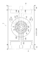
[波長可変干渉フィルターの構成]
光学モジュール10の波長可変干渉フィルター5について、以下説明する。図3は、波長可変干渉フィルター5の概略構成を示す平面図である。図4は、固定基板51を可動基板52側から見た平面図である。図5は、可動基板52を固定基板51側から見た平面図である。なお、図3において、固定基板51に設けられる膜(固定反射膜54,第一電極561A,第三電極562A,第一引出電極563A,第三引出電極564A,第五引出電極565A)を実線で示し、可動基板52に設けられる膜(可動反射膜55,第二電極561B,第四電極562B,第二引出電極563B,第四引出電極564B,第六引出電極565B)を破線で示す。
波長可変干渉フィルター5は、図3に示すように、例えば矩形板状の光学部材であり、固定基板51および可動基板52を備えている。これらの固定基板51及び可動基板52は、それぞれ各種ガラスや水晶等により形成され、固定基板51の第一接合部513及び可動基板の第二接合部523が、例えばシロキサンを主成分とするプラズマ重合膜などにより構成された接合膜53(図2参照)により接合されることで、一体的に構成されている。
[Configuration of wavelength tunable interference filter]
The wavelength
As shown in FIG. 3, the wavelength
固定基板51には、本発明の一方の反射膜を構成する固定反射膜54が設けられ、可動基板52には、本発明の他方の反射膜を構成する可動反射膜55が設けられている。これらの固定反射膜54および可動反射膜55は、反射膜間ギャップG1(図2参照)を介して対向配置されている。そして、波長可変干渉フィルター5には、この反射膜間ギャップG1のギャップ量を調整(変更)するのに用いられる静電アクチュエーター部56が設けられている。この静電アクチュエーター部56は、それぞれ独立して駆動可能な第一静電アクチュエーター561と第二静電アクチュエーター562とを備えている。
なお、以降の説明に当たり、固定基板51または可動基板52の基板厚み方向から見た平面視、つまり、固定基板51、接合膜53、及び可動基板52の積層方向から波長可変干渉フィルター5を見た平面視を、フィルター平面視と称する。また、本実施形態では、フィルター平面視において、固定反射膜54の中心点及び可動反射膜55の中心点は、一致し、平面視におけるこれらの反射膜の中心点をフィルター中心点Oと称し、これらの反射膜の中心点を通る直線を中心軸と称する。
The fixed
In the following description, the wavelength
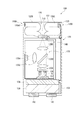
(固定基板の構成)
固定基板51は、可動基板52に対して厚み寸法が大きく形成されており、静電アクチュエーター部56による静電引力や、固定基板51上に形成される膜部材(例えば固定反射膜54等)の内部応力による固定基板51の撓みはない。
この固定基板51は、図4に示すように、例えばエッチング等により形成された電極配置溝511および反射膜設置部512を備える。また、固定基板51の一端側(図3、図4における辺C1−C2)は、可動基板52の基板端縁(図3、図4における辺C5−C6)よりも外側に突出しており、固定側端子取出し部514を構成している。
(Configuration of fixed substrate)
The fixed
As shown in FIG. 4, the fixed
電極配置溝511は、フィルター平面視で、固定基板51のフィルター中心点Oを中心とした環状に形成されている。反射膜設置部512は、フィルター平面視において、電極配置溝511の中心部から可動基板52側に突出して形成されている。この電極配置溝511の溝底面は、静電アクチュエーター部56の電極が配置される電極設置面511Aとなる。また、反射膜設置部512の突出先端面は、反射膜設置面512Aとなる。
また、固定基板51には、電極配置溝511から、固定基板51の外周縁に向かって延出する電極引出溝511Bが設けられている。具体的には、電極引出溝511Bは、辺C3−C4に向かう3つ電極引出溝511Bと、辺C1−C2に向かい、固定側端子取出し部514に繋がる3つの電極引出溝511Bと、を備える。
The
The fixed
電極配置溝511の電極設置面511Aには、第一静電アクチュエーター561を構成する第一電極561A、及び第二静電アクチュエーター562を構成する第三電極562Aが設けられている。より具体的には、これらの第一電極561A及び第三電極562Aは、電極設置面511Aのうち、後述する可動部521に対向する領域に設けられている。また、第一電極561Aは、反射膜設置部512の外周側で第三電極562Aの内周側に設けられ、第三電極562Aは、第一電極561Aの外周側に設けられる。これらの第一電極561A及び第三電極562Aは、それぞれ円弧状(略C字状)に形成されており、辺C1−C2に近接する一部にC字開口部が設けられる。また、第一電極561A及び第三電極562A上に、第二電極561B及び第四電極562Bとの間の絶縁性を確保するための絶縁膜が積層される構成としてもよい。
そして、固定基板51には、図4に示すように、第一電極561Aの一端部から頂点C2に向かって延出する第一引出電極563Aが設けられ、第三電極562Aの一端部から頂点C1に向かって延出する第三引出電極564Aが設けられている。第一引出電極563Aは、頂点C2に向かって延出する電極引出溝511Bに沿って配置され、固定側端子取出し部514上の頂点C2まで延出する。また、第三引出電極564Aは、頂点C1に向かって延出する電極引出溝511Bに沿って配置され、固定側端子取出し部514上の頂点C1まで延出する。そして、これらの第一引出電極563A及び第三引出電極564Aの延出先端部は、例えばFPC(Flexible printed circuits)やリード線等により電圧制御部15に接続されている。
A
As shown in FIG. 4, the fixed
反射膜設置部512は、上述したように、電極配置溝511と同軸上で、電極配置溝511よりも小さい径寸法となる略円柱状に形成され、当該反射膜設置部512の可動基板52に対向する反射膜設置面512Aを備えている。
この反射膜設置部512には、図4に示すように、固定反射膜54が設置されている。この固定反射膜54としては、例えばAg等の金属膜や、Ag合金等、導電性の合金膜を用いることができる。また、例えば高屈折層をTiO2、低屈折層をSiO2とした誘電体多層膜を用いてもよく、この場合、誘電体多層膜の最下層又は表層に導電性の金属合金膜が形成されていることが好ましい。
そして、固定基板51には、図4に示すように、固定反射膜54の外周縁から延出する第五引出電極565Aが設けられる。この第五引出電極565Aは、例えば、第一引出電極563A及び第三引出電極564Aの間を通り、辺C1−C2の中点に向かって延出する電極引出溝511Bに沿って配置され、固定側端子取出し部514上の辺C1−C2の中点位置まで延出する。そして、第一引出電極563A,第四引出電極564Bと同様に、第五引出電極565Aの延出先端部は、例えばFPCやリード線等により電圧制御部15に接続されている。
As described above, the reflective
As shown in FIG. 4, a fixed
As shown in FIG. 4, the fixed
また、固定基板51の光入射面(固定反射膜54が設けられない面)には、固定反射膜54に対応する位置に反射防止膜を形成してもよい。この反射防止膜は、低屈折率膜および高屈折率膜を交互に積層することで形成することができ、固定基板51の表面での可視光の反射率を低下させ、透過率を増大させる。
Further, an antireflection film may be formed at a position corresponding to the fixed
そして、固定基板51の可動基板52に対向する面のうち、電極配置溝511、反射膜設置部512、及び電極引出溝511Bが形成されない面は、第一接合部513を構成する。この第一接合部513は、接合膜53により、可動基板52の第二接合部523に接合される。
Of the surfaces of the fixed
(可動基板の構成)
可動基板52は、図3に示すようなフィルター平面視において、フィルター中心点Oを中心とした円形状の可動部521と、可動部521と同軸であり可動部521を保持する保持部522と、保持部522の外側に設けられた基板外周部525と、を備えている。
また、可動基板52には、図3に示すように、一端側(図3、図5における辺C7−C8)は、固定基板51の基板端縁(図3、図4における辺C3−C4)よりも外側に突出しており、可動側端子取出し部524を構成している。
(Configuration of movable substrate)
The
Further, as shown in FIG. 3, the
可動部521は、保持部522よりも厚み寸法が大きく形成され、例えば、本実施形態では、可動基板52の厚み寸法と同一寸法に形成されている。この可動部521は、フィルター平面視において、少なくとも反射膜設置面512Aの外周縁の径寸法よりも大きい径寸法に形成されている。そして、この可動部521には、可動反射膜55、第一静電アクチュエーター561を構成する第二電極561B、及び第二静電アクチュエーター562を構成する第四電極562Bが設けられている。
なお、固定基板51と同様に、可動部521の固定基板51とは反対側の面には、反射防止膜が形成されていてもよい。
The
Similar to the fixed
第二電極561Bは、可動反射膜55の外周側に設けられ、第四電極562Bは、第二電極561Bの外周側に設けられている。これらの第二電極561B及び第四電極562Bは、それぞれ円弧状(略C字状)に形成されており、辺C7−C8に近接する一部にC字開口部が設けられる。ここで、フィルター平面視において、第二電極561Bは、第一電極561Aと重なる円弧領域を備え、この円弧領域により、第一静電アクチュエーター561が構成される。同様に、第四電極562Bは、第二電極561Bと重なる円弧領域を備え、この円弧領域により、第二静電アクチュエーター562が構成される。
なお、第一電極561A及び第三電極562Aと同様に、第二電極561B及び第四電極562B上に、絶縁性を確保するための絶縁膜が積層される構成としてもよい。
The
Note that, similarly to the
また、可動基板52には、図5に示すように、第二電極561Bの一端部から頂点C8に向かって延出する第二引出電極563Bが設けられ、第四電極562Bの一端部から頂点C7に向かって延出する第四引出電極564Bが設けられている。第二引出電極563Bは、固定基板51に設けられた頂点C4に向かって延出する電極引出溝511Bに対向する位置に配置され、可動側端子取出し部524上の頂点C8まで延出する。また、第四引出電極564Bは、頂点C3に向かって延出する電極引出溝511Bに対向する位置に配置され、可動側端子取出し部524上の頂点C7まで延出する。そして、これらの第二引出電極563B及び第四引出電極564Bの延出先端部は、例えばFPCやリード線等により電圧制御部15に接続されている。
Further, as shown in FIG. 5, the
可動反射膜55は、可動部521の可動面521Aの中心部に、固定反射膜54と反射膜間ギャップG1を介して対向して設けられる。この可動反射膜55としては、上述した固定反射膜54と同一の構成の反射膜が用いられる。
また、可動基板52には、図5に示すように、可動反射膜55の外周縁から延出する第六引出電極565Bが設けられる。この第六引出電極565Bは、例えば、第二引出電極563B及び第四引出電極564Bの間を通り、固定基板51の辺C3−C4の中点に向かって延出する電極引出溝511Bに対向する位置に配置され、可動側端子取出し部524上の辺C7−C8の中点位置まで延出する。そして、第二引出電極563B,第四引出電極564Bと同様に、第六引出電極565Bの延出先端部は、例えばFPCやリード線等により電圧制御部15に接続されている。
The movable
Further, as shown in FIG. 5, the
なお、本実施形態では、上述したように、電極間ギャップG2(図2参照)のギャップ量が反射膜間ギャップG1のギャップ量よりも大きい例を示すがこれに限定されない。例えば、測定対象光として赤外線や遠赤外線を用いる場合等、測定対象光の波長域によっては、反射膜間ギャップG1のギャップ量が、電極間ギャップG2のギャップ量よりも大きくなる構成としてもよい。 In the present embodiment, as described above, an example in which the gap amount of the interelectrode gap G2 (see FIG. 2) is larger than the gap amount of the inter-reflection film gap G1 is shown, but the present invention is not limited to this. For example, when using infrared rays or far infrared rays as the measurement target light, the gap amount of the reflection film gap G1 may be larger than the gap amount of the interelectrode gap G2 depending on the wavelength range of the measurement target light.
保持部522は、可動部521の周囲を囲うダイヤフラムであり、可動部521よりも厚み寸法が小さく形成されている。このような保持部522は、可動部521よりも撓みやすく、僅かな静電引力により、可動部521を固定基板51側に変位させることが可能となる。この際、可動部521が保持部522よりも厚み寸法が大きく、剛性が大きくなるため、保持部522が静電引力により固定基板51側に引っ張られた場合でも、可動部521の形状変化が起こらない。したがって、可動部521に設けられた可動反射膜55の撓みも生じず、固定反射膜54及び可動反射膜55を常に平行状態に維持することが可能となる。
なお、本実施形態では、ダイヤフラム状の保持部522を例示するが、これに限定されず、例えば、フィルター中心点Oを中心として、等角度間隔で配置された梁状の保持部が設けられる構成などとしてもよい。
The holding
In this embodiment, the diaphragm-
基板外周部525は、上述したように、フィルター平面視において保持部522の外側に設けられている。この基板外周部525の固定基板51に対向する面には、第一接合部513に対向する第二接合部523が設けられ、接合膜53を介して第一接合部513に接合される。
As described above, the substrate outer
[電圧制御部の構成]
電圧制御部15は、図2に示すように、バイアス駆動部151(バイアス電圧印加手段)と、ギャップ検出器152(ギャップ検出手段)と、フィードバック制御部153(フィードバック電圧印加手段)と、マイコン(マイクロコントローラー)154とを備えて構成されている。
バイアス駆動部151は、波長可変干渉フィルター5の第一引出電極563A及び第二引出電極563Bに接続され、第一静電アクチュエーター561に対してバイアス電圧を印加する。具体的には、バイアス駆動部151は、所定bit数を有するD/A変換器により構成され、マイコン154から入力されたバイアス信号に基づいて、第一静電アクチュエーター561に電圧を印加する。
[Configuration of voltage controller]
As shown in FIG. 2, the
The
ギャップ検出器152は、波長可変干渉フィルター5の第五引出電極565A及び第六引出電極565Bに接続され、反射膜間ギャップG1のギャップ量に応じた検出信号を取得する。また、ギャップ検出器152は、取得した検出信号をフィードバック制御部153に出力する。
フィードバック制御部153は、波長可変干渉フィルター5の第三引出電極564A及び第四引出電極564Bに接続され、第二静電アクチュエーター562に対してフィードバック電圧を印加する。この際、フィードバック制御部153は、ギャップ検出器152から入力される検出信号と、マイコン154から入力される目標値(目標検出信号)とが同値となるように、第二静電アクチュエーター562に対してフィードバック電圧を印加する。
また、本実施形態のフィードバック制御部153は、固定ゲインを有するアナログ制御器により構成され、電圧可変範囲が所定幅に設定されている。このようなアナログ制御器は、例えば可変ゲインを有するアナログ制御器よりも簡素なシステム構成で組み込むことができ、低コスト化を図ることができる。ここで、アナログ制御器として、例えばPI制御器やPID制御器などを用いることができる。また、その他の制御器を用いてもよい。
The
The
In addition, the
マイコン154は、制御部20、バイアス駆動部151、ギャップ検出器152、及びフィードバック制御部153に接続されている。また、マイコン154は、メモリー等により構成される記憶手段(図示略)を備えている。この記憶手段には、例えば反射膜間ギャップG1のギャップ量に対する、ギャップ検出器152で検出される検出信号(電圧信号)であるギャップ相関データが記憶されている。
そして、マイコン154は、制御部20から入力される制御信号に基づいて、バイアス駆動部151、ギャップ検出器152、及びフィードバック制御部153を制御し、波長可変干渉フィルター5から目的波長の光を透過させる。
なお、電圧制御部15による波長可変干渉フィルター5の駆動電圧の制御についての詳細な説明は後述する。
[制御部の構成]
図1に戻り、分光測定装置1の制御部20について、説明する。
制御部20は、本発明の処理部に相当し、例えばCPUやメモリー等が組み合わされることで構成され、分光測定装置1の全体動作を制御する。この制御部20は、図1に示すように、波長設定部21と、光量取得部22と、分光測定部23と、を備えている。
The microcomputer 154 is connected to the
The microcomputer 154 controls the
A detailed description of the control of the driving voltage of the wavelength
[Configuration of control unit]
Returning to FIG. 1, the
The
波長設定部21は、波長可変干渉フィルター5により取り出す光の目的波長を設定し、設定した目的波長を波長可変干渉フィルター5から取り出す旨の制御信号を電圧制御部15に出力する。
光量取得部22は、ディテクター11により取得された光量に基づいて、波長可変干渉フィルター5を透過した目的波長の光の光量を取得する。
分光測定部23は、光量取得部22により取得された光量に基づいて、測定対象光のスペクトル特性を測定する。
The wavelength setting unit 21 sets a target wavelength of light extracted by the wavelength
The light quantity acquisition unit 22 acquires the light quantity of the target wavelength light transmitted through the wavelength
The
[波長可変干渉フィルターの駆動方法]
図6は、分光測定装置1の分光測定処理における波長可変干渉フィルターの駆動方法(駆動処理)を示すフローチャートである。
分光測定装置1により測定対象光に含まれる各波長の光の強度を取得するためには、まず、制御部20は、波長設定部21により波長可変干渉フィルター5を透過させる光の波長(目的波長)を設定する。そして、波長設定部21は、設定した目的波長の光を透過させる旨の制御信号を電圧制御部15に出力する(S1)。
[Driving method of tunable interference filter]
FIG. 6 is a flowchart showing a driving method (driving process) of the variable wavelength interference filter in the spectroscopic measurement process of the
In order to acquire the intensity of light of each wavelength included in the measurement target light by the
電圧制御部15のマイコン154は、制御部20から制御信号が入力されると、目的波長に対応したバイアス電圧を算出する(S2)。
ここで、本実施形態では、マイコン154は、後述のフィードバック制御において、第二静電アクチュエーター562への電圧印加時の感度(印加電圧に対するギャップ変位量(m/V))が一定となるように、バイアス電圧を設定する。
ここで、第二静電アクチュエーター562への電圧印加時の感度RC(m/V)は、次式(2)により表される。
When the control signal is input from the
Here, in the present embodiment, the microcomputer 154 makes the sensitivity (gap displacement amount (m / V) with respect to the applied voltage) constant when the voltage is applied to the second
Here, the sensitivity R C (m / V) when a voltage is applied to the second
図7は、上記式(2)を説明するための図であり、静電アクチュエーター部56の等価回路モデルである。
図7及び式(2)において、Vbは、第一静電アクチュエーター561に印加するバイアス電圧、kは、可動基板52(保持部522)のバネ係数、εは、固定基板51及び可動基板52間(電極間ギャップG2)の誘電率、Sbは、第一電極561A及び第二電極561Bにおいて、フィルター平面視で互いに重なり合う領域(第一静電アクチュエーター561として機能する領域)の面積、SCは、第三電極562A及び第四電極562Bにおいて、フィルター平面視で互いに重なり合う領域(第二静電アクチュエーター562として機能する領域)の面積、dmaxは電極間ギャップG2の初期ギャップ量(電圧を印加していない状態でのギャップ量)、dは、目的波長の光を透過させるための可動部521の変位量(電極間ギャップG2のギャップ変位量)である。また、図7において、bは、ダンピング係数を示している。
FIG. 7 is a diagram for explaining the above equation (2), and is an equivalent circuit model of the
7 and Expression (2), V b is a bias voltage applied to the first
本実施形態では、フィードバック制御時において、第二静電アクチュエーター562への電圧印加時の感度が一定になるようにバイアス電圧Vbを印加する。すなわち、上記式(2)において、RCは、一定値であり、フィードバック制御部153のアナログ制御器における固定ゲインに応じた予め設定された値が用いられる。また、制御部20から、目的波長を指定する制御信号が入力されれば、マイコン154は、波長可変干渉フィルター5から目的波長の光を取り出すために必要な反射膜間ギャップG1の目標ギャップ量を算出することができ、目標ギャップ量から、可動部521を変位させるべき量(目標変位量d)を算出することができる。
上記式(2)を、Vbについて解くと、上述した式(1)を導き出すことができる。したがって、S2では、マイコン154は、式(1)に基づいて、フィードバック制御において、所定の感度で第二静電アクチュエーター562を駆動させるために必要となる第一静電アクチュエーター561への印加電圧(バイアス電圧)を算出する。
In the present embodiment, during feedback control, the bias voltage Vb is applied so that the sensitivity at the time of voltage application to the second
When the above equation (2) is solved for V b , the above equation (1) can be derived. Therefore, in S2, the microcomputer 154 applies the voltage applied to the first
そして、マイコン154は、S2により算出されたバイアス電圧に基づいたバイアス信号をバイアス駆動部151に出力する。これにより、バイアス駆動部151は、S2により算出されたバイアス電圧を、第一静電アクチュエーター561に対して印加する(S3:バイアス電圧印加ステップ)。このS3により、第一電極561A及び第二電極561B間に、バイアス電圧に基づいた静電引力が作用し、可動部521が固定基板51側に変位する。
Then, the microcomputer 154 outputs a bias signal based on the bias voltage calculated in S2 to the
ここで、図8に、フィードバック制御時において、第一静電アクチュエーター561に印加するバイアス電圧を印加した際の第二静電アクチュエーター562の感度を説明するための図を示す。
図8(A)の破線で示すように、フィードバック電圧を印加する第二静電アクチュエーター562の感度は、第一静電アクチュエーター561にバイアス電圧を印加しない状態では、変位量に対して感度が大きく変化し、変位量が大きくなるに従って感度が高くなる。このようにフィードバック電圧を印加する静電アクチュエーターの感度が変化する場合、ある特定の感度にあわせてアナログ制御器のゲインを設定しても、変位量が異なるところでは感度が大きく異なり、アナログ制御器が適切に機能しない。つまり、バイアス電圧を印加しない状態では、ゲインを設定したギャップの近傍でしかアナログ制御器は適切に機能しないことになる。
本実施形態では図8(B)に示すように第一静電アクチュエーター561に式(1)に基づいたバイアス電圧を印加することで、図8(A)の実線で示すように、第二静電アクチュエーター562の感度は所望の感度RC1で一定となる。
尚、本実施例では、感度RCが一定となるようなバイアス電圧を印加する例について示したが、バイアス電圧の値は式(1)に基づいた値に限らず、所望の感度特性となるようにバイアス電圧を印加しても良い。
Here, FIG. 8 shows a diagram for explaining the sensitivity of the second
As shown by a broken line in FIG. 8A, the sensitivity of the second
In this embodiment, as shown in FIG. 8B, by applying a bias voltage based on the formula (1) to the first
In this embodiment, an example in which a bias voltage is applied so that the sensitivity RC is constant has been described. However, the value of the bias voltage is not limited to the value based on the expression (1), and a desired sensitivity characteristic is obtained. Thus, a bias voltage may be applied.
この後、フィードバック制御部153によりフィードバック制御を実施する(S4)。このフィードバック制御(S4)には、本発明のギャップ検出ステップと、フィードバック電圧印加ステップとが含まれる。
すなわち、マイコン154は、ギャップ検出器152から静電容量検出用の高周波電圧を固定反射膜54,可動反射膜55に印加させる。これにより、ギャップ検出器152により、固定反射膜54及び可動反射膜55の静電容量に応じた検出信号を取得することができ、取得された検出信号は、フィードバック制御部153に出力される(ギャップ検出ステップ)。
また、マイコン154は、制御部20からの制御信号に基づいて、目的波長に対応する目標ギャップ量を算出するとともに、記憶手段に記憶されたギャップ相関データから、目標ギャップ量に対応した検出信号(目標検出信号)を取得し、フィードバック制御部153に出力する。
そして、フィードバック制御部153は、マイコン154から入力される目標検出信号と、ギャップ検出器152から入力される検出信号との差を算出し、その差が「0」となるように、第二静電アクチュエーター562に対してフィードバック電圧を印加する(フィードバック電圧印加ステップ)。
Thereafter, feedback control is performed by the feedback control unit 153 (S4). This feedback control (S4) includes a gap detection step and a feedback voltage application step of the present invention.
That is, the microcomputer 154 causes the
Further, the microcomputer 154 calculates a target gap amount corresponding to the target wavelength based on the control signal from the
Then, the
ここで、図9に、フィードバック制御の概念図を示す。
図9に示すように、バイアス駆動部151は、図8に示したような、第二静電アクチュエーター562の感度が一定にするバイアス電圧を第一静電アクチュエーター561に印加している。
したがって、フィードバック電圧印加ステップでは、フィードバック電圧印可部153のアナログ制御器は、マイコン154から入力された目標値信号とギャップ検出器から出力される信号の偏差に基づいて、偏差が0となるように第二静電アクチュエーター562に印加するフィードバック電圧を設定すればよい。
この場合、可動部521の変位量(電極間ギャップG2の変化量)によらず、低い感度で第二静電アクチュエーター562を駆動させることが可能となる。
Here, FIG. 9 shows a conceptual diagram of feedback control.
As shown in FIG. 9, the
Therefore, in the feedback voltage applying step, the analog controller of the feedback
In this case, the second
そして、S4の後、波長可変干渉フィルター5を透過した光をディテクター11により検出し(S5)、制御部20の波長設定部21により、透過した波長の光の光量を取得する。
なお、上記において、1つ波長の光を波長可変干渉フィルター5から取り出し、その光量を検出する処理について、説明したが、例えば測定対象光に含まれる所定波長域内の各波長に対する光量から測定対象光の分光スペクトルを測定する場合、S1において設定する波長を順次変更して、上記S2〜S5処理を繰り返せばよい。
Then, after S4, the light transmitted through the variable
In the above description, the process of taking out light of one wavelength from the wavelength
[本実施形態の作用効果]
本実施形態の分光測定装置1の光学モジュール10は、波長可変干渉フィルター5及び電圧制御部15を備えている。波長可変干渉フィルター5は、固定反射膜54及び可動反射膜55間の反射膜間ギャップG1を変更するための静電アクチュエーター部56を備え、この静電アクチュエーター部56は、第一静電アクチュエーター561及び第二静電アクチュエーター562を備えている。また、電圧制御部15は、バイアス駆動部151、ギャップ検出器152、フィードバック制御部153、及びマイコン154を備えている。そして、マイコン154は、制御部20から入力された制御信号(目的波長)に基づいて、バイアス駆動部151にバイアス信号を出力し、フィードバック制御部153に目的波長に対応した目標検出信号を出力する。これにより、バイアス駆動部151は、第一静電アクチュエーター561にバイアス電圧を印加して、可動部521を目標変位量近傍まで移動させる。また、フィードバック制御部153は、ギャップ検出器152からの検出信号と、目標検出信号との差が「0」となるように、第二静電アクチュエーター562にフィードバック電圧を印加する。
このような構成では、フィードバック制御部153により第二静電アクチュエーター562にフィードバック電圧を印加して、反射膜間ギャップG1のギャップ量を微調整する際に、第二静電アクチュエーター562の感度を低減させることができる。すなわち、反射膜間ギャップG1の目標ギャップ量によらず、第二静電アクチュエーター562の感度を低減できる。したがって、フィードバック制御部153のアナログ制御器のゲインを一定ゲインに固定したまま、反射膜間ギャップG1の広いギャップ範囲に対して、フィードバック制御による高精度なギャップ量の微調整を実施することができる。また、フィードバック制御部153として、複雑なシステム構成が必要となる可変ゲインを有するアナログ制御器が不要となり、構成の簡略化、低コスト化を図ることができる。
[Operational effects of this embodiment]
The
In such a configuration, when the
本実施形態の光学モジュール10は、バイアス駆動部151は、上記式(1)に基づいたバイアス電圧を第一静電アクチュエーター561に印加する。このため、反射膜間ギャップG1のギャップ量によらず、フィードバック制御における第二静電アクチュエーター562の感度を一定にできる。したがって、フィードバック制御部153におけるフィードバック電圧の設定が容易となり、より高精度なフィードバック制御を行うことができる。
また、マイコン154は、上記式(1)に基づいて、バイアス電圧を算出して、バイアス信号をバイアス駆動部151に出力する。このため、例えば、反射膜間ギャップG1の目標ギャップ量に対するバイアス電圧をテーブルデータとして記憶する場合に比べて、より正確なバイアス電圧を設定することができ、データを保持するための大容量の記憶領域が不要となるので低コスト化を図ることもできる。
In the
Further, the microcomputer 154 calculates a bias voltage based on the above formula (1), and outputs a bias signal to the
本実施形態では、フィードバック制御部153は、アナログ制御器を備え、フィードバック電圧としてアナログ電圧を第二静電アクチュエーター562に印加する。ここで、本実施形態では、上述したように、バイアス電圧を第一静電アクチュエーター561に印加することで、第二静電アクチュエーター562の感度を一定にすることができるため、アナログ制御器のゲインを1つに固定することができ、フィードバック制御部153の構成の簡略化を図ることができる。
In the present embodiment, the
本実施形態の波長可変干渉フィルター5では、固定反射膜54及び可動反射膜55が、本発明の第一静電容量検出電極及び第二静電容量検出電極として機能し、フィードバック制御部153は、固定反射膜54及び可動反射膜55の間の静電容量に基づいて、反射膜間ギャップG1のギャップ量に基づいた検出信号を検出する。
このような構成では、固定基板51及び可動基板52に設けられた固定反射膜54及び可動反射膜55により、容易に反射膜間ギャップG1のギャップ量を検出することができ、波長可変干渉フィルター5の構成の簡略化を図ることができる。また、固定反射膜54及び可動反射膜55の間の静電容量を検出するため、静電容量検出用の専用の別電極が不要となる。この点からも、波長可変干渉フィルター5の構成の簡略化が図れる。
In the wavelength
In such a configuration, the fixed
本実施形態では、第一静電アクチュエーター561を構成する第一電極561A及び第二電極561Bは、それぞれ、固定反射膜54及び可動反射膜55の外周側に設けられている。また、第二静電アクチュエーター562を構成する第三電極562A及び第四電極562Bは、それぞれ、第一電極561A及び第二電極561Bの更に外側に設けられている。
すなわち、高い周波数成分を含む可能性があるフィードバック電圧が印加される第二静電アクチュエーター562は、反射膜間ギャップG1のギャップ量を検出するための固定反射膜54及び可動反射膜55から離れた位置に配置されている。これにより、第二静電アクチュエーター562から固定反射膜54及び可動反射膜55へのクロストークを抑制でき、ギャップ検出器152において、精度よく反射膜間ギャップG1のギャップ量を検出することができる。
In the present embodiment, the
That is, the second
[第二実施形態]
上記第一実施形態では、固定ゲインを有するアナログ制御器を備えたフィードバック制御部153を例示した。これに対して、第二実施形態では、フィードバック制御部153が第二静電アクチュエーター562に対してデジタル制御器により出力される電圧(本発明のデジタル電圧)を印加する点で、上記第一実施形態と相違する。
なお、第二実施形態は、上記第一実施形態と同様の構成を有するものであるため、図1に基づいて、以下第二実施形態のフィードバック制御部153について説明し、その他の構成については、その説明を省略する。
[Second Embodiment]
In the first embodiment, the
Since the second embodiment has the same configuration as the first embodiment, the
本実施形態のフィードバック制御部153は、ギャップ検出器152から入力される電圧をデジタル信号(検出信号)へ変換するA/D変換器と、検出信号と目標検出信号との差に基づいてフィードバック電圧値を算出する演算器と、演算結果のフィードバック電圧値のデジタル信号をアナログ電圧へ変換し、第二静電アクチュエーター562に対して電圧を印加するD/A変換器と、により構成されている。そして、このフィードバック制御部153は、第一実施形態と同様に、マイコン154から入力される目標検出信号と、フィードバック制御部153から入力される検出信号との差に基づいて、当該差が「0」となるように、第二静電アクチュエーター562に対してフィードバック電圧を設定して印加する。
The
このように、フィードバック制御部153のD/A変換器により第二静電アクチュエーター562に電圧を印加する場合、第二静電アクチュエーター562の感度変化に合わせてデジタル信号処理で適切なフィードバック電圧値を算出するため、回路のゲイン調整が不要であり、D/A変換器により設定する電圧を所望の値に設定することで、高精度なフィードバック制御を行うことができる。しかしながら、バイアス駆動部151により、バイアス電圧をバイアス駆動部151に印加しない構成では、フィードバック制御を実施する際に、電極間ギャップG2のギャップ量が小さくなるに従って、フィードバック電圧を印加する静電アクチュエーターの感度が増加する。したがって、高精度なフィードバック制御を実施するために、フィードバック制御部153は、入力電圧を細かく分割して、第二静電アクチュエーターに562印加する必要がある。つまり、フィードバック制御部153としてbit数が大きいD/A変換器を用いる必要が生じ、コストが高くなる。
これに対して、本実施形態では、上記第一実施形態と同様に、バイアス電圧を、バイアス駆動部151から第一静電アクチュエーター561に印加することで、バイアス電圧を印加しない場合に比べて、第二静電アクチュエーター562の感度を低くすることができる。これにより、フィードバック制御部153により設定するフィードバック電圧として、バイアス電圧を印加しない場合に比べて、電圧の分解能を小さくできる。したがって、フィードバック制御部153には、bit数が小さいD/A変換器が設けられていればよく、フィードバック制御部153の低コスト化を図ることができる。
As described above, when a voltage is applied to the second
On the other hand, in the present embodiment, as in the first embodiment, by applying a bias voltage from the
[第三実施形態]
上記第一及び第二実施形態では、固定反射膜54及び可動反射膜55が本発明の第一静電容量検出電極及び第二静電容量検出電極を構成する例を示した。これに対して、第三実施形態では、第一静電容量検出電極及び第二静電容量検出電極を構成する電極が異なる点で、上記第一実施形態と相違する。
[Third embodiment]
In the first and second embodiments, the example in which the fixed
図10は、第三実施形態における波長可変干渉フィルター5Aの概略構成を示す平面図である。
図10に示すように、本実施形態の波長可変干渉フィルター5Aでは、第一静電アクチュエーター561を構成する第一電極561A及び第二電極561Bが、本発明の第一静電容量検出電極及び第二静電容量検出電極を構成する。この場合、第一引出電極563A及び第二引出電極563Bは、バイアス駆動部151及びギャップ検出器152に接続される。
本実施形態では、第一静電アクチュエーター561に対して、ギャップ検出器152から出力される静電容量検出用の電圧信号と、バイアス駆動部151から出力されるバイアス電圧とが印加されることになる。この場合、静電容量検出用の電圧信号を、静電アクチュエーター部56の駆動に影響しない程度に十分に高周波となる信号を用いる。また、ギャップ検出器152では、例えばカップリングコンデンサー等を用いて2信号を分離し、静電容量検出用の電圧信号を検出する。これにより、静電容量検出用の電圧信号によるギャップ変動への影響を防止でき、上記第一実施形態と同様に、高精度な反射膜間ギャップG1のギャップ量制御を実施することができる。また、本実施形態では、固定反射膜54に接続される第五引出電極565A、及び可動反射膜55に接続される第六引出電極565Bが不要となるため、波長可変干渉フィルター5Aの電極構造を簡略化できる。
なお、上記例では、第一静電アクチュエーター561の第一電極561A及び第二電極561Bを、本発明の第一静電容量検出電極及び第二静電容量検出電極として機能させたが、第二静電アクチュエーター562の第三電極562A及び第四電極562Bを、本発明の第一静電容量検出電極及び第二静電容量検出電極として機能させてもよい。この場合では、第三引出電極564A及び第四引出電極564Bを、ギャップ検出器152及びフィードバック制御部153に接続すればよい。
FIG. 10 is a plan view showing a schematic configuration of the variable
As shown in FIG. 10, in the variable
In the present embodiment, a voltage signal for capacitance detection output from the
In the above example, the
[その他の実施形態]
なお、本発明は前述の実施形態に限定されるものではなく、本発明の目的を達成できる範囲での変形、改良等は本発明に含まれるものである。
[Other Embodiments]
It should be noted that the present invention is not limited to the above-described embodiments, and modifications, improvements, and the like within the scope that can achieve the object of the present invention are included in the present invention.
例えば、本発明の第一静電容量検出電極及び第二静電容量検出電極として、第一及び第二実施形態では、固定反射膜54及び可動反射膜55を用い、第三実施形態では、第一静電アクチュエーター561の第一電極561A及び第二電極561B、又は、第二静電アクチュエーター562の第三電極562A及び第四電極562Bを用いる例を示したが、これに限られない。
固定基板51及び可動基板52に、本発明の第一静電容量検出電極及び第二静電容量検出電極を構成する別の電極を更に設けてもよい。例えば、固定反射膜54及び第三電極562Aの間に、静電容量検出用の第五電極を設け、可動反射膜55及び第四電極562Bの間に、第五電極に対向する第六電極を設ける構成とし、第五電極及び第六電極間の静電容量を検出する構成としてもよい。
For example, as the first capacitance detection electrode and the second capacitance detection electrode of the present invention, in the first and second embodiments, the fixed
Another electrode constituting the first capacitance detection electrode and the second capacitance detection electrode of the present invention may be further provided on the fixed
また、ギャップ検出手段としては、上述のような静電容量検出電極を用いる構成に限られず、例えば、歪ゲージ等により、可動基板52(保持部522)の湾曲状態を検出して、反射膜間ギャップG1のギャップ量を検出する構成としてもよく、外部にギャップ量を検出するための光センサーを設ける構成などとしてもよい。 The gap detection means is not limited to the configuration using the capacitance detection electrode as described above. For example, the bending state of the movable substrate 52 (holding portion 522) is detected by a strain gauge or the like, and the gap between the reflection films is detected. It may be configured to detect the gap amount of the gap G1, or may be configured to provide an optical sensor for detecting the gap amount outside.
また、上記各実施形態では、式(1)に基づいて、バイアス駆動部151に印加するバイアス電圧を設定したが、これに限定されない。例えば、反射膜間ギャップG1の目標ギャップ量に対するバイアス電圧がテーブルデータに記憶され、記憶手段に記憶される構成としてもよい。この場合、マイコン154は、式(1)に基づいたバイアス電圧の算出を実施せず、テーブルデータから目標ギャップ量に対するバイアス電圧を読み出せばよい。
また、バイアス電圧としては、バイアス駆動部151を単独駆動させて反射膜間ギャップG1を目標ギャップ量に設定するための駆動電圧よりも小さい電圧が用いられていればよい。このようなバイアス電圧が印加されることで、フィードバック制御部153による第二静電アクチュエーター562の制御において、バイアス電圧が印加されない場合に比べて感度を低減させることができ、フィードバック制御の精度を向上させることができる。
In each of the above embodiments, the bias voltage applied to the
In addition, as the bias voltage, a voltage smaller than a drive voltage for driving the
また、上記各実施形態では、静電アクチュエーター部56として、第一静電アクチュエーター561及び第二静電アクチュエーター562が設けられ、第二静電アクチュエーター562によるフィードバック制御を高精度に実施するために、第一静電アクチュエーター561にバイアス電圧を印加する構成とした。これに対して、静電アクチュエーター部56が更に複数(3つ以上)の静電アクチュエーターを備えて構成されてもよい。例えば、静電アクチュエーター部56は、フィードバック制御を実施するための制御用静電アクチュエーター(第二静電アクチュエーター)と、フィードバック制御用静電アクチュエーターの感度を低減させるための第一バイアス静電アクチュエーターと、第一バイアス静電アクチュエーターの感度を低減させてギャップ変位精度を向上させる第二バイアス静電アクチュエーターと、を備える構成としてもよい。
つまり、第一静電アクチュエーターが、少なくとも2つ以上の部分アクチュエーター(上記例では、第一バイアス静電アクチュエーター,第二バイアス静電アクチュエーター)に分割されている構成としてもよい。これらの部分アクチュエーターにより第一静電アクチュエーターに印加するバイアス電圧を制御することで、バイアス電圧をより精度よく制御することができ、ノイズ等による駆動電圧変動の影響をより効果的に減退させることができる。
また、バイアス電圧の電圧分解能を低減させることができるので、バイアス駆動部151のbit数を低減させることができ、更なる低コスト化を図ることができる。
Moreover, in each said embodiment, as the
That is, the first electrostatic actuator may be divided into at least two or more partial actuators (in the above example, the first bias electrostatic actuator and the second bias electrostatic actuator). By controlling the bias voltage applied to the first electrostatic actuator by these partial actuators, the bias voltage can be controlled more accurately, and the influence of drive voltage fluctuations due to noise or the like can be reduced more effectively. it can.
In addition, since the voltage resolution of the bias voltage can be reduced, the number of bits of the
上記各実施形態において、バイアス電圧が印加される第一静電アクチュエーター561は、フィードバック電圧が印加される第二静電アクチュエーター562の外周側に配置される例を示したが、これに限定されない。例えば、第一静電アクチュエーター561が、反射膜54,55の外周側で、第二静電アクチュエーター562の内周側に設けられ、第二静電アクチュエーター562が第一静電アクチュエーター561の外周側に設けられる構成などとしてもよい。
In the above embodiments, the first
また、本発明の電子機器として、上記各実施形態では、分光測定装置1を例示したが、その他、様々な分野により本発明の波長可変干渉フィルターの駆動方法、光学モジュール、及び電子機器を適用することができる。
Moreover, although the
例えば、図11に示すように、本発明の電子機器を、色を測定するための測色装置に適用することもできる。
図11は、波長可変干渉フィルターを備えた測色装置400の一例を示すブロック図である。
この測色装置400は、図11に示すように、検査対象Aに光を射出する光源装置410と、測色センサー420(光学モジュール)と、測色装置400の全体動作を制御する制御装置430(処理部)とを備える。そして、この測色装置400は、光源装置410から射出される光を検査対象Aにて反射させ、反射された検査対象光を測色センサー420にて受光し、測色センサー420から出力される検出信号に基づいて、検査対象光の色度、すなわち検査対象Aの色を分析して測定する装置である。
For example, as shown in FIG. 11, the electronic apparatus of the present invention can also be applied to a color measuring device for measuring color.
FIG. 11 is a block diagram illustrating an example of a
As shown in FIG. 11, the
光源装置410、光源411、複数のレンズ412(図11には1つのみ記載)を備え、検査対象Aに対して例えば基準光(例えば、白色光)を射出する。また、複数のレンズ412には、コリメーターレンズが含まれてもよく、この場合、光源装置410は、光源411から射出された基準光をコリメーターレンズにより平行光とし、図示しない投射レンズから検査対象Aに向かって射出する。なお、本実施形態では、光源装置410を備える測色装置400を例示するが、例えば検査対象Aが液晶パネルなどの発光部材である場合、光源装置400が設けられない構成としてもよい。
A
測色センサー420は、図11に示すように、波長可変干渉フィルター5と、波長可変干渉フィルター5を透過する光を受光するディテクター11と、波長可変干渉フィルター5で透過させる光の波長を可変する電圧制御部15とを備える。また、測色センサー420は、波長可変干渉フィルター5に対向する位置に、検査対象Aで反射された反射光(検査対象光)を、内部に導光する図示しない入射光学レンズを備えている。そして、この測色センサー3は、波長可変干渉フィルター5により、入射光学レンズから入射した検査対象光のうち、所定波長の光を分光し、分光した光をディテクター11にて受光する。なお、波長可変干渉フィルター5に代えて、波長可変干渉フィルター5A,5B,5C,5D,5Eや光学フィルターデバイス600が配置されてもよい。
As shown in FIG. 11, the
制御装置430は、測色装置400の全体動作を制御する。
この制御装置430としては、例えば汎用パーソナルコンピューターや、携帯情報端末、その他、測色専用コンピューターなどを用いることができる。そして、制御装置430は、図11に示すように、光源制御部431、測色センサー制御部432、および測色処理部433などを備えて構成されている。
光源制御部431は、光源装置410に接続され、例えば利用者の設定入力に基づいて、光源装置410に所定の制御信号を出力して、所定の明るさの白色光を射出させる。
測色センサー制御部432は、測色センサー420に接続され、例えば利用者の設定入力に基づいて、測色センサー420にて受光させる光の波長を設定し、この波長の光の受光量を検出する旨の制御信号を測色センサー420に出力する。これにより、測色センサー420の電圧制御部15は、制御信号に基づいて、静電アクチュエーター56に電圧を印加し、波長可変干渉フィルター5を駆動させる。
測色処理部433は、ディテクター11により検出された受光量から、検査対象Aの色度を分析する。
The
As the
The light
The colorimetric
The
また、本発明の電子機器の他の例として、特定物質の存在を検出するための光ベースのシステムが挙げられる。このようなシステムとしては、例えば、本発明の波長可変干渉フィルターを用いた分光計測方式を採用して特定ガスを高感度検出する車載用ガス漏れ検出器や、呼気検査用の光音響希ガス検出器等のガス検出装置を例示できる。
このようなガス検出装置の一例を以下に図面に基づいて説明する。
Another example of the electronic device of the present invention is a light-based system for detecting the presence of a specific substance. As such a system, for example, an in-vehicle gas leak detector that detects a specific gas with high sensitivity by adopting a spectroscopic measurement method using the variable wavelength interference filter of the present invention, or a photoacoustic rare gas detection for a breath test. A gas detection device such as a vessel can be exemplified.
An example of such a gas detection device will be described below with reference to the drawings.
図12は、波長可変干渉フィルターを備えたガス検出装置の一例を示す概略図である。
図13は、図12のガス検出装置の制御系の構成を示すブロック図である。
このガス検出装置100は、図12に示すように、センサーチップ110と、吸引口120A、吸引流路120B、排出流路120C、及び排出口120Dを備えた流路120と、本体部130と、を備えて構成されている。
本体部130は、流路120を着脱可能な開口を有するセンサー部カバー131、排出手段133、筐体134、光学部135、フィルター136、波長可変干渉フィルター5、及び受光素子137(検出部)等を含む検出装置(光学モジュール)と、検出された信号を処理し、検出部を制御する制御部138(処理部)、電力を供給する電力供給部139等から構成されている。また、光学部135は、光を射出する光源135Aと、光源135Aから入射された光をセンサーチップ110側に反射し、センサーチップ側から入射された光を受光素子137側に透過するビームスプリッター135Bと、レンズ135C,135D,135Eと、により構成されている。
また、図13に示すように、ガス検出装置100の表面には、操作パネル140、表示部141、外部とのインターフェイスのための接続部142、電力供給部139が設けられている。電力供給部139が二次電池の場合には、充電のための接続部143を備えてもよい。
更に、ガス検出装置100の制御部138は、図13に示すように、CPU等により構成された信号処理部144、光源135Aを制御するための光源ドライバー回路145、波長可変干渉フィルター5を制御するための電圧制御部146、受光素子137からの信号を受信する受光回路147、センサーチップ110のコードを読み取り、センサーチップ110の有無を検出するセンサーチップ検出器148からの信号を受信するセンサーチップ検出回路149、及び排出手段133を制御する排出ドライバー回路150などを備えている。
FIG. 12 is a schematic diagram illustrating an example of a gas detection device including a wavelength variable interference filter.
FIG. 13 is a block diagram showing a configuration of a control system of the gas detection device of FIG.
As shown in FIG. 12, the
The
As shown in FIG. 13, an
Further, as shown in FIG. 13, the
次に、上記のようなガス検出装置100の動作について、以下に説明する。
本体部130の上部のセンサー部カバー131の内部には、センサーチップ検出器148が設けられており、このセンサーチップ検出器148でセンサーチップ110の有無が検出される。信号処理部144は、センサーチップ検出器148からの検出信号を検出すると、センサーチップ110が装着された状態であると判断し、表示部141へ検出動作を実施可能な旨を表示させる表示信号を出す。
Next, operation | movement of the above
A
そして、例えば利用者により操作パネル140が操作され、操作パネル140から検出処理を開始する旨の指示信号が信号処理部144へ出力されると、まず、信号処理部144は、光源ドライバー回路145に光源作動の信号を出力して光源135Aを作動させる。光源135Aが駆動されると、光源135Aから単一波長で直線偏光の安定したレーザー光が射出される。また、光源135Aには、温度センサーや光量センサーが内蔵されており、その情報が信号処理部144へ出力される。そして、信号処理部144は、光源135Aから入力された温度や光量に基づいて、光源135Aが安定動作していると判断すると、排出ドライバー回路150を制御して排出手段133を作動させる。これにより、検出すべき標的物質(ガス分子)を含んだ気体試料が、吸引口120Aから、吸引流路120B、センサーチップ110内、排出流路120C、排出口120Dへと誘導される。なお、吸引口120Aには、除塵フィルター120A1が設けられ、比較的大きい粉塵や一部の水蒸気などが除去される。
For example, when the
また、センサーチップ110は、金属ナノ構造体が複数組み込まれ、局在表面プラズモン共鳴を利用したセンサーである。このようなセンサーチップ110では、レーザー光により金属ナノ構造体間で増強電場が形成され、この増強電場内にガス分子が入り込むと、分子振動の情報を含んだラマン散乱光、及びレイリー散乱光が発生する。
これらのレイリー散乱光やラマン散乱光は、光学部135を通ってフィルター136に入射し、フィルター136によりレイリー散乱光が分離され、ラマン散乱光が波長可変干渉フィルター5に入射する。そして、信号処理部144は、電圧制御部146に対して制御信号を出力する。これにより、電圧制御部146は、上記第一実施形態に示すように、バイアス駆動部151、ギャップ検出器152、フィードバック制御部153、及びマイコン154により構成され、第一実施形態と同様の駆動方法により、波長可変干渉フィルター5を駆動させ、検出対象となるガス分子に対応したラマン散乱光を波長可変干渉フィルター5で分光させる。この後、分光した光が受光素子137で受光されると、受光量に応じた受光信号が受光回路147を介して信号処理部144に出力される。この場合、波長可変干渉フィルター5から目的とするラマン散乱光を精度よく取り出すことができる。
信号処理部144は、上記のようにして得られた検出対象となるガス分子に対応したラマン散乱光のスペクトルデータと、ROMに格納されているデータとを比較し、目的のガス分子か否かを判定し、物質の特定をする。また、信号処理部144は、表示部141にその結果情報を表示させたり、接続部142から外部へ出力したりする。
The
These Rayleigh scattered light and Raman scattered light enter the
The
なお、上記図12及び図13において、ラマン散乱光を波長可変干渉フィルター5により分光して分光されたラマン散乱光からガス検出を行うガス検出装置100を例示したが、ガス検出装置として、ガス固有の吸光度を検出することでガス種別を特定するガス検出装置として用いてもよい。この場合、センサー内部にガスを流入させ、入射光のうちガスにて吸収された光を検出するガスセンサーを本発明の光学モジュールとして用いる。そして、このようなガスセンサーによりセンサー内に流入されたガスを分析、判別するガス検出装置を本発明の電子機器とする。このような構成でも、波長可変干渉フィルターを用いてガスの成分を検出することができる。
12 and 13 exemplify the
また、特定物質の存在を検出するためのシステムとして、上記のようなガスの検出に限られず、近赤外線分光による糖類の非侵襲的測定装置や、食物や生体、鉱物等の情報の非侵襲的測定装置等の、物質成分分析装置を例示できる。
以下に、上記物質成分分析装置の一例として、食物分析装置を説明する。
In addition, the system for detecting the presence of a specific substance is not limited to the detection of the gas as described above, but a non-invasive measuring device for saccharides by near-infrared spectroscopy, and non-invasive information on food, living body, minerals, etc. A substance component analyzer such as a measuring device can be exemplified.
Hereinafter, a food analyzer will be described as an example of the substance component analyzer.
図14は、波長可変干渉フィルター5を利用した電子機器の一例である食物分析装置の概略構成を示す図である。
この食物分析装置200は、図14に示すように、検出器210(光学モジュール)と、制御部220と、表示部230と、を備えている。検出器210は、光を射出する光源211と、測定対象物からの光が導入される撮像レンズ212と、撮像レンズ212から導入された光を分光する波長可変干渉フィルター5と、分光された光を検出する撮像部213(検出部)と、を備えている。
また、制御部220は、光源211の点灯・消灯制御、点灯時の明るさ制御を実施する光源制御部221と、波長可変干渉フィルター5を制御する電圧制御部222と、撮像部213を制御し、撮像部213で撮像された分光画像を取得する検出制御部223と、信号処理部224(分析部)と、記憶部225と、を備えている。
FIG. 14 is a diagram illustrating a schematic configuration of a food analyzer that is an example of an electronic apparatus using the wavelength
As shown in FIG. 14, the
In addition, the
この食物分析装置200は、システムを駆動させると、光源制御部221により光源211が制御されて、光源211から測定対象物に光が照射される。そして、測定対象物で反射された光は、撮像レンズ212を通って波長可変干渉フィルター5に入射する。波長可変干渉フィルター5は電圧制御部222の制御により、波長可変干渉フィルター5は、上記第一実施形態に示すような駆動方法で駆動される。これにより、波長可変干渉フィルター5から精度よく目的波長の光を取り出すことができる。そして、取り出された光は、例えばCCDカメラ等により構成される撮像部213で撮像される。また、撮像された光は分光画像として、記憶部225に蓄積される。また、信号処理部224は、電圧制御部222を制御して波長可変干渉フィルター5に印加する電圧値を変化させ、各波長に対する分光画像を取得する。
In the
そして、信号処理部224は、記憶部225に蓄積された各画像における各画素のデータを演算処理し、各画素におけるスペクトルを求める。また、記憶部225には、例えばスペクトルに対する食物の成分に関する情報が記憶されており、信号処理部224は、求めたスペクトルのデータを、記憶部225に記憶された食物に関する情報を基に分析し、検出対象に含まれる食物成分、及びその含有量を求める。また、得られた食物成分及び含有量から、食物カロリーや鮮度等をも算出することができる。更に、画像内のスペクトル分布を分析することで、検査対象の食物の中で鮮度が低下している部分の抽出等をも実施することができ、更には、食物内に含まれる異物等の検出をも実施することができる。
そして、信号処理部224は、上述のようにして得られた検査対象の食物の成分や含有量、カロリーや鮮度等の情報を表示部230に表示させる処理をする。
Then, the
Then, the
また、図14において、食物分析装置200の例を示すが、略同様の構成により、上述したようなその他の情報の非侵襲的測定装置としても利用することができる。例えば、血液等の体液成分の測定、分析等、生体成分を分析する生体分析装置として用いることができる。このような生体分析装置としては、例えば血液等の体液成分を測定する装置として、エチルアルコールを検知する装置とすれば、運転者の飲酒状態を検出する酒気帯び運転防止装置として用いることができる。また、このような生体分析装置を備えた電子内視鏡システムとしても用いることができる。
更には、鉱物の成分分析を実施する鉱物分析装置としても用いることができる。
Moreover, although the example of the
Furthermore, it can also be used as a mineral analyzer for performing component analysis of minerals.
更には、本発明の波長可変干渉フィルター、光学モジュール、電子機器としては、以下のような装置に適用することができる。
例えば、各波長の光の強度を経時的に変化させることで、各波長の光でデータを伝送させることも可能であり、この場合、光学モジュールに設けられた波長可変干渉フィルターにより特定波長の光を分光し、受光部で受光させることで、特定波長の光により伝送されるデータを抽出することができ、このようなデータ抽出用光学モジュールを備えた電子機器により、各波長の光のデータを処理することで、光通信を実施することもできる。
Furthermore, the variable wavelength interference filter, optical module, and electronic apparatus of the present invention can be applied to the following devices.
For example, it is possible to transmit data using light of each wavelength by changing the intensity of light of each wavelength over time. In this case, light of a specific wavelength is transmitted by a wavelength variable interference filter provided in the optical module. The data transmitted by the light of the specific wavelength can be extracted by separating the light and receiving the light at the light receiving unit, and the electronic data having such a data extraction optical module can be used to extract the light data of each wavelength. By processing, optical communication can be performed.
また、電子機器としては、本発明の波長可変干渉フィルターにより光を分光することで、分光画像を撮像する分光カメラ、分光分析機などにも適用できる。このような分光カメラの一例として、波長可変干渉フィルターを内蔵した赤外線カメラが挙げられる。
図15は、分光カメラの概略構成を示す模式図である。分光カメラ300は、図15に示すように、カメラ本体310と、撮像レンズユニット320と、撮像部330(検出部)とを備えている。
カメラ本体310は、利用者により把持、操作される部分である。
撮像レンズユニット320は、カメラ本体310に設けられ、入射した画像光を撮像部330に導光する。また、この撮像レンズユニット320は、図15に示すように、対物レンズ321、結像レンズ322、及びこれらのレンズ間に設けられた波長可変干渉フィルター5を備えて構成されている。
撮像部330は、受光素子により構成され、撮像レンズユニット320により導光された画像光を撮像する。
このような分光カメラ300では、波長可変干渉フィルター5により撮像対象となる波長の光を透過させることで、所望波長の光の分光画像を撮像することができる。この時、各波長に対して、電圧制御部(図示略)が上記第一実施形態に示すような本発明の駆動方法により波長可変干渉フィルター5を駆動させることで、精度よく目的波長の分光画像の画像光を取り出すことができる。
Further, the electronic apparatus can be applied to a spectroscopic camera, a spectroscopic analyzer, or the like that captures a spectroscopic image by dispersing light with the variable wavelength interference filter of the present invention. An example of such a spectroscopic camera is an infrared camera incorporating a wavelength variable interference filter.
FIG. 15 is a schematic diagram showing a schematic configuration of the spectroscopic camera. As shown in FIG. 15, the
The
The
The
In such a
更には、本発明の波長可変干渉フィルターをバンドパスフィルターとして用いてもよく、例えば、発光素子が射出する所定波長域の光のうち、所定の波長を中心とした狭帯域の光のみを波長可変干渉フィルターで分光して透過させる光学式レーザー装置としても用いることができる。
また、本発明の波長可変干渉フィルターを生体認証装置として用いてもよく、例えば、近赤外領域や可視領域の光を用いた、血管や指紋、網膜、虹彩などの認証装置にも適用できる。
Furthermore, the wavelength tunable interference filter of the present invention may be used as a bandpass filter. For example, only light in a narrow band centered on a predetermined wavelength is tunable out of light in a predetermined wavelength range emitted from a light emitting element. It can also be used as an optical laser device that spectrally transmits through an interference filter.
In addition, the tunable interference filter of the present invention may be used as a biometric authentication device, and can be applied to authentication devices such as blood vessels, fingerprints, retinas, and irises using light in the near infrared region and visible region.
更には、光学モジュール及び電子機器を、濃度検出装置として用いることができる。この場合、波長可変干渉フィルターにより、物質から射出された赤外エネルギー(赤外光)を分光して分析し、サンプル中の被検体濃度を測定する。 Furthermore, an optical module and an electronic device can be used as a concentration detection device. In this case, the infrared energy (infrared light) emitted from the substance is spectrally analyzed by the variable wavelength interference filter, and the analyte concentration in the sample is measured.
上記に示すように、本発明の波長可変干渉フィルター、光学モジュール、及び電子機器は、入射光から所定の光を分光するいかなる装置にも適用することができる。そして、本発明の波長可変干渉フィルターは、上述のように、1デバイスで複数の波長を分光させることができるため、複数の波長のスペクトルの測定、複数の成分に対する検出を精度よく実施することができる。したがって、複数デバイスにより所望の波長を取り出す従来の装置に比べて、光学モジュールや電子機器の小型化を促進でき、例えば、携帯用や車載用の光学デバイスとして好適に用いることができる。 As described above, the tunable interference filter, the optical module, and the electronic device of the present invention can be applied to any device that splits predetermined light from incident light. Since the wavelength tunable interference filter according to the present invention can split a plurality of wavelengths with one device as described above, it is possible to accurately measure a spectrum of a plurality of wavelengths and detect a plurality of components. it can. Therefore, compared with the conventional apparatus which takes out a desired wavelength with a plurality of devices, it is possible to promote downsizing of the optical module and the electronic apparatus, and for example, it can be suitably used as a portable or in-vehicle optical device.
その他、本発明の実施の際の具体的な構造は、本発明の目的を達成できる範囲で他の構造等に適宜変更できる。 In addition, the specific structure for carrying out the present invention can be appropriately changed to other structures and the like within a range in which the object of the present invention can be achieved.
1…分光測定装置(電子機器)、5…波長可変干渉フィルター、10…光学モジュール、15…電圧制御部、20…制御部(処理部)、51…固定基板(第一基板)、52…可動基板(第二基板)、54…固定反射膜(第一反射膜)、55…可動反射膜(第二反射膜)、56…静電アクチュエーター部、521…可動部、522…保持部、561…第一静電アクチュエーター、100…ガス検出装置(電子機器)、151…バイアス駆動部(バイアス電圧印加手段)、152…ギャップ検出器(ギャップ検出手段)、153…フィードバック制御部(フィードバック電圧印加手段)、154…マイコン、200…食物分析装置、213…撮像部(検出部)、222…電圧制御部、224…信号処理部(分析部)、225…記憶部、300…分光カメラ、320…レンズユニット、321…対物レンズ、322…結像レンズ、330…撮像部(検出部)、400…測色装置(電子機器)、420…測色センサー(光学モジュール)、430…制御装置(処理部)、561A…第一電極、561B…第二電極、562…第二静電アクチュエーター、562A…第三電極、562B…第四電極、G1…反射膜間ギャップ、G2…電極間ギャップ。
DESCRIPTION OF
Claims (14)
前記静電アクチュエーター部は、互いに独立して駆動可能な第一静電アクチュエーター、及び第二静電アクチュエーターを備え、
前記電圧制御部は、
前記第一静電アクチュエーターに対して、予め設定されたバイアス電圧を印加するバイアス電圧印加手段と、
前記反射膜間ギャップのギャップ量を検出するギャップ検出手段と、
前記第二静電アクチュエーターに対して、前記ギャップ検出手段により検出されたギャップ量に応じたフィードバック電圧を印加するフィードバック電圧印加手段と、
を備えたことを特徴とする光学モジュール。 A wavelength variable interference filter having two reflective films facing each other via a gap between the reflective films, and an electrostatic actuator unit that changes a gap amount of the gap between the reflective films by voltage application, and applied to the electrostatic actuator unit An optical module comprising a voltage control unit for controlling voltage,
The electrostatic actuator unit includes a first electrostatic actuator and a second electrostatic actuator that can be driven independently of each other,
The voltage controller is
Bias voltage applying means for applying a preset bias voltage to the first electrostatic actuator;
Gap detecting means for detecting a gap amount of the gap between the reflective films;
Feedback voltage applying means for applying a feedback voltage corresponding to the gap amount detected by the gap detecting means to the second electrostatic actuator;
An optical module comprising:
前記バイアス電圧印加手段は、前記反射膜間ギャップを所定ギャップ量変位させるために必要な前記フィードバック電圧が所定電圧値となるバイアス電圧を前記第一静電アクチュエーターに印加する
ことを特徴とする光学モジュール。 The optical module according to claim 1,
The optical module characterized in that the bias voltage applying means applies a bias voltage at which the feedback voltage required for displacing the gap between the reflecting films to a predetermined gap amount becomes a predetermined voltage value to the first electrostatic actuator. .
前記波長可変干渉フィルターは、2つの前記反射膜のうちの一方が設けられた第一基板と、前記第一基板に対向して設けられ、2つの前記反射膜の他方が設けられた第二基板と、を備え、
前記第一静電アクチュエーターは、前記第一基板に設けられた第一電極と、前記第二基板に設けられ、ギャップを介して前記第一電極に対向する第二電極とを備え、
前記第二静電アクチュエーターは、前記第一基板に設けられた第三電極と、前記第二基板に設けられ、ギャップを介して前記第三電極に対向する第四電極とを備え、
前記第二基板が有するバネ係数をk、前記ギャップの誘電率をε、前記第一基板及び前記第二基板の基板厚み方向から見た平面視において前記第一電極及び前記第二電極が互いに重なり合う領域の面積をSb、前記平面視において、前記第三電極及び前記第四電極が互いに重なり合う領域の面積をSc、前記第一静電アクチュエーター及び前記第二静電アクチュエーターに電圧を印加していない状態における前記ギャップのギャップ量である初期ギャップ量をdmax、前記波長可変干渉フィルターにより目的波長の光を取り出すために必要な前記ギャップの前記初期ギャップ量からの変位量をd、前記ギャップを所定量変位させるために必要な前記第二静電アクチュエーターの感度をRc、とすると、
前記バイアス電圧印加手段は、前記第一静電アクチュエーターに下記式(1)を満たすバイアス電圧Vbを印加する
ことを特徴とする光学モジュール。 The optical module according to claim 2, wherein
The wavelength variable interference filter includes a first substrate on which one of the two reflective films is provided, and a second substrate on which the other one of the two reflective films is provided, facing the first substrate. And comprising
The first electrostatic actuator includes a first electrode provided on the first substrate and a second electrode provided on the second substrate and facing the first electrode through a gap,
The second electrostatic actuator includes a third electrode provided on the first substrate and a fourth electrode provided on the second substrate and facing the third electrode through a gap,
The spring coefficient of the second substrate is k, the dielectric constant of the gap is ε, and the first electrode and the second electrode overlap each other in plan view as viewed from the thickness direction of the first substrate and the second substrate. The area of the region is S b , the area of the region where the third electrode and the fourth electrode overlap with each other in the plan view is S c , and a voltage is applied to the first electrostatic actuator and the second electrostatic actuator. The initial gap amount that is the gap amount of the gap in the absence of the gap is d max , the displacement amount of the gap necessary for extracting light of the target wavelength by the wavelength variable interference filter is d, and the gap is When the sensitivity of the second electrostatic actuator necessary for displacing the predetermined amount is R c ,
The bias voltage applying means applies a bias voltage V b satisfying the following formulas (1) to the first electrostatic actuator
An optical module.
前記フィードバック電圧印加手段は、前記第二静電アクチュエーターにアナログ電圧を印加する
ことを特徴とする光学モジュール。 In the optical module according to any one of claims 1 to 4,
The optical module, wherein the feedback voltage applying means applies an analog voltage to the second electrostatic actuator.
前記フィードバック電圧印加手段は、前記第二静電アクチュエーターにデジタル電圧を印加する
ことを特徴とする光学モジュール。 The optical module according to any one of claims 1 to 3,
The optical module, wherein the feedback voltage applying means applies a digital voltage to the second electrostatic actuator.
前記波長可変干渉フィルターは、
2つの前記反射膜のうちの一方が設けられた第一基板と、
前記第一基板に対向して設けられ、2つの前記反射膜の他方が設けられた第二基板と、
前記第一基板に設けられた第一静電容量検出電極と、
前記第二基板に設けられ、前記第一静電容量検出電極に対してギャップを介して対向する第二静電容量検出電極と、を備え、
前記ギャップ検出手段は、前記第一静電容量検出電極及び前記第二静電容量検出電極に保持される電荷に基づいて、前記反射膜間ギャップのギャップ量を検出する
ことを特徴とする光学モジュール。 The optical module according to any one of claims 1 to 5,
The wavelength variable interference filter is:
A first substrate provided with one of the two reflective films;
A second substrate provided opposite to the first substrate and provided with the other of the two reflective films;
A first capacitance detection electrode provided on the first substrate;
A second capacitance detection electrode provided on the second substrate and facing the first capacitance detection electrode through a gap;
The optical module characterized in that the gap detection means detects a gap amount of the gap between the reflection films based on charges held in the first capacitance detection electrode and the second capacitance detection electrode. .
前記第一静電容量検出電極は、2つの前記反射膜のいずれか一方であり、前記第二静電容量検出電極は、2つの前記反射膜の他方である
ことを特徴とする光学モジュール。 The optical module according to claim 6.
The optical module, wherein the first capacitance detection electrode is one of the two reflection films, and the second capacitance detection electrode is the other of the two reflection films.
前記波長可変干渉フィルターを前記反射膜の厚み方向から見た平面視において、前記第二静電アクチュエーターは、前記第一静電アクチュエーターよりも、前記第一静電容量検出電極及び前記第二静電容量検出電極から離れた位置に配置された
ことを特徴とする光学モジュール。 The optical module according to claim 6 or 7,
In a plan view of the wavelength tunable interference filter as viewed from the thickness direction of the reflective film, the second electrostatic actuator has the first electrostatic capacitance detection electrode and the second electrostatic capacitance more than the first electrostatic actuator. An optical module, wherein the optical module is arranged at a position distant from the capacitance detection electrode.
前記第一静電容量検出電極及び前記第二静電容量検出電極は、前記静電アクチュエーター部の前記第一静電アクチュエーター及び前記第二静電アクチュエーターの少なくともいずれか一方を構成する電極である
ことを特徴とする光学モジュール。 The optical module according to claim 6.
The first capacitance detection electrode and the second capacitance detection electrode are electrodes constituting at least one of the first electrostatic actuator and the second electrostatic actuator of the electrostatic actuator section. An optical module characterized by the following.
前記第一静電アクチュエーターは、互いに独立して駆動可能な少なくとも2つ以上の部分アクチュエーターを備えた
ことを特徴とする光学モジュール。 The optical module according to any one of claims 1 to 9,
The first electrostatic actuator includes at least two or more partial actuators that can be driven independently of each other.
前記静電アクチュエーター部は、第一静電アクチュエーターと、第二静電アクチュエーターと、を備え、
前記電圧制御部は、
前記第一静電アクチュエーターに対して、予め設定されたバイアス電圧を印加するバイアス電圧印加手段と、
前記反射膜間ギャップのギャップ量を検出するギャップ検出手段と、
前記第二静電アクチュエーターに対して、前記ギャップ検出手段により検出されたギャップ量に応じたフィードバック電圧を印加するフィードバック電圧印加手段と、
を備えたことを特徴とする電子機器。 A wavelength variable interference filter having two reflective films facing each other via a gap between the reflective films, and an electrostatic actuator unit that changes a gap amount of the gap between the reflective films by voltage application, and applied to the electrostatic actuator unit An electronic device comprising a voltage control unit for controlling voltage,
The electrostatic actuator unit includes a first electrostatic actuator and a second electrostatic actuator,
The voltage controller is
Bias voltage applying means for applying a preset bias voltage to the first electrostatic actuator;
Gap detecting means for detecting a gap amount of the gap between the reflective films;
Feedback voltage applying means for applying a feedback voltage corresponding to the gap amount detected by the gap detecting means to the second electrostatic actuator;
An electronic device characterized by comprising:
前記静電アクチュエーター部に印加する電圧を制御する電圧制御部と、
前記波長可変干渉フィルターにより取り出された光を検出する検出部と、
食物の成分のスペクトルに関する情報を記憶する記憶部と、
前記検出部により検出された光からスペクトルを算出し、前記記憶部に記憶された情報に基づいて、前記食物の成分分析を実施する分析部と、
を具備し、
前記電圧制御部は、
前記第一静電アクチュエーターに対して、予め設定されたバイアス電圧を印加するバイアス電圧印加手段と、
前記反射膜間ギャップのギャップ量を検出するギャップ検出手段と、
前記第二静電アクチュエーターに対して、前記ギャップ検出手段により検出されたギャップ量に応じたフィードバック電圧を印加するフィードバック電圧印加手段と、
を備えたことを特徴とする食物分析装置。 A variable wavelength interference filter including two reflective films facing each other via a gap between the reflective films, and an electrostatic actuator unit that changes a gap amount of the gap between the reflective films by applying a voltage;
A voltage control unit that controls a voltage applied to the electrostatic actuator unit;
A detection unit for detecting light extracted by the wavelength variable interference filter;
A storage unit for storing information on the spectrum of food components;
A spectrum is calculated from the light detected by the detection unit, and based on the information stored in the storage unit, an analysis unit that performs a component analysis of the food,
Comprising
The voltage controller is
Bias voltage applying means for applying a preset bias voltage to the first electrostatic actuator;
Gap detecting means for detecting a gap amount of the gap between the reflective films;
Feedback voltage applying means for applying a feedback voltage corresponding to the gap amount detected by the gap detecting means to the second electrostatic actuator;
A food analysis apparatus comprising:
前記静電アクチュエーター部に印加する電圧を制御する電圧制御部と、
前記波長可変干渉フィルターを透過した光を撮像する撮像部と、
測定対象物の画像光を、前記波長可変干渉フィルターを通して前記撮像部に導く複数のレンズと、を具備し、
前記電圧制御部は、
前記第一静電アクチュエーターに対して、予め設定されたバイアス電圧を印加するバイアス電圧印加手段と、
前記反射膜間ギャップのギャップ量を検出するギャップ検出手段と、
前記第二静電アクチュエーターに対して、前記ギャップ検出手段により検出されたギャップ量に応じたフィードバック電圧を印加するフィードバック電圧印加手段と、
を備えたことを特徴とする分光カメラ。 A variable wavelength interference filter including two reflective films facing each other via a gap between the reflective films, and an electrostatic actuator unit that changes a gap amount of the gap between the reflective films by applying a voltage;
A voltage control unit that controls a voltage applied to the electrostatic actuator unit;
An imaging unit for imaging light transmitted through the wavelength variable interference filter;
A plurality of lenses for guiding the image light of the measurement object to the imaging unit through the wavelength tunable interference filter; and
The voltage controller is
Bias voltage applying means for applying a preset bias voltage to the first electrostatic actuator;
Gap detecting means for detecting a gap amount of the gap between the reflective films;
Feedback voltage applying means for applying a feedback voltage corresponding to the gap amount detected by the gap detecting means to the second electrostatic actuator;
A spectroscopic camera comprising:
前記静電アクチュエーター部は、第一静電アクチュエーターと、第二静電アクチュエーターと、を備え、
前記波長可変干渉フィルターの駆動方法は、
前記第一静電アクチュエーターに対して、予め設定されたバイアス電圧を印加するバイアス電圧印加ステップと、
前記反射膜間ギャップのギャップ量を検出するギャップ検出ステップと、
前記第二静電アクチュエーターに対して、前記ギャップ検出ステップにより検出されたギャップ量に応じたフィードバック電圧を印加するフィードバック電圧印加ステップと、
を実施することを特徴とする波長可変干渉フィルターの駆動方法。 A method of driving a wavelength tunable interference filter comprising two reflective films opposed via a gap between the reflective films, and an electrostatic actuator unit that changes a gap amount of the gap between the reflective films by applying a voltage,
The electrostatic actuator unit includes a first electrostatic actuator and a second electrostatic actuator,
The wavelength tunable interference filter driving method is:
A bias voltage applying step of applying a preset bias voltage to the first electrostatic actuator;
A gap detection step of detecting a gap amount of the gap between the reflection films;
A feedback voltage application step of applying a feedback voltage corresponding to the gap amount detected by the gap detection step to the second electrostatic actuator;
A method for driving a wavelength tunable interference filter, characterized in that:
Priority Applications (5)
| Application Number | Priority Date | Filing Date | Title |
|---|---|---|---|
| JP2012112207A JP2013238755A (en) | 2012-05-16 | 2012-05-16 | Optical module, electronic equipment, food analyzer, spectroscopic camera, and method for driving wavelength variable interference filter |
| CN201710831835.5A CN107479182B (en) | 2012-05-16 | 2013-05-13 | Optical module, electronic device, food analysis device, and spectroscopic camera |
| US13/892,856 US9389350B2 (en) | 2012-05-16 | 2013-05-13 | Optical module, electronic device, food analyzer, spectroscopic camera, driving method of wavelength variable interference filter |
| CN201310175617.2A CN103424865B (en) | 2012-05-16 | 2013-05-13 | Optical module, electronic equipment, food analysis device and three-strip camera |
| EP13167619.9A EP2664947B1 (en) | 2012-05-16 | 2013-05-14 | Optical module, electronic device, food analyzer, spectroscopic camera, driving method of wavelength variable interference filter |
Applications Claiming Priority (1)
| Application Number | Priority Date | Filing Date | Title |
|---|---|---|---|
| JP2012112207A JP2013238755A (en) | 2012-05-16 | 2012-05-16 | Optical module, electronic equipment, food analyzer, spectroscopic camera, and method for driving wavelength variable interference filter |
Related Child Applications (1)
| Application Number | Title | Priority Date | Filing Date |
|---|---|---|---|
| JP2016181305A Division JP6296128B2 (en) | 2016-09-16 | 2016-09-16 | Optical module, electronic device, food analyzer, spectroscopic camera, and wavelength variable interference filter |
Publications (2)
| Publication Number | Publication Date |
|---|---|
| JP2013238755A true JP2013238755A (en) | 2013-11-28 |
| JP2013238755A5 JP2013238755A5 (en) | 2015-06-11 |
Family
ID=48534144
Family Applications (1)
| Application Number | Title | Priority Date | Filing Date |
|---|---|---|---|
| JP2012112207A Pending JP2013238755A (en) | 2012-05-16 | 2012-05-16 | Optical module, electronic equipment, food analyzer, spectroscopic camera, and method for driving wavelength variable interference filter |
Country Status (4)
| Country | Link |
|---|---|
| US (1) | US9389350B2 (en) |
| EP (1) | EP2664947B1 (en) |
| JP (1) | JP2013238755A (en) |
| CN (2) | CN107479182B (en) |
Cited By (15)
| Publication number | Priority date | Publication date | Assignee | Title |
|---|---|---|---|---|
| JP2015141209A (en) * | 2014-01-27 | 2015-08-03 | セイコーエプソン株式会社 | Actuator control device, optical module, and electronic apparatus |
| JP2015141210A (en) * | 2014-01-27 | 2015-08-03 | セイコーエプソン株式会社 | Actuator control device, optical module, electronic apparatus, and actuator control method |
| JP2015212722A (en) * | 2014-05-01 | 2015-11-26 | セイコーエプソン株式会社 | Actuator device, electronic apparatus and control method |
| JP2015225153A (en) * | 2014-05-27 | 2015-12-14 | セイコーエプソン株式会社 | Mems drive unit, electronic apparatus and mems drive method |
| US9297997B2 (en) | 2013-02-05 | 2016-03-29 | Seiko Epson Corporation | Optical module, electronic apparatus, and spectroscopic camera |
| US9389350B2 (en) | 2012-05-16 | 2016-07-12 | Seiko Epson Corporation | Optical module, electronic device, food analyzer, spectroscopic camera, driving method of wavelength variable interference filter |
| EP3064915A1 (en) | 2015-03-03 | 2016-09-07 | Seiko Epson Corporation | Spectrometry device, image forming apparatus, and spectrometry method |
| EP3073234A1 (en) | 2015-03-26 | 2016-09-28 | Seiko Epson Corporation | Spectrometry device, image forming apparatus, and spectrometry method |
| US9891424B2 (en) | 2013-09-27 | 2018-02-13 | Seiko Epson Corporation | Actuator drive system, optical module, and electronic apparatus |
| US9976899B2 (en) | 2015-06-18 | 2018-05-22 | Seiko Epson Corporation | Spectroscopic measurement device, image forming apparatus, and spectroscopic measurement method |
| JP2018087866A (en) * | 2016-11-28 | 2018-06-07 | セイコーエプソン株式会社 | Optical module and electronic apparatus |
| EP3382431A1 (en) | 2017-03-28 | 2018-10-03 | Seiko Epson Corporation | Optical module and method of driving optical module |
| WO2020129328A1 (en) * | 2018-12-18 | 2020-06-25 | 浜松ホトニクス株式会社 | Monitoring device, optical filter system, monitoring method, and current generation device |
| US10712200B2 (en) | 2018-02-26 | 2020-07-14 | Seiko Epson Corporation | Spectroscopic apparatus, temperature characteristic derivation apparatus, spectroscopic system, spectroscopy method, and temperature characteristic derivation method |
| US11533000B2 (en) | 2019-11-28 | 2022-12-20 | Seiko Epson Corporation | Actuator drive apparatus and method for controlling actuator drive apparatus |
Families Citing this family (10)
| Publication number | Priority date | Publication date | Assignee | Title |
|---|---|---|---|---|
| JP5987573B2 (en) * | 2012-09-12 | 2016-09-07 | セイコーエプソン株式会社 | Optical module, electronic device, and driving method |
| JP6384239B2 (en) | 2014-09-29 | 2018-09-05 | セイコーエプソン株式会社 | Optical filter device, optical module, and electronic apparatus |
| JP6613564B2 (en) | 2014-12-26 | 2019-12-04 | セイコーエプソン株式会社 | Optical filter device, optical module, and electronic apparatus |
| CN106932095A (en) * | 2016-12-23 | 2017-07-07 | 中国电子科技集团公司信息科学研究院 | A kind of tunable MOEMS optical filters |
| CN110741304B (en) * | 2017-06-13 | 2022-11-11 | 浜松光子学株式会社 | Optical filter system |
| US10921447B2 (en) * | 2018-01-29 | 2021-02-16 | Rohm Co., Ltd. | Control circuit of light emitting and receiving device |
| CN109238962B (en) * | 2018-08-28 | 2023-09-29 | 广东中科谛听科技有限公司 | Memory mechanism for quickly setting spectrum analysis gap |
| JP7238385B2 (en) * | 2018-12-20 | 2023-03-14 | セイコーエプソン株式会社 | Spectral filter modules, spectroscopic cameras and electronics |
| JP6688917B1 (en) * | 2019-01-30 | 2020-04-28 | 浜松ホトニクス株式会社 | Optical module, signal processing system, and signal processing method |
| JP7472776B2 (en) * | 2020-12-22 | 2024-04-23 | セイコーエプソン株式会社 | Tunable wavelength filter, method for controlling the tunable wavelength filter, and computer program |
Citations (6)
| Publication number | Priority date | Publication date | Assignee | Title |
|---|---|---|---|---|
| JPH0194312A (en) * | 1987-10-06 | 1989-04-13 | Sharp Corp | Variable interference device |
| JP2007219483A (en) * | 2006-01-19 | 2007-08-30 | Seiko Epson Corp | Optical device, tunable filter, tunable filter module, and optical spectrum analyzer |
| JP2008197362A (en) * | 2007-02-13 | 2008-08-28 | Olympus Corp | Variable spectroscopic element |
| JP2011191661A (en) * | 2010-03-16 | 2011-09-29 | Seiko Epson Corp | Light filter and analytical instrument and optical equipment using the same |
| JP2011191492A (en) * | 2010-03-15 | 2011-09-29 | Seiko Epson Corp | Optical filter, optical filter module, analytical instrument and optical apparatus |
| JP5888080B2 (en) * | 2012-04-11 | 2016-03-16 | セイコーエプソン株式会社 | Wavelength variable interference filter, optical filter device, optical module, electronic apparatus, and wavelength variable interference filter driving method |
Family Cites Families (36)
| Publication number | Priority date | Publication date | Assignee | Title |
|---|---|---|---|---|
| JPH07243963A (en) | 1994-03-07 | 1995-09-19 | Yazaki Corp | Optical resonator and manufacture thereof |
| US5751469A (en) | 1996-02-01 | 1998-05-12 | Lucent Technologies Inc. | Method and apparatus for an improved micromechanical modulator |
| US6747775B2 (en) | 2000-03-20 | 2004-06-08 | Np Photonics, Inc. | Detunable Fabry-Perot interferometer and an add/drop multiplexer using the same |
| US6665109B2 (en) | 2000-03-20 | 2003-12-16 | Np Photonics, Inc. | Compliant mechanism and method of forming same |
| JP3835525B2 (en) | 2001-03-19 | 2006-10-18 | ホーチキ株式会社 | Wavelength tunable filter controller |
| JP3982349B2 (en) | 2001-07-05 | 2007-09-26 | 株式会社デンソー | Tunable device |
| JP4019847B2 (en) | 2001-08-17 | 2007-12-12 | 株式会社デンソー | Functional device |
| US6781208B2 (en) | 2001-08-17 | 2004-08-24 | Nec Corporation | Functional device, method of manufacturing therefor and driver circuit |
| JP2003215473A (en) | 2002-01-21 | 2003-07-30 | Yokogawa Electric Corp | Fabry-perot filter |
| KR100630029B1 (en) | 2002-11-06 | 2006-09-27 | 마츠시타 덴끼 산교 가부시키가이샤 | Microactuator provided with diplacement detection function, and deformable mirror provided with this microactuator |
| TW200408824A (en) | 2002-11-21 | 2004-06-01 | Delta Electronics Inc | Method for finesse compensation in a Fabry-Perot device and a Fabry-Perot device with high finesse |
| JP2004219843A (en) * | 2003-01-16 | 2004-08-05 | Seiko Epson Corp | Optical modulator, and display device and their manufacturing methods |
| CN100410723C (en) * | 2005-01-28 | 2008-08-13 | 精工爱普生株式会社 | Optical tunable filter and method for manufacturing the same |
| JP4548288B2 (en) | 2005-09-22 | 2010-09-22 | セイコーエプソン株式会社 | Tunable filter |
| CN100538432C (en) * | 2006-01-19 | 2009-09-09 | 精工爱普生株式会社 | Wave length variable filter, wave length variable filter module and optical spectrum analyser |
| JP2008151544A (en) | 2006-12-14 | 2008-07-03 | Olympus Corp | Variable spectrometric element, spectrometric apparatus and endoscopic system |
| JP2008183350A (en) * | 2007-01-31 | 2008-08-14 | Olympus Corp | Variable spectroscopic element, spectroscopic device and endoscopic system |
| JP5230952B2 (en) | 2007-02-13 | 2013-07-10 | オリンパス株式会社 | Endoscopic variable spectroscopic element, spectroscopic device, and endoscopic system |
| DE102009001381A1 (en) * | 2009-03-06 | 2010-09-09 | Robert Bosch Gmbh | Drive element and method for operating a drive element |
| IL201742A0 (en) * | 2009-10-25 | 2010-06-16 | Elbit Sys Electro Optics Elop | Tunable spectral filter |
| JP2011106936A (en) | 2009-11-17 | 2011-06-02 | Seiko Epson Corp | Spectrum measurement apparatus and analyzer |
| JP6010275B2 (en) | 2010-03-15 | 2016-10-19 | セイコーエプソン株式会社 | Optical filter and analytical instrument and optical instrument using the same |
| JP5423543B2 (en) * | 2010-04-02 | 2014-02-19 | セイコーエプソン株式会社 | Optical position detector |
| JP5682165B2 (en) * | 2010-07-23 | 2015-03-11 | セイコーエプソン株式会社 | Interference filter, optical module, and analyzer |
| JP5720170B2 (en) * | 2010-10-18 | 2015-05-20 | ソニー株式会社 | Image processing apparatus, image processing system, image processing method, and program |
| JP5834418B2 (en) | 2011-02-04 | 2015-12-24 | セイコーエプソン株式会社 | Optical filter, optical filter module, analytical instrument and optical instrument |
| JP5909850B2 (en) | 2011-02-15 | 2016-04-27 | セイコーエプソン株式会社 | Wavelength variable interference filter, optical module, and optical analyzer |
| JP5807353B2 (en) | 2011-03-18 | 2015-11-10 | セイコーエプソン株式会社 | Optical filter, optical filter module, analytical instrument and optical instrument |
| JP5874271B2 (en) | 2011-09-27 | 2016-03-02 | セイコーエプソン株式会社 | Wavelength variable interference filter, optical filter device, optical module, and electronic apparatus |
| JP5879910B2 (en) | 2011-10-18 | 2016-03-08 | セイコーエプソン株式会社 | Optical filter, optical filter module, analytical instrument, and optical instrument |
| JP6015090B2 (en) | 2012-04-18 | 2016-10-26 | セイコーエプソン株式会社 | Wavelength variable interference filter, optical filter device, optical module, and electronic apparatus |
| JP2013238755A (en) | 2012-05-16 | 2013-11-28 | Seiko Epson Corp | Optical module, electronic equipment, food analyzer, spectroscopic camera, and method for driving wavelength variable interference filter |
| JP6019863B2 (en) | 2012-07-18 | 2016-11-02 | セイコーエプソン株式会社 | Wavelength variable interference filter, optical filter device, optical module, electronic apparatus, and method of manufacturing wavelength variable interference filter |
| JP2014059497A (en) | 2012-09-19 | 2014-04-03 | Seiko Epson Corp | Variable wavelength interference filter, optical filter device, optical module, electronic equipment, and mems device |
| JP6107186B2 (en) | 2013-02-05 | 2017-04-05 | セイコーエプソン株式会社 | Optical module, electronic device, and spectroscopic camera |
| JP6543884B2 (en) | 2014-01-27 | 2019-07-17 | セイコーエプソン株式会社 | Actuator control device, optical module, electronic device, and actuator control method |
-
2012
- 2012-05-16 JP JP2012112207A patent/JP2013238755A/en active Pending
-
2013
- 2013-05-13 US US13/892,856 patent/US9389350B2/en active Active
- 2013-05-13 CN CN201710831835.5A patent/CN107479182B/en active Active
- 2013-05-13 CN CN201310175617.2A patent/CN103424865B/en active Active
- 2013-05-14 EP EP13167619.9A patent/EP2664947B1/en active Active
Patent Citations (6)
| Publication number | Priority date | Publication date | Assignee | Title |
|---|---|---|---|---|
| JPH0194312A (en) * | 1987-10-06 | 1989-04-13 | Sharp Corp | Variable interference device |
| JP2007219483A (en) * | 2006-01-19 | 2007-08-30 | Seiko Epson Corp | Optical device, tunable filter, tunable filter module, and optical spectrum analyzer |
| JP2008197362A (en) * | 2007-02-13 | 2008-08-28 | Olympus Corp | Variable spectroscopic element |
| JP2011191492A (en) * | 2010-03-15 | 2011-09-29 | Seiko Epson Corp | Optical filter, optical filter module, analytical instrument and optical apparatus |
| JP2011191661A (en) * | 2010-03-16 | 2011-09-29 | Seiko Epson Corp | Light filter and analytical instrument and optical equipment using the same |
| JP5888080B2 (en) * | 2012-04-11 | 2016-03-16 | セイコーエプソン株式会社 | Wavelength variable interference filter, optical filter device, optical module, electronic apparatus, and wavelength variable interference filter driving method |
Cited By (25)
| Publication number | Priority date | Publication date | Assignee | Title |
|---|---|---|---|---|
| US9389350B2 (en) | 2012-05-16 | 2016-07-12 | Seiko Epson Corporation | Optical module, electronic device, food analyzer, spectroscopic camera, driving method of wavelength variable interference filter |
| US9297997B2 (en) | 2013-02-05 | 2016-03-29 | Seiko Epson Corporation | Optical module, electronic apparatus, and spectroscopic camera |
| US9891424B2 (en) | 2013-09-27 | 2018-02-13 | Seiko Epson Corporation | Actuator drive system, optical module, and electronic apparatus |
| JP2015141209A (en) * | 2014-01-27 | 2015-08-03 | セイコーエプソン株式会社 | Actuator control device, optical module, and electronic apparatus |
| JP2015141210A (en) * | 2014-01-27 | 2015-08-03 | セイコーエプソン株式会社 | Actuator control device, optical module, electronic apparatus, and actuator control method |
| US9910262B2 (en) | 2014-01-27 | 2018-03-06 | Seiko Epson Corporation | Actuator control device, optical module, electronic apparatus, and actuator control method |
| JP2015212722A (en) * | 2014-05-01 | 2015-11-26 | セイコーエプソン株式会社 | Actuator device, electronic apparatus and control method |
| US10782653B2 (en) | 2014-05-01 | 2020-09-22 | Seiko Epson Corporation | Actuator apparatus, electronic device, and control method |
| JP2015225153A (en) * | 2014-05-27 | 2015-12-14 | セイコーエプソン株式会社 | Mems drive unit, electronic apparatus and mems drive method |
| US11347049B2 (en) | 2014-05-27 | 2022-05-31 | Seiko Epson Corporation | MEMS driving device, electronic apparatus, and MEMS driving method |
| EP3064915A1 (en) | 2015-03-03 | 2016-09-07 | Seiko Epson Corporation | Spectrometry device, image forming apparatus, and spectrometry method |
| US9823129B2 (en) | 2015-03-03 | 2017-11-21 | Seiko Epson Corporation | Spectrometry device, image forming apparatus, and spectrometry method |
| EP3073234A1 (en) | 2015-03-26 | 2016-09-28 | Seiko Epson Corporation | Spectrometry device, image forming apparatus, and spectrometry method |
| US10076919B2 (en) | 2015-03-26 | 2018-09-18 | Seiko Epson Corporation | Spectrometry device, image forming apparatus, and spectrometry method |
| US10442228B2 (en) | 2015-03-26 | 2019-10-15 | Seiko Epson Corporation | Spectrometry device, image forming apparatus, and spectrometry method |
| US9976899B2 (en) | 2015-06-18 | 2018-05-22 | Seiko Epson Corporation | Spectroscopic measurement device, image forming apparatus, and spectroscopic measurement method |
| JP2018087866A (en) * | 2016-11-28 | 2018-06-07 | セイコーエプソン株式会社 | Optical module and electronic apparatus |
| US10473912B2 (en) | 2016-11-28 | 2019-11-12 | Seiko Epson Corporation | Optical module and electronic apparatus having wavelength variable interference filter with voltage controller |
| US10670856B2 (en) | 2017-03-28 | 2020-06-02 | Seiko Epson Corporation | Optical module and method of driving optical module |
| EP3382431A1 (en) | 2017-03-28 | 2018-10-03 | Seiko Epson Corporation | Optical module and method of driving optical module |
| US10712200B2 (en) | 2018-02-26 | 2020-07-14 | Seiko Epson Corporation | Spectroscopic apparatus, temperature characteristic derivation apparatus, spectroscopic system, spectroscopy method, and temperature characteristic derivation method |
| WO2020129328A1 (en) * | 2018-12-18 | 2020-06-25 | 浜松ホトニクス株式会社 | Monitoring device, optical filter system, monitoring method, and current generation device |
| JP2020098263A (en) * | 2018-12-18 | 2020-06-25 | 浜松ホトニクス株式会社 | Monitor device, optical filter system, monitor method, and current generator |
| JP7181784B2 (en) | 2018-12-18 | 2022-12-01 | 浜松ホトニクス株式会社 | MONITORING DEVICE, OPTICAL FILTER SYSTEM, MONITORING METHOD, CURRENT GENERATOR |
| US11533000B2 (en) | 2019-11-28 | 2022-12-20 | Seiko Epson Corporation | Actuator drive apparatus and method for controlling actuator drive apparatus |
Also Published As
| Publication number | Publication date |
|---|---|
| EP2664947B1 (en) | 2019-06-26 |
| US20130308134A1 (en) | 2013-11-21 |
| CN103424865A (en) | 2013-12-04 |
| CN103424865B (en) | 2017-10-03 |
| EP2664947A1 (en) | 2013-11-20 |
| CN107479182A (en) | 2017-12-15 |
| CN107479182B (en) | 2020-04-17 |
| US9389350B2 (en) | 2016-07-12 |
Similar Documents
| Publication | Publication Date | Title |
|---|---|---|
| CN107479182B (en) | Optical module, electronic device, food analysis device, and spectroscopic camera | |
| JP6107186B2 (en) | Optical module, electronic device, and spectroscopic camera | |
| CN105045292B (en) | Actuator device, electronic apparatus, and control method | |
| JP6019863B2 (en) | Wavelength variable interference filter, optical filter device, optical module, electronic apparatus, and method of manufacturing wavelength variable interference filter | |
| CN102736156B (en) | Variable-wavelength interference filter, optical module and electronic equipment | |
| JP6264810B2 (en) | Interference filter, optical filter device, optical module, and electronic apparatus | |
| CN109100861B (en) | Actuator control device, optical module, electronic apparatus, and actuator control method | |
| JP6182918B2 (en) | Interference filter, optical filter device, optical module, and electronic apparatus | |
| EP2873954A2 (en) | Optical filter device, optical module, and electronic apparatus | |
| JP5888080B2 (en) | Wavelength variable interference filter, optical filter device, optical module, electronic apparatus, and wavelength variable interference filter driving method | |
| JP2015106107A (en) | Wavelength variable interference filter, optical module, and electronic equipment | |
| JP2015141209A (en) | Actuator control device, optical module, and electronic apparatus | |
| JP6051534B2 (en) | Capacitance detection circuit, optical module, and electronic device | |
| JP6194673B2 (en) | Optical module and electronic device | |
| JP5942482B2 (en) | Wavelength variable interference filter driving method, optical module, and electronic apparatus | |
| JP6566061B2 (en) | Driving method of tunable interference filter | |
| JP6296128B2 (en) | Optical module, electronic device, food analyzer, spectroscopic camera, and wavelength variable interference filter | |
| JP2014056072A (en) | Optical module and electronic equipment | |
| JP2015225148A (en) | Optical module, electronic device, and method of controlling variable wavelength interference filter | |
| JP5958620B2 (en) | Wavelength variable interference filter, optical module, and electronic device | |
| JP2014013339A (en) | Wavelength variable interference filter, optical filter device, optical module, and electronic equipment | |
| JP2014182323A (en) | Interference filter, optical filter device, optical module, and electronic equipment | |
| JP5747623B2 (en) | Wavelength variable interference filter, optical module, and electronic device | |
| JP5790116B2 (en) | Wavelength variable interference filter, optical module, and electronic device | |
| JP2014174365A (en) | Interference filter, optical filter device, optical module, electronic apparatus, method for manufacturing interference filter, and inter-substrate connection structure |
Legal Events
| Date | Code | Title | Description |
|---|---|---|---|
| RD04 | Notification of resignation of power of attorney |
Free format text: JAPANESE INTERMEDIATE CODE: A7424 Effective date: 20150107 |
|
| A521 | Request for written amendment filed |
Free format text: JAPANESE INTERMEDIATE CODE: A523 Effective date: 20150417 |
|
| A621 | Written request for application examination |
Free format text: JAPANESE INTERMEDIATE CODE: A621 Effective date: 20150417 |
|
| A977 | Report on retrieval |
Free format text: JAPANESE INTERMEDIATE CODE: A971007 Effective date: 20151216 |
|
| A131 | Notification of reasons for refusal |
Free format text: JAPANESE INTERMEDIATE CODE: A132 Effective date: 20160126 |
|
| A521 | Request for written amendment filed |
Free format text: JAPANESE INTERMEDIATE CODE: A523 Effective date: 20160318 |
|
| RD04 | Notification of resignation of power of attorney |
Free format text: JAPANESE INTERMEDIATE CODE: A7424 Effective date: 20160609 |
|
| RD03 | Notification of appointment of power of attorney |
Free format text: JAPANESE INTERMEDIATE CODE: A7423 Effective date: 20160617 |
|
| A02 | Decision of refusal |
Free format text: JAPANESE INTERMEDIATE CODE: A02 Effective date: 20160906 |