JP6384239B2 - Optical filter device, optical module, and electronic apparatus - Google Patents
Optical filter device, optical module, and electronic apparatus Download PDFInfo
- Publication number
- JP6384239B2 JP6384239B2 JP2014198455A JP2014198455A JP6384239B2 JP 6384239 B2 JP6384239 B2 JP 6384239B2 JP 2014198455 A JP2014198455 A JP 2014198455A JP 2014198455 A JP2014198455 A JP 2014198455A JP 6384239 B2 JP6384239 B2 JP 6384239B2
- Authority
- JP
- Japan
- Prior art keywords
- substrate
- fixed
- optical filter
- interference filter
- filter device
- Prior art date
- Legal status (The legal status is an assumption and is not a legal conclusion. Google has not performed a legal analysis and makes no representation as to the accuracy of the status listed.)
- Active
Links
- 230000003287 optical effect Effects 0.000 title claims description 120
- 239000000758 substrate Substances 0.000 claims description 222
- 238000001514 detection method Methods 0.000 claims description 41
- 238000012545 processing Methods 0.000 claims description 32
- 238000005452 bending Methods 0.000 claims description 6
- 239000007789 gas Substances 0.000 description 38
- 238000003384 imaging method Methods 0.000 description 17
- 238000005259 measurement Methods 0.000 description 17
- 239000000463 material Substances 0.000 description 16
- 238000009434 installation Methods 0.000 description 14
- 239000000306 component Substances 0.000 description 12
- 238000007689 inspection Methods 0.000 description 12
- 238000000034 method Methods 0.000 description 12
- 230000008569 process Effects 0.000 description 11
- 230000007423 decrease Effects 0.000 description 10
- 238000010586 diagram Methods 0.000 description 9
- 239000002184 metal Substances 0.000 description 9
- 238000002360 preparation method Methods 0.000 description 9
- 239000000853 adhesive Substances 0.000 description 8
- 230000001070 adhesive effect Effects 0.000 description 8
- 230000008859 change Effects 0.000 description 8
- 239000013013 elastic material Substances 0.000 description 8
- 238000004519 manufacturing process Methods 0.000 description 8
- 229920005989 resin Polymers 0.000 description 8
- 239000011347 resin Substances 0.000 description 8
- 238000001069 Raman spectroscopy Methods 0.000 description 7
- 239000011521 glass Substances 0.000 description 7
- 238000005304 joining Methods 0.000 description 7
- 230000003595 spectral effect Effects 0.000 description 7
- 239000000126 substance Substances 0.000 description 7
- 239000007788 liquid Substances 0.000 description 6
- 238000000605 extraction Methods 0.000 description 5
- 238000001228 spectrum Methods 0.000 description 5
- 238000003860 storage Methods 0.000 description 5
- 239000000956 alloy Substances 0.000 description 4
- 229910045601 alloy Inorganic materials 0.000 description 4
- 230000001276 controlling effect Effects 0.000 description 4
- 230000005489 elastic deformation Effects 0.000 description 4
- 238000010030 laminating Methods 0.000 description 4
- 238000007789 sealing Methods 0.000 description 4
- 229920001187 thermosetting polymer Polymers 0.000 description 4
- 239000000919 ceramic Substances 0.000 description 3
- 238000005530 etching Methods 0.000 description 3
- 238000010304 firing Methods 0.000 description 3
- 235000012041 food component Nutrition 0.000 description 3
- 239000005428 food component Substances 0.000 description 3
- 230000006698 induction Effects 0.000 description 3
- 229910052500 inorganic mineral Inorganic materials 0.000 description 3
- 239000011707 mineral Substances 0.000 description 3
- 230000002093 peripheral effect Effects 0.000 description 3
- 229920001296 polysiloxane Polymers 0.000 description 3
- 230000009467 reduction Effects 0.000 description 3
- 239000007787 solid Substances 0.000 description 3
- LFQSCWFLJHTTHZ-UHFFFAOYSA-N Ethanol Chemical compound CCO LFQSCWFLJHTTHZ-UHFFFAOYSA-N 0.000 description 2
- 229910004298 SiO 2 Inorganic materials 0.000 description 2
- 229910010413 TiO 2 Inorganic materials 0.000 description 2
- 238000004458 analytical method Methods 0.000 description 2
- 239000008280 blood Substances 0.000 description 2
- 210000004369 blood Anatomy 0.000 description 2
- 210000001124 body fluid Anatomy 0.000 description 2
- 239000010839 body fluid Substances 0.000 description 2
- 230000008602 contraction Effects 0.000 description 2
- 239000000428 dust Substances 0.000 description 2
- 230000000694 effects Effects 0.000 description 2
- 230000005684 electric field Effects 0.000 description 2
- 239000003822 epoxy resin Substances 0.000 description 2
- 238000004186 food analysis Methods 0.000 description 2
- 238000012986 modification Methods 0.000 description 2
- 230000004048 modification Effects 0.000 description 2
- 239000002086 nanomaterial Substances 0.000 description 2
- 229920000647 polyepoxide Polymers 0.000 description 2
- VYPSYNLAJGMNEJ-UHFFFAOYSA-N silicon dioxide Inorganic materials O=[Si]=O VYPSYNLAJGMNEJ-UHFFFAOYSA-N 0.000 description 2
- 238000002834 transmittance Methods 0.000 description 2
- 229910001316 Ag alloy Inorganic materials 0.000 description 1
- 238000004497 NIR spectroscopy Methods 0.000 description 1
- 238000002835 absorbance Methods 0.000 description 1
- 230000004913 activation Effects 0.000 description 1
- 239000012491 analyte Substances 0.000 description 1
- 238000013459 approach Methods 0.000 description 1
- 239000012298 atmosphere Substances 0.000 description 1
- 230000005540 biological transmission Effects 0.000 description 1
- 230000015572 biosynthetic process Effects 0.000 description 1
- 210000004204 blood vessel Anatomy 0.000 description 1
- 239000007767 bonding agent Substances 0.000 description 1
- 150000001720 carbohydrates Chemical class 0.000 description 1
- 230000015556 catabolic process Effects 0.000 description 1
- 238000006243 chemical reaction Methods 0.000 description 1
- 239000011248 coating agent Substances 0.000 description 1
- 238000000576 coating method Methods 0.000 description 1
- 238000004891 communication Methods 0.000 description 1
- 238000005520 cutting process Methods 0.000 description 1
- 238000013075 data extraction Methods 0.000 description 1
- 238000006731 degradation reaction Methods 0.000 description 1
- 230000006866 deterioration Effects 0.000 description 1
- KPUWHANPEXNPJT-UHFFFAOYSA-N disiloxane Chemical class [SiH3]O[SiH3] KPUWHANPEXNPJT-UHFFFAOYSA-N 0.000 description 1
- 238000009826 distribution Methods 0.000 description 1
- 235000019441 ethanol Nutrition 0.000 description 1
- 238000002474 experimental method Methods 0.000 description 1
- 239000000284 extract Substances 0.000 description 1
- 230000006872 improvement Effects 0.000 description 1
- 239000011261 inert gas Substances 0.000 description 1
- 238000009413 insulation Methods 0.000 description 1
- 210000000554 iris Anatomy 0.000 description 1
- 239000004973 liquid crystal related substance Substances 0.000 description 1
- 238000000691 measurement method Methods 0.000 description 1
- 238000002844 melting Methods 0.000 description 1
- 230000008018 melting Effects 0.000 description 1
- 230000010287 polarization Effects 0.000 description 1
- 230000002265 prevention Effects 0.000 description 1
- 239000010453 quartz Substances 0.000 description 1
- 230000001105 regulatory effect Effects 0.000 description 1
- 210000001525 retina Anatomy 0.000 description 1
- 230000035945 sensitivity Effects 0.000 description 1
- 238000004088 simulation Methods 0.000 description 1
- 125000006850 spacer group Chemical group 0.000 description 1
- 238000002198 surface plasmon resonance spectroscopy Methods 0.000 description 1
- 239000013076 target substance Substances 0.000 description 1
- 238000012360 testing method Methods 0.000 description 1
- 230000009466 transformation Effects 0.000 description 1
- XLYOFNOQVPJJNP-UHFFFAOYSA-N water Chemical compound O XLYOFNOQVPJJNP-UHFFFAOYSA-N 0.000 description 1
Images


Classifications
-
- G—PHYSICS
- G02—OPTICS
- G02B—OPTICAL ELEMENTS, SYSTEMS OR APPARATUS
- G02B26/00—Optical devices or arrangements for the control of light using movable or deformable optical elements
- G02B26/001—Optical devices or arrangements for the control of light using movable or deformable optical elements based on interference in an adjustable optical cavity
-
- G—PHYSICS
- G01—MEASURING; TESTING
- G01J—MEASUREMENT OF INTENSITY, VELOCITY, SPECTRAL CONTENT, POLARISATION, PHASE OR PULSE CHARACTERISTICS OF INFRARED, VISIBLE OR ULTRAVIOLET LIGHT; COLORIMETRY; RADIATION PYROMETRY
- G01J3/00—Spectrometry; Spectrophotometry; Monochromators; Measuring colours
- G01J3/12—Generating the spectrum; Monochromators
- G01J3/26—Generating the spectrum; Monochromators using multiple reflection, e.g. Fabry-Perot interferometer, variable interference filters
-
- G—PHYSICS
- G02—OPTICS
- G02B—OPTICAL ELEMENTS, SYSTEMS OR APPARATUS
- G02B5/00—Optical elements other than lenses
- G02B5/20—Filters
- G02B5/28—Interference filters
- G02B5/284—Interference filters of etalon type comprising a resonant cavity other than a thin solid film, e.g. gas, air, solid plates
-
- G—PHYSICS
- G02—OPTICS
- G02B—OPTICAL ELEMENTS, SYSTEMS OR APPARATUS
- G02B5/00—Optical elements other than lenses
- G02B5/20—Filters
- G02B5/28—Interference filters
- G02B5/285—Interference filters comprising deposited thin solid films
- G02B5/288—Interference filters comprising deposited thin solid films comprising at least one thin film resonant cavity, e.g. in bandpass filters
-
- G—PHYSICS
- G02—OPTICS
- G02B—OPTICAL ELEMENTS, SYSTEMS OR APPARATUS
- G02B7/00—Mountings, adjusting means, or light-tight connections, for optical elements
- G02B7/006—Filter holders
Description
本発明は、光学フィルターデバイス、光学モジュール、及び電子機器に関する。 The present invention relates to an optical filter device, an optical module, and an electronic apparatus.
従来、一対の基板の互いに対向する面に、それぞれ反射膜を所定のギャップを介して対向配置した干渉フィルターを筐体内に収納した光学フィルターデバイスが知られている(例えば、特許文献1参照)。
特許文献1に記載の光学フィルターデバイスでは、筐体は、干渉フィルターが固定部材で固定されるベース基板を備えている。干渉フィルターの基板は、ベース基板に対向する対向面の一箇所で、当該ベース基板に対して接着固定されている。
2. Description of the Related Art Conventionally, there is known an optical filter device in which an interference filter in which a reflective film is disposed to face each other with a predetermined gap on a pair of substrates facing each other is housed in a casing (see, for example, Patent Document 1).
In the optical filter device described in
この光学フィルターデバイスでは、例えば接着剤を用いて接着固定した場合でも、基板の対向面の略全面を接着した構成と比べて、接着剤から受ける応力を小さくすることができる。すなわち、基板の対向面の接着面積が小さいほど、硬化時に収縮する接着剤からの引張応力や、基板とベース基板との熱膨張係数差により生じる応力の影響を抑制することができる。 In this optical filter device, even when it is bonded and fixed using, for example, an adhesive, the stress received from the adhesive can be reduced as compared with a configuration in which substantially the entire opposing surface of the substrate is bonded. That is, as the adhesion area of the opposing surface of the substrate is smaller, the influence of tensile stress from the adhesive that shrinks at the time of curing and the stress caused by the difference in thermal expansion coefficient between the substrate and the base substrate can be suppressed.
しかしながら、干渉フィルターは、ベース基板と接触した状態で、当該ベース基板に一箇所で固定されているため、光学フィルターデバイスに外乱等による振動が加わった際に、ベース基板を介して当該干渉フィルターに振動が伝達され、干渉フィルターの分解能が低下するおそれがある。例えば、振動が伝達された干渉フィルターが固定箇所を中心として振動することで、反射膜間のギャップ寸法が変動する場合がある。また、干渉フィルターが振動することで基板に歪みが生じ、反射面に沿った面内における、上記ギャップ寸法の均一性が低下する場合がある。このように、ギャップ寸法が変動したり、面内均一性が低下したりすると、干渉フィルターの分解能が低下する
という課題がある。
However, since the interference filter is fixed to the base substrate at a single position in contact with the base substrate, when the optical filter device is subjected to vibration due to disturbance or the like, the interference filter is applied to the interference filter via the base substrate. Vibration may be transmitted and the resolution of the interference filter may be reduced. For example, when the interference filter to which vibration is transmitted vibrates around a fixed portion, the gap dimension between the reflective films may vary. In addition, the substrate may be distorted by the vibration of the interference filter, and the uniformity of the gap dimension in the plane along the reflective surface may be reduced. Thus, there is a problem that the resolution of the interference filter is lowered when the gap dimension is changed or the in-plane uniformity is lowered.
本発明の目的は、干渉フィルターの分解能の低下を抑制できる光学フィルターデバイス、光学モジュール、及び電子機器を提供することである。 An object of the present invention is to provide an optical filter device, an optical module, and an electronic apparatus that can suppress a decrease in resolution of an interference filter.
本発明の一適用例に係る光学フィルターデバイスは、互いに対向する一対の反射膜、及び前記一対の反射膜のいずれか一方が設けられた基板を有する干渉フィルターと、前記基板が固定されるベース部と、前記基板の一箇所を前記ベース部に固定する固定部材と、を備え、前記基板の表面のうち、前記固定部材によって固定されている以外の面と、前記ベース部とが間隙を介して配置されていることを特徴とする。 An optical filter device according to an application example of the present invention includes a pair of reflective films facing each other, an interference filter having a substrate provided with any one of the pair of reflective films, and a base portion to which the substrate is fixed And a fixing member that fixes one portion of the substrate to the base portion, and a surface of the surface of the substrate other than the surface fixed by the fixing member and the base portion via a gap It is arranged.
本発明の一適用例に係る光学フィルターデバイスは、干渉フィルターの基板の一箇所を、固定部材でベース部に固定する。そして、基板表面のうちの固定部材による固定部分以外の部分と、ベース部とが間隙を介して配置されている。
ここで、基板を一箇所で固定した場合、例えば、外乱の影響により、干渉フィルターの基板が振動する場合がある。具体的には、固定部材の固定位置を固定端とし、固定端から最も離れた位置(最遠部)を振幅が最大の自由端とする、基板厚み方向の固有振動が例示できる。
本適用例では、基板が固定部材により一箇所で固定されているものの、基板表面の固定部分以外の部分がベース部と接触していないので、外乱による振動がベース部から基板に伝達することを抑制できる。このため、外乱の影響による上記固有振動等の振動の発生を抑制できる。したがって、上記振動による基板の歪みを抑制でき、当該基板の歪みによる、干渉フィルターの分解能の低下を抑制できる。
In the optical filter device according to an application example of the invention, one portion of the substrate of the interference filter is fixed to the base portion with a fixing member. A portion of the substrate surface other than the fixed portion by the fixing member and the base portion are arranged with a gap therebetween.
Here, when the substrate is fixed at one place, for example, the substrate of the interference filter may vibrate due to the influence of disturbance. Specifically, it is possible to exemplify natural vibration in the substrate thickness direction in which the fixing position of the fixing member is a fixed end, and the position farthest from the fixed end (farthest part) is the free end with the maximum amplitude.
In this application example, although the substrate is fixed at one location by the fixing member, since the portion other than the fixed portion on the surface of the substrate is not in contact with the base portion, vibration due to disturbance is transmitted from the base portion to the substrate. Can be suppressed. For this reason, generation | occurrence | production of vibrations, such as the said natural vibration by the influence of a disturbance, can be suppressed. Therefore, the distortion of the substrate due to the vibration can be suppressed, and the degradation of the resolution of the interference filter due to the distortion of the substrate can be suppressed.
本適用例の光学フィルターデバイスにおいて、前記固定部材は、前記基板の厚み方向に沿った側面を固定していることが好ましい。
本適用例では、固定部材は、基板の厚み方向に沿った側面を一箇所で固定している。
通常、基板の厚み方向の寸法は、厚み方向と直交する平面方向の寸法よりも十分に小さい寸法となる。したがって、基板の厚み方向に対する剛性(撓みに対する耐性)は、平面方向に対する剛性よりも低い。このため、上述のように、側面の一箇所に固定部材を設けることにより、固定部材からの応力の方向を側面に沿った平面方向とすることができ、固定部材からの応力による基板の歪みを抑制できる。したがって、当該基板の歪みによる、干渉フィルターの分解能の低下を抑制できる。
In the optical filter device of this application example, it is preferable that the fixing member fixes a side surface along the thickness direction of the substrate.
In this application example, the fixing member fixes the side surface along the thickness direction of the substrate at one location.
Usually, the dimension in the thickness direction of the substrate is sufficiently smaller than the dimension in the plane direction orthogonal to the thickness direction. Therefore, the rigidity in the thickness direction of the substrate (resistance to bending) is lower than the rigidity in the plane direction. For this reason, as described above, by providing the fixing member at one place on the side surface, the direction of the stress from the fixing member can be the plane direction along the side surface, and the distortion of the substrate due to the stress from the fixing member can be reduced. Can be suppressed. Therefore, it is possible to suppress a reduction in the resolution of the interference filter due to the distortion of the substrate.
本適用例の光学フィルターデバイスにおいて、前記固定部材は、前記側面の厚み方向に交差する一辺に沿って設けられていることが好ましい。
本適用例では、側面の厚み方向に交差する一辺に沿って固定部材が設けられている。
このような構成では、例えば、側面の略全面に固定部材を設けることができ、固定部材の側面の一部を固定する場合と比べて、固定面積を大きくすることができる。これにより、固定部材としてより低弾性の材料を用いても、固定部材による固定力を所望値以上とすることができ、基板の脱落を抑制できる。
In the optical filter device of this application example, it is preferable that the fixing member is provided along one side that intersects the thickness direction of the side surface.
In this application example, the fixing member is provided along one side intersecting the thickness direction of the side surface.
In such a configuration, for example, the fixing member can be provided on substantially the entire side surface, and the fixing area can be increased compared to the case where a part of the side surface of the fixing member is fixed. Thereby, even if a lower elastic material is used as the fixing member, the fixing force by the fixing member can be set to a desired value or more, and the falling of the substrate can be suppressed.
本適用例の光学フィルターデバイスにおいて、前記固定部材は、前記側面を固定端とする前記基板の回転に応じた応力で弾性変形することが好ましい。
本適用例では、固定部材は、側面を固定端とする基板の回転に応じた応力で弾性変形する。
ここで、基板の側面を一箇所で固定する構成では、上述のように、基板に固定位置を固定端とする基板厚み方向の振動が発生する場合がある。このような振動では、固定端において、当該固定端を基点とした回転方向に基板が変位するため、当該基板の回転に応じた応力が、固定部材や基板に作用する。
これに対して本適用例では、固定部材が、上記応力を受けて弾性変形する程度の低い弾性を有する材料で形成されている。このため、外乱等の影響で上記振動を誘起する外力が、干渉フィルターに作用した場合でも、固定部材が弾性変形することにより、上記振動の残留を抑制できる。
In the optical filter device according to this application example, it is preferable that the fixing member be elastically deformed by a stress corresponding to the rotation of the substrate having the side surface as a fixed end.
In this application example, the fixing member is elastically deformed by a stress corresponding to the rotation of the substrate having the side surface as the fixed end.
Here, in the configuration in which the side surface of the substrate is fixed at one place, as described above, vibration in the thickness direction of the substrate having the fixed position as the fixed end may occur. In such vibration, at the fixed end, the substrate is displaced in the rotation direction with the fixed end as a base point, so that stress corresponding to the rotation of the substrate acts on the fixing member and the substrate.
On the other hand, in this application example, the fixing member is formed of a material having low elasticity that is elastically deformed by receiving the stress. For this reason, even when an external force that induces the vibration due to the influence of a disturbance or the like acts on the interference filter, the residual vibration can be suppressed by elastically deforming the fixing member.
本適用例の光学フィルターデバイスにおいて、前記ベース部は、前記側面に対向し、当該側面が固定される固定面を有し、前記側面及び前記固定面のいずれか一方は、他方に向かって突出し、前記他方に当接する突出部を有することが好ましい。
本適用例では、突出部が、基板の側面と、ベース部の固定面とのいずれか一方から他方に向かって突出し、当接している。そして、突出部によって離間された側面と固定面との間に固定部材が設けられている。
このような構成では、側面と固定面との間の距離を、突出部の突出方向の寸法で規定することができ、側面と固定面とを離間させつつも、ベース部に対して基板を位置決めして固定することができる。
また、例えば、固定部材として接着剤を用いた場合に、側面と固定面とが近づく方向に、当該接着剤の硬化収縮が発生した場合でも、側面と固定面との間の距離が変動することを抑制でき、位置決め精度を向上させることができる。
In the optical filter device of this application example, the base portion has a fixed surface that faces the side surface and the side surface is fixed, and one of the side surface and the fixed surface protrudes toward the other side, It is preferable to have a protruding part that contacts the other.
In this application example, the projecting portion projects from one of the side surface of the substrate and the fixed surface of the base portion toward the other, and is in contact therewith. And the fixing member is provided between the side surface spaced apart by the protrusion part, and the fixing surface.
In such a configuration, the distance between the side surface and the fixed surface can be defined by the dimension in the protruding direction of the protruding portion, and the substrate is positioned with respect to the base portion while separating the side surface and the fixed surface. And can be fixed.
Also, for example, when an adhesive is used as the fixing member, the distance between the side surface and the fixing surface may vary even when the adhesive shrinkage occurs in the direction in which the side surface and the fixing surface approach each other. Can be suppressed, and positioning accuracy can be improved.
本適用例の光学フィルターデバイスにおいて、前記側面及び前記固定面のいずれか一方は、複数の前記突出部を有し、前記突出部は、前記他方に向かって凸となる曲面形状を有することが好ましい。
本適用例では、突出部が、側面及び固定面の一方から他方に向かって凸となる曲面形状を有し、このような突出部が、複数設けられている。
このような構成では、突出部は、突出方向に向かって、側面及び固定面に沿った方向の断面積が小さくなる曲面形状を有し、側面及び固定面の他方と当接した際の接触面積を小さくできる。これにより、外乱による振動がベース部から伝達されることをより確実に抑制できる。また、複数の突出部で当接することで、接触面積を小さくしながらも位置決め精度を向上させることができる。
In the optical filter device of this application example, it is preferable that either one of the side surface and the fixed surface has a plurality of the protruding portions, and the protruding portion has a curved surface shape that is convex toward the other. .
In this application example, the projecting portion has a curved surface shape that is convex from one of the side surface and the fixed surface to the other, and a plurality of such projecting portions are provided.
In such a configuration, the projecting portion has a curved surface shape in which the cross-sectional area in the direction along the side surface and the fixed surface decreases toward the projecting direction, and the contact area when contacting the other of the side surface and the fixed surface. Can be reduced. Thereby, it can suppress more reliably that the vibration by disturbance is transmitted from a base part. In addition, by contacting with a plurality of protrusions, positioning accuracy can be improved while reducing the contact area.
本適用例の光学フィルターデバイスにおいて、前記突出部は、前記固定面側に設けられ、前記固定部材よりも弾性率が高いことが好ましい。
本適用例では、突出部は、ベース部の固定面に設けられ、固定部材よりも高い弾性率を有する材料で形成されている。
このような構成では、例えば、熱硬化性樹脂や光硬化性樹脂等の液体から固体に硬化する材料を、固定面に塗布し硬化させることで、突出部を容易に形成することができる。また、硬化収縮した際の応力が干渉フィルターの基板に作用することがないため、当該硬化収縮による基板の歪みがなく、干渉フィルターの分解能の低下を抑制できる。
In the optical filter device of this application example, it is preferable that the protruding portion is provided on the fixed surface side and has a higher elastic modulus than the fixed member.
In this application example, the protruding portion is provided on the fixed surface of the base portion, and is formed of a material having a higher elastic modulus than the fixing member.
In such a configuration, for example, the protruding portion can be easily formed by applying a material that hardens from a liquid such as a thermosetting resin or a photocurable resin to a solid, and curing the material. In addition, since the stress at the time of curing shrinkage does not act on the substrate of the interference filter, there is no distortion of the substrate due to the curing shrinkage, and a decrease in resolution of the interference filter can be suppressed.
本適用例の光学フィルターデバイスにおいて、前記干渉フィルターは、互いに対向する一対の反射膜と、前記一対の反射膜のギャップ寸法を変更するギャップ変更部と、を備え、前記基板は、前記一対の反射膜のいずれか一方が設けられる第一基板と、前記一対の反射膜の他方が設けられる第二基板とを含み、前記ギャップ変更部は、前記第二基板を前記第一基板側に撓ませることで、前記ギャップ寸法を変更し、前記固定部材は、前記ギャップ変更部の駆動時における、前記固定部材の固定位置を固定端とした前記基板の回転に応じた応力で弾性変形することが好ましい。
本適用例では、ギャップ変更によって第二基板を撓ませることで、ギャップ寸法を変更可能に構成されている。このような構成では、ギャップ変更部が第二基板を撓ませる際に、第二基板の変形に応じて干渉フィルターに作用する応力により、上述のような振動が干渉フィルターに生じる場合がある。このように、干渉フィルターに上記振動が生じた場合でも、固定部材が弾性変形することにより、上記振動の残留を好適に抑制できる。
In the optical filter device according to this application example, the interference filter includes a pair of reflective films facing each other and a gap changing unit that changes a gap dimension of the pair of reflective films, and the substrate includes the pair of reflective films. Including a first substrate on which any one of the films is provided and a second substrate on which the other of the pair of reflective films is provided, wherein the gap changing portion deflects the second substrate toward the first substrate. Thus, it is preferable that the gap dimension is changed, and the fixing member is elastically deformed by a stress corresponding to the rotation of the substrate with the fixing position of the fixing member as a fixing end when the gap changing unit is driven.
In this application example, the gap dimension can be changed by bending the second substrate by changing the gap. In such a configuration, when the gap changing unit bends the second substrate, the above-described vibration may occur in the interference filter due to stress acting on the interference filter according to the deformation of the second substrate. Thus, even when the vibration is generated in the interference filter, the residual vibration can be suitably suppressed by elastically deforming the fixing member.
本発明の一適用例に係る光学モジュールは、互いに対向する一対の反射膜、及び前記一対の反射膜のいずれか一方が設けられた基板を有する干渉フィルターと、前記基板が固定されるベース部と、前記基板の一箇所を前記ベース部に固定する固定部材と、前記干渉フィルターにより取り出された光を検出する検出部と、を備え、前記基板の表面のうち、前記固定部材によって固定されている以外の面と、前記ベース部とが間隙を介して配置されていることを特徴とする。
本適用例では、上記のように、光学フィルターデバイスにおける干渉フィルターの分解能の低下を抑制でき、分解能を維持した状態で光学フィルターデバイスから光を出射させることができる。したがって、光学モジュールにおいて、受光部で高い分解能で、所望波長の光の光量を検出することができる。
An optical module according to an application example of the present invention includes a pair of reflective films facing each other, an interference filter including a substrate provided with any one of the pair of reflective films, and a base portion to which the substrate is fixed. A fixing member that fixes one portion of the substrate to the base portion, and a detection unit that detects light extracted by the interference filter, and is fixed by the fixing member on the surface of the substrate. The other surface and the base portion are arranged with a gap therebetween.
In this application example, as described above, it is possible to suppress a decrease in resolution of the interference filter in the optical filter device, and it is possible to emit light from the optical filter device while maintaining the resolution. Therefore, in the optical module, it is possible to detect the amount of light having a desired wavelength with high resolution at the light receiving unit.
本発明の一適用例に係る電子機器は、互いに対向する一対の反射膜、及び前記一対の反射膜のいずれか一方が設けられた基板を有する干渉フィルターと、前記基板が固定されるベース部と、前記基板の一箇所を前記ベース部に固定する固定部材と、前記干渉フィルターにより取り出された光に基づく処理を実施する処理部と、を備え、前記基板の表面のうち、前記固定部材によって固定されている以外の面と、前記ベース部とが間隙を介して配置されていることを特徴とする。
本適用例では、上記のように、光学フィルターデバイスにおける干渉フィルターの分解能の低下を抑制でき、分解能を維持した状態で光学フィルターデバイスから光を出射させることができる。したがって、光学フィルターデバイスから出力される高い分解能の光に基づいた、高精度な処理を実施可能な電子機器を提供できる。
An electronic apparatus according to an application example of the invention includes a pair of reflective films facing each other, an interference filter including a substrate provided with any one of the pair of reflective films, and a base portion to which the substrate is fixed. A fixing member that fixes one portion of the substrate to the base portion, and a processing portion that performs processing based on light extracted by the interference filter, and is fixed by the fixing member on the surface of the substrate The surface other than the above and the base portion are arranged with a gap therebetween.
In this application example, as described above, it is possible to suppress a decrease in resolution of the interference filter in the optical filter device, and it is possible to emit light from the optical filter device while maintaining the resolution. Therefore, it is possible to provide an electronic apparatus capable of performing high-precision processing based on high-resolution light output from the optical filter device.
[第一実施形態]
以下、本発明に係る第一実施形態を図面に基づいて説明する。
[光学フィルターデバイスの構成]
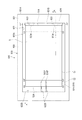
図1は、本発明の光学フィルターデバイスの第一実施形態である、光学フィルターデバイス600の概略構成を示す平面図である。図2は、図1のA−A線における断面図である。
光学フィルターデバイス600は、入射した検査対象光から、所定の目的波長の光を取り出して射出させる装置であり、筐体610と、筐体610の内部に収納される波長可変干渉フィルター5を備えている。このような光学フィルターデバイス600は、例えば測色センサー等の光学モジュールや、測色装置やガス分析装置等の電子機器に組み込むことができる。なお、光学フィルターデバイス600を備えた光学モジュールや電子機器の構成については、後に詳述する。
[First embodiment]
Hereinafter, a first embodiment according to the present invention will be described with reference to the drawings.
[Configuration of optical filter device]
FIG. 1 is a plan view showing a schematic configuration of an
The
[波長可変干渉フィルターの構成]
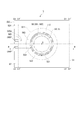
図3は、波長可変干渉フィルター5の概略構成を示す平面図である。図4は、図3のB−B線で切断した波長可変干渉フィルター5の概略構成を示す断面図である。
波長可変干渉フィルター5は、図3及び図4に示すように、本発明の第一基板に相当する固定基板51、及び本発明の第二基板に相当する可動基板52を備えている。これらの固定基板51及び可動基板52は、それぞれ例えば各種ガラスや、水晶等により形成されており、本実施形態では、石英ガラスにより構成されるものとする。そして、これらの基板51,52は、図4に示すように、接合膜53(第一接合膜531及び第二接合膜532)により接合されることで、一体的に構成されている。具体的には、固定基板51の第一接合部513、及び可動基板52の第二接合部523が、例えばシロキサンを主成分とするプラズマ重合膜等により構成された接合膜53により接合されている。
なお、以降の説明に当たり、固定基板51又は可動基板52の基板厚み方向から見た平面視、つまり、固定基板51、接合膜53、及び可動基板52の積層方向から波長可変干渉フィルター5を見た平面視を、フィルター平面視と称する。
[Configuration of wavelength tunable interference filter]
FIG. 3 is a plan view showing a schematic configuration of the variable
As shown in FIGS. 3 and 4, the variable
In the following description, the wavelength
固定基板51には、図4に示すように、本発明の一対の反射膜の一方を構成する固定反射膜54が設けられている。また、可動基板52には、本発明の一対の反射膜の他方を構成する可動反射膜55が設けられている。これらの固定反射膜54及び可動反射膜55は、反射膜間ギャップG1を介して対向配置されている。
そして、波長可変干渉フィルター5には、反射膜54,55間のギャップG1の距離(ギャップ寸法)を調整するのに用いられる、本発明のギャップ変更部に相当する静電アクチュエーター56が設けられている。この静電アクチュエーター56は、固定基板51に設けられた固定電極561と、可動基板52に設けられた可動電極562と、を備え、各電極561,562が対向することにより構成されている。これらの固定電極561,可動電極562は、電極間ギャップを介して対向する。ここで、これらの電極561,562は、それぞれ固定基板51及び可動基板52の基板表面に直接設けられる構成であってもよく、他の膜部材を介して設けられる構成であってもよい。
なお、本実施形態では、反射膜間ギャップG1が電極間ギャップよりも小さく形成される構成を例示するが、例えば波長可変干渉フィルター5により透過させる波長域によっては、反射膜間ギャップG1を電極間ギャップよりも大きく形成してもよい。
As shown in FIG. 4, the fixed
The wavelength
In the present embodiment, the configuration in which the gap G1 between the reflection films is formed smaller than the gap between the electrodes is exemplified. However, depending on the wavelength range transmitted by the wavelength
ここで、フィルター平面視において、可動基板52の一辺側(例えば、図3における辺C3−C4)は、固定基板51の辺C3´−C4´よりも外側に突出する。この可動基板52の突出部分は、固定基板51と接合されない電装部525であり、波長可変干渉フィルター5を固定基板51側から見た際に露出する面は、後述する電極パッド564P,565Pが設けられる電装面524となる。
Here, in the filter plan view, one side of the movable substrate 52 (for example, the side C <b> 3-C <b> 4 in FIG. 3) protrudes outside the side C <b> 3 ′ -C <b> 4 ′ of the fixed
(固定基板の構成)
固定基板51には、図4に示すように、エッチングにより電極配置溝511及び反射膜設置部512が形成されている。この固定基板51は、可動基板52に対して厚み寸法が大きく形成されており、固定電極561及び可動電極562間に電圧を印加した際の静電引力や、固定電極561の内部応力による固定基板51の撓みはない。
(Configuration of fixed substrate)
As shown in FIG. 4, the fixed
電極配置溝511は、フィルター平面視で、固定基板51のフィルター中心点Oを中心とした環状に形成されている(図3参照)。この電極配置溝511の溝底面は、固定電極561が配置される電極設置面511Aとなる。
反射膜設置部512は、前記平面視において、電極配置溝511の中心部から可動基板52側に突出して形成されている。この反射膜設置部512の突出先端面は、反射膜設置面512Aとなる。
The
The reflection
電極設置面511Aには、静電アクチュエーター56を構成する固定電極561が設けられている。この固定電極561は、電極設置面511Aのうち、後述する可動部521の可動電極562に対向する領域に設けられている。また、固定電極561上に、固定電極561及び可動電極562の間の絶縁性を確保するための絶縁膜が積層される構成としてもよい。
そして、固定基板51には、図3に示すように、固定電極561の外周縁に接続された固定引出電極563が設けられている。この固定引出電極563は、電極配置溝511から辺C3´−C4´側(電装部525側)に向かって形成された接続電極溝511B(図4参照)に沿って設けられている。この接続電極溝511Bには、可動基板52側に向かって突設されたバンプ565Aが設けられ、固定引出電極563は、バンプ565A上まで延出する。そして、バンプ565A上で可動基板52側に設けられた固定接続電極565に当接し、電気的に接続される。この固定接続電極565は、接続電極溝511Bに対向する領域から電装面524まで延出し、電装面524において固定電極パッド565Pを構成する。
A fixed
As shown in FIG. 3, the fixed
なお、本実施形態では、電極設置面511Aに1つの固定電極561が設けられる構成を示すが、例えば、フィルター中心点Oを中心とした同心円となる2つの電極が設けられる構成(二重電極構成)などとしてもよい。その他、固定反射膜54上に透明電極を設ける構成や、導電性の固定反射膜54を用い、当該固定反射膜54から固定側電装部に接続電極を形成してもよく、この場合、固定電極561として、接続電極の位置に応じて、一部が切り欠かれた構成などとしてもよい。
In the present embodiment, a configuration in which one fixed
反射膜設置部512は、上述したように、電極配置溝511と同軸上で、電極配置溝511よりも小さい径寸法となる略円柱状に形成され、当該反射膜設置部512の可動基板52に対向する反射膜設置面512Aを備えている。
この反射膜設置部512には、図4に示すように、固定反射膜54が設置されている。この固定反射膜54としては、例えばAg等の金属膜や、Ag合金等の合金膜を用いることができる。また、例えば高屈折層をTiO2、低屈折層をSiO2とした誘電体多層膜を用いてもよい。さらに、誘電体多層膜上に金属膜(又は合金膜)を積層した反射膜や、金属膜(又は合金膜)上に誘電体多層膜を積層した反射膜、単層の屈折層(TiO2やSiO2等)と金属膜(又は合金膜)とを積層した反射膜などを用いてもよい。
As described above, the reflective
As shown in FIG. 4, a fixed
また、固定基板51の光入射面(固定反射膜54が設けられない面)には、固定反射膜54に対応する位置に反射防止膜を形成してもよい。この反射防止膜は、低屈折率膜及び高屈折率膜を交互に積層することで形成することができ、固定基板51の表面での可視光の反射率を低下させ、透過率を増大させる。
Further, an antireflection film may be formed at a position corresponding to the fixed
そして、固定基板51の可動基板52に対向する面のうち、エッチングにより、電極配置溝511、反射膜設置部512、及び接続電極溝511Bが形成されない面は、第一接合部513を構成する。この第一接合部513には、第一接合膜531が設けられ、この第一接合膜531が、可動基板52に設けられた第二接合膜532に接合されることで、上述したように、固定基板51及び可動基板52が接合される。
Of the surfaces of the fixed
(可動基板の構成)
可動基板52は、フィルター中心点Oを中心とした円形状の可動部521と、可動部521と同軸であり可動部521を保持する保持部522と、を備えている。
(Configuration of movable substrate)
The
可動部521は、保持部522よりも厚み寸法が大きく形成される。この可動部521は、フィルター平面視において、少なくとも反射膜設置面512Aの外周縁の径寸法よりも大きい径寸法に形成されている。そして、この可動部521には、可動電極562及び可動反射膜55が設けられている。
なお、固定基板51と同様に、可動部521の固定基板51とは反対側の面には、反射防止膜が形成されていてもよい。このような反射防止膜は、低屈折率膜及び高屈折率膜を交互に積層することで形成することができ、可動基板52の表面での可視光の反射率を低下させ、透過率を増大させることができる。
The
Similar to the fixed
可動電極562は、所定の電極間ギャップを介して固定電極561に対向し、固定電極561と同一形状となる環状に形成されている。この可動電極562は、固定電極561とともに静電アクチュエーター56を構成する。また、可動基板52には、可動電極562の外周縁に接続された可動接続電極564が設けられている。この可動接続電極564は、可動部521から、固定基板51に設けられた接続電極溝511Bに対向する位置に沿って、電装面524に亘って設けられており、電装面524において、内側端子部に電気的に接続される可動電極パッド564Pを構成する。
また、可動基板52には、上述したように、固定接続電極565が設けられており、この固定接続電極565は、バンプ565A(図3参照)の形成位置で固定引出電極563に接続されている。
The
Further, as described above, the fixed
可動反射膜55は、可動部521の可動面521Aの中心部に、固定反射膜54とギャップG1を介して対向して設けられる。この可動反射膜55としては、上述した固定反射膜54と同一の構成の反射膜が用いられる。
なお、本実施形態では、上述したように、電極間ギャップが反射膜間ギャップG1の寸法よりも大きい例を示すがこれに限定されない。例えば、測定対象光として赤外線や遠赤外線を用いる場合等、測定対象光の波長域によっては、ギャップG1の寸法が、電極間ギャップの寸法よりも大きくなる構成としてもよい。
The movable
In the present embodiment, as described above, an example in which the interelectrode gap is larger than the dimension of the inter-reflection film gap G1 is shown, but the present invention is not limited to this. For example, when infrared rays or far infrared rays are used as the measurement target light, the gap G1 may be larger than the gap between the electrodes depending on the wavelength range of the measurement target light.
保持部522は、可動部521の周囲を囲うダイアフラムであり、可動部521よりも厚み寸法が小さく形成されている。このような保持部522は、可動部521よりも撓みやすく、僅かな静電引力により、可動部521を固定基板51側に変位させることが可能となる。この際、可動部521が保持部522よりも厚み寸法が大きく、剛性が大きくなるため、保持部522が静電引力により固定基板51側に引っ張られた場合でも、可動部521の形状変化が起こらない。したがって、可動部521に設けられた可動反射膜55の撓みも生じず、固定反射膜54及び可動反射膜55を常に平行状態に維持することが可能となる。
なお、本実施形態では、ダイアフラム状の保持部522を例示するが、これに限定されず、例えば、フィルター中心点Oを中心として、等角度間隔で配置された梁状の保持部が設けられる構成などとしてもよい。
The holding
In the present embodiment, the diaphragm-
可動基板52において、第一接合部513に対向する領域は、第二接合部523となる。この第二接合部523には、第二接合膜532が設けられ、上述したように、第二接合膜532が第一接合膜531に接合されることで、固定基板51及び可動基板52が接合される。
In the
[筐体の構成]
筐体610は、図2に示すように、本発明のベース部に相当するベース620と、リッド630と、を備え、内部に波長可変干渉フィルター5を収納する。
ベース620は、セラミック薄層を積層して焼成することで形成されたセラミック基板である。このベース620は、図1及び図2に示すように、リッド630に対向する面に、フィルター平面視において枠状となる側壁部621が設けられている。また、ベース620は、当該側壁部621に囲まれて形成された凹部622を有する。また、側壁部621のリッド630側の面であるリッド接合面621Aにリッド630が接合される。
[Case configuration]
As shown in FIG. 2, the
The
側壁部621の内側の側面のうち、固定基板51の辺C1´−C2´を含む側面51Aに対向する面621Bに、波長可変干渉フィルター5が固定部材624によって固定される(以下、固定面621Bと称する)。波長可変干渉フィルター5は、可動基板52を底部622A側に向け、図2に示すように、当該底部622Aと離間した状態で、固定基板51の側面51Aが固定面621Bに固定される。なお、波長可変干渉フィルター5をベース620に固定する固定構造については後に詳述する。
The wavelength
凹部622の底部622Aには、波長可変干渉フィルター5から出射された光(又は波長可変干渉フィルターに入射される光)を通過させるための光通過孔628が設けられている。光通過孔628には、例えば低融点ガラス等の接合剤により、例えばガラス板等の透光性部材629が接合されている。
A
また、凹部622の底部622Aには、筐体610外部に貫通する封止孔622Bが設けられている。この封止孔622Bは、光学フィルターデバイス600の製造時において、例えば筐体610内部の気体を吸引したり、不活性ガスに置換するための孔部であり、筐体610の内部を真空又は減圧した状態で、例えばAu等の封止部材622C(図2参照)により金属封止することができる。
In addition, a sealing
さらに、凹部622の底部622Aには、波長可変干渉フィルターの電極パッド564P,565Pに接続される内部端子622D(図1参照)が設けられている。この内部端子622Dの形成部分には、例えば筐体610の外部に貫通する貫通孔(図示略)が設けられ、当該貫通孔には内部端子622Dと電気的に接続される例えばAg等の金属部材が充填されている。この金属部材は、ベース620の外部に設けられた外部端子(図示略)に接続されており、これにより、内部端子622Dと外部端子とが電気接続されている。
Furthermore, an
リッド630は、フィルター平面視において、ベース620と同様の矩形状の外形を有し、光を透過可能なガラスによって形成されている。このリッド630は、ベース620に波長可変干渉フィルター5が配置された状態で、リッド接合面621Aに接合される。
The
[波長可変干渉フィルターの固定構造]
図1及び図2に示すように、波長可変干渉フィルター5の側面51Aが固定される固定面621Bには突出部623が設けられている。突出部623は、先端623Aで固定基板51の側面51Aに当接する。側面51Aと固定面621Bとは、突出部623によって規定された距離で離間し、側面51Aと固定面621Bとの間に設けられた固定部材624によって固定される。
[Fixed structure of tunable interference filter]
As shown in FIGS. 1 and 2, a
突出部623は、固定面621Bに直交する方向、当該固定面621Bから側壁部621に向かって突出している。この突出部623は、突出方向に向かうにしたがって、固定面621Bに平行な面方向の断面積が小さくなる形状、例えば、略半球状に形成されている。このような突出部623は、後述するが、熱硬化性樹脂や光硬化性樹脂等の液体から固体に硬化する材料を用いて形成される。
The protruding
このような突出部623は、図1に示すように、辺C1´−C2´に沿って互いに異なる位置に複数(図示例では2つ)設けられている。複数の突出部623は、それぞれ先端623Aで側面51Aに当接することにより、波長可変干渉フィルター5が固定面621Bに対して位置決めされる。
As shown in FIG. 1, a plurality of such projecting
ここで、突出部623は、固定部材624よりも弾性率が高い高弾性材料で形成されている。これにより、後述するように固定部材624の硬化収縮により、側面51Aから固定面621Bに向かう力が突出部623に作用しても、当該突出部623の変形を抑制できる。したがって、波長可変干渉フィルター5の固定面621Bに対する位置が変化することを抑制できる。
Here, the protruding
固定部材624は、固定面621Bに対して側面51Aを固定する。この固定部材624は、図1に示すように、固定基板51の辺C1´−C2´に沿って側面51Aの全面に設けられている。図2に示すように、波長可変干渉フィルター5は、可動基板52を底部622A側に向けた状態で、固定部材624によって固定面621Bに固定されている。本実施形態では、波長可変干渉フィルター5の側面51A以外の面と、ベース620との間に間隙が設けられている。例えば、図2に示すように、可動基板52の底部622Aに対向する下面52Bと、当該底部622Aとの間には、間隙CL1が設けられている。なお、固定基板51とリッド630との間にも間隙が設けられている。
The fixing
ここで、波長可変干渉フィルター5に、外乱等により基板厚み方向の力が作用すると、固定部材624によって固定された当該辺C1´−C2´を含む側面51Aを固定端とする、基板厚み方向(図2の矢印M)に沿った振動(以下、フィルター振動とも称する)が生じる場合がある。このフィルター振動のうち、波長可変干渉フィルター5の一次共振による振動(一次共振振動)では、フィルター平面視において、固定端側の側面51Aから最も離れた可動基板52の側面52A側の端部(自由端)において、振幅が最大となる。なお、フィルター振動は、外乱以外に、静電アクチュエーター56の駆動によって可動部521が移動した際の反動によっても誘起される場合がある。
Here, when a force in the substrate thickness direction is applied to the wavelength
本実施形態では、基板厚み方向(図2の矢印M方向)における、下面52Bと底部622Aとの間の間隙CL1の寸法h1(波長可変干渉フィルター5の静止時)は、フィルター振動が発生したとしても、自由端である側面52Aの下端(側面52Aと下面52Bとの交差部分)における最大振幅(一次共振振動における振幅)よりも大きくなるように設定されている。例えば、固定基板51の寸法が約10mmで、かつ上記最大振幅が数μmの場合、間隙CL1の寸法h1は数十μm以上(例えば20μm以上)に設定されている。これにより、フィルター振動が発生した場合でも、可動基板52が底部622Aに接触することを抑制できる。
なお、フィルター振動が発生した際の、上記側面52A側の下面52Bの最大振幅は、波長可変干渉フィルター5の寸法、各基板51,52、固定部材624の弾性率、及び外乱振動の大きさ等に応じて変化するものであり、シミュレーションや実験等で取得すればよい。
In the present embodiment, the dimension h1 of the gap CL1 between the
Note that the maximum amplitude of the
また、本実施形態では、固定部材624は、このフィルター振動によって、側面51A側を固定端として回転しようとする波長可変干渉フィルター5からの応力を受けて弾性変形可能な弾性率(例えば、500MPa以下)を有する。このように、固定部材624が弾性変形することにより、フィルター振動を吸収することができ、当該フィルター振動の影響によりギャップG1の寸法が変動して波長可変干渉フィルター5の分解能が低下することを抑制できる。
In the present embodiment, the fixing
ここで、固定部材624は、弾性率が小さいほど、固定力が小さくなる。すなわち、固定部材624の弾性率を小さくすることで、弾性変形によりフィルター振動を抑制できるものの、固定力が低下して波長可変干渉フィルター5の脱落のおそれがある。このため、弾性率の下限値は、波長可変干渉フィルター5の質量や寸法等に応じて波長可変干渉フィルター5が脱落を抑制可能な固定力を得るのに十分な値に設定する。一方で、弾性率の上限値は、同様に、フィルター振動に応じた弾性変形を許容する値に設定する。
このような固定部材624として、例えばシリコーン系接着剤を用いることができる。また、固定部材624の弾性率としては、例えば、10MPa以上500MPa以下であることが好ましく、50MPa以上100MPa以下であることがより好ましい。これにより、波長可変干渉フィルター5の脱落を抑制しつつ、フィルター振動を効果的に抑制できる。
Here, the fixing
As such a fixing
[光学フィルターデバイスの製造方法]
次に、上述したような光学フィルターデバイス600の製造方法について図面に基づいて説明する。
図5は、光学フィルターデバイス600の製造工程の一例を示す工程図である。
また、図6〜図10は、図5に示すデバイス組立工程における、波長可変干渉フィルター5やベース620等の部材を模式的に示している。なお、図6(A)は、ベース620を底部622Aに向かってみた場合の上面図であり、図6(B)は、図6(A)のC−C線で切断した切断面を示す断面図であり、図7〜図9についても同様である。
ここで、以下の説明では、底部622Aに直交する方向をZ方向、Z方向に直交し、かつ、固定面621Bに直交する方向をX方向、X方向及びZ方向に直交する方向をY方向とする。また、底部622Aを基点としてベース620から離れる方向を+Z方向とする。
また、図6〜図9では、Z方向を鉛直方向に平行、かつ、下から上に向かう方向に一致させてベース620が配置されている状態を示す。一方、図10では、Z方向を鉛直方向に一致させてベース620が配置されている状態を示す。
[Method of manufacturing optical filter device]
Next, a method for manufacturing the
FIG. 5 is a process diagram showing an example of a manufacturing process of the
6 to 10 schematically show members such as the variable
Here, in the following description, the direction orthogonal to the bottom 622A is the Z direction, the direction orthogonal to the Z direction and the direction orthogonal to the fixed
6 to 9 show a state in which the
図5に示す、光学フィルターデバイス600の製造工程では、光学フィルターデバイス600を構成する波長可変干渉フィルター5を製造するフィルター準備工程(S1)、ベース620を準備するベース準備工程(S2)、リッド630を準備するリッド準備工程(S3)をそれぞれ実施した後、これら波長可変干渉フィルター5、ベース620、及びリッド630を用いて光学フィルターデバイス600を組み立てるデバイス組み立て工程(S4)を実施する。
In the manufacturing process of the
(フィルター準備工程)
フィルター準備工程S1では、まず、固定基板51及び可動基板52を適宜エッチング処理等により形成する。そして、固定基板51に対しては、固定電極561及び固定引出電極563を成膜し、その後、固定反射膜54を成膜する。また、可動基板52に対しては、可動電極562、可動接続電極564、固定接続電極565、及び各電極パッド564P,565Pを成膜した後、可動反射膜55を成膜する。この後、固定基板51及び可動基板52を、接合膜53を介して接合することで波長可変干渉フィルター5が得られる。
(Filter preparation process)
In the filter preparation step S1, first, the fixed
(ベース基板準備工程)
ベース準備工程S2では、まず、ベース620の外形を形成する。具体的には、まず、セラミック基板の形成素材であるシートを積層した焼成前基板に、切削加工やレーザー加工等を適宜施し、凹部622や光通過孔628を有するベース620の形状を成形する。そして、焼成前基板を焼成することで、ベース620を形成する。
この後、図示を省略するが、内部端子622Dと、外部端子(図示略)とを電気的に接続するための貫通孔(図示略)を底部622Aに形成し、形成した貫通孔には導電性部材を充填する。そして、内部端子622D及び外部端子を形成する。
(Base substrate preparation process)
In the base preparation step S2, first, the outer shape of the
Thereafter, although not shown, a through hole (not shown) for electrically connecting the
(リッド準備工程)
リッド準備工程S3では、所定の厚みのガラスの板材を、ベース620と同様の矩形状の部分に分割し、複数のリッド630を同時に形成する。
(Lid preparation process)
In the lid preparation step S3, a glass plate material having a predetermined thickness is divided into rectangular portions similar to the
(デバイス組み立て工程)
デバイス組み立て工程S4では、波長可変干渉フィルター5をベース620に固定した後、リッド630をベース620に接合して光学フィルターデバイス600を形成する。
(Device assembly process)
In the device assembly step S4, after the wavelength
このデバイス組み立て工程S4では、まず、ベース620の凹部622の固定面621Bに突出部623を形成する突出部形成工程を実施する(S41)。
本実施形態では、図6に示すように、固定面621Bの波長可変干渉フィルター5の固定位置に、熱硬化性樹脂や光硬化性樹脂等の液状の硬化材料を塗布し、硬化させることで固定面621Bを形成する。すなわち、液状の硬化材料は、固定面621Bに塗布されると、表面張力により略半球状となる。この略半球状の硬化材料を硬化させる。このようにして形成された突出部623は、固定面621Bから離れるにしたがって固定面621Bに平行な切断面の面積が小さくなる、略半球状に形成される。なお、突出部623の形状やサイズは、硬化材料の粘度や、塗布量によって調整することができる。
In the device assembly step S4, first, a protruding portion forming step for forming the protruding
In the present embodiment, as shown in FIG. 6, a liquid curable material such as a thermosetting resin or a photocurable resin is applied to the fixing position of the wavelength
次に、固定面621Bの波長可変干渉フィルター5の固定位置に固定部材624を塗布する、固定部材塗布工程を実施する(S42)。
固定部材624は、図7に示すように、固定面621Bに直交する方向における寸法が、突出部623の寸法以上となる塗布量で、固定面621Bに塗布される。これにより、波長可変干渉フィルター5の側面51Aを、突出部623の先端623Aに接触する前に、固定部材624に接触させることができ、側面51Aが固定部材624に接触しないことによる接合不良を抑制できる。
Next, a fixing member application step of applying the fixing
As shown in FIG. 7, the fixing
次に、波長可変干渉フィルター5を固定位置に固定するフィルター固定工程を実施する(S43)。
フィルター固定工程S43では、波長可変干渉フィルター5を、固定部材624に接触しないように底部622Aに配置した後(図7参照)、底部622Aと波長可変干渉フィルター5とを離間させた状態で、波長可変干渉フィルター5の側面51Aを突出部623の先端623Aに当接させ、波長可変干渉フィルター5をベース620に固定する。
Next, a filter fixing step of fixing the wavelength
In the filter fixing step S43, the wavelength
具体的には、図8に示すように、波長可変干渉フィルター5の辺C1−C4を含む端面5Aと、当該端面5Aに対向する側壁部621の内面621Cとの間の空間CL2(図7参照)にガイド部材71を配置する。同様に、波長可変干渉フィルター5の辺C2−C3を含む端面5Bと、当該端面5Bに対向するベース620の内面621Dとの間の空間CL3(図7参照)にガイド部材71を配置する。また、波長可変干渉フィルター5の底部622Aとは反対側の面、すなわち固定基板51の上面51B上に位置決め部材72を配置する。
Specifically, as shown in FIG. 8, a space CL2 between the
ガイド部材71は、波長可変干渉フィルター5の移動方向を規制し、固定面621Bに直交するX方向に移動させる。ガイド部材71は、端面5Bに直交するY方向における空間CL2の寸法と、厚み寸法が略同一の板状部材であり、ガラス等で形成される。ガイド部材71が空間CL2に挿入された状態で、波長可変干渉フィルター5が、ガイド部材71の表面に沿って、X方向に移動される。
The
位置決め部材72は、後述するように、波長可変干渉フィルター5のZ方向の位置決めを行い、間隙CL1の寸法h1(図2参照)を所望値に設定するための部材である。この位置決め部材72は、平板状であり、ガラス等で形成される。位置決め部材72は、波長可変干渉フィルター5に当接するフィルター当接面72Aと、当該フィルター当接面72Aとは反対側の上面72Bとを有する。位置決め部材72が波長可変干渉フィルター5の上に配置された状態で、フィルター当接面72A及び上面72BはZ方向に直交する。
ここで、Z方向における、位置決め部材72の厚み寸法h2は、凹部622の深さ寸法H、及び波長可変干渉フィルター5の厚み寸法h3に対して、間隙CL1の寸法h1が、上述の所望値となるように設定されている。すなわち、各寸法h1,h2,h3の和が、凹部622の深さ寸法Hとなるように、位置決め部材72の厚み寸法h2が設定されている。
As will be described later, the positioning
Here, the thickness dimension h2 of the positioning
図8に示すように、ガイド部材71及び位置決め部材72を配置した状態で、波長可変干渉フィルター5をX方向に突出部623に向かって移動させる。波長可変干渉フィルター5は、X方向に移動され、図9に示すように、側面51Aが突出部623の先端623Aに当接される。この際、側面51Aの全面に固定部材624が密着している。
ここで、波長可変干渉フィルター5のY方向に交差する一対の端面5A,5Bのそれぞれに当接するようにガイド部材71が配置されている。これにより、波長可変干渉フィルター5をX方向に移動させる際に、Y方向における位置が変化することを抑制できる。
As shown in FIG. 8, the wavelength
Here, the
次に、図10に示すように、リッド接合面621Aに当接する第一挟持部材73と、Z方向において当該第一挟持部材73とは逆側からベース620に当接する第二挟持部材74とで、Z方向の両側からベース620を挟持し、+Z方向が鉛直方向の上から下に向かう方向となるように上下を反転させて、波長可変干渉フィルター5のZ方向の位置決めを行う。
すなわち、ベース620の上下を反転させると、波長可変干渉フィルター5及び位置決め部材72が+Z方向(下方)に移動する。そして、第一挟持部材73のリッド接合面621Aに当接する当接平面73A(Z方向に直交する面)に、位置決め部材72の上面72Bが当接し、Z方向において波長可変干渉フィルター5が位置決めされる。
上述のように、凹部622の深さ寸法H、間隙CL1の寸法h1、位置決め部材72の厚み寸法h2、及び波長可変干渉フィルター5の厚み寸法h3は、寸法h1が所望値となるように設定されているので、可動基板52の下面52Bと底部622Aとの間に所望の寸法h1の間隙CL1が設けられる。
Next, as shown in FIG. 10, a
That is, when the upper and lower sides of the base 620 are inverted, the wavelength
As described above, the depth dimension H of the
そして、波長可変干渉フィルター5が、位置決めされた状態で固定部材624を硬化させて、波長可変干渉フィルター5の側面51Aと、ベース620の固定面621Bとを固定部材624で固定する。固定部材624を硬化させた後、ガイド部材71及び位置決め部材72を取り除く。このようにして、波長可変干渉フィルター5が、側面51Aの略全面の一箇所で、ベース620に対して固定される。そして、側面51A以外では、波長可変干渉フィルター5の表面と、ベース620との間に間隙が設けられている(図1及び図2参照)。すなわち、固定基板51及び可動基板52の表面のうちの外部に露出している領域と、ベース620とが、間隙を介して配置されている。
Then, the
なお、固定基板51の上面51Bとリッド630との距離は寸法h2以上となる(厳密には、寸法h2と接合部材の厚み寸法との和)。したがって、上面51Bとリッド630との距離の最小値を、寸法h2によって規定することができる。例えば、寸法h1と同様に、固定基板51の固定端となる側面51Aとは反対側の自由端側の上端の最大振幅よりも大きくなるように、寸法h2を設定することにより、上面51Bがリッド630に接触することを抑制できる。
The distance between the
次に、配線接続工程を実施する(S44)。このS44では、ワイヤーボンディングにより、波長可変干渉フィルター5の各電極パッド564P,565Pと、各内部端子622Dとをそれぞれワイヤーで接続する。
この後、ベース620及びリッド630を接合するリッド接合工程を実施する(S45)。なお、リッド630の接合とともに、光通過孔628を覆う位置に透光性部材629を接合する。このS45では、例えば真空チャンバー装置等において、真空雰囲気に設定された環境下でベース620と、透光性部材629及びリッド630とを接合する。
以上により、光学フィルターデバイス600が製造される。
Next, a wiring connection process is performed (S44). In S44, the
Thereafter, a lid joining step for joining the
Thus, the
[実施形態の作用効果]
本実施形態では、波長可変干渉フィルター5の固定基板51の一箇所を、固定部材624でベース620に固定する。そして、波長可変干渉フィルター5の固定部材624による固定部分以外の部分と、ベース620とが間隙(間隙CL1)を介して配置されている。
ここで、固定基板51を一箇所で固定した場合、例えば、外乱の影響により、上述のようにフィルター振動が生じる場合がある。
本実施形態では、波長可変干渉フィルター5が側面51Aの一箇所で固定部材624により固定されているものの、固定部材624の固定部分以外の部分では、ベース620との間に間隙CL1が設けられており、ベース620に接触していない。このため、外乱による振動がベース620から各基板51,52に伝達することを抑制でき、外乱の影響による上記フィルター振動の発生を抑制できる。したがって、上記フィルター振動による基板の各基板51,52の歪みを抑制でき、波長可変干渉フィルター5の分解能の低下を抑制できる。
[Effects of Embodiment]
In the present embodiment, one portion of the fixed
Here, when the fixed
In the present embodiment, the wavelength
本実施形態では、固定部材は、基板の厚み方向に沿った側面を一箇所で固定している。
通常、固定基板51の厚み方向に対する剛性(撓みに対する耐性)は、平面方向に対する剛性よりも低い。このため、上述のように、側面51Aの一箇所に固定部材624を設けることで、固定部材624からの応力の方向を側面51Aに沿った平面方向とすることができ、固定部材624からの応力による固定基板51の歪みを抑制でき、波長可変干渉フィルター5の分解能の低下を抑制できる。
In the present embodiment, the fixing member fixes the side surface along the thickness direction of the substrate at one location.
Usually, the rigidity (resistance to bending) of the fixed
本実施形態では、側面51Aの厚み方向に交差する辺C1´−C2´に沿って固定部材624が設けられている。このような構成では、例えば、側面51Aの略全面に固定部材624を設けることができ、固定部材624の側面51Aの一部を固定する場合と比べて、固定面積を大きくすることができる。これにより、固定部材624の弾性率を低くしたとしても、固定部材624による固定力を所望値以上とすることができ、固定基板51の脱落を抑制できる。
In the present embodiment, the fixing
本実施形態では、固定部材624は、側面51Aを固定端とする基板の回転に応じた応力で弾性変形する。
ここで、固定基板51の側面51Aを一箇所で固定する構成では、上述のように、外乱の影響でフィルター振動が発生する場合がある。この場合、固定位置を固定端(基点)として回転しようとする応力が、固定部材624や固定基板51に作用する。
これに対して、本実施形態では、固定部材624が、上記応力を受けて弾性変形する程度の低弾性材料で形成されている。このため、フィルター振動を誘起する力が、光学フィルターデバイス600や、波長可変干渉フィルター5に作用した場合でも、固定部材624が弾性変形することで上記フィルター振動が残留することを抑制できる。
In the present embodiment, the fixing
Here, in the configuration in which the
On the other hand, in this embodiment, the fixing
また、本実施形態では、ギャップ変更部としての静電アクチュエーター56によって可動部521が駆動される。上述のように、この可動部521の駆動に応じて、波長可変干渉フィルター5に上記フィルター振動が誘起される場合がある。
これに対して、本実施形態では、上記フィルター振動が生じた場合でも、固定部材624が弾性変形することにより、上記フィルター振動の残留を好適に抑制できる。また、間隙CL1を設けることにより、波長可変干渉フィルター5とベース620との接触を抑制でき、接触の衝撃による波長可変干渉フィルター5の劣化や、脱落を抑制できる。
In the present embodiment, the
On the other hand, in this embodiment, even when the filter vibration is generated, the fixing
本実施形態では、突出部623が、ベース620の固定面621Bから側面51Aに向かって突出し、当該側面51Aに当接している。
このような構成では、側面51Aと固定面621Bとの間の距離を、突出部623の突出方向の寸法で規定することができ、側面51Aと固定面621Bを離間させつつも、ベース620に対して固定基板51を位置決めして固定することができる。
In the present embodiment, the protruding
In such a configuration, the distance between the
本実施形態では、突出部623は、複数設けられ、突出方向に向かうにしたがって、固定面621Bに沿った方向の断面積が小さくなる曲面形状を有する。
このような構成では、側面51Aと突出部623との間の接触面積を小さくできるため、外乱による振動がベース620から固定基板51に伝達されることをより確実に抑制できる。また、複数の突出部623で当接することで、接触面積を小さくしながらも位置決め精度を向上させることができる。
In the present embodiment, a plurality of projecting
In such a configuration, the contact area between the
本実施形態では、突出部623は、ベース620の固定面621Bに設けられ、固定部材624よりも高い弾性率を有する材料で形成されている。
このような構成では、例えば、熱硬化性樹脂や光硬化性樹脂等の液体から固体に硬化する材料を、固定面621Bに塗布し硬化させることで、突出部623を容易に形成することができる。また、突出部623の形成材料が硬化収縮した際の応力が、波長可変干渉フィルター5に作用することがないため、当該硬化収縮による歪みがなく、突出部623を設けることによる波長可変干渉フィルター5の分解能の低下を抑制できる。また、高弾性の材料(例えば、エポキシ樹脂等)を用いて突出部623を形成したとしても、硬化収縮による波長可変干渉フィルター5の歪みを抑制できる。
In the present embodiment, the
In such a configuration, for example, the
ここで、本実施形態では、固定部材624として、シリコーン系接着剤等の低弾性材料を用いて、波長可変干渉フィルター5をベース620に固定している。これにより、波長可変干渉フィルター5の各基板51,52とベース620との間での熱膨張係数差により、膨張量(又は収縮量)に差が生じたとしても、固定部材624を変形させることができ、上記熱膨張係数差によって固定基板51に作用する応力で、当該固定基板51が撓むことを抑制できる。
Here, in this embodiment, the wavelength
また、固定部材624として、突出部623よりも弾性率が低い低弾性材料を用いている。例えば、固定部材624としてシリコーン系接着剤を用いる場合、突出部623としてのエポキシ樹脂を使用できる。これにより、固定部材624が硬化収縮することで、波長可変干渉フィルター5に+X方向の応力が作用し、突出部623がX方向に押圧されても、突出部623の変形を抑制でき、波長可変干渉フィルター5の位置ズレを抑制できる。
また、波長可変干渉フィルター5のX方向の位置が突出部623で規制された状態で、固定部材624に硬化収縮が発生したとして、固定部材624として低弾性材料を用いることにより、固定部材624を弾性変形させることができ、波長可変干渉フィルター5の脱落を抑制できる。
Further, as the fixing
Further, assuming that the fixing
[第二実施形態]
次に、本発明に係る第二実施形態について、図面に基づいて説明する。
第二実施形態では、上記第一実施形態の光学フィルターデバイス600が組み込まれた光学モジュールである測色センサー3、及び光学フィルターデバイス600が組み込まれた電子機器である測色装置1を説明する。
[Second Embodiment]
Next, 2nd embodiment which concerns on this invention is described based on drawing.
In the second embodiment, a
[測色装置の概略構成]
図11は、測色装置1の概略構成を示すブロック図である。
測色装置1は、本発明の電子機器である。この測色装置1は、図11に示すように、検査対象Xに光を射出する光源装置2と、測色センサー3と、測色装置1の全体動作を制御する制御装置4と、を備える。そして、この測色装置1は、光源装置2から射出され検査対象Xにて反射された検査対象光を測色センサー3にて受光する。そして、測色装置1は、受光した測色センサー3から出力される検出信号に基づいて、検査対象光の色度、すなわち検査対象Xの色を分析して測定する装置である。
[Schematic configuration of color measuring device]
FIG. 11 is a block diagram illustrating a schematic configuration of the
The
[光源装置の構成]
光源装置2は、光源21、複数のレンズ22(図11には1つのみ記載)を備え、検査対象Xに対して白色光を射出する。また、複数のレンズ22には、コリメーターレンズが含まれてもよく、この場合、光源装置2は、光源21から射出された白色光をコリメーターレンズにより平行光とし、図示しない投射レンズから検査対象Xに向かって射出する。なお、本実施形態では、光源装置2を備える測色装置1を例示するが、例えば検査対象Xが液晶パネル等の発光部材である場合、光源装置2が設けられない構成としてもよい。
[Configuration of light source device]
The
[測色センサーの構成]
測色センサー3は、本発明の光学モジュールを構成し、上記第一実施形態の光学フィルターデバイス600を備えている。この測色センサー3は、図11に示すように、光学フィルターデバイス600と、光学フィルターデバイス600を透過した光を受光する検出部31と、波長可変干渉フィルター5の透過光の波長を変更する電圧制御部32と、を備える。
また、測色センサー3は、波長可変干渉フィルター5に対向する位置に、検査対象Xで反射された反射光(検査対象光)を、内部に導光する図示しない入射光学レンズを備えている。そして、この測色センサー3は、光学フィルターデバイス600内の波長可変干渉フィルター5により、入射光学レンズから入射した検査対象光のうち、所定波長の光を分光し、分光した光を検出部31にて受光する。
[Configuration of colorimetric sensor]
The
Further, the
検出部31は、複数の光電交換素子により構成されており、受光量に応じた電気信号を生成する。ここで、検出部31は、例えば回路基板311を介して、制御装置4に接続されており、生成した電気信号を受光信号として制御装置4に出力する。
また、この回路基板311には、筐体610の外側表面に形成された外側端子が接続されており、回路基板311に形成された回路を介して、電圧制御部32に接続されている。
このような構成では、回路基板311を介して、光学フィルターデバイス600及び検出部31を一体的に構成でき、測色センサー3の構成を簡略化することができる。
The
The
In such a configuration, the
電圧制御部32は、回路基板311を介して光学フィルターデバイス600の外側端子に接続される。そして、電圧制御部32は、制御装置4から入力される制御信号に基づいて、電極パッド564P,565Pに所定のステップ電圧を印加することで、静電アクチュエーター56を駆動させる。これにより、電極間ギャップに静電引力が発生し、保持部522が撓むことで、可動部521が固定基板51側に変位し、反射膜間ギャップG1を所望の寸法に設定することが可能となる。
The
[制御装置の構成]
制御装置4は、本発明の処理部に相当し、測色装置1の全体動作を制御する。
この制御装置4としては、例えば汎用パーソナルコンピューターや、携帯情報端末、その他、測色専用コンピューター等を用いることができる。
そして、制御装置4は、図11に示すように、光源制御部41、測色センサー制御部42、及び測色処理部43等を備えて構成されている。
光源制御部41は、光源装置2に接続されている。そして、光源制御部41は、例えば利用者の設定入力に基づいて、光源装置2に所定の制御信号を出力し、光源装置2から所定の明るさの白色光を射出させる。
測色センサー制御部42は、測色センサー3に接続されている。そして、測色センサー制御部42は、例えば利用者の設定入力に基づいて、測色センサー3にて受光させる光の波長を設定し、この波長の光の受光量を検出する旨の制御信号を測色センサー3に出力する。これにより、測色センサー3の電圧制御部32は、制御信号に基づいて、利用者が所望する光の波長のみを透過させるよう、静電アクチュエーター56への印加電圧を設定する。
測色処理部43は、検出部31により検出された受光量から、検査対象Xの色度を分析する。
[Configuration of control device]
The control device 4 corresponds to the processing unit of the present invention, and controls the overall operation of the
As this control device 4, for example, a general-purpose personal computer, a portable information terminal, a color measurement dedicated computer, or the like can be used.
As shown in FIG. 11, the control device 4 includes a light
The light
The colorimetric
The
[第二実施形態の作用効果]
本実施形態の測色装置1は、上記第一実施形態のような光学フィルターデバイス600を備えている。上述したように、光学フィルターデバイス600は、接合時における可動基板52の撓みや反りを低減でき、波長可変干渉フィルター5から所望波長の光を精度よく出射させることができる。
したがって、光学モジュールである測色センサー3は、検出部31により所望波長の光量を高精度に検出することが可能となる。これにより、電子機器である測色装置1は、光学フィルターデバイス600の波長可変干渉フィルター5を制御することで、検査対象Xに対する高精度な測色処理を実施できる。
[Operational effects of the second embodiment]
The
Therefore, the
[実施形態の変形]
なお、本発明は上述の実施形態に限定されるものではなく、本発明の目的を達成できる範囲での変形、改良等は本発明に含まれるものである。
上記各実施形態では、波長可変干渉フィルター5の固定基板51の側面51Aの全面を固定する構成を例示したが、本発明はこれに限定されない。例えば、固定基板51の側面51Aの一部を一箇所で固定する構成でもよい。この場合、固定面積を小さくすることができ、固定部材624からの応力による固定基板51の歪みをより確実に抑制できる。
また、側面51Aに限らず、固定基板51の辺C1´−C4´を含む側面や、辺C2´−C3´を含む側面の一箇所を固定してもよい。また、側面に限らず、底部622Aに対向する可動基板の下面52Bの一部を一箇所で固定してもよい。
また、固定基板51の4つの頂点C1〜C4のうちの1つを含む角部を1箇所で固定してもよく、同様に、可動基板52の4つの頂点C1´〜C4´のうちの1つを含む角部を1箇所で固定してもよい。
上述のいずれの場合も、突出部623は、波長可変干渉フィルター5における固定部材624の固定位置と、当該固定位置に対向する凹部622の内面との間に設けられる。
例えば、頂点C1´を含む角部、すなわち頂点C1´を跨ぎ、辺C1´−C2´を含む側面51Aから、辺C1´−C4´を含む側面を固定する場合、凹部622の内面における、固定部材624に固定される各側面の固定位置と対向する位置に、突出部623が設けられる。
[Modification of Embodiment]
In addition, this invention is not limited to the above-mentioned embodiment, The deformation | transformation in the range which can achieve the objective of this invention, improvement, etc. are included in this invention.
In each of the above embodiments, the configuration in which the
Further, not only the
Further, the corner including one of the four vertices C1 to C4 of the fixed
In any of the cases described above, the
For example, when the side surface including the side C1′-C4 ′ is fixed from the
上記各実施形態では、波長可変干渉フィルター5の固定基板51を固定する構成を例示したが、本発明はこれに限定されず、可動基板52をベース620に固定する構成としてもよい。例えば、固定基板51をベース620側に向けて波長可変干渉フィルター5を配置し、可動基板52をベース620に固定する構成が挙げられる。
なお、固定基板51及び可動基板52の両方を固定部材624で固定してもよい。例えば、固定基板51の辺C1´−C4´側の波長可変干渉フィルター5の側面や、辺C2´−C3´側の波長可変干渉フィルター5の側面を固定部材624で固定する際に、可動基板52の側面も共に固定してもよい。
In each of the above embodiments, the configuration in which the fixed
Note that both the fixed
上記各実施形態では、突出部623は、ベース620に設けられている構成を例示したが、本発明はこれに限定されない。例えば、固定基板51及び可動基板52の少なくとも一方、すなわち波長可変干渉フィルター5側に突出部623が形成されてもよく、波長可変干渉フィルター5とベース620との両側に突出部623が形成されてもよい。
In each said embodiment, although the
上記各実施形態では、突出部623が、突出方向に向かうにしたがって固定面621Bに平行な面方向の断面積が小さくなる半球状である構成を例示したが、本発明はこれに限定されず、例えば、錘状や台形状であってもよい。
また、突出部623は、突出方向に向かうにしたがって上述のように断面積が小さくなる形状に限定されず、断面積が略変化しない柱状の形状でもよい。なお、断面積が小さくなるように例えば半球状とすることにより、突出部623の剛性を確保しつつ、波長可変干渉フィルター5とベース620との間の接触面積を小さくすることができる。
In each of the above-described embodiments, the protruding
Further, the protruding
上記各実施形態では、ギャップ変更部として、固定電極561、及び可動電極562に電圧を印加することで、静電引力により反射膜間ギャップG1の大きさを変更する静電アクチュエーター56を備える構成を例示したが、これに限定されない。
例えば、ギャップ変更部として、誘導アクチュエーターを用いてもよい。この場合、固定電極561の代わりに、第一誘導コイルを配置し、可動電極562の代わりに第二誘導コイル又は永久磁石を配置する構成を例示できる。
さらに、ギャップ変更部として、圧電アクチュエーターを用いてもよい。この場合、保持部522に下部電極層、圧電膜、及び上部電極層を積層配置させ、下部電極層及び上部電極層の間に印加する電圧を入力値として可変させることで、圧電膜を伸縮させて保持部522を撓ませる構成を例示できる。
また、上記各実施形態では、ギャップ変更部としての静電アクチュエーター56を一対の基板の一方のみに設けた構成を例示したが、本発明はこれに限定されず、ギャップ変更部を両方の基板に設けてもよい。
In each of the above-described embodiments, the gap change unit includes the
For example, an induction actuator may be used as the gap changing unit. In this case, a configuration in which the first induction coil is arranged instead of the fixed
Furthermore, a piezoelectric actuator may be used as the gap changing unit. In this case, the lower electrode layer, the piezoelectric film, and the upper electrode layer are stacked on the holding
Moreover, in each said embodiment, although the structure which provided the
上記各実施形態では、反射膜間ギャップG1を変更可能に構成された波長可変干渉フィルター5を例示したが、これに限定されず、反射膜間ギャップG1の大きさが固定された干渉フィルターであってもよい。
また、上記各実施形態では、波長可変干渉フィルター5として、一対の基板51,52と、各基板51,52のそれぞれに設けられた一対の反射膜54,55を備える構成を例示したが、これに限定されない。例えば、可動基板52が設けられない構成とし、固定基板51を筐体610に固定する構成としてもよい。この場合、例えば、基板(固定基板)の一面に第一反射膜、ギャップスペーサ、及び第二反射膜を積層形成し、第一反射膜と第二反射膜とがギャップを介して対向する構成とする。当該構成では、一枚の基板からなる構成となり、分光素子をより薄型化することができる。
In each of the above embodiments, the wavelength
In each of the above-described embodiments, the wavelength
また、本発明の電子機器として、第二実施形態において測色装置1を例示したが、その他、様々な分野により本発明の光学フィルターデバイス、光学モジュール、電子機器を用いることができる。
以下、本発明の光学フィルターデバイスを利用した電子機器の変形例について説明する。なお、以下に例示する電子機器は、上記光学フィルターデバイス600を備え、波長可変干渉フィルター5が筐体610に収納されている。
Moreover, although the
Hereinafter, modified examples of the electronic apparatus using the optical filter device of the present invention will be described. Note that an electronic apparatus exemplified below includes the
本発明の電子機器は、例えば、特定物質の存在を検出するための光ベースのシステムとして用いることができる。このようなシステムとしては、例えば、本発明の光学フィルターデバイスが備える波長可変干渉フィルターを用いた分光計測方式を採用して特定ガスを高感度検出する車載用ガス漏れ検出器や、呼気検査用の光音響希ガス検出器等のガス検出装置を例示できる。
このようなガス検出装置の一例を以下に図面に基づいて説明する。
The electronic device of the present invention can be used, for example, as a light-based system for detecting the presence of a specific substance. As such a system, for example, an in-vehicle gas leak detector that detects a specific gas with high sensitivity by adopting a spectroscopic measurement method using a variable wavelength interference filter provided in the optical filter device of the present invention, or a breath test A gas detection device such as a photoacoustic rare gas detector can be exemplified.
An example of such a gas detection device will be described below with reference to the drawings.
図12は、波長可変干渉フィルターを備えたガス検出装置の一例を示す概略図である。
図13は、図12のガス検出装置の制御系の構成を示すブロック図である。
このガス検出装置100は、図12に示すように、センサーチップ110と、吸引口120A、吸引流路120B、排出流路120C、及び排出口120Dを備えた流路120と、本体部130と、を備えて構成されている。
本体部130は、流路120を着脱可能な開口を有するセンサー部カバー131、排出手段133、筐体134、光学部135、フィルター136、光学フィルターデバイス600、及び受光素子137(検出部)等を含む検出装置と、検出された信号を処理し、検出部を制御する制御部138、電力を供給する電力供給部139等から構成されている。また、光学部135は、光を射出する光源135Aと、光源135Aから入射された光をセンサーチップ110側に反射し、センサーチップ側から入射された光を受光素子137側に透過するビームスプリッター135Bと、レンズ135C,レンズ135D,レンズ135Eと、により構成されている。
また、図13に示すように、ガス検出装置100の表面には、操作パネル140、表示部141、外部とのインターフェイスのための接続部142、電力供給部139が設けられている。電力供給部139が二次電池の場合には、充電のための接続部143を備えてもよい。
さらに、ガス検出装置100の制御部138は、図13に示すように、CPU等により構成された信号処理部144、光源135Aを制御するための光源ドライバー回路145、光学フィルターデバイス600の波長可変干渉フィルター5を制御するための電圧制御部146、受光素子137からの信号を受信する受光回路147、センサーチップ110のコードを読み取り、センサーチップ110の有無を検出するセンサーチップ検出器148からの信号を受信するセンサーチップ検出回路149及び排出手段133を制御する排出ドライバー回路150等を備えている。
FIG. 12 is a schematic diagram illustrating an example of a gas detection device including a wavelength variable interference filter.
FIG. 13 is a block diagram showing a configuration of a control system of the gas detection device of FIG.
As shown in FIG. 12, the
The
As shown in FIG. 13, an
Further, as shown in FIG. 13, the
次に、上記のようなガス検出装置100の動作について、以下に説明する。
本体部130の上部のセンサー部カバー131の内部には、センサーチップ検出器148が設けられており、このセンサーチップ検出器148でセンサーチップ110の有無が検出される。信号処理部144は、センサーチップ検出器148からの検出信号を検出すると、センサーチップ110が装着された状態であると判断し、表示部141へ検出動作を実施可能な旨を表示させる表示信号を出す。
Next, operation | movement of the above
A
そして、例えば利用者により操作パネル140が操作され、操作パネル140から検出処理を開始する旨の指示信号が信号処理部144へ出力されると、まず、信号処理部144は、光源ドライバー回路145に光源作動の信号を出力して光源135Aを作動させる。光源135Aが駆動されると、光源135Aから単一波長で直線偏光の安定したレーザー光が射出される。また、光源135Aには、温度センサーや光量センサーが内蔵されており、その情報が信号処理部144へ出力される。そして、信号処理部144は、光源135Aから入力された温度や光量に基づいて、光源135Aが安定動作していると判断すると、排出ドライバー回路150を制御して排出手段133を作動させる。これにより、検出すべき標的物質(ガス分子)を含んだ気体試料が、吸引口120Aから、吸引流路120B、センサーチップ110内、排出流路120C、排出口120Dへと誘導される。なお、吸引口120Aには、除塵フィルター120A1が設けられ、比較的大きい粉塵や一部の水蒸気等が除去される。
For example, when the
また、センサーチップ110は、金属ナノ構造体が複数組み込まれ、局在表面プラズモン共鳴を利用したセンサーである。このようなセンサーチップ110では、レーザー光により金属ナノ構造体間で増強電場が形成され、この増強電場内にガス分子が入り込むと、分子振動の情報を含んだラマン散乱光及びレイリー散乱光が発生する。
これらのレイリー散乱光やラマン散乱光は、光学部135を通ってフィルター136に入射し、フィルター136によりレイリー散乱光が分離され、ラマン散乱光が光学フィルターデバイス600に入射する。そして、信号処理部144は、電圧制御部146を制御し、光学フィルターデバイス600の波長可変干渉フィルター5に印加する電圧を調整し、検出対象となるガス分子に対応したラマン散乱光を光学フィルターデバイス600の波長可変干渉フィルター5で分光させる。この後、分光した光が受光素子137で受光されると、受光量に応じた受光信号が受光回路147を介して信号処理部144に出力される。
信号処理部144は、上記のようにして得られた検出対象となるガス分子に対応したラマン散乱光のスペクトルデータと、ROMに格納されているデータとを比較し、目的のガス分子か否かを判定し、物質の特定をする。また、信号処理部144は、表示部141にその結果情報を表示させたり、接続部142から外部へ出力したりする。
The
These Rayleigh scattered light and Raman scattered light enter the
The
なお、図12及び図13において、ラマン散乱光を光学フィルターデバイス600の波長可変干渉フィルター5により分光して分光されたラマン散乱光からガス検出を行うガス検出装置100を例示した。この他、ガス検出装置として、ガス固有の吸光度を検出することでガス種別を特定するガス検出装置として用いてもよい。この場合、センサー内部にガスを流入させ、入射光のうちガスにて吸収された光を検出するガスセンサーを本発明の光学モジュールとして用いる。そして、このようなガスセンサーによりセンサー内に流入されたガスを分析、判別するガス検出装置を本発明の電子機器とする。このような構成でも、波長可変干渉フィルターを用いてガスの成分を検出することができる。
12 and 13 exemplify the
また、特定物質の存在を検出するためのシステムとして、上記のようなガスの検出に限られず、近赤外線分光による糖類の非侵襲的測定装置や、食物や生体、鉱物等の情報の非侵襲的測定装置等の、物質成分分析装置を例示できる。
以下に、上記物質成分分析装置の一例として、食物分析装置を説明する。
In addition, the system for detecting the presence of a specific substance is not limited to the detection of the gas as described above, but a non-invasive measuring device for saccharides by near-infrared spectroscopy, and non-invasive information on food, living body, minerals, etc. A substance component analyzer such as a measuring device can be exemplified.
Hereinafter, a food analyzer will be described as an example of the substance component analyzer.
図14は、光学フィルターデバイス600を利用した電子機器の一例である食物分析装置の概略構成を示す図である。
この食物分析装置200は、図14に示すように、検出器210(光学モジュール)と、制御部220と、表示部230と、を備えている。検出器210は、光を射出する光源211と、測定対象物からの光が導入される撮像レンズ212と、撮像レンズ212から導入された光を分光する光学フィルターデバイス600と、分光された光を検出する撮像部213(検出部)と、を備えている。
また、制御部220は、光源211の点灯・消灯制御、点灯時の明るさ制御を実施する光源制御部221と、光学フィルターデバイス600の波長可変干渉フィルター5を制御する電圧制御部222と、撮像部213を制御し、撮像部213で撮像された分光画像を取得する検出制御部223と、信号処理部224と、記憶部225と、を備えている。
FIG. 14 is a diagram illustrating a schematic configuration of a food analysis apparatus that is an example of an electronic apparatus using the
As shown in FIG. 14, the
The
この食物分析装置200は、システムを駆動させると、光源制御部221により光源211が制御されて、光源211から測定対象物に光が照射される。そして、測定対象物で反射された光は、撮像レンズ212を通って光学フィルターデバイス600に入射する。光学フィルターデバイス600の波長可変干渉フィルター5は電圧制御部222の制御により所望の波長を分光可能な電圧が印加されており、分光された光が、例えばCCDカメラ等により構成される撮像部213で撮像される。また、撮像された光は分光画像として、記憶部225に蓄積される。また、信号処理部224は、電圧制御部222を制御して波長可変干渉フィルター5に印加する電圧値を変化させ、各波長に対する分光画像を取得する。
In the
そして、信号処理部224は、記憶部225に蓄積された各画像における各画素のデータを演算処理し、各画素におけるスペクトルを求める。また、記憶部225には、例えばスペクトルに対する食物の成分に関する情報が記憶されており、信号処理部224は、求めたスペクトルのデータを、記憶部225に記憶された食物に関する情報を基に分析し、検出対象に含まれる食物成分、及びその含有量を求める。また、得られた食物成分及び含有量から、食物カロリーや鮮度等をも算出することができる。さらに、画像内のスペクトル分布を分析することで、検査対象の食物の中で鮮度が低下している部分の抽出等をも実施することができ、さらには、食物内に含まれる異物等の検出をも実施することができる。
そして、信号処理部224は、上述のようにして得られた検査対象の食物の成分や含有量、カロリーや鮮度等の情報を表示部230に表示させる処理をする。
Then, the
Then, the
また、図14において、食物分析装置200の例を示すが、略同様の構成により、上述したようなその他の情報の非侵襲的測定装置としても利用することができる。例えば、血液等の体液成分の測定、分析等、生体成分を分析する生体分析装置として用いることができる。このような生体分析装置としては、例えば血液等の体液成分を測定する装置として、エチルアルコールを検知する装置とすれば、運転者の飲酒状態を検出する酒気帯び運転防止装置として用いることができる。また、このような生体分析装置を備えた電子内視鏡システムとしても用いることができる。
さらには、鉱物の成分分析を実施する鉱物分析装置としても用いることができる。
Moreover, although the example of the
Furthermore, it can also be used as a mineral analyzer for performing component analysis of minerals.
さらには、本発明の波長可変干渉フィルター、光学モジュール、電子機器としては、以下のような装置に適用することができる。
例えば、各波長の光の強度を経時的に変化させることで、各波長の光でデータを伝送させることも可能であり、この場合、光学モジュールに設けられた波長可変干渉フィルターにより特定波長の光を分光し、受光部で受光させることで、特定波長の光により伝送されるデータを抽出することができ、このようなデータ抽出用光学モジュールを備えた電子機器により、各波長の光のデータを処理することで、光通信を実施することもできる。
Furthermore, the variable wavelength interference filter, the optical module, and the electronic apparatus of the present invention can be applied to the following apparatuses.
For example, it is possible to transmit data using light of each wavelength by changing the intensity of light of each wavelength over time. In this case, light of a specific wavelength is transmitted by a wavelength variable interference filter provided in the optical module. The data transmitted by the light of the specific wavelength can be extracted by separating the light and receiving the light at the light receiving unit, and the electronic data having such a data extraction optical module can be used to extract the light data of each wavelength. By processing, optical communication can be performed.
また、電子機器としては、本発明の光学フィルターデバイスが備える波長可変干渉フィルターにより光を分光することで、分光画像を撮像する分光カメラ、分光分析機等にも適用できる。このような分光カメラの一例として、波長可変干渉フィルターを内蔵した赤外線カメラが挙げられる。
図15は、分光カメラの概略構成を示す模式図である。分光カメラ300は、図15に示すように、カメラ本体310と、撮像レンズユニット320と、撮像部330(検出部)と、を備えている。
カメラ本体310は、利用者により把持、操作される部分である。
撮像レンズユニット320は、カメラ本体310に設けられ、入射した画像光を撮像部330に導光する。また、この撮像レンズユニット320は、図15に示すように、対物レンズ321、結像レンズ322、及びこれらのレンズ間に設けられた光学フィルターデバイス600を備えて構成されている。
撮像部330は、受光素子により構成され、撮像レンズユニット320により導光された画像光を撮像する。
このような分光カメラ300では、光学フィルターデバイス600の波長可変干渉フィルター5により撮像対象となる波長の光を透過させることで、所望波長の光の分光画像を撮像することができる。
The electronic apparatus can also be applied to a spectroscopic camera, a spectroscopic analyzer, or the like that captures a spectroscopic image by dispersing light with a wavelength variable interference filter included in the optical filter device of the present invention. An example of such a spectroscopic camera is an infrared camera incorporating a wavelength variable interference filter.
FIG. 15 is a schematic diagram showing a schematic configuration of the spectroscopic camera. As shown in FIG. 15, the
The
The
The
In such a
さらには、本発明の光学フィルターデバイスが備える波長可変干渉フィルターをバンドパスフィルターとして用いてもよく、例えば、発光素子が射出する所定波長域の光のうち、所定の波長を中心とした狭帯域の光のみを波長可変干渉フィルターで分光して透過させる光学式レーザー装置としても用いることができる。
また、本発明の光学フィルターデバイスが備える波長可変干渉フィルターを生体認証装置として用いてもよく、例えば、近赤外領域や可視領域の光を用いた、血管や指紋、網膜、虹彩等の認証装置にも適用できる。
Furthermore, the tunable interference filter provided in the optical filter device of the present invention may be used as a bandpass filter. For example, among the light in a predetermined wavelength range emitted from the light emitting element, a narrow band centering on a predetermined wavelength is used. It can also be used as an optical laser device that transmits only light by spectrally splitting it with a variable wavelength interference filter.
In addition, the wavelength variable interference filter provided in the optical filter device of the present invention may be used as a biometric authentication device, for example, an authentication device for blood vessels, fingerprints, retinas, irises, etc. using light in the near infrared region or visible region. It can also be applied to.
さらには、光学モジュール及び電子機器を、濃度検出装置として用いることができる。この場合、波長可変干渉フィルターにより、物質から射出された赤外エネルギー(赤外光)を分光して分析し、サンプル中の被検体濃度を測定する。 Furthermore, an optical module and an electronic device can be used as a concentration detection device. In this case, the infrared energy (infrared light) emitted from the substance is spectrally analyzed by the variable wavelength interference filter, and the analyte concentration in the sample is measured.
上記に示すように、本発明の光学フィルターデバイス及び電子機器は、入射光から所定の光を分光するいかなる装置にも適用することができる。そして、上記光学フィルターデバイスは、上述のように、1デバイスで複数の波長を分光させることができるため、複数の波長のスペクトルの測定、複数の成分に対する検出を精度よく実施することができる。したがって、複数デバイスにより所望の波長を取り出す従来の装置に比べて、光学モジュールや電子機器の小型化を促進でき、例えば、携帯用や車載用の電子機器に好適に利用できる。 As described above, the optical filter device and the electronic apparatus of the present invention can be applied to any apparatus that separates predetermined light from incident light. And since the said optical filter device can disperse | distribute a some wavelength with one device as mentioned above, the measurement of the spectrum of a some wavelength and the detection with respect to a some component can be implemented accurately. Therefore, compared with the conventional apparatus which takes out a desired wavelength with a plurality of devices, it is possible to promote downsizing of the optical module and the electronic device, and for example, it can be suitably used for a portable or in-vehicle electronic device.
上述の測色装置1、ガス検出装置100、食物分析装置200、及び分光カメラ300の説明では、第一実施形態の光学フィルターデバイス600を適用した例を示したが、これに限定されない。もちろん、他の実施形態の光学フィルターデバイスも同様に測色装置1等に適用できる。
In the description of the
その他、本発明の実施の際の具体的な構造は、本発明の目的を達成できる範囲で上記各実施形態及び変形例を適宜組み合わせることで構成してもよく、また他の構造等に適宜変更してもよい。 In addition, the specific structure for carrying out the present invention may be configured by appropriately combining the above-described embodiments and modification examples within the scope in which the object of the present invention can be achieved, and may be appropriately changed to other structures and the like. May be.
1…測色装置(電子機器)、3…測色センサー(光学モジュール)、4…制御装置(制御部)、5…波長可変干渉フィルター(干渉フィルター)、31…検出部(受光部)、51…固定基板、51A…側面、52…可動基板、52B…基板表面、54…固定反射膜、55…可動反射膜、56…静電アクチュエーター(ギャップ変更部)、100…ガス検出装置(電子機器)、137…受光素子(受光部)、138…制御部、200…食物分析装置(電子機器)、213…撮像部(受光部)、220…制御部、300…分光カメラ(電子機器)、330…撮像部(受光部)、521…可動部、522…保持部、600…光学フィルターデバイス、620…ベース(ベース部)、621B…固定面、623…突出部、624…固定部材、CL1…間隙。
DESCRIPTION OF
Claims (11)
前記基板が固定されるベース部と、
前記基板の側面を前記ベース部に固定する固定部材と、を備え、
前記基板の前記側面に交差するように配置される面と、前記ベース部とが間隙を介して配置されている
ことを特徴とする光学フィルターデバイス。 An interference filter having a pair of reflective films facing each other and a substrate provided with any one of the pair of reflective films;
A base portion to which the substrate is fixed;
A fixing member that fixes a side surface of the substrate to the base portion,
An optical filter device, wherein a surface disposed so as to intersect the side surface of the substrate and the base portion are disposed via a gap.
前記固定部材は、前記側面の一辺に沿って設けられている
ことを特徴とする光学フィルターデバイス。 The optical filter device of claim 1 .
The fixing member, an optical filter device, characterized in that provided along one side of the side surface.
前記固定部材は、前記側面を固定端とする前記基板の回転に応じた応力で弾性変形する
ことを特徴とする光学フィルターデバイス。 The optical filter device according to claim 1 or 2 ,
The optical filter device, wherein the fixing member is elastically deformed by a stress corresponding to rotation of the substrate having the side surface as a fixed end.
前記ベース部は、前記側面に対向し、当該側面が固定される固定面を有し、
前記側面及び前記固定面のいずれか一方は、前記側面及び前記固定面の他方に向かって突出し、前記他方に当接する突出部を有する
ことを特徴とする光学フィルターデバイス。 The optical filter device according to any one of claims 1 to 3 ,
The base portion has a fixed surface that faces the side surface and to which the side surface is fixed.
Either one of the said side surface and the said fixing surface has protruded toward the other of the said side surface and the said fixing surface, and has a protrusion part contact | abutted to the other. The optical filter device characterized by the above-mentioned.
前記側面及び前記固定面のいずれか一方は、複数の前記突出部を有し、
前記突出部は、前記他方に向かって凸となる曲面形状を有する
ことを特徴とする光学フィルターデバイス。 The optical filter device according to claim 4 .
Either one of the side surface and the fixed surface has a plurality of the protruding portions,
The projecting portion has a curved shape that is convex toward the other side.
前記突出部は、前記固定面側に設けられ、前記固定部材よりも弾性率が高い
ことを特徴とする光学フィルターデバイス。 The optical filter device according to claim 4 or 5 ,
The optical filter device, wherein the protrusion is provided on the fixed surface side and has a higher elastic modulus than the fixed member.
前記ベース部は、前記側面に対向し前記側面が固定される固定面と、前記固定面に交差するように配置される底部と、を有する The base portion includes a fixed surface that faces the side surface and to which the side surface is fixed, and a bottom portion that is disposed to intersect the fixed surface.
ことを特徴とする光学フィルターデバイス。 An optical filter device characterized by that.
前記干渉フィルターは、前記一対の反射膜のギャップ寸法を変更するギャップ変更部をさらに備え、 The interference filter further includes a gap changing unit that changes a gap dimension of the pair of reflective films,
前記基板は、前記一対の反射膜のいずれか一方が設けられる第一基板と、前記一対の反射膜の他方が設けられる第二基板とを、含む The substrate includes a first substrate on which one of the pair of reflective films is provided, and a second substrate on which the other of the pair of reflective films is provided.
ことを特徴とする光学フィルターデバイス。 An optical filter device characterized by that.
前記干渉フィルターは、前記一対の反射膜のギャップ寸法を変更するギャップ変更部をさらに備え、
前記基板は、前記一対の反射膜のいずれか一方が設けられる第一基板と、前記一対の反射膜の他方が設けられる第二基板とを含み、
前記ギャップ変更部は、前記第二基板を前記第一基板側に撓ませることで、前記ギャップ寸法を変更し、
前記固定部材は、前記ギャップ変更部の駆動時における、前記固定部材の固定位置を固定端とした前記基板の回転に応じた応力で弾性変形する
ことを特徴とする光学フィルターデバイス。 The optical filter device according to any one of claims 1 to 7 ,
The interference filter may further include a gap changing portion for changing the size of the gap before Symbol pair of reflective film,
The substrate includes a first substrate on which one of the pair of reflective films is provided, and a second substrate on which the other of the pair of reflective films is provided,
The gap changing unit changes the gap dimension by bending the second substrate toward the first substrate.
The optical filter device, wherein the fixing member is elastically deformed by a stress corresponding to rotation of the substrate with a fixing position of the fixing member as a fixed end when the gap changing unit is driven.
前記基板が固定されるベース部と、
前記基板の側面を前記ベース部に固定する固定部材と、
前記干渉フィルターにより取り出された光を検出する検出部と、を備え、
前記基板の前記側面に交差するように配置される面と、前記ベース部とが間隙を介して配置されている
ことを特徴とする光学モジュール。 An interference filter having a pair of reflective films facing each other and a substrate provided with any one of the pair of reflective films;
A base portion to which the substrate is fixed;
A fixing member for fixing a side surface of the substrate to the base portion;
A detection unit for detecting the light extracted by the interference filter,
An optical module, wherein a surface arranged to intersect the side surface of the substrate and the base portion are arranged with a gap therebetween.
前記基板が固定されるベース部と、
前記基板の側面を前記ベース部に固定する固定部材と、
前記干渉フィルターからの光に基づく処理を実施する処理部と、を備え、
前記基板の前記側面に交差するように配置される面と、前記ベース部とが間隙を介して配置されている
ことを特徴とする電子機器。 An interference filter having a pair of reflective films facing each other and a substrate provided with any one of the pair of reflective films;
A base portion to which the substrate is fixed;
A fixing member for fixing a side surface of the substrate to the base portion;
A processing unit that performs processing based on light from the interference filter,
An electronic device, wherein a surface disposed to intersect the side surface of the substrate and the base portion are disposed with a gap therebetween.
Priority Applications (5)
| Application Number | Priority Date | Filing Date | Title |
|---|---|---|---|
| JP2014198455A JP6384239B2 (en) | 2014-09-29 | 2014-09-29 | Optical filter device, optical module, and electronic apparatus |
| US14/865,513 US10330917B2 (en) | 2014-09-29 | 2015-09-25 | Optical filter device, optical module, and electronic apparatus |
| CN201510628093.7A CN105467577B (en) | 2014-09-29 | 2015-09-28 | Optical filter device, optical module and electronic equipment |
| US16/243,443 US10684463B2 (en) | 2014-09-29 | 2019-01-09 | Optical filter device, optical module, and electronic apparatus |
| US16/869,764 US11493748B2 (en) | 2014-09-29 | 2020-05-08 | Optical filter device, optical module, and electronic apparatus |
Applications Claiming Priority (1)
| Application Number | Priority Date | Filing Date | Title |
|---|---|---|---|
| JP2014198455A JP6384239B2 (en) | 2014-09-29 | 2014-09-29 | Optical filter device, optical module, and electronic apparatus |
Related Child Applications (1)
| Application Number | Title | Priority Date | Filing Date |
|---|---|---|---|
| JP2018148451A Division JP6733712B2 (en) | 2018-08-07 | 2018-08-07 | Optical filter device, optical module, and electronic device |
Publications (3)
| Publication Number | Publication Date |
|---|---|
| JP2016071039A JP2016071039A (en) | 2016-05-09 |
| JP2016071039A5 JP2016071039A5 (en) | 2017-11-16 |
| JP6384239B2 true JP6384239B2 (en) | 2018-09-05 |
Family
ID=55584161
Family Applications (1)
| Application Number | Title | Priority Date | Filing Date |
|---|---|---|---|
| JP2014198455A Active JP6384239B2 (en) | 2014-09-29 | 2014-09-29 | Optical filter device, optical module, and electronic apparatus |
Country Status (3)
| Country | Link |
|---|---|
| US (3) | US10330917B2 (en) |
| JP (1) | JP6384239B2 (en) |
| CN (1) | CN105467577B (en) |
Families Citing this family (12)
| Publication number | Priority date | Publication date | Assignee | Title |
|---|---|---|---|---|
| JP6201484B2 (en) * | 2013-07-26 | 2017-09-27 | セイコーエプソン株式会社 | Optical filter device, optical module, electronic apparatus, and MEMS device |
| JP6390117B2 (en) * | 2014-02-26 | 2018-09-19 | セイコーエプソン株式会社 | Optical module and electronic device |
| JP6384239B2 (en) | 2014-09-29 | 2018-09-05 | セイコーエプソン株式会社 | Optical filter device, optical module, and electronic apparatus |
| JP6926527B2 (en) * | 2017-02-28 | 2021-08-25 | セイコーエプソン株式会社 | Tunable interference filter and optical module |
| CN107132626A (en) * | 2017-05-18 | 2017-09-05 | 青岛海信宽带多媒体技术有限公司 | A kind of optical module |
| JP2019027872A (en) * | 2017-07-28 | 2019-02-21 | セイコーエプソン株式会社 | Optical module and electronic apparatus |
| CN107515503A (en) * | 2017-09-30 | 2017-12-26 | 广东欧珀移动通信有限公司 | Optical filter, camera lens module and imaging modules |
| JP6484779B1 (en) * | 2018-07-30 | 2019-03-20 | サンテック株式会社 | Tunable filter and optical communication device |
| TWI694300B (en) * | 2019-03-05 | 2020-05-21 | 英屬開曼群島商康而富控股股份有限公司 | Filter component used in lens module |
| CN112015023A (en) * | 2019-05-30 | 2020-12-01 | 昆山康龙电子科技有限公司 | Light filtering component used in lens module |
| DE102019215209A1 (en) * | 2019-10-02 | 2021-04-08 | Robert Bosch Gmbh | Fabry-Perot interferometer |
| US11595577B2 (en) | 2020-08-28 | 2023-02-28 | Micron Technology, Inc. | Sensor block |
Family Cites Families (46)
| Publication number | Priority date | Publication date | Assignee | Title |
|---|---|---|---|---|
| US3040583A (en) | 1959-12-10 | 1962-06-26 | United Aircraft Corp | Optical pressure transducer |
| JPH0617928B2 (en) * | 1987-02-27 | 1994-03-09 | 日本碍子株式会社 | Optical element composite |
| JPH0766982B2 (en) * | 1989-03-29 | 1995-07-19 | シャープ株式会社 | Wavelength selective light receiving element |
| JP2987455B2 (en) | 1991-10-17 | 1999-12-06 | オリンパス光学工業株式会社 | Solid-state imaging device |
| JPH06241898A (en) | 1993-01-29 | 1994-09-02 | Shimadzu Corp | Etalon driving mechanism |
| JPH07142803A (en) | 1993-11-12 | 1995-06-02 | Fuji Photo Film Co Ltd | Laser diode pumping solid-state laser |
| US5405476A (en) | 1993-11-24 | 1995-04-11 | Motorola, Inc. | Method of mounting a piezoelectric element to a substrate using compliant conductive materials |
| US5798677A (en) | 1996-11-25 | 1998-08-25 | Motorola, Inc. | Tunable Quasi-stripline filter and method therefor |
| IL133453A0 (en) | 1999-12-10 | 2001-04-30 | Shellcase Ltd | Methods for producing packaged integrated circuit devices and packaged integrated circuit devices produced thereby |
| KR20040035708A (en) | 2001-08-02 | 2004-04-29 | 이지스 세미컨덕터 | Tunable optical instruments |
| US6985281B2 (en) | 2001-11-28 | 2006-01-10 | Aegis Semiconductor, Inc. | Package for optical components |
| JP2003214958A (en) | 2002-01-21 | 2003-07-30 | Gigaphoton Inc | Wavelength detecting device, laser device, and wavelength detecting method |
| US6822798B2 (en) | 2002-08-09 | 2004-11-23 | Optron Systems, Inc. | Tunable optical filter |
| US7420738B2 (en) | 2003-12-22 | 2008-09-02 | Axsun Technologies, Inc. | Dual membrane single cavity Fabry-Perot MEMS filter |
| JP2006042005A (en) | 2004-07-28 | 2006-02-09 | Matsushita Electric Ind Co Ltd | Electromechanical resonator |
| US7408250B2 (en) | 2005-04-05 | 2008-08-05 | Texas Instruments Incorporated | Micromirror array device with compliant adhesive |
| JP5048939B2 (en) | 2005-11-01 | 2012-10-17 | オリンパス株式会社 | Etalon device and its assembly adjustment method |
| JP4857744B2 (en) | 2005-12-06 | 2012-01-18 | セイコーエプソン株式会社 | Method for manufacturing MEMS vibrator |
| US20070242358A1 (en) * | 2006-04-18 | 2007-10-18 | Xerox Corporation | Fabry-perot tunable filter |
| US7734131B2 (en) | 2006-04-18 | 2010-06-08 | Xerox Corporation | Fabry-Perot tunable filter using a bonded pair of transparent substrates |
| EP2040033A1 (en) | 2006-06-30 | 2009-03-25 | Sony Corporation | Oscillation gyro sensor |
| JP4432947B2 (en) | 2006-09-12 | 2010-03-17 | 株式会社デンソー | Infrared gas detector |
| JP4851555B2 (en) * | 2008-05-13 | 2012-01-11 | 株式会社デンソー | Mechanical quantity sensor and manufacturing method thereof |
| US7800190B2 (en) | 2008-06-16 | 2010-09-21 | Honeywell International Inc. | Getter on die in an upper sense plate designed system |
| US7746539B2 (en) * | 2008-06-25 | 2010-06-29 | Qualcomm Mems Technologies, Inc. | Method for packing a display device and the device obtained thereof |
| JP4840451B2 (en) | 2009-01-22 | 2011-12-21 | 住友電気工業株式会社 | Near infrared image sensor |
| JP2011066350A (en) | 2009-09-18 | 2011-03-31 | Olympus Corp | Sealing package |
| EP2876411A1 (en) * | 2010-02-18 | 2015-05-27 | Panasonic Corporation | Angular speed sensor and composite sensor for detecting angular speed |
| JP2011191474A (en) | 2010-03-15 | 2011-09-29 | Seiko Epson Corp | Wavelength variable interference filter, colorimetric sensor, colorimetric module, and method of manufacturing the wavelength variable interference filter |
| JP5641220B2 (en) * | 2010-11-12 | 2014-12-17 | セイコーエプソン株式会社 | Wavelength variable interference filter, optical module, and optical analyzer |
| US20120154915A1 (en) | 2010-12-21 | 2012-06-21 | Seiko Epson Corporation | Variable wavelength interference filter, optical filter device, optical module, and electronic apparatus |
| JP5682332B2 (en) | 2011-01-27 | 2015-03-11 | セイコーエプソン株式会社 | Optical module and optical analyzer |
| JP5703813B2 (en) | 2011-02-16 | 2015-04-22 | セイコーエプソン株式会社 | Wavelength variable interference filter, optical module, and optical analyzer |
| JP5914972B2 (en) * | 2011-03-08 | 2016-05-11 | セイコーエプソン株式会社 | Optical module and optical analyzer |
| JP5732286B2 (en) * | 2011-03-16 | 2015-06-10 | ルネサスエレクトロニクス株式会社 | Manufacturing method of semiconductor device |
| JP5102889B2 (en) | 2011-03-29 | 2012-12-19 | 昭和電工パッケージング株式会社 | Content adhesion prevention lid |
| JP6119090B2 (en) | 2011-09-27 | 2017-04-26 | セイコーエプソン株式会社 | Optical filter device, optical module, and electronic apparatus |
| JP2013153345A (en) | 2012-01-25 | 2013-08-08 | Toshiba Corp | Image display unit and image display method |
| JP5966405B2 (en) | 2012-02-14 | 2016-08-10 | セイコーエプソン株式会社 | Optical filter device and method of manufacturing optical filter device |
| JP2013238755A (en) | 2012-05-16 | 2013-11-28 | Seiko Epson Corp | Optical module, electronic equipment, food analyzer, spectroscopic camera, and method for driving wavelength variable interference filter |
| JP6107120B2 (en) | 2012-12-20 | 2017-04-05 | セイコーエプソン株式会社 | Optical filter device and electronic apparatus |
| JP6255685B2 (en) | 2013-03-25 | 2018-01-10 | セイコーエプソン株式会社 | Optical filter device, optical module, and electronic apparatus |
| JP6201484B2 (en) | 2013-07-26 | 2017-09-27 | セイコーエプソン株式会社 | Optical filter device, optical module, electronic apparatus, and MEMS device |
| JP2015068887A (en) * | 2013-09-27 | 2015-04-13 | セイコーエプソン株式会社 | Optical filter device, optical module, electronic device, and mems device |
| JP2016012097A (en) | 2014-06-30 | 2016-01-21 | セイコーエプソン株式会社 | Optical filter device, optical module, electronic equipment, and mems device |
| JP6384239B2 (en) * | 2014-09-29 | 2018-09-05 | セイコーエプソン株式会社 | Optical filter device, optical module, and electronic apparatus |
-
2014
- 2014-09-29 JP JP2014198455A patent/JP6384239B2/en active Active
-
2015
- 2015-09-25 US US14/865,513 patent/US10330917B2/en active Active
- 2015-09-28 CN CN201510628093.7A patent/CN105467577B/en active Active
-
2019
- 2019-01-09 US US16/243,443 patent/US10684463B2/en active Active
-
2020
- 2020-05-08 US US16/869,764 patent/US11493748B2/en active Active
Also Published As
| Publication number | Publication date |
|---|---|
| US20190146206A1 (en) | 2019-05-16 |
| US20160091644A1 (en) | 2016-03-31 |
| US20200264425A1 (en) | 2020-08-20 |
| CN105467577B (en) | 2019-10-25 |
| US11493748B2 (en) | 2022-11-08 |
| CN105467577A (en) | 2016-04-06 |
| JP2016071039A (en) | 2016-05-09 |
| US10684463B2 (en) | 2020-06-16 |
| US10330917B2 (en) | 2019-06-25 |
Similar Documents
| Publication | Publication Date | Title |
|---|---|---|
| JP6384239B2 (en) | Optical filter device, optical module, and electronic apparatus | |
| US20210191104A1 (en) | Optical Filter Device, Optical Module, Electronic Apparatus, And MEMS Device | |
| JP5966405B2 (en) | Optical filter device and method of manufacturing optical filter device | |
| JP6098197B2 (en) | Optical filter device, optical module, and electronic apparatus | |
| JP6119090B2 (en) | Optical filter device, optical module, and electronic apparatus | |
| JP6613564B2 (en) | Optical filter device, optical module, and electronic apparatus | |
| JP6255685B2 (en) | Optical filter device, optical module, and electronic apparatus | |
| JP6107254B2 (en) | Optical filter device, optical module, and electronic apparatus | |
| JP2015068887A (en) | Optical filter device, optical module, electronic device, and mems device | |
| US9519131B2 (en) | Electronic device and electronic apparatus | |
| JP2014145888A (en) | Optical module and electronic equipment | |
| JP2014164068A (en) | Wavelength variable interference filter, optical filter device, optical module, and electronic equipment | |
| JP5987618B2 (en) | Wavelength variable interference filter, optical filter device, optical module, and electronic apparatus | |
| JP2013113900A (en) | Wavelength variable interference filter, optical filter device, optical module, and electronic equipment | |
| JP2015052629A (en) | Optical device, optical module, electronic device, optical case, and manufacturing method of optical case | |
| JP2016012097A (en) | Optical filter device, optical module, electronic equipment, and mems device | |
| JP6733712B2 (en) | Optical filter device, optical module, and electronic device | |
| JP2016014710A (en) | Optical filter device, optical module, and electronic apparatus | |
| JP2016031452A (en) | Optical filter device, optical module, and electronic equipment | |
| JP2015227969A (en) | Optical filter device, optical module, and electronic equipment | |
| JP5884393B2 (en) | Wavelength variable interference filter, optical filter device, optical module, and electronic apparatus | |
| JP2014013339A (en) | Wavelength variable interference filter, optical filter device, optical module, and electronic equipment | |
| JP2015227968A (en) | Optical filter device, optical module, electronic equipment, and method for manufacturing optical filter device | |
| JP2015212751A (en) | Optical filter device, optical module, electronic equipment, and mems device | |
| JP2015158618A (en) | Optical filter device, optical module, and electronic equipment |
Legal Events
| Date | Code | Title | Description |
|---|---|---|---|
| A521 | Request for written amendment filed |
Free format text: JAPANESE INTERMEDIATE CODE: A523 Effective date: 20170927 |
|
| A621 | Written request for application examination |
Free format text: JAPANESE INTERMEDIATE CODE: A621 Effective date: 20170927 |
|
| A977 | Report on retrieval |
Free format text: JAPANESE INTERMEDIATE CODE: A971007 Effective date: 20180612 |
|
| TRDD | Decision of grant or rejection written | ||
| A01 | Written decision to grant a patent or to grant a registration (utility model) |
Free format text: JAPANESE INTERMEDIATE CODE: A01 Effective date: 20180710 |
|
| A61 | First payment of annual fees (during grant procedure) |
Free format text: JAPANESE INTERMEDIATE CODE: A61 Effective date: 20180723 |
|
| R150 | Certificate of patent or registration of utility model |
Ref document number: 6384239 Country of ref document: JP Free format text: JAPANESE INTERMEDIATE CODE: R150 |