JP2011106936A - Spectrum measurement apparatus and analyzer - Google Patents
Spectrum measurement apparatus and analyzer Download PDFInfo
- Publication number
- JP2011106936A JP2011106936A JP2009261586A JP2009261586A JP2011106936A JP 2011106936 A JP2011106936 A JP 2011106936A JP 2009261586 A JP2009261586 A JP 2009261586A JP 2009261586 A JP2009261586 A JP 2009261586A JP 2011106936 A JP2011106936 A JP 2011106936A
- Authority
- JP
- Japan
- Prior art keywords
- gap
- displacement
- light
- measurement
- electrode
- Prior art date
- Legal status (The legal status is an assumption and is not a legal conclusion. Google has not performed a legal analysis and makes no representation as to the accuracy of the status listed.)
- Withdrawn
Links
Images


Landscapes
- Mechanical Light Control Or Optical Switches (AREA)
- Optical Filters (AREA)
- Spectrometry And Color Measurement (AREA)
- Investigating Or Analysing Materials By Optical Means (AREA)
Abstract
【課題】正確な分光特性を測定可能な分光測定装置、および分析装置を提供する。
【解決手段】分光測定装置3は、互いに対向する固定基板および可動基板と、可動基板に設けられる変位部と、変位部を初期位置に向かって付勢する連結保持部と、変位部および固定基板にギャップを介して対向配置される反射膜と、ギャップを調整する静電アクチュエーターと、ギャップ間隔を演算するギャップ演算手段823と、反射膜を透過した光の受光量を測定する受光部6と、変位部を予め設定された第一変位位置まで変位させるギャップ制御手段821と、変位部が初期位置に戻る復元過程で、透過光の光量測定、およびギャップの間隔の演算を同時に実施させる測定制御手段825と、を具備した。
【選択図】図1A spectroscopic measurement apparatus and an analysis apparatus capable of measuring accurate spectral characteristics are provided.
A spectroscopic measurement apparatus includes a fixed substrate and a movable substrate facing each other, a displacement portion provided on the movable substrate, a connection holding portion that biases the displacement portion toward an initial position, a displacement portion, and a fixed substrate. A reflective film disposed oppositely through the gap, an electrostatic actuator for adjusting the gap, a gap calculating means 823 for calculating the gap interval, a light receiving unit 6 for measuring the amount of light transmitted through the reflective film, Gap control means 821 for displacing the displacement portion to a preset first displacement position, and measurement control means for simultaneously performing the measurement of the amount of transmitted light and the calculation of the gap interval in the restoration process in which the displacement portion returns to the initial position. 825.
[Selection] Figure 1
Description
本発明は、入射光の分光特性を測定する分光測定装置、および分光測定装置を備えた分析装置に関する。 The present invention relates to a spectroscopic measurement apparatus that measures spectral characteristics of incident light, and an analysis apparatus that includes the spectroscopic measurement apparatus.
従来、ギャップを介して対向配置させる一対の反射膜を備え、このギャップの寸法を変化させることで、入射光から所望の波長の光を分光させる波長可変干渉フィルターが知られている(例えば、特許文献1参照)。 2. Description of the Related Art Conventionally, a wavelength variable interference filter that includes a pair of reflective films disposed to face each other via a gap and changes the size of the gap to split light having a desired wavelength from incident light is known (for example, patents). Reference 1).
この特許文献1に記載の波長可変干渉フィルターは、一対の基板と、これらの基板の互いに対向する面にそれぞれ設けられる一対の多層膜(反射膜)と、を備えている。また、この波長可変干渉フィルターの一対の反射膜上には、それぞれ静電駆動電極が形成され、静電駆動電極に電圧を印加することでギャップの間隔が調整可能となっている。また、この波長可変干渉フィルターには、ギャップにより生じる容量を測定するギャップ測定電極が設けられ、測定した容量値をフィードバックし、静電駆動電極への電圧の印加を制御する。
The wavelength tunable interference filter described in
上記特許文献1に記載の波長可変干渉フィルターでは、ギャップ測定電極により測定される容量値に基づいて、静電駆動電極に印加する電圧を制御する。
しかしながら、上記のような構成では、静電駆動電極の膜厚のばらつきや、膜応力のばらつきなどにより、静電駆動電極に作用する静電引力とギャップの変動量との関係が個々の波長可変干渉フィルターにより異なる。したがって、波長可変干渉フィルターにおいて、ギャップの間隔を正確に設定することは困難となる。
In the wavelength variable interference filter described in
However, in the configuration as described above, the relationship between the electrostatic attractive force acting on the electrostatic drive electrode and the amount of variation in the gap varies depending on the wavelength of each variable due to variations in the film thickness of the electrostatic drive electrode and variations in film stress. It depends on the interference filter. Therefore, it is difficult to accurately set the gap interval in the wavelength variable interference filter.
ところで、波長可変干渉フィルターを用いた分光測定器では、波長干渉入射光から所望の波長を分光させて、その分光された光の光量を検出する必要がある。このとき、上記のような波長可変干渉フィルターを用いる構成では、上述したように、ギャップの間隔を正確に設定することが困難であり、所望の値にギャップの間隔を調整したつもりでも誤差が生じてしまう。したがって、このギャップの間隔に基づいて波長可変干渉フィルターを透過した光の波長を算出したとしても、ギャップ間隔に誤差が含まれるために、正確な波長を求めることができない。したがって、このような分光測定器では、ある特定の波長の光の光量を正確に測定することが困難であり、正確な分光特性を測定できないという問題がある。 By the way, in a spectrometer using a wavelength variable interference filter, it is necessary to divide a desired wavelength from wavelength interference incident light and detect the amount of the dispersed light. At this time, in the configuration using the wavelength variable interference filter as described above, as described above, it is difficult to set the gap interval accurately, and an error occurs even if the gap interval is adjusted to a desired value. End up. Therefore, even if the wavelength of the light transmitted through the wavelength variable interference filter is calculated based on the gap interval, an accurate wavelength cannot be obtained because the gap interval includes an error. Therefore, such a spectroscopic instrument has a problem that it is difficult to accurately measure the amount of light of a specific wavelength, and accurate spectral characteristics cannot be measured.
本発明では、上述のような問題に鑑みて、正確な分光特性を測定可能な分光測定装置、および分析装置を提供することを目的とする。 In view of the above problems, an object of the present invention is to provide a spectroscopic measurement apparatus and an analysis apparatus capable of measuring accurate spectral characteristics.
本発明の分光測定装置は、互いに対向する第一基板および第二基板と、前記第一基板に設けられ、基板厚み方向に沿って変位可能な変位部と、前記変位部を、当該変位部が変位していない位置である初期位置に向かって付勢する付勢手段と、前記第一基板の前記変位部に設けられる第一反射膜と、前記第二基板に設けられ、ギャップを介して前記第一反射膜に対向する第二反射膜と、前記ギャップの間隔を変化させるギャップ調整手段と、前記ギャップの間隔を測定するギャップ測定手段と、前記第一反射膜および第二反射膜を透過または反射した光を受光するとともに、受光量を測定する受光手段と、前記ギャップ調整手段を制御し、前記変位部を予め設定された設定変位位置まで変位させるギャップ制御手段と、前記変位部が前記設定変位位置から前記初期位置に戻る復元過程で、前記受光手段による受光量の測定、およびギャップ測定手段によるギャップの間隔の測定を同時に実施させる測定制御手段と、を具備することを特徴とする。 The spectroscopic measurement device of the present invention includes a first substrate and a second substrate facing each other, a displacement portion provided on the first substrate and displaceable along a substrate thickness direction, and the displacement portion. An urging means for urging toward an initial position that is not displaced, a first reflective film provided on the displacement portion of the first substrate, provided on the second substrate, and via the gap A second reflecting film facing the first reflecting film, a gap adjusting means for changing the gap distance, a gap measuring means for measuring the gap distance, and the first reflecting film and the second reflecting film are transmitted or A light receiving means for receiving the reflected light and measuring the amount of received light, a gap control means for controlling the gap adjusting means to displace the displacement portion to a preset set displacement position, and the displacement portion being the setting Strange Restoring way back from the position in the initial position, characterized by comprising: a measurement control unit configured to perform measurements of the interval of the gap at the same time by the measurement, and the gap measuring means of the light receiving amount by the light receiving means.
この発明では、分光測定装置に入射した測定対象光の分光特性を測定するために、まず、ギャップ制御手段により、ギャップ調整手段を制御して、変位部を予め設定された設定変位位置に移動させる。そして、測定制御手段は、変位部が付勢手段の付勢力により、変位位置から初期状態に戻るまでの復元過程において、ギャップ測定手段によるギャップの間隔の測定と同時に、透過光または反射光の光量測定を実施する。
なお、この設定変位位置としては、所定電圧を印加した際の変位部の位置の他、変位部の移動可能な限界位置、反射膜同士が接触する位置などに設定することができる。
In this invention, in order to measure the spectral characteristics of the measurement target light incident on the spectroscopic measurement apparatus, first, the gap adjusting means is controlled by the gap control means to move the displacement portion to a preset set displacement position. . The measurement control means then measures the amount of transmitted light or reflected light simultaneously with the measurement of the gap interval by the gap measurement means in the restoration process until the displacement portion returns to the initial state from the displacement position by the urging force of the urging means. Perform the measurement.
In addition to the position of the displacement portion when a predetermined voltage is applied, the set displacement position can be set to a limit position where the displacement portion can be moved, a position where the reflective films are in contact with each other, or the like.
そして、このように設定した設定変位位置から初期位置に戻るまでの復元過程において、ギャップ測定手段によりギャップ間隔を測定する。すなわち、本発明は、ギャップ間隔が所望の値となるように設定するのではなく、復元過程のあるタイミングでギャップ測定手段により正確なギャップを測定する。ここで、上述したように、ギャップ間隔を所望の値に設定することは、個々の分光測定装置における反射膜の膜厚の違いなどにより制御することは困難であるが、ある特定の電圧を印加して、変位部を所定の設定変位位置に移動させた際のギャップの間隔は、例えば工場出荷前の検査過程でギャップ間隔を測定するなどすることで、正確に求めることは可能となる。また、復元過程においてギャップの間隔を測定することは、例えば圧電膜を利用したギャップ間隔の測定や、静電容量を利用したギャップ間隔の測定などにより、簡単な構成で容易に実施することができ、かつ正確なギャップ間隔を測定することが可能となる。
そして、測定制御手段は、このギャップ間隔の測定と同時に、一対の反射膜を透過または反射した分光光を受光手段で受光し、その受光量を測定する。なお、これらのギャップ間隔の測定および受光量の測定の双方を同時行う測定処理を、以降の説明において分光測定処理と称する。
以上により、正確なギャップ間隔に基づいて、一対の反射膜を透過または反射した光の正確な波長を求めることができ、その光に対する光量を得ることができる。また、このような分光測定装置を用い、復元過程で実施する分光測定処理のタイミングをずらすことで、異なる波長に対する受光量を測定することが可能であり、正確な分光特性の測定を実施することができる。
Then, in the restoration process from the set displacement position set in this way to the return to the initial position, the gap interval is measured by the gap measuring means. That is, the present invention does not set the gap interval to a desired value, but measures the accurate gap by the gap measuring means at a timing with the restoration process. Here, as described above, setting the gap interval to a desired value is difficult to control due to differences in the thickness of the reflective film in each spectroscopic measurement device, but a specific voltage is applied. Thus, the gap interval when the displacement portion is moved to the predetermined set displacement position can be accurately obtained by measuring the gap interval in an inspection process before factory shipment, for example. In addition, measuring the gap interval in the restoration process can be easily performed with a simple configuration, for example, by measuring the gap interval using a piezoelectric film or by measuring the gap interval using capacitance. In addition, an accurate gap interval can be measured.
Then, simultaneously with the measurement of the gap interval, the measurement control means receives the spectral light transmitted or reflected by the pair of reflection films by the light receiving means, and measures the amount of light received. In addition, the measurement process which performs both of the measurement of the gap interval and the measurement of the amount of received light is referred to as a spectroscopic measurement process in the following description.
As described above, based on the accurate gap interval, the exact wavelength of the light transmitted or reflected by the pair of reflection films can be obtained, and the amount of light for the light can be obtained. In addition, it is possible to measure the amount of received light for different wavelengths by shifting the timing of the spectroscopic measurement processing performed in the restoration process using such a spectroscopic measurement device, and accurately measuring the spectroscopic characteristics Can do.
本発明の分光測定装置では、前記測定制御手段は、前記復元過程において、前記受光手段による前記受光量の測定、および前記ギャップ測定手段による前記ギャップの間隔の測定を同時に、かつ複数回実施させることが好ましい。 In the spectroscopic measurement apparatus of the present invention, the measurement control means causes the measurement of the amount of received light by the light receiving means and the measurement of the gap interval by the gap measuring means to be performed simultaneously and a plurality of times in the restoration process. Is preferred.
この発明では、変位部の復元過程において、複数回、ギャップ間隔および受光量の測定を実施する。これにより、1回の復元過程において、複数回の測定を実施するため、例えば、復元過程において、測定タイミングを変えて1回ずつ測定を実施する場合などに比べ、より迅速に測定対象光の全波長域の光に対する分光特性を得ることができる。
さらに、測定を実施するタイミングの間隔を狭めることで、連続的にギャップ間隔および受光量の測定を実施することも可能であり、このような場合、1度の測定で、変位部の変位状態に対する、一対の反射膜を透過または反射した光の光量変化を連続的に取得することができ、容易、かつ正確に、検査対象光の分光特性曲線を得ることができる。
In the present invention, the gap interval and the amount of received light are measured a plurality of times in the process of restoring the displacement portion. Accordingly, since the measurement is performed a plurality of times in one restoration process, for example, in the restoration process, the entire measurement target light is more quickly compared to the case where measurement is performed one time at different measurement timings. Spectral characteristics for light in the wavelength range can be obtained.
Furthermore, it is also possible to continuously measure the gap interval and the amount of received light by narrowing the interval of the timing for performing the measurement. In such a case, the measurement of the displacement portion with respect to the displacement state can be performed by one measurement. The change in the amount of light transmitted or reflected by the pair of reflective films can be continuously acquired, and the spectral characteristic curve of the inspection target light can be obtained easily and accurately.
本発明では、前記ギャップ測定手段は、前記変位部および前記第二基板の前記変位部に対向する面に対向配置される一対の静電容量測定用電極を備えることが好ましい。 In the present invention, it is preferable that the gap measuring unit includes a pair of capacitance measuring electrodes arranged to face the displacement portion and a surface of the second substrate facing the displacement portion.
この発明では、例えば電位部が変位位置に移動した状態で静電容量測定用電極に電荷を保持させ、ギャップ測定手段は、この静電容量測定用電極に保持された電荷の変化を測定することで、ギャップ間隔を測定する。これにより、簡単な構成で正確なギャップ間隔の測定が可能となる。
また、一対の反射膜のギャップ間隔を調整することで、入射光のうちの所定の波長光のみを透過または反射させる、いわゆるファブリペローエタロンでは、反射膜間のギャップ間隔が非常に小さく設計され、例えば500nm以下に設定される。このような微小寸法においても、静電容量測定用電極を用いることで、静電容量に基づいて正確な寸法を測定することができる。
In this invention, for example, the electric potential is moved to the displacement position and the electric charge is held in the capacitance measuring electrode, and the gap measuring means measures the change in the electric charge held in the capacitance measuring electrode. Then, measure the gap interval. Thereby, it is possible to accurately measure the gap interval with a simple configuration.
Further, in the so-called Fabry-Perot etalon that transmits or reflects only light having a predetermined wavelength of incident light by adjusting the gap distance between the pair of reflective films, the gap distance between the reflective films is designed to be very small, For example, it is set to 500 nm or less. Even in such a minute dimension, an accurate dimension can be measured based on the capacitance by using the capacitance measuring electrode.
また、本発明の分光測定装置では、前記ギャップ測定手段は、前記変位部が、前記設定変位位置から、前記設定変位位置および前記初期位置の間の中間変位位置に移動するまでの時間に基づいて、前記ギャップの間隔を測定する構成としてもよい。 In the spectroscopic measurement device of the present invention, the gap measuring means is based on a time until the displacement unit moves from the set displacement position to an intermediate displacement position between the set displacement position and the initial position. The gap interval may be measured.
上述したような微小寸法であるギャップ間隔を測定する方法として、本発明のように、復元過程において、変位部の移動時間により求めることもできる。例えば、変位部を所定のばね定数を有する付勢手段により付勢して、設定変位位置から初期位置まで変位させる場合、付勢手段のばね定数は一定であるため、例えば気圧や温度などの測定条件が同じ状態であれば、設定変位位置から初期位置まで変位部が移動する復元時間は決まった値となる。したがって、変位部が設定変位位置から所定の中間変位位置まで移動する移動時間を計測することで、容易に、かつ正確にギャップ間隔を演算により算出することができる。 As a method of measuring the gap interval having the minute dimension as described above, it can be obtained from the moving time of the displacement portion in the restoration process as in the present invention. For example, when the displacement portion is urged by the urging means having a predetermined spring constant and is displaced from the set displacement position to the initial position, the spring constant of the urging means is constant. If the conditions are the same, the restoration time during which the displacement part moves from the set displacement position to the initial position is a fixed value. Therefore, the gap interval can be easily and accurately calculated by measuring the movement time for the displacement portion to move from the set displacement position to the predetermined intermediate displacement position.
本発明の分光測定装置では、前記ギャップ調整手段は、前記変位部および前記第二基板の前記変位部に対向する面に対向配置される一対の静電駆動電極を備え、これらの前記静電駆動電極に電圧が印加されることで、静電引力により前記変位部を変位させ、前記静電容量測定用電極は、前記静電駆動電極であり、前記ギャップ測定手段は、前記静電駆動電極に保持される電荷に基づいて、前記ギャップの間隔を測定することが好ましい。 In the spectroscopic measurement apparatus of the present invention, the gap adjusting means includes a pair of electrostatic drive electrodes disposed opposite to the displacement portion and a surface of the second substrate facing the displacement portion, and the electrostatic drive When the voltage is applied to the electrode, the displacement portion is displaced by electrostatic attraction, the capacitance measuring electrode is the electrostatic driving electrode, and the gap measuring means is applied to the electrostatic driving electrode. It is preferable to measure the gap interval based on the held charge.
ファブリペローエタロンを用いた分光測定装置では、一対の反射膜の間のギャップ間隔を調整する際、変位部に静電駆動電極を用い、この静電駆動電極に電圧を印加することで静電引力によりギャップ間隔を調整することが好ましい。特に、基板厚み寸法が小さく、変位部の駆動のために過剰な駆動力が作用する構成では、基板を損傷するおそれなどがある。これに対して、静電引力によるギャップ間隔の調整では、基板を損傷するような駆動力が発生せず、印加電圧を制御するだけで、微小空間で変位部を駆動させることができる。
また、ギャップ測定手段は、変位部を駆動させるために静電駆動電極に電圧を印加した後、静電駆動電極に保持された電荷保持量を測定することで、キャップ間隔の測定を実施することができる。すなわち、別途静電容量を測定するための専用の電極を設ける必要がなく、静電駆動電極を静電容量測定用電極として用いることができる。このような構成とすることで、分光特性装置の構成をより簡単にすることができる。
In a spectroscopic measurement apparatus using a Fabry-Perot etalon, when adjusting the gap distance between a pair of reflecting films, an electrostatic drive electrode is used as a displacement portion, and electrostatic attraction is applied by applying a voltage to the electrostatic drive electrode. It is preferable to adjust the gap interval. In particular, in a configuration in which the substrate thickness dimension is small and an excessive driving force is applied to drive the displacement portion, the substrate may be damaged. On the other hand, in adjusting the gap interval by electrostatic attraction, a driving force that damages the substrate is not generated, and the displacement portion can be driven in a minute space only by controlling the applied voltage.
In addition, the gap measuring means measures the cap interval by applying a voltage to the electrostatic drive electrode to drive the displacement portion and then measuring the amount of charge retained in the electrostatic drive electrode. Can do. That is, it is not necessary to provide a dedicated electrode for measuring the capacitance separately, and the electrostatic driving electrode can be used as the capacitance measuring electrode. With such a configuration, the configuration of the spectral characteristic device can be further simplified.
本発明の分光測定装置では、前記ギャップ調整手段は、前記第一基板および前記第二基板の互いに対向する面に設けられる静電駆動電極を備え、前記ギャップ制御手段は、前記変位部を前記設定変位位置に変位させる際に前記静電駆動電極に電圧を印加し、前記復元過程において、前記静電駆動電極への電圧印加を停止させる構成とすることが好ましい。 In the spectroscopic measurement apparatus of the present invention, the gap adjusting means includes electrostatic drive electrodes provided on mutually opposing surfaces of the first substrate and the second substrate, and the gap control means sets the displacement portion as the setting. It is preferable to apply a voltage to the electrostatic drive electrode when displacing to a displacement position, and to stop the voltage application to the electrostatic drive electrode in the restoration process.
ここで、変位部の復元過程において、静電駆動電極に電圧を印加した状態では、ギャップ間隔の測定が困難となる場合がある。例えば、変位部が設定変位位置から中間変位位置まで移動するために要した時間に基づいてギャップ間隔を測定する場合、静電駆動電極に電圧が印加されている場合、静電引力が作用して変位部の移動速度が変化する。したがって、変位部の移動時間に基づいてギャップを測定する場合、この静電引力を考慮してギャップ間隔を演算する必要があり、ギャップ間隔の演算が複雑化する。また、静電容量測定用電極によりギャップ間隔を測定する場合では、静電駆動電極に電圧が印加されていると、静電駆動電極に保持される電荷の影響により、静電容量測定用電極に保持される電荷保持量が変化する。したがって、静電容量測定用電極から検出される信号にノイズ成分が含まれることになり、精度の高いギャップ間隔測定を実施できない。さらに、静電駆動電極を静電容量測定用電極として用いる場合では、駆動電圧が印加している状態では、ギャップ間隔測定を実施できないという問題がある。
これに対して、本発明では、変位部の復元過程において、静電駆動電極に電圧を印加しないため、上述のような静電駆動電極に保持される電荷による影響を抑制でき、精度の高いギャップ間隔の測定を実施できる。
Here, in the process of restoring the displacement portion, it may be difficult to measure the gap interval when a voltage is applied to the electrostatic drive electrode. For example, when measuring the gap interval based on the time required for the displacement part to move from the set displacement position to the intermediate displacement position, when a voltage is applied to the electrostatic drive electrode, electrostatic attraction is applied. The moving speed of the displacement part changes. Therefore, when measuring the gap based on the moving time of the displacement part, it is necessary to calculate the gap interval in consideration of this electrostatic attraction, which complicates the calculation of the gap interval. In addition, when the gap interval is measured by the capacitance measuring electrode, if a voltage is applied to the electrostatic driving electrode, the capacitance measuring electrode is affected by the electric charge held on the electrostatic driving electrode. The amount of charge held is changed. Therefore, the noise component is included in the signal detected from the capacitance measuring electrode, and the gap interval measurement with high accuracy cannot be performed. Further, when the electrostatic drive electrode is used as the capacitance measurement electrode, there is a problem that the gap interval measurement cannot be performed when the drive voltage is applied.
On the other hand, in the present invention, since no voltage is applied to the electrostatic drive electrode in the restoration process of the displacement portion, it is possible to suppress the influence due to the charge held on the electrostatic drive electrode as described above, and to achieve a high-precision gap Interval measurements can be performed.
本発明の分光測定装置では前記設定変位位置は、前記第一反射膜および前記第二反射膜が当接する限界変位位置であることが好ましい。 In the spectroscopic measurement apparatus of the present invention, it is preferable that the set displacement position is a limit displacement position where the first reflective film and the second reflective film are in contact with each other.
ギャップ制御手段により変位部を移動させる量としては、上述したように、例えば、所定電圧を印加した際の変位部の位置を工場出荷時に測定し、データとして保持しておくこともできるが、この場合、工場出荷時点で、上記電圧を印加した状態でのギャップ間隔を測定する必要があり、製造工程の増大に繋がる。これに対して、ギャップ制御手段により、反射膜同士が接触する限界変位位置まで変位部を移動させる構成とした場合、上述のような工場出荷時点でのギャップ測定工程が不要であり、製造効率を向上させることができる。
さらに、反射膜同士が接触した限界変位位置では、ギャップが0となり、この限界変位位置から初期位置までの広い範囲で、ギャップ間隔の測定を実施することができる。したがって、より広い波長域の分光特性の測定を実施することができる。
As the amount of movement of the displacement portion by the gap control means, as described above, for example, the position of the displacement portion when a predetermined voltage is applied can be measured at the time of shipment from the factory, and can be retained as data. In this case, it is necessary to measure the gap interval in the state where the voltage is applied at the time of shipment from the factory, leading to an increase in the manufacturing process. On the other hand, when the gap control means is configured to move the displacement portion to the limit displacement position where the reflective films are in contact with each other, the gap measurement step at the time of factory shipment as described above is unnecessary, and the production efficiency is improved. Can be improved.
Further, the gap is 0 at the limit displacement position where the reflective films are in contact with each other, and the gap interval can be measured in a wide range from the limit displacement position to the initial position. Therefore, it is possible to carry out measurement of spectral characteristics in a wider wavelength range.
本発明の分析装置は、分光測定装置と、前記分光測定装置での測定処理により得られる、前記ギャップの間隔に対する前記受光量に基づいて、測定対象光の分光特性を分析する分析手段とを備えることを特徴とする。 The analyzer of the present invention includes a spectroscopic measurement device and an analysis unit that analyzes the spectral characteristics of the light to be measured based on the received light amount with respect to the gap interval, which is obtained by the measurement processing in the spectroscopic measurement device. It is characterized by that.
本発明では、分光測定装置により得られる分光特性に基づいて、分析手段により入射光の分光特性を解析する。ここで分析手段による分光特性の解析処理としては、例えば、分光測定装置により得られる、入射光に含まれる各波長成分の光量に基づいて、測定されていない波長成分の光量を演算により補完する補完処理を実施したり、補完処理により測定対象光の分光特性グラフを作成したりする処理などの各種処理を含む。
ここで、上述したように、分光測定装置により、測定対象光の正確な分光特性を測定することができるため、分析手段においても、正確は測定結果に基づいた正確な分析処理を実施することができる。
In the present invention, the spectral characteristic of the incident light is analyzed by the analyzing means based on the spectral characteristic obtained by the spectroscopic measurement apparatus. Here, as the spectral characteristic analysis processing by the analysis means, for example, complementation that complements the light amount of the unmeasured wavelength component by calculation based on the light amount of each wavelength component included in the incident light obtained by the spectroscopic measurement device. Various processes such as a process of performing a process or creating a spectral characteristic graph of light to be measured by a complementary process are included.
Here, as described above, the spectroscopic measurement apparatus can measure the accurate spectral characteristics of the light to be measured, and therefore, the analysis means can accurately perform an accurate analysis process based on the measurement result. it can.
〔第一実施形態〕
以下、本発明に係る第一実施形態の分析装置である測色装置を図面に基づいて説明する。
(1.測色装置の構成)
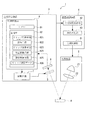
図1は、第一実施形態の分析装置である測色装置の概略構成を示すブロック図である。
図1において、測色装置1は、光源装置2と、分光測定装置3と、測色制御装置4と、を備えている。この測色装置1は、光源装置2から被検査対象Aに向かって例えば白色光を射出し、被検査対象Aで反射された光である検査対象光を分光測定装置3に入射させる。そして、分光測定装置3にて検査対象光を分光し、分光した各波長の光の光量をそれぞれ測定する分光特性測定を実施する。そして、測色制御装置4は、得られた分光特性に基づいて、被検査対象Aの測色処理、すなわちどの波長の色がどの程度含まれているかを分析する。
[First embodiment]
Hereinafter, a color measuring device which is an analyzer according to a first embodiment of the present invention will be described with reference to the drawings.
(1. Configuration of color measuring device)
FIG. 1 is a block diagram illustrating a schematic configuration of a color measurement device that is an analysis device of the first embodiment.
In FIG. 1, the
(2.光源装置の構成)
光源装置2は、光源21、複数のレンズ22(図1には1つのみ記載)を備え、被検査対象Aに対して白色光を射出する。また、複数のレンズ22には、コリメーターレンズが含まれており、光源装置2は、光源21から射出された白色光をコリメーターレンズにより平行光とし、図示しない投射レンズから被検査対象Aに向かって射出する。
(2. Configuration of light source device)
The
(3.分光測定装置の構成)
分光測定装置3は、被検査対象Aにより反射された測定対象光を分光し、分光された光の光量を測定することで、分光特性を得る装置である。この分光測定装置3は、図1に示すように、エタロン5と、受光手段としての受光部6と、駆動回路7と、制御回路部8と、を備えている。また、分光測定装置3は、エタロン5に対向する位置に、被検査対象Aで反射された反射光(測定対象光)を、内部に導光する図示しない入射光学レンズを備えている。
受光部6は、複数の光電交換素子により構成されており、受光量に応じた電気信号を生成する。そして、受光部6は、制御回路部8に接続されており、生成した電気信号を受光信号として制御回路部8に出力する。
(3. Configuration of spectrometer)
The
The light receiving unit 6 includes a plurality of photoelectric exchange elements, and generates an electrical signal corresponding to the amount of received light. The light receiving unit 6 is connected to the
(3−1.エタロンの構成)
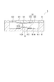
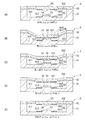
図2は、分光測定装置3を構成するエタロン5の概略構成を示す断面図である。
エタロン5は、例えば、平面視正方形状の板状の光学部材であり、一辺が例えば10mmに形成されている。このエタロン5は、図2に示すように、第一基板である可動基板52、および第二基板である固定基板51を備えている。これらの2枚の基板51,52は、それぞれ例えば、ソーダガラス、結晶性ガラス、石英ガラス、鉛ガラス、カリウムガラス、ホウケイ酸ガラス、無アルカリガラスなどの各種ガラスや、水晶などにより形成されている。これらの中でも、各基板51,52の構成材料としては、例えばナトリウム(Na)やカリウム(K)などのアルカリ金属を含有したガラスが好ましく、このようなガラスにより各基板51,52を形成することで、後述する反射膜53,54や、各電極の密着性や、基板同士の接合強度を向上させることが可能となる。そして、これらの2つの基板51,52は、例えば常温活性化接合などにより接合されることで、一体的に構成されている。
(3-1. Composition of etalon)
FIG. 2 is a cross-sectional view showing a schematic configuration of the
The
また、固定基板51と、可動基板52との間には、本発明の第二反射膜である固定反射膜53および第一反射膜である可動反射膜54が設けられる。ここで、固定反射膜53は、固定基板51の可動基板52に対向する面に固定され、可動反射膜54は、可動基板52の固定基板51に対向する面に固定されている。また、これらの固定反射膜53および可動反射膜54は、ギャップGを介して対向配置されている。
さらに、固定基板51と可動基板52との間には、固定反射膜53および可動反射膜54の間のギャップGの寸法を調整するためのギャップ調整手段としての静電アクチュエーター55が設けられている。
Further, between the fixed
Furthermore, an
(3−1−1.固定基板の構成)
固定基板51は、厚みが例えば500μmに形成されるガラス基材をエッチングにより加工することで形成される。具体的には、図3に示すように、固定基板51には、エッチングにより電極形成溝511および反射膜固定部512が形成される。
電極形成溝511は、例えば、エタロン5を厚み方向から見た平面視(以降、エタロン平面視と称す)において、円環形状に形成されている。反射膜固定部512は、前記平面視において、電極形成溝511の中心部に形成され、電極形成溝511の溝底面(電極固定面511A)から可動基板52側に突出して形成される。
そして、電極形成溝511の電極固定面511Aには、静電アクチュエーター55を構成する第一電極551が形成される。また、固定基板51には、電極固定面511Aに連続する図示しない第一電極引出溝が形成され、第一電極551の外周縁の一部から外側に向かって延出する図示しない第一電極引出部が形成されている。この第一電極引出部は、駆動回路7に接続されている。
(3-1-1. Configuration of Fixed Substrate)
The fixed
For example, the
A
反射膜固定部512は、上述したように、電極形成溝511と同軸上で、電極形成溝511よりも小さい径寸法となる円柱状に形成されている。なお、本実施形態では、図2に示すように、反射膜固定部512の可動基板52に対向する反射膜固定面512Aが、電極固定面511Aよりも可動基板52に近接して形成される例を示すが、これに限らない。電極固定面511Aおよび反射膜固定面512Aの高さ位置は、反射膜固定面512Aに固定される固定反射膜53、および可動基板52に形成される可動反射膜54の間のギャップGの寸法、第一電極551および可動基板52に形成される後述の第二電極552の間の寸法、固定反射膜53や可動反射膜54の厚み寸法により適宜設定されるものであり、上記のような構成に限られない。例えば反射膜53,54として、誘電体多層膜反射膜を用い、その厚み寸法が増大する場合、電極固定面511Aと反射膜固定面512Aとが同一面に形成される構成や、電極固定面511Aの中心部に、円柱凹溝上の反射膜固定溝が形成され、この反射膜固定溝の底面に反射膜固定面512Aが形成される構成などとしてもよい。
As described above, the reflection
そして、反射膜固定面512Aには、例えば直径が約3mmの円形状に形成される固定反射膜53が固定されている。この固定反射膜53は、AgC単層により形成される反射膜であり、スパッタリングなどの手法により反射膜固定面512Aに形成される。
なお、本実施形態では、固定反射膜53として、エタロン5で分光可能な波長域として可視光全域をカバーできるAgC単層の反射膜を用いる例を示すが、これに限定されず、例えば、エタロン5で分光可能な波長域が狭いが、AgC単層反射膜よりも、分光された光の透過率が大きく、透過率の半値幅も狭く分解能が良好な、例えばTiO2−SiO2系誘電体多層膜反射膜を用いる構成としてもよい。ただし、この場合、上述したように、固定基板51の反射膜固定面512Aや電極固定面511Aの高さ位置を、固定反射膜53や可動反射膜54、分光させる光の波長選択域などにより、適宜設定する必要がある。
A fixed
In the present embodiment, an example is shown in which an AgC single-layer reflective film that can cover the entire visible light region as a wavelength range that can be dispersed by the
さらに、固定基板51は、可動基板52に対向する上面とは反対側の下面において、固定反射膜53に対応する位置に図示略の反射防止膜(AR)が形成されている。この反射防止膜は、低屈折率膜および高屈折率膜を交互に積層することで形成され、固定基板51の表面での可視光の反射率を低下させ、透過率を増大させる。
Further, the fixed
(3−1−2.可動基板の構成)
可動基板52は、厚みが例えば200μmに形成されるガラス基材をエッチングにより加工することで形成される。
具体的には、可動基板52には、エタロン平面視において、基板中心点を中心とした円形の変位部521と、変位部521と同軸となる円環状に形成され変位部521の外周部に連結される連結保持部522と、を備えている。
(3-1-2. Configuration of movable substrate)
The
Specifically, the
変位部521は、連結保持部522よりも厚み寸法が大きく形成され、例えば、本実施形態では、可動基板52の厚み寸法と同一寸法である200μmに形成されている。また、変位部521は、反射膜固定部512の反射膜固定面512Aに平行な可動面521Aを備え、この可動面521Aに可動反射膜54が固定されている。ここで、この可動反射膜54と、上記した固定反射膜53とにより、本発明の一対の反射膜が構成される。また、本実施形態では、可動反射膜54と固定反射膜53との間のギャップGは、初期状態において、例えば450nmに設定されている。
ここで、この可動反射膜54は、上述した固定反射膜53と同一の構成の反射膜が用いられ、本実施形態では、AgC単層反射膜が用いられる。また、AgC単層反射膜の膜厚寸法は、例えば0.03μmに形成されている。
The
Here, as the movable
また、可動面521Aには、第一電極551に電磁ギャップを介して対向する、リング状の第二電極552が形成されている。ここで、この第二電極552および前述した第一電極551により静電アクチュエーター55が構成され、この静電アクチュエーター55と、駆動回路7と、により、本発明のギャップ調整手段が構成される。
また、第二電極552の外周縁の一部からは、図示しない第二電極引出部が外周方向に向かって形成され、駆動回路7に接続されている。そして、駆動回路7から出力される電圧により、第一電極551および第二電極552の間に静電引力が働き、変位部521が反射膜固定部512側に移動することで、ギャップGの間隔(ギャップ間隔)が調整される。
Further, a ring-shaped
A second electrode lead-out portion (not shown) is formed from a part of the outer peripheral edge of the
さらに、変位部521は、可動面521Aとは反対側の上面において、可動反射膜54に対応する位置に図示略の反射防止膜(AR)が形成されている。この反射防止膜は、固定基板51に形成される反射防止膜と同様の構成を有し、低屈折率膜および高屈折率膜を交互に積層することで形成される。
Further, the
連結保持部522は、変位部521の周囲を囲うダイアフラムであり、例えば厚み寸法が50μmに形成されている。また、連結保持部522は、弾性を有し、静電アクチュエーター55の静電引力により、変位部521が固定基板51側に移動すると、変位部521を初期位置に戻すように付勢力が働く。すなわち、連結保持部522は、本発明の付勢手段を構成する。
The
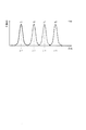
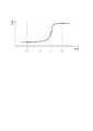
上述のようなエタロン5では、図3に示すような透過特性を有する。図3は、エタロン5の透過特性を示す図である。図3において、「Gap」はギャップ間隔を示す。
エタロン5では、一対に反射膜53,54の間のギャップGの間隔(ギャップ間隔)により、透過波長が決定される。すなわち、エタロン5を透過する光は、その半波長の整数倍がギャップ間隔と一致する光であり、半波長の整数倍がギャップ間隔と一致しない光は、反射膜53,54により反射される。したがって、図3に示すように、静電アクチュエーター55によりギャップ間隔をg0、g1、g2、g3と変化させることで、エタロン5を透過する光、すなわち透過率が大きい波長がλ0、λ1、λ2、λ3と変化する。
The
In the
(3−2.駆動回路の構成)
駆動回路7は、エタロン5の第一電極引出部、第二電極引出部、および制御回路部8に接続される。この駆動回路7は、制御回路部8から入力される駆動制御信号に基づいて、第一電極引出部および第二引出部を介して、第一電極551および第二電極552間に駆動電圧を印加し、変位部521を予め設定された第一変位位置まで移動させる。
(3-2. Configuration of drive circuit)
The
(3−3.制御回路部の構成)
制御回路部8は、分光測定装置3の全体動作を制御する。この制御回路部8は、図1に示すように、例えばCPU81、記憶部82などにより構成されている。そして、CPU81は、記憶部82に記憶された各種プログラム、各種データに基づいて、分光測定処理を実施する。記憶部82は、例えばメモリーやハードディスクなどの記録媒体を備えて構成され、各種プログラム、各種データなどを適宜読み出し可能に記憶する。
(3-3. Configuration of control circuit unit)
The
ここで、記憶部82には、プログラムとしては、ギャップ制御手段821、計時手段822、本発明のギャップ測定手段としてのギャップ演算手段823、光量認識手段824、および測定制御手段825が記憶されている。
また、記憶部82には、ギャップGの演算のためのギャップ演算データ826が記録されている。このギャップ演算データ826としては、静電アクチュエーター55に印加する電圧である初期駆動電圧、および初期駆動電圧を静電アクチュエーター55に印加した際のギャップ間隔である第一ギャップ間隔、変位部521が第一変位位置から初期位置まで戻るまでに要する所要復元時間が含まれる。ここで、初期駆動電圧を静電アクチュエーター55に印加した際の変位部521の変位位置(第一変位位置)が、本発明の設定変位位置となる。
このギャップ演算データ826は、例えばエタロン5の製造過程において測定されるデータであり、初期データとして記憶部82に記憶されている。すなわち、エタロン5の製造工程において、予め、初期駆動電圧を設定し、この初期駆動電圧を第一電極551および第二電極552間に印加した際の、ギャップ間隔(第一ギャップ間隔)を測定する。また、静電アクチュエーター55への電圧印加を停止し、変位部521が第一変位位置から初期位置に戻るまでの所要復元時間を測定する。そして、これらの初期駆動電圧、第一ギャップ間隔、所要復元時間が初期データであるギャップ演算データ826として予め記憶部82に記憶される。
なお、エタロン5の製造過程において、第一変位位置から所定時間経過後のギャップ間隔を予め測定して、復元経過時間とギャップ間隔とを関連付けたテーブルデータまたは、復元経過時間およびギャップ間隔の関係式などを、ギャップ演算データ826に含ませる構成としてもよい。
Here, the
Further,
The
In the manufacturing process of the
ギャップ制御手段821は、CPU81により読み出されることで実行されるプログラムであり、駆動回路7に駆動制御信号を出力して、静電アクチュエーター55を駆動させる。具体的には、ギャップ制御手段821は、記憶部82に記憶されているギャップ演算データ826から、初期駆動電圧を読み出し、この初期駆動電圧を静電アクチュエーター55に印加する旨の駆動制御信号を駆動回路7に出力する。
The gap control means 821 is a program executed by being read by the
計時手段822は、ギャップ制御手段821の制御により、変位部521が第一変位位置に移動した後、初期位置に戻るまでの復元過程の時間を計測する。具体的には、計時手段822は、ギャップ制御手段821によりエタロン5の静電アクチュエーター55に初期駆動電圧が印加された状態で、カウンターの値をリセットする。そして、ギャップ制御手段821の制御により、静電アクチュエーター55に印加される初期駆動電圧が切られた時点からの経過時間をカウントする。
The
ギャップ演算手段823は、変位部521が第一変位位置に移動された後、連結保持部522の復元力により初期位置に戻るまでの復元過程において、ギャップGの間隔を演算する。
ここで、変位部521は、第一変位位置に移動された後、静電アクチュエーター55への駆動電圧印加が停止、すなわち印加電圧が0Vに設定されると、変位部521には、連結保持部522の復元力のみが作用するため、次式(1)に示すような自由振動の挙動に沿って初期位置まで戻る。
The gap calculating means 823 calculates the gap G interval in the restoring process until the
Here, after the
[数1]
x=Asin(ωt+α) …(1)
[Equation 1]
x = Asin (ωt + α) (1)
ここで、変位部521の初期位置(変位部521が変位していない状態)に位置する際のギャップ間隔をg0とし、第一ギャップ間隔をg1とすると、A=g0−g1で求めることができる。また、変位部521が第一変位位置から初期位置までに要する所要復元時間をT1とすると、ω=2π/T=π/2T1となり、初期位相α=π/2となる。また、復元経過時間tが経過した後のギャップ間隔をgとすると、x=g0−gとなる。したがって、ギャップ間隔gは、次式(2)により求めることが可能となる。
Here, when the gap interval when the
[数2]
g=g0−(g0−g1)sin((2πt/T)+π/2) …(2)
[Equation 2]
g = g0− (g0−g1) sin ((2πt / T) + π / 2) (2)
したがって、変位部521が第一変位位置に移動した際の第一ギャップ間隔g1、第一変位位置から初期位置までに要する復元時間T1がギャップ演算データ826から取得できるため、第一変位位置から所定の復元経過時間が経過した後のギャップ間隔gを演算することができる。
Therefore, since the first gap interval g1 when the
光量認識手段824は、変位部521が第一変位位置に移動された後、連結保持部522の復元力により初期位置に戻るまでの復元過程において、受光部6から入力される電気信号(光量検出信号)を取得し、受光部6で測定された、エタロン5を透過した光の光量を認識する。
The light amount recognizing means 824 is an electric signal (light amount detection) input from the light receiving unit 6 in the restoration process after the
測定制御手段825は、ギャップ演算手段823によるギャップ間隔の演算と、光量認識手段824による透過光の受光量に応じた光量検出信号の認識と、を同時に実施させる制御(分光測定処理)をする。すなわち、測定制御手段825は、ギャップ間隔と、このギャップ間隔に対応して、受光部6で測定される透過光の受光量との双方を同時に取得する。
具体的には、測定制御手段825は、変位部521が第一変位位置に移動され、静電アクチュエーター55への初期駆動電圧の印加が停止された後、初期位置に戻るまでの復元過程において、分光測定処理を実施する。また、測定制御手段825は、計時手段で計測される復元経過時間と、この復元経過時間に対してギャップ演算手段823により演算されるギャップ間隔と、光量認識手段824により認識される光量検出信号と、を取得し、これらの復元経過時間、ギャップ間隔、および光量検出信号を関連付けて記憶部82に記憶する。
また、測定制御手段825は、復元過程において、この分光測定処置を複数回実施する。ここで、測定制御手段825が分光測定処理を実施するタイミングとしては、分光測定装置3により測定される分光特性の精度などにより適宜設定することが可能である。例えば、予め測定タイミングを設定しておき、記憶部82に記憶しておき、計時手段にて計時される復元経過時間がこの測定タイミングと一致した際に分光測定処理を実施する処理としてもよい。なお、本実施形態では、予め設定された周期で、計時手段により計時される復元経過時間、ギャップ演算手段823により測定されるギャップ間隔、光量測定手段により測定される透過光の光量を同時に取得する構成などとしてもよい。この場合、測定タイミングである周期を狭めることで、ギャップ間隔および透過光の光量の連続的な変化を監視でき、より精度の高い分光特性測定を実施することが可能となる。
The
Specifically, the
In addition, the measurement control means 825 performs this spectroscopic measurement treatment a plurality of times in the restoration process. Here, the timing at which the
(4.測色制御装置の構成)
測色制御装置4は、分光測定装置3および光源装置2に接続されており、光源装置2の制御、分光測定装置3により取得される分光特性に基づく測色処理を実施する。この測色制御装置4としては、例えば汎用パーソナルコンピューターや、携帯情報端末、その他、測色専用コンピューターなどを用いることができる。
そして、測色制御装置4は、図1に示すように、光源制御部41、分光特性取得部42、および測色処理部43などを備えて構成されている。
光源制御部41は、光源装置2に接続されている。そして、光源制御部41は、例えば利用者の設定入力に基づいて、光源装置2に所定の制御信号を出力し、光源装置2から所定の明るさの白色光を射出させる。
分光特性取得部42は、分光測定装置3に接続され、分光測定装置3から入力される分光特性を取得する。
(4. Configuration of colorimetric control device)
The color measurement control device 4 is connected to the
As shown in FIG. 1, the color measurement control device 4 includes a light
The light
The spectral characteristic acquisition unit 42 is connected to the
測色処理部43は、分光特性に基づいて、被検査対象Aの色度を測定する測色処理を実施する。例えば、測色処理部43は、分光測定装置3から得られた分光特性をグラフ化し、図示しないプリンターやディスプレイなどの出力装置に出力するなどの処理を実施する。
The
(5.分光測定装置の動作)
次に、上記のような測色装置1を構成する分光測定装置3の動作について図面に基づいて説明する。
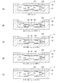
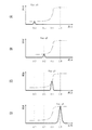
図4は、エタロン5における変位部521の変位状態を示す図であり、(A)は、静電アクチュエーター55に電圧が印加されていない初期状態を示す図、(B)は、静電アクチュエーター55に初期電圧V3を印加した状態を示す図、(C)は、復元過程において、復元経過時間t2が経過した状態を示す図、(D)は、復元経過時間t3(t3>t2)が経過した状態を示す図、(E)は、復元経過時間t4が経過し、変位部521が初期位置に復元された状態を示す図である。なお、図中「Gap」はギャップ間隔を示す。
図5は、分光測定装置3に入射する検査対象光の分光特性の例を示す図である。
図6は、図5に示す検査対象光がエタロン5に入射した際の、透過光の光量を示す図である。
図7は、図5に示す検査対象光に対して、受光部6から出力される光量検出信号を示す図である。
(5. Operation of spectrometer)
Next, the operation of the
4A and 4B are diagrams illustrating a displacement state of the
FIG. 5 is a diagram illustrating an example of the spectral characteristics of the inspection target light incident on the
FIG. 6 is a diagram illustrating the amount of transmitted light when the inspection target light illustrated in FIG. 5 is incident on the
FIG. 7 is a diagram illustrating a light amount detection signal output from the light receiving unit 6 with respect to the inspection target light illustrated in FIG.
上記のような分光測定装置3では、入射光(検査対象光)の分光特性を測定するために、まず、制御回路部8のCPU81は、記憶部82に記憶される各種プログラム、すなわち、ギャップ制御手段821、計時手段822、ギャップ演算手段823、光量認識手段824、および測定制御手段825を起動させる。
この後、CPU81により起動されたギャップ制御手段821は、記憶部82に記録されるギャップ演算データ826から初期駆動電圧を取得し、この初期駆動電圧を静電アクチュエーター55に印加する旨の駆動制御信号を駆動回路7に出力する。これにより、変位部521は、図4(A)に示すような初期位置から、図4(B)に示すような第一変位位置まで移動する。この時、ギャップ間隔は、ギャップ演算データ826に記憶される第一ギャップ間隔g3となる。
また、計時手段822は、変位部521が第一変位位置に移動したタイミングで、カウンター値をリセットし、例えば「0」に設定する。
In the
Thereafter, the gap control means 821 activated by the
Further, the time measuring means 822 resets the counter value at the timing when the
さらに、測定制御手段825は、変位部521が第一変位位置に位置する状態での分光測定処理を実施させる。つまり、測定制御手段825は、光量認識手段824を制御して、受光部6から出力される光量検出信号を認識させ、認識した光量検出信号を記憶部82に記憶する。なお、変位部521が第一変位位置に移動した状態でのギャップ間隔はギャップ演算データ826に記憶される第一ギャップ間隔g3であるため、ギャップ演算手段823によるギャップ間隔の演算は実施されない。
Further, the measurement control means 825 causes the spectroscopic measurement process in a state where the
この後、ギャップ制御手段821は、静電アクチュエーター55に印加していた初期駆動電圧V3を停止、すなわち静電アクチュエーター55への印加電圧を0Vに設定する。これにより、変位部521には、連結保持部522による付勢力のみが作用し、自由振動に挙動に従って初期位置まで復元する。
また、計時手段822は、ギャップ制御手段821により初期駆動電圧V3が停止されるタイミングt1をt1=0とし、以降、変位部521が初期位置に戻るまでの復元過程において、復元経過時間tをカウントする。
Thereafter, the gap control means 821 stops the initial drive voltage V3 applied to the
The time counting means 822 sets the timing t1 at which the initial drive voltage V3 is stopped by the gap control means 821 to t1 = 0, and thereafter counts the restoration elapsed time t in the restoration process until the
そして、測定制御手段825は、変位部521の復元過程において、計時手段822によりカウントされる復元経過時間tが予め設定された所定周期となる度に、ギャップ間隔gの演算および光量検出信号の取得を同時に行う分光測定処理を実施する。
なお、図4から図7では、計時手段822によりカウントされる復元経過時間tがt=t2、t3、t4となるタイミングでの分光測定処理を例示するが、実際には、さらに小さい周期に設定され、例えば略連続的に分光測定処理を実施し、略連続的に復元経過時間t、ギャップ間隔g、光量検出信号Iを取得する。
Then, the measurement control means 825 calculates the gap interval g and acquires the light amount detection signal every time the restoration elapsed time t counted by the time measuring means 822 reaches a predetermined period in the restoration process of the
4 to 7 exemplify the spectroscopic measurement process at the timing when the restoration elapsed time t counted by the time measuring means 822 becomes t = t2, t3, t4, but actually, it is set to a smaller cycle. For example, the spectroscopic measurement process is performed substantially continuously, and the restoration elapsed time t, the gap interval g, and the light amount detection signal I are acquired substantially continuously.
ここで、本実施形態では、復元経過時間tにより、ギャップ間隔gを演算し、このギャップ間隔gからさらに、透過光の波長を求める。すなわち、ギャップ演算手段823では、復元経過時間tを、上述した式(2)に代入することで、ギャップ間隔gが演算される。このギャップ間隔gが求まると、図3に示すように、エタロン5を透過する透過光の波長λが決定する。したがって、復元経過時間tでの透過光の光量を測定すれば、透過光の波長、およびこの波長に対する光量が測定できる。
例えば、図5に示すような検査対象光が分光測定装置3に入射し、図4(B)に示すように、変位部521が第一変位位置に位置する場合、ギャップ間隔がg3となる。この場合は、図6(A)に示すように、波長がλ3となる光のみ透過され、図7(A)に示すように、電流値I3が光量検出信号として出力される。
また、図4(C)(D)のように、復元経過時間tがt=t2,t3となる復元過程では、ギャップ演算手段823によりギャップ間隔g2、g1が演算される。この場合は、図6(B)(C)に示すように、波長がλ2、λ1となる光のみが透過され、図7(A)に示すように、電流値I2,I1が光量検出信号として出力される。
さらに、図4(E)に示すように、復元経過時間tがt=t4となり、変位部521が初期位置に戻った場合、ギャップ間隔がg0となる。このギャップ間隔g0は、予めギャップ演算データとして記録されているものを用いてもよいが、式(2)により演算により算出することで、より精度の高い測定が可能となる。この場合は、図6(D)に示すように、波長がλ0となる光のみが透過され、図7(A)に示すように、電流値I0が光量検出信号として出力される。
Here, in the present embodiment, the gap interval g is calculated from the restoration elapsed time t, and the wavelength of transmitted light is further obtained from the gap interval g. That is, the gap calculating means 823 calculates the gap interval g by substituting the restoration elapsed time t into the above-described equation (2). When the gap interval g is obtained, the wavelength λ of the transmitted light that passes through the
For example, when the inspection target light as shown in FIG. 5 enters the
Further, as shown in FIGS. 4C and 4D, in the restoration process in which the restoration elapsed time t is t = t2, t3, the gap intervals g2, g1 are calculated by the gap calculating means 823. In this case, as shown in FIGS. 6B and 6C, only light having wavelengths λ2 and λ1 is transmitted, and as shown in FIG. 7A, current values I2 and I1 are used as light quantity detection signals. Is output.
Further, as shown in FIG. 4E, when the restoration elapsed time t becomes t = t4 and the
そして、測定制御手段825による分光測定処理の測定タイミングをより小さい周期に設定することで、より詳細に波長に対する光量を検出することができ、例えば、連続的に復元経過時間tおよび光量検出信号Iを取得することで、図7(B)に示すような分光特性曲線を得ることができる。なお、測定回数が少ない場合、例えば図7(A)に示すような測定結果が得られた場合、これらの測定結果を補完処理することで、図7(B)のような分光特性曲線を得る構成としてもよい。 Then, by setting the measurement timing of the spectroscopic measurement processing by the measurement control means 825 to a smaller period, the light quantity with respect to the wavelength can be detected in more detail. For example, the restoration elapsed time t and the light quantity detection signal I can be continuously detected. Is obtained, a spectral characteristic curve as shown in FIG. 7B can be obtained. When the number of times of measurement is small, for example, when measurement results as shown in FIG. 7A are obtained, a spectral characteristic curve as shown in FIG. 7B is obtained by complementing these measurement results. It is good also as a structure.
(6.第一実施形態の作用効果)
上述したように、上記第一実施形態の測色装置1における分光測定装置3では、ギャップ制御手段821により、駆動回路7から静電アクチュエーター55に初期駆動電圧を印加して、エタロン5の変位部521を第一変位位置まで移動させた後、静電アクチュエーター55への電圧印加を停止させる。そして、測定制御手段825は、変位部521が初期位置に復元するまでの復元過程で、分光測定処理を実施し、すなわち、ギャップ演算手段823によるギャップ間隔の測定、および光量認識手段824による光量測定を実施させる。
(6. Effects of First Embodiment)
As described above, in the
このため、復元過程において、一対の反射膜53,54間のギャップ間隔を正確に求めることができ、受光部6で受光される透過光の正確な波長を求めることができる。
ここで、静電アクチュエーター55に電圧を印加してギャップ間隔を所望の値に設定する場合では、第一電極551および第二電極552の膜厚、一対の反射膜53,54の膜厚などにより、個々のエタロン5により個体差が生じ、所望のギャップ間隔に設定することが困難となる。また、複数回のフィードバック制御を繰り返すような制御を実施する場合では、ギャップ間隔の調整処理に長時間を要する場合がある。これに対して、上記実施形態の分光測定装置3では、復元過程で、ギャップ間隔を測定するだけで、透過光の波長を求めることができ、迅速な分光測定処理を実施できる。
また、ギャップ測定と同時に光量測定を実施するため、上記のように、求めた正確な波長に対する光量を得ることができる。したがって、ギャップ演算手段823によるギャップ測定処理のタイミングを変化させることで、異なる波長の透過光の光量を検出することができる。そして、このように測定された複数波長に対する光量を求めることで、検査対象光の正確な分光特性を取得することができる。
また、このような分光測定装置3を備えた測色装置1では、迅速にかつ精度の高い分光特性に基づいた測色処理を実施できる。
For this reason, in the restoration process, the gap interval between the pair of
Here, when a voltage is applied to the
Further, since the light amount measurement is performed simultaneously with the gap measurement, the light amount with respect to the obtained accurate wavelength can be obtained as described above. Therefore, the amount of transmitted light having different wavelengths can be detected by changing the timing of the gap measurement processing by the gap calculating means 823. And the exact spectral characteristic of inspection object light is acquirable by calculating | requiring the light quantity with respect to the several wavelength measured in this way.
In addition, the
また、上記のような分光測定装置3では、測定制御手段825は、復元過程において、複数回の分光測定処理を実施する。このため、例えば1度の復元過程で1回の分光測定処理を実施する場合では、検査対象光の分光特性を得るために複数回測定を実施する必要があるが、1度の復元過程で複数の測定結果が得られるため、測定回数を減らすことができる。したがって、検査対象光の分光特性をより迅速に測定することができる。
これに加えて、本実施形態では、測定制御手段825により分光測定処理を実施するタイミング周期を小さく設定し、略連続的に分光測定処理を実施する。したがって、一度の測定で、エタロン5により分光可能な波長域の全域に対して、その分光特性を得ることができ、図7(B)に示すような精度の高い分光特性曲線を得ることができる。
In the
In addition to this, in the present embodiment, the
さらに、ギャップ演算手段823は、復元経過時間tに基づいて、式(2)によりギャップ間隔を演算により求めている。このため、ギャップ演算手段823は、計時手段822により計測される復元経過時間を取得することで、容易にギャップ間隔を演算により求めることができる。このような構成では、ギャップ間隔を測定するために、エタロン5に特別な構成部品を設ける必要がなく、エタロン5の構成を簡単にできる。
Further, the gap calculating means 823 calculates the gap interval by calculation based on the restoration elapsed time t using equation (2). For this reason, the
そして、測定制御手段825により分光測定処理を実施する際に、ギャップ制御手段821は、静電アクチュエーター55に印加する電圧を0Vに設定する。このため、変位部521には、静電アクチュエーター55による静電引力が作用しない。したがって、変位部521は、連結保持部522の付勢力(復元力)による自由振動の挙動にしたがって初期位置まで復元し、ギャップ演算手段823は、式(2)に示すような簡単な演算式で正確なギャップ間隔を求めることができる。
When the spectroscopic measurement process is performed by the
また、ギャップ制御手段821、計時手段822、ギャップ演算手段823、光量認識手段824、および測定制御手段825は、記憶部82に記憶されるプログラムにより構成され、CPU81により適宜読み出されて実行されることで、分光特性の測定処理が実施される。このような構成とすることで、構造の簡略化を図れ、分光測定装置3の小型化にも対応できる。
Further, the
〔第二実施形態〕
次に、本発明に係る第二実施形態の測色装置について、図面に基づいて説明する。
図8は、第二実施形態の測色装置の概略構成を示すブロック図である。図8において、前記第一実施形態と同様の構成については、同符号を付し、その説明を省略または簡略する。
[Second Embodiment]
Next, a color measuring device according to a second embodiment of the present invention will be described with reference to the drawings.
FIG. 8 is a block diagram illustrating a schematic configuration of the color measurement device according to the second embodiment. In FIG. 8, the same components as those in the first embodiment are denoted by the same reference numerals, and the description thereof is omitted or simplified.
第二実施形態の測色装置1は、第一実施形態と略同様の構成を有し、分光測定装置3の一部の構成のみが異なる。
すなわち、第二実施形態の分光測定装置3は、エタロン5と、受光手段としての受光部6と、駆動回路7と、ギャップ検出回路9と、制御回路部8と、を備えている。この第二実施形態では、エタロン5を構成する第一電極551、第二電極552、およびギャップ検出回路9により本発明のギャップ検出手段が構成される。
また、制御回路部8は、CPU81と記憶部82とを備え、記憶部82には、CPU81により読み出されて実行されるプログラムとして、ギャップ制御手段821、計時手段822、ギャップ認識手段827、光量認識手段824、および測定制御手段825が記録されている。
ここで、エタロン5の構成、受光部6、駆動回路7の構成については、上記第一実施形態と同様の構成であるため、ここでの説明は省略する。
The
That is, the
In addition, the
Here, since the configuration of the
ギャップ検出回路9は、エタロン5の静電アクチュエーター55である第一電極551および第二電極552に接続されている。すなわち、第二実施形態では、第一電極551および第二電極552は、本発明の静電容量測定用電極としても機能する。
ここで、図9にエタロン5の平面図を示す。図9に示すように、第二実施形態のエタロン5は、平面視正方形状に形成されるが、第一電極551から対角関係となる頂点5A,5Cに向かって、それぞれ、駆動用第一電極引出部551A、および検出用第一電極引出部551Bが形成される。同様にして、第二電極552から対角関係となる頂点5B,5Dに向かって、駆動用第二電極引出部552A、および検出用第二電極引出部552Bが形成される。そして、駆動用第一電極引出部551Aの先端部、および駆動用第二電極引出部552Aの先端部は、それぞれ駆動回路7に接続され、検出用第一電極引出部551Bの先端部、および検出用第二電極引出部552Bの先端部は、それぞれギャップ検出回路9に接続される。
なお、第一電極551および第二電極552は、それぞれ1つずつ引出部を備え、これらの引出部に駆動回路7およびギャップ検出回路9の双方が接続される構成であってもよい。ただし、本実施形態のように、エタロン5が、一辺10mm程度に形成される微小基板により構成される場合、1つの引出部に駆動回路7およびギャップ検出回路9を接続する構成では、配線作業が困難となるおそれがある。また、ギャップ検出回路9に、駆動回路7による電圧印加のノイズが入りやすくなるなどの問題もある。したがって、図9に示すように、第一電極551に、駆動用第一電極引出部551A、および検出用第一電極引出部551Bの双方を形成し、第二電極552に駆動用第二電極引出部552A、および検出用第二電極引出部552Bの双方を形成する構成とすることが好ましい。
The gap detection circuit 9 is connected to the
Here, a plan view of the
Note that the
そして、ギャップ検出回路9は、検出用第一電極引出部551Bおよび検出用第二電極引出部552Bから第一電極551および第二電極552に保持されている電荷の保持量を検出する。また、ギャップ検出回路9は、これらの電荷保持量に基づいて、ギャップ間隔を算出し、ギャップ検出信号として制御回路部に出力する。
The gap detection circuit 9 detects the amount of charge held in the
制御回路部8は、第一実施形態と同様に、分光測定装置3の全体動作を制御する。この制御回路部8は、図8に示すように、例えばCPU81、記憶部82などにより構成されている。そして、CPU81は、記憶部82に記憶された各種プログラム、各種データに基づいて、分光測定処理を実施する。記憶部82は、例えばメモリーやハードディスクなどの記録媒体を備えて構成され、各種プログラム、各種データなどを適宜読み出し可能に記憶する。
The
ここで、記憶部82には、プログラムとしては、ギャップ制御手段821、計時手段822、ギャップ認識手段827、光量認識手段824、および測定制御手段825が記憶されている。
また、記憶部82には、ギャップGの演算のためのギャップ演算データ826が記録され、このギャップ演算データ826には、静電アクチュエーター55に印加する電圧である初期駆動電圧が記録される。
なお、計時手段822および光量認識手段824については、第一実施形態と同様の構成であり、CPU81により実行されることで同様の動作を実施するため、ここでの説明は省略する。
Here, the
Further,
Note that the
ギャップ制御手段821は、CPU81により読み出されることで実行されるプログラムであり、駆動回路7に駆動制御信号を出力して、静電アクチュエーター55を駆動させる。
ここで、第二実施形態のギャップ制御手段821は、静電アクチュエーター55に初期駆動電圧を印加することで、可動反射膜54と固定反射膜53とが当接する、すなわちギャップ間隔が0となる限界変位位置まで、変位部521を移動させる。
この時、各反射膜53,54に過剰な応力が加わり、膜の平行関係が崩れたりする不都合を防止するために、エタロン5の製造時に、変位部521を限界変位位置に移動させるために必要な最低電圧が測定され、初期駆動電圧としてギャップ演算データ826に記憶される。なお、各反射膜53,54の外周縁に膜厚と同一突出寸法の移動規制部を設け、ギャップ制御手段821は、これらの移動規制部が当接する位置まで変位部521を移動させる構成などとしてもよい。
The gap control means 821 is a program executed by being read by the
Here, the gap control means 821 of the second embodiment applies the initial drive voltage to the
At this time, it is necessary to move the
ギャップ認識手段827は、ギャップ検出回路9から入力されるギャップ検出信号に基づいて、ギャップ間隔を認識する。また、ギャップ認識手段827は、認識したギャップ間隔を、復元経過時間t、および光量認識手段824により認識される光量(光量検出信号)とともに、記憶部82に記録する。
The
測定制御手段825は、第一実施形態と略同様の構成であり、ギャップ間隔と、このギャップ間隔に対応して、受光部6で測定される透過光の受光量との双方を同時に取得する。ここで、測定制御手段825は、ギャップ認識手段827により認識されるギャップ間隔と、光量認識手段824による透過光の受光量に応じた光量検出信号の認識と、を同時に実施させる制御(分光測定処理)をする。
The
次に、上記のような分光測定装置3の動作について図面に基づいて説明する。
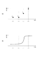
図10は、第二実施形態におけるエタロン5の変位部521の変位位置を示す図であり、(A)は、静電アクチュエーター55に電圧が印加されていない初期状態を示す図、(B)は、静電アクチュエーター55に初期電圧V4を印加した状態を示す図、(C)は、復元過程において、復元経過時間t2が経過した状態を示す図、(D)は、復元経過時間t3(t3>t2)が経過した状態を示す図、(E)は、復元経過時間t4が経過し、変位部521が初期位置に復元された状態を示す図である。なお、図中「Gap」はギャップ間隔を示す。
Next, the operation of the
10A and 10B are diagrams showing the displacement position of the
上記のような分光測定装置3では、入射光(検査対象光)の分光特性を測定するために、まず、制御回路部8のCPU81は、記憶部82に記憶される各種プログラム、すなわち、ギャップ制御手段821、計時手段822、ギャップ認識手段827、光量認識手段824、および測定制御手段825を起動させる。
この後、CPU81により起動されたギャップ制御手段821は、記憶部82に記録されるギャップ演算データ826から初期駆動電圧V4を取得し、この初期駆動電圧V4を静電アクチュエーター55に印加する旨の駆動制御信号を駆動回路7に出力する。これにより、変位部521は、図10(A)に示すような初期位置から、図10(B)に示すような限界変位位置まで移動し、ギャップ間隔が0に設定される。なお、変位部521を限界変位位置に移動させた場合においても、第一電極551および第二電極552の間には所定の電磁ギャップが形成され、電荷が逃げることがない。
また、計時手段822は、変位部521が第一変位位置に移動したタイミングで、カウンター値をリセットし、例えば「0」に設定する。
In the
Thereafter, the gap control means 821 activated by the
Further, the time measuring means 822 resets the counter value at the timing when the
さらに、測定制御手段825は、変位部521が限界変位位置に位置する状態での分光測定処理を実施させる。すなわち、測定制御手段825は、光量認識手段824を制御して、受光部6から出力される光量検出信号を認識させ、認識した光量検出信号を記憶部82に記憶する。なお、変位部521が限界変位位置に移動した状態では、ギャップ間隔が0となるため、ギャップ検出回路9によるギャップ間隔の測定は実施しなくてもよい。
Further, the measurement control means 825 causes the spectroscopic measurement process in a state where the
この後、ギャップ制御手段821は、静電アクチュエーター55に印加していた初期駆動電圧V4を停止する。これにより、変位部521には、連結保持部522による付勢力のみが作用し、自由振動に挙動に従って初期位置まで復元する。
また、計時手段822は、ギャップ制御手段821により初期駆動電圧V4が停止されるタイミングt1をt1=0としてカウントし、以降、変位部521が初期位置に戻るまでの復元過程において、復元経過時間tをカウントする。
Thereafter, the gap control means 821 stops the initial drive voltage V4 applied to the
Further, the time counting means 822 counts the timing t1 at which the initial drive voltage V4 is stopped by the gap control means 821 as t1 = 0, and thereafter, in the restoration process until the
そして、測定制御手段825は、変位部521の復元過程において、計時手段822によりカウントされる復元経過時間tを監視し、予め設定された一定周期毎に、ギャップ検出回路9によるギャップ間隔の測定および光量検出信号の取得を同時に行う分光測定処理を実施する。
Then, the measurement control means 825 monitors the restoration elapsed time t counted by the time measuring means 822 in the restoration process of the
ここで、第二実施形態では、ギャップ検出回路9により、ギャップ間隔gを測定する。また、第一実施形態と同様に、ギャップ間隔gが測定されると、このギャップ間隔gから透過光の波長を求めることができる。したがって、上記のように、復元経過時間tにおけるギャップ間隔gと、透過光の光量に基づいた光量検出信号を測定すれば、透過光の波長に対する光量を測定できる。 Here, in the second embodiment, the gap interval g is measured by the gap detection circuit 9. Similarly to the first embodiment, when the gap interval g is measured, the wavelength of transmitted light can be obtained from the gap interval g. Therefore, as described above, if the light amount detection signal based on the gap interval g at the restoration elapsed time t and the light amount of the transmitted light is measured, the light amount with respect to the wavelength of the transmitted light can be measured.
そして、第一実施形態と同様に、測定制御手段825による分光測定処理の測定タイミングをより小さい周期に設定することで、より詳細に波長に対する光量を検出することができ、例えば、連続的にギャップ間隔gおよび光量検出信号Iを取得することで、図7(B)に示すような分光特性曲線を得ることができる。 As in the first embodiment, the light intensity with respect to the wavelength can be detected in more detail by setting the measurement timing of the spectroscopic measurement processing by the measurement control means 825 to a smaller period, for example, a gap continuously. By obtaining the interval g and the light amount detection signal I, a spectral characteristic curve as shown in FIG. 7B can be obtained.
(第二実施形態の作用効果)
上述した第二実施形態では、上記第一実施形態の作用効果に加えて次のような効果が得られる。
第二実施形態の測色装置1における分光測定装置3では、ギャップ検出回路9により、静電アクチュエーター55の第一電極551および第二電極552に保持される電荷量を検出して、ギャップ間隔gを測定する。このような構成では、各電極551,552に保持される電荷量に基づいたより正確なギャップ間隔を測定することができる。
すなわち、変位部521を連結保持部522の復元力により初期位置に復元させる場合、自由振動の挙動にほぼ従い、上記第一実施形態に示すギャップ演算手段823により、式(2)に基づいて正確なギャップ間隔を算出することができる。しかしながら、厳密には、変位部521は、振動幅が減衰し、最終的には初期位置で静止する、いわゆる減衰自由振動となる。ここで、ギャップ演算手段823により、減衰自由振動の挙動に基づいた演算式を用い、ギャップ間隔gを計算することで、より精密なギャップ間隔を算出することは可能であるが、この場合、演算式が複雑となり、処理時間や処理負荷も増大する。これに対して、ギャップ検出回路9により静電容量に基づいたギャップ間隔の測定では、第一電極551および第二電極552の静電容量を検出することで容易に、かつ迅速に、より正確なギャップ間隔を求めることができる。
したがって、より正確なギャップ間隔に基づいて、エタロン5を透過する光の波長を算出することができるため、分光特性の測定精度もより向上させることができる。
(Operational effects of the second embodiment)
In the second embodiment described above, the following effects are obtained in addition to the operational effects of the first embodiment.
In the
That is, when the
Therefore, since the wavelength of light transmitted through the
また、ギャップ検出回路9は、静電アクチュエーター55を構成する第一電極551および第二電極552の電荷保持量を検出する。したがって、ギャップ間隔の測定用に別途電極を設ける必要がなく、エタロン5の変位部521を駆動させるための静電アクチュエーター55の構成を、そのままギャップ間隔の測定用の電極として用いることができる。これにより、エタロン5の構成が複雑化せず、簡単な構成でギャップ間隔を測定することができる。
Further, the gap detection circuit 9 detects the charge retention amounts of the
また、測定制御手段825により分光測定処理を実施する際に、ギャップ制御手段821は、静電アクチュエーター55に印加する電圧を0Vに設定する。このため、ギャップ検出回路9に、駆動電圧のノイズが入らず、正確なギャップ間隔の測定を実施することができる。
Further, when the spectroscopic measurement process is performed by the
〔変形例〕
なお、本発明は前述の実施形態に限定されるものではなく、本発明の目的を達成できる範囲での変形、改良等は本発明に含まれるものである。
例えば、第一実施形態において、ギャップ制御手段821は、初期駆動電圧V3を静電アクチュエーター55に印加し、変位部521を第一変位位置まで移動させたが、これに限定されない。例えば、第二実施形態のように、静電アクチュエーター55に初期駆動電圧V4を印加し、変位部521を限界変位位置まで変位させたのち、復元過程での分光測定処理を実施してもよい。同様に、第二実施形態において、ギャップ制御手段821は、静電アクチュエーター55に初期駆動電圧V3を印加し、変位部521を第一変位位置に移動させる構成としてもよい。
[Modification]
It should be noted that the present invention is not limited to the above-described embodiments, and modifications, improvements, and the like within the scope that can achieve the object of the present invention are included in the present invention.
For example, in the first embodiment, the
また、変位部521を変位させるギャップ調整手段として、上記第一および第二実施形態では、第一電極551および第二電極552により構成される静電アクチュエーター55と、駆動回路7とを備える構成としたが、これに限定されない。例えば、変位部521と固定基板51とを圧電体により連結し、圧電体に電圧を印加し、伸縮させることでギャップ間隔を調整する構成としてもよい。
第二実施形態では、ギャップ検出回路9により静電アクチュエーター55に保持される電荷保持量を検出したが、上記のような圧電体を用いた構成とする場合、圧電体の変形により発生する電流によりギャップ間隔を検出することができる。
Further, as the gap adjusting means for displacing the
In the second embodiment, the amount of electric charge held by the
さらに、第一および第二実施形態において、第二電極552が変位部521の可動反射膜の外周側に形成される例を示したが、例えば、連結保持部522に設けられる構成などとしてもよい。また、可動基板52に第二電極形成用の溝を形成する構成としてもよい。さらに、第一電極551および第二電極552が円環状に形成される例を示したが、これに限定されず、反射膜を挟む位置にそれぞれ電極が形成されていれば、変位部521を固定基板51に対して平行に変位させることができる。
Further, in the first and second embodiments, the example in which the
また、第一実施形態において、復元過程において、ギャップ制御手段821は、静電アクチュエーター55への駆動電圧を停止し、連結保持部522の復元力により変位部521を初期位置まで戻したが、例えば、復元過程において、静電アクチュエーター55に印加する電圧を制御して、変位部521を例えば等速で初期位置まで移動させる構成などとしてもよい。この場合、変位部521を等速に維持するための静電アクチュエーター55への印加電圧制御が複雑となるが、分光測定処理を一定周期で複数回実施する場合、複数の測定で得られるギャップ間隔の変動量を同じにできる。すなわち、第一変位位置から初期位置までを自由振動で変位する変位部521に対して、第一変位位置および初期位置近傍では、変位部の速度が遅く、中間位置では変位部の速度が速くなる。このため、エタロン5により分光可能な波長域において、高波長域側および低波長域側に対する光量の測定結果が多く得られ、中間波長域における測定結果が少なくなる。これに対して、上記のように等速で変位部を移動させた場合、全波長域に対して同等の測定結果が得られ、より正確な分光特性測定を実施できる。なお、変位部521が自由振動の挙動に従って変位する場合であっても、上述したように、分光測定処理を実施する周期を短くして、例えば連続的にギャップ間隔と光量検出とを実施することで、正確な分光特性曲線を得ることができる。
In the first embodiment, in the restoration process, the
また、上記第一および第二実施形態では、計時手段822は、ギャップ制御手段821により、静電アクチュエーター55への初期駆動電圧の印加が停止されるタイミングを0として、復元経過時間を計測するとしたが、例えば、ギャップ制御手段821による初期駆動電圧の印加タイミングから時間を計測するものであってもよい。この場合であっても、初期駆動電圧が停止されるタイミングが計測されていれば、復元経過時間を容易に算出することができ、上記実施形態と同様の処理により、分光測定処理を実施できる。
In the first and second embodiments, the
さらに、上記第二実施形態において、静電アクチュエーター55を構成する第一電極551及び第二電極552を、ギャップ検出回路9に接続し、本発明の静電容量測定用電極としても機能させる構成としたが、これに限定されない。例えば、ギャップ調整手段を構成する静電アクチュエーター55の第一電極551、第二電極552とは別に、一対の静電測定用電極を変位部521および固定基板51に設ける構成としてもよい。この場合、構成が複雑化するが、駆動回路7からの電流を確実に遮断することができ、例えばリーク電流などにより誤差も発生しない。したがって、より信頼性の高いギャップ間隔の測定が実施でき、より信頼性の高い分光特性の測定を実施できる。
Furthermore, in the second embodiment, the
また、復元過程における分光測定処理の回数としては、上記実施形態のように、連続的に分光測定処理を実施するものであってもよく、より大きい周期で分光測定処理を実施するものであってもよい。また、1度の復元過程において1回の分光測定処理を実施してもよい。さらに、予め設定された復元経過時間において、分光測定処理を実施してもよい。 Further, the number of times of the spectroscopic measurement process in the restoration process may be such that the spectroscopic measurement process is continuously performed as in the above-described embodiment, and the spectroscopic measurement process is performed with a larger period. Also good. In addition, one spectroscopic measurement process may be performed in one restoration process. Further, the spectroscopic measurement process may be performed during a preset restoration elapsed time.
そして、第一および第二実施形態では、変位部521が第一基板である可動基板にのみ形成される例を示したが、例えば、固定基板51の反射膜固定部512も変位可能な構成としてもよい。
また、付勢手段として、ダイアフラム状の連結保持部522を例示したが、例えば変位部521の外周縁から径外方向に延びる複数の保持軸が形成され保持軸の弾性力により付勢力が付与される構成などとしてもよく、固定基板51および可動基板52の間に、弾性部材を配置し、変位部521を初期位置まで押し上げる構成などとしてもよい。
In the first and second embodiments, the example in which the
Further, the diaphragm-like
第一および第二実施形態において、エタロン5を透過する光を受光部6により受光する構成としたがこれに限定されない。例えば、エタロン5により反射される光を受光部により受光する構成などとしてもよい。
In 1st and 2nd embodiment, although it was set as the structure which receives the light which permeate | transmits the
さらに、測色装置1は、被検査対象Aに光を照射する光源装置2を備える例を示したが、例えば、自ら光を発するディスプレイなどの表示装置を被検査対象Aとする場合などでは、光源装置2が設けられない構成としてもよい。
さらには、光源装置2から射出された光が被検査対象Aに反射され、この反射光を分光測定装置3により測定する構成を例示したが、例えば、エタロン5を透過した光を被検査対象Aにて反射させ、受光部6により受光させる構成などとしてもよい。
Furthermore, although the
Furthermore, although the light emitted from the
また、上記第一および第二実施形態において、ギャップ制御手段821、計時手段、ギャップ演算手段823、ギャップ認識手段827、光量認識手段824、および測定制御手段825は、記憶部82に記憶されるプログラムであり、CPU81により読み出されることで実行されるソフトウェアとしての構成例を示したが、これに限定されない。例えば、ICなどの集積回路などによりハードウェアとして構成されるものであってもよい。
In the first and second embodiments, the
また、上記第一および第二実施形態では、本発明の分析装置として、検査対象光の色度を測定する測色装置1を例示するが、これに限定されない。すなわち、分析装置としては、例えば、ガス特有の吸収波長を検出することでガス検出を実施するガスセンサーなどにも適用することができる。ここで、分光測定装置3では、エタロン5における一対の反射膜53,54間のギャップGの間隔が正確に求めることができ、このギャップ間隔に対する透過光の光量が得られる。すなわち、分光測定装置3から分析装置に正確な分光特性が出力されるため、分析装置での分光特性を用いた分析処理においても、正確な処理を実施することができる。
In the first and second embodiments, the
1…分析装置としての測色装置、3…分光測定装置、5…エタロン、6…受光手段である受光部、7…ギャップ調整手段の一部を構成する駆動回路、9…ギャップ測定手段の一部を構成するギャップ検出回路、51…第二基板である固定基板、52…第一基板である可動基板、53…第二反射膜である固定反射膜、54…第一反射膜である可動反射膜、55…ギャップ調整手段の一部およびギャップ測定手段の一部を構成する静電アクチュエーター、551…静電駆動電極および静電容量測定用電極である第一電極、552…静電駆動電極および静電容量測定用電極である第二電極、521…変位部、522…付勢手段である連結保持部、821…ギャップ制御手段、823…ギャップ測定手段であるギャップ演算手段、825…測定制御手段。
DESCRIPTION OF
Claims (8)
前記第一基板に設けられ、基板厚み方向に沿って変位可能な変位部と、
前記変位部を、当該変位部が変位していない位置である初期位置に向かって付勢する付勢手段と、
前記第一基板の前記変位部に設けられる第一反射膜と、
前記第二基板に設けられ、ギャップを介して前記第一反射膜に対向する第二反射膜と、
前記ギャップの間隔を変化させるギャップ調整手段と、
前記ギャップの間隔を測定するギャップ測定手段と、
前記第一反射膜および第二反射膜を透過または反射した光を受光するとともに、受光量を測定する受光手段と、
前記ギャップ調整手段を制御し、前記変位部を予め設定された設定変位位置まで変位させるギャップ制御手段と、
前記変位部が前記設定変位位置から前記初期位置に戻る復元過程で、前記受光手段による受光量の測定、およびギャップ測定手段によるギャップの間隔の測定を同時に実施させる測定制御手段と、
を具備したことを特徴とする分光測定装置。 A first substrate and a second substrate facing each other;
A displacement portion provided on the first substrate and displaceable along the substrate thickness direction;
An urging means for urging the displacement portion toward an initial position where the displacement portion is not displaced;
A first reflective film provided on the displacement portion of the first substrate;
A second reflective film provided on the second substrate and facing the first reflective film via a gap;
Gap adjusting means for changing the gap interval;
Gap measuring means for measuring the gap interval;
A light receiving means for receiving light transmitted through or reflected by the first reflective film and the second reflective film, and measuring the amount of received light;
Gap control means for controlling the gap adjusting means and displacing the displacement portion to a preset set displacement position;
A measurement control means for simultaneously performing the measurement of the amount of light received by the light receiving means and the measurement of the gap interval by the gap measuring means in the restoration process in which the displacement portion returns from the set displacement position to the initial position;
A spectroscopic measurement device comprising:
前記測定制御手段は、前記復元過程において、前記受光手段による前記受光量の測定、および前記ギャップ測定手段による前記ギャップの間隔の測定を同時に、かつ複数回実施させる
ことを特徴とする分光測定装置。 The spectroscopic measurement device according to claim 1,
In the restoration process, the measurement control unit causes the measurement of the amount of received light by the light receiving unit and the measurement of the gap interval by the gap measuring unit simultaneously and a plurality of times.
前記ギャップ測定手段は、前記変位部および前記第二基板の前記変位部に対向する面に対向配置される一対の静電容量測定用電極を備える
ことを特徴とする分光測定装置。 The spectroscopic measurement device according to claim 1 or 2,
The spectroscopic measurement apparatus, wherein the gap measuring means includes a pair of capacitance measuring electrodes disposed to face the displacement portion and a surface of the second substrate facing the displacement portion.
前記ギャップ測定手段は、前記変位部が、前記設定変位位置から、前記設定変位位置および前記初期位置の間の中間変位位置に移動するまでの時間に基づいて、前記ギャップの間隔を測定する
ことを特徴とする分光測定装置。 The spectroscopic measurement device according to claim 1 or 2,
The gap measuring means measures the gap interval based on a time until the displacement unit moves from the set displacement position to an intermediate displacement position between the set displacement position and the initial position. A spectroscopic measurement device.
前記ギャップ調整手段は、前記変位部および前記第二基板の前記変位部に対向する面に対向配置される一対の静電駆動電極を備え、これらの前記静電駆動電極に電圧が印加されることで、静電引力により前記変位部を変位させ、
前記静電容量測定用電極は、前記静電駆動電極であり、
前記ギャップ測定手段は、前記静電駆動電極に保持される電荷に基づいて、前記ギャップの間隔を測定する
ことを特徴とする分光測定装置。 The spectrometer according to claim 3,
The gap adjusting means includes a pair of electrostatic drive electrodes arranged to face the displacement portion and a surface of the second substrate facing the displacement portion, and a voltage is applied to the electrostatic drive electrodes. Then, the displacement part is displaced by electrostatic attraction,
The capacitance measuring electrode is the electrostatic drive electrode,
The gap measuring means measures the gap interval based on the electric charge held on the electrostatic drive electrode.
前記ギャップ調整手段は、前記第一基板および前記第二基板の互いに対向する面に設けられる静電駆動電極を備え、
前記ギャップ制御手段は、前記変位部を前記設定変位位置に変位させる際に前記静電駆動電極に電圧を印加し、前記復元過程において、前記静電駆動電極への電圧印加を停止させる
ことを特徴とする分光測定装置。 The spectrometer according to any one of claims 1 to 5,
The gap adjusting means includes electrostatic drive electrodes provided on surfaces of the first substrate and the second substrate facing each other,
The gap control means applies a voltage to the electrostatic drive electrode when displacing the displacement portion to the set displacement position, and stops applying the voltage to the electrostatic drive electrode in the restoration process. A spectroscopic measurement device.
前記設定変位位置は、前記第一反射膜および前記第二反射膜が当接する限界変位位置である
ことを特徴とする分光測定装置。 The spectrometer according to any one of claims 1 to 6,
The spectroscopic measurement apparatus, wherein the set displacement position is a limit displacement position where the first reflective film and the second reflective film are in contact with each other.
前記分光測定装置での測定処理により得られる、前記ギャップの間隔に対する前記受光量に基づいて、測定対象光の分光特性を分析する分析手段と、
を備えることを特徴とした分析装置。 A spectroscopic measurement device according to any one of claims 1 to 7,
Analyzing means for analyzing the spectral characteristics of the light to be measured based on the amount of received light with respect to the gap interval, obtained by the measurement process in the spectrometer,
An analyzer characterized by comprising.
Priority Applications (1)
| Application Number | Priority Date | Filing Date | Title |
|---|---|---|---|
| JP2009261586A JP2011106936A (en) | 2009-11-17 | 2009-11-17 | Spectrum measurement apparatus and analyzer |
Applications Claiming Priority (1)
| Application Number | Priority Date | Filing Date | Title |
|---|---|---|---|
| JP2009261586A JP2011106936A (en) | 2009-11-17 | 2009-11-17 | Spectrum measurement apparatus and analyzer |
Publications (1)
| Publication Number | Publication Date |
|---|---|
| JP2011106936A true JP2011106936A (en) | 2011-06-02 |
Family
ID=44230583
Family Applications (1)
| Application Number | Title | Priority Date | Filing Date |
|---|---|---|---|
| JP2009261586A Withdrawn JP2011106936A (en) | 2009-11-17 | 2009-11-17 | Spectrum measurement apparatus and analyzer |
Country Status (1)
| Country | Link |
|---|---|
| JP (1) | JP2011106936A (en) |
Cited By (16)
| Publication number | Priority date | Publication date | Assignee | Title |
|---|---|---|---|---|
| JP2013055223A (en) * | 2011-09-05 | 2013-03-21 | Seiko Epson Corp | Optical module and electronic apparatus |
| JP2013064640A (en) * | 2011-09-16 | 2013-04-11 | Seiko Epson Corp | Spectroscope device and spectroscopic measurement method |
| JP2014021264A (en) * | 2012-07-18 | 2014-02-03 | Seiko Epson Corp | Wavelength variable interference filter, optical filter device, optical module, electronic equipment, and method for manufacturing wavelength variable interference filter |
| US8848196B2 (en) | 2011-10-26 | 2014-09-30 | Seiko Epson Corporation | Spectrophotometer having prompt spectrophotometric measurement |
| JP2014533355A (en) * | 2011-11-04 | 2014-12-11 | アイメックImec | Spectral camera with a mirror for projecting multiple adjacent image copies onto a sensor array |
| JP2015502523A (en) * | 2011-11-04 | 2015-01-22 | アイメックImec | Spectral camera with integrated filter and multiple adjacent image copies projected onto sensor array |
| JP2015508507A (en) * | 2011-11-29 | 2015-03-19 | クォルコム・メムズ・テクノロジーズ・インコーポレーテッド | System, device and method for driving an interferometric modulator |
| US9291502B2 (en) | 2012-07-04 | 2016-03-22 | Seiko Epson Corporation | Spectroscopic measurement device and spectroscopic measurement method |
| US9297997B2 (en) | 2013-02-05 | 2016-03-29 | Seiko Epson Corporation | Optical module, electronic apparatus, and spectroscopic camera |
| US9389350B2 (en) | 2012-05-16 | 2016-07-12 | Seiko Epson Corporation | Optical module, electronic device, food analyzer, spectroscopic camera, driving method of wavelength variable interference filter |
| JP2017504068A (en) * | 2013-12-27 | 2017-02-02 | ユニヴァーシティ・オブ・ワシントン・スルー・イッツ・センター・フォー・コマーシャリゼーション | Adaptive control of fiber scanner with piezoelectric sensing |
| JP2017138161A (en) * | 2016-02-02 | 2017-08-10 | セイコーエプソン株式会社 | Spectrometer, drive circuit, and spectroscopic method |
| US9910262B2 (en) | 2014-01-27 | 2018-03-06 | Seiko Epson Corporation | Actuator control device, optical module, electronic apparatus, and actuator control method |
| JP2018097143A (en) * | 2016-12-13 | 2018-06-21 | セイコーエプソン株式会社 | Optical module and electronic apparatus |
| US10782653B2 (en) | 2014-05-01 | 2020-09-22 | Seiko Epson Corporation | Actuator apparatus, electronic device, and control method |
| US11347049B2 (en) | 2014-05-27 | 2022-05-31 | Seiko Epson Corporation | MEMS driving device, electronic apparatus, and MEMS driving method |
Citations (3)
| Publication number | Priority date | Publication date | Assignee | Title |
|---|---|---|---|---|
| JP2003014641A (en) * | 2001-07-04 | 2003-01-15 | Yokogawa Electric Corp | Infrared analyzer |
| JP2003083889A (en) * | 2001-09-14 | 2003-03-19 | Yokogawa Electric Corp | Infrared analyzer |
| JP2009512890A (en) * | 2005-10-19 | 2009-03-26 | キネテイツク・リミテツド | Method for providing dual optical communication and optical modulator therefor |
-
2009
- 2009-11-17 JP JP2009261586A patent/JP2011106936A/en not_active Withdrawn
Patent Citations (3)
| Publication number | Priority date | Publication date | Assignee | Title |
|---|---|---|---|---|
| JP2003014641A (en) * | 2001-07-04 | 2003-01-15 | Yokogawa Electric Corp | Infrared analyzer |
| JP2003083889A (en) * | 2001-09-14 | 2003-03-19 | Yokogawa Electric Corp | Infrared analyzer |
| JP2009512890A (en) * | 2005-10-19 | 2009-03-26 | キネテイツク・リミテツド | Method for providing dual optical communication and optical modulator therefor |
Cited By (19)
| Publication number | Priority date | Publication date | Assignee | Title |
|---|---|---|---|---|
| JP2013055223A (en) * | 2011-09-05 | 2013-03-21 | Seiko Epson Corp | Optical module and electronic apparatus |
| JP2013064640A (en) * | 2011-09-16 | 2013-04-11 | Seiko Epson Corp | Spectroscope device and spectroscopic measurement method |
| US8848196B2 (en) | 2011-10-26 | 2014-09-30 | Seiko Epson Corporation | Spectrophotometer having prompt spectrophotometric measurement |
| JP2014533355A (en) * | 2011-11-04 | 2014-12-11 | アイメックImec | Spectral camera with a mirror for projecting multiple adjacent image copies onto a sensor array |
| JP2015502523A (en) * | 2011-11-04 | 2015-01-22 | アイメックImec | Spectral camera with integrated filter and multiple adjacent image copies projected onto sensor array |
| JP2015508507A (en) * | 2011-11-29 | 2015-03-19 | クォルコム・メムズ・テクノロジーズ・インコーポレーテッド | System, device and method for driving an interferometric modulator |
| US9389350B2 (en) | 2012-05-16 | 2016-07-12 | Seiko Epson Corporation | Optical module, electronic device, food analyzer, spectroscopic camera, driving method of wavelength variable interference filter |
| US9291502B2 (en) | 2012-07-04 | 2016-03-22 | Seiko Epson Corporation | Spectroscopic measurement device and spectroscopic measurement method |
| CN103576311A (en) * | 2012-07-18 | 2014-02-12 | 精工爱普生株式会社 | Variable wavelength interference filter, optical filter device, optical module, electronic apparatus |
| JP2014021264A (en) * | 2012-07-18 | 2014-02-03 | Seiko Epson Corp | Wavelength variable interference filter, optical filter device, optical module, electronic equipment, and method for manufacturing wavelength variable interference filter |
| US9297997B2 (en) | 2013-02-05 | 2016-03-29 | Seiko Epson Corporation | Optical module, electronic apparatus, and spectroscopic camera |
| JP2017504068A (en) * | 2013-12-27 | 2017-02-02 | ユニヴァーシティ・オブ・ワシントン・スルー・イッツ・センター・フォー・コマーシャリゼーション | Adaptive control of fiber scanner with piezoelectric sensing |
| US9872606B2 (en) | 2013-12-27 | 2018-01-23 | University Of Washington Through Its Center For Commercialization | Adaptive control of a fiber scanner with piezoelectric sensing |
| US10349818B2 (en) | 2013-12-27 | 2019-07-16 | University Of Washington Through Its Center For Commercialization | Adaptive control of a fiber scanner with piezoelectric sensing |
| US9910262B2 (en) | 2014-01-27 | 2018-03-06 | Seiko Epson Corporation | Actuator control device, optical module, electronic apparatus, and actuator control method |
| US10782653B2 (en) | 2014-05-01 | 2020-09-22 | Seiko Epson Corporation | Actuator apparatus, electronic device, and control method |
| US11347049B2 (en) | 2014-05-27 | 2022-05-31 | Seiko Epson Corporation | MEMS driving device, electronic apparatus, and MEMS driving method |
| JP2017138161A (en) * | 2016-02-02 | 2017-08-10 | セイコーエプソン株式会社 | Spectrometer, drive circuit, and spectroscopic method |
| JP2018097143A (en) * | 2016-12-13 | 2018-06-21 | セイコーエプソン株式会社 | Optical module and electronic apparatus |
Similar Documents
| Publication | Publication Date | Title |
|---|---|---|
| JP2011106936A (en) | Spectrum measurement apparatus and analyzer | |
| JP5569002B2 (en) | Analytical instrument and characteristic measurement method | |
| CN103528685B (en) | Spectroscopic measurement device | |
| US9234795B2 (en) | Spectroscopic measurement apparatus capable of quickly measuring a spectral characteristic | |
| CN103376545B (en) | Wavelength variable interference filter, optical filter device, optical module and electronic device | |
| US8848196B2 (en) | Spectrophotometer having prompt spectrophotometric measurement | |
| JP5834718B2 (en) | Wavelength variable interference filter, optical filter device, optical module, and electronic apparatus | |
| JP5895414B2 (en) | Spectrometer and spectroscopic method | |
| CN102589446A (en) | High precision micro-displacement measurement apparatus and method | |
| JP2018119946A (en) | Spectroscope and analyzer | |
| JP2012128136A (en) | Optical sensor | |
| JP5593671B2 (en) | Wavelength variable interference filter, colorimetric sensor, colorimetric module | |
| JP5874776B2 (en) | Spectrometer | |
| US11754445B2 (en) | Interferometer element, spectrometer and method for operating an interferometer | |
| JP2018084460A (en) | Wavelength selection device and spectrometer | |
| JP7381952B2 (en) | Spectrometer and analyzer | |
| JP6844355B2 (en) | Optical module and driving method of optical module | |
| JP2015225148A (en) | OPTICAL MODULE, ELECTRONIC DEVICE, AND METHOD FOR CONTROLLING WAVELENGTH INTERFERENT FILTER | |
| JP2023076887A (en) | Interference filters, spectrometers, and spectrometry systems | |
| WO2026038396A1 (en) | Calibration method, calibration device, and optical element |
Legal Events
| Date | Code | Title | Description |
|---|---|---|---|
| A621 | Written request for application examination |
Effective date: 20121003 Free format text: JAPANESE INTERMEDIATE CODE: A621 |
|
| A977 | Report on retrieval |
Free format text: JAPANESE INTERMEDIATE CODE: A971007 Effective date: 20130823 |
|
| A131 | Notification of reasons for refusal |
Free format text: JAPANESE INTERMEDIATE CODE: A131 Effective date: 20131001 |
|
| A521 | Written amendment |
Free format text: JAPANESE INTERMEDIATE CODE: A523 Effective date: 20131128 |
|
| A131 | Notification of reasons for refusal |
Effective date: 20140603 Free format text: JAPANESE INTERMEDIATE CODE: A131 |
|
| A761 | Written withdrawal of application |
Free format text: JAPANESE INTERMEDIATE CODE: A761 Effective date: 20140731 |