JP2015141209A - Actuator control device, optical module, and electronic apparatus - Google Patents
Actuator control device, optical module, and electronic apparatus Download PDFInfo
- Publication number
- JP2015141209A JP2015141209A JP2014012123A JP2014012123A JP2015141209A JP 2015141209 A JP2015141209 A JP 2015141209A JP 2014012123 A JP2014012123 A JP 2014012123A JP 2014012123 A JP2014012123 A JP 2014012123A JP 2015141209 A JP2015141209 A JP 2015141209A
- Authority
- JP
- Japan
- Prior art keywords
- actuator
- value
- drive
- deviation
- voltage
- Prior art date
- Legal status (The legal status is an assumption and is not a legal conclusion. Google has not performed a legal analysis and makes no representation as to the accuracy of the status listed.)
- Pending
Links
- 230000003287 optical effect Effects 0.000 title claims abstract description 36
- 238000001514 detection method Methods 0.000 claims abstract description 129
- 238000012545 processing Methods 0.000 claims description 31
- 238000012937 correction Methods 0.000 claims description 8
- 239000000758 substrate Substances 0.000 description 57
- 238000005259 measurement Methods 0.000 description 34
- 238000000605 extraction Methods 0.000 description 25
- 230000006641 stabilisation Effects 0.000 description 17
- 238000011105 stabilization Methods 0.000 description 17
- 238000003384 imaging method Methods 0.000 description 15
- 238000000034 method Methods 0.000 description 13
- 230000002093 peripheral effect Effects 0.000 description 13
- 238000010586 diagram Methods 0.000 description 12
- 238000007689 inspection Methods 0.000 description 11
- 239000000306 component Substances 0.000 description 9
- 238000001069 Raman spectroscopy Methods 0.000 description 8
- 230000003595 spectral effect Effects 0.000 description 8
- 238000009434 installation Methods 0.000 description 7
- 239000000126 substance Substances 0.000 description 7
- 230000008859 change Effects 0.000 description 6
- 238000001228 spectrum Methods 0.000 description 6
- 230000007423 decrease Effects 0.000 description 5
- 230000006870 function Effects 0.000 description 5
- 230000010355 oscillation Effects 0.000 description 5
- 230000008569 process Effects 0.000 description 5
- 230000035945 sensitivity Effects 0.000 description 5
- 238000006073 displacement reaction Methods 0.000 description 4
- 239000010410 layer Substances 0.000 description 4
- 238000004458 analytical method Methods 0.000 description 3
- 238000006243 chemical reaction Methods 0.000 description 3
- 230000000694 effects Effects 0.000 description 3
- 235000012041 food component Nutrition 0.000 description 3
- 239000005428 food component Substances 0.000 description 3
- 229910052500 inorganic mineral Inorganic materials 0.000 description 3
- 239000002184 metal Substances 0.000 description 3
- 239000011707 mineral Substances 0.000 description 3
- 229910001316 Ag alloy Inorganic materials 0.000 description 2
- LFQSCWFLJHTTHZ-UHFFFAOYSA-N Ethanol Chemical compound CCO LFQSCWFLJHTTHZ-UHFFFAOYSA-N 0.000 description 2
- 238000013459 approach Methods 0.000 description 2
- 239000008280 blood Substances 0.000 description 2
- 210000004369 blood Anatomy 0.000 description 2
- 210000001124 body fluid Anatomy 0.000 description 2
- 239000010839 body fluid Substances 0.000 description 2
- 239000000428 dust Substances 0.000 description 2
- 230000005684 electric field Effects 0.000 description 2
- 238000004186 food analysis Methods 0.000 description 2
- 238000009413 insulation Methods 0.000 description 2
- WABPQHHGFIMREM-UHFFFAOYSA-N lead(0) Chemical compound [Pb] WABPQHHGFIMREM-UHFFFAOYSA-N 0.000 description 2
- 239000004973 liquid crystal related substance Substances 0.000 description 2
- 230000007257 malfunction Effects 0.000 description 2
- 238000012544 monitoring process Methods 0.000 description 2
- 239000002086 nanomaterial Substances 0.000 description 2
- 238000004497 NIR spectroscopy Methods 0.000 description 1
- 229910004298 SiO 2 Inorganic materials 0.000 description 1
- 229910010413 TiO 2 Inorganic materials 0.000 description 1
- 230000002159 abnormal effect Effects 0.000 description 1
- 230000004913 activation Effects 0.000 description 1
- 239000012790 adhesive layer Substances 0.000 description 1
- 239000012491 analyte Substances 0.000 description 1
- 230000015572 biosynthetic process Effects 0.000 description 1
- 210000004204 blood vessel Anatomy 0.000 description 1
- 239000003990 capacitor Substances 0.000 description 1
- 150000001720 carbohydrates Chemical class 0.000 description 1
- 238000004891 communication Methods 0.000 description 1
- 238000013075 data extraction Methods 0.000 description 1
- KPUWHANPEXNPJT-UHFFFAOYSA-N disiloxane Chemical class [SiH3]O[SiH3] KPUWHANPEXNPJT-UHFFFAOYSA-N 0.000 description 1
- 238000005530 etching Methods 0.000 description 1
- 235000019441 ethanol Nutrition 0.000 description 1
- 239000011521 glass Substances 0.000 description 1
- 239000011810 insulating material Substances 0.000 description 1
- 210000000554 iris Anatomy 0.000 description 1
- 238000010030 laminating Methods 0.000 description 1
- 239000000463 material Substances 0.000 description 1
- 238000000691 measurement method Methods 0.000 description 1
- 238000012986 modification Methods 0.000 description 1
- 230000004048 modification Effects 0.000 description 1
- 230000010287 polarization Effects 0.000 description 1
- 230000002265 prevention Effects 0.000 description 1
- 239000010453 quartz Substances 0.000 description 1
- 210000001525 retina Anatomy 0.000 description 1
- 230000000630 rising effect Effects 0.000 description 1
- VYPSYNLAJGMNEJ-UHFFFAOYSA-N silicon dioxide Inorganic materials O=[Si]=O VYPSYNLAJGMNEJ-UHFFFAOYSA-N 0.000 description 1
- 230000000087 stabilizing effect Effects 0.000 description 1
- 239000002344 surface layer Substances 0.000 description 1
- 238000002198 surface plasmon resonance spectroscopy Methods 0.000 description 1
- 239000013076 target substance Substances 0.000 description 1
- 238000012360 testing method Methods 0.000 description 1
- XLYOFNOQVPJJNP-UHFFFAOYSA-N water Chemical compound O XLYOFNOQVPJJNP-UHFFFAOYSA-N 0.000 description 1
Images


Classifications
-
- G—PHYSICS
- G02—OPTICS
- G02B—OPTICAL ELEMENTS, SYSTEMS OR APPARATUS
- G02B26/00—Optical devices or arrangements for the control of light using movable or deformable optical elements
- G02B26/001—Optical devices or arrangements for the control of light using movable or deformable optical elements based on interference in an adjustable optical cavity
-
- G—PHYSICS
- G01—MEASURING; TESTING
- G01J—MEASUREMENT OF INTENSITY, VELOCITY, SPECTRAL CONTENT, POLARISATION, PHASE OR PULSE CHARACTERISTICS OF INFRARED, VISIBLE OR ULTRAVIOLET LIGHT; COLORIMETRY; RADIATION PYROMETRY
- G01J3/00—Spectrometry; Spectrophotometry; Monochromators; Measuring colours
- G01J3/12—Generating the spectrum; Monochromators
- G01J3/26—Generating the spectrum; Monochromators using multiple reflection, e.g. Fabry-Perot interferometer, variable interference filters
-
- G—PHYSICS
- G01—MEASURING; TESTING
- G01J—MEASUREMENT OF INTENSITY, VELOCITY, SPECTRAL CONTENT, POLARISATION, PHASE OR PULSE CHARACTERISTICS OF INFRARED, VISIBLE OR ULTRAVIOLET LIGHT; COLORIMETRY; RADIATION PYROMETRY
- G01J3/00—Spectrometry; Spectrophotometry; Monochromators; Measuring colours
- G01J3/46—Measurement of colour; Colour measuring devices, e.g. colorimeters
- G01J3/50—Measurement of colour; Colour measuring devices, e.g. colorimeters using electric radiation detectors
- G01J3/51—Measurement of colour; Colour measuring devices, e.g. colorimeters using electric radiation detectors using colour filters
-
- G—PHYSICS
- G02—OPTICS
- G02B—OPTICAL ELEMENTS, SYSTEMS OR APPARATUS
- G02B26/00—Optical devices or arrangements for the control of light using movable or deformable optical elements
-
- G—PHYSICS
- G02—OPTICS
- G02B—OPTICAL ELEMENTS, SYSTEMS OR APPARATUS
- G02B5/00—Optical elements other than lenses
-
- G—PHYSICS
- G02—OPTICS
- G02B—OPTICAL ELEMENTS, SYSTEMS OR APPARATUS
- G02B5/00—Optical elements other than lenses
- G02B5/20—Filters
- G02B5/28—Interference filters
-
- G—PHYSICS
- G02—OPTICS
- G02B—OPTICAL ELEMENTS, SYSTEMS OR APPARATUS
- G02B5/00—Optical elements other than lenses
- G02B5/20—Filters
- G02B5/28—Interference filters
- G02B5/284—Interference filters of etalon type comprising a resonant cavity other than a thin solid film, e.g. gas, air, solid plates
-
- G—PHYSICS
- G02—OPTICS
- G02B—OPTICAL ELEMENTS, SYSTEMS OR APPARATUS
- G02B5/00—Optical elements other than lenses
- G02B5/20—Filters
- G02B5/28—Interference filters
- G02B5/285—Interference filters comprising deposited thin solid films
-
- H—ELECTRICITY
- H02—GENERATION; CONVERSION OR DISTRIBUTION OF ELECTRIC POWER
- H02N—ELECTRIC MACHINES NOT OTHERWISE PROVIDED FOR
- H02N1/00—Electrostatic generators or motors using a solid moving electrostatic charge carrier
- H02N1/002—Electrostatic motors
- H02N1/006—Electrostatic motors of the gap-closing type
Landscapes
- Physics & Mathematics (AREA)
- General Physics & Mathematics (AREA)
- Optics & Photonics (AREA)
- Spectroscopy & Molecular Physics (AREA)
- Mechanical Light Control Or Optical Switches (AREA)
- Spectrometry And Color Measurement (AREA)
- Engineering & Computer Science (AREA)
- Automation & Control Theory (AREA)
Abstract
Description
本発明は、アクチュエーター制御装置、光学モジュール、及び電子機器に関する。 The present invention relates to an actuator control device, an optical module, and an electronic apparatus.
従来、互いに対向する一対の基板と、各基板にそれぞれ配置されて互いに対向する反射膜と、各基板にそれぞれ配置されて互いに対向する電極と、を備えた波長可変干渉フィルターが知られている(例えば、特許文献1参照)。 2. Description of the Related Art Conventionally, a wavelength variable interference filter including a pair of substrates facing each other, reflective films disposed on each substrate and facing each other, and electrodes disposed on each substrate and facing each other is known ( For example, see Patent Document 1).
特許文献1に記載の波長可変干渉フィルターでは、各基板に、それぞれ、互いに対向する静電容量モニタ用電極と、互いに対向する静電力印加用電極(静電アクチュエーター)とを配置している。このような波長可変干渉フィルターでは、制御回路により静電アクチュエーターに電圧を印加させることで、反射膜間のギャップ量(間隔寸法)が変化する。また、静電容量モニタ用電極の電位を静電容量検出回路で検出し、検出された静電容量に基づいて、制御回路から静電アクチュエーターに印加する電圧を微調整(フィードバック制御)することで、反射膜間ギャップのギャップ量を所望の目的値に設定することができる。
In the wavelength tunable interference filter described in
ところで、上記特許文献1に記載のような静電アクチュエーターは、フィードバック制御の際に、静電容量値に対応するギャップ量と、ギャップ量の目標値とが等しく、フィードバック制御が正常に実施されているかを確認する構成を備えていない。このため、フィードバック制御が正常に実施されずにエラーが発生していても、当該エラーを検出することができなかった。
By the way, in the electrostatic actuator as described in
本発明は、フィードバック制御のエラーを検出可能なアクチュエーター制御装置、光学モジュール、及び電子機器を提供することを目的とする。 An object of the present invention is to provide an actuator control device, an optical module, and an electronic device that can detect an error in feedback control.
本発明のアクチュエーター制御装置は、駆動電圧の印加により駆動するアクチュエーターと、前記アクチュエーターの駆動量を検出する検出手段と、前記検出手段により検出された前記駆動量の検出値、及び前記駆動量の設定値に応じて、前記アクチュエーターに印加する駆動電圧を制御するフィードバックループと、を具備し、前記フィードバックループは、前記アクチュエーターの駆動開始から所定時間経過後における、前記検出値と前記設定値との偏差の絶対値が所定閾値を超えるか否かを検出する偏差検出手段を備えていることを特徴とする。 The actuator control device according to the present invention includes an actuator that is driven by application of a drive voltage, a detection unit that detects a drive amount of the actuator, a detection value of the drive amount detected by the detection unit, and a setting of the drive amount A feedback loop that controls a drive voltage applied to the actuator according to a value, and the feedback loop is a deviation between the detected value and the set value after a predetermined time has elapsed from the start of driving of the actuator. Deviation detecting means for detecting whether or not the absolute value of the difference exceeds a predetermined threshold value is provided.
ここで、本発明において、アクチュエーターの駆動開始からの所定時間とは、例えば、アクチュエーターに設定値に対応する駆動電圧が印加されて駆動されてから、駆動量が駆動電圧に応じた値に安定するのに十分な時間(以下、安定化時間とも称する)以上の時間である。なお、本発明におけるアクチュエーターの駆動開始とは、アクチュエーターが駆動していない状態(駆動電圧が0V)から、設定値に基づいた駆動電圧がアクチュエーターに印加されたタイミングの他、設定値が変更されることで、アクチュエーターに印加された駆動電圧が変化したタイミングをも含むものとする。
また、本発明の閾値とは、アクチュエーターの駆動誤差の許容範囲の閾値に対応する値であり、要求されるアクチュエーターの駆動精度等に応じて適宜設定される。
Here, in the present invention, the predetermined time from the start of driving of the actuator means, for example, that the driving amount is stabilized at a value corresponding to the driving voltage after the driving voltage corresponding to the set value is applied to the actuator and driven. This is a time longer than a sufficient time (hereinafter also referred to as a stabilization time). The start of driving of the actuator in the present invention means that the set value is changed in addition to the timing when the drive voltage based on the set value is applied to the actuator from the state where the actuator is not driven (drive voltage is 0 V). Thus, the timing when the drive voltage applied to the actuator is changed is also included.
Further, the threshold value of the present invention is a value corresponding to the threshold value of the allowable range of actuator drive error, and is appropriately set according to the required drive accuracy of the actuator.
本発明では、フィードバックループは、検出手段により検出される検出値に基づき、検出値が設定値に近づくようにアクチュエーターに駆動電圧を印加する。そして、偏差検出手段は、アクチュエーターの駆動から所定時間経過後における、検出手段による駆動量の検出値と設定値との差が所定閾値を超えるか否かを検出する。
すなわち、アクチュエーターの駆動が安定化するべきタイミングにおいて、駆動量の検出値と設定値との偏差の絶対値が、許容できる誤差範囲内であるか否かを検出する。これにより、フィードバック制御が適切に実施されておらず、駆動量の設定値に対して、実際の駆動量が所定の閾値を超えた値で安定していたり、駆動量が安定せず振動し続けていたりすることを検出でき、フィードバック制御のエラーを検出することができる。
In the present invention, the feedback loop applies a drive voltage to the actuator based on the detection value detected by the detection means so that the detection value approaches the set value. The deviation detecting means detects whether or not the difference between the detected value of the driving amount by the detecting means and the set value exceeds a predetermined threshold after a lapse of a predetermined time from the driving of the actuator.
That is, it is detected whether or not the absolute value of the deviation between the detected value of the drive amount and the set value is within an allowable error range at the timing when the drive of the actuator should be stabilized. As a result, the feedback control is not properly performed, and the actual drive amount is stable at a value exceeding a predetermined threshold with respect to the set value of the drive amount, or the drive amount is not stabilized and continues to vibrate. It is possible to detect an error, and an error in feedback control can be detected.
本発明のアクチュエーター制御装置において、前記偏差検出手段により前記偏差の絶対値が前記閾値を超えたと判定された場合に、前記フィードバックループにおける前記アクチュエーターの駆動パラメーターを補正するパラメーター補正手段を備えたことが好ましい。 The actuator control apparatus according to the present invention further comprises parameter correction means for correcting a drive parameter of the actuator in the feedback loop when the deviation detection means determines that the absolute value of the deviation exceeds the threshold value. preferable.
本発明では、上述のようにしてフィードバック制御のエラーを検出した場合、アクチュエーターの駆動パラメーターを補正する。これにより、フィードバック制御のエラーの検出結果に応じて、駆動量を設定値とするように駆動電圧を制御することができる。 In the present invention, when an error in feedback control is detected as described above, the drive parameter of the actuator is corrected. Accordingly, the drive voltage can be controlled so that the drive amount is set to the set value in accordance with the detection result of the feedback control error.
本発明のアクチュエーター制御装置において、パラメーター補正手段は、前記偏差検出手段により前記所定時間経過後に、前記絶対値が前記閾値以下の前記偏差と、前記閾値を超える前記偏差とが交互に複数回検出された場合に、前記フィードバックループにおけるゲインを小さくすることが好ましい。 In the actuator control apparatus of the present invention, the parameter correction means detects the deviation whose absolute value is less than or equal to the threshold and the deviation exceeding the threshold alternately a plurality of times after the predetermined time has elapsed by the deviation detection means. In this case, it is preferable to reduce the gain in the feedback loop.
ここで、フィードバック制御において、安定化時間内でアクチュエーターを安定化させるためには、ゲインの値が適性値であることが望ましい。このゲインの値が適性値に対して大きいと、アクチュエーターの駆動量の変動が収束せずに発振する、又は振動が続き収束するまでの時間が著しく長くなることがある。
これに対して、本発明では、駆動開始から所定時間経過後に、閾値を超える偏差の絶対値、及び閾値未満の偏差の絶対値を交互に複数回検出した際、つまり、アクチュエーターが発振している場合に、フィードバック制御のゲインを小さくする。これにより、駆動量を収束させるように駆動電圧を制御することができる。
Here, in the feedback control, in order to stabilize the actuator within the stabilization time, it is desirable that the gain value is an appropriate value. If this gain value is larger than the appropriate value, fluctuations in the drive amount of the actuator may oscillate without converging, or the time until the vibration continues and converges may become significantly long.
On the other hand, in the present invention, the absolute value of the deviation exceeding the threshold and the absolute value of the deviation less than the threshold are alternately detected a plurality of times after a predetermined time has elapsed from the start of driving, that is, the actuator oscillates. In this case, the feedback control gain is reduced. As a result, the drive voltage can be controlled to converge the drive amount.
本発明のアクチュエーター制御装置において、前記アクチュエーターは、互いに独立して駆動可能な第一アクチュエーターと、第二アクチュエーターと、を備え、前記フィードバックループは、前記第一アクチュエーターに対して所定のバイアス電圧を印加するバイアス電圧印加手段と、前記検出手段により検出された前記駆動量、及び前記アクチュエーターの駆動量の目標値に基づいて前記第二アクチュエーターに印加する駆動電圧を制御する制御器と、を備え、前記パラメーター補正手段は、前記偏差検出手段により、前記所定時間経過後に、前記絶対値が前記閾値以上の前記偏差が継続して検出された場合に、前記バイアス電圧印加手段における前記バイアス電圧を変更することが好ましい。 In the actuator control apparatus of the present invention, the actuator includes a first actuator that can be driven independently of each other, and a second actuator, and the feedback loop applies a predetermined bias voltage to the first actuator. Bias voltage applying means, and a controller for controlling the driving voltage applied to the second actuator based on the driving amount detected by the detecting means and a target value of the driving amount of the actuator, The parameter correcting means changes the bias voltage in the bias voltage applying means when the deviation detecting means continuously detects the deviation whose absolute value is equal to or greater than the threshold after the predetermined time has elapsed. Is preferred.
本発明では、アクチュエーターが、第一アクチュエーター及び第二アクチュエーターにより構成され、第一アクチュエーターにはバイアス電圧が印加され、第二アクチュエーターにはフィードバック電圧が印加される。このようなアクチュエーターでは、バイアス電圧の印加により第一アクチュエーターを粗動駆動させ、検出手段により検出された駆動量に基づいたフィードバック電圧により第二アクチュエーターを微動駆動させることで、アクチュエーターの駆動量を精度よく制御することができる。
ここで、バイアス電圧が適性値よりも大きい又は小さい場合、粗動駆動による駆動量と設定値との差が、第二アクチュエーターによる微動駆動の調整範囲で対応可能な範囲を超える場合がある。例えば、粗動駆動による駆動量(すなわち粗動駆動量)が、全駆動量の設定値(すなわち設定駆動量)を超えている場合、微動駆動の駆動量(すなわち微動駆動量)をゼロとしても、全駆動量を設定値とすることができない。また、粗動駆動量と設定駆動量との差の絶対値が、微動駆動量の最大値よりも大きく、かつ、粗動駆動量の方が設定駆動量よりも小さい場合、微動駆動量を最大値としても、全駆動量を設定値とすることができない。このような場合、フィードバック電圧の最小値又は最大値で駆動量の変動が収束しても、検出値は許容値ではない値で収束している。本発明では、上述のように、バイアス電圧を印加することによる粗動駆動量と設定値との差が、微動駆動の調整可能な範囲を超えている状態であることを検出し、バイアス電圧を調整することができる。これにより、粗動駆動量を微動駆動の調整可能な範囲に収めることができ、アクチュエーターの駆動量をより確実、かつ精度よく制御することができる。
In the present invention, the actuator includes a first actuator and a second actuator, a bias voltage is applied to the first actuator, and a feedback voltage is applied to the second actuator. In such an actuator, the first actuator is coarsely driven by applying a bias voltage, and the second actuator is finely driven by a feedback voltage based on the driving amount detected by the detecting means, thereby accurately driving the actuator. It can be controlled well.
Here, when the bias voltage is larger or smaller than the appropriate value, the difference between the drive amount by the coarse drive and the set value may exceed the range that can be accommodated by the adjustment range of the fine drive by the second actuator. For example, when the driving amount by coarse driving (ie, the coarse driving amount) exceeds the set value (ie, setting driving amount) of the total driving amount, the fine driving amount (ie, fine driving amount) may be set to zero. The total drive amount cannot be set as the set value. In addition, if the absolute value of the difference between the coarse drive amount and the set drive amount is greater than the maximum fine drive amount and the coarse drive amount is smaller than the set drive amount, the fine drive amount is maximized. Even as a value, the total drive amount cannot be set as a set value. In such a case, even if the fluctuation of the drive amount converges at the minimum value or the maximum value of the feedback voltage, the detected value converges at a value that is not an allowable value. In the present invention, as described above, it is detected that the difference between the coarse drive amount by applying the bias voltage and the set value exceeds the adjustable range of the fine drive, and the bias voltage is set. Can be adjusted. As a result, the coarse drive amount can be controlled within the adjustable range of the fine drive, and the drive amount of the actuator can be controlled more reliably and accurately.
本発明の光学モジュールは、互いに対向する一対の反射膜と、駆動電圧の印加により駆動し、駆動量に応じて前記一対の反射膜間のギャップ寸法を変化させるアクチュエーターと、前記アクチュエーターの駆動量を検出する検出手段と、前記検出手段により検出された前記駆動量の検出値、及び前記駆動量の設定値に応じて、前記アクチュエーターに印加する駆動電圧を制御するフィードバックループと、を具備し、前記フィードバックループは、前記アクチュエーターの駆動開始から所定時間経過後における、前記検出値と前記設定値との偏差の絶対値が所定閾値を超えるか否かを検出する偏差検出手段を備えていることを特徴とする。 The optical module of the present invention includes a pair of reflective films facing each other, an actuator that is driven by application of a driving voltage and changes a gap dimension between the pair of reflective films according to a driving amount, and a driving amount of the actuator. Detecting means for detecting, and a feedback loop for controlling a drive voltage applied to the actuator according to a detected value of the drive amount detected by the detector and a set value of the drive amount, and The feedback loop includes deviation detecting means for detecting whether or not an absolute value of a deviation between the detected value and the set value exceeds a predetermined threshold after a predetermined time has elapsed from the start of driving of the actuator. And
本発明では、上記アクチュエーター制御装置と同様に、駆動開始から所定時間が経過し、アクチュエーターの駆動が安定化するべきタイミングにおいて、駆動量の検出値と設定値との偏差の絶対値が、閾値を超える値であるか否かを検出して、許容できる誤差範囲内であるか否かを検出する。これにより、フィードバック制御が適切に実施されておらず、駆動量の設定値に対して、実際の駆動量が所定の閾値を超えた値で安定していたり、駆動量が安定せず振動し続けていたりすることを検出でき、フィードバック制御のエラーを検出することができる。 In the present invention, similarly to the actuator control device described above, the absolute value of the deviation between the detected value of the drive amount and the set value at the timing at which the predetermined time has elapsed from the start of drive and the drive of the actuator should be stabilized It is detected whether or not the value is greater than the allowable error range. As a result, the feedback control is not properly performed, and the actual drive amount is stable at a value exceeding a predetermined threshold with respect to the set value of the drive amount, or the drive amount is not stabilized and continues to vibrate. It is possible to detect an error, and an error in feedback control can be detected.
本発明の電子機器は、駆動電圧の印加により駆動するアクチュエーターと、前記アクチュエーターの駆動量を検出する検出手段と、前記検出手段により検出された前記駆動量の検出値、及び前記駆動量の設定値に応じて、前記アクチュエーターに印加する駆動電圧を制御するフィードバックループと、前記アクチュエーターの駆動により所定の処理を実施する処理部と、を具備し、前記フィードバックループは、前記アクチュエーターの駆動開始から所定時間経過後における、前記検出値と前記設定値との偏差の絶対値が所定閾値を超えるか否かを検出する偏差検出手段を備えている
ことを特徴とする。
The electronic apparatus of the present invention includes an actuator that is driven by application of a drive voltage, a detection unit that detects a drive amount of the actuator, a detection value of the drive amount detected by the detection unit, and a set value of the drive amount A feedback loop that controls a drive voltage applied to the actuator, and a processing unit that performs a predetermined process by driving the actuator, and the feedback loop is a predetermined time from the start of driving of the actuator. Deviation detecting means for detecting whether or not the absolute value of the deviation between the detected value and the set value after a lapse exceeds a predetermined threshold value is provided.
本発明では、上記アクチュエーター制御装置と同様に、駆動開始から所定時間が経過し、アクチュエーターの駆動が安定化するべきタイミングにおいて、駆動量の検出値と設定値との偏差の絶対値が、閾値を超える値であるか否かを検出して、許容できる誤差範囲内であるか否かを検出する。これにより、フィードバック制御が適切に実施されておらず、駆動量の設定値に対して、実際の駆動量が所定の閾値を超えた値で安定していたり、駆動量が安定せず振動し続けていたりすることを検出でき、フィードバック制御のエラーを検出することができる。 In the present invention, similarly to the actuator control device described above, the absolute value of the deviation between the detected value of the drive amount and the set value at the timing at which the predetermined time has elapsed from the start of drive and the drive of the actuator should be stabilized It is detected whether or not the value is greater than the allowable error range. As a result, the feedback control is not properly performed, and the actual drive amount is stable at a value exceeding a predetermined threshold with respect to the set value of the drive amount, or the drive amount is not stabilized and continues to vibrate. It is possible to detect an error, and an error in feedback control can be detected.
[実施形態]
以下、本発明に係る一実施形態の分光測定装置について、図面に基づいて説明する。
[分光測定装置の構成]
図1は、本発明に係る一実施形態の分光測定装置の概略構成を示すブロック図である。
分光測定装置1は、本発明の電子機器であり、測定対象Xで反射された測定対象光における所定波長の光強度を分析し、分光スペクトルを測定する装置である。なお、本実施形態では、測定対象Xで反射した測定対象光を測定する例を示すが、測定対象Xとして、例えば液晶パネル等の発光体を用いる場合、当該発光体から発光された光を測定対象光としてもよい。
この分光測定装置1は、図1に示すように、光学モジュール10と、ディテクター11(検出部)と、I−V変換器12と、アンプ13と、A/D変換器14と、制御部20と、を備えている。また、光学モジュール10は、波長可変干渉フィルター5と、電圧制御部15とを備えて構成されている。なお、波長可変干渉フィルター5及び電圧制御部15は、本発明のアクチュエーター制御装置に相当する。
[Embodiment]
Hereinafter, a spectroscopic measurement apparatus according to an embodiment of the present invention will be described with reference to the drawings.
[Configuration of Spectrometer]
FIG. 1 is a block diagram showing a schematic configuration of a spectrometer according to an embodiment of the present invention.
The
As shown in FIG. 1, the
ディテクター11は、光学モジュール10の波長可変干渉フィルター5を透過した光を受光し、受光した光の光強度に応じた検出信号(電流)を出力する。
I−V変換器12は、ディテクター11から入力された検出信号を電圧値に変換し、アンプ13に出力する。
アンプ13は、I−V変換器12から入力された検出信号に応じた電圧(検出電圧)を増幅する。
A/D変換器14は、アンプ13から入力された検出電圧(アナログ信号)をデジタル信号に変換し、制御部20に出力する。
電圧制御部15は、制御部20の制御に基づいて、波長可変干渉フィルター5を駆動させ、波長可変干渉フィルター5から所定の目的波長の光を透過させる。
The
The
The
The A /
Based on the control of the
[光学モジュールの構成]
次に、光学モジュール10の構成について、以下に説明する。
図2は、光学モジュール10の概略構成を示すブロック図である。
光学モジュール10は、上記のように、波長可変干渉フィルター5と、電圧制御部15とを備えて構成される。
[Configuration of optical module]
Next, the configuration of the
FIG. 2 is a block diagram illustrating a schematic configuration of the
As described above, the
[波長可変干渉フィルターの構成]
光学モジュール10の波長可変干渉フィルター5について、以下説明する。図3は、波長可変干渉フィルター5の概略構成を示す平面図である。
波長可変干渉フィルター5は、図2及び図3に示すように、例えば矩形板状の光学部材であり、固定基板51(第一部材)及び可動基板52(第二部材)を備えている。これらの固定基板51及び可動基板52は、例えば各種ガラスや水晶等の絶縁性素材により形成され、例えばシロキサンを主成分とするプラズマ重合膜などにより構成された接合膜53(図2参照)により接合されることで、一体的に構成されている。
[Configuration of wavelength tunable interference filter]
The wavelength
As shown in FIGS. 2 and 3, the variable
固定基板51には、本発明の一対の反射膜の一方を構成する固定反射膜54が設けられ、可動基板52には、本発明の一対の反射膜の他方を構成する可動反射膜55が設けられている。これらの固定反射膜54及び可動反射膜55は、ギャップG1(図2参照)を介して対向配置されている。
また、固定基板51には、第一固定電極561Aが設けられ、可動基板52には、第一可動電極562Aが設けられている。これらの第一固定電極561A及び第一可動電極562Aは、所定のギャップを介して対向配置されている。これらの第一固定電極561A及び第一可動電極562Aは、本発明のアクチュエーターの一例である第一静電アクチュエーター56Aを構成する。
また、固定基板51には、第一固定電極561Aの外側に第二固定電極561Bが設けられ、可動基板52には、第一可動電極562Aの外側に第二可動電極562Bが設けられている。これらの第一固定電極561A及び第一可動電極562Aは、所定のギャップを介して対向配置されている。これらの第一固定電極561A及び第一可動電極562Aは、本発明のアクチュエーターの一例である第二静電アクチュエーター56Bを構成する。
なお、以降の説明に当たり、固定基板51又は可動基板52の基板厚み方向から見た平面視、つまり、固定基板51、接合膜53、及び可動基板52の積層方向から波長可変干渉フィルター5を見た平面視をフィルター平面視と称する。また、本実施形態では、フィルター平面視において、固定反射膜54の中心点及び可動反射膜55の中心点は、一致し、平面視におけるこれらの反射膜の中心点をフィルター中心点Oと称し、これらの反射膜の中心点を通る直線を中心軸と称する。
The fixed
The fixed
The fixed
In the following description, the wavelength
(固定基板の構成)
固定基板51は、図2に示すように、例えばエッチング等により形成された電極配置溝511及び反射膜設置部512を備える。また、固定基板51の一端側(図3における辺C1−C2)は、可動基板52の基板端縁(図3における辺C5−C6)よりも外側に突出しており、第一端子取出部514を構成している。
(Configuration of fixed substrate)
As shown in FIG. 2, the fixed
電極配置溝511は、フィルター平面視で、固定基板51のフィルター中心点Oを中心とした環状に形成されている。反射膜設置部512は、フィルター平面視において、電極配置溝511の中心部から可動基板52側に突出して形成されている。この電極配置溝511の溝底面には、第一静電アクチュエーター56Aの第一固定電極561Aが設けられている。また、反射膜設置部512の突出先端面は、固定反射膜54が設けられている。
また、固定基板51には、電極配置溝511から、固定基板51の外周縁に向かって延出する電極引出溝(図示略)が設けられている。
The
The fixed
第一固定電極561Aは、例えば円弧状(略C字状)に形成されており、図3に示すように、辺C1−C2に近接する一部にC字開口部が設けられる。また、第一固定電極561A上に、第一可動電極562Aとの間の絶縁性を確保するための絶縁膜が積層される構成としてもよい。
第二固定電極561Bは、第一固定電極561Aと同様に、例えば円弧状(略C字状)に形成されており、辺C1−C2に近接する一部にC字開口部が設けられる。また、第二固定電極561B上に、第二可動電極562Bとの間の絶縁性を確保するための絶縁膜が積層される構成としてもよい。
そして、第一固定電極561Aは、電極引出溝に沿って第一端子取出部514まで延出する第一固定引出電極563Aを備えている。また、第二固定電極561Bは、電極引出溝に沿って第一端子取出部514まで延出する第二固定引出電極563Bを備えている。各固定引出電極563A,563Bの延出先端部は、例えばFPC(Flexible printed circuits)やリード線等により電圧制御部15に接続されている。
The first
Similarly to the first
The first
反射膜設置部512の突出先端面に設けられる固定反射膜54は、例えばAg等の金属膜や、Ag合金等、導電性を有する反射膜素材により構成される。なお、固定反射膜54として、例えば高屈折層をTiO2、低屈折層をSiO2とした誘電体多層膜を用いてもよい。固定反射膜54として誘電体多層膜を用いる場合では、当該誘電体多層膜の最下層又は最上層(表層)に導電性膜を積層することで導電性を持たせる。この導電性膜として広波長域に対して高反射率特性を有する、例えばAg合金等の反射膜を用いてもよい。この場合、導電性膜により、波長可変干渉フィルター5の測定対象波長域を広げることができ、広い波長帯域に対して所望の目的波長を取り出すことが可能となり、かつ、誘電体多層膜により、高分解能で目的波長の光を取り出すことが可能となる。また、導電性膜と反射膜設置部512との間や、導電性膜と誘電体多層膜との間に、密着性を向上させるために透明接着層を更に介在させてもよい。
The fixed
そして、固定基板51には、図3に示すように、固定反射膜54の外周縁に接続され、第一固定電極561A及び第二固定電極561BのC字開口部を通り、第一端子取出部514に向かって延出する第一ミラー電極541が設けられている。この第一ミラー電極541は、固定反射膜54の形成時に、同時に成膜されることで形成されている。
そして、第一ミラー電極541は、第一端子取出部514上で電圧制御部15に接続される。
固定基板51のうち、電極配置溝511、反射膜設置部512、及び電極引出溝が形成されない領域は、接合膜53により、可動基板52に接合される。
As shown in FIG. 3, the fixed
The
Of the fixed
なお、図3において、固定基板51側に設けられた固定反射膜54と、第一固定電極561A及び第二固定電極561Bと、各固定引出電極563A,563Bと、第一ミラー電極541とは、実際には固定基板51の可動基板52と対向する面に設けられているが、説明のために実線で示している。
In FIG. 3, the fixed
(可動基板の構成)
可動基板52は、図3に示すようなフィルター平面視において、フィルター中心点Oを中心とした円形状の可動部521と、可動部521と同軸であり可動部521を保持する保持部522と、保持部522の外側に設けられた基板外周部525と、を備えている。
また、可動基板52には、図3に示すように、一端側(図3における辺C7−C8)は、固定基板51の基板端縁(図3における辺C3−C4)よりも外側に突出しており、第二端子取出部524を構成している。
(Configuration of movable substrate)
The
Further, as shown in FIG. 3, one end side (side C <b> 7-C <b> 8 in FIG. 3) of the
可動部521は、保持部522よりも厚み寸法が大きく形成され、例えば、本実施形態では、可動基板52の厚み寸法と同一寸法に形成されている。この可動部521は、フィルター平面視において、少なくとも反射膜設置部512の外周縁の径寸法よりも大きい径寸法に形成されている。そして、この可動部521の固定基板51に対向する可動面には、可動反射膜55、及び第一可動電極562Aが設けられている。
The
第一可動電極562Aは、フィルター平面視において、可動反射膜55の外周側に設けられ、第一固定電極561Aに対してギャップを介して対向配置されている。この第一可動電極562Aは、円弧状(略C字状)に形成されており、図3に示すように、辺C7−C8に近接する一部にC字開口部が設けられている。また、第一固定電極561Aと同様に、第一可動電極562A上に絶縁膜が積層される構成としてもよい。
第二可動電極562Bは、フィルター平面視において、第一可動電極562Aの外周側に設けられ、第二固定電極561Bに対してギャップを介して対向配置されている。この第二可動電極562Bは、第一可動電極562Aと同様に円弧状(略C字状)に形成されており、辺C7−C8に近接する一部にC字開口部が設けられている。また、第一可動電極562Aと同様に、第二可動電極562B上に絶縁膜が積層される構成としてもよい。
ここで、図3に示すように、フィルター平面視において、第一可動電極562Aと第一固定電極561Aとが重なる円弧領域(図3において右下がり斜線部で示される領域)により、第一静電アクチュエーター56Aが構成されている。まだ、第二可動電極562Bと第二固定電極561Bとが重なる円弧領域(図3において右上がり斜線部で示される領域)により、第二静電アクチュエーター56Bが構成されている。各静電アクチュエーター56A,56Bは、図3に示すように、フィルター平面視において、フィルター中心点Oに対して互いに点対称となる形状及び配置となる。従って、各静電アクチュエーター56A,56Bに電圧を印加した際に発生する静電引力も、フィルター中心点Oに対して点対称となる位置に作用し、バランスよく可動部521を固定基板51側に変位させることが可能となる。
The first
The second
Here, as shown in FIG. 3, the first electrostatic electrode 562 </ b> A and the first
また、図3に示すように、第一可動電極562Aは、第二端子取出部524に向かって延出する第一可動引出電極564Aが設けられている。また、第二可動電極562Bは、第二端子取出部524に向かって延出する第二可動引出電極564Bが設けられている。各可動引出電極564A,564Bは、固定基板51に設けられた電極引出溝に対向する位置に沿って配置される。また、各可動引出電極564A,564Bの延出先端部は、例えばFPCやリード線等により電圧制御部15に接続されている。
Further, as shown in FIG. 3, the first movable electrode 562 </ b> A is provided with a first movable extraction electrode 564 </ b> A that extends toward the second
可動反射膜55は、可動部521の可動面の中心部に、固定反射膜54と反射膜間ギャップG1を介して対向して設けられる。この可動反射膜55としては、上述した固定反射膜54と同一の構成の反射膜が用いられる。なお、本実施形態では、反射膜54,55間のギャップG1は、電極561A,562A(電極561A,562A)間のギャップG2よりも小さくなる。
また、可動基板52には、図3に示すように、可動反射膜55の外周縁に接続され、第一可動電極562A及び第二可動電極562BのC字開口部を通り、第二端子取出部524に向かって延出する第二ミラー電極551が設けられている。
また、可動反射膜55として、誘電体多層膜及び導電性膜の積層体により構成される場合では、第二ミラー電極551は、導電性膜と同時に形成され、この導電性膜に接続される。
そして、この第二ミラー電極551は、第二端子取出部524上において例えばFPCやリード線等により電圧制御部15に接続されている。
The movable
Further, as shown in FIG. 3, the
In the case where the movable
The
なお、本実施形態では、図2に示すように、電極561A,562A間のギャップG2がギャップG1よりも大きい例を示すがこれに限定されない。例えば、測定対象光として赤外光を対象とする場合等、測定対象波長域によっては、ギャップG1が、電極561A,562A間のギャップG2よりも大きくなる構成としてもよい。
In the present embodiment, as shown in FIG. 2, an example is shown in which the gap G2 between the
保持部522は、可動部521の周囲を囲うダイヤフラムであり、可動部521よりも厚み寸法が小さく形成されている。このような保持部522は、可動部521よりも撓みやすく、僅かな静電引力により、可動部521を固定基板51側に変位させることが可能となる。この際、可動部521が保持部522よりも厚み寸法が大きく、剛性が大きくなるため、保持部522が静電引力により固定基板51側に引っ張られた場合でも、可動部521の形状変化が抑制される。従って、可動部521に設けられた可動反射膜55の撓みも発生しにくく、固定反射膜54及び可動反射膜55を常に平行状態に維持することが可能となる。
なお、本実施形態では、ダイヤフラム状の保持部522を例示するが、これに限定されず、例えば、フィルター中心点Oを中心として、等角度間隔で配置された梁状の保持部が設けられる構成などとしてもよい。
The holding
In this embodiment, the diaphragm-
基板外周部525は、上述したように、フィルター平面視において保持部522の外側に設けられる。基板外周部525の固定基板51に対向する面は、接合膜53を介して固定基板51に接合される。
As described above, the substrate outer
[電圧制御部の構成]
電圧制御部15は、図2に示すように、ギャップ検出器151(本発明における検出手段)と、フィードバック駆動部152と、バイアス駆動部153と、減算回路154と、絶対値回路155と、コンパレーター156と、マイコン(マイクロコントローラー)16とを備えて構成されている。
図4は、電圧制御部15を用いたフィードバックループの概念図である。
電圧制御部15は、図4に示すように、波長可変干渉フィルター5の静電アクチュエーター56A,56B、ギャップ検出器151、フィードバック駆動部152、バイアス駆動部153、減算回路154、絶対値回路155、及びコンパレーター156により、クローズドループシステム(本発明のフィードバックループに相当)を構成する。そして、本実施形態では、マイコン16は、各静電アクチュエーター56A,56Bの駆動特性に基づいて、このクローズドループシステムにおけるバイアス駆動部153及びフィードバック駆動部152を制御することで、フィードバック制御時の制御状態を好適に維持する。
以下、電圧制御部15の構成について、詳細に説明する。
[Configuration of voltage controller]
As shown in FIG. 2, the
FIG. 4 is a conceptual diagram of a feedback loop using the
As shown in FIG. 4, the
Hereinafter, the configuration of the
ギャップ検出器151は、波長可変干渉フィルター5の第一ミラー電極541及び第二ミラー電極551に接続されている。このギャップ検出器151は、各静電アクチュエーター56A,56Bの駆動により変動する、反射膜54,55間のギャップG1の寸法を検出し、検出信号を出力する。ここで、ギャップG1のギャップ寸法を検出することで、各静電アクチュエーター56A,56Bの駆動量も容易に算出でき、ギャップ検出器151は、本発明の検出手段として機能する。
具体的には、ギャップ検出器151は、図示略のC−V変換回路を有し、反射膜54,55間の静電容量を電圧値(検出信号)に変換する。このようなC−V変換回路としては、例えば、スイッチト・キャパシタ回路等が挙げられる。
そして、ギャップ検出器151は、検出信号をフィードバック駆動部152及び減算回路154に出力する。
なお、ギャップ検出器151は、検出信号としては、アナログ信号を出力してもよく、デジタル信号を出力してもよい。デジタル信号を出力する場合、C−V変換回路からの検出信号(アナログ信号)をADC(Analog to Digital Converter)に入力し、デジタル値に変換する。
The
Specifically, the
Then, the
The
フィードバック駆動部152は、本発明の制御器に相当し、波長可変干渉フィルター5の第二固定引出電極563B及び第二可動引出電極564Bに接続されている。そして、フィードバック駆動部152は、マイコンから入力された目標値(設定値)を含む指令信号に基づき、第二静電アクチュエーター56Bに対して駆動電圧(以下、フィードバック電圧とも称する)を印加する。
また、フィードバック駆動部152は、ギャップ検出器151からの検出信号と、マイコン16から入力された指令信号との偏差が所定閾値以下となるように、各静電アクチュエーター56A,56Bに対する駆動電圧を増減して制御する。すなわち、フィードバック駆動部152は、検出信号及び指令信号に基づいて、フィードバック制御を実施する。
The
In addition, the
また、フィードバック駆動部152は、マイコン16の制御によりゲインを変更することが可能となる。フィードバック駆動部152のゲインを変更することで、クローズドループシステム全体のゲインが調整される。
具体的には、フィードバック駆動部152として、アナログ方式の制御器が用いられる場合、制御器に複数のゲインのうちのいずれかを設定可能なゲイン設定回路を設ける。そして、マイコン16からの制御信号により、ゲイン設定回路のゲインを所定のゲインに設定する。
また、フィードバック駆動部152として、デジタル方式の制御器が用いられる場合、マイコン16の信号に基づき、制御ゲインのパラメーター(レジスタ値)を書き換えることで、所定のゲインに設定することが可能となる。
Further, the
Specifically, when an analog controller is used as the
Further, when a digital controller is used as the
バイアス駆動部153は、波長可変干渉フィルター5の第一固定引出電極563A及び第一可動引出電極564Aに接続されている。そして、バイアス駆動部153は、第一静電アクチュエーター56Aに対してバイアス電圧を印加する。具体的には、バイアス駆動部153は、マイコン16から入力されたバイアス信号に基づいて、第一静電アクチュエーター56Aに電圧を印加する。
The
減算回路154は、ギャップ検出器151で検出されたギャップG1の寸法に対応する検出信号(電圧信号)と、マイコン16から出力されたギャップG1の寸法の設定値に対応する指令信号(電圧信号)とを減算し、減算信号を絶対値回路155及びマイコン16に出力する。つまり、検出値と設定値との偏差を算出して絶対値回路155及びマイコン16に出力する。減算回路154は、例えば、オペアンプ等の回路から構成されるアナログ減算回路であり、ギャップ検出器151、絶対値回路155、及びマイコン16に接続されている。
The
絶対値回路155は、減算回路154からの入力信号の電圧値を絶対値に変換してコンパレーター156に入力する。ここで、減算回路154からの出力は正負いずれの値をとる可能性がある。負の値の信号が減算回路154からコンパレーター156に直接入力されると、コンパレーター156の誤動作が発生する。絶対値回路155を設けることにより当該誤動作を防止できる。絶対値回路155は、ダイオード及びオペアンプ等から構成されるアナログ回路であり、減算回路154及びコンパレーター156に接続されている。
The
コンパレーター156は、絶対値回路155の出力Vabsと閾値電圧Vthを比較し、Vabs>Vthの場合はHighレベルVHの電圧信号を、Vabs≦Vthの場合はLowレベルVLの電圧信号を出力する。コンパレーター156からの出力信号は、マイコン16に入力される。このようなコンパレーター156は、例えば汎用IC(Integrated Circuit)で構成でき、絶対値回路155及びマイコン16に接続されている。
なお、本実施形態では、減算回路154、絶対値回路155、及びコンパレーター156により、本発明の偏差検出手段が構成される。
The
In the present embodiment, the
マイコン16は、メモリー161を備え、例えばギャップ検出器151で検出される検出信号(電圧信号)とギャップG1の寸法との関係(ギャップ相関データ)が記憶されている。なお、ギャップ相関データとして、検出信号に対するギャップG2の寸法が記録されていてもよい。
The
このマイコン16は、マイクロコンピューターやゲートアレイ等で構成され、制御回路、減算回路、コンパレーターに接続されている。そして、マイコン16は、図2に示すように、バイアス指令手段162、目標指令手段163、状態検出手段164、及びゲイン調整手段165として機能する。
The
バイアス指令手段162は、制御部20から入力される波長設定指令に基づいて、バイアス駆動部153に、バイアス電圧の印加を指令するバイアス指令を出力する。また、バイアス指令手段162は、後述する、状態検出手段164によって検出されたフィードバック制御のエラー内容に応じて、バイアス駆動部153によるバイアス電圧(本発明の駆動パラメーターに相当)を補正し、新たなバイアス電圧を設定する。すなわち、バイアス指令手段162は、本発明のパラメーター補正手段として機能する。
目標指令手段163は、制御部20から波長設定指令が入力されると、目標波長に対応するギャップG1の寸法(目標値)を算出し、目標信号としてフィードバック駆動部152及び減算回路154に出力する。
Based on the wavelength setting command input from the
When a wavelength setting command is input from the
状態検出手段164は、コンパレーター156からの出力信号に基づいて、波長可変干渉フィルター5のギャップG1の変動状態を検出する。
具体的には、状態検出手段164は、安定化時間経過後に、コンパレーター156から出力された電圧信号が継続してLowレベルVLの電圧信号である場合、波長可変干渉フィルター5のギャップG1の変動が収束した安定化状態であることを検出する。
また、状態検出手段164は、安定化時間経過後に、コンパレーター156からHighレベルVHの出力信号が出力される場合、フィードバック制御が正常に実施されておらず、エラーが発生していることを検出する。なお、後に詳述するが、コンパレーター156からの出力信号に基づいて、発生しているエラーの内容を検出する。
The state detection unit 164 detects the fluctuation state of the gap G1 of the wavelength
Specifically, when the voltage signal output from the
In addition, when the output signal of the high level V H is output from the
ゲイン調整手段165は、状態検出手段164によって検出されたエラーの内容に応じて、フィードバック駆動部152のゲインを設定する。すなわち、ゲイン調整手段165は、フィードバック制御のエラー内容に応じて、設定されているフィードバック電圧(本発明の駆動パラメーターに相当)に対応するゲインの値を補正して、新たなフィードバック電圧に対応するゲインを設定する。すなわち、ゲイン調整手段165は、本発明のパラメーター補正手段として機能する。
なお、バイアス指令手段162、目標指令手段163、状態検出手段164、及びゲイン調整手段165の各機能については、後に詳述する。
The
The functions of the
[制御部の構成]
図1に戻り、分光測定装置1の制御部20について、説明する。
制御部20は、本発明の処理部に相当し、例えばCPUやメモリー等が組み合わされることで構成され、分光測定装置1の全体動作を制御する。この制御部20は、図1に示すように、波長設定部21と、光量取得部22と、分光測定部23と、記憶部30を備えている。
記憶部30には、分光測定装置1を制御するための各種プログラムや、各種データ(例えば目標波長に対する駆動電圧を示したV−λデータ等)が記録されている。
[Configuration of control unit]
Returning to FIG. 1, the
The
The
波長設定部21は、波長可変干渉フィルター5により取り出す光の目的波長を設定し、設定した目的波長を波長可変干渉フィルター5から取り出す旨の制御信号を電圧制御部15に出力する。
光量取得部22は、ディテクター11により取得された光量に基づいて、波長可変干渉フィルター5を透過した目的波長の光の光量を取得する。
分光測定部23は、光量取得部22により取得された光量に基づいて、測定対象光のスペクトル特性を測定する。
The wavelength setting unit 21 sets a target wavelength of light extracted by the wavelength
The light quantity acquisition unit 22 acquires the light quantity of the target wavelength light transmitted through the wavelength
The
[波長可変干渉フィルターの駆動方法]
図4は、分光測定装置1の分光測定処理における波長可変干渉フィルターの駆動方法(アクチュエーター制御方法)を示すフローチャートである。
分光測定装置1により測定対象光に含まれる各波長の光の強度を取得するためには、まず、制御部20は、波長設定部21により波長可変干渉フィルター5を透過させる光の波長(目的波長)を設定する。そして、波長設定部21は、設定した目的波長の光を透過させる旨の波長設定指令を電圧制御部15に出力する(ステップS1)。
[Driving method of tunable interference filter]
FIG. 4 is a flowchart showing a driving method (actuator control method) of the variable wavelength interference filter in the spectroscopic measurement process of the
In order to acquire the intensity of light of each wavelength included in the measurement target light by the
次に、電圧制御部15は、波長設定部21からの波長設定指令に基づいて、波長可変干渉フィルター5を駆動させ、ギャップ寸法を目的波長に設定するためのフィードバック制御を開始する(ステップS2)。
具体的には、マイコン16のバイアス指令手段162は、入力された波長設定指令に含まれる目標波長に基づいて、ギャップG2の目標値に応じたバイアス信号をバイアス駆動部153に出力する。バイアス駆動部153は、バイアス信号に基づいて、第一静電アクチュエーター56Aにバイアス電圧を印加する。
Next, the
Specifically, the
波長可変干渉フィルター5の各静電アクチュエーター56A,56Bに電圧が印加されると、ギャップG2の値の変動が始まるとともに、フィードバック制御が開始される。ギャップ検出器151はギャップG1の寸法の検出値(電圧値)に対応する検出信号を出力し、減算回路154はギャップ検出器151の検出値とギャップG1の寸法の設定値(電圧値)とを減算し、減算信号を絶対値回路155及びマイコン16に出力する。絶対値回路155は、減算回路154からの減算信号の値を絶対値に変換してコンパレーター156に出力する。コンパレーター156は、絶対値回路155の出力Vabsと閾値電圧Vthを比較して、上述のように比較結果に応じた電圧信号(HighレベルVH又はLowレベルVL)を出力する。
When a voltage is applied to the
なお、バイアス指令手段162は、メモリー161に記憶されているデータやプログラム等を用いて目標信号を出力する。例えば、目標波長とギャップG2の寸法(又は、ギャップ検出器151の検出値)とを対応付けたデータや、目標波長に対応したギャップG2の寸法(又は、ギャップ検出器151の検出値)を算出するためのプログラム等をメモリー161に記憶している。バイアス指令手段162は、当該データやプログラム等を用いてバイアス信号を出力する。
The
バイアス電圧としては、バイアス駆動部153を単独駆動させて反射膜間ギャップG1を目標ギャップ量に設定するための駆動電圧よりも小さい値に設定する。このようなバイアス電圧を印加することで、フィードバック駆動部152による第二静電アクチュエーター56Bの制御において、バイアス電圧が印加されない場合に比べて感度を低減させることができ、フィードバック制御の精度を向上させることができる。
The bias voltage is set to a value smaller than the drive voltage for driving the
また、バイアス指令手段162は、ギャップG1の目標値に対応したバイアス電圧を、例えば以下のようにして算出してもよい。すなわち、フィードバック制御において、第二静電アクチュエーター56Bへの電圧印加時の感度(印加電圧に対するギャップ変位量(m/V))が一定となるように、バイアス電圧を設定する。ここで、第二静電アクチュエーター56Bへの電圧印加時の感度RC(m/V)は、次式(1)により表される。
The

式(1)において、Vbは、第一静電アクチュエーター56Aに印加するバイアス電圧、kは、可動基板52(保持部522)のバネ係数、εは、固定基板51及び可動基板52間(電極間ギャップG2)の誘電率、Sbは、第一静電アクチュエーター56Aの有効面積(第一固定電極561A及び第一可動電極562Aが、フィルター平面視で重なり合う領域の面積)、SCは、第二静電アクチュエーター56Bの有効面積、dmaxは電極間ギャップG2の初期ギャップ量、dは、目的波長の光を透過させるための可動部521の目標変位量(電極間ギャップG2のギャップ変位量)である。
In Expression (1), V b is a bias voltage applied to the first
フィードバック制御時において、第二静電アクチュエーター56Bへの電圧印加時の感度が一定になるようにバイアス電圧Vbを印加することが好ましい。この場合、上記式(1)において、VCは、一定値であり、フィードバック駆動部152を構成する制御器におけるゲインに応じた値が用いられる。後述するエラー補正によりフィードバック駆動部152の制御器におけるゲインが変化した場合には、当該ゲインに応じた値を用いる。
また、制御部20から、目的波長を指定する波長設定指令が入力されれば、マイコン16は、波長可変干渉フィルター5から目的波長の光を取り出すために必要なギャップG1の目標値を算出することができ、当該目標値から、可動部521を変位させるべき量(目標変位量d)を算出することができる。
上記式(1)を、Vbについて解くと、次式(2)を導き出すことができる。
In the feedback control, it is preferable to apply the bias voltage Vb so that the sensitivity when the voltage is applied to the second
If a wavelength setting command for designating the target wavelength is input from the
When the above equation (1) is solved for V b , the following equation (2) can be derived.
また、目標指令手段163は、ステップS1において入力された波長設定指令に含まれる目標波長に基づいて、第二静電アクチュエーター56BのギャップG2の目標値を示す目標信号をフィードバック駆動部152及び減算回路154に出力する。
フィードバック駆動部152は、ギャップ検出器151から入力される検出信号と目標信号との偏差が0に近づくように、第二静電アクチュエーター56Bに印加する駆動電圧を制御する。
Further, the
The
次に、状態検出手段164は、波長可変干渉フィルター5のギャップ寸法が安定化したかを判定する(ステップS3)。ステップS3では、状態検出手段164は、コンパレーター156からの電圧信号が継続してLowレベルVLであるか否かを判定する。
ステップS3において、「No」と判定された場合、状態検出手段164は、所定時間T0が経過したか否かを判定する(ステップS4)。
所定時間T0は、例えば、ギャップG1を初期ギャップから最小ギャップまで変動させた際の安定化時間等を設定することが好ましい。ステップS4において、「No」と判定された場合は、ステップS3に戻り、所定時間T0経過までの間、ギャップG1が安定化したか否かの判定を継続する。
Next, the state detection unit 164 determines whether the gap dimension of the wavelength
When it is determined as “No” in step S3, the state detection unit 164 determines whether or not the predetermined time T 0 has elapsed (step S4).
The predetermined time T 0 is preferably set, for example, as a stabilization time when the gap G1 is changed from the initial gap to the minimum gap. If it is determined as “No” in step S4, the process returns to step S3 and continues to determine whether or not the gap G1 has been stabilized until the predetermined time T 0 has elapsed.
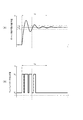
ここで、図5は、フィードバック制御が正常に実施された場合のギャップ検出器151及びコンパレーター156の出力値の一例を示すグラフである。図5(A)は、ギャップ検出器151の検出値を、図5(B)は、コンパレーターの出力値を示すグラフである。
図5(A)に示すように、波長可変干渉フィルター5の駆動が開始し、フィードバック制御が実施されると、ギャップ検出器151の検出値が振動する。そして、フィードバック制御が正常に実施される場合では、所定の安定化時間以内に検出値の振動が収まり安定化する。通常は、検出値は、振動を開始してから2周期程度で許容範囲に収まり、安定化する。
Here, FIG. 5 is a graph illustrating an example of output values of the
As shown in FIG. 5A, when the drive of the variable
安定化状態では、ギャップ検出器151の検出値の絶対値であるVabsが閾値電圧Vth以下である状態が継続する。すなわち、ギャップ検出器151の検出値が、図5(A)の一点鎖線で示す許容範囲L内に収まる。
なお、許容範囲Lは、図5の細い実線で示す目標値を中心とする所定電圧範囲であり、波長可変干渉フィルター5の仕様や測定精度等に応じて設定され、例えば、上記目標値を中心とする±10mVの範囲である。
In the stabilized state, the state in which V abs that is the absolute value of the detection value of the
The allowable range L is a predetermined voltage range centered on the target value indicated by the thin solid line in FIG. 5 and is set according to the specification, measurement accuracy, etc. of the wavelength
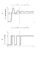
状態検出手段164により所定時間T0が経過するまで安定化したと判定されず(ステップS3;No、かつ、ステップS4;Yes)、つまり、安定化すべき時間までにギャップG1の変動が安定化していない(変動が収束していない)場合、状態検出手段164は、クローズドループシステムにおいて、フィードバックエラーが発生していることを検出する。この場合、状態検出手段164は、定常偏差型のフィードバックエラーを検出したか否かを判定する(ステップS5)。具体的には、状態検出手段164は、判定時間T1の間に、コンパレーター156から出力される電圧信号が、HighレベルVHのみであるか否かを判定する。
It is not determined that the state detection unit 164 has stabilized until the predetermined time T 0 has elapsed (step S3; No, and step S4; Yes), that is, the fluctuation of the gap G1 has been stabilized by the time to be stabilized. When there is no change (the fluctuation has not converged), the state detection unit 164 detects that a feedback error has occurred in the closed loop system. In this case, the state detection unit 164 determines whether or not a steady deviation type feedback error has been detected (step S5). Specifically, the state detection unit 164 determines whether or not the voltage signal output from the
ステップS5において、「Yes」と判定された場合、定常偏差型のフィードバックエラーが発生していると判定する。
図6は、定常偏差型のフィードバックエラーが発生している場合における検出値及びコンパレーターの出力値の特性の一例を示すグラフである。
図6に示すように、定常偏差型のフィードバックエラーでは、所定時間T0が経過した後、検出値が許容範囲を超えて収束する。なお、図6では、検出値が上限値を上回って収束する例を示し、検出値が下限値を下回って収束する場合の図示は省略している。
If it is determined as “Yes” in step S5, it is determined that a stationary deviation type feedback error has occurred.
FIG. 6 is a graph showing an example of the characteristics of the detected value and the output value of the comparator when a steady deviation type feedback error has occurred.
As shown in FIG. 6, in the case of a steady deviation type feedback error, after a predetermined time T 0 has elapsed, the detected value converges beyond the allowable range. FIG. 6 shows an example in which the detection value converges above the upper limit value, and illustration of the case where the detection value converges below the lower limit value is omitted.
定常偏差型のフィードバックエラーでは、図6(B)に示すように、所定時間T0の経過後から所定の判定時間T1が経過するまでの間、コンパレーター156からの電圧信号としてLowレベルVLの信号が出力される。従って、状態検出手段164は、判定時間T1内に継続してHighレベルVHを検出したか否かを検出することで、定常偏差型のフィードバックエラーであるか否かを判定できる。
In the stationary deviation type feedback error, as shown in FIG. 6B, the low level V is outputted as the voltage signal from the
この場合、バイアス指令手段162は、バイアス駆動部153におけるバイアス電圧を再設定する(ステップS6)。
具体的には、バイアス指令手段162は、減算回路154からマイコン16に入力される検出値と目標値との偏差が正値である場合、図6(A)に示すように、検出値である静電容量値が許容範囲の上限値を超えた値で収束している定常偏差型のフィードバック制御エラーが発生していると判定する。この場合、バイアス指令手段162は静電容量値を減少させるようにバイアス電圧値を減少させる。
逆に、バイアス指令手段162は、減算回路154から入力される検出値と目標値との偏差が負値である場合、検出値が許容範囲の下限値未満での値で収束していると判定し静電容量値を増大させるようにバイアス電圧を増大させる。
In this case, the
Specifically, when the deviation between the detection value input from the
Conversely, when the deviation between the detection value input from the
一方、ステップS5において、「No」と判定された場合、即ち、判定時間T1内において、HighレベルVH及びLowレベルVLの電圧信号が交互に出力されるような場合、状態検出手段164は、振動型のフィードバックエラー(発振エラー)と判定する。
図7は、振動型のフィードバックエラーが発生している場合における検出値及びコンパレーターの出力値の特性の一例を示すグラフである。
図7(B)に示すように、発振エラーでは、所定時間T0の経過後から所定の判定時間T1が経過するまでの間に、コンパレーター156からHighレベルVH及びLowレベルVLの信号が複数回出力される。従って、状態検出手段164は、判定時間T1内に、これらの交互に出力されたHighレベルVH及びLowレベルVLの電圧信号を検出することで、発振エラーを検出できる。
On the other hand, when it is determined as “No” in step S5, that is, when the voltage signals of the high level V H and the low level V L are alternately output within the determination time T 1 , the state detection unit 164 Is determined as a vibration type feedback error (oscillation error).
FIG. 7 is a graph showing an example of the characteristics of the detected value and the output value of the comparator when a vibration type feedback error has occurred.
As shown in FIG. 7B, in the oscillation error, the
この場合、ゲイン調整手段165は、フィードバック駆動部152のゲインを設定し、フィードバック電圧を制御する(ステップS7)。
ここで、図7(A)に示すように、検出値である静電容量値が収束しない、振動型のフィードバック制御エラーが発生している場合、フィードバック駆動部152のフィードバック制御のゲインが大きいことが考えられる。従って、ゲイン調整手段165はフィードバック駆動部152のフィードバック制御のゲインを減少させる。
なお、フィードバック駆動部152が、高精度のフィードバック制御が可能なPID(Proportional Integral Derivative)制御を採用している場合、例えば、比例動作(P動作)に関するゲイン(比例ゲイン)が大きいことが考えられる。従って、ゲイン調整手段165はフィードバック駆動部152のフィードバック制御の比例ゲインを減少させる。
In this case, the
Here, as illustrated in FIG. 7A, when a vibration type feedback control error has occurred in which the detected capacitance value does not converge, the feedback control gain of the
In addition, when the
なお、所定の判定時間T1は、例えば、検出値の振動周期(波長可変干渉フィルター5における保持部522のバネ性等により決定される固有周期)の1周期以上の所定の長さの時間である。判定時間T1を振動周期の1周期以上とすることで、振動(発振)している場合でも、収束している場合でも、エラーを検出することができる。
Note that the predetermined determination time T 1 is, for example, a time having a predetermined length that is one cycle or more of the oscillation cycle of the detection value (the natural cycle determined by the spring property of the holding
また、ゲイン調整手段165は、メモリー161に記憶されているデータやプログラム等を用いて目標信号を出力する。例えば、目標波長とフィードバック電圧(又は、フィードバック駆動部152のゲインの値)とを対応付けたデータや、目標波長に対応したフィードバック電圧を算出するためのプログラム等をメモリー161に記憶している。ゲイン調整手段165は、当該データやプログラム等を用いてフィードバック電圧(又は、フィードバック駆動部152のゲインの値)を算出する。目標指令手段163は、算出結果に応じた、目標信号をフィードバック駆動部152に出力する。
The
上述のステップS3〜S7を、ステップS3において安定化したと判定されるまで繰り返す。
なお、上記図6に示す定常偏差型のエラーと、図7に示す振動型のエラーが同時に発生している場合でも、上述のステップS3〜S7を繰りかえすことにより、安定化させることができる。例えば、検出値が、許容範囲Lの上限値を超えた範囲、又は下限値未満の範囲で発信している場合、ステップS5において、コンパレーター156の電圧信号の変動が検出されない(ステップS5;No)。従って、最初に、バイアス駆動部のゲインが調整される。その後、コンパレーター156の電圧信号の変動(すなわち、振動型のエラー)が検出され、フィードバック駆動部152のゲインが調整されることになる。
The above steps S3 to S7 are repeated until it is determined in step S3 that the operation has been stabilized.
In addition, even when the stationary deviation type error shown in FIG. 6 and the vibration type error shown in FIG. 7 occur at the same time, it can be stabilized by repeating the above steps S3 to S7. For example, when the detection value is transmitted in a range exceeding the upper limit value of the allowable range L or in a range less than the lower limit value, in step S5, the fluctuation of the voltage signal of the
波長可変干渉フィルター5のギャップG1の寸法が、ステップS1にて設定された目標波長に対応した寸法となると、ステップS3で安定化したと判定される。そして、波長可変干渉フィルター5から目標波長を中心とした光が出射される。ディテクター11に目標波長の光が受光され、制御部20の光量取得部22は、ディテクター11から入力された光量検出信号に基づいて、目標波長の光の光量を取得する(ステップS8)。
When the dimension of the gap G1 of the wavelength
[実施形態の作用効果]
電圧制御部15は、各静電アクチュエーター56A,56Bの駆動量の目標値(設定値)に応じて駆動電圧(バイアス電圧及びフィードバック電圧)を印加する。駆動開始から所定時間T0経過後における、ギャップ検出器151の検出値と設定値との差が許容範囲Lを越える場合、コンパレーター156の出力がHighレベルVHとなる場合がある。状態検出手段164は、コンパレーター156の出力がHighレベルVHとなったことを検出する。すなわち、各静電アクチュエーター56A,56Bの駆動が安定化するべきタイミングにおいて、駆動量の検出値と設定値との偏差の絶対値が許容範囲L内であるか否かを検出する。
これにより、フィードバック制御が適切に実施されておらず、ギャップG1の寸法(駆動量)の設定値に対して、実際のギャップG1の寸法(駆動量)が、所定の閾値を超えた値で安定していたり、振動し続けていたりすることを検出でき、フィードバック制御のエラーを検出することができる。
[Effects of Embodiment]
The
As a result, the feedback control is not properly performed, and the actual size (drive amount) of the gap G1 is stable at a value exceeding a predetermined threshold with respect to the set value of the size (drive amount) of the gap G1. It can be detected that the motor is oscillating or continues to vibrate, and an error in feedback control can be detected.
ここで、フィードバック制御において、安定化時間内でアクチュエーターを安定化させるためには、フィードバック駆動部152やバイアス駆動部153により印加される電圧値(駆動パラメーター)の値が適性値であることが望ましい。例えば、フィードバック駆動部152のゲイン(駆動パラメーター)の値が適性値に対して大きいと、アクチュエーターの駆動量の変動が収束しない(すなわち、発振する)、又は収束するまでの時間が著しく長くなることがある。
これに対して、電圧制御部15は、所定時間T0経過後に、ギャップ検出器151の検出値と設定値との偏差の絶対値として、閾値を超える偏差の絶対値、及び閾値未満の偏差の絶対値を交互に複数回検出することで、各静電アクチュエーター56A,56Bが発振していることを検出する。すなわち、安定化時間が経過しても、駆動量の変動が収束しておらず、フィードバック制御のエラーとして、振動型のエラーを検出できる。これにより、フィードバック駆動部152のゲインを調整することができ、駆動量を収束させることができる。
Here, in the feedback control, in order to stabilize the actuator within the stabilization time, it is desirable that the value of the voltage value (drive parameter) applied by the
On the other hand, after the predetermined time T 0 has elapsed, the
本実施形態では、アクチュエーターが、第一静電アクチュエーター56A及び第二静電アクチュエーター56Bにより構成され、第一静電アクチュエーター56Aにはバイアス電圧が印加され、第二静電アクチュエーター56Bにはフィードバック電圧が印加される。このようなアクチュエーターでは、バイアス電圧の印加により第一静電アクチュエーター56Aを粗動駆動させる。一方、ギャップ検出器151の検出値(駆動量)に基づいてフィードバック電圧を制御し、第二静電アクチュエーター56Bを微動駆動させることで、アクチュエーターの駆動量を精度よく制御することができる。
In the present embodiment, the actuator includes a first
ここで、バイアス電圧が適性値よりも大きい又は小さい場合、第一静電アクチュエーター56Aの粗動駆動による駆動量と設定値との偏差の絶対値が、第二静電アクチュエーター56Bの微動駆動による調整範囲で対応可能な範囲の閾値を超える場合がある。すなわち、バイアス電圧が大きすぎたり、小さすぎたりすると、フィードバック電圧の最小値又は最大値で駆動量の変動が収束したとしても、ギャップ検出器151の検出値を許容範囲L上限よりも大きい値や、下限よりも小さい値で安定してしまう場合がある。
これに対して、検出値が許容範囲Lの範囲外で収束している場合、すなわち定常偏差型のエラー(図6参照)が発生し、粗動駆動による駆動量と設定値との差が、微動駆動の調整可能な範囲を超えている状態であることを検出できる。そして、検出結果に応じて、バイアス指令手段162がバイアス電圧(駆動パラメーター)を調整する。これにより、粗動駆動の駆動量を微動駆動の調整可能な範囲に収めることができ、アクチュエーターの駆動量をより確実、かつ精度よく制御することができる。
Here, when the bias voltage is larger or smaller than the appropriate value, the absolute value of the deviation between the driving amount by the coarse driving of the first
On the other hand, when the detected value has converged outside the allowable range L, that is, a steady deviation error (see FIG. 6) occurs, and the difference between the drive amount due to the coarse drive and the set value is It can be detected that the fine movement drive is beyond the adjustable range. Then, the bias command means 162 adjusts the bias voltage (drive parameter) according to the detection result. As a result, the driving amount of the coarse driving can be within the adjustable range of the fine driving, and the driving amount of the actuator can be controlled more reliably and accurately.
また、状態検出手段164は、駆動開始から所定時間T0経過後に、ギャップ検出器151の検出値と設定値との偏差の絶対値として、閾値を超える偏差の絶対値、及び閾値未満の偏差の絶対値を交互に複数回検出した際に、フィードバック駆動部152のゲインを小さくして、フィードバック電圧を制御する。すなわち、第二静電アクチュエーター56Bにおける、フィードバック制御のゲインが大きいため、安定化時間に到達しても、ギャップ検出器151の検出値が収束しておらず振動していること、振動型のエラー(図7参照)を検出する。そして、検出結果に基づいて、フィードバック駆動部152によるフィードバック制御のゲインを小さくしてフィードバック電圧を制御することにより、駆動量を収束させることができ、アクチュエーターの駆動量をより確実、かつ精度よく制御することができる。
In addition, the state detection unit 164 receives the absolute value of the deviation exceeding the threshold and the deviation less than the threshold as the absolute value of the deviation between the detection value of the
状態検出手段164は、上述の安定化時間以上に設定された所定時間T0が経過した後にエラー検出を実施する。これにより、安定化する前に状態検出手段164によるエラー検出が実施されることで、誤ってエラーが検出されることを抑制できる。
なお、所定時間T0の長さは、安定化時間以上であることが好ましく、安定化時間以上であれば特に制限されないが、安定化時間に対して所定時間T0が長くなりすぎると、エラーの検出タイミングまでの待機時間が長くなるため、測定時間が長くなるおそれがある。適正なフィードバック制御が実施されている場合に確実に安定化させることができる長さに安定化時間が設定されている場合は、安定化時間を所定時間T0に設定することで、測定時間を短縮できる。
The state detection unit 164 performs error detection after a predetermined time T 0 set longer than the stabilization time described above has elapsed. Thereby, it can suppress that an error is detected accidentally by performing the error detection by the state detection means 164 before stabilizing.
The length of the predetermined time T 0 is preferably equal to or longer than the stabilization time, and is not particularly limited as long as it is equal to or longer than the stabilization time. However, if the predetermined time T 0 becomes too long with respect to the stabilization time, an error occurs. Since the waiting time until the detection timing becomes longer, the measurement time may be longer. If the stabilization time is set to a length that can be reliably stabilized when appropriate feedback control is performed, the measurement time can be set by setting the stabilization time to the predetermined time T 0. Can be shortened.
分光測定装置1では、駆動開始から所定時間T0の経過前に状態検出手段164によってギャップG1の寸法が安定化したことが検出されると、予め設定されている所定時間T0の経過前であっても、分光測定を実施する。これにより、安定化しているにも関わらず測定が開始されないで分光測定装置1が待機している時間が生じることを抑制でき、測定時間を短縮できる。
In the
[その他の実施形態]
なお、本発明は前述の実施形態に限定されるものではなく、本発明の目的を達成できる範囲での変形、改良等は本発明に含まれるものである。
例えば、本発明において、アクチュエーターとして、波長可変干渉フィルター5におけるギャップG1の寸法を変化させる静電アクチュエーターを例示したが、これに限定されない。アクチュエーターとしては、例えば、圧電アクチュエーターや、誘電コイルアクチュエーター等、他のアクチュエーターを用いたフィードバックループを対象としてもよい。特に、駆動電圧に対して駆動量が非線形に変動するアクチュエーターの場合、駆動特性の変動により、フィードバック制御時に最適なゲインが設定されていないと、上述したように、異常発振等、正常な駆動が妨げられるおそれがある。本発明は、このような駆動特性が非線形に変動するアクチュエーターに有効であり、最適なゲインを設定することで、最適な制御状態を維持したフィードバック制御を実施することができる。
[Other Embodiments]
It should be noted that the present invention is not limited to the above-described embodiments, and modifications, improvements, and the like within the scope that can achieve the object of the present invention are included in the present invention.
For example, in the present invention, an electrostatic actuator that changes the dimension of the gap G1 in the wavelength
上記実施形態では、反射膜54,55を容量検出量の電極として利用したが、これに限定されない。例えば、反射膜54,55とは別に固定基板51及び可動基板52に、互いに対向する容量検出用電極を設けてもよい。
In the above embodiment, the
また、駆動量の検出手段として、上述のような静電容量検出電極を用いる構成に限られず、例えば、歪ゲージ等により、可動基板52(保持部522)の湾曲状態を検出して、反射膜間ギャップG1のギャップ量を検出する構成としてもよく、外部にギャップ量を検出するための光センサーを設ける構成などとしてもよい。 The drive amount detection means is not limited to the configuration using the capacitance detection electrode as described above. For example, the curved state of the movable substrate 52 (holding portion 522) is detected by a strain gauge or the like, and the reflection film is detected. The gap amount of the inter-gap G1 may be detected, or an optical sensor for detecting the gap amount may be provided outside.
上記実施形態において、バイアス電圧が印加される第一静電アクチュエーター56Aは、フィードバック電圧が印加される第二静電アクチュエーター56Bの外周側に配置される例を示したが、これに限定されない。例えば、第一静電アクチュエーター56Aが、反射膜54,55の外周側で、第二静電アクチュエーター56Bの内周側に設けられ、第二静電アクチュエーター56Bが第一静電アクチュエーター56Aの外周側に設けられる構成などとしてもよい。
In the embodiment described above, the first
上記実施形態では、複数のアクチュエーターとして、第一静電アクチュエーター56A及び第二静電アクチュエーター56Bを備え、第一静電アクチュエーター56Aにバイアス電圧を、第二静電アクチュエーター56Bにフィードバック電圧を印加する構成を例示したが、本発明はこれに限定されず、1つのアクチュエーターを備える構成としてもよい。この場合、例えば、1つのバイアス電圧が印加される第一静電アクチュエーター56Aに相当するアクチュエーターを設けずに、第二静電アクチュエーター56Bに相当する1つのアクチュエーターのみを設け、駆動量の検出値に応じてフィードバック制御のゲインを調整するように構成する。
In the above embodiment, the first
上記実施形態では、減算回路154を設け、151の検出値と設定値との偏差を取得する構成を例示したが、本発明はこれに限定されず、減算回路154を設けなくてもよい。例えば、152においてフィードバック制御を実施する際に、取得した上記偏差を用いる構成が例示できる。
In the above embodiment, the configuration in which the
上記実施形態では、減算回路154、絶対値回路155、及びコンパレーター156であるアナログ回路を備える構成を例示したが、本発明はこれに限定されない。例えば、上記アナログ回路を備えず、151の検出値と設定値との偏差を取得し、当該偏差に基づく安定化の検出や、エラーの検出をマイコン16により実施する構成としてもよい。
In the above embodiment, the configuration including the analog circuit that is the
また、本発明の電子機器として、上記実施形態では、分光測定装置1を例示したが、その他、様々な分野により本発明の波長可変干渉フィルターの駆動方法、光学モジュール、及び電子機器を適用することができる。
In the above embodiment, the
例えば、図8に示すように、本発明の電子機器を、色を測定するための測色装置に適用することもできる。
図8は、波長可変干渉フィルターを備えた測色装置400の一例を示すブロック図である。
この測色装置400は、図8に示すように、検査対象Aに光を射出する光源装置410と、測色センサー420(光学モジュール)と、測色装置400の全体動作を制御する制御装置430(処理部)とを備える。そして、この測色装置400は、光源装置410から射出される光を検査対象Aにて反射させ、反射された検査対象光を測色センサー420にて受光し、測色センサー420から出力される検出信号に基づいて、検査対象光の色度、すなわち検査対象Aの色を分析して測定する装置である。
For example, as shown in FIG. 8, the electronic apparatus of the present invention can also be applied to a color measuring device for measuring color.
FIG. 8 is a block diagram illustrating an example of a
As shown in FIG. 8, the
光源装置410、光源411、複数のレンズ412(図8には1つのみ記載)を備え、検査対象Aに対して例えば基準光(例えば、白色光)を射出する。また、複数のレンズ412には、コリメーターレンズが含まれてもよく、この場合、光源装置410は、光源411から射出された基準光をコリメーターレンズにより平行光とし、図示しない投射レンズから検査対象Aに向かって射出する。なお、本実施形態では、光源装置410を備える測色装置400を例示するが、例えば検査対象Aが液晶パネルなどの発光部材である場合、光源装置410が設けられない構成としてもよい。
A
測色センサー420は、図8に示すように、波長可変干渉フィルター5と、波長可変干渉フィルター5を透過する光を受光するディテクター11と、波長可変干渉フィルター5で透過させる光の波長を可変する電圧制御部15とを備える。また、測色センサー420は、波長可変干渉フィルター5に対向する位置に、検査対象Aで反射された反射光(検査対象光)を、内部に導光する図示しない入射光学レンズを備えている。そして、この測色センサー420は、波長可変干渉フィルター5により、入射光学レンズから入射した検査対象光のうち、所定波長の光を分光し、分光した光をディテクター11にて受光する。
As shown in FIG. 8, the
制御装置430は、測色装置400の全体動作を制御する。
この制御装置430としては、例えば汎用パーソナルコンピューターや、携帯情報端末、その他、測色専用コンピューターなどを用いることができる。そして、制御装置430は、図8に示すように、光源制御部431、測色センサー制御部432、及び測色処理部433などを備えて構成されている。
光源制御部431は、光源装置410に接続され、例えば利用者の設定入力に基づいて、光源装置410に所定の制御信号を出力して、所定の明るさの白色光を射出させる。
測色センサー制御部432は、測色センサー420に接続され、例えば利用者の設定入力に基づいて、測色センサー420にて受光させる光の波長を設定し、この波長の光の受光量を検出する旨の制御信号を測色センサー420に出力する。これにより、測色センサー420の電圧制御部15は、制御信号に基づいて、静電アクチュエーター56に電圧を印加し、波長可変干渉フィルター5を駆動させる。
測色処理部433は、ディテクター11により検出された受光量から、検査対象Aの色度を分析する。
The
As the
The light
The colorimetric
The
また、本発明の電子機器の他の例として、特定物質の存在を検出するための光ベースのシステムが挙げられる。このようなシステムとしては、例えば、本発明の波長可変干渉フィルターを用いた分光計測方式を採用して特定ガスを高感度検出する車載用ガス漏れ検出器や、呼気検査用の光音響希ガス検出器等のガス検出装置を例示できる。
このようなガス検出装置の一例を以下に図面に基づいて説明する。
Another example of the electronic device of the present invention is a light-based system for detecting the presence of a specific substance. As such a system, for example, an in-vehicle gas leak detector that detects a specific gas with high sensitivity by adopting a spectroscopic measurement method using the variable wavelength interference filter of the present invention, or a photoacoustic rare gas detection for a breath test. A gas detection device such as a vessel can be exemplified.
An example of such a gas detection device will be described below with reference to the drawings.
図9は、波長可変干渉フィルターを備えたガス検出装置の一例を示す概略図である。
図10は、図9のガス検出装置の制御系の構成を示すブロック図である。
このガス検出装置100は、図9に示すように、センサーチップ110と、吸引口120A、吸引流路120B、排出流路120C、及び排出口120Dを備えた流路120と、本体部130と、を備えて構成されている。
本体部130は、流路120を着脱可能な開口を有するセンサー部カバー131、排出手段133、筐体134、光学部135、フィルター136、波長可変干渉フィルター5、及び受光素子137(検出部)等を含む検出装置(光学モジュール)と、検出された信号を処理し、検出部を制御する制御部138(処理部)、電力を供給する電力供給部139等から構成されている。また、光学部135は、光を射出する光源135Aと、光源135Aから入射された光をセンサーチップ110側に反射し、センサーチップ側から入射された光を受光素子137側に透過するビームスプリッター135Bと、レンズ135C,135D,135Eと、により構成されている。
また、図10に示すように、ガス検出装置100の表面には、操作パネル140、表示部141、外部とのインターフェイスのための接続部142、電力供給部139が設けられている。電力供給部139が二次電池の場合には、充電のための接続部143を備えてもよい。
更に、ガス検出装置100の制御部138は、図10に示すように、CPU等により構成された信号処理部144、光源135Aを制御するための光源ドライバー回路145、波長可変干渉フィルター5を制御するための電圧制御部146、受光素子137からの信号を受信する受光回路147、センサーチップ110のコードを読み取り、センサーチップ110の有無を検出するセンサーチップ検出器148からの信号を受信するセンサーチップ検出回路149、及び排出手段133を制御する排出ドライバー回路150などを備えている。
FIG. 9 is a schematic diagram illustrating an example of a gas detection apparatus including a wavelength variable interference filter.
FIG. 10 is a block diagram showing a configuration of a control system of the gas detection device of FIG.
As illustrated in FIG. 9, the
The
As shown in FIG. 10, an
Furthermore, as shown in FIG. 10, the
次に、上記のようなガス検出装置100の動作について、以下に説明する。
本体部130の上部のセンサー部カバー131の内部には、センサーチップ検出器148が設けられており、このセンサーチップ検出器148でセンサーチップ110の有無が検出される。信号処理部144は、センサーチップ検出器148からの検出信号を検出すると、センサーチップ110が装着された状態であると判断し、表示部141へ検出動作を実施可能な旨を表示させる表示信号を出す。
Next, operation | movement of the above
A
そして、例えば利用者により操作パネル140が操作され、操作パネル140から検出処理を開始する旨の指示信号が信号処理部144へ出力されると、まず、信号処理部144は、光源ドライバー回路145に光源作動の信号を出力して光源135Aを作動させる。光源135Aが駆動されると、光源135Aから単一波長で直線偏光の安定したレーザー光が射出される。また、光源135Aには、温度センサーや光量センサーが内蔵されており、その情報が信号処理部144へ出力される。そして、信号処理部144は、光源135Aから入力された温度や光量に基づいて、光源135Aが安定動作していると判断すると、排出ドライバー回路150を制御して排出手段133を作動させる。これにより、検出すべき標的物質(ガス分子)を含んだ気体試料が、吸引口120Aから、吸引流路120B、センサーチップ110内、排出流路120C、排出口120Dへと誘導される。なお、吸引口120Aには、除塵フィルター120A1が設けられ、比較的大きい粉塵や一部の水蒸気などが除去される。
For example, when the
また、センサーチップ110は、金属ナノ構造体が複数組み込まれ、局在表面プラズモン共鳴を利用したセンサーである。このようなセンサーチップ110では、レーザー光により金属ナノ構造体間で増強電場が形成され、この増強電場内にガス分子が入り込むと、分子振動の情報を含んだラマン散乱光、及びレイリー散乱光が発生する。
これらのレイリー散乱光やラマン散乱光は、光学部135を通ってフィルター136に入射し、フィルター136によりレイリー散乱光が分離され、ラマン散乱光が波長可変干渉フィルター5に入射する。そして、信号処理部144は、電圧制御部146に対して制御信号を出力する。これにより、電圧制御部146は、上記実施形態に示すように、ギャップ検出器151、フィードバック駆動部152、及びマイコン16により構成され、上記実施形態と同様の駆動方法により、波長可変干渉フィルター5を駆動させ、検出対象となるガス分子に対応したラマン散乱光を波長可変干渉フィルター5で分光させる。
この後、分光した光が受光素子137で受光されると、受光量に応じた受光信号が受光回路147を介して信号処理部144に出力される。この場合、波長可変干渉フィルター5から目的とするラマン散乱光を精度よく取り出すことができる。
信号処理部144は、上記のようにして得られた検出対象となるガス分子に対応したラマン散乱光のスペクトルデータと、ROMに格納されているデータとを比較し、目的のガス分子か否かを判定し、物質の特定をする。また、信号処理部144は、表示部141にその結果情報を表示させたり、接続部142から外部へ出力したりする。
The
These Rayleigh scattered light and Raman scattered light enter the
Thereafter, when the dispersed light is received by the
The
なお、上記図9及び図10において、ラマン散乱光を波長可変干渉フィルター5により分光して分光されたラマン散乱光からガス検出を行うガス検出装置100を例示したが、ガス検出装置として、ガス固有の吸光度を検出することでガス種別を特定するガス検出装置として用いてもよい。この場合、センサー内部にガスを流入させ、入射光のうちガスにて吸収された光を検出するガスセンサーを本発明の光学モジュールとして用いる。そして、このようなガスセンサーによりセンサー内に流入されたガスを分析、判別するガス検出装置を本発明の電子機器とする。このような構成でも、波長可変干渉フィルターを用いてガスの成分を検出することができる。
9 and 10 exemplify the
また、特定物質の存在を検出するためのシステムとして、上記のようなガスの検出に限られず、近赤外線分光による糖類の非侵襲的測定装置や、食物や生体、鉱物等の情報の非侵襲的測定装置等の、物質成分分析装置を例示できる。
以下に、上記物質成分分析装置の一例として、食物分析装置を説明する。
In addition, the system for detecting the presence of a specific substance is not limited to the detection of the gas as described above, but a non-invasive measuring device for saccharides by near-infrared spectroscopy, and non-invasive information on food, living body, minerals, etc. A substance component analyzer such as a measuring device can be exemplified.
Hereinafter, a food analyzer will be described as an example of the substance component analyzer.
図11は、波長可変干渉フィルター5を利用した電子機器の一例である食物分析装置の概略構成を示す図である。
この食物分析装置200は、図11に示すように、検出器210(光学モジュール)と、制御部220と、表示部230と、を備えている。検出器210は、光を射出する光源211と、測定対象物からの光が導入される撮像レンズ212と、撮像レンズ212から導入された光を分光する波長可変干渉フィルター5と、分光された光を検出する撮像部213(検出部)と、を備えている。
また、制御部220は、光源211の点灯・消灯制御、点灯時の明るさ制御を実施する光源制御部221と、波長可変干渉フィルター5を制御する電圧制御部222と、撮像部213を制御し、撮像部213で撮像された分光画像を取得する検出制御部223と、信号処理部224(分析部)と、記憶部225と、を備えている。
FIG. 11 is a diagram illustrating a schematic configuration of a food analyzer that is an example of an electronic apparatus using the wavelength
As shown in FIG. 11, the
In addition, the
この食物分析装置200は、システムを駆動させると、光源制御部221により光源211が制御されて、光源211から測定対象物に光が照射される。そして、測定対象物で反射された光は、撮像レンズ212を通って波長可変干渉フィルター5に入射する。波長可変干渉フィルター5は電圧制御部222の制御により上記実施形態に示すような駆動方法で駆動される。これにより、波長可変干渉フィルター5から精度よく目的波長の光を取り出すことができる。そして、取り出された光は、例えばCCDカメラ等により構成される撮像部213で撮像される。また、撮像された光は分光画像として、記憶部225に蓄積される。また、信号処理部224は、電圧制御部222を制御して波長可変干渉フィルター5に印加する電圧値を変化させ、各波長に対する分光画像を取得する。
In the
そして、信号処理部224は、記憶部225に蓄積された各画像における各画素のデータを演算処理し、各画素におけるスペクトルを求める。また、記憶部225には、例えばスペクトルに対する食物の成分に関する情報が記憶されており、信号処理部224は、求めたスペクトルのデータを、記憶部225に記憶された食物に関する情報を基に分析し、検出対象に含まれる食物成分、及びその含有量を求める。また、得られた食物成分及び含有量から、食物カロリーや鮮度等をも算出することができる。更に、画像内のスペクトル分布を分析することで、検査対象の食物の中で鮮度が低下している部分の抽出等をも実施することができ、更には、食物内に含まれる異物等の検出をも実施することができる。
そして、信号処理部224は、上述のようにして得られた検査対象の食物の成分や含有量、カロリーや鮮度等の情報を表示部230に表示させる処理をする。
Then, the
Then, the
また、図11において、食物分析装置200の例を示すが、略同様の構成により、上述したようなその他の情報の非侵襲的測定装置としても利用することができる。例えば、血液等の体液成分の測定、分析等、生体成分を分析する生体分析装置として用いることができる。このような生体分析装置としては、例えば血液等の体液成分を測定する装置として、エチルアルコールを検知する装置とすれば、運転者の飲酒状態を検出する酒気帯び運転防止装置として用いることができる。また、このような生体分析装置を備えた電子内視鏡システムとしても用いることができる。
更には、鉱物の成分分析を実施する鉱物分析装置としても用いることができる。
Moreover, although the example of the
Furthermore, it can also be used as a mineral analyzer for performing component analysis of minerals.
更には、本発明の波長可変干渉フィルター、光学モジュール、電子機器としては、以下のような装置に適用することができる。
例えば、各波長の光の強度を経時的に変化させることで、各波長の光でデータを伝送させることも可能であり、この場合、光学モジュールに設けられた波長可変干渉フィルターにより特定波長の光を分光し、受光部で受光させることで、特定波長の光により伝送されるデータを抽出することができ、このようなデータ抽出用光学モジュールを備えた電子機器により、各波長の光のデータを処理することで、光通信を実施することもできる。
Furthermore, the variable wavelength interference filter, optical module, and electronic apparatus of the present invention can be applied to the following devices.
For example, it is possible to transmit data using light of each wavelength by changing the intensity of light of each wavelength over time. In this case, light of a specific wavelength is transmitted by a wavelength variable interference filter provided in the optical module. The data transmitted by the light of the specific wavelength can be extracted by separating the light and receiving the light at the light receiving unit, and the electronic data having such a data extraction optical module can be used to extract the light data of each wavelength. By processing, optical communication can be performed.
また、電子機器としては、本発明の波長可変干渉フィルターにより光を分光することで、分光画像を撮像する分光カメラ、分光分析機などにも適用できる。このような分光カメラの一例として、波長可変干渉フィルターを内蔵した赤外線カメラが挙げられる。
図12は、分光カメラの概略構成を示す模式図である。分光カメラ300は、図12に示すように、カメラ本体310と、撮像レンズユニット320と、撮像部330(検出部)とを備えている。
カメラ本体310は、利用者により把持、操作される部分である。
撮像レンズユニット320は、カメラ本体310に設けられ、入射した画像光を撮像部330に導光する。また、この撮像レンズユニット320は、図12に示すように、対物レンズ321、結像レンズ322、及びこれらのレンズ間に設けられた波長可変干渉フィルター5を備えて構成されている。
撮像部330は、受光素子により構成され、撮像レンズユニット320により導光された画像光を撮像する。
このような分光カメラ300では、波長可変干渉フィルター5により撮像対象となる波長の光を透過させることで、所望波長の光の分光画像を撮像することができる。この時、各波長に対して、電圧制御部(図示略)が上記実施形態に示すような本発明の駆動方法により波長可変干渉フィルター5を駆動させることで、精度よく目的波長の分光画像の画像光を取り出すことができる。
Further, the electronic apparatus can be applied to a spectroscopic camera, a spectroscopic analyzer, or the like that captures a spectroscopic image by dispersing light with the variable wavelength interference filter of the present invention. An example of such a spectroscopic camera is an infrared camera incorporating a wavelength variable interference filter.
FIG. 12 is a schematic diagram showing a schematic configuration of the spectroscopic camera. As shown in FIG. 12, the
The
The
The
In such a
更には、本発明の波長可変干渉フィルターをバンドパスフィルターとして用いてもよく、例えば、発光素子が射出する所定波長域の光のうち、所定の波長を中心とした狭帯域の光のみを波長可変干渉フィルターで分光して透過させる光学式レーザー装置としても用いることができる。
また、本発明の波長可変干渉フィルターを生体認証装置として用いてもよく、例えば、近赤外領域や可視領域の光を用いた、血管や指紋、網膜、虹彩などの認証装置にも適用できる。
Furthermore, the wavelength tunable interference filter of the present invention may be used as a bandpass filter. For example, only light in a narrow band centered on a predetermined wavelength is tunable out of light in a predetermined wavelength range emitted from a light emitting element. It can also be used as an optical laser device that spectrally transmits through an interference filter.
In addition, the tunable interference filter of the present invention may be used as a biometric authentication device, and can be applied to authentication devices such as blood vessels, fingerprints, retinas, and irises using light in the near infrared region and visible region.
更には、光学モジュール及び電子機器を、濃度検出装置として用いることができる。この場合、波長可変干渉フィルターにより、物質から射出された赤外エネルギー(赤外光)を分光して分析し、サンプル中の被検体濃度を測定する。 Furthermore, an optical module and an electronic device can be used as a concentration detection device. In this case, the infrared energy (infrared light) emitted from the substance is spectrally analyzed by the variable wavelength interference filter, and the analyte concentration in the sample is measured.
上記に示すように、本発明の波長可変干渉フィルター、光学モジュール、及び電子機器は、入射光から所定の光を分光するいかなる装置にも適用することができる。そして、本発明の波長可変干渉フィルターは、上述のように、1デバイスで複数の波長を分光させることができるため、複数の波長のスペクトルの測定、複数の成分に対する検出を精度よく実施することができる。従って、複数デバイスにより所望の波長を取り出す従来の装置に比べて、光学モジュールや電子機器の小型化を促進でき、例えば、携帯用や車載用の光学デバイスとして好適に用いることができる。 As described above, the tunable interference filter, the optical module, and the electronic device of the present invention can be applied to any device that splits predetermined light from incident light. Since the wavelength tunable interference filter according to the present invention can split a plurality of wavelengths with one device as described above, it is possible to accurately measure a spectrum of a plurality of wavelengths and detect a plurality of components. it can. Therefore, compared with the conventional apparatus which takes out a desired wavelength with a plurality of devices, it is possible to promote downsizing of the optical module and the electronic apparatus, and for example, it can be suitably used as a portable or in-vehicle optical device.
更に、上述した実施形態では、基板間に設けられた各静電アクチュエーター56A,56Bのギャップ寸法から駆動特性を取得し、各静電アクチュエーター56A,56Bのフィードバック制御におけるゲインを設定する例を示したが、これに限定されない。
例えば、電圧印加により、駆動電圧に対して駆動量が非線形に変化するアクチュエーター駆動装置のフィードバック制御に利用することができ、このようなアクチュエーターとして例えば、ピエゾアクチュエーター等が挙げられる。具体的には、ピエゾアクチュエーターに駆動電圧を印加することで、ミラーを駆動電圧に応じた角度だけ姿勢を変更させるミラーデバイス等にも適用できる。この場合、所定の駆動電圧を印加した際のピエゾアクチュエーターの駆動量(駆動角度等)を検出することで、ピエゾアクチュエーターの駆動特性を取得し、取得した駆動特性に基づいてピエゾアクチュエーターの駆動をフィードバック制御する構成等が挙げられる。
Furthermore, in the above-described embodiment, an example has been shown in which drive characteristics are acquired from the gap dimensions of the
For example, it can be used for feedback control of an actuator driving device whose driving amount changes nonlinearly with respect to the driving voltage by applying a voltage. Examples of such an actuator include a piezo actuator. Specifically, the present invention can also be applied to a mirror device that changes the attitude of the mirror by an angle corresponding to the driving voltage by applying a driving voltage to the piezo actuator. In this case, by detecting the drive amount (drive angle, etc.) of the piezo actuator when a predetermined drive voltage is applied, the drive characteristics of the piezo actuator are acquired, and the drive of the piezo actuator is fed back based on the acquired drive characteristics. The structure etc. to control are mentioned.
その他、本発明の実施の際の具体的な構造は、本発明の目的を達成できる範囲で他の構造等に適宜変更できる。 In addition, the specific structure for carrying out the present invention can be appropriately changed to other structures and the like within a range in which the object of the present invention can be achieved.
1…分光測定装置(電子機器)、10…光学モジュール、15…電圧制御部(フィードバックループ)、16…マイコン、20…制御部(処理部)、54…固定反射膜、55…可動反射膜、56…静電アクチュエーター、56A…第一静電アクチュエーター、56B…第二静電アクチュエーター、100…ガス検出装置(電子機器)、146…電圧制御部、151…ギャップ検出器(検出手段)、152…フィードバック駆動部(制御器)、153…バイアス駆動部(バイアス電圧印加手段)、154…減算回路(偏差検出手段)、155…絶対値回路(偏差検出手段)、156…コンパレーター(偏差検出手段)、162…バイアス指令手段(パラメーター補正手段)、163…目標指令手段、165…ゲイン調整手段(パラメーター補正手段)、200…食物分析装置、223…検出制御部(処理部)、300…分光カメラ(電子機器)、400…測色装置(電子機器)。
DESCRIPTION OF
Claims (6)
前記アクチュエーターの駆動量を検出する検出手段と、
前記検出手段により検出された前記駆動量の検出値、及び前記駆動量の設定値に応じて、前記アクチュエーターに印加する駆動電圧を制御するフィードバックループと、を具備し、
前記フィードバックループは、前記アクチュエーターの駆動開始から所定時間経過後における、前記検出値と前記設定値との偏差の絶対値が所定閾値を超えるか否かを検出する偏差検出手段を備えている
ことを特徴とするアクチュエーター制御装置。 An actuator that is driven by application of a driving voltage;
Detecting means for detecting the driving amount of the actuator;
A feedback loop that controls a drive voltage applied to the actuator according to a detection value of the drive amount detected by the detection means and a set value of the drive amount; and
The feedback loop includes deviation detecting means for detecting whether or not an absolute value of a deviation between the detected value and the set value exceeds a predetermined threshold after a predetermined time has elapsed from the start of driving of the actuator. Characteristic actuator control device.
前記偏差検出手段により前記偏差の絶対値が前記閾値を超えたと判定された場合に、前記フィードバックループにおける前記アクチュエーターの駆動パラメーターを補正するパラメーター補正手段を備えた
ことを特徴とするアクチュエーター制御装置。 The actuator control device according to claim 1,
An actuator control device, comprising: parameter correction means for correcting a drive parameter of the actuator in the feedback loop when the deviation detection means determines that the absolute value of the deviation exceeds the threshold value.
パラメーター補正手段は、前記偏差検出手段により前記所定時間経過後に、前記絶対値が前記閾値以下の前記偏差と、前記閾値を超える前記偏差とが交互に複数回検出された場合に、前記フィードバックループにおけるゲインを小さくする
ことを特徴とするアクチュエーター制御装置。 In the actuator control device according to claim 2,
The parameter correction means, in the feedback loop, when the deviation detecting means detects the deviation whose absolute value is equal to or less than the threshold and the deviation exceeding the threshold multiple times alternately after the predetermined time has elapsed. An actuator control device characterized in that gain is reduced.
前記アクチュエーターは、互いに独立して駆動可能な第一アクチュエーターと、第二アクチュエーターと、を備え、
前記フィードバックループは、前記第一アクチュエーターに対して所定のバイアス電圧を印加するバイアス電圧印加手段と、前記検出手段により検出された前記駆動量、及び前記アクチュエーターの駆動量の目標値に基づいて前記第二アクチュエーターに印加する駆動電圧を制御する制御器と、を備え、
前記パラメーター補正手段は、前記偏差検出手段により、前記所定時間経過後に、前記絶対値が前記閾値以上の前記偏差が継続して検出された場合に、前記バイアス電圧印加手段における前記バイアス電圧を変更する
ことを特徴とするアクチュエーター制御装置。 In the actuator control device according to claim 2 or 3,
The actuator includes a first actuator that can be driven independently of each other, and a second actuator,
The feedback loop includes a bias voltage applying unit that applies a predetermined bias voltage to the first actuator, the driving amount detected by the detecting unit, and a target value of the driving amount of the actuator. A controller for controlling the drive voltage applied to the two actuators,
The parameter correcting means changes the bias voltage in the bias voltage applying means when the deviation detecting means continuously detects the deviation whose absolute value is equal to or greater than the threshold after the predetermined time has elapsed. An actuator control device characterized by that.
駆動電圧の印加により駆動し、駆動量に応じて前記一対の反射膜間のギャップ寸法を変化させるアクチュエーターと、
前記アクチュエーターの駆動量を検出する検出手段と、
前記検出手段により検出された前記駆動量の検出値、及び前記駆動量の設定値に応じて、前記アクチュエーターに印加する駆動電圧を制御するフィードバックループと、を具備し、
前記フィードバックループは、前記アクチュエーターの駆動開始から所定時間経過後における、前記検出値と前記設定値との偏差の絶対値が所定閾値を超えるか否かを検出する偏差検出手段を備えている
ことを特徴とする光学モジュール。 A pair of reflective films facing each other;
An actuator that is driven by application of a driving voltage and changes a gap dimension between the pair of reflective films according to a driving amount;
Detecting means for detecting the driving amount of the actuator;
A feedback loop that controls a drive voltage applied to the actuator according to a detection value of the drive amount detected by the detection means and a set value of the drive amount; and
The feedback loop includes deviation detecting means for detecting whether or not an absolute value of a deviation between the detected value and the set value exceeds a predetermined threshold after a predetermined time has elapsed from the start of driving of the actuator. A featured optical module.
前記アクチュエーターの駆動量を検出する検出手段と、
前記検出手段により検出された前記駆動量の検出値、及び前記駆動量の設定値に応じて、前記アクチュエーターに印加する駆動電圧を制御するフィードバックループと、
前記アクチュエーターの駆動により所定の処理を実施する処理部と、を具備し、
前記フィードバックループは、前記アクチュエーターの駆動開始から所定時間経過後における、前記検出値と前記設定値との偏差の絶対値が所定閾値を超えるか否かを検出する偏差検出手段を備えている
ことを特徴とする電子機器。 An actuator that is driven by application of a driving voltage;
Detecting means for detecting the driving amount of the actuator;
A feedback loop for controlling a drive voltage applied to the actuator according to a detection value of the drive amount detected by the detection means and a set value of the drive amount;
A processing unit that performs predetermined processing by driving the actuator,
The feedback loop includes deviation detecting means for detecting whether or not an absolute value of a deviation between the detected value and the set value exceeds a predetermined threshold after a predetermined time has elapsed from the start of driving of the actuator. Features electronic equipment.
Priority Applications (3)
| Application Number | Priority Date | Filing Date | Title |
|---|---|---|---|
| JP2014012123A JP2015141209A (en) | 2014-01-27 | 2014-01-27 | Actuator control device, optical module, and electronic apparatus |
| CN201510038485.8A CN104808334B (en) | 2014-01-27 | 2015-01-26 | Actuator control apparatus, optical module and electronic equipment |
| US14/605,089 US9547166B2 (en) | 2014-01-27 | 2015-01-26 | Actuator control device, optical module, and electronic apparatus |
Applications Claiming Priority (1)
| Application Number | Priority Date | Filing Date | Title |
|---|---|---|---|
| JP2014012123A JP2015141209A (en) | 2014-01-27 | 2014-01-27 | Actuator control device, optical module, and electronic apparatus |
Publications (2)
| Publication Number | Publication Date |
|---|---|
| JP2015141209A true JP2015141209A (en) | 2015-08-03 |
| JP2015141209A5 JP2015141209A5 (en) | 2016-12-01 |
Family
ID=53678872
Family Applications (1)
| Application Number | Title | Priority Date | Filing Date |
|---|---|---|---|
| JP2014012123A Pending JP2015141209A (en) | 2014-01-27 | 2014-01-27 | Actuator control device, optical module, and electronic apparatus |
Country Status (3)
| Country | Link |
|---|---|
| US (1) | US9547166B2 (en) |
| JP (1) | JP2015141209A (en) |
| CN (1) | CN104808334B (en) |
Cited By (4)
| Publication number | Priority date | Publication date | Assignee | Title |
|---|---|---|---|---|
| JP2018087866A (en) * | 2016-11-28 | 2018-06-07 | セイコーエプソン株式会社 | Optical module and electronic apparatus |
| JP2018189775A (en) * | 2017-05-01 | 2018-11-29 | 浜松ホトニクス株式会社 | Light metering control program, light metering control system and light metering control method |
| US11774744B2 (en) | 2019-11-22 | 2023-10-03 | Seiko Epson Corporation | Spectral apparatus and method of driving spectral apparatus |
| JP7472776B2 (en) | 2020-12-22 | 2024-04-23 | セイコーエプソン株式会社 | Tunable wavelength filter, method for controlling the tunable wavelength filter, and computer program |
Families Citing this family (6)
| Publication number | Priority date | Publication date | Assignee | Title |
|---|---|---|---|---|
| JP6283638B2 (en) * | 2015-09-16 | 2018-02-21 | 横河電機株式会社 | Light measuring device |
| JP6746376B2 (en) * | 2016-05-23 | 2020-08-26 | 株式会社ミツトヨ | Switching method of measurement system and setting value for adjustment |
| JP7073620B2 (en) * | 2016-10-31 | 2022-05-24 | ヤマハ株式会社 | Actuator drive control device |
| WO2020024237A1 (en) * | 2018-08-03 | 2020-02-06 | 宁波舜宇光电信息有限公司 | Variable-aperture apparatus, camera module and use thereof |
| US11553346B2 (en) * | 2019-03-01 | 2023-01-10 | Intel Corporation | Misbehavior detection in autonomous driving communications |
| JP2021087304A (en) * | 2019-11-28 | 2021-06-03 | セイコーエプソン株式会社 | Actuator driving device and actuator driving device control method |
Citations (8)
| Publication number | Priority date | Publication date | Assignee | Title |
|---|---|---|---|---|
| JPS61150013A (en) * | 1984-12-25 | 1986-07-08 | Toshiba Corp | Hunting detector |
| JPS62106516A (en) * | 1985-11-01 | 1987-05-18 | Toshiba Corp | Arm controller for industrial robot |
| JP2001239380A (en) * | 2000-02-28 | 2001-09-04 | Matsushita Electric Ind Co Ltd | Laser machining apparatus and it's method |
| JP2003090974A (en) * | 2001-07-11 | 2003-03-28 | Sumitomo Heavy Ind Ltd | Galvano-scanner device and its control method |
| JP2004066300A (en) * | 2002-08-07 | 2004-03-04 | Matsushita Electric Ind Co Ltd | Method and apparatus for laser beam machining |
| JP2011209575A (en) * | 2010-03-30 | 2011-10-20 | Olympus Corp | Variable spectral element |
| US20120206813A1 (en) * | 2009-10-25 | 2012-08-16 | Elbit System Electro-Optics Elop Ltd. | Tunable spectral filter comprising fabry-perot interferometer |
| JP2013238755A (en) * | 2012-05-16 | 2013-11-28 | Seiko Epson Corp | Optical module, electronic equipment, food analyzer, spectroscopic camera, and method for driving wavelength variable interference filter |
Family Cites Families (9)
| Publication number | Priority date | Publication date | Assignee | Title |
|---|---|---|---|---|
| JPH0194312A (en) | 1987-10-06 | 1989-04-13 | Sharp Corp | Variable interference device |
| JP2001239390A (en) * | 2000-02-28 | 2001-09-04 | Nippon Hikyumen Lens Kk | Laser machining apparatus and it's method, and optical element machined by using the same |
| JP3835525B2 (en) | 2001-03-19 | 2006-10-18 | ホーチキ株式会社 | Wavelength tunable filter controller |
| KR100855807B1 (en) | 2006-08-30 | 2008-09-01 | 삼성전기주식회사 | Resetting apparatus of the reflective part in the optical diffractive modulator |
| US20090201282A1 (en) | 2008-02-11 | 2009-08-13 | Qualcomm Mems Technologies, Inc | Methods of tuning interferometric modulator displays |
| JP5622168B2 (en) * | 2010-04-14 | 2014-11-12 | セイコーエプソン株式会社 | Actuator |
| JP5895414B2 (en) * | 2011-09-16 | 2016-03-30 | セイコーエプソン株式会社 | Spectrometer and spectroscopic method |
| JP5919728B2 (en) * | 2011-10-26 | 2016-05-18 | セイコーエプソン株式会社 | Spectrometer |
| JP5811789B2 (en) * | 2011-11-09 | 2015-11-11 | セイコーエプソン株式会社 | Spectrometer |
-
2014
- 2014-01-27 JP JP2014012123A patent/JP2015141209A/en active Pending
-
2015
- 2015-01-26 US US14/605,089 patent/US9547166B2/en active Active
- 2015-01-26 CN CN201510038485.8A patent/CN104808334B/en active Active
Patent Citations (8)
| Publication number | Priority date | Publication date | Assignee | Title |
|---|---|---|---|---|
| JPS61150013A (en) * | 1984-12-25 | 1986-07-08 | Toshiba Corp | Hunting detector |
| JPS62106516A (en) * | 1985-11-01 | 1987-05-18 | Toshiba Corp | Arm controller for industrial robot |
| JP2001239380A (en) * | 2000-02-28 | 2001-09-04 | Matsushita Electric Ind Co Ltd | Laser machining apparatus and it's method |
| JP2003090974A (en) * | 2001-07-11 | 2003-03-28 | Sumitomo Heavy Ind Ltd | Galvano-scanner device and its control method |
| JP2004066300A (en) * | 2002-08-07 | 2004-03-04 | Matsushita Electric Ind Co Ltd | Method and apparatus for laser beam machining |
| US20120206813A1 (en) * | 2009-10-25 | 2012-08-16 | Elbit System Electro-Optics Elop Ltd. | Tunable spectral filter comprising fabry-perot interferometer |
| JP2011209575A (en) * | 2010-03-30 | 2011-10-20 | Olympus Corp | Variable spectral element |
| JP2013238755A (en) * | 2012-05-16 | 2013-11-28 | Seiko Epson Corp | Optical module, electronic equipment, food analyzer, spectroscopic camera, and method for driving wavelength variable interference filter |
Cited By (5)
| Publication number | Priority date | Publication date | Assignee | Title |
|---|---|---|---|---|
| JP2018087866A (en) * | 2016-11-28 | 2018-06-07 | セイコーエプソン株式会社 | Optical module and electronic apparatus |
| JP2018189775A (en) * | 2017-05-01 | 2018-11-29 | 浜松ホトニクス株式会社 | Light metering control program, light metering control system and light metering control method |
| JP7142419B2 (en) | 2017-05-01 | 2022-09-27 | 浜松ホトニクス株式会社 | Optical measurement control program, optical measurement system and optical measurement method |
| US11774744B2 (en) | 2019-11-22 | 2023-10-03 | Seiko Epson Corporation | Spectral apparatus and method of driving spectral apparatus |
| JP7472776B2 (en) | 2020-12-22 | 2024-04-23 | セイコーエプソン株式会社 | Tunable wavelength filter, method for controlling the tunable wavelength filter, and computer program |
Also Published As
| Publication number | Publication date |
|---|---|
| CN104808334B (en) | 2018-02-16 |
| US20150212314A1 (en) | 2015-07-30 |
| CN104808334A (en) | 2015-07-29 |
| US9547166B2 (en) | 2017-01-17 |
Similar Documents
| Publication | Publication Date | Title |
|---|---|---|
| JP2015141209A (en) | Actuator control device, optical module, and electronic apparatus | |
| CN109100861B (en) | Actuator control device, optical module, electronic apparatus, and actuator control method | |
| JP6019863B2 (en) | Wavelength variable interference filter, optical filter device, optical module, electronic apparatus, and method of manufacturing wavelength variable interference filter | |
| CN105045292B (en) | Actuator device, electronic apparatus, and control method | |
| US9389350B2 (en) | Optical module, electronic device, food analyzer, spectroscopic camera, driving method of wavelength variable interference filter | |
| US10113909B2 (en) | Optical filter device, optical module, and electronic equipment | |
| JP6107186B2 (en) | Optical module, electronic device, and spectroscopic camera | |
| US11347049B2 (en) | MEMS driving device, electronic apparatus, and MEMS driving method | |
| JP5888080B2 (en) | Wavelength variable interference filter, optical filter device, optical module, electronic apparatus, and wavelength variable interference filter driving method | |
| JP6051534B2 (en) | Capacitance detection circuit, optical module, and electronic device | |
| US20150092275A1 (en) | Actuator drive system, optical module, and electronic apparatus | |
| JP6056464B2 (en) | Optical module and electronic device | |
| US9429694B2 (en) | Wavelength tunable interference filter, optical filter device, optical module, and electronic apparatus | |
| JP5942482B2 (en) | Wavelength variable interference filter driving method, optical module, and electronic apparatus | |
| JP6064468B2 (en) | Optical module and electronic device | |
| JP6566061B2 (en) | Driving method of tunable interference filter | |
| JP2015225148A (en) | Optical module, electronic device, and method of controlling variable wavelength interference filter | |
| JP6296128B2 (en) | Optical module, electronic device, food analyzer, spectroscopic camera, and wavelength variable interference filter | |
| JP2014013339A (en) | Wavelength variable interference filter, optical filter device, optical module, and electronic equipment |
Legal Events
| Date | Code | Title | Description |
|---|---|---|---|
| RD04 | Notification of resignation of power of attorney |
Free format text: JAPANESE INTERMEDIATE CODE: A7424 Effective date: 20160616 |
|
| RD03 | Notification of appointment of power of attorney |
Free format text: JAPANESE INTERMEDIATE CODE: A7423 Effective date: 20160624 |
|
| A521 | Request for written amendment filed |
Free format text: JAPANESE INTERMEDIATE CODE: A523 Effective date: 20161012 |
|
| A621 | Written request for application examination |
Free format text: JAPANESE INTERMEDIATE CODE: A621 Effective date: 20161012 |
|
| A977 | Report on retrieval |
Free format text: JAPANESE INTERMEDIATE CODE: A971007 Effective date: 20170711 |
|
| A131 | Notification of reasons for refusal |
Free format text: JAPANESE INTERMEDIATE CODE: A131 Effective date: 20170725 |
|
| A521 | Request for written amendment filed |
Free format text: JAPANESE INTERMEDIATE CODE: A523 Effective date: 20170908 |
|
| A02 | Decision of refusal |
Free format text: JAPANESE INTERMEDIATE CODE: A02 Effective date: 20180227 |