JP5987573B2 - Optical module, electronic device, and driving method - Google Patents
Optical module, electronic device, and driving method Download PDFInfo
- Publication number
- JP5987573B2 JP5987573B2 JP2012200218A JP2012200218A JP5987573B2 JP 5987573 B2 JP5987573 B2 JP 5987573B2 JP 2012200218 A JP2012200218 A JP 2012200218A JP 2012200218 A JP2012200218 A JP 2012200218A JP 5987573 B2 JP5987573 B2 JP 5987573B2
- Authority
- JP
- Japan
- Prior art keywords
- wavelength
- gap
- light
- reflective film
- order
- Prior art date
- Legal status (The legal status is an assumption and is not a legal conclusion. Google has not performed a legal analysis and makes no representation as to the accuracy of the status listed.)
- Active
Links
- 230000003287 optical effect Effects 0.000 title claims description 58
- 238000000034 method Methods 0.000 title claims description 26
- 238000005259 measurement Methods 0.000 claims description 236
- 238000001228 spectrum Methods 0.000 claims description 92
- 238000012545 processing Methods 0.000 claims description 49
- 230000003595 spectral effect Effects 0.000 claims description 42
- 238000001514 detection method Methods 0.000 claims description 37
- 238000003860 storage Methods 0.000 claims description 30
- 239000011159 matrix material Substances 0.000 claims description 27
- 230000008569 process Effects 0.000 claims description 13
- 230000008859 change Effects 0.000 claims description 12
- 238000006243 chemical reaction Methods 0.000 claims description 3
- 238000004886 process control Methods 0.000 claims 1
- 239000000758 substrate Substances 0.000 description 52
- 238000009434 installation Methods 0.000 description 23
- 238000010586 diagram Methods 0.000 description 15
- 238000003384 imaging method Methods 0.000 description 15
- 239000000306 component Substances 0.000 description 14
- 238000007689 inspection Methods 0.000 description 12
- 239000000126 substance Substances 0.000 description 12
- 238000000605 extraction Methods 0.000 description 9
- 238000001069 Raman spectroscopy Methods 0.000 description 8
- 230000002093 peripheral effect Effects 0.000 description 8
- 230000007257 malfunction Effects 0.000 description 7
- 239000002184 metal Substances 0.000 description 6
- 238000002834 transmittance Methods 0.000 description 6
- 239000013598 vector Substances 0.000 description 6
- 238000004519 manufacturing process Methods 0.000 description 5
- 229910045601 alloy Inorganic materials 0.000 description 4
- 239000000956 alloy Substances 0.000 description 4
- 230000000694 effects Effects 0.000 description 4
- 239000000284 extract Substances 0.000 description 4
- 230000006870 function Effects 0.000 description 4
- 230000001174 ascending effect Effects 0.000 description 3
- 230000005540 biological transmission Effects 0.000 description 3
- 238000011156 evaluation Methods 0.000 description 3
- 238000004186 food analysis Methods 0.000 description 3
- 235000012041 food component Nutrition 0.000 description 3
- 239000005428 food component Substances 0.000 description 3
- 229910052500 inorganic mineral Inorganic materials 0.000 description 3
- 238000010030 laminating Methods 0.000 description 3
- 239000011707 mineral Substances 0.000 description 3
- 230000035945 sensitivity Effects 0.000 description 3
- 238000010183 spectrum analysis Methods 0.000 description 3
- 229910001316 Ag alloy Inorganic materials 0.000 description 2
- LFQSCWFLJHTTHZ-UHFFFAOYSA-N Ethanol Chemical compound CCO LFQSCWFLJHTTHZ-UHFFFAOYSA-N 0.000 description 2
- 229910004298 SiO 2 Inorganic materials 0.000 description 2
- 229910010413 TiO 2 Inorganic materials 0.000 description 2
- 238000004458 analytical method Methods 0.000 description 2
- BJQHLKABXJIVAM-UHFFFAOYSA-N bis(2-ethylhexyl) phthalate Chemical compound CCCCC(CC)COC(=O)C1=CC=CC=C1C(=O)OCC(CC)CCCC BJQHLKABXJIVAM-UHFFFAOYSA-N 0.000 description 2
- 239000008280 blood Substances 0.000 description 2
- 210000004369 blood Anatomy 0.000 description 2
- 210000001124 body fluid Anatomy 0.000 description 2
- 239000010839 body fluid Substances 0.000 description 2
- 239000000428 dust Substances 0.000 description 2
- 230000005684 electric field Effects 0.000 description 2
- 239000004973 liquid crystal related substance Substances 0.000 description 2
- 239000002086 nanomaterial Substances 0.000 description 2
- 239000012466 permeate Substances 0.000 description 2
- 239000000047 product Substances 0.000 description 2
- 238000004497 NIR spectroscopy Methods 0.000 description 1
- 230000004913 activation Effects 0.000 description 1
- 239000012491 analyte Substances 0.000 description 1
- 210000004204 blood vessel Anatomy 0.000 description 1
- 150000001720 carbohydrates Chemical class 0.000 description 1
- 238000004737 colorimetric analysis Methods 0.000 description 1
- 238000004891 communication Methods 0.000 description 1
- 239000013078 crystal Substances 0.000 description 1
- 238000013075 data extraction Methods 0.000 description 1
- 230000003247 decreasing effect Effects 0.000 description 1
- 230000004069 differentiation Effects 0.000 description 1
- KPUWHANPEXNPJT-UHFFFAOYSA-N disiloxane Chemical class [SiH3]O[SiH3] KPUWHANPEXNPJT-UHFFFAOYSA-N 0.000 description 1
- 238000009826 distribution Methods 0.000 description 1
- 238000005530 etching Methods 0.000 description 1
- 235000019441 ethanol Nutrition 0.000 description 1
- 239000011521 glass Substances 0.000 description 1
- 238000009413 insulation Methods 0.000 description 1
- 210000000554 iris Anatomy 0.000 description 1
- 238000005304 joining Methods 0.000 description 1
- 239000000463 material Substances 0.000 description 1
- 238000000691 measurement method Methods 0.000 description 1
- 238000012986 modification Methods 0.000 description 1
- 230000004048 modification Effects 0.000 description 1
- 229910052756 noble gas Inorganic materials 0.000 description 1
- 230000035699 permeability Effects 0.000 description 1
- 230000010287 polarization Effects 0.000 description 1
- 238000006116 polymerization reaction Methods 0.000 description 1
- 230000002265 prevention Effects 0.000 description 1
- 238000012847 principal component analysis method Methods 0.000 description 1
- 238000003672 processing method Methods 0.000 description 1
- 210000001525 retina Anatomy 0.000 description 1
- 238000010187 selection method Methods 0.000 description 1
- 239000004065 semiconductor Substances 0.000 description 1
- 229910052710 silicon Inorganic materials 0.000 description 1
- 239000010703 silicon Substances 0.000 description 1
- 238000004611 spectroscopical analysis Methods 0.000 description 1
- 238000002198 surface plasmon resonance spectroscopy Methods 0.000 description 1
- 239000013076 target substance Substances 0.000 description 1
- 238000012360 testing method Methods 0.000 description 1
- XLYOFNOQVPJJNP-UHFFFAOYSA-N water Chemical compound O XLYOFNOQVPJJNP-UHFFFAOYSA-N 0.000 description 1
Images


Classifications
-
- G—PHYSICS
- G02—OPTICS
- G02B—OPTICAL ELEMENTS, SYSTEMS OR APPARATUS
- G02B26/00—Optical devices or arrangements for the control of light using movable or deformable optical elements
- G02B26/001—Optical devices or arrangements for the control of light using movable or deformable optical elements based on interference in an adjustable optical cavity
-
- G—PHYSICS
- G01—MEASURING; TESTING
- G01J—MEASUREMENT OF INTENSITY, VELOCITY, SPECTRAL CONTENT, POLARISATION, PHASE OR PULSE CHARACTERISTICS OF INFRARED, VISIBLE OR ULTRAVIOLET LIGHT; COLORIMETRY; RADIATION PYROMETRY
- G01J3/00—Spectrometry; Spectrophotometry; Monochromators; Measuring colours
- G01J3/02—Details
- G01J3/0264—Electrical interface; User interface
-
- G—PHYSICS
- G01—MEASURING; TESTING
- G01J—MEASUREMENT OF INTENSITY, VELOCITY, SPECTRAL CONTENT, POLARISATION, PHASE OR PULSE CHARACTERISTICS OF INFRARED, VISIBLE OR ULTRAVIOLET LIGHT; COLORIMETRY; RADIATION PYROMETRY
- G01J3/00—Spectrometry; Spectrophotometry; Monochromators; Measuring colours
- G01J3/02—Details
- G01J3/027—Control of working procedures of a spectrometer; Failure detection; Bandwidth calculation
-
- G—PHYSICS
- G01—MEASURING; TESTING
- G01J—MEASUREMENT OF INTENSITY, VELOCITY, SPECTRAL CONTENT, POLARISATION, PHASE OR PULSE CHARACTERISTICS OF INFRARED, VISIBLE OR ULTRAVIOLET LIGHT; COLORIMETRY; RADIATION PYROMETRY
- G01J3/00—Spectrometry; Spectrophotometry; Monochromators; Measuring colours
- G01J3/02—Details
- G01J3/0291—Housings; Spectrometer accessories; Spatial arrangement of elements, e.g. folded path arrangements
-
- G—PHYSICS
- G01—MEASURING; TESTING
- G01J—MEASUREMENT OF INTENSITY, VELOCITY, SPECTRAL CONTENT, POLARISATION, PHASE OR PULSE CHARACTERISTICS OF INFRARED, VISIBLE OR ULTRAVIOLET LIGHT; COLORIMETRY; RADIATION PYROMETRY
- G01J3/00—Spectrometry; Spectrophotometry; Monochromators; Measuring colours
- G01J3/02—Details
- G01J3/06—Scanning arrangements arrangements for order-selection
-
- G—PHYSICS
- G01—MEASURING; TESTING
- G01J—MEASUREMENT OF INTENSITY, VELOCITY, SPECTRAL CONTENT, POLARISATION, PHASE OR PULSE CHARACTERISTICS OF INFRARED, VISIBLE OR ULTRAVIOLET LIGHT; COLORIMETRY; RADIATION PYROMETRY
- G01J3/00—Spectrometry; Spectrophotometry; Monochromators; Measuring colours
- G01J3/02—Details
- G01J3/10—Arrangements of light sources specially adapted for spectrometry or colorimetry
-
- G—PHYSICS
- G01—MEASURING; TESTING
- G01J—MEASUREMENT OF INTENSITY, VELOCITY, SPECTRAL CONTENT, POLARISATION, PHASE OR PULSE CHARACTERISTICS OF INFRARED, VISIBLE OR ULTRAVIOLET LIGHT; COLORIMETRY; RADIATION PYROMETRY
- G01J3/00—Spectrometry; Spectrophotometry; Monochromators; Measuring colours
- G01J3/12—Generating the spectrum; Monochromators
- G01J3/26—Generating the spectrum; Monochromators using multiple reflection, e.g. Fabry-Perot interferometer, variable interference filters
-
- G—PHYSICS
- G01—MEASURING; TESTING
- G01J—MEASUREMENT OF INTENSITY, VELOCITY, SPECTRAL CONTENT, POLARISATION, PHASE OR PULSE CHARACTERISTICS OF INFRARED, VISIBLE OR ULTRAVIOLET LIGHT; COLORIMETRY; RADIATION PYROMETRY
- G01J3/00—Spectrometry; Spectrophotometry; Monochromators; Measuring colours
- G01J3/28—Investigating the spectrum
- G01J3/2823—Imaging spectrometer
-
- G—PHYSICS
- G01—MEASURING; TESTING
- G01J—MEASUREMENT OF INTENSITY, VELOCITY, SPECTRAL CONTENT, POLARISATION, PHASE OR PULSE CHARACTERISTICS OF INFRARED, VISIBLE OR ULTRAVIOLET LIGHT; COLORIMETRY; RADIATION PYROMETRY
- G01J3/00—Spectrometry; Spectrophotometry; Monochromators; Measuring colours
- G01J3/28—Investigating the spectrum
- G01J3/30—Measuring the intensity of spectral lines directly on the spectrum itself
- G01J3/32—Investigating bands of a spectrum in sequence by a single detector
-
- G—PHYSICS
- G01—MEASURING; TESTING
- G01J—MEASUREMENT OF INTENSITY, VELOCITY, SPECTRAL CONTENT, POLARISATION, PHASE OR PULSE CHARACTERISTICS OF INFRARED, VISIBLE OR ULTRAVIOLET LIGHT; COLORIMETRY; RADIATION PYROMETRY
- G01J3/00—Spectrometry; Spectrophotometry; Monochromators; Measuring colours
- G01J3/28—Investigating the spectrum
- G01J3/42—Absorption spectrometry; Double beam spectrometry; Flicker spectrometry; Reflection spectrometry
-
- G—PHYSICS
- G01—MEASURING; TESTING
- G01J—MEASUREMENT OF INTENSITY, VELOCITY, SPECTRAL CONTENT, POLARISATION, PHASE OR PULSE CHARACTERISTICS OF INFRARED, VISIBLE OR ULTRAVIOLET LIGHT; COLORIMETRY; RADIATION PYROMETRY
- G01J3/00—Spectrometry; Spectrophotometry; Monochromators; Measuring colours
- G01J3/46—Measurement of colour; Colour measuring devices, e.g. colorimeters
- G01J3/50—Measurement of colour; Colour measuring devices, e.g. colorimeters using electric radiation detectors
Description
本発明は、波長可変干渉フィルターを備える光学モジュール、電子機器、及び駆動方法に関する。 The present invention relates to an optical module including a wavelength variable interference filter, an electronic apparatus, and a driving method.
従来、波長可変干渉フィルターを用いてスペクトルを測定する装置が知られている(例えば、特許文献1参照)。
この特許文献1に記載の装置は、反射膜が設けられた基板を互いに対向させ、基板間に圧電素子を設けられたファブリーペロー干渉部(波長可変干渉フィルター)と、圧電素子に対して電圧を印加する制御回路とを備えた可変干渉装置(光学モジュール)である。この光学モジュールでは、圧電素子に電圧を印加することで基板間の間隔を変化させて、波長可変干渉フィルターを透過する光の波長を変化させている。
2. Description of the Related Art Conventionally, an apparatus for measuring a spectrum using a wavelength variable interference filter is known (for example, see Patent Document 1).
The apparatus described in Patent Document 1 has a Fabry-Perot interference unit (wavelength variable interference filter) in which substrates provided with a reflective film face each other and a piezoelectric element is provided between the substrates, and a voltage applied to the piezoelectric element. A variable interference device (optical module) including a control circuit to be applied. In this optical module, the voltage between the substrates is changed by applying a voltage to the piezoelectric element, and the wavelength of the light transmitted through the wavelength variable interference filter is changed.
ところで、上述した特許文献1では、測定対象波長域において、波長可変干渉フィルターのピーク波長の次数mを同じ値(m=1)にして、各波長の光を取り出している。
しかしながら、次数mを低次に固定した場合、測定対象となる波長によっては、反射膜間のギャップが小さくなりすぎるという課題がある。例えば、波長可変干渉フィルターの2次ピークにより目的波長400nmの光を取り出す場合では、反射膜間のギャップを340nmに設定すればよいが、1次ピークにより目的波長400nmの光を取り出すには、反射膜間のギャップを140nmまで狭める必要がる。この場合、例えば反射膜間に目的のギャップ以上のサイズの異物等が存在すると、反射膜間に異物が挟まり、波長可変干渉フィルターが動作不良を起こし、目的波長の光を取り出せないという課題がある。
By the way, in Patent Document 1 described above, in the measurement target wavelength region, the order m of the peak wavelength of the wavelength variable interference filter is set to the same value (m = 1), and light of each wavelength is extracted.
However, when the order m is fixed to a low order, there is a problem that the gap between the reflective films becomes too small depending on the wavelength to be measured. For example, in the case where light having a target wavelength of 400 nm is extracted by the secondary peak of the tunable interference filter, the gap between the reflective films may be set to 340 nm. To extract light having the target wavelength of 400 nm by the primary peak, It is necessary to narrow the gap between the films to 140 nm. In this case, for example, if there is a foreign substance having a size larger than the target gap between the reflective films, the foreign substance is caught between the reflective films, the wavelength variable interference filter malfunctions, and the light of the target wavelength cannot be extracted. .
本発明は、異物による動作不良を抑制でき、かつギャップ制御の精度の向上を図れる光学モジュール、電子機器、及び駆動方法を提供することを目的とする。 An object of the present invention is to provide an optical module, an electronic device, and a driving method that can suppress malfunction due to foreign matter and can improve the accuracy of gap control.
本発明の光学モジュールは、入射した光の一部を透過し一部を反射する第一反射膜と、前記第一反射膜に対向して配置され、入射した光の一部を透過し一部を反射する第二反射膜と、前記第一反射膜及び前記第二反射膜の間のギャップの大きさを変化させるギャップ変更部と、前記ギャップ変更部を制御するギャップ制御部と、を備え、前記ギャップ制御部は、測定対象波長と、2以上の波長域についてそれぞれ設定されたスペクトルの次数と、に基づいて前記ギャップ変更部を制御することを特徴とする。 The optical module of the present invention is arranged so as to face a part of the first reflective film that transmits a part of incident light and reflects a part of the optical module, and transmits a part of the incident light. A second reflecting film that reflects the gap, a gap changing unit that changes the size of the gap between the first reflecting film and the second reflecting film, and a gap control unit that controls the gap changing part, The gap control unit controls the gap changing unit based on a wavelength to be measured and a spectrum order set for each of two or more wavelength ranges.
本発明では、第一反射膜及び第二反射膜により取り出される光のうち、測定対象波長に応じた次数のピーク波長の光を取得する。つまり、互いに対向する第一反射膜及び第二反射膜により構成されるファブリーペローエタロンに対して光を入射させると、下記式(1)に基づいた所定波長の光が取り出される。 In this invention, the light of the peak wavelength of the order according to a measuring object wavelength is acquired among the lights taken out by the 1st reflective film and the 2nd reflective film. That is, when light is incident on a Fabry-Perot etalon composed of the first reflective film and the second reflective film facing each other, light having a predetermined wavelength based on the following formula (1) is extracted.
[数1]
mλ=2ndcosθ …(1)
[Equation 1]
mλ = 2nd cos θ (1)
上記式(1)において、λは取り出される光の波長、θは入射光の入射角、nは第一反射膜及び第二反射膜の間の媒体の屈折率、dは第一反射膜及び第二反射膜の距離(ギャップ)、mは次数であり、本発明のスペクトルの次数に相当する。なお、実際には、第一反射膜や第二反射膜の膜厚や光学特性、これらの第一反射膜及び第二反射膜を支持する基板等の要因により、第一反射膜及び第二反射膜により取り出される光の波長λは、式(1)から若干ずれる場合がある。
式(1)に示すように、第一反射膜及び第二反射膜により取り出される光は、次数m(m=1,2,3,4・・・)に対応した複数のピーク波長を有するスペクトルとなる。
ここで、本発明では、ギャップ制御部は、2以上の波長域毎にそれぞれ設定された次数mに基づいて、第一反射膜及び第二反射膜のギャップ(すなわち式(1)におけるd)を設定する。
例えば、波長域400nm〜600nmに対して次数m=2が設定され、波長域620nm〜700に対して次数m=1が設定されている場合、ギャップ制御部は、測定対象波長として400nmの光を取り出す場合には、ギャップ変更部を制御して、2次ピーク波長により400nmの光を取り出すことが可能なギャップd=340nmに制御する。また、ギャップ制御部は、測定対象波長として700nmの光を取り出す場合、ギャップ変更部を制御して、1次ピーク波長により700nmの光を取り出すことが可能なギャップd=296nmに制御する。
In the above formula (1), λ is the wavelength of the extracted light, θ is the incident angle of the incident light, n is the refractive index of the medium between the first reflecting film and the second reflecting film, and d is the first reflecting film and the first reflecting film. The distance (gap) between the two reflecting films, m is the order, and corresponds to the order of the spectrum of the present invention. Actually, the first reflective film and the second reflective film depend on factors such as the film thickness and optical characteristics of the first reflective film and the second reflective film, and the substrate that supports the first reflective film and the second reflective film. The wavelength λ of light extracted by the film may deviate slightly from the equation (1).
As shown in Expression (1), the light extracted by the first reflective film and the second reflective film has a spectrum having a plurality of peak wavelengths corresponding to the order m (m = 1, 2, 3, 4,...). It becomes.
Here, in the present invention, the gap control unit determines the gap between the first reflective film and the second reflective film (that is, d in the formula (1)) based on the order m set for each of the two or more wavelength ranges. Set.
For example, when the order m = 2 is set for the wavelength range of 400 nm to 600 nm and the order m = 1 is set for the wavelength range of 620 nm to 700, the gap control unit uses 400 nm light as the measurement target wavelength. In the case of extraction, the gap changing unit is controlled so that the gap d = 340 nm from which light of 400 nm can be extracted by the secondary peak wavelength is controlled. In addition, when taking out 700 nm light as the wavelength to be measured, the gap control unit controls the gap changing unit so that the gap d = 296 nm can be taken out with the primary peak wavelength.
このような本発明では、測定対象波長に応じた次数のピーク波長で、当該測定対象波長の光を取り出すため、例えば、短波長の光を取り出す場合には、次数を高く設定して高次ピーク波長により当該短波長の光を取り出すことで、第一反射膜及び第二反射膜の間のギャップを大きくすることができ、反射膜間に異物が挟まり、所望の波長の光が取り出されなくなる不都合を低減できる。 In the present invention, in order to extract the light of the wavelength to be measured at the peak wavelength of the order according to the wavelength to be measured, for example, when extracting light of a short wavelength, the order is set high and the high-order peak By extracting the light having the short wavelength depending on the wavelength, the gap between the first reflective film and the second reflective film can be increased, and foreign matter is caught between the reflective films, so that the light having the desired wavelength cannot be extracted. Can be reduced.
一方、次数を高次に固定してしまうと、測定対象波長域に対する反射膜間のギャップ変化量が大きくなる。例えば、波長可変干渉フィルターの1次ピークにより400nm〜700nmの測定対象波長域の各波長の光を順次取り出す場合、反射膜間のギャップを140nm〜295nmの間で変化させればよい。これに対して、波長可変干渉フィルターの2次ピークにより上記測定対象波長域の各波長の光を順次取り出す場合、反射膜間のギャップを340nm〜645nmの間で変化させる必要があり、1次ピークを用いる場合に比べて、約2倍の駆動量となる。このように、ギャップの駆動量が増大すると、ギャップ変更部によるギャップ制御が困難になり、ギャップ制御の精度が低下し、例えば取り出された光に基づいてスペクトル分析等の測定をする場合では、測定精度も低下してしまうという課題がある。
これに対して、本発明では、低次ピーク波長により光を取り出す際、異物の挟まるリスクが低い場合では、次数mを低く設定することができる。したがって、例えば高次の次数のみを用いる場合に比べて、ギャップ変更部によるギャップの駆動量増大を抑えることができ、ギャップ変更部によるギャップ制御の精度を向上させることができる。
以上に示したように、本発明では、ギャップが過剰に小さくなることによる動作不良、及び高次ピーク波長を用いた場合のギャップ変更部におけるギャップ制御の精度低下の双方を改善することができる。
On the other hand, if the order is fixed to a higher order, the amount of change in the gap between the reflective films with respect to the wavelength range to be measured increases. For example, in the case where light of each wavelength in the measurement target wavelength range of 400 nm to 700 nm is sequentially extracted by the primary peak of the wavelength variable interference filter, the gap between the reflective films may be changed between 140 nm and 295 nm. On the other hand, when the light of each wavelength in the measurement target wavelength range is sequentially extracted by the secondary peak of the wavelength variable interference filter, it is necessary to change the gap between the reflective films between 340 nm and 645 nm. The driving amount is about twice that of the case of using. As described above, when the drive amount of the gap increases, the gap control by the gap changing unit becomes difficult, and the accuracy of the gap control is lowered. For example, in the case of performing measurement such as spectrum analysis based on the extracted light, measurement is performed. There is a problem that accuracy is also lowered.
On the other hand, in the present invention, when light is extracted with a low-order peak wavelength, the order m can be set low if the risk of foreign matter being caught is low. Therefore, for example, compared with the case where only the higher order is used, an increase in the amount of drive of the gap by the gap changing unit can be suppressed, and the accuracy of the gap control by the gap changing unit can be improved.
As described above, according to the present invention, it is possible to improve both the malfunction due to the excessively small gap and the decrease in the accuracy of the gap control in the gap changing unit when the high-order peak wavelength is used.
本発明の光学モジュールでは、前記ギャップ変更部は、電圧が印加されることで前記ギャップの大きさを変更し、前記ギャップ制御部は、測定対象波長に対する前記ギャップ変更部に印加する電圧を、前記測定対象波長毎に記録したV−λデータを記憶する記憶部を備え、前記V−λデータは、前記測定対象波長と、当該測定対象波長の光を前記設定された次数のピーク波長として取り出すための前記ギャップに対応する電圧と、を関連付けたデータであり、前記ギャップ制御部は、前記V−λデータから前記測定対象波長に対応する前記電圧を前記ギャップ変更部に印加することが好ましい。
本発明では、ギャップ制御部は、V−λデータに基づいて、測定対象波長に対する電圧をギャップ変更部に印加すればよく、構成及び処理の簡略化を図ることができる。
In the optical module of the present invention, the gap changing unit changes the size of the gap by applying a voltage, and the gap control unit applies the voltage applied to the gap changing unit with respect to the wavelength to be measured, A storage unit for storing V-λ data recorded for each wavelength to be measured is provided, and the V-λ data is used for taking out the wavelength to be measured and light of the wavelength to be measured as a peak wavelength of the set order. Preferably, the gap control unit applies the voltage corresponding to the wavelength to be measured from the V-λ data to the gap changing unit.
In the present invention, the gap control unit may apply a voltage for the wavelength to be measured to the gap changing unit based on the V-λ data, and the configuration and processing can be simplified.
本発明の光学モジュールでは、前記ギャップ変更部は、電圧が印加されることで前記ギャップの大きさを変更し、前記ギャップ制御部は、測定対象波長に対する前記ギャップ変更部に印加する電圧を、前記測定対象波長毎に記録したV−λデータを記憶する記憶部を備え、前記V−λデータは、前記測定対象波長と、当該測定対象波長の光を各次数のピーク波長として取り出すための前記ギャップに対応する電圧との関係であり、前記ギャップ制御部は、前記測定対象波長に対応する次数を選択し、前記選択した次数に対応した前記電圧を前記ギャップ変更部に印加することが好ましい。
本発明では、ギャップ制御部が、測定対象波長に応じて次数を選択する。したがって、V−λデータとしては、各測定対象波長に対する電圧値が、当該測定対象波長の各ピーク波長毎に記録されているデータを用いる。この場合、ギャップ制御部により、測定対象波長を取り出すピーク波長を選択することができる。したがって、例えば所定の測定対象波長に対して初期設定として1次ピーク波長により取り出すように設定されている場合でも、当該測定対象波長を取り出す次数を2次ピーク波長に変更することもできる。この場合、例えば、所定の測定対象波長に対応してギャップを制御した際に、反射膜間に異物が挟まった場合に、より高次ピーク波長により当該測定対象波長を取り出すように制御することもできる。また、ギャップ間隔が小さくなりすぎて、ギャップ制御が困難となった場合に高次ピーク波長を用いることもでき、これにより、ギャップ制御の精度を向上させることができる。
In the optical module of the present invention, the gap changing unit changes the size of the gap by applying a voltage, and the gap control unit applies the voltage applied to the gap changing unit with respect to the wavelength to be measured, The storage unit stores V-λ data recorded for each wavelength to be measured, and the V-λ data includes the measurement target wavelength and the gap for extracting light of the measurement target wavelength as a peak wavelength of each order. It is preferable that the gap control unit selects an order corresponding to the wavelength to be measured and applies the voltage corresponding to the selected order to the gap changing unit.
In the present invention, the gap control unit selects the order according to the wavelength to be measured. Therefore, as V-λ data, data in which a voltage value for each wavelength to be measured is recorded for each peak wavelength of the wavelength to be measured is used. In this case, the peak wavelength from which the measurement target wavelength is extracted can be selected by the gap control unit. Therefore, for example, even when it is set to take out a primary peak wavelength as an initial setting with respect to a predetermined measurement target wavelength, the order of taking out the measurement target wavelength can be changed to the secondary peak wavelength. In this case, for example, when a gap is controlled corresponding to a predetermined wavelength to be measured, if a foreign object is caught between the reflective films, control may be performed so that the wavelength to be measured is extracted with a higher-order peak wavelength. it can. In addition, when the gap interval becomes too small and the gap control becomes difficult, a higher order peak wavelength can be used, thereby improving the accuracy of the gap control.
本発明の光学モジュールでは、測定波長域は、第一波長域と、前記第一波長域より波長が長い波長域である第二波長域とを含み、前記第一波長域に属する前記測定対象波長に対して設定された前記次数は、前記第二波長域に属する前記測定対象波長に対して設定された前記次数よりも高いことが好ましい。
つまり、本発明では、短波長側の第一波長域に属する測定対象波長を取り出す場合には、高次ピーク波長により当該測定対象波長を取り出すようにギャップを制御し、長波長側の第二波長域に属する測定対象波長を取り出す場合には、低次ピーク波長により当該測定対象波長を取り出すようにギャップを制御する。このように、短波長域において、高い次数が用いられることで、ギャップの最小値を大きくできる。すなわち、上記発明と同様、ギャップが過剰に小さくなって異物等が挟まるリスクを低減できる。更に、長波長域において、低い次数が選択されることで、ギャップ変更部におけるギャップ駆動量を小さくでき、ギャップ制御の精度向上を図れる。
In the optical module of the present invention, the measurement wavelength range includes a first wavelength range and a second wavelength range that is longer than the first wavelength range, and the measurement target wavelength belonging to the first wavelength range It is preferable that the order set for is higher than the order set for the measurement target wavelength belonging to the second wavelength range.
That is, in the present invention, when extracting the measurement target wavelength belonging to the first wavelength region on the short wavelength side, the gap is controlled so as to extract the measurement target wavelength by the higher order peak wavelength, and the second wavelength on the long wavelength side When taking out the measurement target wavelength belonging to the region, the gap is controlled so that the measurement target wavelength is taken out by the low-order peak wavelength. Thus, the minimum value of the gap can be increased by using a high order in the short wavelength region. That is, as in the case of the above invention, the risk that the gap becomes excessively small and foreign matters are caught can be reduced. Furthermore, by selecting a low order in the long wavelength region, the gap drive amount in the gap changing unit can be reduced, and the accuracy of gap control can be improved.
本発明の光学モジュールでは、前記第二波長域における最長波長の光を取り出すための前記ギャップは、前記第一波長域における最短波長の光を取り出すための前記ギャップよりも大きいことが好ましい。
本発明では、第二波長域の光を取り出すためのギャップの最大値は、第一波長域の光を取り出すためのギャップの最小値よりも大きい。この場合、第一波長域の各波長を取り出すためにギャップを変化させる範囲(ギャップ駆動範囲)と、第二波長の各波長を取り出すためのギャップ駆動範囲との少なくとも一部が重なり合う。これにより、ギャップ駆動量を更に低減でき、ギャップ制御の精度をより向上させることができ、測定精度を更に向上させることができる。
例えば、測定波長域400nm〜700nmを20nmピッチで測定対象波長の光を取り出し、第一波長域を400nm〜600nm、第二波長域を620nm〜700nmとし、第一波長域に対して3次ピーク波長(次数m=3)に対応したギャップを設定し、第二波長域に対して2次ピーク波長(次数m=2)に対応したギャップを設定する場合を例示する。この場合、第一波長域の各波長を、3次ピーク波長として取り出すためには、ギャップ駆動範囲は、540nm〜845nmに設定することになる。また、第二波長域の各波長を、2次ピーク波長として取り出すためには、ギャップ駆動範囲は、565nm〜646nmとなる。したがって、この場合では、第二波長域の各波長を2次ピーク波長として取り出すためのギャップ駆動範囲は、第一波長域の各波長を3次ピーク波長として取り出すためのギャップ駆動範囲内に含まれることになる。したがって、第一波長域の各波長を取り出すためのギャップ駆動範囲内で、第二波長域の各波長の光も同時に取り出すことができ、第二波長域に対応したギャップ駆動量を別途設定する必要がなく、ギャップ駆動量を小さくできる。
In the optical module according to the aspect of the invention, it is preferable that the gap for extracting the light with the longest wavelength in the second wavelength region is larger than the gap for extracting the light with the shortest wavelength in the first wavelength region.
In the present invention, the maximum value of the gap for extracting light in the second wavelength range is larger than the minimum value of the gap for extracting light in the first wavelength range. In this case, at least a part of the range in which the gap is changed to extract each wavelength in the first wavelength range (gap driving range) and the gap driving range for extracting each wavelength of the second wavelength overlap. As a result, the gap drive amount can be further reduced, the accuracy of gap control can be further improved, and the measurement accuracy can be further improved.
For example, the measurement wavelength range of 400 nm to 700 nm is extracted at a 20 nm pitch, and the light of the measurement target wavelength is extracted, the first wavelength range is set to 400 nm to 600 nm, the second wavelength range is set to 620 nm to 700 nm, A case where a gap corresponding to (order m = 3) is set and a gap corresponding to the secondary peak wavelength (order m = 2) is set for the second wavelength range is illustrated. In this case, in order to extract each wavelength in the first wavelength range as the tertiary peak wavelength, the gap driving range is set to 540 nm to 845 nm. Moreover, in order to take out each wavelength of a 2nd wavelength range as a secondary peak wavelength, a gap drive range will be 565 nm-646 nm. Therefore, in this case, the gap driving range for extracting each wavelength in the second wavelength region as the secondary peak wavelength is included in the gap driving range for extracting each wavelength in the first wavelength region as the tertiary peak wavelength. It will be. Therefore, within the gap drive range for extracting each wavelength in the first wavelength range, light of each wavelength in the second wavelength range can also be extracted simultaneously, and it is necessary to set a gap drive amount corresponding to the second wavelength range separately. The gap drive amount can be reduced.
本発明の光学モジュールでは、前記ギャップ制御部は、前記測定波長域に含まれる複数の前記測定対象波長に対する前記ギャップをそれぞれ取得し、前記ギャップの最大値から、前記ギャップが減少する方向に、順次、前記取得した前記ギャップに変更することが好ましい。
第一波長域の各波長の光を取り出した後、第二波長域の各波長の光を取り出す場合、初期ギャップから、第一波長域の最短波長に対応するギャップまで変化させた後、再び、第二波長域の最長波長に対応するギャップまで変化させ、その後、第二波長域の最短波長に対応するギャップまで変化させる駆動が必要となり、ギャップ変更部による総駆動量が増大する。第一波長域の最短波長に対応するギャップまで変化させた後、第二波長域の最短波長に対応するギャップから最長波長に対応するギャップまで順次ギャップを変化させることも考えられるが、この場合でも、ギャップ変更部の総駆動量が増大する。
これに対して、本発明では、初期ギャップから、ギャップを狭める方向に順次ギャップを切り替えて変更するため、ギャップ変更部を1ストローク分の駆動で(初期ギャップから所定の最小ギャップまで駆動させる間に)、測定波長域の各測定対象波長の光を取り出すことができ、ギャップ変更部における総駆動量を低減できる。
In the optical module of the present invention, the gap control unit obtains the gaps for the plurality of wavelengths to be measured included in the measurement wavelength range, and sequentially increases the gap from the maximum value. It is preferable to change to the acquired gap.
After taking out the light of each wavelength in the first wavelength range after taking out the light of each wavelength in the first wavelength range, after changing from the initial gap to the gap corresponding to the shortest wavelength of the first wavelength range, It is necessary to drive to change to the gap corresponding to the longest wavelength in the second wavelength range and then to change to the gap corresponding to the shortest wavelength in the second wavelength range, and the total driving amount by the gap changing unit increases. After changing to the gap corresponding to the shortest wavelength in the first wavelength range, it is possible to change the gap sequentially from the gap corresponding to the shortest wavelength in the second wavelength range to the gap corresponding to the longest wavelength. The total driving amount of the gap changing unit increases.
On the other hand, in the present invention, since the gap is sequentially switched and changed from the initial gap in the direction of narrowing the gap, the gap changing unit is driven by one stroke (while driving from the initial gap to a predetermined minimum gap). ), The light of each wavelength to be measured in the measurement wavelength region can be extracted, and the total driving amount in the gap changing unit can be reduced.
本発明の電子機器は、入射した光の一部を透過し一部を反射する第一反射膜と、前記第一反射膜に対向して配置され、入射した光の一部を透過し一部を反射する第二反射膜と、前記第一反射膜及び前記第二反射膜の間のギャップの大きさを変化させるギャップ変更部と、前記ギャップ変更部を制御するギャップ制御部と、前記第一反射膜及び前記第二反射膜により取り出された光に基づいて、所定の処理を実施する処理制御部と、を備え、前記ギャップ制御部は、測定対象波長と、2以上の波長域についてそれぞれ設定されたスペクトルの次数と、に基づいて前記ギャップ変更部を制御することを特徴とする。 An electronic apparatus according to the present invention includes a first reflective film that transmits a part of incident light and reflects a part thereof, and is disposed to face the first reflective film, and transmits a part of incident light and a part thereof. A second reflecting film that reflects the gap, a gap changing unit that changes the size of the gap between the first reflecting film and the second reflecting film, a gap control unit that controls the gap changing part, and the first A processing control unit that performs predetermined processing based on the light extracted by the reflective film and the second reflective film, and the gap control unit is set for each of the measurement target wavelength and the two or more wavelength ranges. The gap changing unit is controlled based on the order of the spectrum obtained.
本発明では、上述した発明と同様、第一反射膜及び第二反射膜の間に異物が挟まることによる動作不良を抑制でき、これにより、電子機器における動作不良も抑制できる。
また、ギャップ制御の精度向上を図れるので、精度の高いギャップ制御により、所望の測定対象波長の光を取り出すことができるので、処理制御部において、精度の高い処理を実施できる。例えば、処理制御部において、第一反射膜及び第二反射膜により取り出された光のスペクトル分析を実施する場合では、当該処理制御部は、精度の高いギャップ制御により取り出された所望の測定対象波長の光を取得することで、精度の高いスペクトル分析処理を実施できる。
In the present invention, similarly to the above-described invention, it is possible to suppress malfunction due to foreign matter being sandwiched between the first reflective film and the second reflective film, and it is also possible to suppress malfunction in the electronic apparatus.
In addition, since the accuracy of gap control can be improved, light with a desired wavelength to be measured can be extracted by high-precision gap control, so that highly accurate processing can be performed in the processing control unit. For example, in the case where the processing control unit performs spectral analysis of the light extracted by the first reflective film and the second reflective film, the processing control unit may select a desired measurement target wavelength extracted by high-precision gap control. By acquiring this light, a highly accurate spectrum analysis process can be performed.
本発明の電子機器では、前記第一反射膜及び前記第二反射膜により取り出された光を検出する検出部を備え、前記処理制御部は、前記検出部により検出される各測定対象波長の光の光量に基づいた計測スペクトルに、当該計測スペクトルを分光スペクトルに変換する変換行列を作用させて、前記第一反射膜及び前記第二反射膜に入射する測定光の分光スペクトルを推定することが好ましい。
本発明では、処理制御部は、測定波長域内の複数の測定対象波長の光量を検出し、これらの測定対象波長に変換行列を作用させることで、分光スペクトルを推定するスペクトル推定を実施する。このようなスペクトル推定では、例えば第一反射膜及び第二反射膜により取り出された光に、測定対象波長以外のピーク波長が含まれる場合や、第一反射膜及び第二反射膜により取り出される測定対象波長の光の半値幅が大きい場合でも、精度の高い分光スペクトルを求めることができる。
In the electronic device of the present invention, the electronic apparatus includes a detection unit that detects light extracted by the first reflection film and the second reflection film, and the processing control unit detects light of each wavelength to be measured detected by the detection unit. It is preferable to estimate the spectral spectrum of the measurement light incident on the first reflective film and the second reflective film by applying a conversion matrix that converts the measured spectrum to a spectral spectrum on the measured spectrum based on the amount of light of .
In the present invention, the processing control unit detects the light amounts of a plurality of measurement target wavelengths in the measurement wavelength range, and performs spectrum estimation for estimating a spectral spectrum by applying a conversion matrix to these measurement target wavelengths. In such spectrum estimation, for example, when the light extracted by the first reflective film and the second reflective film includes a peak wavelength other than the wavelength to be measured, or the measurement extracted by the first reflective film and the second reflective film Even when the full width at half maximum of the light of the target wavelength is large, a highly accurate spectral spectrum can be obtained.
本発明の駆動方法は、入射した光の一部を透過し一部を反射する第一反射膜と、前記第一反射膜に対向して配置され、入射した光の一部を透過し一部を反射する第二反射膜と、前記第一反射膜及び前記第二反射膜の間のギャップの大きさを変化させるギャップ変更部と、を備えた波長可変干渉フィルターの駆動方法であって、当該駆動方法は、測定対象波長と、2以上の波長域についてそれぞれ設定されたスペクトルの次数と、に基づいて前記ギャップ変更部を制御することを特徴とする。 The driving method of the present invention includes a first reflective film that transmits a part of incident light and reflects a part thereof, and is disposed to face the first reflective film, and transmits a part of incident light and partially transmits it. And a gap changing unit that changes the size of the gap between the first reflecting film and the second reflecting film. The driving method is characterized in that the gap changing unit is controlled based on the wavelength to be measured and the order of the spectrum set for each of the two or more wavelength ranges.
本発明では、第一反射膜及び第二反射膜と、これらの第一反射膜及び第二反射膜の間のギャップを変更するギャップ変更部とを備えた波長可変干渉フィルターを駆動させる際に、測定対象波長に応じて設定された次数に基づいて、設定された次数のピーク波長で当該測定対象波長の光が取り出されるようにギャップ変更部を制御する。
このため、測定対象波長が短波長であり、第一反射膜及び第二反射膜のギャップを小さくする必要がある場合でも、高い次数が設定されていれば、ギャップが過剰に狭められて異物等が挟まるリスクを低減でき、波長可変干渉フィルターの動作不良を抑制できる。
また、高い次数のみにより測定対象波長を取り出す場合では、ギャップ駆動量が大きくなり、ギャップ変更部によるギャップ制御の精度が悪化する。これに対して、本発明では、上記のような第一反射膜及び第二反射膜の間に異物が挟まるリスクがない測定対象波長に対しては、低次の次数が設定されていることで、ギャップ変更部によるギャップ制御の精度を向上させることができる。
In the present invention, when driving the variable wavelength interference filter including the first reflective film and the second reflective film, and the gap changing unit that changes the gap between the first reflective film and the second reflective film, Based on the order set according to the measurement target wavelength, the gap changing unit is controlled so that light of the measurement target wavelength is extracted at the peak wavelength of the set order.
For this reason, even when the wavelength to be measured is a short wavelength and the gap between the first reflective film and the second reflective film needs to be small, if the high order is set, the gap is excessively narrowed and foreign matter etc. Can be reduced, and malfunction of the tunable interference filter can be suppressed.
Further, when the wavelength to be measured is extracted only by a high order, the gap drive amount increases, and the accuracy of gap control by the gap changing unit deteriorates. On the other hand, in the present invention, a low-order order is set for the wavelength to be measured without the risk of foreign matter being caught between the first reflective film and the second reflective film as described above. The accuracy of gap control by the gap changing unit can be improved.
本発明の光学モジュールは、入射した光の一部を透過し一部を反射する第一反射膜と、前記第一反射膜に対向して配置され、入射した光の一部を透過し一部を反射する第二反射膜と、前記第一反射膜及び前記第二反射膜の間のギャップの大きさを変化させるギャップ変更部と、を備え、m、nを異なる自然数としたとき、第一波長域の光を検出するときはm次のピーク波長を用いて検出し、前記第一波長域とは異なる第二波長域の光を検出するときはn次のピーク波長を用いて検出することを特徴とする。 The optical module of the present invention is arranged so as to face a part of the first reflective film that transmits a part of incident light and reflects a part of the optical module, and transmits a part of the incident light. And a gap changing section that changes the size of the gap between the first reflective film and the second reflective film, and when m and n are different natural numbers, When detecting light in the wavelength range, it is detected using the mth order peak wavelength, and when detecting light in the second wavelength range different from the first wavelength range, it is detected using the nth order peak wavelength. It is characterized by.
本発明では、第一波長域に属する測定対象波長の光を検出する際には、次数mのピーク波長で当該測定対象波長の光を検出し、第二波長域に属する測定対象波長の光を検出する際には、次数nのピーク波長で当該測定対象波長の光を検出する。
このため、上記発明と同様に、反射膜間の大きさが小さくなって異物が挟まる不都合を回避でき、かつ、測定波長域の各測定対象波長を検出するためのギャップ変更部の駆動量も小さくできる。
In the present invention, when detecting light of the wavelength to be measured belonging to the first wavelength range, light of the wavelength to be measured is detected at the peak wavelength of the order m, and light of the wavelength to be measured belonging to the second wavelength range is detected. When detecting, light of the wavelength to be measured is detected at the peak wavelength of order n.
For this reason, similarly to the above-described invention, it is possible to avoid the inconvenience that the size between the reflection films becomes small and foreign matter is caught, and the drive amount of the gap changing unit for detecting each measurement target wavelength in the measurement wavelength range is small. it can.
本発明の光学モジュールでは、前記第一波長域は、前記第二波長域より波長が短く、m=n+1の関係を満たすことが好ましい。
本発明では、反射膜間の大きさが小さくなり、異物が挟まる可能性が高くなる第一波長域の光を検出する際に、第二波長域に対する次数nよりも1だけ大きい次数mを用いる。これにより、効果的に異物が挟まる不都合を回避できる。また、次数mを次数nから2以上大きくする場合に比べて、ギャップ変更部の駆動量を小さくでき、測定精度の低下を抑制できる。
In the optical module according to the aspect of the invention, it is preferable that the wavelength of the first wavelength region is shorter than that of the second wavelength region and satisfy the relationship m = n + 1.
In the present invention, when detecting light in the first wavelength range where the size between the reflective films is reduced and the possibility of foreign matter being caught is increased, the order m larger by 1 than the order n for the second wavelength range is used. . Thereby, the inconvenience that a foreign material is effectively pinched can be avoided. In addition, the driving amount of the gap changing unit can be reduced compared with the case where the order m is increased from the order n by 2 or more, and a decrease in measurement accuracy can be suppressed.
[第一実施形態]
以下、本発明に係る第一実施形態を図面に基づいて説明する。
[分光測定装置1の構成]
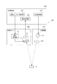
図1は、本発明に係る第一実施形態の分光測定装置の概略構成を示すブロック図である。
分光測定装置1は、本発明の電子機器であり、測定対象Xで反射された測定対象光に基づいて、測定対象光のスペクトルを測定する装置である。なお、本実施形態では、測定対象Xで反射した測定対象光を測定する例を示すが、測定対象Xとして、例えば液晶パネル等の発光体を用いる場合、当該発光体から発光された光を測定対象光としてもよい。
この分光測定装置1は、図1に示すように、光学モジュール10と、ディテクター11と、I−V変換器12と、アンプ13と、A/D変換器14と、制御部20と、を備えている。
[First embodiment]
Hereinafter, a first embodiment according to the present invention will be described with reference to the drawings.
[Configuration of Spectrometer 1]
FIG. 1 is a block diagram showing a schematic configuration of the spectrometer according to the first embodiment of the present invention.
The spectroscopic measurement device 1 is an electronic apparatus according to the present invention, and is a device that measures the spectrum of the measurement target light based on the measurement target light reflected by the measurement target X. In this embodiment, an example of measuring the measurement target light reflected by the measurement target X is shown. However, when a light emitter such as a liquid crystal panel is used as the measurement target X, the light emitted from the light emitter is measured. The target light may be used.
As shown in FIG. 1, the spectrometer 1 includes an
ディテクター11は、光学モジュール10の波長可変干渉フィルター5を透過した光を受光し、受光した光の光強度に応じた検出信号(電流)を出力する。
I−V変換器12は、ディテクター11から入力された検出信号を電圧値に変換し、アンプ13に出力する。
アンプ13は、I−V変換器12から入力された検出信号に応じた電圧(検出電圧)を増幅する。
A/D変換器14は、アンプ13から入力された検出電圧(アナログ信号)をデジタル信号に変換し、制御部20に出力する。
The detector 11 receives the light transmitted through the wavelength
The
The
The A /
[光学モジュール10の構成]
次に、光学モジュール10の構成について、以下に説明する。
光学モジュール10は、図1に示すように、波長可変干渉フィルター5と、ギャップ制御部15とを備えて構成される。
[Configuration of Optical Module 10]
Next, the configuration of the
As shown in FIG. 1, the
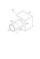
(波長可変干渉フィルター5の構成)
図2は、波長可変干渉フィルター5の概略構成を示す断面図である。
本実施形態の波長可変干渉フィルター5は、いわゆるファブリーペローエタロンである。この波長可変干渉フィルター5は、図2に示すように、固定基板51と、可動基板52とを備えている。これらの固定基板51及び可動基板52は、それぞれ例えば各種ガラスや、水晶、シリコンなどにより形成されている。そして、これらの固定基板51及び可動基板52は、固定基板51の第一接合部513及び可動基板の第二接合部523が、例えばシロキサンを主成分とするプラズマ重合膜などにより構成された接合膜53により接合されることで、一体的に構成されている。
(Configuration of wavelength variable interference filter 5)
FIG. 2 is a cross-sectional view showing a schematic configuration of the variable
The variable
固定基板51には、固定反射膜54(第一反射膜)が設けられ、可動基板52には、可動反射膜55(第二反射膜)が設けられており、これらの固定反射膜54および可動反射膜55は、反射膜間ギャップG1(ギャップ)を介して対向配置されている。そして、波長可変干渉フィルター5には、この反射膜間ギャップG1の大きさ(反射膜54,55間の距離,隙間寸法)を調整(変更)するのに用いられる静電アクチュエーター56が設けられている。この静電アクチュエーター56は、固定基板51に設けられた固定電極561と、可動基板52に設けられた可動電極562とにより構成されている。これらの固定電極561,可動電極562は、電極間ギャップを介して対向し、静電アクチュエーター56(ギャップ変更部)として機能する。ここで、これらの固定電極561,可動電極562は、それぞれ固定基板51及び可動基板52の基板表面に直接設けられる構成であってもよく、他の膜部材を介して設けられる構成であってもよい。なお、図2では、電極間ギャップの隙間寸法が、反射膜間ギャップG1の隙間寸法より大きい例を示すが、電極間ギャップが反射膜間ギャップG1よりも小さくなる構成などとしてもよい。
The fixed
以下、波長可変干渉フィルター5の構成についてより詳細に説明する。
固定基板51には、エッチングにより電極設置溝511および反射膜設置部512が形成されている。この固定基板51は、可動基板52に対して厚み寸法が大きく形成されており、静電アクチュエーター56に電圧を印加した際の静電引力や、固定電極561の内部応力による固定基板51の撓みはない。
Hereinafter, the configuration of the wavelength
In the fixed
電極設置溝511は、例えば、固定基板51の平面中心点を中心とした環状に形成されている。反射膜設置部512は、前記平面視において、電極設置溝511の中心から可動基板52側に突出して形成されている。この電極設置溝511の溝底面は、固定電極561が配置される電極設置面511Aとなる。また、反射膜設置部512の突出先端面は、反射膜設置面512Aとなる。
また、図示は省略するが、固定基板51には、電極設置溝511から、固定基板51の外周縁に向かって延出する電極引出溝が設けられており、電極設置溝511に設けられた固定電極561の引出電極が設けられている。
The
Although not shown, the fixed
電極設置溝511の電極設置面511Aには、固定電極561が設けられている。より具体的には、固定電極561は、電極設置面511Aのうち、後述する可動部521の可動電極562に対向する領域に設けられている。また、固定電極561上に、固定電極561及び可動電極562の間の絶縁性を確保するための絶縁膜が積層される構成としてもよい。また、固定電極561には、固定引出電極が接続されており、この固定引出電極は、上述した電極引出溝から固定基板51の外周部に引き出され、ギャップ制御部15に接続されている。
A fixed
なお、本実施形態では、電極設置面511Aに1つの固定電極561が設けられる構成を示すが、例えば、平面中心点を中心とした同心円となる2つの電極が設けられる構成(二重電極構成)などとしてもよい。
In the present embodiment, a configuration in which one fixed
反射膜設置部512は、上述したように、電極設置溝511と同軸上で、電極設置溝511よりも小さい径寸法となる略円柱状に形成され、当該反射膜設置部512の可動基板52に対向する反射膜設置面512Aを備えている。
この反射膜設置部512には、固定反射膜54が設置されている。この固定反射膜54としては、例えばAg等の金属膜や、Ag合金等の合金膜を用いることができる。また、例えば高屈折層をTiO2、低屈折層をSiO2とした誘電体多層膜を用いてもよい。さらに、誘電体多層膜上に金属膜(又は合金膜)を積層した反射膜や、金属膜(又は合金膜)上に誘電体多層膜を積層した反射膜、単層の屈折層(TiO2やSiO2等)と金属膜(又は合金膜)とを積層した反射膜などを用いてもよい。
As described above, the reflective
A fixed
また、固定基板51の光入射面(固定反射膜54が設けられない面)には、固定反射膜54に対応する位置に反射防止膜を形成してもよい。この反射防止膜は、低屈折率膜および高屈折率膜を交互に積層することで形成することができ、固定基板51の表面での可視光の反射率を低下させ、透過率を増大させる。
Further, an antireflection film may be formed at a position corresponding to the fixed
可動基板52は、平面中心点を中心とした円形状の可動部521と、可動部521と同軸であり可動部521を保持する保持部522と、保持部522の外側に設けられた基板外周部525と、を備えている。
The
可動部521は、保持部522よりも厚み寸法が大きく形成され、例えば、本実施形態では、可動基板52の厚み寸法と同一寸法に形成されている。この可動部521は、フィルター平面視において、少なくとも反射膜設置面512Aの外周縁の径寸法よりも大きい径寸法に形成されている。そして、この可動部521には、可動電極562及び可動反射膜55が設けられている。
なお、固定基板51と同様に、可動部521の固定基板51とは反対側の面には、反射防止膜が形成されていてもよい。このような反射防止膜は、低屈折率膜および高屈折率膜を交互に積層することで形成することができ、可動基板52の表面での可視光の反射率を低下させ、透過率を増大させることができる。
The
Similar to the fixed
可動電極562は、電極間ギャップを介して固定電極561に対向し、固定電極561と同一形状となる環状に形成されている。また、図示は省略するが、可動基板52には、可動電極562の外周縁から可動基板52の外周縁に向かって延出する可動引出電極が設けられている。この可動引出電極は、固定引出電極と同様に、ギャップ制御部15に接続される。
可動反射膜55は、可動部521の可動面521Aの中心部に、固定反射膜54と反射膜間ギャップG1を介して対向して設けられる。この可動反射膜55としては、上述した固定反射膜54と同一の構成の反射膜が用いられる。
The
The movable
保持部522は、可動部521の周囲を囲うダイアフラムであり、可動部521よりも厚み寸法が小さく形成されている。このような保持部522は、可動部521よりも撓みやすく、僅かな静電引力により、可動部521を固定基板51側に変位させることが可能となる。この際、可動部521が保持部522よりも厚み寸法が大きく、剛性が大きくなるため、保持部522が静電引力により固定基板51側に引っ張られた場合でも、可動部521の形状変化が起こらない。したがって、可動部521に設けられた可動反射膜55の撓みも生じず、固定反射膜54及び可動反射膜55を常に平行状態に維持することが可能となる。
なお、本実施形態では、ダイアフラム状の保持部522を例示するが、これに限定されず、例えば、平面中心点を中心として、等角度間隔で配置された梁状の保持部が設けられる構成などとしてもよい。
The holding
In the present embodiment, the diaphragm-
基板外周部525は、上述したように、フィルター平面視において保持部522の外側に設けられている。この基板外周部525の固定基板51に対向する面は、第一接合部513に対向する第二接合部523を備え、第二接合部523は、接合膜53により第一接合部513に接合されている。
As described above, the substrate outer
(ギャップ制御部15の構成)
ギャップ制御部15は、図1に示すように、記憶部16と、電圧制御部17と、を備えている。
記憶部16は、例えばROMやRAM等の半導体メモリーにより構成されている。この記憶部16には、波長可変干渉フィルター5により取り出す光の波長(測定対象波長)と、静電アクチュエーター56に印加する電圧との関係を示すV−λデータが記憶される。
ここで、表1に、波長可変干渉フィルター5を透過する光の波長と、反射膜間ギャップG1との関係を示す。なお、ここでは、固定反射膜54はAg合金を用いた場合を想定している。また、表2に、本実施形態における測定対象波長と、当該測定対象波長の光を取り出すための反射膜間ギャップG1との関係の一例を示す。
(Configuration of Gap Control Unit 15)
As shown in FIG. 1, the
The
Here, Table 1 shows the relationship between the wavelength of light transmitted through the wavelength

本実施形態では、V−λデータとして、表2に示すように、波長400nm〜480nm(第一波長域)に対して2次ピーク波長に対応した反射膜間ギャップG1の隙間寸法340.1nm〜423.0nmを設定するための電圧値が記録され、波長500nm〜700nm(第二波長域)に対して1次ピーク波長に対応した反射膜間ギャップG1の隙間寸法193.6nm〜296.1nmを設定するための電圧値が記録されている。
なお、本実施形態では、測定対象波長に対する電圧をV−λデータに記録する例を示したが、これに限定されず、測定対象波長に対して、電圧及び反射膜間ギャップG1が関連付けられたデータが用いられてもよい。さらに、表2に示すような測定対象波長に対する反射膜間ギャップG1との関係を示すG−λデータと、反射膜間ギャップG1に対する電圧を示すV−Gデータとが記録されてもよい。
In this embodiment, as V-λ data, as shown in Table 2, with respect to wavelengths of 400 nm to 480 nm (first wavelength range), the gap dimension G34 between the reflective films corresponding to the secondary peak wavelength is 340.1 nm to 34 nm. A voltage value for setting 423.0 nm is recorded, and a gap size of 193.6 nm to 296.1 nm of the gap G1 between the reflective films corresponding to the primary peak wavelength with respect to a wavelength of 500 nm to 700 nm (second wavelength range) is set. The voltage value for setting is recorded.
In the present embodiment, an example in which the voltage for the wavelength to be measured is recorded in the V-λ data is shown, but the present invention is not limited to this, and the voltage and the gap G1 between the reflection films are associated with the wavelength to be measured. Data may be used. Further, G-λ data indicating the relationship between the reflection film gap G1 with respect to the measurement target wavelength as shown in Table 2 and VG data indicating the voltage with respect to the reflection film gap G1 may be recorded.
電圧制御部17は、制御部20、記憶部16及び波長可変干渉フィルター5の静電アクチュエーター56に接続され、制御部20からの指令に基づいて静電アクチュエーター56に印加する電圧を変化させ、反射膜間ギャップG1を制御する。
具体的には、電圧制御部17は、制御部20から測定対象波長を指定する指令が入力されると、記憶部16のV−λデータから指定された測定対象波長に対応する電圧値を取得し、波長可変干渉フィルター5の静電アクチュエーター56に電圧を印加する。これにより、上記表2に示すように、静電アクチュエーター56により、測定対象波長に対する反射膜間ギャップG1の隙間寸法が設定される。
The
Specifically, when a command for designating the measurement target wavelength is input from the
[制御部20の構成]
図1に戻り、分光測定装置1の制御部20について、説明する。
制御部20は、本発明の処理部に相当し、例えばCPUやメモリー等が組み合わされることで構成され、分光測定装置1の全体動作を制御する。この制御部20は、図1に示すように、フィルター駆動部21と、光量取得部22と、分光測定部23と、を備えている。
[Configuration of Control Unit 20]
Returning to FIG. 1, the
The
フィルター駆動部21は、光学モジュール10のギャップ制御部15に対して、所定の測定波長域の光を所定の測定ピッチで波長可変干渉フィルター5を透過させる旨の指令信号を出力する。
光量取得部22は、A/D変換器14から入力される信号(電圧)に基づいて、ディテクター11にて受光された光の光量(光強度)を取得する。
The filter drive unit 21 outputs a command signal to the effect that the light in a predetermined measurement wavelength region is transmitted through the wavelength
The light
分光測定部23は、光量取得部22により取得された光量に基づいて、測定対象光のスペクトル特性を測定する。
図3は、表2に対応したV−λデータに基づいて波長可変干渉フィルター5を駆動させる場合の、当該波長可変干渉フィルター5の透過率特性を示す図である。
表2に対応したV−λデータに基づいて波長可変干渉フィルター5を駆動させた場合では、上述のように、400nm〜480nm第一波長域に対して2次ピーク波長により測定対象波長の光を透過させ、500nm〜700nm第二波長域に対して1次ピーク波長により測定対象波長の光を透過させる。この場合、図3に示すように、第二波長域の測定対象波長の光を取り出す際に、第一波長域の光が同時に透過することはない。
しかしながら、高次のピーク波長を用いて測定対象波長を取り出す場合、測定対象波長とは異なるピーク波長の光が同時に取り出され、その分、ノイズ成分が含まれることになる。
例えば、第一波長域に対して3次ピーク波長により測定対象波長の光を透過させ、第二波長域に対して2次ピーク波長により測定対象波長の光を透過させる場合では、表1に示すように、例えば波長400nmの光を3次ピーク波長として取り出す際に、波長600nm近傍の光が2次ピーク波長として同時に取り出される。同様に、第二波長域の測定対象波長を取り出す場合でも、3次ピーク波長として第一波長域の光が取り出されてしまう。
したがって、分光測定部23は、測定対象Xにより反射された光の分光スペクトルを得るために、光量取得部22により得られた複数の測定対象波長に対する光量から、分光スペクトルを推定するスペクトル推定処理を実施する。また、光量取得部22により取得される光量は、厳密には測定対象波長の光のみの光量ではなく、測定対象波長を中心とした所定波長幅の光も含まれる。このため、表2に示すようなV−λデータに基づいて波長可変干渉フィルター5から光を取り出した場合でも、分光測定部23によりスペクトル推定処理を実施することが好ましい。
The
FIG. 3 is a diagram showing the transmittance characteristics of the
In the case where the wavelength
However, when a measurement target wavelength is extracted using a higher-order peak wavelength, light having a peak wavelength different from the measurement target wavelength is extracted at the same time, and a noise component is included accordingly.
For example, Table 1 shows the case where light of the measurement target wavelength is transmitted by the tertiary peak wavelength with respect to the first wavelength range and light of the measurement target wavelength is transmitted by the secondary peak wavelength with respect to the second wavelength range. Thus, for example, when light having a wavelength of 400 nm is extracted as a tertiary peak wavelength, light in the vicinity of a wavelength of 600 nm is simultaneously extracted as a secondary peak wavelength. Similarly, even when the measurement target wavelength in the second wavelength range is extracted, the light in the first wavelength range is extracted as the tertiary peak wavelength.
Therefore, in order to obtain the spectral spectrum of the light reflected by the measurement target X, the
以下に、分光測定部23におけるスペクトル推定処理の一例を説明する。
分光測定部23は、以下に示す式(2)のように、光量取得部22により得られた計測スペクトル(各測定対象波長に対する光量)Dに対して、例えばメモリー等の記憶手段(図示略)に記憶された推定行列Ms(変換行列)を作用させることで、測定対象光(測定対象Xにより反射された光)の分光スペクトルSを推定する。
なお、推定行列Msは、分光測定装置1により、正確な分光スペクトルS0が予め測定されている基準光を計測し、この計測により得られた計測スペクトルD0と、正確な分光スペクトルS0とから、算出される。
Below, an example of the spectrum estimation process in the
The
Note that the estimation matrix Ms is obtained by measuring the reference light in which the accurate spectral spectrum S 0 is measured in advance by the spectroscopic measurement device 1, and the measurement spectrum D 0 obtained by this measurement and the accurate spectral spectrum S 0 . Is calculated from
![]()
![]()
上記式(2)において、「t」は、転置ベクトルを示している。式(2)において、分光スペクトルS及び計測スペクトルDは、「行ベクトル」で示されることから、これらの転置ベクトルは「列ベクトル」となる。
上記式(2)を、各要素を明示した状態で示すと、式(3)のようになる。
In the above equation (2), “t” represents a transposed vector. In the equation (2), the spectral spectrum S and the measurement spectrum D are indicated by “row vectors”, and thus these transposed vectors become “column vectors”.
When the above equation (2) is shown in a state where each element is clearly shown, the equation (3) is obtained.
上記式(3)において、計測スペクトルDは、分光測定装置1において計測する測定対象波長の数(バンド数)に相当する数の要素により構成される。表2に示す例では、測定波長域(400nm〜700nm)を20nmピッチで測定することから、上記式(3)では、d1〜d16の16個の要素から構成される。なお、これらのd1〜d16の要素は、それぞれ、各測定対象波長に対する光量取得部22により取得される光量となる。
また、分光スペクトルSは、推定しようとする波長の数(スペクトル点数)に相当する個数の要素から構成される。例えば、上記式(3)では、400nm〜700nmの対象波長域を5nmピッチの波長で分光スペクトルSを推定するべく、分光スペクトルSが行ベクトルの要素が61個に構成されている。
したがって、計測スペクトルDから分光スペクトルSを推定するための推定行列Msは、式(3)に示すように、61行×16列の行列となる。
ここで、計測スペクトルDの要素が16個であるのに対し、分光スペクトルSの要素が61個であるので、一組の計測スペクトルD及び分光スペクトルSだけでは、61行×16列の推定行列Msを決定することができない。したがって、この推定行列Msは、複数のサンプル光(予め分光スペクトルS0が計測されている基準光)を分光測定装置1により計測することで決定される。
In the above equation (3), the measurement spectrum D is composed of a number of elements corresponding to the number of measurement target wavelengths (number of bands) measured by the spectrometer 1. In the example shown in Table 2, since the measurement wavelength range (400 nm to 700 nm) is measured at a pitch of 20 nm, the above formula (3) is composed of 16 elements d1 to d16. Note that these elements d1 to d16 are light amounts acquired by the light
The spectral spectrum S is composed of a number of elements corresponding to the number of wavelengths to be estimated (the number of spectrum points). For example, in the above equation (3), the spectral spectrum S is composed of 61 row vector elements in order to estimate the spectral spectrum S at a wavelength of 5 nm pitch in the target wavelength range of 400 nm to 700 nm.
Therefore, the estimation matrix Ms for estimating the spectral spectrum S from the measured spectrum D is a matrix of 61 rows × 16 columns as shown in Expression (3).
Here, the number of elements of the measurement spectrum D is 16, whereas the number of elements of the spectral spectrum S is 61. Therefore, an estimated matrix of 61 rows × 16 columns can be obtained with only one set of the measurement spectrum D and the spectral spectrum S. Ms cannot be determined. Therefore, the estimation matrix Ms is determined by measuring a plurality of samples light (reference light pre-spectrum S 0 is measured) by the spectrometer 1.
このような推定行列Msは、次のように決定する。つまり、予め分光スペクトルSが計測されている複数のサンプル光(基準光)を分光測定装置1で測定して各サンプル光に対する計測スペクトルD0を取得する。
ここで、分光スペクトルSがスペクトル点数k(式(3)の場合では、61個)の要素を有するとし、サンプル数nのサンプル光を測定する場合、分光スペクトルS0は、次式(4)のように行列Stの形で表すことができる。また、計測スペクトルD0は、バンド数b(式(3)の場合では、16)の要素を持ち、サンプル数nのサンプル光に対してそれぞれ計測結果が得られる。したがって、計測スペクトルD0は、次式(5)のように行列Dtの形で表すことができる。
Such an estimation matrix Ms is determined as follows. That is, a plurality of sample lights (reference lights) for which the spectrum S is measured in advance are measured by the spectrometer 1 to obtain a measurement spectrum D 0 for each sample light.
Here, assuming that the spectral spectrum S has k number of spectral points (61 in the case of the formula (3)), and measuring the sample light of the number of samples n, the spectral spectrum S 0 is expressed by the following formula (4 ) it can be expressed in the form of a matrix S t as. Moreover, the measurement spectrum D 0 has an element of the number of bands b (16 in the case of the expression (3)), and a measurement result is obtained for each sample light of the number of samples n. Therefore, the measurement spectrum D 0 can be expressed in the form of a matrix D t as in the following equation (5).
そして、行列Stと、行列Dt及び推定行列Msの内積(Ms・Dt)との偏差を表す評価関数F(Ms)=|St−Ms・Dt|2を設定し、この評価関数F(Ms)が最小となるように推定行列Msを決定する。すなわち、評価関数F(Ms)を推定行列Msで偏微分した値が0となるため、推定行列Msは、下記式(6)により決定することができる。 Then, a matrix S t, the inner product of matrix D t and estimation matrix Ms (Ms · D t) evaluation function representing a difference between F (Ms) = | S t -Ms · D t | Set 2, this evaluation The estimation matrix Ms is determined so that the function F (Ms) is minimized. That is, since the value obtained by partial differentiation of the evaluation function F (Ms) with the estimation matrix Ms is 0, the estimation matrix Ms can be determined by the following equation (6).
![]()
![]()
なお、上記では、基準光であるサンプル光の分光スペクトルS0に誤差がないものとしたが、サンプル光の分光スペクトルS0の誤差を考慮した推定行列Msを決定してもよい。つまり、サンプル光の分光スペクトルS0は、マルチ分光測色計等の計測器を用いて測定されるが、当該計測器では、数nm程度の極めて狭い波長範囲の光を取り出して分光スペクトルS0を測定する。このように極めて狭い波長範囲を取り出す場合、光量が小さく、SN比が低くなるため、誤差が重畳しやすくなる。このような場合では、主成分分析法を用いると、行列Snkは、主成分数をj、主成分値をa、主成分ベクトルをvとして、「Snk=anj・vjk」として表すことができ、サンプル光の誤差を考慮した推定行列Msを算出することもできる。 In the above, the spectrum S 0 of the sample light is a reference light has been that there is no error, the error of spectrum S 0 of the sample light may determine the estimation matrix Ms considering. That is, the spectral spectrum S 0 of the sample light is measured using a measuring instrument such as a multi-spectral colorimeter, and the measuring instrument takes out light in an extremely narrow wavelength range of about several nanometers and takes the spectral spectrum S 0. Measure. When an extremely narrow wavelength range is taken out in this way, the amount of light is small and the SN ratio is low, so that errors are easily superimposed. In such a case, using the principal component analysis method, the matrix S nk is expressed as “S nk = a nj · v jk ” where j is the number of principal components, a is the principal component value, and v is the principal component vector. It is also possible to calculate the estimation matrix Ms in consideration of the error of the sample light.
なお、上記のスペクトル推定処理に限定されず、その他の推定処理を実施してもよい。
例えば、表2のように、波長可変干渉フィルター5を透過した光に複数のピーク波長が含まれない場合では、従来のスペクトル推定を用いることができる。すなわち、波長可変干渉フィルター5における分光感度特性(各測定対象波長に対する透過率特性)を予め検査して、メモリー(図示略)等の記憶手段に記憶しておき、当該分光感度特性と、取得した光量(計測光量)に基づいて分光スペクトルを推定することができる。
また、分光測定部23のスペクトル推定処理の方法としては、上述のような2つの方法に限られず、例えばウィナー推定法等を用いてもよい。
In addition, it is not limited to said spectrum estimation process, You may implement another estimation process.
For example, as shown in Table 2, when the light transmitted through the
Further, the spectrum estimation processing method of the
[分光測定装置1による分光測定処理]
図4は、分光測定装置1の分光測定処理を示すフローチャートである。
分光測定装置1により測定対象光の分光スペクトルを測定するためには、まず、制御部20のフィルター駆動部21は、光学モジュール10に対して波長可変干渉フィルター5を駆動させて、所定の測定波長域(例えば400nm〜700nm)に対して、所定の測定ピッチ(例えば20nm)で光を透過させる旨の指令信号を出力する(ステップS1)。
[Spectroscopic measurement processing by the spectroscopic measurement apparatus 1]
FIG. 4 is a flowchart showing the spectroscopic measurement process of the spectroscopic measurement apparatus 1.
In order to measure the spectral spectrum of the measurement target light by the spectroscopic measurement device 1, first, the filter driving unit 21 of the
ギャップ制御部15の電圧制御部17は、制御部20から指令信号が入力されると、記憶部16のV−λデータから各測定対象波長に対応する電圧値を読み込む(ステップS2)。そして、電圧制御部17は、読み込んだ電圧値を小さい順にソートし(ステップS3)、順次、波長可変干渉フィルター5の静電アクチュエーター56に電圧を印加する(ステップS4)。これにより、波長可変干渉フィルター5の反射膜間ギャップG1が初期ギャップから、隙間寸法が小さくなる方向に順次切り替えられ、各測定対象波長の光が順次透過される。したがって、表2のように、第一波長域に対して2次ピーク波長により測定対象波長の光を取り出し、第二波長域に対して1次ピーク波長により測定対象波長を取り出す場合、まず、第一波長域の600nmの光が2次ピーク波長として透過され、20nmピッチで透過波長が短くなる。そして、400nmの光が2次ピーク波長として透過された後、第二波長域の700nmの光が1次ピーク波長として透過される。そして、620nmの光が1次ピーク波長として透過されるまで、20nmピッチで透過波長が短くなる。
なお、光量取得部22は、波長可変干渉フィルター5を透過してディテクター11に受光された光の光量を順次取得し、メモリー等の記憶手段に記憶する。
When the command signal is input from the
The light
この後、ギャップ制御部15は、ステップS2で読み込んだ全ての電圧が印加されたか否かを判定する(ステップS5)。ステップS5において、「No」と判定された場合、つまり、印加する電圧が残っている場合、ステップS4に戻り、当該電圧を静電アクチュエーター56に印加して、対応する測定対象波長の光を透過させる。
一方、ステップS5において「Yes」と判定された場合、ギャップ制御部15は、波長可変干渉フィルター5の駆動を終了させる(ステップS6)。
この後、分光測定部23は、記憶手段に記憶された光量(計測スペクトルD)と、推定行列Msを用いて、スペクトル推定を実施する(ステップS7)。
Thereafter, the
On the other hand, when it is determined as “Yes” in Step S5, the
Thereafter, the
[波長可変干渉フィルター5を駆動させた際の反射膜間ギャップ]
次に、上記のような分光測定処理において、波長可変干渉フィルター5を駆動させた場合の、反射膜間ギャップG1の距離について説明する。
図5は、測定波長域の各測定対象波長の光を1次ピーク波長、及び2次ピーク波長の光として取り出した際の反射膜間ギャップの大きさを示す図である。
表2に対応したV−λデータを用いる場合、400nm〜480nmの第一波長域に対して、次数m=2である2次ピーク波長により測定対象波長の光を取出し、500nm〜700nmの第二波長域に対して、次数m=1である1次ピーク波長により測定対象波長の光を取り出す。この場合、図3に示すような透過率特性に基づいて、測定対象波長の光が透過される。
[Gap between reflection films when wavelength
Next, the distance of the inter-reflective film gap G1 when the wavelength
FIG. 5 is a diagram showing the size of the gap between the reflection films when light of each wavelength to be measured in the measurement wavelength region is extracted as light of the primary peak wavelength and the secondary peak wavelength.
When the V-λ data corresponding to Table 2 is used, light having a wavelength to be measured is extracted from the first wavelength range of 400 nm to 480 nm using the secondary peak wavelength of order m = 2, and the second wavelength of 500 nm to 700 nm. The light of the wavelength to be measured is extracted with the primary peak wavelength where the order m = 1 with respect to the wavelength range. In this case, light of the wavelength to be measured is transmitted based on the transmittance characteristic as shown in FIG.
つまり、第二波長域よりも短波長である第一波長域に対して、第二波長域よりも高次の2次ピーク波長を用いて測定対象波長の光を透過させることで、例えば、1次ピーク波長のみを用いて測定波長域(400nm〜700nm)の各測定対象波長の光を透過させる場合に比べて、反射膜間ギャップG1の最小値(波長400nmに対するギャップ)を大きくすることができる。
これにより、固定反射膜54及び可動反射膜55の反射膜間ギャップG1が過剰に小さくなることがなく、これらの固定反射膜54及び可動反射膜55の間に異物が挟まるリスクを低減することができる。
That is, by transmitting the light of the measurement target wavelength to the first wavelength range that is shorter than the second wavelength range using the secondary peak wavelength higher than the second wavelength range, for example, 1 Compared to transmitting light of each wavelength to be measured in the measurement wavelength range (400 nm to 700 nm) using only the next peak wavelength, the minimum value of the gap G1 between the reflection films (gap with respect to the wavelength of 400 nm) can be increased. .
Accordingly, the gap G1 between the
また、第一波長域よりも長波長である第二波長域に対して、第一波長域よりも低次の1次ピーク波長を用いて測定対象波長の光を透過させる。この場合、第二波長域に対するギャップ駆動量を低減させることができる。
すなわち、上述のように、固定反射膜54及び可動反射膜55の間に異物が挟まるリスクを低減するために、2次ピーク波長のみを用いて測定波長域の各測定対象波長の光を透過させる場合、表1及び図5に示すように、静電アクチュエーター56によるギャップ駆動範囲Gm2は、340.1nm〜646.0nmとなり、全ての測定対象波長の光を順次取り出すために可動部521を306.0nm駆動させる必要がある。
これに対して、本実施形態では、静電アクチュエーター56によるギャップ駆動範囲Gm´は、第一波長域に対するギャップ駆動範囲Gm2´である340.1nm〜423.0nm、及び第二波長域に対するギャップ駆動範囲Gm1´である193.6nm〜296.1nmとなる。この場合、全ての測定対象波長の光を順次取り出すために可動部521を駆動させる量(ギャップ駆動量)229.4nmであり、2次ピーク波長のみを用いる場合のギャップ駆動量(306.0nm)に比べて駆動量を小さくできる。
一般に、静電アクチュエーター56を用いた反射膜間ギャップG1の調整では、可動基板52の復元力に反して可動部521を変位させる必要があり、駆動量が大きいとその分復元力も大きくなり、ギャップ制御が困難となる。これに対して、上記のように、ギャップ駆動量が小さくなることで、ギャップ制御が容易となり、これに伴って反射膜間ギャップG1を精度よく所望の値に調整することが可能となる。また、ギャップ駆動量が大きい場合では、駆動に要する電力も増大するが、ギャップ駆動量が減少することで、駆動に要する電力も低減できる。
Moreover, the light of a measuring object wavelength is permeate | transmitted using the primary peak wavelength lower than the 1st wavelength range with respect to the 2nd wavelength range longer than the 1st wavelength range. In this case, the gap drive amount for the second wavelength region can be reduced.
That is, as described above, in order to reduce the risk of foreign matter being caught between the fixed
On the other hand, in this embodiment, the gap drive range G m ′ by the
In general, in the adjustment of the inter-reflective film gap G1 using the
[次数の設定]
上記の例では、表2に示すように、第一波長域の光を2次ピーク波長として透過させ、第二波長域の光を1次ピーク波長として透過させる例を示したが、他の次数を設定することも可能である。
例えば、以下の表3に示すように、第一波長域の光を3次ピーク波長として透過させ、第二波長域の光を2次ピーク波長として透過させてもよい。
[Order setting]
In the above example, as shown in Table 2, the example in which the light in the first wavelength range is transmitted as the secondary peak wavelength and the light in the second wavelength range is transmitted as the primary peak wavelength is shown. Can also be set.
For example, as shown in Table 3 below, light in the first wavelength range may be transmitted as the third peak wavelength, and light in the second wavelength range may be transmitted as the second peak wavelength.
表3のように、第一波長域に対して3次ピーク波長を用いて測定対象波長の光を透過させ、第二波長域に対して2次ピーク波長を用いる場合、反射膜間ギャップG1の最小値は、443.6nmとなる。2次ピーク波長のみを用いて測定波長域の各測定対象波長の光を透過させる場合、反射膜間ギャップG1の最小値は340.1nmとなるため、反射膜間ギャップG1の最小値をより大きくできる。したがって、反射膜間ギャップG1を狭めた際に、固定反射膜54及び可動反射膜55の間に異物が挟まるリスクをより低減できる。
As shown in Table 3, when the light of the wavelength to be measured is transmitted using the tertiary peak wavelength with respect to the first wavelength range and the secondary peak wavelength is used with respect to the second wavelength range, The minimum value is 443.6 nm. When transmitting light of each wavelength to be measured in the measurement wavelength region using only the secondary peak wavelength, the minimum value of the inter-reflection film gap G1 is 340.1 nm, and therefore the minimum value of the inter-reflection film gap G1 is made larger. it can. Therefore, when the gap G1 between the reflection films is narrowed, the risk of foreign matter being caught between the fixed
図6は、測定波長域の各測定対象波長の光を2次ピーク波長、及び3次ピーク波長の光として取り出した際の反射膜間ギャップの大きさを示す図である。
3次ピーク波長のみで測定対象波長の光を透過させる場合、表1及び図6に示すように、測定対象波長700nmに対応する反射膜間ギャップG1の隙間寸法996.1nmから、測定対象波長400nmに対応する反射膜間ギャップG1の隙間寸法540.2nmまでのギャップ駆動範囲Gm3だけ駆動させる必要があり、静電アクチュエーター56によるギャップ駆動量は、455.9nmとなる。
これに対して、第一波長域に対して3次ピーク波長を用いて測定対象波長の光を透過させ、第二波長域に対して2次ピーク波長を用いる場合、表1、表3、及び図6に示すように、第二波長域に属する測定対象波長のうちの最長波長に対応した反射膜間ギャップG1の大きさ(第二波長域における最大ギャップ)が、第一波長域に属する測定対象波長のうちの最短波長に対応した反射膜間ギャップG1の大きさ(第一波長域における最小ギャップ)よりも大きくなる。この場合、第一波長域のギャップ駆動範囲Gm3´´(540.2nm〜662.9nm)の一部と、第二波長域のギャップ駆動範囲Gm2´´(443.6nm〜646.0nm)の一部とが重なり合う。したがって、第一波長域のギャップ駆動範囲Gm3´´の一部の範囲で、第二波長域の一部の範囲の測定対象波長の光量をも取得することができる。このような場合、静電アクチュエーター56によるギャップ駆動範囲Gm´´は443.6nm〜662.9nmとなり、ギャップ駆動量は219.3nmとなるので、3次ピーク波長のみを用いて各測定対象波長の光量を取得する場合のギャップ駆動量(455.9nm)に比べて、小さくなる。
なお、このような場合では、第一波長域内の3次ピーク波長の光と、第二波長域内の2次ピーク波長の光とが同時に透過されることになる。このような場合でも、本実施形態では、分光測定部23によりスペクトル推定処理を実施することで、測定対象波長以外の光をカットした精度の高い分光スペクトルSを推定することができる。
FIG. 6 is a diagram illustrating the size of the gap between the reflection films when light of each measurement target wavelength in the measurement wavelength region is extracted as light of the secondary peak wavelength and the tertiary peak wavelength.
When transmitting light of the wavelength to be measured with only the third peak wavelength, as shown in Table 1 and FIG. 6, from the gap size 996.1 nm of the gap G1 between the reflective films corresponding to the wavelength of 700 nm, the wavelength to be measured is 400 nm. It is necessary to drive only the gap driving range G m3 up to the gap size 540.2 nm of the gap G1 between the reflection films corresponding to the above, and the gap driving amount by the
On the other hand, when transmitting the light of a measurement object wavelength using a tertiary peak wavelength with respect to a 1st wavelength range, and using a secondary peak wavelength with respect to a 2nd wavelength range, Table 1, Table 3, and As shown in FIG. 6, the size of the gap G1 between reflection films corresponding to the longest wavelength among the wavelengths to be measured belonging to the second wavelength range (the maximum gap in the second wavelength range) belongs to the first wavelength range. It becomes larger than the size of the gap G1 between the reflection films corresponding to the shortest wavelength among the target wavelengths (minimum gap in the first wavelength region). In this case, a part of the gap driving range G m3 ″ (540.2 nm to 662.9 nm) in the first wavelength region and the gap driving range G m2 ″ (443.6 nm to 646.0 nm) in the second wavelength region. Part of Therefore, it is also possible to acquire the amount of light of the wavelength to be measured in the partial range of the second wavelength range in the partial range of the gap drive range G m3 ″ in the first wavelength range. In such a case, the gap drive range G m ″ by the
In such a case, the light of the third order peak wavelength in the first wavelength range and the light of the second order peak wavelength in the second wavelength range are transmitted at the same time. Even in such a case, in the present embodiment, the spectrum estimation process is performed by the
なお、表3では、第二波長域のギャップ駆動範囲Gm2´´の一部の範囲と、第一波長域のギャップ駆動範囲Gm3´´の一部の範囲とが重なる例を示したが、例えば、第二波長域のギャップ駆動範囲Gm2´´全体が第一波長域のギャップ駆動範囲Gm3´´に含まれるように、第一波長域と第二波長域との範囲、及び各波長域に対する次数が設定されていてもよい。この場合でも、上記と同様に、重なり合ったギャップ駆動範囲において、第一波長域に属する測定対象波長の光と、第二波長域に属する測定対象波長の光との双方を透過させることが可能となり、ギャップ駆動量を効果的に低減させることができる。 Table 3 shows an example in which a part of the second wavelength band gap driving range G m2 ″ overlaps with a part of the first wavelength band gap driving range G m3 ″. For example, the range of the first wavelength range and the second wavelength range so that the entire gap drive range G m2 ″ of the second wavelength range is included in the gap drive range G m3 ″ of the first wavelength range, and each The order for the wavelength band may be set. Even in this case, similarly to the above, it is possible to transmit both the light of the measurement target wavelength belonging to the first wavelength range and the light of the measurement target wavelength belonging to the second wavelength range in the overlapping gap driving range. The gap driving amount can be effectively reduced.
また、表2、表3に示す例に限られず、他の次数を採用してもよく、測定波長域を例えば3つ以上の波長域に分類し、これらの各波長域に対してそれぞれ次数を異ならせてもよい。例えば、400nm〜500nmの波長域に対して3次ピーク波長により測定対象波長の光を透過させ、520nm〜600nmの波長域に対して2次ピーク波長により測定対象波長の光を透過させ、620nm〜700nmの波長域に対して1次ピーク波長により測定対象波長の光を透過させるように、V−λデータが設定されていてもよい。 Moreover, it is not restricted to the example shown in Table 2 and Table 3, You may employ | adopt another order and classify | categorize a measurement wavelength range into three or more wavelength ranges, for example, and each order with respect to each of these wavelength ranges. It may be different. For example, the light of the measurement target wavelength is transmitted by the tertiary peak wavelength with respect to the wavelength range of 400 nm to 500 nm, and the light of the measurement target wavelength is transmitted by the secondary peak wavelength with respect to the wavelength range of 520 nm to 600 nm. V-λ data may be set so that light having a wavelength to be measured is transmitted with a primary peak wavelength in a wavelength range of 700 nm.
[第一実施形態の作用効果]
本実施形態では、波長可変干渉フィルター5は、固定反射膜54、可動反射膜55、及びこれらの反射膜54,55間の反射膜間ギャップG1を変更する静電アクチュエーター56を備える。そして、ギャップ制御部15は、反射膜間ギャップG1を、第一波長域及び第二波長域に対してそれぞれ設定された次数のピーク波長で、測定対象波長の光を透過させる隙間寸法に制御する。すなわち、本実施形態では、測定波長域の各測定対象波長の光に対して、低次ピーク波長として透過させる測定対象波長、高次ピーク波長として透過させる測定対象波長が設定されている。
このような構成では、次数が高い高次ピーク波長を用いて測定対象波長の光を透過させることで、次数が低い低次ピーク波長を用いて測定対象波長の光を透過させる場合に比べて、反射膜間ギャップG1を大きくできる。このため、異物が反射膜54,55に挟まるリスクを低減でき、これによる動作不良の発生を抑制できる。また、測定対象波長によっては十分に反射膜間ギャップG1が大きく、異物が反射膜54,55に挟まる可能性が低い場合があり、このような場合まで、高次のピーク波長を用いると、静電アクチュエーター56の制御が困難となる。これに対して、本実施形態では、このような測定対象波長に対しては、低次ピーク波長を用いて測定対象波長の光を透過させるので、例えば、高次ピーク波長のみを用いて測定波長域の各測定対象波長の光を透過させる場合に比べ、静電アクチュエーター56によるギャップ駆動量を低減でき、ギャップ制御の精度を向上させることができる。
[Operational effects of the first embodiment]
In the present embodiment, the variable
In such a configuration, by transmitting light of the wavelength to be measured using a high-order peak wavelength having a high order, the light of wavelength to be measured is transmitted using a low-order peak wavelength having a low order, The gap G1 between the reflection films can be increased. For this reason, it is possible to reduce the risk of foreign matter being caught between the
本実施形態では、測定対象波長に対する電圧を記録したV−λデータが記憶部16に記憶されている。そして、このV−λデータでは、測定対象波長に対して予め次数が設定されており、その次数に対応するピーク波長により当該測定対象波長を透過させるための電圧が当該測定対象波長に対応付けられて記録されている。
このため、ギャップ制御部15は、測定対象波長に対応する電圧値をV−λデータから読み込み、当該電圧値に対応した電圧を静電アクチュエーター56に印加するだけで、反射膜間ギャップG1の大きさを測定対象波長に応じて設定された次数に対応する大きさに制御することができる。
In the present embodiment, V-λ data in which the voltage for the wavelength to be measured is recorded is stored in the
For this reason, the
本実施形態では、ギャップ制御部15は、測定波長域の短波長側である第一波長域(例えば400nm〜480nm)に属する測定対象波長の光を2次ピーク波長として透過させ、長波長側である第二波長域(例えば500nm〜700nm)に属する測定対象波長の光を1次ピーク波長として透過させる。
このため、反射膜間ギャップG1の隙間寸法がより小さくなる短波長側において、隙間寸法を増大させることができるので、反射膜54,55間での異物の挟まりを効果的に抑制できる。更に、長波長域において、2次ピーク波長を用いることで、静電アクチュエーター56によりギャップ駆動量を低減でき、ギャップ制御における制御の向上を図ることができる。
In the present embodiment, the
For this reason, since the gap dimension can be increased on the short wavelength side where the gap dimension of the gap G1 between the reflection films becomes smaller, it is possible to effectively suppress the trapping of foreign substances between the
本実施形態では、表3に示すように、第二波長域に属する測定対象波長の最長波長に対する反射膜間ギャップG1の隙間寸法が、第一波長域に属する測定対象波長の最短波長に対する反射膜間ギャップG1の隙間寸法よりも大きく設定されていてもよい。
このような場合では、第一波長域に対するギャップ駆動範囲のうちの少なくとも一部と、第二波長域に対するギャップ駆動範囲の少なくとも一部とが重なり合う。例えば、上記表3に示すように、第一波長域の測定対象波長の光を3次ピーク波長として透過させ、第二波長域の測定対象波長の光を2次ピーク波長として透過させる場合では、第二波長域に対するギャップ駆動範囲の一部(545.0nm〜646.0nm)が、第一波長域に対するギャップ駆動範囲(540.2nm〜662.9nm)に重なる。
したがって、重なり合った駆動範囲において、第一波長域の測定対象波長と、第二波長域の測定対象波長との双方を透過させることが可能となり、静電アクチュエーター56のギャップ駆動量をさらに低減させることができる。例えば、上記表1に示すように、3次ピーク波長のみにより各測定対象波長の光を透過させる場合では、表1に示すように、測定対象波長700nmに対応する996.1nmから、測定対象波長400nmに対応する540.2nmまで、455.9nm駆動させる必要がある。これに対して、本実施形態では、表3に示すように、測定対象波長480nmに対応する662.9nmから、測定対象波長500nmに対応する443.6nmまで219.3nm駆動させる間に、各測定対象波長の光も透過させることができる。
In this embodiment, as shown in Table 3, the gap size of the gap G1 between the reflection films with respect to the longest wavelength of the measurement target wavelength belonging to the second wavelength range is the reflection film with respect to the shortest wavelength of the measurement target wavelength belonging to the first wavelength range. It may be set larger than the gap size of the gap G1.
In such a case, at least a part of the gap driving range for the first wavelength region overlaps at least a part of the gap driving range for the second wavelength region. For example, as shown in Table 3 above, in the case where the light of the wavelength to be measured in the first wavelength range is transmitted as the tertiary peak wavelength, and the light of the wavelength to be measured in the second wavelength range is transmitted as the secondary peak wavelength, A part of the gap driving range for the second wavelength range (545.0 nm to 646.0 nm) overlaps with the gap driving range for the first wavelength range (540.2 nm to 662.9 nm).
Therefore, it is possible to transmit both the measurement target wavelength in the first wavelength range and the measurement target wavelength in the second wavelength range in the overlapping drive range, and further reduce the gap drive amount of the
本実施形態では、ギャップ制御部15の電圧制御部17は、ステップS2において、各測定対象波長に対する電圧値を読み込んだ後、ステップS3において、読み込んだ電圧値を小さい順にソートし、ソート順に電圧を順次、静電アクチュエーター56に印加する。
このため、反射膜間ギャップG1は、初期ギャップから順次隙間寸法が小さくなる方向に狭められ、可動部521を1ストローク駆動させることで、各測定対象波長に対する光量を取得することができる。
In this embodiment, the
For this reason, the gap G1 between the reflection films is narrowed in the direction in which the gap size is gradually reduced from the initial gap, and the light quantity for each wavelength to be measured can be acquired by driving the
そして、本実施形態の分光測定装置1では、分光測定部23は、得られた複数の測定対象波長に対する光量に基づいた計測スペクトルDに対して、推定行列Msを作用させることで、測定対象Xにより反射された測定光の分光スペクトルSを推算する。
このような推定行列Msは、分光スペクトルS0が既知である基準光(サンプル光)を分光測定装置1により測定した計測スペクトルD0と、分光スペクトルS0とに基づいて、計測スペクトルD0及び推定行列Msの内積と、分光スペクトルS0との偏差が最小となるように、設定される行列である。したがって、波長可変干渉フィルター5を透過する光に、測定対象波長の光以外のノイズ成分(例えば他のピーク波長の光)が含まれる場合であっても、計測スペクトルDに対して推定行列Msを作用させることで、精度の高い分光スペクトルSを推算することができる。
In the spectroscopic measurement apparatus 1 according to the present embodiment, the
Such estimation matrix Ms is the measured spectrum D 0 measured spectrum S 0 is the reference light are known (sample light) by the spectroscopic measurement device 1, based on the spectrum S 0, measured spectrum D 0 and and inner product of the estimated matrix Ms, so that the deviation between the spectrum S 0 is minimized is a matrix that is set. Therefore, even if the light transmitted through the wavelength
[第二実施形態]
次に、本発明に係る第二実施形態について、以下説明する。
上述した第一実施形態では、ギャップ制御部15は、測定対象波長に応じて、用いるピーク波長の次数が異なるようにV−λデータを設定し、このV−λデータに基づいて測定対象波長に対応する電圧を静電アクチュエーター56に印加した。これに対して、本実施形態では、ギャップ制御部は、測定対象波長に応じて次数を選択し、選択した次数に対応した反射膜間ギャップG1に設定するように静電アクチュエーター56を制御する点で、上記第一実施形態と相違する。
[Second Embodiment]
Next, a second embodiment according to the present invention will be described below.
In the first embodiment described above, the
図7は、第二実施形態の分光測定装置1Aの概略構成を示すブロック図である。
図7に示すように、本実施形態の分光測定装置1Aの光学モジュール10Aは、波長可変干渉フィルター5と、ギャップ制御部15Aとを備えている。また、ギャップ制御部15Aは、記憶部16と、電圧制御部17と、次数選択部18と、を備えている。
ここで、本実施形態の記憶部16には、波長可変干渉フィルター5から各測定対象波長の光を、各次数のピーク波長で透過させる際のギャップに対応する電圧を示すV−λデータが記憶されている。つまり、上述した表1の反射膜間ギャップG1の各隙間寸法に対する電圧が記録される。例えば測定対象波長λ1に対して、1次ピーク波長として当該測定対象波長λ1の光を取り出すための電圧、2次ピーク波長として当該測定対象波長λ1の光を取り出す電圧、3次ピーク波長として当該測定対象波長λ1の光を取り出す電圧、4次ピーク波長として当該測定対象波長λ1の光を取り出す電圧等が記録される。
FIG. 7 is a block diagram showing a schematic configuration of the
As shown in FIG. 7, the
Here, the
次数選択部18は、測定対象波長に対応した次数を選択する。
そして、電圧制御部17は、測定対象波長、及び次数選択部18により選択された次数に対応する電圧値を、記憶部16に記憶されるV−λデータから読み出し、読み出した電圧値に対応した電圧を静電アクチュエーター56に印加する。
The
Then, the
[次数選択部18による次数選択処理]
本実施形態では、上述のように、次数選択部18により、波長域毎の次数を選択することができる。
ここで、次数選択部18により選択される次数としては、各測定対象波長によって予め設定されていてもよく、例えば、測定者により適宜設定可能としてもよい。また、波長可変干渉フィルター5が設置される環境等の条件(例えば気圧や温度等)に応じて設定されるものであってもよい。
測定者により設定される場合には、例えば、図示略の操作部の入力操作に基づいて次数を取得する。
また、環境等の条件として、周囲の気圧や温度等を条件とする場合、分光測定装置1Aは、気圧計や温度計等の環境計測装置を備える構成とする。そして、環境計測装置により計測される値が、例えば、予め設定された閾値を超える場合に、初期値として設定された次数を「1」増加させるなどの処理をしてもよい。
[Order Selection Processing by Order Selector 18]
In the present embodiment, as described above, the
Here, the order selected by the
When set by the measurer, for example, the order is acquired based on an input operation of an operation unit (not shown).
Further, when the ambient pressure, temperature, or the like is used as a condition such as the environment, the
更に、次数選択部18は、波長可変干渉フィルター5の製造時のばらつきに応じて、次数を選択する。
すなわち、波長可変干渉フィルター5において、静電アクチュエーター56に電圧を印加していない初期状態における反射膜間ギャップG1の初期寸法は、製造上のばらつきを有する。このため、従来、測定を開始する測定開始寸法は、製造時における初期寸法のばらつきを考慮した上で、初期寸法よりも小さくなるように設定する必要があった。つまり、初期寸法が測定開始寸法よりも大きい場合では、まず、反射膜間ギャップG1が測定開始寸法となるまで、静電アクチュエーター56に電圧を印加して可動部521を変位させる必要があり、駆動量が大きくなるという課題があった。また、初期寸法が測定開始寸法よりも小さい場合では、静電アクチュエーター56により反射膜間ギャップG1を拡げることができないため、測定開始寸法に対応した測定対象波長の測定を実施することができないという課題があった
これに対して、本実施形態では、次数選択部18は、製造時における初期寸法に応じて、測定開始波長を選択する。これにより、測定対象波長に対して適切な次数を選択することで、初期寸法によらず、当該測定対象波長の光を取り出すことができ、また、駆動量の増大を抑制することも可能となる。
Further, the
That is, in the wavelength
以下、具体例を用いて、波長可変干渉フィルター5の製造時に生じる初期寸法のばらつきに対応した次数選択部18による次数選択方法について説明する。
下記に示す表4は、上述した第一実施形態の分光測定装置1において、初期寸法を450nm、430nm、410nmに設定した場合、波長域400nm〜700nmの測定が実施可能であるか否か、又、実施可能である場合でのギャップ駆動量を示す表である。
Hereinafter, the order selection method by the
Table 4 shown below shows whether or not measurement in the wavelength range of 400 nm to 700 nm can be performed when the initial dimension is set to 450 nm, 430 nm, and 410 nm in the spectroscopic measurement apparatus 1 of the first embodiment described above. It is a table | surface which shows the gap drive amount in the case where it can implement.
表2に対応したV−λデータを用いる場合では、測定開始寸法は、測定対象波長480nmに対応した423.0nmとなる。したがって、表4に示すように、初期寸法が410nmである場合では、測定対象波長480nmの光を2次ピーク波長として取り出せず、測定が実施できない。また、初期ギャップ450nmの場合では、まず、反射膜間ギャップG1を初期寸法から測定開始寸法である423.0nmまで駆動させた後、各測定対象波長に対応した隙間寸法に変化させる必要があるので、その分、ギャップ駆動量が増大する。 In the case of using V-λ data corresponding to Table 2, the measurement start dimension is 423.0 nm corresponding to the measurement target wavelength of 480 nm. Therefore, as shown in Table 4, in the case where the initial dimension is 410 nm, light having a measurement target wavelength of 480 nm cannot be extracted as the secondary peak wavelength, and measurement cannot be performed. In the case of the initial gap of 450 nm, first, after driving the gap between reflection films G1 from the initial dimension to the measurement start dimension of 423.0 nm, it is necessary to change to the gap dimension corresponding to each wavelength to be measured. Accordingly, the gap driving amount increases.
表5は、本実施形態において、初期寸法が450nm、430nm、410nmに設定されている場合における、波長域400nm〜700nmの測定が実施可能であるか否か、又、実施可能である場合でのギャップ駆動量を示す表である。また、表6は、初期寸法が450nmである場合に、次数選択部18により選択される次数を示す表であり、表7は、初期寸法が430nmである場合に、次数選択部18により選択される次数を示す表であり、表8は、初期寸法が410nmである場合に、次数選択部18により選択される次数を示す表である。
Table 5 shows whether or not the measurement in the wavelength region of 400 nm to 700 nm is possible when the initial dimensions are set to 450 nm, 430 nm, and 410 nm in this embodiment. It is a table | surface which shows gap drive amount. Table 6 is a table showing orders selected by the
本実施形態において、反射膜間ギャップG1の初期寸法が430nmである場合では、表7に示すように、次数選択部18は、400nmから480nmまでを第一波長域と設定して次数「2」を選択し、500nmから700nmまでを第二波長域と設定して次数「1」を選択する。つまり、表2と同様の次数が選択されることになる。この場合は、第一実施形態と同様のギャップ駆動量となる。
In this embodiment, when the initial dimension of the inter-reflective film gap G1 is 430 nm, as shown in Table 7, the
一方、本実施形態において初期寸法が450nmである場合、次数選択部18は、表6に示すように、400nmから500nmまでを第一波長域と設定して次数「2」を選択し、520nmから700nmまでを第二波長域と設定して次数「1」を選択する。つまり、第一波長域(400nm〜500nm)内の測定対象波長の光を2次ピーク波長として取出し、第二波長域(520nm〜700nm)内の測定対象波長の光を1次ピーク波長として取り出す。この場合、表2のパターンとは異なり、測定対象波長500nmの光が2次ピーク波長として取り出されることになる。
上述した第一実施形態の分光測定装置1では、初期寸法が450nmである場合、まず、測定開始寸法の423.0nmまで、27.0nm分だけ駆動させる必要が生じるが、本実施形態では、反射膜間ギャップG1を、初期寸法である450nmから、測定対象波長500nmに対応した443.6nmまで、6.4nmだけ駆動させた後、各測定対象波長に対応する寸法に変化させればよい。したがって、表5に示すように、ギャップ駆動量は、246.0nmとなり、第一実施形態の分光測定装置1を用いた場合のギャップ駆動量(256.4nm)に比べて小さくなる。
On the other hand, when the initial dimension is 450 nm in this embodiment, the
In the above-described spectroscopic measurement apparatus 1 according to the first embodiment, when the initial dimension is 450 nm, first, it is necessary to drive the measurement start dimension to 423.0 nm by 27.0 nm. The inter-film gap G1 may be driven by 6.4 nm from the initial dimension of 450 nm to 443.6 nm corresponding to the measurement target wavelength of 500 nm, and then changed to a dimension corresponding to each measurement target wavelength. Therefore, as shown in Table 5, the gap drive amount is 246.0 nm, which is smaller than the gap drive amount (256.4 nm) when the spectroscopic measurement apparatus 1 of the first embodiment is used.
また、第一実施形態の分光測定装置1では、反射膜間ギャップG1の初期寸法が410nmの場合、測定対象波長480nmの光を取り出すことができず、測定を実施することができない。これに対して、本実施形態では、初期寸法が410nmの場合、表8に示すように、次数選択部18は、400nmから460nmまでを第一波長域と設定して次数「2」を選択し、480nmから700nmまでを第二波長域と設定して次数「1」を選択する。これにより、初期寸法が410nmである場合でも、400nm〜700nmの測定波長域の各測定対象波長の光を取り出すことができる。また、この場合、ギャップ駆動量は226.9nmとなる。
Further, in the spectroscopic measurement device 1 of the first embodiment, when the initial dimension of the inter-reflective film gap G1 is 410 nm, light having a measurement target wavelength of 480 nm cannot be extracted and measurement cannot be performed. On the other hand, in this embodiment, when the initial dimension is 410 nm, as shown in Table 8, the
以上に示すように、本実施形態では、次数選択部18により次数を選択することで、測定開始ギャップにマージンを持たせることができる。したがって、波長可変干渉フィルター5の製造時において、初期寸法にばらつきが生じた場合でも、その初期寸法に応じて最適な次数を選択することで、所定の測定波長域内の各測定対象波長の光を適切に取り出すことができる。また、ギャップ駆動量を小さくすることができ、静電アクチュエーター56によるギャップ制御の精度を向上させることができる。
As described above, in this embodiment, a margin can be provided in the measurement start gap by selecting the order by the
[分光測定装置1Aによる分光測定処理]
本実施形態の分光測定装置1Aは、上述した第一実施形態と略同様の方法により分光測定動作を実施する。
ここで、本実施形態では、図3のステップS2において、ギャップ制御部15Aの次数選択部18は、波長域毎の次数を選択する。
この次数の選択では、上記のような条件により次数を選択することができる。
例えば、初期寸法に応じて、第一波長域及び第二波長域を設定し、これらの第一波長域及び第二波長域に対してそれぞれ次数を選択する。この場合、初期寸法を検出するために、例えば、固定基板51及び可動基板52の間に、静電容量検出用電極を設ける構成などとしてもよい。
また、上述したように、測定者の操作等に応じて、選択する次数を変更してもよい。この場合、次数選択部18は、操作部の入力操作に応じて、自由に測定に用いる次数を選択することができ、例えば、第一波長域に対して次数m=3を選択し、第二波長域に対して次数m=2を選択することも可能となる。その他、波長可変干渉フィルター5の設置環境等を検出するセンサーが設けられている場合では、次数選択部18は、これらのセンターにより検出された環境に応じて、次数を選択してもよい。
この後、電圧制御部17は、各測定対象波長に対して、次数選択部18により選択された次数に対応する電圧をV−λデータから読み込む。
以降の処理については、上記第一実施形態と同様に、ステップS3からステップS7の処理を実施する。
[Spectral measurement processing by the
The
Here, in this embodiment, in step S2 of FIG. 3, the
In this order selection, the order can be selected according to the above conditions.
For example, a first wavelength range and a second wavelength range are set according to the initial dimensions, and orders are selected for these first wavelength range and second wavelength range, respectively. In this case, in order to detect the initial dimension, for example, a configuration may be adopted in which an electrode for detecting capacitance is provided between the fixed
Further, as described above, the order to be selected may be changed according to the operation of the measurer. In this case, the
Thereafter, the
As for the subsequent processing, the processing from step S3 to step S7 is performed as in the first embodiment.
[第二実施形態の作用効果]
本実施形態では、ギャップ制御部15Aは、次数選択部18及び電圧制御部17を備え、次数選択部18は、測定対象波長に応じた次数を選択し、電圧制御部17は、選択された次数に応じた電圧を静電アクチュエーター56に印加する。
この場合でも、上述した第一実施形態と同様に、波長可変干渉フィルター5において、測定対象波長に応じて適切な次数のピーク波長により光を透過させることができる。すなわち、反射膜間ギャップG1の隙間寸法が小さくなり、反射膜54,55の間に異物が挟まってしまうリスク等を低減でき、かつ、高次のピーク波長のみを用いて全測定対象波長を透過させる場合に比べて、静電アクチュエーター56によるギャップ制御の精度を向上させることができる。
[Operational effects of the second embodiment]
In the present embodiment, the
Even in this case, similarly to the first embodiment described above, the wavelength
また、本実施形態では、V−λデータに、各測定対象波長の光を各ピーク波長で透過させる際の電圧が記憶され、次数選択部18により次数を選択することができるので、測定中においても、次数を適宜変更することも可能となる。
例えば、第一波長域に対して1次ピーク波長を用いて測定を実施し、例えば反射膜54,55間に異物が挟まる等の不都合が生じた場合に、当該第一波長域に対する次数を2次に変更するといった動作を行うこともできる。
そして、次数選択部18は、上述したように、反射膜間ギャップG1の初期寸法に応じて、適切な波長域(第一波長域及び第二波長域)を設定し各波長域に対して次数を選択する。これにより、製造時において、波長可変干渉フィルター5の初期寸法にばらつきが生じた場合でも、測定波長域(例えば400nm〜700nm)内の各測定対象波長の光を適切に取り出すことができる。また、ギャップ駆動量を小さくすることができるため、静電アクチュエーター56によるギャップ制御の精度を向上させることができる。
In the present embodiment, the V-λ data stores the voltage at the time of transmitting light of each wavelength to be measured at each peak wavelength, and the
For example, when the measurement is performed using the primary peak wavelength with respect to the first wavelength range, and a problem such as a foreign matter being caught between the
And the
更に、本実施形態では、各測定対象波長に対して、それぞれ複数の次数により光量測定を実施することが可能となる。
この場合、例えば、1回目の測定において、第一波長域に対して2次ピーク波長を用いた光量測定、第二波長域に対して1次ピーク波長を用いた光量測定を実施し、これらの光量(計測スペクトル)に基づいた分光スペクトルの推算を行う。この後、2回目の測定において、第一波長域に対して3次ピーク波長を用いた光量測定、第二波長域に対して2次ピーク波長を用いた光量測定を実施し、これらの光量(計測スペクトル)に基づいた分光スペクトルの推算を行う。そして、1回目に推算された分光スペクトルと、2回目に推算された分光スペクトルに基づいて、例えばその平均を採ることで、測定対象の分光スペクトルとする処理を実施してもよい。
Furthermore, in the present embodiment, it is possible to perform light quantity measurement with a plurality of orders for each wavelength to be measured.
In this case, for example, in the first measurement, the light quantity measurement using the secondary peak wavelength for the first wavelength range, and the light quantity measurement using the primary peak wavelength for the second wavelength range are performed. The spectral spectrum is estimated based on the amount of light (measured spectrum). Thereafter, in the second measurement, the light quantity measurement using the tertiary peak wavelength is performed for the first wavelength range, and the light quantity measurement using the secondary peak wavelength is performed for the second wavelength range. The spectral spectrum is estimated based on the measured spectrum. And based on the spectral spectrum estimated in the 1st time and the spectral spectrum estimated in the 2nd time, you may implement the process which makes the spectral spectrum of a measuring object by taking the average, for example.
[その他の実施形態]
なお、本発明は前述の実施形態に限定されるものではなく、本発明の目的を達成できる範囲での変形、改良等は本発明に含まれるものである。
[Other Embodiments]
It should be noted that the present invention is not limited to the above-described embodiments, and modifications, improvements, and the like within the scope that can achieve the object of the present invention are included in the present invention.
例えば、上記第一及び第二実施形態において、測定波長域を400nm〜700nmとし、第一波長域を400nm〜600nm、第二波長域を620nm〜700nmとしたが、これに限定されない。例えば、第一波長域を400nm〜480nmとし、第二波長域を500nm〜700nmとしてもよく、第一波長域及び第二波長域の範囲は適宜設定することができる。高次ピーク波長により測定対象波長の光を取り出す短波長側(第一波長域)を狭くすることで、ギャップ駆動範囲をより小さくでき、静電アクチュエーター56によるギャップ駆動量も減少するため、ギャップ制御の精度を向上できる。逆に、高次のピーク波長で測定対象波長の光を取り出す第一波長域を広く設定することで、反射膜54,55間における異物の挟まりや、それによる不都合をより効果的に防ぐことができる。
また、測定波長域としても、より広範囲を対象としてもよく、より狭い範囲を対象としてもよい。
For example, in the first and second embodiments, the measurement wavelength range is 400 nm to 700 nm, the first wavelength range is 400 nm to 600 nm, and the second wavelength range is 620 nm to 700 nm. However, the present invention is not limited to this. For example, the first wavelength range may be 400 nm to 480 nm, the second wavelength range may be 500 nm to 700 nm, and the ranges of the first wavelength range and the second wavelength range can be set as appropriate. By narrowing the short wavelength side (first wavelength range) from which light of the measurement target wavelength is extracted by the high-order peak wavelength, the gap driving range can be further reduced, and the gap driving amount by the
In addition, the measurement wavelength range may be a wider range or a narrower range.
上記第一及び第二実施形態では、ステップS2において、各測定対象波長に対応する電圧を取得した後、ステップS3において、その電圧を小さい順にソートし、順次静電アクチュエーター56に印加するが、これに限定されない。例えば、ステップS2において、測定対象波長に対する電圧を読み込んだ順に、つまり測定対象波長順に電圧を印加する処理をしてもよい。
In the first and second embodiments, after obtaining the voltages corresponding to the respective wavelengths to be measured in step S2, the voltages are sorted in ascending order in step S3 and sequentially applied to the
上記実施形態では、本発明のギャップ変更部として、固定電極561及び可動電極562により構成される静電アクチュエーター56を例示したが、これに限定されない。
例えば、ギャップ変更部としては、固定基板に設けられる第一誘電コイルと、可動基板に設けられる第二誘電コイルまたは永久磁石とにより構成される誘電アクチュエーターを用いる構成としてもよい。
更に、静電アクチュエーター56の代わりに圧電アクチュエーターを用いる構成としてもよい。この場合、例えば保持部522に下部電極層、圧電膜、及び上部電極層を積層配置させ、下部電極層及び上部電極層の間に印加する電圧を入力値として可変させることで、圧電膜を伸縮させて保持部522を撓ませることができる。
さらには、電圧印加により反射膜間ギャップG1の大きさ(隙間寸法)を変化させる構成に限られず、例えば、固定基板51及び可動基板52の間の空気圧を変化させることで、反射膜間ギャップG1の大きさを調整する構成なども例示できる。この場合、V−λデータの代わりに、測定対象波長に対する空気圧が記録されたデータ等を用いることができる。すなわち、反射膜間ギャップG1の大きさを変化させる構成としては、いかなる構成としてもよい。そして、記憶部16には、測定対象波長に対して、当該測定対象波長を所定次数のピーク波長として取り出すためのギャップを設定するためのパラメーター(例えばギャップ変更部が電圧駆動である場合が電圧値、ギャップ変更部が空気圧駆動の場合は気圧等)が記録されていればよい。
In the said embodiment, although the
For example, the gap changing unit may be configured to use a dielectric actuator including a first dielectric coil provided on the fixed substrate and a second dielectric coil or permanent magnet provided on the movable substrate.
Further, a piezoelectric actuator may be used instead of the
Furthermore, the configuration is not limited to the configuration in which the size (gap size) of the gap G1 between the reflection films is changed by applying a voltage. For example, the gap G1 between the reflection films is changed by changing the air pressure between the fixed
また、本発明の電子機器として、上記各実施形態では、分光測定装置1を例示したが、その他、様々な分野により本発明の光学モジュール、及び電子機器を適用することができる。 Moreover, although the spectroscopic measurement apparatus 1 has been exemplified as the electronic apparatus of the present invention in each of the above embodiments, the optical module and the electronic apparatus of the present invention can be applied in various other fields.
例えば、図8に示すように、本発明の電子機器を、色を測定するための測色装置に適用することもできる。
図8は、波長可変干渉フィルターを備えた測色装置400の一例を示すブロック図である。
この測色装置400は、図8に示すように、検査対象Aに光を射出する光源装置410と、測色センサー420(光学モジュール)と、測色装置400の全体動作を制御する制御装置430(処理部)とを備える。そして、この測色装置400は、光源装置410から射出される光を検査対象Aにて反射させ、反射された検査対象光を測色センサー420にて受光し、測色センサー420から出力される検出信号に基づいて、検査対象光の色度、すなわち検査対象Aの色を分析して測定する装置である。
For example, as shown in FIG. 8, the electronic apparatus of the present invention can also be applied to a color measuring device for measuring color.
FIG. 8 is a block diagram illustrating an example of a
As shown in FIG. 8, the
光源装置410、光源411、複数のレンズ412(図8には1つのみ記載)を備え、検査対象Aに対して例えば基準光(例えば、白色光)を射出する。また、複数のレンズ412には、コリメーターレンズが含まれてもよく、この場合、光源装置410は、光源411から射出された基準光をコリメーターレンズにより平行光とし、図示しない投射レンズから検査対象Aに向かって射出する。なお、本実施形態では、光源装置410を備える測色装置400を例示するが、例えば検査対象Aが液晶パネルなどの発光部材である場合、光源装置410が設けられない構成としてもよい。
A
測色センサー420は、図8に示すように、波長可変干渉フィルター5と、波長可変干渉フィルター5を透過する光を受光するディテクター11と、波長可変干渉フィルター5の静電アクチュエーター56への印加電圧を制御するギャップ制御部15とを備える。また、測色センサー420は、波長可変干渉フィルター5に対向する位置に、検査対象Aで反射された反射光(検査対象光)を、内部に導光する図示しない入射光学レンズを備えている。そして、この測色センサー420は、波長可変干渉フィルター5により、入射光学レンズから入射した検査対象光のうち、所定波長の光を分光し、分光した光をディテクター11にて受光する。
As shown in FIG. 8, the
制御装置430は、測色装置400の全体動作を制御する。
この制御装置430としては、例えば汎用パーソナルコンピューターや、携帯情報端末、その他、測色専用コンピューターなどを用いることができる。そして、制御装置430は、図8に示すように、光源制御部431、測色センサー制御部432、および測色処理部433などを備えて構成されている。
光源制御部431は、光源装置410に接続され、例えば利用者の設定入力に基づいて、光源装置410に所定の制御信号を出力して、所定の明るさの白色光を射出させる。
測色センサー制御部432は、測色センサー420に接続され、例えば利用者の設定入力に基づいて、測色センサー420にて受光させる光の波長を設定し、この波長の光の受光量を検出する旨の指令信号を測色センサー420に出力する。これにより、測色センサー420のギャップ制御部15は、制御信号に基づいて、静電アクチュエーター56に電圧を印加し、波長可変干渉フィルター5を駆動させる。
測色処理部433は、本発明の処理制御部であり、ディテクター11により検出された受光量から、検査対象Aの色度を分析する。また、測色処理部433は、上記第一及び第二実施形態と同様、ディテクター11により得られた光量を計測スペクトルDとして、推定行列Msを用いて分光スペクトルSを推算することで検査対象Aの色度を分析してもよい。
The
As the
The light
The colorimetric
The
また、本発明の電子機器の他の例として、特定物質の存在を検出するための光ベースのシステムが挙げられる。このようなシステムとしては、例えば、波長可変干渉フィルターを用いた分光計測方式を採用して特定ガスを高感度検出する車載用ガス漏れ検出器や、呼気検査用の光音響希ガス検出器等のガス検出装置を例示できる。
このようなガス検出装置の一例を以下に図面に基づいて説明する。
Another example of the electronic device of the present invention is a light-based system for detecting the presence of a specific substance. As such a system, for example, an in-vehicle gas leak detector that detects a specific gas with high sensitivity by adopting a spectroscopic measurement method using a wavelength variable interference filter, a photoacoustic noble gas detector for a breath test, etc. A gas detection apparatus can be illustrated.
An example of such a gas detection device will be described below with reference to the drawings.
図9は、波長可変干渉フィルターを備えたガス検出装置の一例を示す概略図である。
図10は、図9のガス検出装置の制御系の構成を示すブロック図である。
このガス検出装置100は、図9に示すように、センサーチップ110と、吸引口120A、吸引流路120B、排出流路120C、及び排出口120Dを備えた流路120と、本体部130と、を備えて構成されている。
本体部130は、流路120を着脱可能な開口を有するセンサー部カバー131、排出手段133、筐体134、光学部135、フィルター136、波長可変干渉フィルター5、及び受光素子137(検出部)等を含む検出装置と、検出された信号を処理し、検出部を制御する制御部138、電力を供給する電力供給部139等から構成されている。また、光学部135は、光を射出する光源135Aと、光源135Aから入射された光をセンサーチップ110側に反射し、センサーチップ側から入射された光を受光素子137側に透過するビームスプリッター135Bと、レンズ135C,135D,135Eと、により構成されている。
また、図10に示すように、ガス検出装置100の表面には、操作パネル140、表示部141、外部とのインターフェイスのための接続部142、電力供給部139が設けられている。電力供給部139が二次電池の場合には、充電のための接続部143を備えてもよい。
更に、ガス検出装置100の制御部138は、図10に示すように、CPU等により構成された信号処理部144、光源135Aを制御するための光源ドライバー回路145、波長可変干渉フィルター5を制御するための電圧制御部146、受光素子137からの信号を受信する受光回路147、センサーチップ110のコードを読み取り、センサーチップ110の有無を検出するセンサーチップ検出器148からの信号を受信するセンサーチップ検出回路149、及び排出手段133を制御する排出ドライバー回路150などを備えている。また、ガス検出装置100には、V−λデータを記憶する記憶部(図示略)を備える。なお、電圧制御部146及び信号処理部144のRAM,ROM等の記憶部によりギャップ制御部が構成され、電圧制御部146は、記憶部に記憶されるV−λデータに基づいて、波長可変干渉フィルター5の静電アクチュエーター56に印加する電圧を制御する。
FIG. 9 is a schematic diagram illustrating an example of a gas detection apparatus including a wavelength variable interference filter.
FIG. 10 is a block diagram showing a configuration of a control system of the gas detection device of FIG.
As illustrated in FIG. 9, the
The
As shown in FIG. 10, an
Furthermore, as shown in FIG. 10, the
次に、上記のようなガス検出装置100の動作について、以下に説明する。
本体部130の上部のセンサー部カバー131の内部には、センサーチップ検出器148が設けられており、このセンサーチップ検出器148でセンサーチップ110の有無が検出される。信号処理部144は、センサーチップ検出器148からの検出信号を検出すると、センサーチップ110が装着された状態であると判断し、表示部141へ検出動作を実施可能な旨を表示させる表示信号を出す。
Next, operation | movement of the above
A
そして、例えば利用者により操作パネル140が操作され、操作パネル140から検出処理を開始する旨の指示信号が信号処理部144へ出力されると、まず、信号処理部144は、光源ドライバー回路145に光源作動の信号を出力して光源135Aを作動させる。光源135Aが駆動されると、光源135Aから単一波長で直線偏光の安定したレーザー光が射出される。また、光源135Aには、温度センサーや光量センサーが内蔵されており、その情報が信号処理部144へ出力される。そして、信号処理部144は、光源135Aから入力された温度や光量に基づいて、光源135Aが安定動作していると判断すると、排出ドライバー回路150を制御して排出手段133を作動させる。これにより、検出すべき標的物質(ガス分子)を含んだ気体試料が、吸引口120Aから、吸引流路120B、センサーチップ110内、排出流路120C、排出口120Dへと誘導される。なお、吸引口120Aには、除塵フィルター120A1が設けられ、比較的大きい粉塵や一部の水蒸気などが除去される。
For example, when the
また、センサーチップ110は、金属ナノ構造体が複数組み込まれ、局在表面プラズモン共鳴を利用したセンサーである。このようなセンサーチップ110では、レーザー光により金属ナノ構造体間で増強電場が形成され、この増強電場内にガス分子が入り込むと、分子振動の情報を含んだラマン散乱光、及びレイリー散乱光が発生する。
これらのレイリー散乱光やラマン散乱光は、光学部135を通ってフィルター136に入射し、フィルター136によりレイリー散乱光が分離され、ラマン散乱光が波長可変干渉フィルター5に入射する。そして、信号処理部144は、電圧制御部146に対して制御信号を出力する。これにより、電圧制御部146は、上記第一実施形態に示すように、記憶部から測定対象波長に対応する電圧値を読み込み、その電圧を波長可変干渉フィルター5の静電アクチュエーター56に印加し、検出対象となるガス分子に対応したラマン散乱光を波長可変干渉フィルター5で分光させる。この後、分光した光が受光素子137で受光されると、受光量に応じた受光信号が受光回路147を介して信号処理部144に出力される。この場合、波長可変干渉フィルター5から目的とするラマン散乱光を精度よく取り出すことができる。
信号処理部144は、上記のようにして得られた検出対象となるガス分子に対応したラマン散乱光のスペクトルデータと、ROMに格納されているデータとを比較し、目的のガス分子か否かを判定し、物質の特定をする。また、信号処理部144は、表示部141にその結果情報を表示させたり、接続部142から外部へ出力したりする。
The
These Rayleigh scattered light and Raman scattered light enter the
The
なお、上記図9及び図10において、ラマン散乱光を波長可変干渉フィルター5により分光して分光されたラマン散乱光からガス検出を行うガス検出装置100を例示したが、ガス検出装置として、ガス固有の吸光度を検出することでガス種別を特定するガス検出装置として用いてもよい。この場合、センサー内部にガスを流入させ、入射光のうちガスにて吸収された光を検出するガスセンサーを本発明の光学モジュールとして用いる。そして、このようなガスセンサーによりセンサー内に流入されたガスを分析、判別するガス検出装置を本発明の電子機器とする。このような構成でも、波長可変干渉フィルターを用いてガスの成分を検出することができる。
9 and 10 exemplify the
また、特定物質の存在を検出するためのシステムとして、上記のようなガスの検出に限られず、近赤外線分光による糖類の非侵襲的測定装置や、食物や生体、鉱物等の情報の非侵襲的測定装置等の、物質成分分析装置を例示できる。
以下に、上記物質成分分析装置の一例として、食物分析装置を説明する。
In addition, the system for detecting the presence of a specific substance is not limited to the detection of the gas as described above, but a non-invasive measuring device for saccharides by near-infrared spectroscopy, and non-invasive information on food, living body, minerals, etc. A substance component analyzer such as a measuring device can be exemplified.
Hereinafter, a food analyzer will be described as an example of the substance component analyzer.
図11は、波長可変干渉フィルター5を利用した電子機器の一例である食物分析装置の概略構成を示す図である。
この食物分析装置200は、図11に示すように、検出器210(光学モジュール)と、制御部220と、表示部230と、を備えている。検出器210は、光を射出する光源211と、測定対象物からの光が導入される撮像レンズ212と、撮像レンズ212から導入された光を分光する波長可変干渉フィルター5と、分光された光を検出する撮像部213(検出部)と、を備えている。
また、制御部220は、光源211の点灯・消灯制御、点灯時の明るさ制御を実施する光源制御部221と、波長可変干渉フィルター5を制御する電圧制御部222と、撮像部213を制御し、撮像部213で撮像された分光画像を取得する検出制御部223と、信号処理部224(処理制御部)と、記憶部225と、を備えている。なお、電圧制御部222及び記憶部225により、本発明のギャップ制御部が構成される。
FIG. 11 is a diagram illustrating a schematic configuration of a food analyzer that is an example of an electronic apparatus using the wavelength
As shown in FIG. 11, the
In addition, the
この食物分析装置200は、システムを駆動させると、光源制御部221により光源211が制御されて、光源211から測定対象物に光が照射される。そして、測定対象物で反射された光は、撮像レンズ212を通って波長可変干渉フィルター5に入射する。波長可変干渉フィルター5は電圧制御部222の制御により、波長可変干渉フィルター5は、上記第一実施形態または第二実施形態に示すような駆動方法で駆動される。これにより、波長可変干渉フィルター5から精度よく目的波長の光を取り出すことができる。そして、取り出された光は、例えばCCDカメラ等により構成される撮像部213で撮像される。また、撮像された光は分光画像として、記憶部225に蓄積される。また、信号処理部224は、電圧制御部222を制御して波長可変干渉フィルター5に印加する電圧値を変化させ、各波長に対する分光画像を取得する。
In the
そして、信号処理部224は、記憶部225に蓄積された各画像における各画素のデータを演算処理し、各画素におけるスペクトルを求める。また、記憶部225には、例えばスペクトルに対する食物の成分に関する情報が記憶されており、信号処理部224は、求めたスペクトルのデータを、記憶部225に記憶された食物に関する情報を基に分析し、検出対象に含まれる食物成分、及びその含有量を求める。また、得られた食物成分及び含有量から、食物カロリーや鮮度等をも算出することができる。更に、画像内のスペクトル分布を分析することで、検査対象の食物の中で鮮度が低下している部分の抽出等をも実施することができ、更には、食物内に含まれる異物等の検出をも実施することができる。
そして、信号処理部224は、上述のようにして得られた検査対象の食物の成分や含有量、カロリーや鮮度等の情報を表示部230に表示させる処理をする。
Then, the
Then, the
また、図11において、食物分析装置200の例を示すが、略同様の構成により、上述したようなその他の情報の非侵襲的測定装置としても利用することができる。例えば、血液等の体液成分の測定、分析等、生体成分を分析する生体分析装置として用いることができる。このような生体分析装置としては、例えば血液等の体液成分を測定する装置として、エチルアルコールを検知する装置とすれば、運転者の飲酒状態を検出する酒気帯び運転防止装置として用いることができる。また、このような生体分析装置を備えた電子内視鏡システムとしても用いることができる。
更には、鉱物の成分分析を実施する鉱物分析装置としても用いることができる。
Moreover, although the example of the
Furthermore, it can also be used as a mineral analyzer for performing component analysis of minerals.
更には、本発明の光学モジュール、電子機器としては、以下のような装置に適用することができる。
例えば、各波長の光の強度を経時的に変化させることで、各波長の光でデータを伝送させることも可能であり、この場合、光学モジュールに設けられた波長可変干渉フィルターにより特定波長の光を分光し、受光部で受光させることで、特定波長の光により伝送されるデータを抽出することができ、このようなデータ抽出用光学モジュールを備えた電子機器により、各波長の光のデータを処理することで、光通信を実施することもできる。
Furthermore, the optical module and electronic apparatus of the present invention can be applied to the following apparatuses.
For example, it is possible to transmit data using light of each wavelength by changing the intensity of light of each wavelength over time. In this case, light of a specific wavelength is transmitted by a wavelength variable interference filter provided in the optical module. The data transmitted by the light of the specific wavelength can be extracted by separating the light and receiving the light at the light receiving unit, and the electronic data having such a data extraction optical module can be used to extract the light data of each wavelength. By processing, optical communication can be performed.
また、電子機器としては、波長可変干渉フィルターにより光を分光することで、分光画像を撮像する分光カメラ、分光分析機などにも適用できる。このような分光カメラの一例として、波長可変干渉フィルターを内蔵した赤外線カメラが挙げられる。
図12は、分光カメラの概略構成を示す模式図である。分光カメラ300は、図12に示すように、カメラ本体310と、撮像レンズユニット320と、撮像部330(検出部)とを備えている。
カメラ本体310は、利用者により把持、操作される部分である。
撮像レンズユニット320は、カメラ本体310に設けられ、入射した画像光を撮像部330に導光する。また、この撮像レンズユニット320は、図12に示すように、対物レンズ321、結像レンズ322、及びこれらのレンズ間に設けられた波長可変干渉フィルター5を備えて構成されている。
撮像部330は、受光素子により構成され、撮像レンズユニット320により導光された画像光を撮像する。
このような分光カメラ300では、波長可変干渉フィルター5により撮像対象となる波長の光を透過させることで、所望波長の光の分光画像を撮像することができる。この時、各波長に対して、ギャップ制御部(図示略)が上記第一実施形態に示すような本発明の駆動方法により波長可変干渉フィルター5を駆動させることで、精度よく目的波長の分光画像の画像光を取り出すことができる。
In addition, as an electronic device, the present invention can be applied to a spectroscopic camera, a spectroscopic analyzer, or the like that captures a spectroscopic image by dispersing light with a wavelength variable interference filter. An example of such a spectroscopic camera is an infrared camera incorporating a wavelength variable interference filter.
FIG. 12 is a schematic diagram showing a schematic configuration of the spectroscopic camera. As shown in FIG. 12, the
The
The
The
In such a
更には、波長可変干渉フィルターをバンドパスフィルターとして用いてもよく、例えば、発光素子が射出する所定波長域の光のうち、所定の波長を中心とした狭帯域の光のみを波長可変干渉フィルターで分光して透過させる光学式レーザー装置としても用いることができる。
また、波長可変干渉フィルターを生体認証装置として用いてもよく、例えば、近赤外領域や可視領域の光を用いた、血管や指紋、網膜、虹彩などの認証装置にも適用できる。
Furthermore, a wavelength tunable interference filter may be used as a bandpass filter. For example, only light in a narrow band centered on a predetermined wavelength out of light in a predetermined wavelength range emitted from the light emitting element may be used as a wavelength variable interference filter. It can also be used as an optical laser device for spectroscopic transmission.
In addition, the tunable interference filter may be used as a biometric authentication device, and for example, can be applied to authentication devices such as blood vessels, fingerprints, retinas, and irises using light in the near infrared region and visible region.
更には、光学モジュール及び電子機器を、濃度検出装置として用いることができる。この場合、波長可変干渉フィルターにより、物質から射出された赤外エネルギー(赤外光)を分光して分析し、サンプル中の被検体濃度を測定する。 Furthermore, an optical module and an electronic device can be used as a concentration detection device. In this case, the infrared energy (infrared light) emitted from the substance is spectrally analyzed by the variable wavelength interference filter, and the analyte concentration in the sample is measured.
上記に示すように、本発明の光学モジュール、及び電子機器は、入射光から所定の光を分光するいかなる装置にも適用することができる。そして、波長可変干渉フィルターは、上述のように、1デバイスで複数の波長を分光させることができるため、複数の波長のスペクトルの測定、複数の成分に対する検出を精度よく実施することができる。したがって、複数デバイスにより所望の波長を取り出す従来の装置に比べて、光学モジュールや電子機器の小型化を促進でき、例えば、携帯用や車載用の光学デバイスとして好適に用いることができる。 As described above, the optical module and the electronic apparatus of the present invention can be applied to any device that separates predetermined light from incident light. Since the wavelength variable interference filter can split a plurality of wavelengths with one device as described above, it is possible to accurately measure a spectrum of a plurality of wavelengths and detect a plurality of components. Therefore, compared with the conventional apparatus which extracts a desired wavelength by a plurality of devices, it is possible to promote downsizing of the optical module and the electronic apparatus, and for example, it can be suitably used as a portable or in-vehicle optical device.
その他、本発明の実施の際の具体的な構造は、本発明の目的を達成できる範囲で他の構造等に適宜変更できる。 In addition, the specific structure for carrying out the present invention can be appropriately changed to other structures and the like within a range in which the object of the present invention can be achieved.
1,1A…分光測定装置(電子機器)、10,10A…光学モジュール、11…ディテクター、15,15A…ギャップ制御部、16,225…記憶部、17,146,222…電圧制御部、18…次数選択部、20…制御部、23…分光測定部(処理制御部)、5…波長可変干渉フィルター、51…固定基板、52…可動基板、54…固定反射膜(第一反射膜)、55…可動反射膜(第二反射膜)、56…静電アクチュエーター(ギャップ変更部)、100…ガス検出装置(電子機器)、144,224…信号処理部(処理制御部)、200…食物分析装置(電子機器)、300…分光カメラ(電子機器)、400…測色装置(電子機器)、521…可動部、561…固定電極、562…可動電極、G1…反射膜間ギャップ。
DESCRIPTION OF
Claims (13)
前記第一反射膜に対向して配置される第二反射膜と、
前記第一反射膜と前記第二反射膜との間のギャップの大きさを変化させるギャップ変更部と、
前記ギャップ変更部を制御するギャップ制御部と、
を備え、
前記ギャップ制御部は、測定対象波長と、2以上の波長域についてそれぞれ設定されたスペクトルの次数と、に基づいて前記ギャップ変更部を制御することを特徴とする光学モジュール。 A first reflective film;
A second reflective film disposed opposite the first reflective film;
A gap changing unit that changes the size of the gap between the first reflective film and the second reflective film;
A gap control unit for controlling the gap changing unit;
With
The said gap control part controls the said gap change part based on the measurement object wavelength and the order of the spectrum each set about two or more wavelength ranges, The optical module characterized by the above-mentioned.
前記ギャップ変更部は、電圧が印加されることで前記ギャップの大きさを変更し、
前記ギャップ制御部は、測定対象波長に対する前記ギャップ変更部に印加する電圧を、
前記測定対象波長毎に記録したV−λデータを記憶する記憶部を備え、
前記V−λデータは、前記測定対象波長と、当該測定対象波長の光を前記設定された次数のピーク波長として取り出すための前記ギャップに対応する電圧と、を関連付けたデータであり、
前記ギャップ制御部は、前記V−λデータから前記測定対象波長に対応する前記電圧を前記ギャップ変更部に印加することを特徴とする光学モジュール。 The optical module according to claim 1,
The gap changing unit changes the size of the gap by applying a voltage,
The gap control unit applies a voltage to be applied to the gap changing unit with respect to a measurement target wavelength.
A storage unit for storing V-λ data recorded for each wavelength to be measured;
The V-λ data is data in which the measurement target wavelength is associated with a voltage corresponding to the gap for extracting light of the measurement target wavelength as the peak wavelength of the set order.
The gap control unit applies the voltage corresponding to the measurement target wavelength from the V-λ data to the gap changing unit.
前記ギャップ変更部は、電圧が印加されることで前記ギャップの大きさを変更し、
前記ギャップ制御部は、測定対象波長に対する前記ギャップ変更部に印加する電圧を、
前記測定対象波長毎に記録したV−λデータを記憶する記憶部を備え、
前記V−λデータは、前記測定対象波長と、当該測定対象波長の光を各次数のピーク波長として取り出すための前記ギャップに対応する電圧との関係であり、
前記ギャップ制御部は、前記測定対象波長に対応する次数を選択し、前記選択した次数に対応した前記電圧を前記ギャップ変更部に印加することを特徴とする光学モジュール。 The optical module according to claim 1,
The gap changing unit changes the size of the gap by applying a voltage,
The gap control unit applies a voltage to be applied to the gap changing unit with respect to a measurement target wavelength.
A storage unit for storing V-λ data recorded for each wavelength to be measured;
The V-λ data is a relationship between the measurement target wavelength and a voltage corresponding to the gap for extracting light of the measurement target wavelength as a peak wavelength of each order,
The gap control unit selects an order corresponding to the measurement target wavelength, and applies the voltage corresponding to the selected order to the gap changing unit.
測定波長域は、第一波長域と、前記第一波長域より波長が長い波長域である第二波長域とを含み、
前記第一波長域に属する前記測定対象波長に対して設定された前記次数は、前記第二波長域に属する前記測定対象波長に対して設定された前記次数よりも高いことを特徴とする光学モジュール。 The optical module according to any one of claims 1 to 3,
The measurement wavelength range includes a first wavelength range and a second wavelength range that is longer than the first wavelength range.
The optical module, wherein the order set for the measurement target wavelength belonging to the first wavelength range is higher than the order set for the measurement target wavelength belonging to the second wavelength range .
前記第二波長域における最長波長の光を取り出すための前記ギャップは、前記第一波長域における最短波長の光を取り出すための前記ギャップよりも大きいことを特徴とする光学モジュール。 The optical module according to claim 4, wherein
The optical module, wherein the gap for taking out the light with the longest wavelength in the second wavelength range is larger than the gap for taking out the light with the shortest wavelength in the first wavelength range.
前記ギャップ制御部は、前記測定波長域に含まれる複数の前記測定対象波長に対する前記ギャップをそれぞれ取得し、前記ギャップの最大値から、前記ギャップが減少する方向に、順次、前記取得した前記ギャップに変更することを特徴とする光学モジュール。 The optical module according to claim 4 or 5,
The gap control unit acquires the gaps for the plurality of wavelengths to be measured included in the measurement wavelength range, and sequentially increases the gap from the maximum value to the acquired gap. An optical module characterized by being changed.
前記第一反射膜に対向して配置される第二反射膜と、
前記第一反射膜と前記第二反射膜との間のギャップの大きさを変化させるギャップ変更部と、
前記ギャップ変更部を制御するギャップ制御部と、
前記第一反射膜及び前記第二反射膜により取り出された光に基づいて、所定の処理を実施する処理制御部と、
を備え、
前記ギャップ制御部は、測定対象波長と、2以上の波長域についてそれぞれ設定されたスペクトルの次数と、に基づいて前記ギャップ変更部を制御することを特徴とする電子機器。 A first reflective film;
A second reflective film disposed opposite the first reflective film;
A gap changing unit that changes the size of the gap between the first reflective film and the second reflective film;
A gap control unit for controlling the gap changing unit;
A process control unit that performs a predetermined process based on the light extracted by the first reflective film and the second reflective film;
With
The gap control unit controls the gap changing unit based on a wavelength to be measured and a spectrum order set for each of two or more wavelength ranges.
前記第一反射膜及び前記第二反射膜により取り出された光を検出する検出部を備え、
前記処理制御部は、前記検出部により検出される各測定対象波長の光の光量に基づいた計測スペクトルに、当該計測スペクトルを分光スペクトルに変換する変換行列を作用させて、前記第一反射膜及び前記第二反射膜に入射する測定光の分光スペクトルを推定することを特徴とする電子機器。 The electronic device according to claim 7,
A detector for detecting light extracted by the first reflective film and the second reflective film;
The processing control unit applies a conversion matrix that converts the measurement spectrum to a spectral spectrum on the measurement spectrum based on the light amount of the light of each measurement target wavelength detected by the detection unit, and the first reflection film and An electronic apparatus characterized by estimating a spectrum of measurement light incident on the second reflective film.
前記第一反射膜に対向して配置される第二反射膜と、
前記第一反射膜と前記第二反射膜との間のギャップの大きさを変化させるギャップ変更部と、を備えた波長可変干渉フィルターの駆動方法であって、
当該駆動方法は、
測定対象波長と、2以上の波長域についてそれぞれ設定されたスペクトルの次数と、に基づいて前記ギャップ変更部を制御することを特徴とする駆動方法。 A first reflective film;
A second reflective film disposed opposite the first reflective film;
A variable wavelength interference filter driving method comprising: a gap changing unit that changes a size of a gap between the first reflective film and the second reflective film;
The driving method is
The drive method characterized by controlling the said gap change part based on the wavelength to be measured, and the order of the spectrum each set about two or more wavelength ranges.
前記第一反射膜に対向して配置される第二反射膜と、
前記第一反射膜と前記第二反射膜との間のギャップの大きさを変化させるギャップ変更部と、
を備え、
前記ギャップ変更部は、測定対象波長と、第一波長域のスペクトルの次数m(mは自然数)と、第二波長域のスペクトルの次数n(nはmと異なる自然数)と、に基づいて制御されることを特徴とする光学モジュール。 A first reflective film;
A second reflective film disposed opposite the first reflective film;
A gap changing unit that changes the size of the gap between the first reflective film and the second reflective film;
With
The gap changing unit is controlled based on the wavelength to be measured, the order m of the spectrum in the first wavelength range (m is a natural number), and the order n of the spectrum in the second wavelength range (n is a natural number different from m). the optical module characterized in that it is.
前記第一波長域は、前記第二波長域より波長が短く、
m=n+1の関係を満たすことを特徴とする光学モジュール。 The optical module according to claim 10.
The first wavelength range is shorter than the second wavelength range,
An optical module characterized by satisfying a relationship of m = n + 1.
前記第一反射膜に対向して配置される第二反射膜と、
前記第一反射膜と前記第二反射膜との間のギャップの大きさを変化させるギャップ変更部と、
を備えた波長可変干渉フィルターを含み、
前記波長可変干渉フィルターは、前記ギャップ変更部が駆動されることにより第一波長域及び第二波長域の光を透過し、
前記ギャップ変更部は、測定対象波長と、前記第一波長域のスペクトルの次数m(mは自然数)と、前記第二波長域のスペクトルの次数n(nはmと異なる自然数)と、に基づいて制御されることを特徴とする光学モジュール。 A first reflective film;
A second reflective film disposed opposite the first reflective film;
A gap changing unit that changes the size of the gap between the first reflective film and the second reflective film;
Including a tunable interference filter with
The wavelength tunable interference filter transmits light in the first wavelength region and the second wavelength region by driving the gap changing unit,
The gap changing unit is based on a wavelength to be measured, a spectrum order m (m is a natural number) in the first wavelength range, and a spectrum order n (n is a natural number different from m) in the second wavelength range. An optical module characterized by being controlled .
前記第一波長域の光は、前記第二波長域の光より波長が短く、m=n+1であることを特徴とする光学モジュール。 The optical module according to claim 12, wherein
The optical module according to claim 1, wherein the light in the first wavelength region has a shorter wavelength than the light in the second wavelength region, and m = n + 1.
Priority Applications (9)
| Application Number | Priority Date | Filing Date | Title |
|---|---|---|---|
| JP2012200218A JP5987573B2 (en) | 2012-09-12 | 2012-09-12 | Optical module, electronic device, and driving method |
| CN201810768082.2A CN108955877B (en) | 2012-09-12 | 2013-09-06 | Driving method and spectroscopic measurement method |
| CN201310404583.XA CN103675977A (en) | 2012-09-12 | 2013-09-06 | Optical module, electronic device, and driving method |
| EP21190095.6A EP3929545A1 (en) | 2012-09-12 | 2013-09-10 | Optical module, electronic device, and driving method |
| EP13183692.6A EP2708861B1 (en) | 2012-09-12 | 2013-09-10 | Electronic device and driving method |
| US14/025,050 US20140071445A1 (en) | 2012-09-12 | 2013-09-12 | Optical Module, Electronic Device, and Driving Method |
| US15/819,227 US20180088316A1 (en) | 2012-09-12 | 2017-11-21 | Optical module, electronic device, and driving method |
| US16/788,602 US11029509B2 (en) | 2012-09-12 | 2020-02-12 | Optical module, electronic device, and driving method |
| US17/314,553 US20210263298A1 (en) | 2012-09-12 | 2021-05-07 | Optical Module, Electronic Device, And Driving Method |
Applications Claiming Priority (1)
| Application Number | Priority Date | Filing Date | Title |
|---|---|---|---|
| JP2012200218A JP5987573B2 (en) | 2012-09-12 | 2012-09-12 | Optical module, electronic device, and driving method |
Publications (3)
| Publication Number | Publication Date |
|---|---|
| JP2014056073A JP2014056073A (en) | 2014-03-27 |
| JP2014056073A5 JP2014056073A5 (en) | 2015-10-29 |
| JP5987573B2 true JP5987573B2 (en) | 2016-09-07 |
Family
ID=49150805
Family Applications (1)
| Application Number | Title | Priority Date | Filing Date |
|---|---|---|---|
| JP2012200218A Active JP5987573B2 (en) | 2012-09-12 | 2012-09-12 | Optical module, electronic device, and driving method |
Country Status (4)
| Country | Link |
|---|---|
| US (4) | US20140071445A1 (en) |
| EP (2) | EP2708861B1 (en) |
| JP (1) | JP5987573B2 (en) |
| CN (2) | CN103675977A (en) |
Families Citing this family (14)
| Publication number | Priority date | Publication date | Assignee | Title |
|---|---|---|---|---|
| JP5987573B2 (en) * | 2012-09-12 | 2016-09-07 | セイコーエプソン株式会社 | Optical module, electronic device, and driving method |
| JP6413325B2 (en) * | 2014-05-01 | 2018-10-31 | セイコーエプソン株式会社 | Actuator device, electronic device, and control method |
| JP6394189B2 (en) * | 2014-08-29 | 2018-09-26 | セイコーエプソン株式会社 | Spectral image acquisition apparatus and spectral image acquisition method |
| WO2016174865A1 (en) * | 2015-04-28 | 2016-11-03 | パナソニック株式会社 | Spectroscopic module control method |
| JP2017187333A (en) * | 2016-04-04 | 2017-10-12 | パイオニア株式会社 | Photometer |
| US10288483B2 (en) * | 2017-04-09 | 2019-05-14 | Cymer, Llc | Recovering spectral shape from spatial output |
| JP6930869B2 (en) * | 2017-06-28 | 2021-09-01 | パイオニア株式会社 | Imaging device, imaging method and program |
| JP7313115B2 (en) * | 2017-11-24 | 2023-07-24 | 浜松ホトニクス株式会社 | Optical inspection device and optical inspection method |
| JP7025903B2 (en) * | 2017-11-24 | 2022-02-25 | 浜松ホトニクス株式会社 | Electrical inspection method |
| JP2019109374A (en) * | 2017-12-19 | 2019-07-04 | セイコーエプソン株式会社 | Optical module, spectrometry device, spectrometry method, and electronic apparatus |
| JP7238385B2 (en) * | 2018-12-20 | 2023-03-14 | セイコーエプソン株式会社 | Spectral filter modules, spectroscopic cameras and electronics |
| US20220026273A1 (en) * | 2018-12-21 | 2022-01-27 | Ams Sensors Singapore Pte. Ltd. | Linear temperature calibration compensation for spectrometer systems |
| WO2021167254A1 (en) * | 2020-02-21 | 2021-08-26 | 장민준 | Depth imaging device and depth imaging device interference filter having reduced crosstalk resulting from angle of incidence |
| CN114582991A (en) * | 2022-02-22 | 2022-06-03 | 南京信息工程大学 | Quantum dot integrated miniature ultraviolet spectrum sensing chip and preparation method thereof |
Family Cites Families (180)
| Publication number | Priority date | Publication date | Assignee | Title |
|---|---|---|---|---|
| US2885923A (en) * | 1954-08-13 | 1959-05-12 | Phillips Petroleum Co | Reflection refractometer |
| US3635562A (en) * | 1968-11-12 | 1972-01-18 | Comp Generale Electricite | Optical interferometer for detection of small displacements |
| US4172663A (en) * | 1977-04-27 | 1979-10-30 | Board of Trustees Leland Stanford Jr., University | Optical wavelength meter |
| NL8001281A (en) * | 1980-03-04 | 1981-10-01 | Philips Nv | DISPLAY DEVICE. |
| WO1987002474A1 (en) * | 1985-10-16 | 1987-04-23 | British Telecommunications Public Limited Company | Positioning optical components and waveguides |
| GB2186708B (en) * | 1985-11-26 | 1990-07-11 | Sharp Kk | A variable interferometric device and a process for the production of the same |
| US4822998A (en) * | 1986-05-15 | 1989-04-18 | Minolta Camera Kabushiki Kaisha | Spectral sensor with interference filter |
| JPH0194312A (en) | 1987-10-06 | 1989-04-13 | Sharp Corp | Variable interference device |
| US4979821A (en) * | 1988-01-27 | 1990-12-25 | Ortho Diagnostic Systems Inc. | Cuvette for receiving liquid sample |
| US4918704A (en) * | 1989-01-10 | 1990-04-17 | Quantel International, Inc. | Q-switched solid state pulsed laser with injection seeding and a gaussian output coupling mirror |
| EP0494883B1 (en) * | 1989-10-12 | 1994-07-13 | Hartmann & Braun Aktiengesellschaft | Process and device for fabry-perot spectroscopy |
| US5039201A (en) * | 1990-04-30 | 1991-08-13 | International Business Machines Corporation | Double-pass tunable fabry-perot optical filter |
| US5170221A (en) * | 1990-06-15 | 1992-12-08 | Okuma Corp. | Parallel light ray measuring apparatus |
| US5142414A (en) * | 1991-04-22 | 1992-08-25 | Koehler Dale R | Electrically actuatable temporal tristimulus-color device |
| US6381022B1 (en) * | 1992-01-22 | 2002-04-30 | Northeastern University | Light modulating device |
| US5909280A (en) * | 1992-01-22 | 1999-06-01 | Maxam, Inc. | Method of monolithically fabricating a microspectrometer with integrated detector |
| US5572543A (en) * | 1992-04-09 | 1996-11-05 | Deutsch Aerospace Ag | Laser system with a micro-mechanically moved mirror |
| US5674698A (en) * | 1992-09-14 | 1997-10-07 | Sri International | Up-converting reporters for biological and other assays using laser excitation techniques |
| US5736410A (en) * | 1992-09-14 | 1998-04-07 | Sri International | Up-converting reporters for biological and other assays using laser excitation techniques |
| US5550373A (en) * | 1994-12-30 | 1996-08-27 | Honeywell Inc. | Fabry-Perot micro filter-detector |
| EP0729017B1 (en) * | 1995-02-25 | 1998-07-08 | Hewlett-Packard GmbH | Method for measurement and compensation of stray light in a spectrometer |
| WO1997015810A1 (en) * | 1995-10-25 | 1997-05-01 | Fraunhofer-Gesellschaft zur Förderung der angewandten Forschung e.V. | Colour recording system |
| US6008492A (en) * | 1996-10-23 | 1999-12-28 | Slater; Mark | Hyperspectral imaging method and apparatus |
| US6545739B1 (en) * | 1997-09-19 | 2003-04-08 | Nippon Telegraph And Telephone Corporation | Tunable wavelength filter using nano-sized droplets of liquid crystal dispersed in a polymer |
| KR100703140B1 (en) * | 1998-04-08 | 2007-04-05 | 이리다임 디스플레이 코포레이션 | Interferometric modulation and its manufacturing method |
| US6981804B2 (en) * | 1998-06-08 | 2006-01-03 | Arrayed Fiberoptics Corporation | Vertically integrated optical devices coupled to optical fibers |
| US6275324B1 (en) * | 1998-12-14 | 2001-08-14 | Lucent Technologies Inc. | Micromachined tunable optical filter with controllable finesse and passband wavelength position |
| US6384458B1 (en) * | 1999-05-04 | 2002-05-07 | Soft Imaging System Gmbh | Semiconductor system for registering spectra, color signals, color signals, color images and the like |
| GB2351840A (en) * | 1999-06-02 | 2001-01-10 | Seiko Epson Corp | Multicolour light emitting devices. |
| US6181717B1 (en) * | 1999-06-04 | 2001-01-30 | Bandwidth 9 | Tunable semiconductor laser system |
| US6614568B1 (en) * | 1999-07-14 | 2003-09-02 | At&T Corp. | Wavelength-cyclic communication network and wavelength-cyclic modules |
| IT1309923B1 (en) | 1999-09-03 | 2002-02-05 | Ferrania Spa | RECEPTOR SHEET FOR INK JET PRINT INCLUDING GELATINE AND A METAL SALT. |
| US6814933B2 (en) * | 2000-09-19 | 2004-11-09 | Aurora Biosciences Corporation | Multiwell scanner and scanning method |
| JP2001221913A (en) * | 2000-02-08 | 2001-08-17 | Yokogawa Electric Corp | Fabry-perot filter and ir gas analyzer |
| GB2359636B (en) * | 2000-02-22 | 2002-05-01 | Marconi Comm Ltd | Wavelength selective optical filter |
| US6407376B1 (en) * | 2000-03-03 | 2002-06-18 | Axsun Technologies, Inc. | Optical channel monitoring system with self-calibration |
| US6836366B1 (en) * | 2000-03-03 | 2004-12-28 | Axsun Technologies, Inc. | Integrated tunable fabry-perot filter and method of making same |
| US6747775B2 (en) * | 2000-03-20 | 2004-06-08 | Np Photonics, Inc. | Detunable Fabry-Perot interferometer and an add/drop multiplexer using the same |
| US6592817B1 (en) * | 2000-03-31 | 2003-07-15 | Applied Materials, Inc. | Monitoring an effluent from a chamber |
| US6608685B2 (en) * | 2000-05-15 | 2003-08-19 | Ilx Lightwave Corporation | Tunable Fabry-Perot interferometer, and associated methods |
| US6466354B1 (en) * | 2000-09-19 | 2002-10-15 | Silicon Light Machines | Method and apparatus for interferometric modulation of light |
| US6768756B2 (en) * | 2001-03-12 | 2004-07-27 | Axsun Technologies, Inc. | MEMS membrane with integral mirror/lens |
| US6763718B1 (en) * | 2001-06-26 | 2004-07-20 | The United States Of America As Represented By The Secretary Of The Navy | Micro-electro-mechanical systems ultra-sensitive accelerometer with independent sensitivity adjustment |
| US6580843B2 (en) * | 2001-04-05 | 2003-06-17 | Fujitsu Limited | Optical device |
| US6915048B2 (en) * | 2001-06-18 | 2005-07-05 | Cidra Corporation | Fabry-perot filter/resonator |
| US6747742B1 (en) * | 2001-06-22 | 2004-06-08 | Tanner Research, Inc. | Microspectrometer based on a tunable fabry-perot interferometer and microsphere cavities |
| US6697159B2 (en) * | 2001-07-17 | 2004-02-24 | The University Of Kansas | Optical domain signal analyzer |
| US7015457B2 (en) * | 2002-03-18 | 2006-03-21 | Honeywell International Inc. | Spectrally tunable detector |
| NO315177B1 (en) * | 2001-11-29 | 2003-07-21 | Sinvent As | Optical offset sensor |
| US6770882B2 (en) * | 2002-01-14 | 2004-08-03 | Multispectral Imaging, Inc. | Micromachined pyro-optical structure |
| SE0202160D0 (en) * | 2002-07-10 | 2002-07-10 | Proximion Fiber Optics Ab | Wavelength selective switch |
| US7265429B2 (en) * | 2002-08-07 | 2007-09-04 | Chang-Feng Wan | System and method of fabricating micro cavities |
| US6844975B2 (en) * | 2002-10-09 | 2005-01-18 | Jds Uniphase Corporation | Etalon devices employing multiple materials |
| TW200408824A (en) * | 2002-11-21 | 2004-06-01 | Delta Electronics Inc | Method for finesse compensation in a Fabry-Perot device and a Fabry-Perot device with high finesse |
| US7432508B2 (en) * | 2003-02-21 | 2008-10-07 | Ric Investments, Llc | Gas measurement system |
| TW567355B (en) * | 2003-04-21 | 2003-12-21 | Prime View Int Co Ltd | An interference display cell and fabrication method thereof |
| US7447891B2 (en) * | 2003-04-30 | 2008-11-04 | Hewlett-Packard Development Company, L.P. | Light modulator with concentric control-electrode structure |
| US7218438B2 (en) | 2003-04-30 | 2007-05-15 | Hewlett-Packard Development Company, L.P. | Optical electronic device with partial reflector layer |
| US7072093B2 (en) | 2003-04-30 | 2006-07-04 | Hewlett-Packard Development Company, L.P. | Optical interference pixel display with charge control |
| JP4916647B2 (en) * | 2003-05-23 | 2012-04-18 | サムスン エレクトロニクス カンパニー リミテッド | External cavity semiconductor laser and manufacturing method thereof |
| JP2005077964A (en) * | 2003-09-03 | 2005-03-24 | Fujitsu Ltd | Spectroscope apparatus |
| US7420738B2 (en) * | 2003-12-22 | 2008-09-02 | Axsun Technologies, Inc. | Dual membrane single cavity Fabry-Perot MEMS filter |
| US7187453B2 (en) * | 2004-04-23 | 2007-03-06 | Opsens Inc. | Optical MEMS cavity having a wide scanning range for measuring a sensing interferometer |
| AU2005243063A1 (en) * | 2004-05-14 | 2005-11-24 | Chemometec A/S | A method and a system for the assessment of samples |
| JP4479351B2 (en) * | 2004-05-28 | 2010-06-09 | セイコーエプソン株式会社 | Wavelength tunable filter and method of manufacturing wavelength tunable filter |
| US7110122B2 (en) * | 2004-07-21 | 2006-09-19 | Hewlett-Packard Development Company, L.P. | Interferometer calibration methods and apparatus |
| US7653371B2 (en) * | 2004-09-27 | 2010-01-26 | Qualcomm Mems Technologies, Inc. | Selectable capacitance circuit |
| US8008736B2 (en) * | 2004-09-27 | 2011-08-30 | Qualcomm Mems Technologies, Inc. | Analog interferometric modulator device |
| US7289259B2 (en) * | 2004-09-27 | 2007-10-30 | Idc, Llc | Conductive bus structure for interferometric modulator array |
| US7420725B2 (en) * | 2004-09-27 | 2008-09-02 | Idc, Llc | Device having a conductive light absorbing mask and method for fabricating same |
| US7372613B2 (en) * | 2004-09-27 | 2008-05-13 | Idc, Llc | Method and device for multistate interferometric light modulation |
| US7333208B2 (en) * | 2004-12-20 | 2008-02-19 | Xerox Corporation | Full width array mechanically tunable spectrophotometer |
| US7340127B1 (en) * | 2005-01-31 | 2008-03-04 | Sunrise Telecom Incorporated | Full-band optical spectrum analyzer and method |
| US7385704B2 (en) * | 2005-03-30 | 2008-06-10 | Xerox Corporation | Two-dimensional spectral cameras and methods for capturing spectral information using two-dimensional spectral cameras |
| CN101156059B (en) * | 2005-04-01 | 2011-06-08 | 3M创新有限公司 | Multiplex fluorescence detection device having fiber bundle for connecting multiple optical modules to public detector |
| US7709249B2 (en) * | 2005-04-01 | 2010-05-04 | 3M Innovative Properties Company | Multiplex fluorescence detection device having fiber bundle coupling multiple optical modules to a common detector |
| NO322368B1 (en) * | 2005-04-15 | 2006-09-25 | Sinvent As | Infrared gas detection - diffractive. |
| NO322438B1 (en) * | 2005-04-15 | 2006-10-02 | Sinvent As | Adjustable interference filter |
| US7319552B2 (en) * | 2005-06-09 | 2008-01-15 | Hewlett-Packard Development Company, L.P. | Micro-electro mechanical light modulator device |
| JP4424331B2 (en) * | 2005-08-01 | 2010-03-03 | セイコーエプソン株式会社 | Electrostatic actuator, droplet discharge head, method for driving droplet discharge head, and method for manufacturing electrostatic actuator |
| US20080239494A1 (en) * | 2005-08-16 | 2008-10-02 | Zander Dennis R | Tunable Light Filter |
| US7733553B2 (en) * | 2005-09-21 | 2010-06-08 | Hewlett-Packard Development Company, L.P. | Light modulator with tunable optical state |
| US7417746B2 (en) * | 2005-12-29 | 2008-08-26 | Xerox Corporation | Fabry-perot tunable filter systems and methods |
| US7355714B2 (en) * | 2005-12-29 | 2008-04-08 | Xerox Corporation | Reconfigurable MEMS fabry-perot tunable matrix filter systems and methods |
| US7499182B2 (en) | 2006-01-10 | 2009-03-03 | Sunrise Telecom Incorporated | Optical signal measurement system |
| US7589840B2 (en) * | 2006-01-10 | 2009-09-15 | Sunrise Telecom Incorporated | Broad- and inter-band multi-wavelength-reference method and apparatus for wavelength measurement or monitoring systems |
| US7916980B2 (en) * | 2006-01-13 | 2011-03-29 | Qualcomm Mems Technologies, Inc. | Interconnect structure for MEMS device |
| JP4466634B2 (en) * | 2006-01-19 | 2010-05-26 | セイコーエプソン株式会社 | Optical device, wavelength tunable filter, wavelength tunable filter module, and optical spectrum analyzer |
| US7628493B2 (en) * | 2006-04-18 | 2009-12-08 | Xerox Corporation | Projector based on tunable individually-addressable Fabry-Perot filters |
| US20070242358A1 (en) * | 2006-04-18 | 2007-10-18 | Xerox Corporation | Fabry-perot tunable filter |
| FI119830B (en) * | 2006-05-24 | 2009-03-31 | Valtion Teknillinen | Spectrometer and interferometric procedure |
| US20100220331A1 (en) * | 2006-06-06 | 2010-09-02 | Anis Zribi | Micro-electromechanical system fabry-perot filter cavity |
| EP2045645A1 (en) * | 2006-07-06 | 2009-04-08 | Nikon Corporation | Micro actuator, optical unit, exposure device, and device manufacturing method |
| JP5080117B2 (en) | 2006-08-04 | 2012-11-21 | ダイセルポリマー株式会社 | Plating resin molding |
| JP2008036199A (en) * | 2006-08-08 | 2008-02-21 | Olympus Corp | Endoscope system |
| JP4432947B2 (en) * | 2006-09-12 | 2010-03-17 | 株式会社デンソー | Infrared gas detector |
| US7623278B2 (en) * | 2006-09-26 | 2009-11-24 | Xerox Corporation | MEMS Fabry-Perot inline color scanner for printing applications using stationary membranes |
| US7583418B2 (en) * | 2006-09-26 | 2009-09-01 | Xerox Corporation | Array based sensor to measure single separation or mixed color (or IOI) patches on the photoreceptor using MEMS based hyperspectral imaging technology |
| JP2008183350A (en) * | 2007-01-31 | 2008-08-14 | Olympus Corp | Variable spectroscopic element, spectroscopic device and endoscopic system |
| US8259300B2 (en) * | 2007-04-18 | 2012-09-04 | Chemometec A/S | Interferometer actuator |
| US8717572B2 (en) * | 2007-06-12 | 2014-05-06 | Hewlett-Packard Development Company, L.P. | Spectrophotometer |
| US7630121B2 (en) * | 2007-07-02 | 2009-12-08 | Qualcomm Mems Technologies, Inc. | Electromechanical device with optical function separated from mechanical and electrical function |
| US7911623B2 (en) * | 2007-08-07 | 2011-03-22 | Xerox Corporation | Fabry-Perot piezoelectric tunable filter |
| JP5141213B2 (en) * | 2007-11-29 | 2013-02-13 | セイコーエプソン株式会社 | Optical device, tunable filter module, and optical spectrum analyzer |
| US8320983B2 (en) * | 2007-12-17 | 2012-11-27 | Palo Alto Research Center Incorporated | Controlling transfer of objects affecting optical characteristics |
| DE102008012635A1 (en) * | 2008-03-05 | 2009-09-10 | Carl Zeiss Microlmaging Gmbh | Method and arrangement for time-resolved spectroscopy |
| JP4949297B2 (en) | 2008-03-12 | 2012-06-06 | 富士フイルム株式会社 | Image recording method, ink set, and inkjet recording |
| KR20110007144A (en) * | 2008-04-22 | 2011-01-21 | 콤스코프 인코포레이티드 오브 노스 캐롤라이나 | Dual-filter optical network interface unit and method of removing noise using same |
| JP5142803B2 (en) * | 2008-04-24 | 2013-02-13 | 株式会社日立製作所 | Semiconductor laser device |
| US7773222B2 (en) * | 2008-05-27 | 2010-08-10 | Xerox Corporation | UV enhanced full width array scanning spectrophotometer |
| US8559090B2 (en) * | 2008-07-31 | 2013-10-15 | Lightwaves 2020, Inc. | Tunable optical filter and method of manufacture thereof |
| US8203769B2 (en) * | 2008-10-10 | 2012-06-19 | Xerox Corporation | In-line linear variable filter based spectrophotometer |
| JP5151944B2 (en) * | 2008-12-09 | 2013-02-27 | セイコーエプソン株式会社 | Optical filter and optical module including the same |
| JP5440110B2 (en) * | 2009-03-30 | 2014-03-12 | 株式会社リコー | Spectral characteristic acquisition apparatus, spectral characteristic acquisition method, image evaluation apparatus, and image forming apparatus |
| FI20095356A0 (en) * | 2009-04-02 | 2009-04-02 | Valtion Teknillinen | System and method for optical measurement of an object |
| US20100292581A1 (en) * | 2009-05-13 | 2010-11-18 | Peter Guy Howard | Dynamic Calibration of an Optical Spectrometer |
| JP5421684B2 (en) * | 2009-07-29 | 2014-02-19 | キヤノン株式会社 | Diffractive optical element, spectral colorimetric apparatus and image forming apparatus using the same |
| EP2467262B1 (en) | 2009-08-21 | 2015-09-30 | Ricoh Company Ltd. | Image forming method, and image formed matter |
| US20110075142A1 (en) * | 2009-09-25 | 2011-03-31 | General Electric Company | Optical detection system |
| IL201742A0 (en) * | 2009-10-25 | 2010-06-16 | Elbit Sys Electro Optics Elop | Tunable spectral filter |
| US9664563B2 (en) * | 2009-12-02 | 2017-05-30 | University Of Hawaii | Fabry-perot fourier transform spectrometer |
| JP5569002B2 (en) * | 2010-01-21 | 2014-08-13 | セイコーエプソン株式会社 | Analytical instrument and characteristic measurement method |
| JP5589459B2 (en) * | 2010-03-15 | 2014-09-17 | セイコーエプソン株式会社 | Optical filter, optical filter module, analytical instrument and optical instrument |
| KR20130100232A (en) * | 2010-04-09 | 2013-09-10 | 퀄컴 엠이엠에스 테크놀로지스, 인크. | Mechanical layer of an electromechanical device and methods of forming the same |
| BR112012026325A2 (en) * | 2010-04-16 | 2019-09-24 | Flex Lighting Ii Llc | lighting device comprising a film-based light guide |
| JP5668345B2 (en) * | 2010-07-13 | 2015-02-12 | セイコーエプソン株式会社 | Optical filter, optical filter module, spectrophotometer and optical instrument |
| JP2013544370A (en) * | 2010-08-17 | 2013-12-12 | クォルコム・メムズ・テクノロジーズ・インコーポレーテッド | Operation and calibration of charge neutral electrodes in interference display devices |
| JP2012042584A (en) * | 2010-08-17 | 2012-03-01 | Seiko Epson Corp | Optical filter, optical filter module, spectrometry device, and optical device |
| JP5640549B2 (en) * | 2010-08-19 | 2014-12-17 | セイコーエプソン株式会社 | Optical filter, optical filter manufacturing method, and optical device |
| JP5625614B2 (en) * | 2010-08-20 | 2014-11-19 | セイコーエプソン株式会社 | Optical filter, optical filter module, spectrophotometer and optical instrument |
| JP5779852B2 (en) * | 2010-08-25 | 2015-09-16 | セイコーエプソン株式会社 | Tunable interference filter, optical module, and optical analyzer |
| JP5707780B2 (en) * | 2010-08-25 | 2015-04-30 | セイコーエプソン株式会社 | Wavelength variable interference filter, optical module, and optical analyzer |
| JP5810512B2 (en) * | 2010-11-12 | 2015-11-11 | セイコーエプソン株式会社 | Optical device |
| JP5177209B2 (en) * | 2010-11-24 | 2013-04-03 | 株式会社デンソー | Fabry-Perot interferometer |
| JP5720200B2 (en) * | 2010-11-25 | 2015-05-20 | セイコーエプソン株式会社 | Optical module and optical measuring device |
| JP5545199B2 (en) * | 2010-12-16 | 2014-07-09 | 株式会社デンソー | Fabry-Perot interferometer |
| JP5601190B2 (en) * | 2010-12-17 | 2014-10-08 | 株式会社デンソー | Wavelength selective infrared detector |
| JP2012150353A (en) * | 2011-01-20 | 2012-08-09 | Seiko Epson Corp | Wavelength variable interference filter, optical module, and optical analysis device |
| JP5716412B2 (en) * | 2011-01-24 | 2015-05-13 | セイコーエプソン株式会社 | Wavelength variable interference filter, optical module, and optical analyzer |
| JP5834418B2 (en) * | 2011-02-04 | 2015-12-24 | セイコーエプソン株式会社 | Optical filter, optical filter module, analytical instrument and optical instrument |
| US9134527B2 (en) * | 2011-04-04 | 2015-09-15 | Qualcomm Mems Technologies, Inc. | Pixel via and methods of forming the same |
| US8963159B2 (en) * | 2011-04-04 | 2015-02-24 | Qualcomm Mems Technologies, Inc. | Pixel via and methods of forming the same |
| JP5786424B2 (en) * | 2011-04-11 | 2015-09-30 | セイコーエプソン株式会社 | Wavelength variable interference filter, optical module, and electronic device |
| JP2012237794A (en) * | 2011-05-10 | 2012-12-06 | Seiko Epson Corp | Optical filter, optical filter module and optical analysis device |
| US9452590B2 (en) * | 2011-06-27 | 2016-09-27 | Toray Industries, Inc. | Laminate film and automotive window glass using same |
| JP5895414B2 (en) * | 2011-09-16 | 2016-03-30 | セイコーエプソン株式会社 | Spectrometer and spectroscopic method |
| US8908177B2 (en) * | 2012-01-16 | 2014-12-09 | Filmetrics, Inc. | Correction of second-order diffraction effects in fiber-optic-based spectrometers |
| EP2812187B1 (en) * | 2012-02-07 | 2016-07-20 | Hewlett-Packard Development Company, L.P. | Color analysis |
| DE102012007030C5 (en) * | 2012-04-05 | 2019-01-10 | Drägerwerk AG & Co. KGaA | Apparatus and method for rapidly acquiring an absorption spectrum of a fluid |
| JP6003168B2 (en) * | 2012-04-11 | 2016-10-05 | セイコーエプソン株式会社 | Wavelength variable interference filter, optical filter device, optical module, and electronic apparatus |
| JP2013238755A (en) * | 2012-05-16 | 2013-11-28 | Seiko Epson Corp | Optical module, electronic equipment, food analyzer, spectroscopic camera, and method for driving wavelength variable interference filter |
| JP6098051B2 (en) * | 2012-07-04 | 2017-03-22 | セイコーエプソン株式会社 | Spectrometer |
| JP5987573B2 (en) * | 2012-09-12 | 2016-09-07 | セイコーエプソン株式会社 | Optical module, electronic device, and driving method |
| US9255844B2 (en) * | 2012-09-12 | 2016-02-09 | Teknologian Tutkimuskeskus Vtt | System and method for optical measurement of a target at multiple positions |
| JP6160055B2 (en) * | 2012-10-01 | 2017-07-12 | セイコーエプソン株式会社 | Wavelength variable interference filter, method of manufacturing wavelength variable interference filter, optical apparatus and optical component |
| JP5987618B2 (en) * | 2012-10-03 | 2016-09-07 | セイコーエプソン株式会社 | Wavelength variable interference filter, optical filter device, optical module, and electronic apparatus |
| US9429474B2 (en) * | 2012-10-08 | 2016-08-30 | Si-Ware Systems | Fourier transform micro spectrometer based on spatially-shifted interferogram bursts |
| US9466628B2 (en) * | 2012-12-21 | 2016-10-11 | Imec | Spectral imaging device and method to calibrate the same |
| US20140198388A1 (en) * | 2013-01-11 | 2014-07-17 | Gooch And Housego Plc | Fabry-perot device with a movable mirror |
| JP6036341B2 (en) * | 2013-01-29 | 2016-11-30 | セイコーエプソン株式会社 | Optical module and electronic device |
| JPWO2014119199A1 (en) * | 2013-01-31 | 2017-01-26 | ギガフォトン株式会社 | Laser apparatus and extreme ultraviolet light generator |
| JPWO2014119198A1 (en) * | 2013-01-31 | 2017-01-26 | ギガフォトン株式会社 | Laser apparatus and extreme ultraviolet light generator |
| JP2014164018A (en) * | 2013-02-22 | 2014-09-08 | Seiko Epson Corp | Wavelength variable interference filter, optical filter device, optical module, and electronic equipment |
| JP6194592B2 (en) * | 2013-02-22 | 2017-09-13 | セイコーエプソン株式会社 | Spectroscopic camera |
| JP2014164068A (en) * | 2013-02-25 | 2014-09-08 | Seiko Epson Corp | Wavelength variable interference filter, optical filter device, optical module, and electronic equipment |
| JP6123360B2 (en) * | 2013-03-07 | 2017-05-10 | セイコーエプソン株式会社 | Spectrometer |
| JP6211833B2 (en) * | 2013-07-02 | 2017-10-11 | 浜松ホトニクス株式会社 | Fabry-Perot interference filter |
| JP6201484B2 (en) * | 2013-07-26 | 2017-09-27 | セイコーエプソン株式会社 | Optical filter device, optical module, electronic apparatus, and MEMS device |
| EP2857811B1 (en) * | 2013-10-02 | 2015-09-23 | Sick Ag | Spectrometer for gas analysis |
| JP6390090B2 (en) * | 2013-11-19 | 2018-09-19 | セイコーエプソン株式会社 | Optical filter device, optical module, and electronic apparatus |
| WO2015117000A1 (en) * | 2014-01-30 | 2015-08-06 | Horiba Instruments Incorporated | Spectroscopic mapping system and method |
| CN107076610A (en) * | 2014-06-27 | 2017-08-18 | 光谱引擎股份公司 | Stable spectroscope and the method for stabilising light splitting instrument |
| JP6394189B2 (en) * | 2014-08-29 | 2018-09-26 | セイコーエプソン株式会社 | Spectral image acquisition apparatus and spectral image acquisition method |
| CN107250739A (en) * | 2014-10-23 | 2017-10-13 | 威利食品有限公司 | The annex of Handheld spectrometer |
| US10247604B2 (en) * | 2014-10-30 | 2019-04-02 | Infineon Technologies Ag | Spectrometer, method for manufacturing a spectrometer, and method for operating a spectrometer |
| EP3358320A4 (en) * | 2015-10-02 | 2019-07-17 | Hamamatsu Photonics K.K. | Light detection device |
| EP3184976A1 (en) * | 2015-12-23 | 2017-06-28 | IMEC vzw | User device comprising a camera and a spectrometer module |
| JP6897226B2 (en) * | 2017-03-28 | 2021-06-30 | セイコーエプソン株式会社 | Optical module and driving method of optical module |
| JP7142419B2 (en) * | 2017-05-01 | 2022-09-27 | 浜松ホトニクス株式会社 | Optical measurement control program, optical measurement system and optical measurement method |
| JP7043885B2 (en) * | 2018-02-26 | 2022-03-30 | セイコーエプソン株式会社 | Spectroscopic device, temperature characteristic derivation device, spectroscopic system, spectroscopic method, and temperature characteristic derivation method |
-
2012
- 2012-09-12 JP JP2012200218A patent/JP5987573B2/en active Active
-
2013
- 2013-09-06 CN CN201310404583.XA patent/CN103675977A/en active Pending
- 2013-09-06 CN CN201810768082.2A patent/CN108955877B/en active Active
- 2013-09-10 EP EP13183692.6A patent/EP2708861B1/en active Active
- 2013-09-10 EP EP21190095.6A patent/EP3929545A1/en not_active Withdrawn
- 2013-09-12 US US14/025,050 patent/US20140071445A1/en not_active Abandoned
-
2017
- 2017-11-21 US US15/819,227 patent/US20180088316A1/en not_active Abandoned
-
2020
- 2020-02-12 US US16/788,602 patent/US11029509B2/en active Active
-
2021
- 2021-05-07 US US17/314,553 patent/US20210263298A1/en active Pending
Also Published As
| Publication number | Publication date |
|---|---|
| CN108955877B (en) | 2021-02-09 |
| US20210263298A1 (en) | 2021-08-26 |
| US20140071445A1 (en) | 2014-03-13 |
| US20200183146A1 (en) | 2020-06-11 |
| US11029509B2 (en) | 2021-06-08 |
| US20180088316A1 (en) | 2018-03-29 |
| JP2014056073A (en) | 2014-03-27 |
| EP2708861B1 (en) | 2021-10-13 |
| CN108955877A (en) | 2018-12-07 |
| EP3929545A1 (en) | 2021-12-29 |
| EP2708861A1 (en) | 2014-03-19 |
| CN103675977A (en) | 2014-03-26 |
Similar Documents
| Publication | Publication Date | Title |
|---|---|---|
| JP5987573B2 (en) | Optical module, electronic device, and driving method | |
| JP6260076B2 (en) | Spectrometer | |
| CN107479182B (en) | Optical module, electronic device, food analysis device, and spectroscopic camera | |
| JP6543884B2 (en) | Actuator control device, optical module, electronic device, and actuator control method | |
| JP6019863B2 (en) | Wavelength variable interference filter, optical filter device, optical module, electronic apparatus, and method of manufacturing wavelength variable interference filter | |
| JP6413325B2 (en) | Actuator device, electronic device, and control method | |
| JP6107186B2 (en) | Optical module, electronic device, and spectroscopic camera | |
| JP6390090B2 (en) | Optical filter device, optical module, and electronic apparatus | |
| JP6182918B2 (en) | Interference filter, optical filter device, optical module, and electronic apparatus | |
| JP2014182170A (en) | Sealing structure, interference filter, optical module, and electronic apparatus | |
| JP5888080B2 (en) | Wavelength variable interference filter, optical filter device, optical module, electronic apparatus, and wavelength variable interference filter driving method | |
| JP6115519B2 (en) | MEMS driving device, electronic device, and MEMS driving method | |
| JP6194673B2 (en) | Optical module and electronic device | |
| JP5987618B2 (en) | Wavelength variable interference filter, optical filter device, optical module, and electronic apparatus | |
| JP6064468B2 (en) | Optical module and electronic device | |
| JP2016050965A (en) | Optical module and electronic equipment | |
| JP5803386B2 (en) | Wavelength variable interference filter, optical filter module, and optical analyzer | |
| JP6566061B2 (en) | Driving method of tunable interference filter | |
| JP2016031295A (en) | Optical module, measuring device, and electronic equipment | |
| JP2015225148A (en) | Optical module, electronic device, and method of controlling variable wavelength interference filter | |
| JP6296128B2 (en) | Optical module, electronic device, food analyzer, spectroscopic camera, and wavelength variable interference filter | |
| JP2014174365A (en) | Interference filter, optical filter device, optical module, electronic apparatus, method for manufacturing interference filter, and inter-substrate connection structure |
Legal Events
| Date | Code | Title | Description |
|---|---|---|---|
| RD04 | Notification of resignation of power of attorney |
Free format text: JAPANESE INTERMEDIATE CODE: A7424 Effective date: 20150108 |
|
| A521 | Request for written amendment filed |
Free format text: JAPANESE INTERMEDIATE CODE: A523 Effective date: 20150904 |
|
| A621 | Written request for application examination |
Free format text: JAPANESE INTERMEDIATE CODE: A621 Effective date: 20150904 |
|
| A131 | Notification of reasons for refusal |
Free format text: JAPANESE INTERMEDIATE CODE: A131 Effective date: 20160419 |
|
| A977 | Report on retrieval |
Free format text: JAPANESE INTERMEDIATE CODE: A971007 Effective date: 20160420 |
|
| RD04 | Notification of resignation of power of attorney |
Free format text: JAPANESE INTERMEDIATE CODE: A7424 Effective date: 20160609 |
|
| A521 | Request for written amendment filed |
Free format text: JAPANESE INTERMEDIATE CODE: A523 Effective date: 20160613 |
|
| RD03 | Notification of appointment of power of attorney |
Free format text: JAPANESE INTERMEDIATE CODE: A7423 Effective date: 20160623 |
|
| TRDD | Decision of grant or rejection written | ||
| A01 | Written decision to grant a patent or to grant a registration (utility model) |
Free format text: JAPANESE INTERMEDIATE CODE: A01 Effective date: 20160712 |
|
| A61 | First payment of annual fees (during grant procedure) |
Free format text: JAPANESE INTERMEDIATE CODE: A61 Effective date: 20160725 |
|
| R150 | Certificate of patent or registration of utility model |
Ref document number: 5987573 Country of ref document: JP Free format text: JAPANESE INTERMEDIATE CODE: R150 |