JP6036341B2 - Optical module and electronic device - Google Patents
Optical module and electronic device Download PDFInfo
- Publication number
- JP6036341B2 JP6036341B2 JP2013014035A JP2013014035A JP6036341B2 JP 6036341 B2 JP6036341 B2 JP 6036341B2 JP 2013014035 A JP2013014035 A JP 2013014035A JP 2013014035 A JP2013014035 A JP 2013014035A JP 6036341 B2 JP6036341 B2 JP 6036341B2
- Authority
- JP
- Japan
- Prior art keywords
- control
- substrate
- optical module
- electrode
- reflective film
- Prior art date
- Legal status (The legal status is an assumption and is not a legal conclusion. Google has not performed a legal analysis and makes no representation as to the accuracy of the status listed.)
- Expired - Fee Related
Links
- 230000003287 optical effect Effects 0.000 title claims description 122
- 239000000758 substrate Substances 0.000 claims description 255
- 238000001514 detection method Methods 0.000 claims description 54
- 239000010408 film Substances 0.000 description 408
- 238000000605 extraction Methods 0.000 description 86
- 238000012545 processing Methods 0.000 description 34
- 238000005259 measurement Methods 0.000 description 29
- 239000011521 glass Substances 0.000 description 21
- 238000009434 installation Methods 0.000 description 20
- 239000010410 layer Substances 0.000 description 19
- 238000010586 diagram Methods 0.000 description 17
- 238000003384 imaging method Methods 0.000 description 15
- 238000000034 method Methods 0.000 description 12
- 230000004048 modification Effects 0.000 description 12
- 238000012986 modification Methods 0.000 description 12
- 238000007689 inspection Methods 0.000 description 11
- 230000002093 peripheral effect Effects 0.000 description 11
- 230000006641 stabilisation Effects 0.000 description 11
- 238000011105 stabilization Methods 0.000 description 11
- 230000008859 change Effects 0.000 description 10
- 239000000306 component Substances 0.000 description 10
- 230000003595 spectral effect Effects 0.000 description 10
- 239000000463 material Substances 0.000 description 9
- 238000001069 Raman spectroscopy Methods 0.000 description 8
- 229910052751 metal Inorganic materials 0.000 description 8
- 239000002184 metal Substances 0.000 description 8
- 239000000126 substance Substances 0.000 description 7
- 238000005452 bending Methods 0.000 description 6
- 230000007423 decrease Effects 0.000 description 6
- 230000006866 deterioration Effects 0.000 description 6
- 230000008569 process Effects 0.000 description 6
- 238000001228 spectrum Methods 0.000 description 6
- 238000003860 storage Methods 0.000 description 5
- 238000004458 analytical method Methods 0.000 description 4
- 230000000694 effects Effects 0.000 description 4
- 238000005530 etching Methods 0.000 description 4
- 238000005304 joining Methods 0.000 description 4
- 229910045601 alloy Inorganic materials 0.000 description 3
- 239000000956 alloy Substances 0.000 description 3
- 238000004737 colorimetric analysis Methods 0.000 description 3
- 239000003822 epoxy resin Substances 0.000 description 3
- 238000004186 food analysis Methods 0.000 description 3
- 235000012041 food component Nutrition 0.000 description 3
- 239000005428 food component Substances 0.000 description 3
- 230000006870 function Effects 0.000 description 3
- 229910052500 inorganic mineral Inorganic materials 0.000 description 3
- WABPQHHGFIMREM-UHFFFAOYSA-N lead(0) Chemical compound [Pb] WABPQHHGFIMREM-UHFFFAOYSA-N 0.000 description 3
- 239000011707 mineral Substances 0.000 description 3
- 229920000647 polyepoxide Polymers 0.000 description 3
- 239000010409 thin film Substances 0.000 description 3
- HEVGGTGPGPKZHF-UHFFFAOYSA-N Epilaurene Natural products CC1C(=C)CCC1(C)C1=CC=C(C)C=C1 HEVGGTGPGPKZHF-UHFFFAOYSA-N 0.000 description 2
- LFQSCWFLJHTTHZ-UHFFFAOYSA-N Ethanol Chemical compound CCO LFQSCWFLJHTTHZ-UHFFFAOYSA-N 0.000 description 2
- 239000008280 blood Substances 0.000 description 2
- 210000004369 blood Anatomy 0.000 description 2
- 210000001124 body fluid Anatomy 0.000 description 2
- 239000010839 body fluid Substances 0.000 description 2
- 239000000428 dust Substances 0.000 description 2
- 230000005684 electric field Effects 0.000 description 2
- 239000000284 extract Substances 0.000 description 2
- AMGQUBHHOARCQH-UHFFFAOYSA-N indium;oxotin Chemical compound [In].[Sn]=O AMGQUBHHOARCQH-UHFFFAOYSA-N 0.000 description 2
- 239000004973 liquid crystal related substance Substances 0.000 description 2
- 239000002086 nanomaterial Substances 0.000 description 2
- 230000035699 permeability Effects 0.000 description 2
- 230000035945 sensitivity Effects 0.000 description 2
- 239000002356 single layer Substances 0.000 description 2
- 238000003466 welding Methods 0.000 description 2
- 229910001316 Ag alloy Inorganic materials 0.000 description 1
- 238000004497 NIR spectroscopy Methods 0.000 description 1
- ZLMJMSJWJFRBEC-UHFFFAOYSA-N Potassium Chemical compound [K] ZLMJMSJWJFRBEC-UHFFFAOYSA-N 0.000 description 1
- 229910004298 SiO 2 Inorganic materials 0.000 description 1
- VYPSYNLAJGMNEJ-UHFFFAOYSA-N Silicium dioxide Chemical compound O=[Si]=O VYPSYNLAJGMNEJ-UHFFFAOYSA-N 0.000 description 1
- BQCADISMDOOEFD-UHFFFAOYSA-N Silver Chemical compound [Ag] BQCADISMDOOEFD-UHFFFAOYSA-N 0.000 description 1
- CDBYLPFSWZWCQE-UHFFFAOYSA-L Sodium Carbonate Chemical compound [Na+].[Na+].[O-]C([O-])=O CDBYLPFSWZWCQE-UHFFFAOYSA-L 0.000 description 1
- 229910010413 TiO 2 Inorganic materials 0.000 description 1
- 230000004913 activation Effects 0.000 description 1
- 239000012790 adhesive layer Substances 0.000 description 1
- 239000012491 analyte Substances 0.000 description 1
- 230000015572 biosynthetic process Effects 0.000 description 1
- BJQHLKABXJIVAM-UHFFFAOYSA-N bis(2-ethylhexyl) phthalate Chemical compound CCCCC(CC)COC(=O)C1=CC=CC=C1C(=O)OCC(CC)CCCC BJQHLKABXJIVAM-UHFFFAOYSA-N 0.000 description 1
- 210000004204 blood vessel Anatomy 0.000 description 1
- 239000005388 borosilicate glass Substances 0.000 description 1
- 238000005219 brazing Methods 0.000 description 1
- 150000001720 carbohydrates Chemical class 0.000 description 1
- 239000000919 ceramic Substances 0.000 description 1
- 238000004891 communication Methods 0.000 description 1
- 239000004020 conductor Substances 0.000 description 1
- 239000013078 crystal Substances 0.000 description 1
- 238000013075 data extraction Methods 0.000 description 1
- 230000003247 decreasing effect Effects 0.000 description 1
- KPUWHANPEXNPJT-UHFFFAOYSA-N disiloxane Chemical class [SiH3]O[SiH3] KPUWHANPEXNPJT-UHFFFAOYSA-N 0.000 description 1
- 238000006073 displacement reaction Methods 0.000 description 1
- 238000009826 distribution Methods 0.000 description 1
- 235000019441 ethanol Nutrition 0.000 description 1
- 239000006023 eutectic alloy Substances 0.000 description 1
- 210000000887 face Anatomy 0.000 description 1
- 230000012447 hatching Effects 0.000 description 1
- 210000000554 iris Anatomy 0.000 description 1
- 229910000833 kovar Inorganic materials 0.000 description 1
- 238000010030 laminating Methods 0.000 description 1
- 239000005355 lead glass Substances 0.000 description 1
- 238000004519 manufacturing process Methods 0.000 description 1
- 238000000691 measurement method Methods 0.000 description 1
- 238000002844 melting Methods 0.000 description 1
- 230000008018 melting Effects 0.000 description 1
- 229910001092 metal group alloy Inorganic materials 0.000 description 1
- 239000012811 non-conductive material Substances 0.000 description 1
- 239000002245 particle Substances 0.000 description 1
- 230000010287 polarization Effects 0.000 description 1
- 229910052700 potassium Inorganic materials 0.000 description 1
- 239000011591 potassium Substances 0.000 description 1
- 230000002265 prevention Effects 0.000 description 1
- 230000001681 protective effect Effects 0.000 description 1
- 230000009467 reduction Effects 0.000 description 1
- 210000001525 retina Anatomy 0.000 description 1
- 238000007789 sealing Methods 0.000 description 1
- 238000004904 shortening Methods 0.000 description 1
- 229910052709 silver Inorganic materials 0.000 description 1
- 239000004332 silver Substances 0.000 description 1
- 238000005476 soldering Methods 0.000 description 1
- 125000006850 spacer group Chemical group 0.000 description 1
- 239000002344 surface layer Substances 0.000 description 1
- 238000002198 surface plasmon resonance spectroscopy Methods 0.000 description 1
- 239000013076 target substance Substances 0.000 description 1
- 238000012360 testing method Methods 0.000 description 1
- 238000002834 transmittance Methods 0.000 description 1
- XLYOFNOQVPJJNP-UHFFFAOYSA-N water Chemical compound O XLYOFNOQVPJJNP-UHFFFAOYSA-N 0.000 description 1
Images


Classifications
-
- G—PHYSICS
- G02—OPTICS
- G02B—OPTICAL ELEMENTS, SYSTEMS OR APPARATUS
- G02B26/00—Optical devices or arrangements for the control of light using movable or deformable optical elements
- G02B26/001—Optical devices or arrangements for the control of light using movable or deformable optical elements based on interference in an adjustable optical cavity
-
- G—PHYSICS
- G01—MEASURING; TESTING
- G01J—MEASUREMENT OF INTENSITY, VELOCITY, SPECTRAL CONTENT, POLARISATION, PHASE OR PULSE CHARACTERISTICS OF INFRARED, VISIBLE OR ULTRAVIOLET LIGHT; COLORIMETRY; RADIATION PYROMETRY
- G01J3/00—Spectrometry; Spectrophotometry; Monochromators; Measuring colours
- G01J3/02—Details
- G01J3/027—Control of working procedures of a spectrometer; Failure detection; Bandwidth calculation
-
- G—PHYSICS
- G01—MEASURING; TESTING
- G01J—MEASUREMENT OF INTENSITY, VELOCITY, SPECTRAL CONTENT, POLARISATION, PHASE OR PULSE CHARACTERISTICS OF INFRARED, VISIBLE OR ULTRAVIOLET LIGHT; COLORIMETRY; RADIATION PYROMETRY
- G01J3/00—Spectrometry; Spectrophotometry; Monochromators; Measuring colours
- G01J3/12—Generating the spectrum; Monochromators
- G01J3/26—Generating the spectrum; Monochromators using multiple reflection, e.g. Fabry-Perot interferometer, variable interference filters
-
- G—PHYSICS
- G01—MEASURING; TESTING
- G01J—MEASUREMENT OF INTENSITY, VELOCITY, SPECTRAL CONTENT, POLARISATION, PHASE OR PULSE CHARACTERISTICS OF INFRARED, VISIBLE OR ULTRAVIOLET LIGHT; COLORIMETRY; RADIATION PYROMETRY
- G01J3/00—Spectrometry; Spectrophotometry; Monochromators; Measuring colours
- G01J3/46—Measurement of colour; Colour measuring devices, e.g. colorimeters
- G01J3/50—Measurement of colour; Colour measuring devices, e.g. colorimeters using electric radiation detectors
- G01J3/51—Measurement of colour; Colour measuring devices, e.g. colorimeters using electric radiation detectors using colour filters
-
- G—PHYSICS
- G01—MEASURING; TESTING
- G01N—INVESTIGATING OR ANALYSING MATERIALS BY DETERMINING THEIR CHEMICAL OR PHYSICAL PROPERTIES
- G01N21/00—Investigating or analysing materials by the use of optical means, i.e. using sub-millimetre waves, infrared, visible or ultraviolet light
- G01N21/17—Systems in which incident light is modified in accordance with the properties of the material investigated
- G01N21/25—Colour; Spectral properties, i.e. comparison of effect of material on the light at two or more different wavelengths or wavelength bands
- G01N21/31—Investigating relative effect of material at wavelengths characteristic of specific elements or molecules, e.g. atomic absorption spectrometry
-
- G—PHYSICS
- G01—MEASURING; TESTING
- G01N—INVESTIGATING OR ANALYSING MATERIALS BY DETERMINING THEIR CHEMICAL OR PHYSICAL PROPERTIES
- G01N21/00—Investigating or analysing materials by the use of optical means, i.e. using sub-millimetre waves, infrared, visible or ultraviolet light
- G01N21/62—Systems in which the material investigated is excited whereby it emits light or causes a change in wavelength of the incident light
- G01N21/63—Systems in which the material investigated is excited whereby it emits light or causes a change in wavelength of the incident light optically excited
- G01N21/65—Raman scattering
- G01N21/658—Raman scattering enhancement Raman, e.g. surface plasmons
-
- G—PHYSICS
- G01—MEASURING; TESTING
- G01N—INVESTIGATING OR ANALYSING MATERIALS BY DETERMINING THEIR CHEMICAL OR PHYSICAL PROPERTIES
- G01N21/00—Investigating or analysing materials by the use of optical means, i.e. using sub-millimetre waves, infrared, visible or ultraviolet light
- G01N21/17—Systems in which incident light is modified in accordance with the properties of the material investigated
- G01N21/25—Colour; Spectral properties, i.e. comparison of effect of material on the light at two or more different wavelengths or wavelength bands
- G01N21/31—Investigating relative effect of material at wavelengths characteristic of specific elements or molecules, e.g. atomic absorption spectrometry
- G01N21/314—Investigating relative effect of material at wavelengths characteristic of specific elements or molecules, e.g. atomic absorption spectrometry with comparison of measurements at specific and non-specific wavelengths
- G01N2021/3144—Investigating relative effect of material at wavelengths characteristic of specific elements or molecules, e.g. atomic absorption spectrometry with comparison of measurements at specific and non-specific wavelengths for oxymetry
-
- G—PHYSICS
- G01—MEASURING; TESTING
- G01N—INVESTIGATING OR ANALYSING MATERIALS BY DETERMINING THEIR CHEMICAL OR PHYSICAL PROPERTIES
- G01N21/00—Investigating or analysing materials by the use of optical means, i.e. using sub-millimetre waves, infrared, visible or ultraviolet light
- G01N21/17—Systems in which incident light is modified in accordance with the properties of the material investigated
- G01N21/25—Colour; Spectral properties, i.e. comparison of effect of material on the light at two or more different wavelengths or wavelength bands
- G01N21/31—Investigating relative effect of material at wavelengths characteristic of specific elements or molecules, e.g. atomic absorption spectrometry
- G01N21/35—Investigating relative effect of material at wavelengths characteristic of specific elements or molecules, e.g. atomic absorption spectrometry using infrared light
Description
本発明は、光学モジュール及び電子機器に関する。 The present invention relates to an optical module and an electronic apparatus.
従来、互いに対向する一対の反射膜を有し、この反射膜間のギャップ寸法を変化させることで、測定対象の光から所定波長の光を取り出す波長可変干渉フィルターが知られている(例えば、特許文献1参照)。 2. Description of the Related Art Conventionally, a wavelength variable interference filter that has a pair of reflective films facing each other and extracts light of a predetermined wavelength from light to be measured by changing the gap dimension between the reflective films is known (for example, a patent) Reference 1).
特許文献1に記載の波長可変干渉フィルター(光共振器)は、互いに対向する第一基板及び第二基板と、各基板にそれぞれ配置されて反射膜間ギャップを介して互いに対向する反射膜と、各基板にそれぞれ配置されて互いに対向する電極とを備えている。このような波長可変干渉フィルターでは、電極間に電圧を印加することで、第二基板に設けられたダイヤフラムを変形させて、反射膜間ギャップを調整することが可能となる。 The wavelength variable interference filter (optical resonator) described in Patent Document 1 includes a first substrate and a second substrate that face each other, a reflective film that is disposed on each substrate and faces each other via a gap between the reflective films, Electrodes disposed on each substrate and facing each other are provided. In such a wavelength tunable interference filter, it is possible to adjust the gap between the reflective films by applying a voltage between the electrodes to deform the diaphragm provided on the second substrate.
ところで、上記特許文献1の波長可変干渉フィルターでは、例えば、ダイヤフラムの剛性や厚み寸法が不均一である場合、反射膜間ギャップのギャップ寸法を変更する際に、ダイヤフラムが均一に撓まず、反射膜同士の平行度が悪化するおそれがある。また、電極間に電圧を印加していない初期状態において、反射膜同士が平行に維持されていない場合もあり、この場合、静電引力によりギャップ寸法を変更すると、反射膜同士の平行度がより悪化してしまい、波長可変干渉フィルターの分解能が低下するという課題があった。 By the way, in the wavelength variable interference filter of Patent Document 1, for example, when the rigidity and thickness of the diaphragm are not uniform, when changing the gap dimension of the gap between the reflection films, the diaphragm does not bend uniformly, and the reflection film There is a possibility that the parallelism between the two will deteriorate. In addition, in the initial state where no voltage is applied between the electrodes, the reflective films may not be maintained in parallel.In this case, if the gap dimension is changed by electrostatic attraction, the parallelism between the reflective films becomes more There is a problem that the resolution of the wavelength tunable interference filter is deteriorated.
本発明は、高分解能を有する光学モジュール、及び電子機器を提供することを目的とする。 An object of the present invention is to provide an optical module having high resolution and an electronic apparatus.
本発明の一態様の光学モジュールは、第一基板と、前記第一基板に対向するように配置される第二基板と、前記第一基板に設けられた第一反射膜と、前記第二基板に設けられた第二反射膜と、前記第一基板に設けられた第一制御電極と、前記第二基板に設けられ、前記第一制御電極に対向する第二制御電極と、前記第一制御電極に、前記第一基板の基板面に沿った第一方向に第一制御電流を流し、前記第二制御電極に、前記第二基板の基板面に沿い、かつ前記第一基板及び前記第二基板を基板厚み方向から見た平面視において前記第一方向とは逆方向の第二方向に第二制御電流を流す傾斜制御部と、を備えたことを特徴とする。
また、上記の本発明に係る光学モジュールは、第一基板と、前記第一基板に対向して配置される第二基板と、前記第一基板に設けられ、入射光の一部を反射し一部を透過する第一反射膜と、前記第二基板に設けられ、前記第一反射膜に対向し、入射光の一部を反射し一部を透過する第二反射膜と、前記第一基板に設けられた第一制御電極と、前記第二基板に設けられ、前記第一制御電極に対向する第二制御電極と、前記第一制御電極に、前記第一基板の基板面に沿った第一方向に第一制御電流を流し、前記第二制御電極に、前記第二基板の基板面に沿い、かつ前記第一基板及び前記第二基板を基板厚み方向から見た平面視において前記第一方向とは逆方向となる第二方向に第二制御電流を流す傾斜制御部と、を備えたことを特徴とする。
An optical module according to an aspect of the present invention includes a first substrate, a second substrate disposed to face the first substrate, a first reflective film provided on the first substrate, and the second substrate. A second reflective film provided on the first substrate, a first control electrode provided on the first substrate, a second control electrode provided on the second substrate and facing the first control electrode, and the first control A first control current is passed through the electrode in a first direction along the substrate surface of the first substrate, the second control electrode is passed along the substrate surface of the second substrate, and the first substrate and the second substrate And a tilt control unit that causes a second control current to flow in a second direction opposite to the first direction in a plan view of the substrate viewed from the thickness direction of the substrate.
The optical module according to the present invention is provided on the first substrate, the second substrate disposed to face the first substrate, and the first substrate, and reflects a part of incident light. A first reflective film that passes through a portion, a second reflective film that is provided on the second substrate and faces the first reflective film, reflects a part of incident light and transmits a part thereof, and the first substrate A first control electrode provided on the second substrate, a second control electrode provided on the second substrate and facing the first control electrode, and a first control electrode along the substrate surface of the first substrate. A first control current is passed in one direction, the first control current is applied to the second control electrode along the substrate surface of the second substrate, and the first substrate and the second substrate are viewed in a plan view when viewed from the substrate thickness direction. And an inclination control unit for supplying a second control current in a second direction opposite to the direction.
本発明では、第一制御電極及び第二制御電極が互いに対向し、第一制御電極に流れる第一制御電流と、第二制御電極に流れる第二制御電流とが逆方向となっている。したがって、第一制御電極及び第二制御電極には、それぞれ、ローレンツ力による斥力が作用する。第一制御電極及び第二制御電極の曲率半径に比べて、第一制御電極及び第二制御電極の間のギャップ寸法が十分に小さい場合、ローレンツ力は、第一制御電極及び第二制御電極の間のギャップ寸法に反比例するので、ギャップ寸法が大きい部分には小さい斥力が、ギャップ寸法が小さい部分には大きい斥力が作用する。つまり、第一基板に対して第二基板が傾斜した際に、その傾斜を抑制するように前記斥力が作用することになり、第一反射膜及び第二反射膜の平行度の悪化を抑制できる。これにより、光学モジュールを高分解能に維持することが可能となる。 In the present invention, the first control electrode and the second control electrode face each other, and the first control current flowing through the first control electrode and the second control current flowing through the second control electrode are in opposite directions. Therefore, repulsive force due to Lorentz force acts on the first control electrode and the second control electrode, respectively. When the gap dimension between the first control electrode and the second control electrode is sufficiently small compared to the radii of curvature of the first control electrode and the second control electrode, the Lorentz force is the same as that of the first control electrode and the second control electrode. Since it is inversely proportional to the gap size, a small repulsive force acts on a portion with a large gap size, and a large repulsive force acts on a portion with a small gap size. That is, when the second substrate is inclined with respect to the first substrate, the repulsive force acts so as to suppress the inclination, and the deterioration of the parallelism of the first reflective film and the second reflective film can be suppressed. . Thereby, it becomes possible to maintain an optical module with high resolution.
本発明の光学モジュールでは、前記第一制御電極及び前記第二制御電極の間のギャップ寸法は、前記第一反射膜及び前記第二反射膜の間のギャップ寸法よりも小さいことが好ましい。
本発明では、ギャップ変更部により反射膜間のギャップ寸法を変更した際、第一制御電極及び第二制御電極が接触することで、第一反射膜及び第二反射膜の接触を防止でき、接触による第一反射膜及び第二反射膜の劣化を防止することができる。
In the optical module of the present invention, it is preferable that a gap dimension between the first control electrode and the second control electrode is smaller than a gap dimension between the first reflection film and the second reflection film.
In the present invention, when the gap dimension between the reflective films is changed by the gap changing portion, the first control electrode and the second control electrode are in contact with each other, so that the contact between the first reflective film and the second reflective film can be prevented. It is possible to prevent the first reflective film and the second reflective film from being deteriorated.
本発明の光学モジュールでは、前記第一制御電極は、前記平面視において前記第一反射膜の外に設けられており、前記第二制御電極は、前記平面視において前記第二反射膜の外に設けられていることが好ましい。
本発明では、第一制御電極及び第二制御電極は、それぞれ第一反射膜及び第二反射膜の外に設けられている。このような構成では、第一反射膜及び第二反射膜の有効面積(干渉により所望波長の光を透過又は反射させる領域の面積)を拡大できる。また、第一反射膜及び第二反射膜が第一制御電極や第二制御電極と接触していない(絶縁されている)構成とする場合では、第一反射膜及び第二反射膜として導電性を有する素材を用いれば、当該第一反射膜及び第二反射膜を例えば容量検出用電極等の電極として用いることも可能となる。
In the optical module of the present invention, the first control electrode is provided outside the first reflective film in the plan view, and the second control electrode is outside the second reflective film in the plan view. It is preferable to be provided.
In the present invention, the first control electrode and the second control electrode are provided outside the first reflective film and the second reflective film, respectively. In such a configuration, the effective area of the first reflective film and the second reflective film (the area of a region that transmits or reflects light having a desired wavelength due to interference) can be increased. In the case where the first reflective film and the second reflective film are not in contact (insulated) with the first control electrode and the second control electrode, the first reflective film and the second reflective film are conductive. If a material having the above is used, the first reflective film and the second reflective film can be used as an electrode such as a capacitance detection electrode.
本発明の光学部ジュールでは、前記第一制御電極は、前記平面視において前記第一反射膜と重畳して設けられており、前記第二制御電極は、前記平面視において前記第二反射膜と重畳して設けられていることが好ましい。
本発明では、第一制御電極が第一反射膜と重なる領域に設けられ、第二制御電極が第二反射膜と重なる領域に設けられている。このため、第一制御電極及び第二制御電極により、第一反射膜及び第二反射膜が設けられる領域に直接斥力を作用させるため、より精度よく反射膜の傾きを改善でき、平行度をより向上させることができる。
In the optical unit module of the present invention, the first control electrode is provided so as to overlap the first reflective film in the plan view, and the second control electrode is connected to the second reflective film in the plan view. It is preferable that they are provided in an overlapping manner.
In the present invention, the first control electrode is provided in a region overlapping the first reflective film, and the second control electrode is provided in a region overlapping the second reflective film. For this reason, since the first control electrode and the second control electrode cause the repulsive force to act directly on the region where the first reflective film and the second reflective film are provided, the tilt of the reflective film can be improved more accurately and the parallelism can be improved. Can be improved.
本発明の光学モジュールでは、前記第一制御電極及び前記第二制御電極の少なくともいずれか一方には、他方に対向する面に絶縁膜が設けられていることが好ましい。
本発明では、第一制御電極と第二制御電極とが接触した場合の短絡を防止できる。
In the optical module according to the aspect of the invention, it is preferable that at least one of the first control electrode and the second control electrode is provided with an insulating film on a surface facing the other.
In the present invention, it is possible to prevent a short circuit when the first control electrode and the second control electrode are in contact with each other.
本発明の光学モジュールは、前記第一反射膜及び前記第二反射膜の間のギャップ寸法を変更するギャップ変更部を備えていることが好ましい。
本発明では、ギャップ変更部により第一反射膜及び第二反射膜の間のギャップ寸法を変更することができ、第一反射膜及び第二反射膜を透過させる光の波長を変更することができる。
また、ギャップ変更部によりギャップ寸法を変更する場合、例えば第二基板の剛性等の影響で、第二基板が均等に撓まず、第一反射膜に対して第二反射膜が傾斜することがある。これに対して、本発明では、傾斜制御部により第一制御電極及び第二制御電極に流す第一制御電流及び第二制御電流を制御することで、前記傾斜を抑制する方向に斥力を作用させることができる。したがって、第一反射膜及び第二反射膜の平行度を適切に維持できる。
The optical module of the present invention preferably includes a gap changing section that changes a gap dimension between the first reflective film and the second reflective film.
In the present invention, the gap size between the first reflecting film and the second reflecting film can be changed by the gap changing unit, and the wavelength of light transmitted through the first reflecting film and the second reflecting film can be changed. .
Further, when the gap size is changed by the gap changing unit, for example, due to the rigidity of the second substrate, the second substrate may not bend evenly and the second reflective film may be inclined with respect to the first reflective film. . On the other hand, in this invention, the repulsive force is made to act in the direction which suppresses the said inclination by controlling the 1st control current and 2nd control current which are sent to a 1st control electrode and a 2nd control electrode by an inclination control part. be able to. Therefore, the parallelism of the first reflective film and the second reflective film can be appropriately maintained.
本発明の光学モジュールでは、前記傾斜制御部は、前記ギャップ変更部により前記ギャップ寸法を変更した際に、前記ギャップ寸法の変動が収束するまでの間、前記第一制御電流及び前記第二制御電流を流すことが好ましい。
ギャップ変更部により第二基板を撓ませると、第二基板が有するばね力により、当該第二基板が振動し、反射膜間のギャップ寸法が変動する。ここで、上述したような第一制御電極に第一制御電流を流し、第二制御電極に第二制御電流を流すことで、各電極にローレンツ力による斥力を発生させることができ、このローレンツ力は、ギャップ寸法が小さくなるほど大きい力となる。したがって、第二基板が振動している間、第一制御電極及び第二制御電極に制御電流を流し続けることで、第二基板の振動を静止させるようにローレンツ力が作用することになり、第二基板の振動が収束するまでの時間(安定化時間)を短縮することができる。
In the optical module according to the aspect of the invention, when the gap control unit changes the gap size by the gap change unit, the first control current and the second control current until the change in the gap size converges. It is preferable to flow.
When the second substrate is bent by the gap changing unit, the second substrate vibrates due to the spring force of the second substrate, and the gap dimension between the reflective films varies. Here, by applying a first control current to the first control electrode as described above and a second control current to the second control electrode, a repulsive force due to the Lorentz force can be generated in each electrode. Becomes a larger force as the gap dimension becomes smaller. Therefore, while the second substrate is oscillating, the Lorentz force acts to stop the vibration of the second substrate by continuing to flow the control current through the first control electrode and the second control electrode, The time (stabilization time) until the vibrations of the two substrates converge can be shortened.
本発明の光学モジュールは、入射光の一部を反射し一部を透過する導電性の第一反射膜と、前記第一反射膜に対向し、入射光の一部を反射し一部を透過する導電性の第二反射膜と、前記第一反射膜に、前記第一反射膜の面方向に沿う第一方向に第一制御電流を流し、前記第二反射膜に、前記第二反射膜の面方向に沿い、かつ前記第一反射膜及び前記第二反射膜を膜厚方向から見た平面視において前記第一方向とは逆方向となる第二方向に第二制御電流を流す傾斜制御部と、を備えたことを特徴とする。 The optical module of the present invention reflects a part of incident light and transmits a part of the conductive first reflection film, and faces the first reflection film, reflects a part of the incident light and transmits a part of the light. A conductive second reflective film, and a first control current is passed through the first reflective film in a first direction along a surface direction of the first reflective film, and the second reflective film is passed through the second reflective film. Inclination control that causes a second control current to flow in a second direction that is opposite to the first direction in a plan view of the first reflective film and the second reflective film as viewed from the film thickness direction. And a section.
本発明では、第一反射膜及び第二反射膜が互いに対向し、第一反射膜に流れる第一制御電流と、第二反射膜に流れる第二制御電流とが逆方向となっている。したがって、第一反射膜及び第二反射膜には、それぞれ、ローレンツ力により斥力が作用する。これにより、第一反射膜及び第二反射膜の平行度の悪化を抑制でき、高分解能な光学モジュールを提供することができる。
また、本発明では、第一制御電極や第二制御電極を設ける構成に比べて、構成を簡略化できる。また、第一反射膜及び第二反射膜に直接斥力を作用させることができる。さらに、反射膜の傾斜状態のみならず、反射膜に撓みが生じた場合でも当該撓みをなくす方向に斥力を作用させることができる。これにより、より精度よく反射膜同士の平行度をより向上させることができる。
In the present invention, the first reflective film and the second reflective film face each other, and the first control current flowing through the first reflective film and the second control current flowing through the second reflective film are in opposite directions. Accordingly, a repulsive force acts on the first reflective film and the second reflective film due to the Lorentz force. Thereby, the deterioration of the parallelism of a 1st reflective film and a 2nd reflective film can be suppressed, and a high-resolution optical module can be provided.
Moreover, in this invention, a structure can be simplified compared with the structure which provides a 1st control electrode and a 2nd control electrode. In addition, a repulsive force can be applied directly to the first reflective film and the second reflective film. Furthermore, repulsive force can be applied not only to the tilted state of the reflecting film but also to the direction in which the reflecting film is eliminated even when the reflecting film is bent. Thereby, the parallelism between reflection films can be improved more accurately.
本発明の光学モジュールは、前記第一反射膜が設けられた第一基板と、前記第二反射膜が設けられた第二基板と、を備えていることが好ましい。
光学モジュールを構成する第一反射膜及び第二反射膜としては、例えば、平板状の犠牲層の一面に第一反射膜を形成し、他面に第二反射膜を形成した後、犠牲層をエッチング等により除去することで、第一反射膜及び第二反射膜を対向配置した構成を形成することができるが、この場合、第一反射膜や第二反射膜に撓みが生じる場合がある。これに対して、本発明では、第一基板上に第一反射膜を設け、第二基板上に第二反射膜を設ける構成となるため、各反射膜の撓みや傾斜を抑制することができる。
The optical module of the present invention preferably includes a first substrate provided with the first reflective film and a second substrate provided with the second reflective film.
As the first reflective film and the second reflective film constituting the optical module, for example, the first reflective film is formed on one surface of the flat sacrificial layer, the second reflective film is formed on the other surface, and then the sacrificial layer is formed. By removing by etching or the like, a configuration in which the first reflective film and the second reflective film are arranged to face each other can be formed. In this case, the first reflective film or the second reflective film may be bent. On the other hand, in this invention, since it becomes the structure which provides a 1st reflective film on a 1st board | substrate and provides a 2nd reflective film on a 2nd board | substrate, the bending and inclination of each reflective film can be suppressed. .
本発明の光学モジュールでは、前記第一反射膜及び前記第二反射膜の間のギャップ寸法を変更するギャップ変更部を備えることが好ましい。
本発明では、ギャップ変更部により第一反射膜及び第二反射膜の間のギャップ寸法を変更することができ、第一反射膜及び第二反射膜を透過させる光の波長を変更することができる。
また、ギャップ変更部によりギャップ寸法を変更する場合、例えば第二基板に第二反射膜を設け、第二基板を第一反射膜側に撓ませる構成では、第二基板の剛性等の影響で第二反射膜が撓むことが考えられる。第二基板や第一基板が設けられない構成の場合、第二反射膜や第一反射膜が撓むことで反射膜間のギャップを変更するが、この場合、第一反射膜や第二反射膜に撓みが生じる。これに対して、本発明では、傾斜制御部により第一反射膜及び第二反射膜に流す第一制御電流及び第二制御電流を制御するため、上記のように第二基板に傾斜が生じた場合でも、当該傾斜を抑制するように斥力を作用させることができる。また、第一基板や第二基板が設けられず、第一反射膜又は第二反射膜を撓ますことで反射膜間のギャップ寸法を変更する構成でも、傾斜制御部により制御電流を流すことで、これらの撓みを抑制する斥力を発生させることができる。したがって、第一反射膜及び第二反射膜の平行度を適切に維持できる。
In the optical module according to the aspect of the invention, it is preferable to include a gap changing unit that changes a gap dimension between the first reflective film and the second reflective film.
In the present invention, the gap size between the first reflecting film and the second reflecting film can be changed by the gap changing unit, and the wavelength of light transmitted through the first reflecting film and the second reflecting film can be changed. .
In addition, when changing the gap size by the gap changing unit, for example, in the configuration in which the second substrate is provided with the second reflecting film and the second substrate is bent toward the first reflecting film, the second substrate is affected by the rigidity of the second substrate. It is conceivable that the two reflective films bend. When the second substrate or the first substrate is not provided, the gap between the reflective films is changed by bending the second reflective film or the first reflective film. In this case, the first reflective film or the second reflective film is changed. Deflection occurs in the film. On the other hand, in the present invention, the tilt control unit controls the first control current and the second control current that flow through the first reflective film and the second reflective film, and thus the second substrate is tilted as described above. Even in this case, repulsive force can be applied so as to suppress the inclination. In addition, even when the first substrate or the second substrate is not provided and the gap dimension between the reflection films is changed by bending the first reflection film or the second reflection film, a control current is passed by the inclination control unit. The repulsive force which suppresses these bending can be generated. Therefore, the parallelism of the first reflective film and the second reflective film can be appropriately maintained.
本発明の光学モジュールでは、前記傾斜制御部は、前記ギャップ変更部により前記ギャップ寸法を変更した際に、前記ギャップ寸法の変動が収束するまでの間、前記第一制御電流及び前記第二制御電流を流すことが好ましい。
本発明では、ギャップ変更部により反射膜間のギャップ寸法を変動させた場合、ギャップ寸法の変動が収束するまで、第一反射膜及び第二反射膜にそれぞれ制御電流を流し続ける。このため、ギャップ寸法の変動を静止させるようにローレンツ力が作用することになり、ギャップ寸法の変動が収束するまでの安定化時間を短縮することができる。
In the optical module according to the aspect of the invention, when the gap control unit changes the gap size by the gap change unit, the first control current and the second control current until the change in the gap size converges. It is preferable to flow.
In the present invention, when the gap dimension between the reflecting films is changed by the gap changing unit, the control current is continuously supplied to the first reflecting film and the second reflecting film until the gap dimension change converges. For this reason, the Lorentz force acts so as to stop the fluctuation of the gap dimension, and the stabilization time until the fluctuation of the gap dimension converges can be shortened.
本発明の光学モジュールにおいて、前記第一反射膜は複数設けられ、これらの複数の前記第一反射膜が電気的に接続されており、前記第二反射膜は、複数の前記第一反射膜に対応して複数設けられ、これらの複数の第二反射膜が電気的に接続されていることが好ましい。
本発明では、1つの第一反射膜とこの反射膜に対向する第二反射膜とを1組の干渉部とした場合に、各干渉部における反射膜間のギャップ寸法が均一になるように、斥力が作用する。したがって、複数の干渉部から同じ波長の光を取り出す(透過又は反射させる)ことができる。
In the optical module of the present invention, a plurality of the first reflection films are provided, the plurality of the first reflection films are electrically connected, and the second reflection film is connected to the plurality of the first reflection films. It is preferable that a plurality of second reflection films are provided correspondingly and the plurality of second reflection films are electrically connected.
In the present invention, when one first reflective film and the second reflective film opposite to the reflective film are used as one set of interference parts, the gap dimension between the reflective films in each interference part is uniform. Repulsive force acts. Therefore, light having the same wavelength can be extracted (transmitted or reflected) from a plurality of interference units.
本発明の光学モジュールは、前記第一反射膜及び前記第二反射膜の間のギャップ寸法を検出するギャップ検出部を備え、前記傾斜制御部は、前記ギャップ検出部により検出されたギャップ寸法に応じて、前記第一制御電流及び前記第二制御電流を制御することが好ましい。
本発明では、傾斜制御部は、第一制御電流及び第二制御電流を流すことで、第一反射膜及び第二反射膜の平行度を維持するようにローレンツ力による斥力を作用させることができ、これに加え、当該ローレン力を反射膜間のギャップ寸法を変更するための動力としても機能させることができる。この際、ギャップ検出部により反射膜間のギャップ寸法を検出し、検出されたギャップ寸法に応じて、上記第一制御電流及び第二制御電流のフィードバック制御を実施することで、反射膜間のギャップ寸法をより高精度に制御することができる。
特に、反射膜間のギャップを、互いに対向する電極により構成された静電アクチュエーターにより制御する場合、静電アクチュエーターに作用する静電引力は電極間のギャップ寸法の−2乗に比例する。これに対して、ローレンツ力は、第一制御電極及び第二制御電極の曲率半径に比べて、第一制御電極及び第二制御電極の間のギャップ寸法が十分に小さい場合、第一制御電流を流す電極(第一制御電極または第一反射膜)及び第二制御電流を流す電極(第二制御電極または第二反射膜)のギャップ寸法の−1乗に比例する。このため、ローレンツ力を用いたギャップ制御は、静電アクチュエーターの静電引力を用いたギャップ制御よりも感度が低く、高精度なギャップ制御が可能となる。
The optical module of the present invention includes a gap detection unit that detects a gap size between the first reflection film and the second reflection film, and the inclination control unit is configured to respond to the gap size detected by the gap detection unit. The first control current and the second control current are preferably controlled.
In the present invention, the tilt control unit can apply a repulsive force due to the Lorentz force so as to maintain the parallelism of the first reflective film and the second reflective film by flowing the first control current and the second control current. In addition to this, the Lauren force can also function as power for changing the gap dimension between the reflecting films. At this time, the gap size between the reflection films is detected by the gap detection unit, and feedback control of the first control current and the second control current is performed according to the detected gap size. The dimensions can be controlled with higher accuracy.
In particular, when the gap between the reflective films is controlled by an electrostatic actuator composed of electrodes facing each other, the electrostatic attractive force acting on the electrostatic actuator is proportional to the −2th power of the gap dimension between the electrodes. On the other hand, when the gap dimension between the first control electrode and the second control electrode is sufficiently small compared to the radii of curvature of the first control electrode and the second control electrode, the Lorentz force is the first control current. It is proportional to the negative power of the gap dimension of the electrode (first control electrode or first reflective film) to be passed and the electrode (second control electrode or second reflective film) to which the second control current is passed. For this reason, the gap control using the Lorentz force has a lower sensitivity than the gap control using the electrostatic attractive force of the electrostatic actuator, and enables highly accurate gap control.
本発明の電子機器は、第一基板、前記第一基板に対向して配置される第二基板、前記第一基板に設けられ、入射光の一部を反射し一部を透過する第一反射膜、前記第二基板に設けられ、前記第一反射膜に対向し、入射光の一部を反射し一部を透過する第二反射膜、前記第一基板に設けられた第一制御電極、前記第二基板に設けられ、前記第一制御電極に対向する第二制御電極、及び、前記第一制御電極に、前記第一基板の基板面に沿った第一方向に第一制御電流を流し、前記第二制御電極に、前記第二基板の基板面に沿い、かつ前記第一基板及び前記第二基板を基板厚み方向から見た平面視において前記第一方向とは逆方向となる第二方向に第二制御電流を流す傾斜制御部を有する光学モジュールと、前記光学モジュールを制御する制御部と、を備えたことを特徴とする。
本発明では、上述した発明と同様に、第一制御電極及び第二制御電極のそれぞれに流す第一制御電流及び第二制御電流を傾斜制御部により制御することで、第一反射膜及び第二反射膜の平行度を適切に維持でき、高分解能で所望波長の光を取り出す(透過又は反射)ことができる。したがって、このような光に基づいて、例えば測色処理や分析処理等の各種処理を実施する際に、高精度な処理が実現できる。
The electronic device of the present invention is provided on the first substrate, the second substrate disposed to face the first substrate, and the first substrate, and reflects a part of incident light and transmits a part of the first reflection. A second reflective film provided on the second substrate, facing the first reflective film, reflecting a part of incident light and transmitting a part thereof, a first control electrode provided on the first substrate, A first control current is passed through the second control electrode provided on the second substrate and facing the first control electrode, and the first control electrode in a first direction along the substrate surface of the first substrate. The second control electrode extends along the substrate surface of the second substrate and is in a direction opposite to the first direction in a plan view of the first substrate and the second substrate viewed from the substrate thickness direction. An optical module having a tilt control section for flowing a second control current in the direction, and a control section for controlling the optical module; Characterized by comprising a.
In the present invention, similarly to the above-described invention, the first control current and the second control current that flow through the first control electrode and the second control electrode, respectively, are controlled by the inclination control unit, so that the first reflective film and the second control current are controlled. The parallelism of the reflective film can be appropriately maintained, and light having a desired wavelength can be extracted (transmitted or reflected) with high resolution. Therefore, high-precision processing can be realized when performing various processing such as colorimetry processing and analysis processing based on such light.
本発明の電子機器は、入射光の一部を反射し一部を透過する導電性の第一反射膜、前記第一反射膜に対向し、入射光の一部を反射し一部を透過する導電性の第二反射膜、及び、前記第一反射膜に、前記第一反射膜の面方向に沿う第一方向に第一制御電流を流し、前記第二反射膜に、前記第二反射膜の面方向に沿い、かつ前記第一反射膜及び前記第二反射膜を膜厚方向から見た平面視において前記第一方向とは逆方向となる第二方向に第二制御電流を流す傾斜制御部を有する光学モジュールと、前記光学モジュールを制御する制御部と、を備えたことを特徴とする。
本発明では、上述した発明と同様に、第一反射膜及び第二反射膜のそれぞれに流す第一制御電流及び第二制御電流を傾斜制御部により制御することで、第一反射膜及び第二反射膜の平行度を適切に維持でき、高分解能で所望波長の光を取り出す(透過又は反射)ことができる。したがって、このような光に基づいて、例えば測色処理や分析処理等の各種処理を実施する際に、高精度な処理が実現できる。
The electronic device of the present invention is a conductive first reflective film that reflects part of incident light and transmits part of the light, and faces the first reflective film, reflects part of incident light and transmits part of it. A first control current is passed through the conductive second reflective film and the first reflective film in a first direction along the surface direction of the first reflective film, and the second reflective film is passed through the second reflective film. Inclination control that causes a second control current to flow in a second direction that is opposite to the first direction in a plan view of the first reflective film and the second reflective film as viewed from the film thickness direction. An optical module having a section and a control section for controlling the optical module.
In the present invention, similarly to the above-described invention, the first control film and the second control current are controlled by the tilt control unit through the first control current and the second control current that flow through the first reflection film and the second reflection film, respectively. The parallelism of the reflective film can be appropriately maintained, and light having a desired wavelength can be extracted (transmitted or reflected) with high resolution. Therefore, high-precision processing can be realized when performing various processing such as colorimetry processing and analysis processing based on such light.
本発明の光学モジュールは、第一基板と、前記第一基板に設けられ、入射光の一部を反射し一部を透過する第一反射膜と、前記第一反射膜に対向し、入射光の一部を反射し一部を透過する第二反射膜と、前記第一基板に設けられ、前記第一基板の基板面に沿った第一方向に第一制御電流が流れる第一制御電極と、前記第二反射膜と同じ基材に設けられ、前記第一制御電極に対向して、前記第一基板の厚み方向から見た平面視において前記第一方向とは逆方向となる第二方向に第二制御電流が流れる第二制御電極と、を備えたことを特徴とする。
本発明では、上述した発明と同様に、第一制御電極及び第二制御電極のそれぞれに流す第一制御電流及び第二制御電流が平面視において逆方向となるため、ローレンツ力により斥力により第一反射膜及び第二反射膜の平行度を適切に維持でき、高分解能で所望波長の光を取り出す(透過又は反射)ことができる。
The optical module of the present invention includes a first substrate, a first reflective film that is provided on the first substrate, reflects part of incident light and transmits part of the incident light, and faces the first reflective film. A second reflective film that reflects a part of the first reflective film and a part of the second reflective film, and a first control electrode that is provided on the first substrate and in which a first control current flows in a first direction along the substrate surface of the first substrate; And a second direction that is provided on the same base material as the second reflective film, faces the first control electrode, and is opposite to the first direction in a plan view as viewed from the thickness direction of the first substrate. And a second control electrode through which a second control current flows.
In the present invention, as in the above-described invention, the first control current and the second control current that flow through the first control electrode and the second control electrode are in opposite directions in a plan view. The parallelism of the reflective film and the second reflective film can be appropriately maintained, and light having a desired wavelength can be extracted (transmitted or reflected) with high resolution.
[第一実施形態]
以下、本発明に係る第一実施形態について、図面に基づいて説明する。
[分光測定装置の構成]
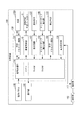
図1は、本発明に係る分光測定装置の概略構成を示すブロック図である。
分光測定装置1は、本発明の電子機器の一例であり、測定対象Xで反射した測定対象光における各波長の光強度を分析し、分光スペクトルを測定する装置である。なお、本実施形態では、測定対象Xで反射した測定対象光を測定する例を示すが、測定対象Xとして、例えば液晶パネル等の発光体を用いる場合、当該発光体から発光された光を測定対象光としてもよい。
そして、この分光測定装置1は、図1に示すように、光学モジュール10と、光学モジュール10から出力された信号を処理する制御部20と、を備えている。
[First embodiment]
Hereinafter, a first embodiment according to the present invention will be described with reference to the drawings.
[Configuration of Spectrometer]
FIG. 1 is a block diagram showing a schematic configuration of a spectrometer according to the present invention.
The spectroscopic measurement device 1 is an example of the electronic apparatus of the present invention, and is a device that analyzes the light intensity of each wavelength in the measurement target light reflected by the measurement target X and measures the spectral spectrum. In this embodiment, an example of measuring the measurement target light reflected by the measurement target X is shown. However, when a light emitter such as a liquid crystal panel is used as the measurement target X, the light emitted from the light emitter is measured. The target light may be used.
As shown in FIG. 1, the spectrometer 1 includes an
[光学モジュールの構成]
光学モジュール10は、波長可変干渉フィルター5と、ディテクター11と、I−V変換器12と、アンプ13と、A/D変換器14と、駆動制御部15とを備える。
この光学モジュール10は、測定対象Xで反射された測定対象光を、入射光学系(図示略)を通して、波長可変干渉フィルター5に導き、波長可変干渉フィルター5を透過した光をディテクター11で受光する。そして、ディテクター11から出力された検出信号は、I−V変換器12、アンプ13、及びA/D変換器14を介して制御部20に出力される。
[Configuration of optical module]
The
The
[波長可変干渉フィルターの構成]
次に、光学モジュール10に組み込まれる波長可変干渉フィルター5について説明する。
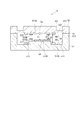
図2は、波長可変干渉フィルター5の概略構成を示す平面図である。図3は、図2におけるIII-III線を断面した際の断面図である。
波長可変干渉フィルター5は、図2及び図3に示すように、第一基板を構成する固定基板51及び第二基板を構成する可動基板52を備えている。これらの固定基板51及び可動基板52は、それぞれ例えば、ソーダガラス、結晶性ガラス、石英ガラス、鉛ガラス、カリウムガラス、ホウケイ酸ガラス、無アルカリガラス等の各種ガラスや、水晶等により形成されている。そして、固定基板51の第一接合部513及び可動基板52の第二接合部523が、例えばシロキサンを主成分とするプラズマ重合膜などにより構成された接合膜53により接合されることで、一体的に構成されている。
[Configuration of wavelength tunable interference filter]
Next, the wavelength
FIG. 2 is a plan view showing a schematic configuration of the variable
As shown in FIGS. 2 and 3, the variable
固定基板51の可動基板52に対向する面には、本発明の第一反射膜を構成する固定反射膜54が設けられ、可動基板52の固定基板51に対向する面には、本発明の第二反射膜を構成する可動反射膜55が設けられている。これらの固定反射膜54及び可動反射膜55は、ギャップG1を介して対向配置されている。そして、固定基板51及び可動基板52を厚み方向から見た平面視において、これらの固定反射膜54及び可動反射膜55が重なる領域により光干渉領域が構成される。
A fixed
波長可変干渉フィルター5には、ギャップG1のギャップ寸法を調整(変更)するのに用いられる本発明のギャップ変更部の一例である静電アクチュエーター56が設けられている。このような静電アクチュエーター56は対向する電極間に所定の電圧を印加することで、静電引力により容易にギャップG1の寸法を変化させることができ、構成の簡略化を図れる。静電アクチュエーター56は、駆動制御部15の制御により駆動可能となる。
The wavelength
また、固定基板51の可動基板52に対向する面には、第一制御電極571が設けられ、可動基板52の固定基板51に対向する面には、第二制御電極572が設けられている。これらの第一制御電極571及び第二制御電極572は対向配置されている。そして、詳細は後述するが、これらの第一制御電極571及び第二制御電極572に対して、制御電極を流すことで、反射膜54,55の傾きを制御することができる。
なお、以降の説明に当たり、固定基板51又は可動基板52の基板厚み方向から見た平面視、つまり、固定基板51及び可動基板52の積層方向から波長可変干渉フィルター5を見た平面視を、フィルター平面視と称する。また、本実施形態では、フィルター平面視において、固定反射膜54の中心点及び可動反射膜55の中心点は、一致し、平面視におけるこれらの反射膜の中心点をフィルター中心点Oと称し、これらの反射膜の中心点を通る直線を中心軸と称する。
A
In the following description, the planar view seen from the substrate thickness direction of the fixed
(固定基板の構成)
図4は、本実施形態の固定基板51を可動基板52側から見た平面図である。
固定基板51は、可動基板52に対して厚み寸法が大きく形成されており、静電アクチュエーター56による静電引力や、固定基板51上に形成される膜部材(例えば固定反射膜54等)の内部応力による固定基板51の撓みはない。
この固定基板51は、図3及び図4に示すように、例えばエッチング等により形成された電極配置溝511及び反射膜設置部512を備える。
(Configuration of fixed substrate)
FIG. 4 is a plan view of the fixed
The fixed
As shown in FIGS. 3 and 4, the fixed
電極配置溝511は、フィルター平面視で、固定基板51のフィルター中心点Oを中心とした環状に形成されている。反射膜設置部512は、フィルター平面視において、電極配置溝511の中心部から可動基板52側に突出して形成されている。この電極配置溝511の溝底面は、静電アクチュエーター56を構成する第一駆動電極561が配置される電極設置面511Aとなる。また、反射膜設置部512の突出先端面は、固定反射膜54及び第一制御電極571が配置される反射膜設置面512Aとなる。
また、固定基板51には、電極配置溝511から、固定基板51の外周縁に向かって延出する電極引出溝511Bが設けられている。具体的には、固定基板51には、固定基板51の辺C1−C2に向かって延出する電極引出溝511B1、及び辺C3−C4に向かって延出する電極引出溝511B2が設けられている。ここで、電極引出溝511B2は、固定基板51の外周縁まで延出し、電極引出溝511B1は、固定基板51の外周縁よりも所定寸法だけフィルター中心点O側の位置まで延出する。電極引出溝511B1の延出先端には電極接続部511Cが設けられ、この電極接続部511Cの可動基板52に対向する面は、第一接合部513の可動基板52に対向する面と同一平面となる。
The
The fixed
電極配置溝511の電極設置面511Aには、静電アクチュエーター56を構成する第一駆動電極561が設けられる。第一駆動電極561は、電極設置面511Aに直接設けてもよく、電極設置面511Aの上に他の薄膜(層)を設け、その上に設置してもよい。
より具体的には、第一駆動電極561は、フィルター中心点Oを中心としたC字円弧状に形成され、辺C1−C2に近接する一部にC字開口部が設けられる。また、第一駆動電極561には、第一駆動引出電極561Aが接続され、この第一駆動引出電極561Aは、電極引出溝511B1に沿って、固定基板51の外周縁まで引き出されている。つまり、第一駆動引出電極561Aは、電極引出溝511B1から、電極接続部511Cに亘って設けられている。このような第一駆動電極561及び第一駆動引出電極561Aを形成する材料としては、例えば、ITO(Indium Tin Oxide)などが挙げられる。
また、第一駆動電極561には、その表面に絶縁膜が形成されていてもよい。
A
More specifically, the
Further, an insulating film may be formed on the surface of the
反射膜設置部512は、上述したように、電極配置溝511と同軸上で、電極配置溝511よりも小さい径寸法となる略円柱状に形成され、可動基板52に対向する反射膜設置面512Aを備えている。
この反射膜設置部512には、固定反射膜54及び第一制御電極571が設置されている。
固定反射膜54は、反射膜設置部512に直接設けてもよいし、反射膜設置部512の上に他の薄膜(層)を設け、その上に設置してもよい。固定反射膜54としては、例えばAg等の金属膜や、Ag合金等、導電性の合金膜を用いることができる。Ag等の金属膜を用いる場合、Agの劣化を抑制するため保護膜を形成することが好ましい。
また、例えば高屈折率層をTiO2、低屈折率層をSiO2とし、高屈折率層と低屈折率層とを交互に積層して形成された誘電体多層膜を用いてもよく、誘電体多層膜及び金属膜を積層した反射膜や、誘電体単層膜及び合金膜を積層した反射膜等を用いてもよい。
As described above, the reflection
In the reflection
The fixed
Further, for example, a dielectric multilayer film formed by alternately stacking a high refractive index layer and a low refractive index layer using TiO 2 as a high refractive index layer and SiO 2 as a low refractive index layer may be used. A reflective film in which a multilayer film and a metal film are laminated, a reflective film in which a dielectric single layer film and an alloy film are laminated, or the like may be used.
第一制御電極571は、フィルター平面視において、固定反射膜54の外に設けられている。より具体的には、第一制御電極571は、フィルター中心点Oを中心としたC字円弧形状に形成され、辺C1−C2に近接する一部にC字開口部が設けられる。また、図4に示すように、第一制御電極571のC字開口端の一方(頂点C1側)には、入力用の第一制御引出電極571A1が接続され、第一制御電極571のC字開口端の他方(頂点C2側)には、出力用の第一制御引出電極571A2が接続される。
これらの第一制御引出電極571A(571A1,571A2)は、電極引出溝511B1に沿って、固定基板51の外周縁まで引き出されている。つまり、第一制御引出電極571Aは、電極引出溝511B1から、電極接続部511Cに亘って設けられている。
このような第一制御電極571及び第一制御引出電極571Aを形成する材料としては、第一駆動電極561や第一駆動引出電極561Aと同じ材料を用いることができ、例えば、ITO(Indium Tin Oxide)などを用いることができる。
また、第一制御電極571の表面には、絶縁膜571Bが成膜されている。
The
These first
As a material for forming the
An insulating
さらに、固定基板51の光入射面(固定反射膜54が設けられない面)には、固定反射膜54に対応する位置に反射防止膜を形成してもよい。この反射防止膜は、低屈折率膜及び高屈折率膜を交互に積層することで形成することができ、固定基板51の表面での可視光の反射率を低下させ、透過率を増大させる。
Furthermore, an antireflection film may be formed at a position corresponding to the fixed
(可動基板の構成)
図5は、本実施形態の波長可変干渉フィルターにおける可動基板52を固定基板51側から見た平面図である。
可動基板52は、図2及び図4に示すように、フィルター平面視においてフィルター中心点Oを中心とした円形状の可動部521と、可動部521と同軸であり可動部521を保持する保持部522と、保持部522の外側に設けられた第二接合部523と、第二接合部523の外側に設けられた端子部524と、を備えている。
(Configuration of movable substrate)
FIG. 5 is a plan view of the
As shown in FIGS. 2 and 4, the
可動部521は、保持部522よりも厚み寸法が大きく形成され、例えば、本実施形態では、可動基板52(第二接合部523や端子部524)の厚み寸法と同一寸法に形成されている。この可動部521は、フィルター平面視において、少なくとも反射膜設置面512Aの外周縁の径寸法よりも大きい径寸法に形成されている。そして、この可動部521には、静電アクチュエーター56を構成する第二駆動電極562、可動反射膜55、及び第二制御電極572が設けられている。第二駆動電極562、可動反射膜55、及び第二制御電極572は、可動面521Aに直接設けてもよいし、可動面521Aの上に他の薄膜(層)を設け、その上に設置してもよい。
なお、固定基板51と同様に、可動部521の固定基板51とは反対側の面には、反射防止膜が形成されていてもよい。
The
Similar to the fixed
第二駆動電極562は、フィルター中心点Oを中心としたC字円弧状に形成され、固定基板51の辺C3−C4に対応した辺C3´−C4´に近接する一部にC字開口部が設けられている。また、第二駆動電極562には、第二駆動引出電極562Aが接続され、この第二駆動引出電極562Aは、電極引出溝511B2に対向する領域に沿って、可動基板52の外周縁まで引き出されている。つまり、第二駆動引出電極562Aは、可動部521から端子部524に亘って設けられている。このような第二駆動電極562及び第二駆動引出電極562Aを形成する材料としては、例えば、ITOなどが挙げられる。そして、第二駆動引出電極562Aは、端子部524において、例えばFPCやリード線等により、駆動制御部15に接続されている。
また、第二駆動電極562には、その表面に絶縁膜が形成されていてもよい。
The
The
本実施形態では、図2に示すように、第一駆動電極561と第二駆動電極562とが重なる領域(図2の右下がりハッチで示す領域)により静電アクチュエーター56が構成される。これにより、静電アクチュエーター56は、フィルター中心点Oに対して、点対称となる領域に静電引力を発生させることができるため、可動部521の傾斜を抑制してバランスよく可動部521を固定基板51側に変位させることが可能となる。
In the present embodiment, as shown in FIG. 2, the
可動反射膜55は、可動部521の可動面521Aの中心部に、固定反射膜54とギャップG1を介して対向して設けられる。この可動反射膜55としては、上述した固定反射膜54と同一の構成の反射膜が用いられる。
なお、本実施形態では、駆動電極561,562間のギャップG2が反射膜54,55間のギャップG1よりも大きい例を示すがこれに限定されない。例えば、測定対象光として赤外線や遠赤外線を用いる場合等、測定対象光の波長域によっては、ギャップG1がギャップG2よりも大きくなる構成としてもよい。
The movable
In this embodiment, an example in which the gap G2 between the
第二制御電極572は、フィルター平面視において、可動反射膜55の外で、第二駆動電極562よりフィルター中心点O側に設けられ、第一制御電極571と対向する。より具体的には、第二制御電極572は、フィルター中心点Oを中心としたC字円弧形状に形成され、辺C3´−C4´に近接する一部にC字開口部が設けられる。また、図5に示すように、第二制御電極572のC字開口端部の一方(頂点C4´側)には、入力用の第二制御引出電極572A1が接続され、C字開口端部の他方(頂点C3´側)には、出力用の第二制御引出電極572A2が接続されている。これらの第二制御引出電極572A(572A1,572A2)は、電極引出溝511B2に沿って、可動基板52の外周縁まで引き出されている。つまり、第二制御引出電極572Aは、可動部521から端子部524に亘って設けられている。そして、第二制御引出電極572Aは、端子部524において、例えばFPCやリード線等により、駆動制御部15に接続されている。
このような第二制御電極572及び第二制御引出電極572Aを形成する材料としては、第二駆動電極562や第二駆動引出電極562Aと同じ材料を用いることができ、例えば、ITOなどを用いることができる。
また、第二制御電極572の表面には、絶縁膜572Bが成膜されている。
The
As a material for forming the
An insulating
ここで、第一制御電極571上の絶縁膜571Bと、第二制御電極572の絶縁膜572Bとの間のギャップG3は、反射膜54,55間のギャップG1よりも小さい。具体的には、反射膜54,55として、制御電極571,572の厚み寸法を、反射膜54,55の厚み寸法より大きくする。また、第一制御電極571及び絶縁膜571Bの厚み寸法の合計、及び第二制御電極572及び絶縁膜572Bの厚み寸法の合計を、それぞれ反射膜54,55の厚み寸法より大きくしてもよい。
また、反射膜54,55として誘電体多層膜等の積層膜を用いる場合では、反射膜設置部512のうち、第一制御電極571の設置位置を反射膜設置面512Aよりも可動基板52側に突出させる構成としてもよい。
このように、ギャップG3をギャップG1よりも小さくすることで、反射膜54,55同士の接触を防止することができる。
Here, the gap G3 between the insulating
Further, in the case of using a laminated film such as a dielectric multilayer film as the
Thus, by making the gap G3 smaller than the gap G1, the contact between the
保持部522は、可動部521の周囲を囲うダイヤフラムであり、可動部521よりも厚み寸法が小さく形成されている。このような保持部522は、可動部521よりも撓みやすく、僅かな静電引力により、可動部521を固定基板51側に変位させることが可能となる。この際、可動部521が保持部522よりも厚み寸法が大きく、剛性が大きくなるため、可動部521が静電引力により固定基板51側に引っ張られた場合でも、可動部521の形状変化をある程度抑制出来る。
なお、本実施形態では、ダイヤフラム状の保持部522を例示するが、これに限定されず、例えば、可動部521のフィルター中心点Oを中心として、等角度間隔で配置された梁状の保持部が設けられる構成などとしてもよい。
The holding
In the present embodiment, the diaphragm-
端子部524は、第二接合部523の外側に設けられている。具体的には、端子部524は、固定基板51の辺C1−C2から外側に突出する端子部524Aと、固定基板51の辺C3−C4から外側に突出する端子部524Bとを備えている。
そして、可動基板52には、第二接合部523のうち固定基板51の電極接続部511Cに対向する領域から、端子部524Aに亘って、3つの接続電極563,573A,573Bが設けられている。固定基板51及び可動基板52が接合された状態で、接続電極563は、第一駆動引出電極561Aに接続され、接続電極573Aは第一制御引出電極571A1に接続され、接続電極573Bは第一制御引出電極571A2に接続される。そして、これらの接続電極563,573A,573Bは、端子部524において、例えばFPCやリード線等により、駆動制御部15に接続されている。
The
The
[光学モジュールの検出部、I−V変換器、アンプ、A/D変換器の構成]
次に、図1に戻り、光学モジュール10について説明する。
ディテクター11は、波長可変干渉フィルター5を透過した光を受光(検出)し、受光量に基づいた検出信号をI−V変換器12に出力する。
I−V変換器12は、ディテクター11から入力された検出信号を電圧値に変換し、アンプ13に出力する。
アンプ13は、I−V変換器12から入力された検出信号に応じた電圧(検出電圧)を増幅する。
A/D変換器14は、アンプ13から入力された検出電圧(アナログ信号)をデジタル信号に変換し、制御部20に出力する。
[Configuration of optical module detector, IV converter, amplifier, A / D converter]
Next, returning to FIG. 1, the
The
The
The
The A /
[駆動制御部の構成]
駆動制御部15は、図1に示すように、静電アクチュエーター56に印加する駆動電圧を制御する電圧制御部151と、第一制御電極571及び第二制御電極572に流す制御電流を制御する傾斜制御部152と、を備えている。
電圧制御部151は、制御部20の制御に基づいて、波長可変干渉フィルター5の静電アクチュエーター56に対して駆動電圧を印加する。これにより、静電アクチュエーター56の第一駆動電極561及び第二駆動電極562間で静電引力が発生し、可動部521が固定基板51側に変位する。
[Configuration of drive control unit]
As shown in FIG. 1, the
The
傾斜制御部152は、第一制御電極571に、第一制御引出電極571A1から第一制御引出電極571A2に向かう第一方向に沿って第一制御電流を流す。また、傾斜制御部152は、第二制御電極572に、第二制御引出電極572A1から第二制御引出電極572A2に向かう第二方向に沿って第二制御電流を流す。つまり、図2に示すようなフィルター平面視において、第一制御電極571には、反時計回りに第一制御電流が流れ、第二制御電極572には、時計回りに第二制御電流が流れる。
これにより、第一制御電極571及び第二制御電極572が対向する領域(図2における右上がりハッチで示す領域)には、ローレンツ力による斥力が発生する。
The
As a result, a repulsive force due to the Lorentz force is generated in a region where the
図6及び図7は、制御電極571,572に電流を流した際に発生するローレンツ力を示す図である。
微小電極要素dlに作用するローレンツ力をFr、第一制御電流をI1、第二制御電流をI2、真空中の透磁率をμ0、制御電極571,572間のギャップG3のギャップ寸法をr、第一制御電極571の曲率半径をR1、第二制御電極572の曲率半径をR2とする。
曲率半径R1,R2>>ギャップ寸法rとなる場合、微小電極要素dlに作用するローレンツ力Frは、2本の平行電流間に作用するローレンツ力と同じとみなせる。実際、ギャップ寸法rは、数100nm程度に対して、曲率半径は、数mmのため、曲率半径R1,R2>>ギャップ寸法rの関係は成り立つ。2本の平行電流間に作用するローレンる力は一般に下記式(1)により表せる。
6 and 7 are diagrams showing the Lorentz force generated when a current is passed through the
The Lorentz force acting on the microelectrode element dl is F r , the first control current is I 1 , the second control current is I 2 , the magnetic permeability in vacuum is μ 0 , and the gap size of the gap G3 between the
When the curvature radii R1, R2 >> gap dimension r, the Lorentz force F r acting on the microelectrode element dl can be regarded as the same as the Lorentz force acting between the two parallel currents. Actually, the gap dimension r is about several hundred nm, and the radius of curvature is several mm. Therefore, the relationship of the curvature radii R1, R2 >> gap dimension r is established. The Lauren force acting between two parallel currents can be generally expressed by the following formula (1).
Fr=(μ0I1I2/2πr)dl …(1) F r = (μ 0 I 1 I 2 / 2πr) dl (1)
式(1)に示すように、制御電極571,572間のギャップG3のギャップ寸法が小さくなるほど、ローレンツ力による斥力が大きくなる。これにより、図6に示すように、可動部521に傾斜がある場合、ギャップG3のギャップ寸法が均等になるように、ローレンツ力が作用することになる。また、図7に示すように、可動部521の傾斜がなく、反射膜54,55が平行である場合は、均等な斥力が作用することになり、反射膜54,55の平行度を維持する。
As shown in Expression (1), the repulsive force due to the Lorentz force increases as the gap dimension of the gap G3 between the
図8は、波長可変干渉フィルター5から各波長の光を取り出す際に、制御電極571,572間に作用させる斥力(ローレンツ力)、及び静電アクチュエーター56に作用させる静電引力の一例を示す図である。
図8に示すように、駆動制御部15は、制御電極571,572間に作用させる斥力が、駆動電極561,562間に作用せる静電引力と略同一、若しくは静電引力より小さくなるように、駆動電圧及び制御電流を設定する。
図8では、制御電流として0.2A、0.1A,0.05A、0.01Aを例示するが、これらの値のうちいずれか1つにより制御電極571,572間の斥力を制御すればよい。なお、波長可変干渉フィルター5を透過させる光の波長によって、制御電極571,572に流す制御電流を切り替えてもよい。例えば、ギャップG3の寸法が大きいと斥力が小さくなるので、所定波長(例えば500nm)以上の光を透過させる場合に、例えば0.1Aの制御電流を選択し、前記所定波長未満の光を透過させる場合に、例えば、0.05Aの制御電流を選択するなどの制御を行ってもよい。
さらに、第一制御電流I1及び第二制御電流I2としては、異なる電流値としてもよい。上記式(1)に示すように、これらの制御電流I1,I2を適宜設定することで、制御電極571,572間に作用するローレンツ力をより細かく設定することができる。
FIG. 8 is a diagram illustrating an example of a repulsive force (Lorentz force) that acts between the
As shown in FIG. 8, the
In FIG. 8, 0.2 A, 0.1 A, 0.05 A, and 0.01 A are exemplified as the control current, but the repulsive force between the
Further, the first control current I 1 and the second control current I 2 may have different current values. As shown in the above formula (1), the Lorentz force acting between the
[制御部の構成]
次に、分光測定装置1の制御部20について説明する。
制御部20は、例えばCPUやメモリー等が組み合わされることで構成され、分光測定装置1の全体動作を制御する。この制御部20は、図1に示すように、波長設定部21と、光量取得部22と、分光測定部23と、を備えている。また、制御部20のメモリーには、波長可変干渉フィルター5を透過させる光の波長と、当該波長に対応して静電アクチュエーター56に印加する駆動電圧との関係を示すV−λデータが記憶されている。
なお、本実施形態では、制御電極571,572に制御電流を流した際にローレンツ力による斥力が発生する。したがって、この斥力を考慮して反射膜54,55間のギャップG1の寸法を所定波長に対応した寸法に設定可能な駆動電圧が記憶される。
[Configuration of control unit]
Next, the
The
In the present embodiment, repulsive force due to Lorentz force is generated when a control current is passed through the
波長設定部21は、波長可変干渉フィルター5により取り出す光の目的波長を設定し、V−λデータに基づいて、設定した目的波長に対応する駆動電圧を静電アクチュエーター56に印加させる旨の指令信号を駆動制御部15に出力する。
光量取得部22は、ディテクター11により取得された光量に基づいて、波長可変干渉フィルター5を透過した目的波長の光の光量を取得する。
分光測定部23は、光量取得部22により取得された光量に基づいて、測定対象光のスペクトル特性を測定する。
The
The light
The
[駆動制御部による波長可変干渉フィルターの駆動処理]
次に、上述のような駆動制御部15により、波長可変干渉フィルター5を駆動させる際の処理について説明する。
駆動制御部15は、制御部20の波長設定部21からの指令信号に基づいて、波長可変干渉フィルター5を駆動させる。
具体的には、電圧制御部151により、指令信号に応じた駆動電圧を波長可変干渉フィルター5の静電アクチュエーター56に印加すると同時に、傾斜制御部152は、予め設定された第一制御電流を第一制御電極571に印加し、第二制御電流を第二制御電極572に流す。
これにより、制御電極571,572により発生するローレンツ力の斥力により、可動部521の傾斜が抑制され、反射膜54,55の平行度を維持した状態で、ギャップG1のギャップ寸法を、目標値に設定することが可能となる。
[Drive processing of variable wavelength interference filter by drive control unit]
Next, processing when the wavelength
The
Specifically, the
As a result, the repulsive force of the Lorentz force generated by the
この際、傾斜制御部152は、可動部521の変位(振動)が収束するまでの時間(安定化時間)、各制御電極571,572に制御電流を流し続ける。このような制御を行うことで、安定化時間の短縮を図ることができる。つまり、静電アクチュエーター56に駆動電圧を印加して可動部521を撓ませると、可動基板52(保持部522)のばね力に応じて、可動部521が振動するが、制御電極571,572により、静電引力に抗する斥力が作用するため、可動部521の振動速度を低減でき、安定化時間の短縮を図ることができる。
At this time, the
[第一実施形態の作用効果]
本実施形態では、波長可変干渉フィルター5は、固定基板51に設けられた第一制御電極571と、可動基板52に設けられた第二制御電極572とを備え、傾斜制御部152は、第一制御電極571に、第一制御電流を流し、第二制御電極572に、フィルター平面視において、第一制御電流と逆方向となる第二制御電流を流す。
このため、第二制御電極572には、固定基板51から離れる方向にローレンツ力(斥力)が作用し、当該ローレンツ力は、制御電極571,572間のギャップG3のギャップ寸法が小さいほど大きい力となる。したがって、このようなローレンツ力により、可動部521の傾斜を抑制することができ、反射膜54,55の平行度の悪化を抑制することができる。これにより、波長可変干渉フィルター5から高分解能で目的波長の光を透過させることができる。よって、光学モジュール10において、目的波長の光の正確な光量を検出することができ、分光測定装置1において、各波長の正確な光量に基づいて精度の高い分光測定処理を実施することができる。
[Operational effects of the first embodiment]
In the present embodiment, the wavelength
Therefore, a Lorentz force (repulsive force) acts on the
本実施形態では、電圧制御部151により静電アクチュエーター56に電圧を印加させることで、反射膜54,55間のギャップG1の寸法を所望の値に設定することができる。
ここで、静電アクチュエーター56に駆動電圧を印加する際に、可動部521には静電引力と可動基板52が有するばね力とにより、可動部521が振動する。これに対して、本実施形態では、傾斜制御部152は、可動部521の振動が収束するまでの間、制御電極571,572に制御電流を流し続ける。このため、静電引力に対して抗する斥力により、可動部521の振動を静止させる方向に力が作用し、可動部521の振動収束までの安定化時間を短縮することができる。
したがって、より迅速な光量取得が可能となり、分光測定処理に係る時間も短縮することができる。
In the present embodiment, by applying a voltage to the
Here, when a drive voltage is applied to the
Therefore, it is possible to acquire the light amount more quickly and to shorten the time for the spectroscopic measurement process.
本実施形態では、制御電極571,572間のギャップG3が、反射膜54,55間のギャップG1よりも小さい。このため、反射膜54,55間のギャップG1の寸法を小さくする際に、制御電極571,572が当接することで、反射膜54,55同士の接触を防止でき、接触による反射膜54,55の劣化を抑制できる。
また、制御電極571,572の表面に絶縁膜571B,572Bが設けられているので、上述のように制御電極571,572同士が接触した場合でも、短絡を防止できる。
In the present embodiment, the gap G3 between the
In addition, since the insulating
[第一実施形態の変形例]
上述した第一実施形態では、第一制御電極571がフィルター平面視において固定反射膜54の外に設けられ、第二制御電極572が可動反射膜55の外に設けられる構成例を示した。
これに対して、フィルター平面視において、第一制御電極571が固定反射膜54に重なる領域に設けられ、第二制御電極572が可動反射膜55に重なる領域に設けられる構成としてもよい。
図9は、第一実施形態の一変形例における波長可変干渉フィルターにおける固定基板51を可動基板52側から見た平面図である。なお、可動反射膜55及び第二制御電極572の位置関係についての図示は省略する。
図9に示すように、第一制御電極571が設けられる位置としては、固定反射膜54上であってもよい。この場合、固定反射膜54が例えば誘電体多層膜等の非導電性素材により構成されている場合、第一制御電極571を直接固定反射膜54上に設けてもよい。また、固定反射膜54が金属膜等の導電性素材により構成されている場合、絶縁膜を介して第一制御電極571を設ければよい。
また、第二制御電極572においても同様に、可動反射膜55上に設けられ、第一制御電極571及び第二制御電極572がフィルター平面視において重なる位置に配置される。
[Modification of First Embodiment]
In the first embodiment described above, the configuration example in which the
On the other hand, the
FIG. 9 is a plan view of the fixed
As shown in FIG. 9, the position where the
Similarly, the
上述のように、反射膜54,55上に制御電極571,572を設ける構成では、制御電極571,572に制御電流を流すことで、反射膜54,55に対して直接ローレンツ力による斥力を作用させることができ、反射膜54,55の平行度をより精度よく制御することができる。また、図4及び図9を比較すると分かるように、反射膜54,55の設置面積を大きくでき、波長可変干渉フィルター5を透過する光の光量を増大させることができる。
As described above, in the configuration in which the
[第二実施形態]
次に、本発明に係る第二実施形態について、図面に基づいて説明する。
上述した第一実施形態では、固定基板51に設けられた第一制御電極571と、可動基板52に設けられた第二制御電極572とに、それぞれ、フィルター平面視において逆方向となる制御電流を流す例を示した。これに対して、第二実施形態では、第一制御電極571及び第二制御電極572が設けられず、反射膜54,55に制御電流を流す点で、上記第一実施形態と相違する。
なお、以降の実施形態の説明にあたり、上述した第一実施形態と同様の構成については同符号を付し、その説明を省略、または簡略化する。
[Second Embodiment]
Next, 2nd embodiment which concerns on this invention is described based on drawing.
In the first embodiment described above, the control currents in the opposite directions in the filter plan view are respectively applied to the
In the following description of the embodiments, the same reference numerals are given to the same configurations as those of the first embodiment described above, and the description thereof is omitted or simplified.
図10は、本発明に係る第二実施形態の波長可変干渉フィルターにおける、固定反射膜及び可動反射膜の概略構成、及びこれらの反射膜に流れる制御電流を示す図である。
本実施形態では、固定反射膜54及び可動反射膜55として、例えば金属膜や金属合金膜等の導電性の反射膜が用いられる。また、誘電体多層膜の表層に透過性を有する導電性膜を形成する構成などとしてもよい。
そして、本実施形態では、図10に示すように、固定反射膜54には、入力用の固定引出電極54Aと、出力用の固定引出電極54Bとが接続され、これらの入力用の固定引出電極54A及び出力用の固定引出電極54Bは、それぞれ、固定反射膜54の外周縁のうちフィルター中心点Oに対して点対称となる位置に接続されている。
また、可動反射膜55には、入力用の可動引出電極55Aと、出力用の可動引出電極55Bとが接続され、これらの入力用の可動引出電極55A及び出力用の可動引出電極55Bは、それぞれ、可動反射膜55の外周縁のうちフィルター中心点Oに対して点対称となる位置に接続されている。
また、これらの引出電極54A,54B,55A,55Bは、それぞれ傾斜制御部152に接続されている。
また、本実施形態の波長可変干渉フィルターにおいても、第一実施形態と同様に、ギャップ変更部である静電アクチュエーター56が設けられている。
FIG. 10 is a diagram showing a schematic configuration of the fixed reflection film and the movable reflection film and a control current flowing through these reflection films in the variable wavelength interference filter according to the second embodiment of the present invention.
In the present embodiment, as the fixed
In this embodiment, as shown in FIG. 10, the fixed
The movable
Further, these
Also in the variable wavelength interference filter of the present embodiment, an
そして、傾斜制御部152は、図10に示すように、入力用の固定引出電極54Aから出力用の固定引出電極54Bに向かって第一制御電極を流し、入力用の可動引出電極55Aから出力用の可動引出電極55Bに向かって第二制御電極を流す。これにより、上述した第一実施形態と同様に、フィルター平面視において、固定反射膜54及び可動反射膜55に流れる制御電流の方向が、互いに逆方向となり、固定反射膜54及び可動反射膜55間にローレンツ力による斥力が発生する。
また、本実施形態の傾斜制御部152においても、第一実施形態と同様に、静電アクチュエーター56によりギャップG1のギャップ寸法を変化させた際に、第二基板の振動が収束する安定化時間までの間、傾斜制御部152は、制御電流を流し続ける。これにより、安定化時間の短縮を図ることができる。
Then, as shown in FIG. 10, the
Further, in the
[第二実施形態の作用効果]
本実施形態では、傾斜制御部152は、固定反射膜54に第一制御電流を流し、可動反射膜55に、フィルター平面視において第一制御電流と逆方向となる第二制御電流を流す。
このため、可動反射膜55には、ローレンツ力による斥力が作用し、当該ローレンツ力は、反射膜54,55間のギャップG1のギャップ寸法が小さいほど大きい力となる。このため、第一実施形態と同様に、可動部521の傾斜を抑制することができ、反射膜54,55の平行度の悪化を抑制することができる。
また、本実施形態では、可動反射膜55に対して直接ローレンツ力が作用する。このため、固定反射膜54及び可動反射膜55の互いに対向する領域内において、例えば、可動反射膜55の中心部が固定基板51側に撓んでいる場合等でも、その撓みを修正して反射膜54,55が平行となるように作用させることができる。したがって、より確実に反射膜54,55の平行度を維持することができ、波長可変干渉フィルター5の分解能低下を抑制できる。
[Operational effects of the second embodiment]
In the present embodiment, the
Therefore, a repulsive force due to the Lorentz force acts on the movable
In the present embodiment, the Lorentz force acts directly on the movable
[第二実施形態の変形例]
上述した第二実施形態では、固定反射膜54及び可動反射膜55がそれぞれ1つのみ設けられる構成例を示した。これに対して、複数の固定反射膜54と、これに対向する複数の可動反射膜55とを備える構成にも適用できる。
図11は、第二実施形態の変形例における波長可変干渉フィルター5Aの概略構成を示す断面図である。図12は、第二実施形態の変形例の波長可変干渉フィルター5Aの固定反射膜54の接続構成を示す図である。図13は、第二実施形態の変形例の波長可変干渉フィルター5Aの可動反射膜55の接続構成を示す図である。
[Modification of Second Embodiment]
In the second embodiment described above, the configuration example in which only one fixed
FIG. 11 is a cross-sectional view illustrating a schematic configuration of a variable
この波長可変干渉フィルター5Aでは、図11に示すように、光干渉領域58内に、複数の固定反射膜54及び可動反射膜55が設けられている。そして、一対の固定反射膜54及び可動反射膜55により1つの光干渉部581が構成され、各光干渉部581に対してそれぞれ独立したディテクター11が設けられている。このような波長可変干渉フィルター5Aでは、各光干渉部581を透過した光をディテクター11により受光させることが可能となる。
また、図示は省略するが、各反射膜54,55間のギャップG1の寸法を変更するための静電アクチュエーター56が、フィルター平面視において光干渉領域58の外に設けられている。
In the variable
Although not shown, an
そして、複数の固定反射膜54は、図12に示すように直列に接続され、直列に接続された固定反射膜54のうち一端部に接続された固定反射膜541には、入力用の固定引出電極54Aが接続されている。また、直列に接続された固定反射膜54のうち他端部に接続された固定反射膜542には、出力用の固定引出電極54Bが接続されている。
同様に、複数の可動反射膜55は、図13に示すように直列に接続され、直列に接続された可動反射膜55のうち固定反射膜541に対向する可動反射膜551には、出力用の可動引出電極55Bが接続されている。また、直列に接続された可動反射膜55のうち固定反射膜542に対向する可動反射膜552には、入力用の可動引出電極55Aが接続されている。
これらの引出電極54A,54B,55A,55Bは、第二実施形態と同様、それぞれ傾斜制御部152に接続されている。
The plurality of fixed
Similarly, the plurality of movable
These
そして、傾斜制御部152は、第二実施形態と同様に、入力用の固定引出電極54Aから出力用の固定引出電極54Bに向かって第一制御電極を流し、入力用の可動引出電極55Aから出力用の可動引出電極55Bに向かって第二制御電極を流す。
このような波長可変干渉フィルター5Aでは、各光干渉部581における反射膜54,55間のギャップG1の寸法に応じたローレンツ力を作用させることができる。したがって、各光干渉部581におけるギャップG1の寸法を一様に維持することができ、各光干渉部581を透過する光の波長を高精度に揃えることができる。
Then, as in the second embodiment, the
In such a wavelength
なお、上記図11から図13の例では、反射膜54,55を円形状に構成する例を示したが、例えば図14に示すように、固定反射膜54とこれらを接続する電極とを同一幅寸法に構成してもよい。可動反射膜55においても同様である。
11 to 13 show an example in which the
さらに、上記図11から図14の例において、個々の光干渉部581に対してそれぞれ静電アクチュエーター56が設けられ、各光干渉部581を透過する光の波長をそれぞれ個別に設定可能な構成としてもよい。この場合でも、各光干渉部581において、第二実施形態と同様に、反射膜54,55の平行度を高精度に維持することができ、各光干渉部581の分解能を向上することができる。
Furthermore, in the examples of FIGS. 11 to 14, the
[第三実施形態]
次に、本発明に係る第三実施形態について、図面に基づいて説明する。
上述した第一及び第二実施形態では、傾斜制御部152は、可動部521の振動が収束するまでの間、制御電極571,572(第二実施形態では、反射膜54,55)に制御電流を流し続けることで、安定化時間の短縮を図った。これに対して、第三実施形態では、傾斜制御部152Aは、制御電極571,572に制御電流を流すことで、ローレンツ力の斥力により可動部521の傾斜を抑制するとともに、フィードバック制御時に当該ローレンツ力による斥力を駆動用の動力としても利用する。
[Third embodiment]
Next, a third embodiment according to the present invention will be described based on the drawings.
In the first and second embodiments described above, the
図15は、第三実施形態の光学モジュール10Aの概略構成を示す図である。
本実施形態の波長可変干渉フィルター5Bでは、反射膜54,55が導電性を有し、これらの反射膜54,55を静電容量検出用電極として機能させる。つまり、反射膜54,55には、それぞれ静電容量検出用引出電極(図示略)が接続されており、駆動制御部15Aのギャップ検出部153に接続されている。このような静電容量検出用引出電極としては、例えば固定反射膜54に対して、図4における入力用の第一制御電極571A1と、出力用の第一制御電極571A2との間に配置することができ、可動反射膜55に対して、図5における入力用の第二制御電極572A1と、出力用の第二制御電極572A2との間に配置することができる。
なお、本実施形態では、反射膜54,55を静電容量検出用の電極としても機能させるが、例えば第二実施形態のように、反射膜54,55に制御電流を流す構成等では、別途、静電容量検出用の電極を固定基板51及び可動基板52に設ける構成としてもよい。
FIG. 15 is a diagram illustrating a schematic configuration of an
In the wavelength
In the present embodiment, the
一方、図15に示すように、光学モジュール10Aを構成する駆動制御部15Aは、電圧制御部151と、傾斜制御部152Aと、ギャップ検出部153と、フィードバック制御部154とを備えている。
ギャップ検出部153は、反射膜54,55における静電容量を検出し、検出信号をフィードバック制御部154に出力する。
フィードバック制御部154は、傾斜制御部152Aにフィードバック信号を出力する。
傾斜制御部152Aは、制御電極571,572に対して、制御電流を流して、可動部521の傾斜を抑制するとともに、フィードバック信号に基づいて、制御電流の電流値を増減させる。
On the other hand, as illustrated in FIG. 15, the
The
The
The
上述したような構成では、以下のように、波長可変干渉フィルター5Bの動作を制御する。
駆動制御部15Aは、制御部20から指令信号が入力されると、電圧制御部151は、指令信号に応じた駆動電圧を静電アクチュエーター56に印加する。なお、本実施形態では、電圧制御部151は、ギャップG1の寸法が、目標波長に対応した寸法よりも小さくなるように駆動電圧を印加する。
この際、傾斜制御部152Aは、第一実施形態と同様に、制御電極571,572に対して制御電流を流して、可動部521の傾斜を抑制する。
In the configuration as described above, the operation of the wavelength
When a command signal is input from the
At this time, the
一方、ギャップ検出部153は、反射膜54,55に対して、静電容量検出用高周波電圧を印加し、反射膜54,55に保持された静電容量を検出する。
また、ギャップ検出部153は、検出した静電容量に応じた検出信号をフィードバック制御部154に出力する。
フィードバック制御部154は、検出信号が入力されると、制御部20から入力された指令信号との偏差を算出し、偏差に応じたフィードバック信号を傾斜制御部152Aに出力する。
On the other hand, the
Further, the
When the detection signal is input, the
傾斜制御部152Aは、フィードバック制御部154からフィードバック信号が入力されると、フィードバック信号に基づいて、第一制御電極571に流す第一制御電流、及び第二制御電極572に流す第二制御電流の少なくともいずれかの電流値を増減させて、第二制御電極572に作用させるローレンツ力(斥力)の強さを増減させる。
以上のようなフィードバック制御を、フィードバック制御部154で算出される偏差が0(若しくは予め設定された閾値以下)となるまで実施し、ギャップG1のギャップ寸法を目的波長に対応した寸法に設定する。
When a feedback signal is input from the
The feedback control as described above is performed until the deviation calculated by the
[第三実施形態の作用効果]
本実施形態では、傾斜制御部152Aは、制御電極571,572に流す制御電流をフィードバック信号に応じて増減させる。これにより、可動部521の傾斜をローレンツ力による斥力で抑制させつつ、当該ローレンツ力の大きさを変更することで、ギャップG1の寸法制御を行うことができる。
ここで、ローレンツ力は、上述した式(1)に示すように、制御電極571,572間のギャップG3のギャップ寸法dの−1乗に比例する。一方、静電アクチュエーター56に作用する静電引力は、駆動電極561,562間のギャップG2のギャップ寸法の−2乗に比例する。したがって、ローレンツ力の制御は、静電引力の制御に比べて感度が低く、ギャップG3が小さい場合でも、高精度な制御が可能となる。
これにより、波長可変干渉フィルター5から精度よく目的波長の光を透過させることができる。また、上述した第一実施形態と同様に、静電引力に抗するローレンツ力を作用させることで、可動部521の振動を抑制でき、安定化時間の短縮をも図ることができ、可動部521の傾斜を抑制できるため、分解能が高い(半値幅が小さい)光を透過させることができる。
[Operational effects of the third embodiment]
In the present embodiment, the
Here, the Lorentz force is proportional to the negative power of the gap dimension d of the gap G3 between the
Thereby, the light of the target wavelength can be accurately transmitted from the wavelength
[その他の実施形態]
なお、本発明は前述の実施形態に限定されるものではなく、本発明の目的を達成できる範囲での変形、改良等は本発明に含まれるものである。
例えば、第一実施形態において、略C字円弧状の制御電極571,572を構成する例を示したが、これに限定されない。
図16、図17、及び図18は、第一制御電極571の他の形状例を示す図である。なお、第二制御電極572においても同様であるため、ここでの図示は省略する。
図16に示すように、複数の第一制御電極571が設けられ、各第一制御電極571の端部にそれぞれ第一制御引出電極571A1,571A2が設けられる構成としてもよい。図16では、複数の第一制御電極571に対して、共通の第一制御引出電極571A1,571A2を用いる例を示す。この場合、各第一制御電極571の電気抵抗が同じである場合、同一電流値の第一制御電流が流れる。なお、各第一制御電極571に対して、それぞれ独立した第一制御引出電極571A1,571A2を設ける構成としてもよい。この場合、各第一制御電極571に対して異なる第一制御電流を流すこともできる。
図17に示す例は、第一制御電極571が、複数の円弧部571C1と、これらの円弧部571C1を接続する接続部571C2とにより構成される。
上記のような図16及び図17のような電極パターンでは、ローレンツ力による斥力を発生させる領域が増大するため、より大きい斥力により可動部521の傾斜を抑制することができる。
[Other Embodiments]
It should be noted that the present invention is not limited to the above-described embodiments, and modifications, improvements, and the like within the scope that can achieve the object of the present invention are included in the present invention.
For example, in the first embodiment, an example in which the
16, FIG. 17, and FIG. 18 are diagrams showing other shape examples of the
As shown in FIG. 16, a plurality of
In the example shown in FIG. 17, the
In the electrode pattern as shown in FIGS. 16 and 17 as described above, the region where the repulsive force is generated due to the Lorentz force is increased, so that the tilt of the
また、図18に示すように、第一制御電極571を2つ以上の電極に分割する構成としてもよい。図18は、2つの第一制御電極571D,571Eに分割し、これらに対向する第二制御電極572も同様に2つの第二制御電極572D,572Eに分割した例である。
図18に示す例では、傾斜制御部152は、第一制御電極571Dに、第一制御引出電極571D1から第一制御引出電極571D2に向かう方向で第一制御電流を流し、第一制御電極571Eに、第一制御引出電極571E1から第一制御引出電極571E2に向かう方向で第一制御電極571Dに対する第一制御電流と同じ大きさの第一制御電流を流す。また、傾斜制御部152は、第二制御電極572Dに、第二制御引出電極572D1から第二制御引出電極572D2に向かう方向に第二制御電流を流し、第二制御電極572Eに、第二制御引出電極572E1から第二制御引出電極572E2に向かう方向に第二制御電極572Dに対する第二制御電流と同じ大きさの第二制御電流を流す。
なお、傾斜制御部152は、第一制御電極571Dに、第一制御引出電極571D1から第一制御引出電極571D2に向かう方向に第一制御電流を流し、第一制御電極571Eに、第一制御引出電極571E2から第一制御引出電極571E1に向かう方向に第一制御電流を流してもよい。この場合、傾斜制御部152は、第二制御電極572Dに、第二制御引出電極572D1から第二制御引出電極572D2に向かう方向に第二制御電流を流し、第二制御電極572Eに、第二制御引出電極572E2から第二制御引出電極572E1に向かう方向に第二制御電流を流す。
なお、第一制御電極571D及び第一制御電極571Eに対して同一の電流値の第一制御電流を流す例を示すが、例えば、可動部521の傾斜量等に応じて、これらの第一制御電流の電流値を異なる値に設定することもできる。第二制御電極572D,572Eに対する第二制御電流についても同様である。
Further, as shown in FIG. 18, the
In the example illustrated in FIG. 18, the
The
In addition, although the example which sends the 1st control current of the same electric current value with respect to
また、図16及び図18に示す例では、第二制御電極572を、第一制御電極571と同一形状に形成するとしたが、これに限定されない。例えば図19に示すように、第二制御電極572が、第一制御電極571D,571Eに対向する領域を含む1つの電極により構成されていてもよい。この場合、制御電極571D,572間、及び制御電極571E,572間で、それぞれローレンツ力による斥力が発生するように、制御電流を流す。例えば図19の例では、傾斜制御部152は、第一制御電極571Dに、第一制御引出電極571D1から第一制御引出電極571D2に向かう方向に第一制御電流を流し、第一制御電極571Eに第一制御引出電極571E2から第一制御引出電極571E1に向かう方向に第一制御電流を流す。また、傾斜制御部152は、第二制御電極572の第二制御引出電極572A1から第二制御引出電極572A2に向かって第二制御電流を流す。
In the example shown in FIGS. 16 and 18, the
上述した各実施形態では、第二基板である可動基板52に可動反射膜55が設けられる構成を例示したが、これに限定されない。例えば、第一実施形態において、固定基板54の溝(電極配置溝511や反射膜設置部512等)を閉塞するように第二反射膜である可動反射膜が設けられ、当該可動反射膜上に、絶縁層を介して第二制御電極572や第二駆動電極562が設けられる構成としてもよい。
この場合、固定基板51に第一駆動電極561、第一制御電極571、及び固定反射膜54を形成した後、電極配置溝511や反射膜設置512部等の溝部分を埋める犠牲層を形成する。そして、犠牲層上に第二駆動電極562、第二制御電極572を成膜し、さらに、犠牲層及び固定基板51の第一接合部513上に第二反射膜を成膜した後、犠牲層を除去する。また、第二実施形態のように、反射膜自体に制御電流を流す場合は、制御電極571,572を形成しなくてもよい。
In each of the above-described embodiments, the configuration in which the movable
In this case, after forming the
また、上述した各実施形態では、ギャップ変更部として静電アクチュエーター56を例示し、静電アクチュエーター56により、固定反射膜54及び可動反射膜55の間のギャップG1の寸法を変更する構成を例示したが、これに限定されない。
例えば、ギャップ変更部としては、固定基板51に設けられる第一誘電コイルと、可動基板52に設けられる第二誘電コイルまたは永久磁石とにより構成される誘電アクチュエーターを用いる構成としてもよい。
更に、静電アクチュエーター56の代わりに圧電アクチュエーターを用いる構成としてもよい。この場合、例えば保持部522に下部電極層、圧電膜、及び上部電極層を積層配置させ、下部電極層及び上部電極層の間に印加する電圧を入力値として可変させることで、圧電膜を伸縮させて保持部522を撓ませることができる。
さらには、電圧印加により反射膜間ギャップG1の大きさを変化させる構成に限られず、例えば、固定基板51及び可動基板52の間の空気圧を変化させることで、反射膜間ギャップG1の大きさを調整する構成なども例示できる。
Moreover, in each embodiment mentioned above, the
For example, the gap changing unit may be configured to use a dielectric actuator including a first dielectric coil provided on the fixed
Further, a piezoelectric actuator may be used instead of the
Furthermore, the configuration is not limited to the configuration in which the size of the gap G1 between the reflection films is changed by applying a voltage. For example, the size of the gap G1 between the reflection films is changed by changing the air pressure between the fixed
さらに、ギャップ変更部が設けられない、波長固定側のファブリーペローエタロンに対しても、本発明を適用することができる。
波長固定型の干渉フィルターでは、上記実施形態のような可動部521や保持部522が設けられず、第一基板(固定基板51)と第二基板(可動基板52)との間隔(反射膜54,55間のギャップG1)が一定に維持される。しかしながら、このような波長固定型の干渉フィルターでも、例えば基板形成時の製造誤差や、第一基板及び第二基板の接合時の接合膜の厚みの不均一性等による要因により、反射膜54,55の平行度が悪化することが考えられる。
これに対して、このような干渉フィルターにおいても、上述した第一実施形態と同様に、第一基板に第一制御電極571を配置し、第二基板に第二制御電極572を配置し、これらの制御電極571,572に、それぞれ、フィルター平面視において逆方向となる制御電流を流す。また、第二実施形態のように、各反射膜54,55に制御電流を流す構成としてもよい。
これにより、波長固定型の干渉フィルターにおいても、反射膜同士の平行度を向上させることができ、干渉フィルターの分解能を向上させることができる。
Furthermore, the present invention can also be applied to a fixed wavelength Fabry-Perot etalon in which no gap changing section is provided.
In the fixed wavelength interference filter, the
On the other hand, also in such an interference filter, similarly to the first embodiment described above, the
Thereby, also in the fixed wavelength type interference filter, the parallelism between the reflective films can be improved, and the resolution of the interference filter can be improved.
上記第一実施形態において、制御電極571,572の厚み寸法を反射膜54,55の厚み寸法よりも大きくすることで、ギャップG3をギャップG1よりも小さくする例を示したが、これに限定されない。例えば、各制御電極571,572上の絶縁膜571B,572Bの少なくともいずれか一方の厚み寸法を大きくして、ギャップG3をギャップG1よりも小さくする構成としてもよい。
さらに、各制御電極571,572の少なくともいずれか一方の配置位置に凸部を設けてもよい。このような凸部としては、例えば固定基板51や可動基板52のエッチング加工時に形成してもよく、固定基板51や可動基板52上に別途膜部材を設ける等して、凸部を形成してもよい。
また、第一制御電極571上に絶縁膜571Bを設け、第二制御電極572上に絶縁膜572Bを設ける構成を例示したが、第一制御電極571及び第二制御電極572のいずれか一方にのみ絶縁膜が設けられる構成であってもよい。
In the first embodiment, the example in which the gap G3 is made smaller than the gap G1 by making the thickness dimension of the
Furthermore, you may provide a convex part in the arrangement position of at least any one of each control electrode 571,572. Such a convex portion may be formed at the time of etching the fixed
In addition, although the configuration in which the insulating
上記第一及び第二実施形態において、可動部521の振動が収束するまでの安定化時間の間、制御電極571,572(第二実施形態では、反射膜54,55)に制御電流を流し続ける例を示したが、これに限定されない。例えば、傾斜制御部152は、可動部521が固定基板51側に変位する際に、制御電流を流して斥力を発生させ、可動部521が固定基板51から離れる方向に変位する際に、制御電流を止める処理を行ってもよい。可動部521が固定基板51から離れる方向に移動する際に、斥力が作用すると、振幅を増大させることが考えられるが、上記のように、制御電流を止めることで、斥力による振幅の増大を抑制できる。また、可動部521が固定基板51側に変位する際に、第一制御電流及び第二制御電流のいずれか一方を逆方向に流すことで、引力を発生させてもよい。この場合、可動部521が固定基板51から離れる方向に変位する際に、振動を静止させる方向にローレンツ力を作用させることができるので、振動収束を早めることができる。
このような場合でも、振動が収束する直前に、制御電極571,572に、斥力を発生させるための制御電流を流すことで、ディテクター11により光量検出を行う際に、反射膜54,55の平行度を向上させることができ、精度の高い光量検出を実施することができる。
In the first and second embodiments, the control current continues to flow through the
Even in such a case, when the light quantity is detected by the
第二実施形態の変形例として、複数の固定反射膜54が直列接続され、これに対向する可動反射膜55も直列接続される例を示したが、これに限定されない。
例えば、図20に示すように、複数の固定反射膜54が、並列に接続され、これに対向する複数の可動反射膜55も並列に接続される構成としてもよい。
As a modification of the second embodiment, an example is shown in which a plurality of fixed
For example, as shown in FIG. 20, a plurality of fixed
さらに、第二実施形態において、第一基板である固定基板51上に第一反射膜である固定反射膜54が設けられ、第二基板である可動基板52上に第二反射膜である可動反射膜55が設けられる構成を例示したが、これに限定されない。例えば、第一基板及び第二基板の少なくともいずれか一方が設けられない構成としてもよい。この場合、例えば、平行ガラス基板の一面に第一反射膜を設け、前記一面と平行となる他面に第二反射膜を設けた後、エッチング等により平行ガラス基板をエッチングする。当該構成では、第一基板や第二基板が設けられない構成となり、分光素子をより薄型化することができる。また、この場合、第一反射膜及び第二反射膜の間に例えばスペーサ等を介在させることで、反射膜間のギャップ寸法を維持できる。また、第一反射膜上に第一電極を設け、第二反射膜上に第二電極を設け、これらの第一電極及び第二電極の間に駆動電圧を印加することで、反射膜間のギャップ寸法を変更することができる。
このような構成でも、第一反射膜に第一制御電流を流し、第二反射膜に第二制御電流を流すことで、第一反射膜及び第二反射膜間にローレンツ力により斥力を作用させることができる。このため、第一基板や第二基板が設けられない構成であっても、第一反射膜や第二反射膜の撓みを抑制でき、反射膜間のギャップ寸法を一様に維持(平行度の悪化を抑制)することができる。
Furthermore, in the second embodiment, a fixed
Even in such a configuration, by applying a first control current to the first reflection film and a second control current to the second reflection film, a repulsive force is applied between the first reflection film and the second reflection film by Lorentz force. be able to. For this reason, even in a configuration in which the first substrate and the second substrate are not provided, the deflection of the first reflective film and the second reflective film can be suppressed, and the gap dimension between the reflective films can be maintained uniformly (the degree of parallelism). Deterioration can be suppressed).
また、第一実施形態では、第一制御電極571及び第二制御電極572に制御電流を流し、第二実施形態では、固定反射膜54及び可動反射膜55に制御電流を流す例を示した。これに対して、第一制御電極571及び固定反射膜54に第一制御電流を流し、第二制御電極572及び可動反射膜55に第二制御電流を流す構成としてもよい。この場合、より大きい斥力を発生させることができる。
In the first embodiment, the control current is supplied to the
また、上記各実施形態では、光学モジュール10,10Aに対して、波長可変干渉フィルター5,5A,5Bが直接設けられる構成とした。しかしながら、光学モジュールとしては、複雑な構成を有するものもあり、特に小型の光学モジュールに対して、波長可変干渉フィルター5を直接設けることが困難な場合がある。これに対して、波長可変干渉フィルター5,5A,5Bを筐体内に収納して光学モジュール等に設置する構成としてもよい。
図21は、本発明の他の実施形態に係る光学フィルターデバイスの概略構成を示す断面図である。
In each of the above embodiments, the variable
FIG. 21 is a cross-sectional view showing a schematic configuration of an optical filter device according to another embodiment of the present invention.
図21に示すように、光学フィルターデバイス600は、波長可変干渉フィルター5と、当該波長可変干渉フィルター5を収納する筐体601と、を備えている。なお、本実施形態では、一例として波長可変干渉フィルター5を例示するが、第二実施形態の波長可変干渉フィルター5Aや、第三実施形態の波長可変干渉フィルター5B等が用いられる構成としてもよい。
筐体601は、ベース基板610と、リッド620と、ベース側ガラス基板630と、リッド側ガラス基板640と、を備える。
As shown in FIG. 21, the
The
ベース基板610は、例えば単層セラミック基板により構成される。このベース基板610には、波長可変干渉フィルター5の可動基板52が設置される。ベース基板610への可動基板52の設置としては、例えば接着層等を介して配置されるものであってもよく、他の固定部材等に嵌合等されることで配置されるものであってもよい。また、ベース基板610には、光干渉領域(反射膜54,55が対向する領域)に対向する領域に、光通過孔611が開口形成される。そして、この光通過孔611を覆うように、ベース側ガラス基板630が接合される。ベース側ガラス基板630の接合方法としては、例えば、ガラス原料を高温で熔解し、急冷したガラスのかけらであるガラスフリットを用いたガラスフリット接合、エポキシ樹脂等による接着などを利用できる。
The
このベース基板610のリッド620に対向するベース内側面612には、波長可変干渉フィルター5の各引出電極562A、572A1,572A2、及び各接続電極563,573A,573Bのそれぞれに対応して内側端子部615が設けられている。なお、各引出電極562A、572A1,572A2、及び各接続電極563,573A,573Bと、内側端子部615との接続は、例えばFPC615Aを用いることができ、例えばAgペースト、ACF(Anisotropic Conductive Film)、ACP(Anisotropic Conductive Paste)等により接合する。なお、内部空間650を真空状態に維持する場合は、アウトガスが少ないAgペーストを用いることが好ましい。また、FPC615Aによる接続に限られず、例えばワイヤーボンディング等による配線接続を実施してもよい。
また、ベース基板610は、各内側端子部615が設けられる位置に対応して、貫通孔614が形成されており、各内側端子部615は、貫通孔614に充填された導電性部材を介して、ベース基板610のベース内側面612とは反対側のベース外側面613に設けられた外側端子部616に接続されている。
そして、ベース基板610の外周部には、リッド620に接合されるベース接合部617が設けられている。
An inner terminal portion corresponding to each of the
In addition, the
A base joint 617 that is joined to the
リッド620は、図21に示すように、ベース基板610のベース接合部617に接合されるリッド接合部624と、リッド接合部624から連続し、ベース基板610から離れる方向に立ち上がる側壁部625と、側壁部625から連続し、波長可変干渉フィルター5の固定基板51側を覆う天面部626とを備えている。このリッド620は、例えばコバール等の合金または金属により形成することができる。
このリッド620は、リッド接合部624と、ベース基板610のベース接合部617とが、接合されることで、ベース基板610に密着接合されている。
この接合方法としては、例えば、レーザー溶着の他、銀ロウ等を用いた半田付け、共晶合金層を用いた封着、低融点ガラスを用いた溶着、ガラス付着、ガラスフリット接合、エポキシ樹脂による接着等が挙げられる。これらの接合方法は、ベース基板610及びリッド620の素材や、接合環境等により、適宜選択することができる。
As shown in FIG. 21, the
The
As this joining method, for example, in addition to laser welding, soldering using silver brazing, sealing using a eutectic alloy layer, welding using low melting glass, glass adhesion, glass frit bonding, epoxy resin Adhesion etc. are mentioned. These bonding methods can be appropriately selected depending on the materials of the
リッド620の天面部626は、ベース基板610に対して平行となる。この天面部626には、波長可変干渉フィルター5の光干渉領域に対向する領域に、光通過孔621が開口形成されている。そして、この光通過孔621を覆うように、リッド側ガラス基板640が接合される。リッド側ガラス基板640の接合方法としては、ベース側ガラス基板630の接合と同様に、例えばガラスフリット接合や、エポキシ樹脂等による接着などを用いることができる。
The
このような光学フィルターデバイス600では、筐体601により波長可変干渉フィルター5が保護されているため、異物や大気に含まれるガス等による波長可変干渉フィルター5の特性変化を防止でき、また、外的要因による波長可変干渉フィルター5の破損を防止できる。また、帯電粒子の侵入を防止できるため、各電極561,562の帯電を防止できる。したがって、帯電によるクーロン力の発生を抑制でき、反射膜54,55の平行度をより確実に維持することができる。
In such an
また、例えば工場で製造された波長可変干渉フィルター5を、光学モジュールや電子機器を組み立てる組み立てライン等まで運搬する場合に、光学フィルターデバイス600により保護された波長可変干渉フィルター5では、安全に運搬することが可能となる。
また、光学フィルターデバイス600は、筐体601の外周面に露出する外側端子部616が設けられているため、光学モジュールや電子機器に対して組み込む際にも容易に配線を実施することが可能となる。
For example, when the wavelength
In addition, since the
また、本発明の電子機器として、上記各実施形態では、分光測定装置1を例示したが、その他、様々な分野により本発明の光学モジュール、及び電子機器を適用することができる。 Moreover, although the spectroscopic measurement apparatus 1 has been exemplified as the electronic apparatus of the present invention in each of the above embodiments, the optical module and the electronic apparatus of the present invention can be applied in various other fields.
例えば、図22に示すように、本発明の電子機器を、色を測定するための測色装置に適用することもできる。
図22は、波長可変干渉フィルターを備えた測色装置400の一例を示すブロック図である。
この測色装置400は、図22に示すように、検査対象Aに光を射出する光源装置410と、測色センサー420(光学モジュール)と、測色装置400の全体動作を制御する制御装置430とを備える。そして、この測色装置400は、光源装置410から射出される光を検査対象Aにて反射させ、反射された検査対象光を測色センサー420にて受光し、測色センサー420から出力される検出信号に基づいて、検査対象光の色度、すなわち検査対象Aの色を分析して測定する装置である。
For example, as shown in FIG. 22, the electronic apparatus of the present invention can be applied to a color measuring device for measuring color.
FIG. 22 is a block diagram illustrating an example of a
As shown in FIG. 22, the
光源装置410、光源411、複数のレンズ412(図22には1つのみ記載)を備え、検査対象Aに対して例えば基準光(例えば、白色光)を射出する。また、複数のレンズ412には、コリメーターレンズが含まれてもよく、この場合、光源装置410は、光源411から射出された基準光をコリメーターレンズにより平行光とし、図示しない投射レンズから検査対象Aに向かって射出する。なお、本実施形態では、光源装置410を備える測色装置400を例示するが、例えば検査対象Aが液晶パネルなどの発光部材である場合、光源装置410が設けられない構成としてもよい。
A
測色センサー420は、本発明の光学モジュールであり、図22に示すように、波長可変干渉フィルター5と、波長可変干渉フィルター5を透過する光を受光するディテクター11と、波長可変干渉フィルター5で透過させる光の波長を可変する駆動制御部15とを備える。また、測色センサー420は、波長可変干渉フィルター5に対向する位置に、検査対象Aで反射された反射光(検査対象光)を、内部に導光する図示しない入射光学レンズを備えている。そして、この測色センサー420は、波長可変干渉フィルター5により、入射光学レンズから入射した検査対象光のうち、所定波長の光を分光し、分光した光をディテクター11にて受光する。なお、波長可変干渉フィルター5の代わりに、上述した波長可変干渉フィルター5A,5Bや、光学フィルターデバイス600が設けられる構成としてもよい。また、波長可変干渉フィルター5Bを用いる場合、駆動制御部15の代わりに、第三実施形態のような駆動制御部15Aを用いてもよい。
The
制御装置430は、測色装置400の全体動作を制御する。
この制御装置430としては、例えば汎用パーソナルコンピューターや、携帯情報端末、その他、測色専用コンピューターなどを用いることができる。そして、制御装置430は、図22に示すように、光源制御部431、測色センサー制御部432、及び測色処理部433などを備えて構成されている。
光源制御部431は、光源装置410に接続され、例えば利用者の設定入力に基づいて、光源装置410に所定の制御信号を出力して、所定の明るさの白色光を射出させる。
測色センサー制御部432は、測色センサー420に接続され、例えば利用者の設定入力に基づいて、測色センサー420にて受光させる光の波長を設定し、この波長の光の受光量を検出する旨の制御信号を測色センサー420に出力する。これにより、測色センサー420の駆動制御部15は、制御信号に基づいて、静電アクチュエーター56に電圧を印加し、波長可変干渉フィルター5を駆動させる。
測色処理部433は、ディテクター11により検出された受光量から、検査対象Aの色度を分析する。
The
As the
The light
The colorimetric
The
また、本発明の電子機器の他の例として、特定物質の存在を検出するための光ベースのシステムが挙げられる。このようなシステムとしては、例えば、本発明の光学モジュールを用いた分光計測方式を採用して特定ガスを高感度検出する車載用ガス漏れ検出器や、呼気検査用の光音響希ガス検出器等のガス検出装置を例示できる。
このようなガス検出装置の一例を以下に図面に基づいて説明する。
Another example of the electronic device of the present invention is a light-based system for detecting the presence of a specific substance. As such a system, for example, an in-vehicle gas leak detector that detects a specific gas with high sensitivity by adopting a spectroscopic measurement method using the optical module of the present invention, a photoacoustic rare gas detector for a breath test, etc. Examples of the gas detection device can be exemplified.
An example of such a gas detection device will be described below with reference to the drawings.
図23は、本発明の光学モジュールを備えたガス検出装置の一例を示す概略図である。
図24は、図23のガス検出装置の制御系の構成を示すブロック図である。
このガス検出装置100は、図23に示すように、センサーチップ110と、吸引口120A、吸引流路120B、排出流路120C、及び排出口120Dを備えた流路120と、本体部130と、を備えて構成されている。
本体部130は、流路120を着脱可能な開口を有するセンサー部カバー131、排出手段133、筐体134、光学部135、フィルター136、波長可変干渉フィルター5、及び受光素子137(検出部)等を含む検出装置(光学モジュール)と、検出された信号を処理し、検出部を制御する制御部138(処理部)、電力を供給する電力供給部139等から構成されている。なお、波長可変干渉フィルター5の代わりに、上述した波長可変干渉フィルター5A,5Bや、光学フィルターデバイス600が設けられる構成としてもよい。また、光学部135は、光を射出する光源135Aと、光源135Aから入射された光をセンサーチップ110側に反射し、センサーチップ側から入射された光を受光素子137側に透過するビームスプリッター135Bと、レンズ135C,135D,135Eと、により構成されている。
また、図24に示すように、ガス検出装置100の表面には、操作パネル140、表示部141、外部とのインターフェイスのための接続部142、電力供給部139が設けられている。電力供給部139が二次電池の場合には、充電のための接続部143を備えてもよい。
更に、ガス検出装置100の制御部138は、図24に示すように、CPU等により構成された信号処理部144、光源135Aを制御するための光源ドライバー回路145、波長可変干渉フィルター5を制御するための駆動制御部15、受光素子137からの信号を受信する受光回路147、センサーチップ110のコードを読み取り、センサーチップ110の有無を検出するセンサーチップ検出器148からの信号を受信するセンサーチップ検出回路149、及び排出手段133を制御する排出ドライバー回路150などを備えている。なお、波長可変干渉フィルター5Bを用いる場合、駆動制御部15の代わりに、第三実施形態のような駆動制御部15Aを用いてもよい。
FIG. 23 is a schematic view showing an example of a gas detection apparatus provided with the optical module of the present invention.
FIG. 24 is a block diagram showing a configuration of a control system of the gas detection device of FIG.
As shown in FIG. 23, the
The
Further, as shown in FIG. 24, an
Further, as shown in FIG. 24, the
次に、上記のようなガス検出装置100の動作について、以下に説明する。
本体部130の上部のセンサー部カバー131の内部には、センサーチップ検出器148が設けられており、このセンサーチップ検出器148でセンサーチップ110の有無が検出される。信号処理部144は、センサーチップ検出器148からの検出信号を検出す
ると、センサーチップ110が装着された状態であると判断し、表示部141へ検出動作を実施可能な旨を表示させる表示信号を出す。
Next, operation | movement of the above
A
そして、例えば利用者により操作パネル140が操作され、操作パネル140から検出処理を開始する旨の指示信号が信号処理部144へ出力されると、まず、信号処理部144は、光源ドライバー回路145に光源作動の信号を出力して光源135Aを作動させる。光源135Aが駆動されると、光源135Aから単一波長で直線偏光の安定したレーザー光が射出される。また、光源135Aには、温度センサーや光量センサーが内蔵されており、その情報が信号処理部144へ出力される。そして、信号処理部144は、光源135Aから入力された温度や光量に基づいて、光源135Aが安定動作していると判断すると、排出ドライバー回路150を制御して排出手段133を作動させる。これにより、検出すべき標的物質(ガス分子)を含んだ気体試料が、吸引口120Aから、吸引流路120B、センサーチップ110内、排出流路120C、排出口120Dへと誘導される。なお、吸引口120Aには、除塵フィルター120A1が設けられ、比較的大きい粉塵や一部の水蒸気などが除去される。
For example, when the
また、センサーチップ110は、金属ナノ構造体が複数組み込まれ、局在表面プラズモン共鳴を利用したセンサーである。このようなセンサーチップ110では、レーザー光により金属ナノ構造体間で増強電場が形成され、この増強電場内にガス分子が入り込むと、分子振動の情報を含んだラマン散乱光、及びレイリー散乱光が発生する。
これらのレイリー散乱光やラマン散乱光は、光学部135を通ってフィルター136に入射し、フィルター136によりレイリー散乱光が分離され、ラマン散乱光が波長可変干渉フィルター5に入射する。そして、信号処理部144は、駆動制御部15に対して制御信号を出力する。これにより、駆動制御部15は、上記第一実施形態と同様にして波長可変干渉フィルター5の静電アクチュエーター56を駆動させ、検出対象となるガス分子に対応したラマン散乱光を波長可変干渉フィルター5で分光させる。この後、分光した光が受光素子137で受光されると、受光量に応じた受光信号が受光回路147を介して信号処理部144に出力される。この場合、波長可変干渉フィルター5から目的とするラマン散乱光を精度よく取り出すことができる。
信号処理部144は、上記のようにして得られた検出対象となるガス分子に対応したラマン散乱光のスペクトルデータと、ROMに格納されているデータとを比較し、目的のガス分子か否かを判定し、物質の特定をする。また、信号処理部144は、表示部141にその結果情報を表示させたり、接続部142から外部へ出力したりする。
The
These Rayleigh scattered light and Raman scattered light enter the
The
なお、上記図23及び図24において、ラマン散乱光を波長可変干渉フィルター5により分光して分光されたラマン散乱光からガス検出を行うガス検出装置100を例示したが、ガス検出装置として、ガス固有の吸光度を検出することでガス種別を特定するガス検出装置として用いてもよい。この場合、センサー内部にガスを流入させ、入射光のうちガスにて吸収された光を検出するガスセンサーを本発明の光学モジュールとして用いる。そして、このようなガスセンサーによりセンサー内に流入されたガスを分析、判別するガス検出装置を本発明の電子機器とする。このような構成でも、波長可変干渉フィルターを用いてガスの成分を検出することができる。
23 and 24 exemplify the
また、特定物質の存在を検出するためのシステムとして、上記のようなガスの検出に限られず、近赤外線分光による糖類の非侵襲的測定装置や、食物や生体、鉱物等の情報の非侵襲的測定装置等の、物質成分分析装置を例示できる。
以下に、上記物質成分分析装置の一例として、食物分析装置を説明する。
In addition, the system for detecting the presence of a specific substance is not limited to the detection of the gas as described above, but a non-invasive measuring device for saccharides by near-infrared spectroscopy, and non-invasive information on food, living body, minerals, etc. A substance component analyzer such as a measuring device can be exemplified.
Hereinafter, a food analyzer will be described as an example of the substance component analyzer.
図25は、本発明の光学モジュールを利用した電子機器の一例である食物分析装置の概略構成を示す図である。
この食物分析装置200は、図25に示すように、検出器210(光学モジュール)と、制御部220と、表示部230と、を備えている。検出器210は、光を射出する光源211と、測定対象物からの光が導入される撮像レンズ212と、撮像レンズ212から導入された光を分光する波長可変干渉フィルター5と、分光された光を検出する撮像部213(検出部)と、を備えている。なお、波長可変干渉フィルター5の代わりに、上述した波長可変干渉フィルター5A,5Bや、光学フィルターデバイス600が設けられる構成としてもよい。
また、制御部220は、光源211の点灯・消灯制御、点灯時の明るさ制御を実施する光源制御部221と、波長可変干渉フィルター5を制御する駆動制御部15と、撮像部213を制御し、撮像部213で撮像された分光画像を取得する検出制御部223と、信号処理部224と、記憶部225と、を備えている。なお、波長可変干渉フィルター5Bを用いる場合、駆動制御部15の代わりに、第三実施形態のような駆動制御部15Aを用いてもよい。
FIG. 25 is a diagram showing a schematic configuration of a food analysis apparatus which is an example of an electronic apparatus using the optical module of the present invention.
As shown in FIG. 25, the
In addition, the
この食物分析装置200は、システムを駆動させると、光源制御部221により光源211が制御されて、光源211から測定対象物に光が照射される。そして、測定対象物で反射された光は、撮像レンズ212を通って波長可変干渉フィルター5に入射する。波長可変干渉フィルター5は駆動制御部15の制御により、上記第一実施形態に示すような駆動方法で駆動される。これにより、波長可変干渉フィルター5から精度よく目的波長の光を取り出すことができる。そして、取り出された光は、例えばCCDカメラ等により構成される撮像部213で撮像される。また、撮像された光は分光画像として、記憶部225に蓄積される。また、信号処理部224は、駆動制御部15を制御して波長可変干渉フィルター5に印加する電圧値を変化させ、各波長に対する分光画像を取得する。
In the
そして、信号処理部224は、記憶部225に蓄積された各画像における各画素のデータを演算処理し、各画素におけるスペクトルを求める。また、記憶部225には、例えばスペクトルに対する食物の成分に関する情報が記憶されており、信号処理部224は、求めたスペクトルのデータを、記憶部225に記憶された食物に関する情報を基に分析し、検出対象に含まれる食物成分、及びその含有量を求める。また、得られた食物成分及び含有量から、食物カロリーや鮮度等をも算出することができる。更に、画像内のスペクトル分布を分析することで、検査対象の食物の中で鮮度が低下している部分の抽出等をも実施することができ、更には、食物内に含まれる異物等の検出をも実施することができる。
そして、信号処理部224は、上述のようにして得られた検査対象の食物の成分や含有量、カロリーや鮮度等の情報を表示部230に表示させる処理をする。
Then, the
Then, the
また、図25において、食物分析装置200の例を示すが、略同様の構成により、上述したようなその他の情報の非侵襲的測定装置としても利用することができる。例えば、血液等の体液成分の測定、分析等、生体成分を分析する生体分析装置として用いることができる。このような生体分析装置としては、例えば血液等の体液成分を測定する装置として、エチルアルコールを検知する装置とすれば、運転者の飲酒状態を検出する酒気帯び運転防止装置として用いることができる。また、このような生体分析装置を備えた電子内視鏡システムとしても用いることができる。
更には、鉱物の成分分析を実施する鉱物分析装置としても用いることができる。
FIG. 25 shows an example of the
Furthermore, it can also be used as a mineral analyzer for performing component analysis of minerals.
更には、本発明の光学モジュール、電子機器としては、以下のような装置に適用することができる。
例えば、各波長の光の強度を経時的に変化させることで、各波長の光でデータを伝送させることも可能であり、この場合、光学モジュールに設けられた波長可変干渉フィルターにより特定波長の光を分光し、受光部で受光させることで、特定波長の光により伝送されるデータを抽出することができ、このようなデータ抽出用光学モジュールを備えた電子機器により、各波長の光のデータを処理することで、光通信を実施することもできる。
Furthermore, the optical module and electronic apparatus of the present invention can be applied to the following apparatuses.
For example, it is possible to transmit data using light of each wavelength by changing the intensity of light of each wavelength over time. In this case, light of a specific wavelength is transmitted by a wavelength variable interference filter provided in the optical module. The data transmitted by the light of the specific wavelength can be extracted by separating the light and receiving the light at the light receiving unit, and the electronic data having such a data extraction optical module can be used to extract the light data of each wavelength. By processing, optical communication can be performed.
また、電子機器としては、本発明の光学モジュールにより光を分光することで、分光画像を撮像する分光カメラ、分光分析機などにも適用できる。このような分光カメラの一例として、波長可変干渉フィルターを内蔵した赤外線カメラが挙げられる。
図26は、分光カメラの概略構成を示す模式図である。分光カメラ300は、図26に示すように、カメラ本体310と、撮像レンズユニット320と、撮像部330とを備えている。
カメラ本体310は、利用者により把持、操作される部分である。
撮像レンズユニット320は、カメラ本体310に設けられ、入射した画像光を撮像部330に導光する。また、この撮像レンズユニット320は、図26に示すように、対物レンズ321、結像レンズ322、及びこれらのレンズ間に設けられた波長可変干渉フィルター5を備えて構成されている。なお、波長可変干渉フィルター5の代わりに、上述した波長可変干渉フィルター5A,5Bや、光学フィルターデバイス600が設けられる構成としてもよい。
撮像部330は、受光素子により構成され、撮像レンズユニット320により導光された画像光を撮像する。
このような分光カメラ300では、波長可変干渉フィルター5により撮像対象となる波長の光を透過させることで、所望波長の光の分光画像を撮像することができる。この時、各波長に対して、駆動制御部(図示略)が上記第一実施形態や第三実施形態に示すような本発明の駆動方法により波長可変干渉フィルター5を駆動させることで、精度よく目的波長の分光画像の画像光を取り出すことができる。
Further, the electronic device can be applied to a spectroscopic camera, a spectroscopic analyzer, or the like that captures a spectroscopic image by dispersing light with the optical module of the present invention. An example of such a spectroscopic camera is an infrared camera incorporating a wavelength variable interference filter.
FIG. 26 is a schematic diagram showing a schematic configuration of the spectroscopic camera. As shown in FIG. 26, the
The
The
The
In such a
更には、本発明の光学モジュールをバンドパスフィルターとして用いてもよく、例えば、発光素子が射出する所定波長域の光のうち、所定の波長を中心とした狭帯域の光のみを波長可変干渉フィルターで分光して透過させる光学式レーザー装置としても用いることができる。
また、本発明の光学モジュールを生体認証装置として用いてもよく、例えば、近赤外領域や可視領域の光を用いた、血管や指紋、網膜、虹彩などの認証装置にも適用できる。
Furthermore, the optical module of the present invention may be used as a bandpass filter. For example, among the light in a predetermined wavelength range emitted from the light emitting element, only the light in a narrow band centered on the predetermined wavelength is used as the variable wavelength interference filter. It can also be used as an optical laser device for spectrally transmitting through.
Further, the optical module of the present invention may be used as a biometric authentication device. For example, the optical module can be applied to authentication devices such as blood vessels, fingerprints, retinas, and irises using light in the near infrared region and visible region.
更には、光学モジュール及び電子機器を、濃度検出装置として用いることができる。この場合、波長可変干渉フィルターにより、物質から射出された赤外エネルギー(赤外光)を分光して分析し、サンプル中の被検体濃度を測定する。 Furthermore, an optical module and an electronic device can be used as a concentration detection device. In this case, the infrared energy (infrared light) emitted from the substance is spectrally analyzed by the variable wavelength interference filter, and the analyte concentration in the sample is measured.
上記に示すように、本発明の光学モジュール、及び電子機器は、入射光から所定の光を分光するいかなる装置にも適用することができる。そして、本発明の光学モジュールは、上述のように、1デバイスで複数の波長を分光させることができるため、複数の波長のスペクトルの測定、複数の成分に対する検出を精度よく実施することができる。したがって、複数デバイスにより所望の波長を取り出す従来の装置に比べて、光学モジュールや電子機器の小型化を促進でき、例えば、携帯用や車載用の光学デバイスとして好適に用いることができる。 As described above, the optical module and the electronic apparatus of the present invention can be applied to any device that separates predetermined light from incident light. And since the optical module of this invention can disperse | distribute a some wavelength with one device as mentioned above, the measurement of the spectrum of a some wavelength and the detection with respect to a some component can be implemented accurately. Therefore, compared with the conventional apparatus which extracts a desired wavelength by a plurality of devices, it is possible to promote downsizing of the optical module and the electronic apparatus, and for example, it can be suitably used as a portable or in-vehicle optical device.
その他、本発明の実施の際の具体的な構造は、本発明の目的を達成できる範囲で他の構造等に適宜変更できる。 In addition, the specific structure for carrying out the present invention can be appropriately changed to other structures and the like within a range in which the object of the present invention can be achieved.
1…分光測定装置、5,5A,5B…波長可変干渉フィルター、10,10A…光学モジュール、15,15A…駆動制御部、20…制御部、51…固定基板、52…可動基板、54…固定反射膜、55…可動反射膜、56…静電アクチュエーター、100…ガス検出装置、151…電圧制御部、152…傾斜制御部、200…食物分析装置、300…分光カメラ、400…測色装置、430…制御装置、571…第一制御電極、572…第二制御電極、G1…反射膜間のギャップ、G3…制御電極間のギャップ。
DESCRIPTION OF SYMBOLS 1 ... Spectrometer, 5, 5A, 5B ... Variable
Claims (16)
前記第一基板に対向するように配置される第二基板と、
前記第一基板に設けられた第一反射膜と、
前記第二基板に設けられた第二反射膜と、
前記第一基板に設けられた第一制御電極と、
前記第二基板に設けられ、前記第一制御電極に対向する第二制御電極と、
前記第一制御電極に、前記第一基板の基板面に沿った第一方向に第一制御電流を流し、前記第二制御電極に、前記第二基板の基板面に沿い、かつ前記第一基板及び前記第二基板を基板厚み方向から見た平面視において前記第一方向とは逆方向の第二方向に第二制御電流を流す傾斜制御部と、
を備えたことを特徴とする光学モジュール。 A first substrate;
A second substrate disposed to face the first substrate;
A first reflecting film provided on the first substrate,
A second reflecting film provided on the second substrate,
A first control electrode provided on the first substrate;
A second control electrode provided on the second substrate and facing the first control electrode;
A first control current is passed through the first control electrode in a first direction along the substrate surface of the first substrate, the second control electrode is passed along the substrate surface of the second substrate, and the first substrate. a tilt control unit for supplying a second control current in a second direction in a reverse direction with respect to the first direction and in a plan view as seen in the second substrate from the substrate thickness direction,
An optical module comprising:
前記第一制御電極と前記第二制御電極との間のギャップ寸法は、前記第一反射膜及び前記第二反射膜間のギャップ寸法よりも小さい
ことを特徴とする光学モジュール。 The optical module according to claim 1,
The gap dimension between the first control electrode and the second control electrode, an optical module, characterized in that less than the gap dimension between the first reflecting film and the second reflecting film.
前記第一制御電極は、前記平面視において前記第一反射膜の外に設けられており、
前記第二制御電極は、前記平面視において前記第二反射膜の外に設けられている
ことを特徴とする光学モジュール。 The optical module according to claim 2, wherein
The first control electrode is provided outside the first reflective film in the plan view,
The optical module, wherein the second control electrode is provided outside the second reflective film in the plan view.
前記第一制御電極は、前記平面視において前記第一反射膜と重畳して設けられており、
前記第二制御電極は、前記平面視において前記第二反射膜と重畳して設けられている
ことを特徴とする光学モジュール。 The optical module according to claim 2, wherein
The first control electrode is provided so as to overlap with the first reflective film in the plan view,
The second control electrode is provided so as to overlap the second reflective film in the plan view.
前記第一制御電極及び前記第二制御電極の少なくともいずれか一方には、前記第一制御電極及び前記第二制御電極の他方に対向する面に絶縁膜が設けられた
ことを特徴とする光学モジュール。 The optical module according to any one of claims 2 to 4,
An optical module in which at least one of the first control electrode and the second control electrode is provided with an insulating film on a surface facing the other of the first control electrode and the second control electrode. .
前記第一反射膜及び前記第二反射膜の間のギャップ寸法を変更するギャップ変更部を備えた
ことを特徴とする光学モジュール。 The optical module according to any one of claims 1 to 5,
An optical module, comprising: a gap changing unit that changes a gap dimension between the first reflecting film and the second reflecting film.
前記傾斜制御部は、前記ギャップ変更部により前記ギャップ寸法を変更した際に、前記ギャップ寸法の変動が収束するまでの間、前記第一制御電流及び前記第二制御電流を流す
ことを特徴とする光学モジュール。 The optical module according to claim 6.
The inclination control unit is configured to flow the first control current and the second control current until the gap size changes converge when the gap size is changed by the gap changing unit. Optical module.
前記第一反射膜に対向する導電性の第二反射膜と、
前記第一反射膜に、前記第一反射膜の面方向に沿う第一方向に第一制御電流を流し、前記第二反射膜に、前記第一方向とは逆方向の第二方向に第二制御電流を流す傾斜制御部と、
を備えたことを特徴とする光学モジュール。 A conductive first reflective film;
A conductive second reflective film facing the first reflective film;
To the first reflecting film, the in the first direction along the surface direction of the first reflecting film flowing a first control current, the the second reflecting film, the previous SL first direction first to a second direction reverse A tilt control unit for passing two control currents;
An optical module comprising:
前記第一反射膜が設けられた第一基板と、
前記第二反射膜が設けられた第二基板と、
を備えたことを特徴とする光学モジュール。 The optical module according to claim 8, wherein
A first substrate provided with the first reflective film;
A second substrate provided with the second reflective film;
An optical module comprising:
前記第一反射膜及び前記第二反射膜の間のギャップ寸法を変更するギャップ変更部を備える
ことを特徴とする光学モジュール。 The optical module according to claim 8 or 9,
An optical module, comprising: a gap changing unit that changes a gap dimension between the first reflecting film and the second reflecting film.
前記傾斜制御部は、前記ギャップ変更部により前記ギャップ寸法を変更した際に、前記ギャップ寸法の変動が収束するまでの間、前記第一制御電流及び前記第二制御電流を流す
ことを特徴とする光学モジュール。 The optical module according to claim 10.
The inclination control unit is configured to flow the first control current and the second control current until the gap size changes converge when the gap size is changed by the gap changing unit. Optical module.
前記第一反射膜は複数設けられ、これらの複数の前記第一反射膜が電気的に接続されており、
前記第二反射膜は、複数の前記第一反射膜に対応して複数設けられ、これらの複数の第二反射膜が電気的に接続されている
ことを特徴とする光学モジュール。 The optical module according to any one of claims 8 to 11,
A plurality of the first reflection films are provided, and the plurality of the first reflection films are electrically connected,
A plurality of the second reflection films are provided corresponding to the plurality of first reflection films, and the plurality of second reflection films are electrically connected.
前記第一反射膜及び前記第二反射膜の間のギャップ寸法を検出するギャップ検出部を備え、
前記傾斜制御部は、前記ギャップ検出部により検出されたギャップ寸法に応じて、前記第一制御電流及び前記第二制御電流を制御する
ことを特徴とする光学モジュール。 The optical module according to any one of claims 1 to 12,
A gap detector for detecting a gap dimension between the first reflective film and the second reflective film;
The inclination control unit controls the first control current and the second control current according to a gap size detected by the gap detection unit.
前記光学モジュールを制御する制御部と、
を備えたことを特徴とする電子機器。 An optical module according to any one of claims 1 to 13 ,
A control unit for controlling the optical module;
An electronic device characterized by comprising:
前記光学モジュールを制御する制御部と、
を備えたことを特徴とする電子機器。 An optical module according to any one of claims 1 to 13 ,
A control unit for controlling the optical module;
An electronic device characterized by comprising:
前記第一基板に設けられた第一反射膜と、
前記第一反射膜に対向する第二反射膜と、
前記第一基板に設けられ、前記第一基板の基板面に沿った第一方向に第一制御電流が流れる第一制御電極と、
前記第二基板に設けられ、前記第一制御電極に対向して、前記第一基板の厚み方向から見た平面視において前記第一方向とは逆方向となる第二方向に第二制御電流が流れる第二制御電極と、
を備えたことを特徴とする光学モジュール。 A first substrate;
A first reflecting film provided on the first substrate,
A second reflecting film opposed to the first reflecting film,
A first control electrode provided on the first substrate, the first control current flowing in a first direction along the substrate surface of the first substrate;
A second control current is provided in the second substrate , facing the first control electrode, and in a second direction opposite to the first direction in a plan view as viewed from the thickness direction of the first substrate. A second control electrode that flows;
An optical module comprising:
Priority Applications (4)
| Application Number | Priority Date | Filing Date | Title |
|---|---|---|---|
| JP2013014035A JP6036341B2 (en) | 2013-01-29 | 2013-01-29 | Optical module and electronic device |
| EP14152626.9A EP2759818A3 (en) | 2013-01-29 | 2014-01-27 | Optical module, and electronic apparatus |
| CN201410042294.4A CN103969727B (en) | 2013-01-29 | 2014-01-28 | Optical module and electronic equipment |
| US14/165,904 US20140211315A1 (en) | 2013-01-29 | 2014-01-28 | Optical module, and electronic apparatus |
Applications Claiming Priority (1)
| Application Number | Priority Date | Filing Date | Title |
|---|---|---|---|
| JP2013014035A JP6036341B2 (en) | 2013-01-29 | 2013-01-29 | Optical module and electronic device |
Publications (3)
| Publication Number | Publication Date |
|---|---|
| JP2014145888A JP2014145888A (en) | 2014-08-14 |
| JP2014145888A5 JP2014145888A5 (en) | 2016-03-17 |
| JP6036341B2 true JP6036341B2 (en) | 2016-11-30 |
Family
ID=50072881
Family Applications (1)
| Application Number | Title | Priority Date | Filing Date |
|---|---|---|---|
| JP2013014035A Expired - Fee Related JP6036341B2 (en) | 2013-01-29 | 2013-01-29 | Optical module and electronic device |
Country Status (4)
| Country | Link |
|---|---|
| US (1) | US20140211315A1 (en) |
| EP (1) | EP2759818A3 (en) |
| JP (1) | JP6036341B2 (en) |
| CN (1) | CN103969727B (en) |
Families Citing this family (7)
| Publication number | Priority date | Publication date | Assignee | Title |
|---|---|---|---|---|
| JP6010275B2 (en) | 2010-03-15 | 2016-10-19 | セイコーエプソン株式会社 | Optical filter and analytical instrument and optical instrument using the same |
| JP5987573B2 (en) * | 2012-09-12 | 2016-09-07 | セイコーエプソン株式会社 | Optical module, electronic device, and driving method |
| US9780134B2 (en) * | 2014-05-16 | 2017-10-03 | Taiwan Semiconductor Manufacturing Company Ltd. | Semiconductor device and method of forming the same |
| CN109154526A (en) * | 2016-01-29 | 2019-01-04 | 惠普发展公司,有限责任合伙企业 | Analysis analyte detection encapsulation with tunable lens |
| JP7110081B2 (en) * | 2018-12-18 | 2022-08-01 | 浜松ホトニクス株式会社 | Control device, optical filter system, control method |
| DE102019215893A1 (en) * | 2019-10-16 | 2021-04-22 | Robert Bosch Gmbh | Micromechanical component for an optical device |
| CN113946014B (en) * | 2021-12-20 | 2022-03-04 | 南京高华科技股份有限公司 | Dimmable resonator |
Family Cites Families (17)
| Publication number | Priority date | Publication date | Assignee | Title |
|---|---|---|---|---|
| US3729261A (en) * | 1971-06-21 | 1973-04-24 | Rca Corp | Stabilized multipass interferometer |
| JPH07243963A (en) | 1994-03-07 | 1995-09-19 | Yazaki Corp | Optical resonator and manufacture thereof |
| JP3801099B2 (en) * | 2002-06-04 | 2006-07-26 | 株式会社デンソー | Tunable filter, manufacturing method thereof, and optical switching device using the same |
| EP1376080B1 (en) * | 2002-06-19 | 2004-12-01 | John R. Sandercock | Stabilized Fabry-Perot interferometer and method for stabilizing a Fabry-Perot interferometer |
| TW593125B (en) * | 2002-08-09 | 2004-06-21 | Ind Tech Res Inst | MEMS type differential actuator |
| JP4729289B2 (en) * | 2003-12-04 | 2011-07-20 | オリンパス株式会社 | Optical deflector |
| US7130104B2 (en) * | 2004-09-27 | 2006-10-31 | Idc, Llc | Methods and devices for inhibiting tilting of a mirror in an interferometric modulator |
| JP2008183350A (en) * | 2007-01-31 | 2008-08-14 | Olympus Corp | Variable spectroscopic element, spectroscopic device and endoscopic system |
| JP2008197362A (en) * | 2007-02-13 | 2008-08-28 | Olympus Corp | Variable spectroscopic element |
| JP5521359B2 (en) * | 2008-03-13 | 2014-06-11 | セイコーエプソン株式会社 | Optical deflector and manufacturing method thereof |
| JP2010054627A (en) * | 2008-08-26 | 2010-03-11 | Toyota Central R&D Labs Inc | Optical device |
| JP5798709B2 (en) * | 2009-03-04 | 2015-10-21 | セイコーエプソン株式会社 | Optical filter and optical module having the same |
| JP5589459B2 (en) * | 2010-03-15 | 2014-09-17 | セイコーエプソン株式会社 | Optical filter, optical filter module, analytical instrument and optical instrument |
| JP6010275B2 (en) * | 2010-03-15 | 2016-10-19 | セイコーエプソン株式会社 | Optical filter and analytical instrument and optical instrument using the same |
| JP5458983B2 (en) * | 2010-03-15 | 2014-04-02 | セイコーエプソン株式会社 | Manufacturing method of optical filter |
| JP5668345B2 (en) * | 2010-07-13 | 2015-02-12 | セイコーエプソン株式会社 | Optical filter, optical filter module, spectrophotometer and optical instrument |
| JP5716412B2 (en) * | 2011-01-24 | 2015-05-13 | セイコーエプソン株式会社 | Wavelength variable interference filter, optical module, and optical analyzer |
-
2013
- 2013-01-29 JP JP2013014035A patent/JP6036341B2/en not_active Expired - Fee Related
-
2014
- 2014-01-27 EP EP14152626.9A patent/EP2759818A3/en not_active Withdrawn
- 2014-01-28 US US14/165,904 patent/US20140211315A1/en not_active Abandoned
- 2014-01-28 CN CN201410042294.4A patent/CN103969727B/en active Active
Also Published As
| Publication number | Publication date |
|---|---|
| CN103969727B (en) | 2018-03-09 |
| EP2759818A2 (en) | 2014-07-30 |
| US20140211315A1 (en) | 2014-07-31 |
| CN103969727A (en) | 2014-08-06 |
| EP2759818A3 (en) | 2018-01-10 |
| JP2014145888A (en) | 2014-08-14 |
Similar Documents
| Publication | Publication Date | Title |
|---|---|---|
| JP6019863B2 (en) | Wavelength variable interference filter, optical filter device, optical module, electronic apparatus, and method of manufacturing wavelength variable interference filter | |
| JP6136356B2 (en) | measuring device | |
| JP6015090B2 (en) | Wavelength variable interference filter, optical filter device, optical module, and electronic apparatus | |
| JP5966405B2 (en) | Optical filter device and method of manufacturing optical filter device | |
| JP6107186B2 (en) | Optical module, electronic device, and spectroscopic camera | |
| JP6036341B2 (en) | Optical module and electronic device | |
| JP6264810B2 (en) | Interference filter, optical filter device, optical module, and electronic apparatus | |
| JP6098197B2 (en) | Optical filter device, optical module, and electronic apparatus | |
| JP6003168B2 (en) | Wavelength variable interference filter, optical filter device, optical module, and electronic apparatus | |
| JP6119090B2 (en) | Optical filter device, optical module, and electronic apparatus | |
| JP5874271B2 (en) | Wavelength variable interference filter, optical filter device, optical module, and electronic apparatus | |
| JP6186692B2 (en) | Wavelength variable interference filter, optical filter device, optical module, and electronic apparatus | |
| JP5888080B2 (en) | Wavelength variable interference filter, optical filter device, optical module, electronic apparatus, and wavelength variable interference filter driving method | |
| JP2015141210A (en) | Actuator control device, optical module, electronic apparatus, and actuator control method | |
| JP6135365B2 (en) | Interference filter, optical filter device, optical module, electronic apparatus, manufacturing method of interference filter, and MEMS element | |
| JP6089674B2 (en) | Wavelength variable interference filter, method for manufacturing wavelength variable interference filter, optical filter device, optical module, and electronic apparatus | |
| JP2014164068A (en) | Wavelength variable interference filter, optical filter device, optical module, and electronic equipment | |
| JP5987618B2 (en) | Wavelength variable interference filter, optical filter device, optical module, and electronic apparatus | |
| JP2013113900A (en) | Wavelength variable interference filter, optical filter device, optical module, and electronic equipment | |
| JP2012220912A (en) | Interference filter, optical module and electronic apparatus | |
| JP2013224995A (en) | Wavelength variable interference filter, optical filter device, optical module and electronic apparatus | |
| JP5888002B2 (en) | Wavelength variable interference filter, optical filter device, optical module, and electronic apparatus | |
| JP2016138915A (en) | Method for manufacturing interference filter, interference filter, optical filter device, optical module, and electronic apparatus | |
| JP2014013339A (en) | Wavelength variable interference filter, optical filter device, optical module, and electronic equipment | |
| JP5884393B2 (en) | Wavelength variable interference filter, optical filter device, optical module, and electronic apparatus |
Legal Events
| Date | Code | Title | Description |
|---|---|---|---|
| RD04 | Notification of resignation of power of attorney |
Free format text: JAPANESE INTERMEDIATE CODE: A7424 Effective date: 20150109 |
|
| A521 | Written amendment |
Free format text: JAPANESE INTERMEDIATE CODE: A523 Effective date: 20160127 |
|
| A621 | Written request for application examination |
Free format text: JAPANESE INTERMEDIATE CODE: A621 Effective date: 20160127 |
|
| RD04 | Notification of resignation of power of attorney |
Free format text: JAPANESE INTERMEDIATE CODE: A7424 Effective date: 20160610 |
|
| RD03 | Notification of appointment of power of attorney |
Free format text: JAPANESE INTERMEDIATE CODE: A7423 Effective date: 20160624 |
|
| TRDD | Decision of grant or rejection written | ||
| A977 | Report on retrieval |
Free format text: JAPANESE INTERMEDIATE CODE: A971007 Effective date: 20160930 |
|
| A01 | Written decision to grant a patent or to grant a registration (utility model) |
Free format text: JAPANESE INTERMEDIATE CODE: A01 Effective date: 20161004 |
|
| A61 | First payment of annual fees (during grant procedure) |
Free format text: JAPANESE INTERMEDIATE CODE: A61 Effective date: 20161017 |
|
| R150 | Certificate of patent or registration of utility model |
Ref document number: 6036341 Country of ref document: JP Free format text: JAPANESE INTERMEDIATE CODE: R150 |
|
| LAPS | Cancellation because of no payment of annual fees |