JP6010275B2 - Optical filter and analytical instrument and optical instrument using the same - Google Patents
Optical filter and analytical instrument and optical instrument using the same Download PDFInfo
- Publication number
- JP6010275B2 JP6010275B2 JP2010058301A JP2010058301A JP6010275B2 JP 6010275 B2 JP6010275 B2 JP 6010275B2 JP 2010058301 A JP2010058301 A JP 2010058301A JP 2010058301 A JP2010058301 A JP 2010058301A JP 6010275 B2 JP6010275 B2 JP 6010275B2
- Authority
- JP
- Japan
- Prior art keywords
- potential difference
- electrode
- segment
- gap
- substrate
- Prior art date
- Legal status (The legal status is an assumption and is not a legal conclusion. Google has not performed a legal analysis and makes no representation as to the accuracy of the status listed.)
- Active
Links
- 230000003287 optical effect Effects 0.000 title claims description 89
- 239000000758 substrate Substances 0.000 claims description 181
- 230000002093 peripheral effect Effects 0.000 claims description 120
- WABPQHHGFIMREM-UHFFFAOYSA-N lead(0) Chemical compound [Pb] WABPQHHGFIMREM-UHFFFAOYSA-N 0.000 claims description 10
- 238000005259 measurement Methods 0.000 description 46
- 230000005540 biological transmission Effects 0.000 description 29
- 238000010586 diagram Methods 0.000 description 14
- 238000007689 inspection Methods 0.000 description 11
- 238000000034 method Methods 0.000 description 11
- 230000035945 sensitivity Effects 0.000 description 11
- 230000003595 spectral effect Effects 0.000 description 10
- 239000011521 glass Substances 0.000 description 9
- 238000012545 processing Methods 0.000 description 9
- BJQHLKABXJIVAM-UHFFFAOYSA-N bis(2-ethylhexyl) phthalate Chemical compound CCCCC(CC)COC(=O)C1=CC=CC=C1C(=O)OCC(CC)CCCC BJQHLKABXJIVAM-UHFFFAOYSA-N 0.000 description 6
- 230000007423 decrease Effects 0.000 description 6
- 238000000605 extraction Methods 0.000 description 6
- 238000004891 communication Methods 0.000 description 4
- 238000006073 displacement reaction Methods 0.000 description 4
- 239000002356 single layer Substances 0.000 description 4
- 230000000052 comparative effect Effects 0.000 description 3
- 230000003247 decreasing effect Effects 0.000 description 3
- 238000012986 modification Methods 0.000 description 3
- 230000004048 modification Effects 0.000 description 3
- 238000002834 transmittance Methods 0.000 description 3
- ZLMJMSJWJFRBEC-UHFFFAOYSA-N Potassium Chemical compound [K] ZLMJMSJWJFRBEC-UHFFFAOYSA-N 0.000 description 2
- 230000002411 adverse Effects 0.000 description 2
- 238000004458 analytical method Methods 0.000 description 2
- 238000005452 bending Methods 0.000 description 2
- 230000000694 effects Effects 0.000 description 2
- 238000005530 etching Methods 0.000 description 2
- 239000013307 optical fiber Substances 0.000 description 2
- 238000006116 polymerization reaction Methods 0.000 description 2
- 229910052700 potassium Inorganic materials 0.000 description 2
- 239000011591 potassium Substances 0.000 description 2
- 239000011734 sodium Substances 0.000 description 2
- DGAQECJNVWCQMB-PUAWFVPOSA-M Ilexoside XXIX Chemical compound C[C@@H]1CC[C@@]2(CC[C@@]3(C(=CC[C@H]4[C@]3(CC[C@@H]5[C@@]4(CC[C@@H](C5(C)C)OS(=O)(=O)[O-])C)C)[C@@H]2[C@]1(C)O)C)C(=O)O[C@H]6[C@@H]([C@H]([C@@H]([C@H](O6)CO)O)O)O.[Na+] DGAQECJNVWCQMB-PUAWFVPOSA-M 0.000 description 1
- 229910004298 SiO 2 Inorganic materials 0.000 description 1
- VYPSYNLAJGMNEJ-UHFFFAOYSA-N Silicium dioxide Chemical compound O=[Si]=O VYPSYNLAJGMNEJ-UHFFFAOYSA-N 0.000 description 1
- CDBYLPFSWZWCQE-UHFFFAOYSA-L Sodium Carbonate Chemical compound [Na+].[Na+].[O-]C([O-])=O CDBYLPFSWZWCQE-UHFFFAOYSA-L 0.000 description 1
- 229910010413 TiO 2 Inorganic materials 0.000 description 1
- 239000003513 alkali Substances 0.000 description 1
- 229910052783 alkali metal Inorganic materials 0.000 description 1
- 150000001340 alkali metals Chemical class 0.000 description 1
- 239000005388 borosilicate glass Substances 0.000 description 1
- 238000004737 colorimetric analysis Methods 0.000 description 1
- 239000000470 constituent Substances 0.000 description 1
- 239000013078 crystal Substances 0.000 description 1
- 238000013016 damping Methods 0.000 description 1
- 230000001419 dependent effect Effects 0.000 description 1
- 238000013461 design Methods 0.000 description 1
- 230000005611 electricity Effects 0.000 description 1
- 230000009931 harmful effect Effects 0.000 description 1
- 230000012447 hatching Effects 0.000 description 1
- 238000010030 laminating Methods 0.000 description 1
- 239000005355 lead glass Substances 0.000 description 1
- 239000000463 material Substances 0.000 description 1
- 238000009751 slip forming Methods 0.000 description 1
- 229910052708 sodium Inorganic materials 0.000 description 1
- 239000007787 solid Substances 0.000 description 1
- 238000004544 sputter deposition Methods 0.000 description 1
- 230000003068 static effect Effects 0.000 description 1
Images


Classifications
-
- G—PHYSICS
- G02—OPTICS
- G02B—OPTICAL ELEMENTS, SYSTEMS OR APPARATUS
- G02B5/00—Optical elements other than lenses
- G02B5/20—Filters
- G02B5/28—Interference filters
- G02B5/285—Interference filters comprising deposited thin solid films
-
- G—PHYSICS
- G02—OPTICS
- G02B—OPTICAL ELEMENTS, SYSTEMS OR APPARATUS
- G02B26/00—Optical devices or arrangements for the control of light using movable or deformable optical elements
- G02B26/001—Optical devices or arrangements for the control of light using movable or deformable optical elements based on interference in an adjustable optical cavity
-
- G—PHYSICS
- G01—MEASURING; TESTING
- G01J—MEASUREMENT OF INTENSITY, VELOCITY, SPECTRAL CONTENT, POLARISATION, PHASE OR PULSE CHARACTERISTICS OF INFRARED, VISIBLE OR ULTRAVIOLET LIGHT; COLORIMETRY; RADIATION PYROMETRY
- G01J3/00—Spectrometry; Spectrophotometry; Monochromators; Measuring colours
- G01J3/12—Generating the spectrum; Monochromators
- G01J3/26—Generating the spectrum; Monochromators using multiple reflection, e.g. Fabry-Perot interferometer, variable interference filters
-
- G—PHYSICS
- G02—OPTICS
- G02B—OPTICAL ELEMENTS, SYSTEMS OR APPARATUS
- G02B1/00—Optical elements characterised by the material of which they are made; Optical coatings for optical elements
- G02B1/10—Optical coatings produced by application to, or surface treatment of, optical elements
-
- G—PHYSICS
- G02—OPTICS
- G02B—OPTICAL ELEMENTS, SYSTEMS OR APPARATUS
- G02B5/00—Optical elements other than lenses
- G02B5/20—Filters
- G02B5/26—Reflecting filters
-
- G—PHYSICS
- G02—OPTICS
- G02B—OPTICAL ELEMENTS, SYSTEMS OR APPARATUS
- G02B6/00—Light guides; Structural details of arrangements comprising light guides and other optical elements, e.g. couplings
- G02B6/24—Coupling light guides
- G02B6/26—Optical coupling means
- G02B6/28—Optical coupling means having data bus means, i.e. plural waveguides interconnected and providing an inherently bidirectional system by mixing and splitting signals
- G02B6/293—Optical coupling means having data bus means, i.e. plural waveguides interconnected and providing an inherently bidirectional system by mixing and splitting signals with wavelength selective means
- G02B6/29346—Optical coupling means having data bus means, i.e. plural waveguides interconnected and providing an inherently bidirectional system by mixing and splitting signals with wavelength selective means operating by wave or beam interference
- G02B6/29361—Interference filters, e.g. multilayer coatings, thin film filters, dichroic splitters or mirrors based on multilayers, WDM filters
Description
本発明は、光フィルター並びにそれを用いた分析機器及び光機器等に関する。 The present invention relates to an optical filter, an analytical instrument and an optical instrument using the same.
透過波長を可変にする干渉フィルターが提案されている(特許文献1)。特許文献1の図3に示すように、互いに平行に保持された一対の基板と、この一対の基板上に互いに対向すると共に一定間隔のギャップを有するように形成された一対の多層膜(反射膜)と、ギャップを制御するための一対の静電駆動電極とを備える。このような波長可変干渉フィルターは、静電駆動電極に印加される電圧によって静電引力を発生させ、ギャップを制御し、透過光の中心波長を変化させることができる。
An interference filter that makes the transmission wavelength variable has been proposed (Patent Document 1). As shown in FIG. 3 of
こうした波長可変干渉フィルターの課題は、静電アクチュエーターにより一対の反射膜間のギャップの制御を精度よく行うことである。光の波長を対象としている以上、そのギャップ精度はナノメートル単位となる。特に広い帯域での波長選択を可能とする波長可変フィルターの場合、限られた駆動電圧の中で、大きなギャップ変位(可動範囲)を可能としながら、微小な変位による高精度なギャップ制御も可能とする必要がある。 The problem with such a wavelength tunable interference filter is to accurately control the gap between the pair of reflective films by an electrostatic actuator. As far as light wavelengths are concerned, the gap accuracy is in nanometers. In particular, in the case of a wavelength tunable filter that allows wavelength selection in a wide band, it is possible to perform high-precision gap control by minute displacement while allowing large gap displacement (movable range) within a limited drive voltage. There is a need to.
本発明のいくつかの態様では、静電アクチュエーターにより一対の反射膜間のギャップの制御を精度よく行うことができる光フィルター並びにそれを用いた分析機器及び光機器を提供することにある。 Some aspects of the present invention are to provide an optical filter capable of accurately controlling a gap between a pair of reflective films by an electrostatic actuator, and an analytical instrument and an optical instrument using the same.
(1)本発明の一態様に係る光フィルターは、
第1基板と、
前記第1基板と対向する第2基板と、
前記第1基板が前記第2基板と対向する第1対向面に設けられた第1反射膜と、
前記第2基板が前記第1基板と対向する第2対向面に設けられ、前記第1反射膜と対向する第2反射膜と、
平面視で前記第1反射膜の周囲の位置にて前記第1基板の前記第1対向面に設けられた第1電極と、
前記第2基板の前記第2対向面に設けられ、前記第1電極と対向する第2電極と、
を含み、
前記第1対向面及び前記第2対向面の少なくとも一方に段差部が形成され、前記第1反射膜と前記第2反射膜との間の初期ギャップを、前記第1電極と前記第2電極との間の初期ギャップよりも小さくしたことを特徴とする。
(1) An optical filter according to an aspect of the present invention includes:
A first substrate;
A second substrate facing the first substrate;
A first reflective film provided on a first facing surface where the first substrate faces the second substrate;
The second substrate is provided on a second facing surface facing the first substrate, and a second reflecting film facing the first reflecting film;
A first electrode provided on the first facing surface of the first substrate at a position around the first reflective film in plan view;
A second electrode provided on the second facing surface of the second substrate and facing the first electrode;
Including
A step portion is formed on at least one of the first facing surface and the second facing surface, and an initial gap between the first reflecting film and the second reflecting film is defined between the first electrode and the second electrode. It is characterized by being smaller than the initial gap.
本発明の一態様では、第1反射膜と第2反射膜との間の初期ギャップを、第1電極と第2電極との間の初期ギャップよりも小さくしている。ここで、静電引力Fは、
F=(1/2)ε(V/G)2S……(1)
と示すことができる。式(1)中、ε:誘電率、V:印加電圧、G:電極間ギャップ、S:電極対向面積である。
In one aspect of the present invention, the initial gap between the first reflective film and the second reflective film is made smaller than the initial gap between the first electrode and the second electrode. Here, the electrostatic attractive force F is
F = (1/2) ε (V / G) 2 S (1)
Can be shown. In formula (1), ε is a dielectric constant, V is an applied voltage, G is a gap between electrodes, and S is an electrode facing area.
つまり、静電引力Fは第1,第2電極間のギャップG(第2ギャップG2)の二乗に反比例する。このため、第1,第2電極間ギャップGが小さい領域ではギャップ変化量ΔGに対する静電引力の変化量ΔFが大きく、ギャップGがわずかに変化しただけで静電引力Fは急激に変化し、所定の静電引力Fを得るためのギャップ制御が極めて困難である。これに対して、本発明の一態様のように電極間ギャップGを第1,第2反射膜間のギャップよりも広げておくと、電極間ギャップの単位変化量に対する静電引力Fを変化は小さくすることができる。よって静電引力Fの大きさを制御し易くすることができる。 That is, the electrostatic attractive force F is inversely proportional to the square of the gap G (second gap G2) between the first and second electrodes. For this reason, in the region where the gap G between the first and second electrodes is small, the electrostatic attraction force change amount ΔF with respect to the gap change amount ΔG is large, and the electrostatic attraction force F changes abruptly when the gap G slightly changes. Gap control for obtaining a predetermined electrostatic attractive force F is extremely difficult. On the other hand, when the interelectrode gap G is made wider than the gap between the first and second reflective films as in one aspect of the present invention, the electrostatic attractive force F with respect to the unit change amount of the interelectrode gap is changed. Can be small. Therefore, the magnitude of the electrostatic attractive force F can be easily controlled.
(2)本発明の一態様では、前記第1基板の前記第1対向面は、第1面と、平面視で前記第1面の周囲に配置されて前記第1面と段差のある第2面とを含み、前記第1面に前記第1反射膜が形成され、前記第2面に前記第1電極が形成されても良い。 (2) In one aspect of the present invention, the first facing surface of the first substrate is arranged around the first surface and the first surface in a plan view, and has a step difference from the first surface. A first reflective film may be formed on the first surface, and the first electrode may be formed on the second surface.
つまり、第1基板の第1対向面に段差を設けることで、第1反射膜と第2反射膜との間の初期ギャップを、第1電極と第2電極との間の初期ギャップよりも小さくすることができる。なおこの場合、第1,第2基板は少なくとも一方が可動である一対の対向基板を呼称するものであるから、対向面に段差が形成されている一方を第1基板と称することができ、段差が形成されていない他方を第2基板と称することができる。第1基板は固定基板でも可動基板であっても良い。 That is, by providing a step on the first facing surface of the first substrate, the initial gap between the first reflective film and the second reflective film is smaller than the initial gap between the first electrode and the second electrode. can do. In this case, since at least one of the first and second substrates is referred to as a pair of opposed substrates, one of which the step is formed on the opposite surface can be referred to as the first substrate. The other side where no is formed can be referred to as a second substrate. The first substrate may be a fixed substrate or a movable substrate.
(3)本発明の一態様では、前記第1基板の前記第1対向面は、第1面と、平面視で前記第1面の周囲に配置されて前記第1面と段差のある第2面とを含み、前記第1面に前記第1反射膜が形成され、前記第2面に前記第1電極が形成され、
前記第2基板の前記第2対向面は、第3面と、平面視で前記第3面の周囲に配置されて前記第3面と段差のある第4面とを含み、前記第3面に前記第2反射膜が形成され、前記第4面に前記第2電極が形成されても良い。
(3) In an aspect of the present invention, the first facing surface of the first substrate is arranged around the first surface and the first surface in a plan view, and has a step difference from the first surface. A first reflective film is formed on the first surface, and the first electrode is formed on the second surface,
The second opposing surface of the second substrate includes a third surface and a fourth surface that is disposed around the third surface in a plan view and has a step with the third surface. The second reflective film may be formed, and the second electrode may be formed on the fourth surface.
つまり、第1基板の第1対向面と第2基板の第2対向面との双方に段差を設けることで、第1反射膜と第2反射膜との間の初期ギャップを、第1電極と第2電極との間の初期ギャップよりも小さくすることができる。 That is, by providing a step on both the first opposing surface of the first substrate and the second opposing surface of the second substrate, the initial gap between the first reflective film and the second reflective film can be reduced with the first electrode. It can be made smaller than the initial gap between the second electrode.
(4)本発明の一態様では、前記第2基板は、前記第1基板に対して可動に支持され、
前記第2基板は、前記第2反射膜が配置される領域が、前記第2電極が配置される領域よりも厚肉に形成されてもよい。
(4) In one aspect of the present invention, the second substrate is movably supported with respect to the first substrate,
The second substrate may be formed such that a region where the second reflective film is disposed is thicker than a region where the second electrode is disposed.
こうして、第2反射膜が形成される領域を厚肉として撓み難くすることで、第2反射膜は平面度を保ってギャップを可変することが可能となる。このとき、第2基板に段差を設ける場合には、この段差を利用して、第2反射膜が配置される領域を厚肉に形成することができる。なお、第2電極が形成される領域は薄肉に形成できるので、第2基板の撓み性を確保できる。 Thus, by making the region where the second reflective film is formed thick and difficult to bend, the second reflective film can change the gap while maintaining flatness. At this time, when a step is provided on the second substrate, the region where the second reflective film is disposed can be formed thick using this step. In addition, since the area | region in which a 2nd electrode is formed can be formed thinly, the flexibility of a 2nd board | substrate is securable.
(5)本発明の一態様では、前記第1電極は、電気的に独立した少なくともK(Kは2以上の整数)個のセグメント電極に分割され、前記第2電極は、同電位となる共通電極とすることができる。 (5) In one embodiment of the present invention, the first electrode is divided into at least K (K is an integer of 2 or more) segment electrodes that are electrically independent, and the second electrode has a common potential. It can be an electrode.
この光フィルターでは、平面視で第2反射膜の周囲に配置された第2電極に共通電圧(例えば接地電圧等)を印加し、平面視で第1反射膜の周囲に配置された第1電極を構成するK個のセグメント電極の個々に独立した電圧を印加して、第1,第2反射膜間のギャップの大きさを可変する。印加電圧は直流電圧である。こうして、K個のセグメント電極に印加する電圧の大きさと、K個のセグメント電極の中から電圧を印加するために選択されたセグメント電極数との、2つのパラメーターを変化させることで、第1,第2反射膜間のギャップの大きさを制御する。 In this optical filter, a common voltage (eg, ground voltage) is applied to the second electrode disposed around the second reflective film in plan view, and the first electrode disposed around the first reflective film in plan view. Is applied to each of the K segment electrodes to change the size of the gap between the first and second reflective films. The applied voltage is a DC voltage. Thus, by changing two parameters, the magnitude of the voltage applied to the K segment electrodes and the number of segment electrodes selected for applying the voltage from the K segment electrodes, the first, The size of the gap between the second reflective films is controlled.
特許文献1のように、パラメーターが電圧の種類だけでは、大きなギャップ可動範囲と、ノイズ等による電圧変動に対する低感度とを、両立することが困難であった。本発明の一態様のように、電極数というパラメーターを加えることで、電圧だけで制御する場合と同じ印加電圧範囲を個々のセグメント電極に適用することで、大きなギャップ可動範囲の中で、より微調整された静電引力を発生させて、精細なギャップ調整を行うことが可能となる。
As in
ここで、印加電圧の最大値をVmaxとし、ギャップをN段階で可変するものとする。第1電極が複数に分割されていない場合には、最大電圧VmaxをN分割して印加電圧を割り当てる必要がある。このとき、異なる印加電圧間の電圧変化量の最小値をΔV1minとする。一方、本実施形態では、K個のセグメント電極の各々への印加電圧は、最大電圧Vmaxを平均的には(N/K)分割して割り当てればよい。このとき、K個のセグメント電極の各々について、同一セグメント電極に印加される異なる印加電圧間の電圧変化量の最小値をΔVkminとする。その場合、ΔV1min<ΔVkminが成立することが明らかである。 Here, it is assumed that the maximum value of the applied voltage is Vmax and the gap is variable in N stages. When the first electrode is not divided into a plurality of parts, it is necessary to assign the applied voltage by dividing the maximum voltage Vmax into N parts. At this time, the minimum value of the amount of voltage change between different applied voltages is ΔV1min. On the other hand, in this embodiment, the applied voltage to each of the K segment electrodes may be assigned by dividing the maximum voltage Vmax on average (N / K). At this time, for each of the K segment electrodes, the minimum value of the voltage change amount between different applied voltages applied to the same segment electrode is set to ΔVkmin. In that case, it is clear that ΔV1min <ΔVkmin.
つまり、K個のセグメント電極への印加電圧の各々について、電位差制御部に供給される最大電圧をフルスケールとして分配した結果、同一セグメント電極に印加される各印加電圧間の電圧変化量の最小値ΔVkminを比較的大きくできる。対比として、本願発明の一態様とは異なり、第1電極を単一電極で形成した時のN段階の各印加電圧間の電圧最小変化量をΔV1minと比較すると、明らかにΔV1min<ΔVkminが成立する。このように、電圧最小変化量を大きく確保できれば、電源変動や環境等に依存したノイズによってセグメント電極への印加電圧が多少変動してもギャップ変動は小さくなる。つまり、ノイズに対する感度が小さい、換言すれば電圧感度が小さくなる。それにより、高精度なギャップ制御が可能となり、特許文献1のようにギャップを帰還制御することは必ずしも要しない。また、ギャップを帰還制御したとしても、ノイズに対する感度が小さいために早期に安定させることができる。
That is, as a result of distributing the maximum voltage supplied to the potential difference control unit as a full scale for each of the applied voltages to the K segment electrodes, the minimum value of the voltage change amount between the applied voltages applied to the same segment electrode ΔVkmin can be made relatively large. Contrastingly, unlike the aspect of the present invention, when the first electrode is formed of a single electrode, when the minimum voltage change amount between the applied voltages in N stages is compared with ΔV1min, ΔV1min <ΔVkmin is clearly established. . As described above, if a large minimum voltage change amount can be secured, the gap fluctuation is reduced even if the voltage applied to the segment electrode slightly fluctuates due to noise dependent on the power supply fluctuation or the environment. That is, the sensitivity to noise is small, in other words, the voltage sensitivity is small. As a result, highly accurate gap control is possible, and feedback control of the gap as in
(6)本発明の一態様では、記第1電極は、電気的に独立した少なくともK(Kは2以上の整数)個のセグメント電極に分割され、前記第2電極は、同電位となる共通電極であり、前記K個のセグメント電極は、前記第1反射膜の中心に対して同心リング状に配置されたリング状電極部をそれぞれ含む少なくとも第1,第2セグメント電極を有し、前記第1セグメント電極を前記第2セグメント電極よりも内周側に配置することができる。 (6) In one embodiment of the present invention, the first electrode is divided into at least K (K is an integer of 2 or more) segment electrodes that are electrically independent, and the second electrode has the same potential. The K segment electrodes include at least first and second segment electrodes each including a ring-shaped electrode portion disposed concentrically with respect to the center of the first reflective film; The one segment electrode can be arranged on the inner peripheral side with respect to the second segment electrode.
こうすると、第1,第2反射膜の縦中心線に対して、第1,第2セグメント電極の各々が線対称配置となる。よって、第1,第2反射膜を中心に対称にギャップ可変駆動力(静電引力)を作用させることで、第1,第2反射膜は平行度を保ったままその間のギャップが可変される。 If it carries out like this, each of the 1st, 2nd segment electrode will be in a line symmetrical arrangement to the longitudinal center line of the 1st, 2nd reflective film. Therefore, by applying a gap variable driving force (electrostatic attractive force) symmetrically about the first and second reflecting films, the gap between the first and second reflecting films is changed while maintaining parallelism. .
(7)本発明の一態様では、前記第1セグメント電極には第1引き出し配線が接続され、前記第2セグメント電極には、前記第2セグメント電極の前記リング状電極部を不連続とする第1スリットが設けられ、前記第1引き出し配線は前記第1スリットを介して前記第2セグメント電極の外方に引き出すことができる。 (7) In an aspect of the present invention, a first lead-out wiring is connected to the first segment electrode, and the second segment electrode is discontinuous with the ring-shaped electrode portion of the second segment electrode. One slit is provided, and the first lead-out line can be drawn out of the second segment electrode through the first slit.
このように、第1,第2セグメント電極をそれぞれリング状電極部とした場合に、外側の第2セグメント電極に形成された第1スリットにより、内側の第1セグメント電極の第1引き出し配線の取り出し経路を確保できる。 As described above, when each of the first and second segment electrodes is a ring-shaped electrode portion, the first lead wiring of the inner first segment electrode is taken out by the first slit formed in the outer second segment electrode. A route can be secured.
(8)本発明の一態様では、前記第1基板に対して変位する前記第2基板に配置された前記第2の電極は、前記第2反射膜の中心に対して同心リング状に配置されたリング状電極部をそれぞれ含む第3,第4セグメント電極を有し、前記第3セグメント電極は前記第1セグメント電極と対向し、前記第4セグメント電極は前記第2セグメント電極と対向し、かつ、前記第3,第4セグメント電極同士を電気的に接続することができる。 (8) In one aspect of the present invention, the second electrode disposed on the second substrate that is displaced relative to the first substrate is disposed concentrically with respect to the center of the second reflective film. And third and fourth segment electrodes each including a ring-shaped electrode portion, wherein the third segment electrode is opposed to the first segment electrode, the fourth segment electrode is opposed to the second segment electrode, and The third and fourth segment electrodes can be electrically connected to each other.
こうすると、可動である第2基板に形成される電極面積は、必要最小限に縮小されるので、第2基板の剛性が低くなり、撓み易さを確保できる。 In this case, the area of the electrode formed on the movable second substrate is reduced to a necessary minimum, so that the rigidity of the second substrate is lowered and the ease of bending can be secured.
(9)本発明の一態様では、前記第4セグメント電極の前記リング状電極部を、前記第1スリットと対向する位置にて連続形成することができる。この第1スリット内には第1引き出し配線が配置されるので、内側の第1セグメント電極と同電位である第1引き出し配線と、外側の第4セグメント電極間に作用する静電引力を第1スリット内にて生じさせることができる。その利点として、例えば第1,第2セグメント電極を実質的に同電圧で駆動した場合には、外側の第4セグメント電極のほぼ全周に均等な静電引力を生じさせることができる。 (9) In one aspect of the present invention, the ring-shaped electrode portion of the fourth segment electrode can be continuously formed at a position facing the first slit. Since the first lead-out wiring is disposed in the first slit, the electrostatic attraction acting between the first lead-out wiring having the same potential as the inner first segment electrode and the outer fourth segment electrode is the first. It can be generated in the slit. As an advantage, for example, when the first and second segment electrodes are driven at substantially the same voltage, an equal electrostatic attraction can be generated on substantially the entire circumference of the outer fourth segment electrode.
(10)これに代えて、前記第1スリットと対向する位置にて前記第4セグメント電極の前記リング状電極部を不連続とする第2スリットをさらに設けても良い。こうすると、第1引き出し配線と対向する電極が存在しなくなる。よって、例えば、内側の第1セグメント電極のみを駆動した時、内側の第1セグメント電極と同電位である第1引き出し配線と、外側の第4セグメント電極間に作用する不要な静電引力が、第1スリット内で発生することを阻止できる。 (10) Instead of this, a second slit that makes the ring-shaped electrode portion of the fourth segment electrode discontinuous at a position facing the first slit may be further provided. As a result, there is no electrode facing the first lead wiring. Therefore, for example, when only the inner first segment electrode is driven, an unnecessary electrostatic attractive force acting between the first lead wire having the same potential as the inner first segment electrode and the outer fourth segment electrode is Occurrence in the first slit can be prevented.
(11)本発明の一態様では、前記第1,第2基板の少なくとも一方が、第1及び第2対角線を有する矩形基板とすることができる。その場合、前記第1引き出し配線は、前記第1対角線に沿って前記第1セグメント電極より延びる方向を第1方向としたとき、前記第2セグメント電極には、前記第1対角線上にて前記第1方向とは逆方向となる第2方向に延びる第2引き出し配線が接続され、前記第3,第4セグメント電極には、両電極同士を接続して、前記第2対角線に沿った第3方向に延びる第3引き出し配線が接続され、前記第3,第4セグメント電極には、両電極同士を接続して、前記第2対角線上にて前記第3方向とは逆方向となる第4方向に延びる第4引き出し配線が接続され、平面視にて前記矩形基板の四隅の位置に、前記第1〜第4引き出し配線が接続される第1〜第4接続電極部を設けることができる。 (11) In one aspect of the present invention, at least one of the first and second substrates may be a rectangular substrate having first and second diagonal lines. In this case, when the first lead-out wiring has a first direction extending from the first segment electrode along the first diagonal line, the second segment electrode has the first diagonal line on the first diagonal line. A second lead wire extending in a second direction opposite to the one direction is connected, and the third and fourth segment electrodes are connected to each other in a third direction along the second diagonal line. A third lead wire extending to the third and fourth segment electrodes is connected to each other in a fourth direction that is opposite to the third direction on the second diagonal line. Extending fourth lead wires are connected, and first to fourth connection electrode portions to which the first to fourth lead wires are connected can be provided at positions of four corners of the rectangular substrate in plan view.
こうすると、第1基板に形成される第1,第2引き出し配線と、第2基板に形成される第3,第4引き出し配線とは、平面視で重なり合うことはなく、平行電極を構成しない。よって、第1,第2引き出し配線と、第3,第4引き出し配線との間に無駄な静電引力が生じず、また、無駄な容量を持たない。更に、第1〜第4接続電極部にそれぞれ至る第1〜第4引き出し配線の配線長が最短となる。よって、第1〜第4引き出し配線の配線抵抗と配線容量が小さくなり、第1〜第4セグメント電極を高速に充放電することができる。 If it carries out like this, the 1st, 2nd extraction wiring formed in a 1st board | substrate and the 3rd, 4th extraction wiring formed in a 2nd board | substrate will not overlap in planar view, and a parallel electrode will not be comprised. Therefore, useless electrostatic attractive force is not generated between the first and second lead wirings and the third and fourth lead wirings, and there is no useless capacity. Furthermore, the wiring lengths of the first to fourth lead wires reaching the first to fourth connection electrode portions are the shortest. Therefore, the wiring resistance and wiring capacity of the first to fourth lead wirings are reduced, and the first to fourth segment electrodes can be charged / discharged at high speed.
(12)本発明の一態様では、前記第2セグメント電極のリング幅を、前記第1セグメント電極のリング幅よりも広くすることができる。 (12) In an aspect of the present invention, the ring width of the second segment electrode can be made wider than the ring width of the first segment electrode.
静電引力は電極面積に比例するので、第2セグメント電極により発生する静電引力を大きくすることができる。外側の第2セグメント電極により生じさせる静電引力の方が、内側の第1セグメント電極により生じさせる静電引力よりも大きく求められるからである。 Since the electrostatic attractive force is proportional to the electrode area, the electrostatic attractive force generated by the second segment electrode can be increased. This is because the electrostatic attractive force generated by the outer second segment electrode is required to be larger than the electrostatic attractive force generated by the inner first segment electrode.
(13)本発明の一態様では、前記第1基板の前記第2面は、第2−1面と、平面視で前記第2−1面の周囲に配置されて前記第2−1面と段差のある第2−2面とを含み、
前記第1セグメント電極は前記第2−1面に配置され、前記第2セグメント電極は前記第2−2面に配置され、前記第2セグメント電極と前記第2電極との間の初期ギャップと、前記第1セグメント電極と前記第2電極との間の初期ギャップとを異ならせることができる。
(13) In an aspect of the present invention, the second surface of the first substrate is disposed around the 2-1 surface and the 2-1 surface in a plan view, and the 2-1 surface. Including a step 2-2 surface with a step,
The first segment electrode is disposed on the 2-1 surface, the second segment electrode is disposed on the 2-2 surface, and an initial gap between the second segment electrode and the second electrode; The initial gap between the first segment electrode and the second electrode can be made different.
ここで、第2−1面と第2−2面とが面一であって各ギャップの初期値が同一であるとすると、第1,第2セグメント電極のうち最初に駆動される側の電極間ギャップは、後に駆動される側の電極間ギャップよりも大きくなってしまう。後に駆動される側の電極間ギャップは、最初に駆動される側の電極間ギャップと共に減少するからである。よって、第1,第2セグメント電極のうち最初に駆動される方では、後に駆動される方と比較して、初期ギャップが大きい分だけ初期の静電引力を過大に設定しなければならなくなる。各電極間ギャップの初期値を異ならせておけば、そのような弊害を抑制できる。 Here, if the 2-1 plane and the 2-2 plane are flush with each other and the initial values of the gaps are the same, the first driven electrode of the first and second segment electrodes. The gap between the electrodes becomes larger than the gap between the electrodes to be driven later. This is because the interelectrode gap on the side driven later decreases with the interelectrode gap on the side driven first. Therefore, in the first driven one of the first and second segment electrodes, the initial electrostatic attraction must be set excessively by an amount corresponding to the larger initial gap as compared with the one driven later. Such an adverse effect can be suppressed if the initial values of the gaps between the electrodes are made different.
(14)本発明の一態様では、前記第2セグメント電極と前記第2電極との間の初期ギャップが、前記第1セグメント電極と前記第2電極との間の初期ギャップよりも小さくすることができる。 (14) In one aspect of the present invention, an initial gap between the second segment electrode and the second electrode may be smaller than an initial gap between the first segment electrode and the second electrode. it can.
後述する通り、外側の第2セグメント電極を最初に駆動する方が有利であり、それに対応させて、第2セグメント電極と第2電極との間の初期ギャップを小さくすることができる。 As will be described later, it is advantageous to drive the outer second segment electrode first, and accordingly, the initial gap between the second segment electrode and the second electrode can be reduced.
(15)本発明の一態様では、前記K個のセグメント電極の各々と、前記第2電極との間の各電位差を制御する電位差制御部をさらに有し、前記電位差制御部は、前記K個のセグメント電極毎に設定された電圧値を、前記K個のセグメント電極の各々に印加して、前記K個のセグメント電極毎に設定されている、第1電位差から、前記第1電位差より大きい第2電位差、前記第2電位差より大きい第3電位差へと、前記各電位差をそれぞれ切り替えることができる。 (15) In one aspect of the present invention, the device further includes a potential difference control unit that controls each potential difference between each of the K segment electrodes and the second electrode, and the potential difference control unit includes the K number of potential difference control units. A voltage value set for each of the segment electrodes is applied to each of the K segment electrodes, and a first potential difference set for each of the K segment electrodes is larger than the first potential difference. Each potential difference can be switched to a second potential difference or a third potential difference larger than the second potential difference.
このように、電位差制御部は、K個のセグメント電極の各々と第2電極との間の各電位差を、その電位差が順次大きくなるようにして、少なくとも3値の電位差に切り換えている。これにより、少なくとも3×K段階で、第1,第2反射膜間のギャップが可変されて透過ピーク波長が可変される。換言すれば、K個のセグメント電極毎に設定される第1電位差、第2電位差及び第3電位差は、所望の各透過ピーク波長が実現される第1,第2反射膜間の各ギャップを得るために決定される。 In this way, the potential difference control unit switches each potential difference between each of the K segment electrodes and the second electrode to at least a ternary potential difference so that the potential difference is sequentially increased. As a result, the gap between the first and second reflective films is varied and the transmission peak wavelength is varied at least in the 3 × K stage. In other words, the first potential difference, the second potential difference, and the third potential difference set for each of the K segment electrodes obtain the gaps between the first and second reflection films that realize each desired transmission peak wavelength. To be determined.
ここで、例えば第2電位差から、第2電位差より小さい第1電位差に切り替えると、第2電位差の時の復元力が、第1電位差の時の静電引力より大きいため、オーバーシュート等の発生による基板の減衰自由振動の時間が長くなり、迅速な波長可変動作が実施できない。これとは逆に、電位差制御部は、第1電位差から、第1電位差より大きい第2電位差へ、さらに第2電位差よりも大きい第3電位差に切り替えるため、基板の減衰自由振動を抑制することができ、迅速な波長可変動作が実施することができる。 Here, for example, when the second potential difference is switched to the first potential difference that is smaller than the second potential difference, the restoring force at the time of the second potential difference is larger than the electrostatic attraction at the time of the first potential difference. The time required for damping free vibration of the substrate becomes longer, and quick wavelength tuning operation cannot be performed. On the contrary, the potential difference control unit switches from the first potential difference to the second potential difference larger than the first potential difference and further to the third potential difference larger than the second potential difference. Thus, a quick wavelength tuning operation can be performed.
(16)本発明の一態様では、前記第1セグメント電極と前記第2電極との間の内周側電位差と、前記第2セグメント電極と前記第2電極との間の外周側電位差とをそれぞれ制御する電位差制御部をさらに有し、前記電位差制御部は、前記第1,第2セグメント電極毎に設定された電圧値を、前記第1,第2セグメント電極の各々に印加して、前記第1,第2セグメント電極毎に設定されている、第1電位差から、前記第1電位差より大きい第2電位差、前記第2電位差より大きい第3電位差へと、前記内周側電位差及び前記外周側電位差をそれぞれ切り替えることができる。 (16) In one aspect of the present invention, an inner peripheral potential difference between the first segment electrode and the second electrode, and an outer peripheral potential difference between the second segment electrode and the second electrode, respectively. A potential difference control unit that controls the potential difference control unit to apply a voltage value set for each of the first and second segment electrodes to each of the first and second segment electrodes; 1. From the first potential difference set for each second segment electrode to the second potential difference larger than the first potential difference and the third potential difference larger than the second potential difference, the inner peripheral potential difference and the outer peripheral potential difference Can be switched respectively.
このように、K個のセグメント電極のうち内外で隣接する第1,第2セグメント電極への電圧値を制御することで、内周側電位差と外周側電位差との各々が、その電位差が順次大きくなるようにして、少なくとも3値の電位差に切り換えられる。 In this way, by controlling the voltage value to the first and second segment electrodes adjacent inside and outside of the K segment electrodes, each of the inner peripheral side potential difference and the outer peripheral side potential difference increases the potential difference sequentially. In this way, the potential difference is switched to at least a three-value potential difference.
(17)本発明の一態様では、前記電位差制御部は、
前記内周側電位差を前記第1電位差とするときに、前記第1セグメント電極に第1セグメント電圧を印加し、前記内周側電位差を前記第2電位差とするときに前記第1セグメント電極に第2セグメント電圧を印加し、前記内周側電位差を前記第3電位差とするときに前記第1セグメント電極に第3セグメント電圧を印加し、
前記外周側電位差を前記第1電位差とするときに、前記第2セグメント電極に第4セグメント電圧を印加し、前記外周側電位差を前記第2電位差とするときに前記第2セグメント電極に第5セグメント電圧を印加し、前記外周側電位差を前記第3電位差とするときに前記第2セグメント電極に第6セグメント電圧を印加することができる。
(17) In one aspect of the present invention, the potential difference control unit includes:
When the inner peripheral potential difference is the first potential difference, a first segment voltage is applied to the first segment electrode, and when the inner peripheral potential difference is the second potential difference, a first segment voltage is applied to the first segment electrode. Applying a second segment voltage, applying the third segment voltage to the first segment electrode when the inner circumference side potential difference is the third potential difference,
A fourth segment voltage is applied to the second segment electrode when the outer peripheral side potential difference is the first potential difference, and a fifth segment is applied to the second segment electrode when the outer peripheral side potential difference is the second potential difference. A sixth segment voltage can be applied to the second segment electrode when a voltage is applied and the outer peripheral potential difference is the third potential difference.
このように、内周側電位差と外周側電位差との各々を、第1,第2セグメント電極毎に設定されている第1〜第3電位差(つまり、内周側電位差である第1〜第3電位差と、外周側電位差である第1〜第3電位差とはそれぞれ等しいものに限らない)とにそれぞれ設定するに際して、第1セグメント電極には第1〜第3セグメント電圧を、第2セグメント電極には第4〜第6セグメント電圧をそれぞれ印加する。第1,第2セグメント電極への印加電圧は、所望の各透過ピーク波長が実現される第1,第2反射膜間の各ギャップを得るための内周側及び外周側電位差に基づいて決定される。 Thus, each of the inner peripheral side potential difference and the outer peripheral side potential difference is set to the first to third potential differences set for each of the first and second segment electrodes (that is, the first to third potential differences that are the inner peripheral side potential differences). The first to third segment voltages are applied to the first segment electrode and the second segment electrode is set to the second segment electrode. Applies the fourth to sixth segment voltages, respectively. The applied voltages to the first and second segment electrodes are determined based on the inner and outer potential differences for obtaining the gaps between the first and second reflective films that achieve each desired transmission peak wavelength. The
(18)本発明の一態様では、前記内周側電位差及び前記外周側電位差の各々について、前記第2電位差と前記第3電位差との差の絶対値を、前記第1電位差と前記第2電位差との差の絶対値よりも小さくすることができる。 (18) In one aspect of the present invention, for each of the inner peripheral potential difference and the outer peripheral potential difference, the absolute value of the difference between the second potential difference and the third potential difference is set as the first potential difference and the second potential difference. It can be made smaller than the absolute value of the difference.
静電引力は、電位差の二乗に比例する。したがって、電位差が大きくなる方向に、第1電位差、第2電位差、第3電位差と切り替えたとき、第1電位差と第2電位差との差の絶対値と、第2電位差と第3電位差との絶対値の差が同じ場合、静電引力が急激に増大することになり、オーバーシュートの原因となる。そこで、第2電位差と第3電位差との差の絶対値は、第1電位差と前2電位差との差の絶対値よりも小さくする。これにより、ギャップが狭くなった際の静電引力の急激な増大を抑制することができ、オーバーシュートをより抑制することができ、より迅速な波長可変動作を実現することができる。なお、各電位差間の差の絶対値の大きさは、所望の測定波長に対する第1,第2反射膜間のギャップの大きさ、可動側基板の剛性、第1,第2反射膜の領域に対応する基板面積や基板厚さ等々に依存して決定される。 The electrostatic attractive force is proportional to the square of the potential difference. Therefore, when switching between the first potential difference, the second potential difference, and the third potential difference in the direction in which the potential difference increases, the absolute value of the difference between the first potential difference and the second potential difference and the absolute value of the second potential difference and the third potential difference If the difference in value is the same, the electrostatic attractive force will increase rapidly, causing overshoot. Therefore, the absolute value of the difference between the second potential difference and the third potential difference is made smaller than the absolute value of the difference between the first potential difference and the previous two potential differences. As a result, a sudden increase in electrostatic attraction when the gap is narrowed can be suppressed, overshoot can be further suppressed, and more rapid wavelength variable operation can be realized. Note that the absolute value of the difference between the potential differences depends on the size of the gap between the first and second reflective films for the desired measurement wavelength, the rigidity of the movable substrate, and the areas of the first and second reflective films. It depends on the corresponding substrate area, substrate thickness, etc.
(19)本発明の一態様では、前記内周側電位差及び前記外周側電位差の各々について、前記第2電位差に設定されている期間は、前記第1電位差に設定されている期間より長く、前記第3電位差に設定されている期間は、前記第2電位差に設定されている期間より長くすることができる。 (19) In one aspect of the present invention, for each of the inner peripheral potential difference and the outer peripheral potential difference, a period set to the second potential difference is longer than a period set to the first potential difference, The period set for the third potential difference can be longer than the period set for the second potential difference.
第1電位差よりも大きい第2電位差としたとき、または第2電位差より大きい第3電位差としたとき、基板の復元力も大きくなるため、基板が静止するまでの時間が長くなることがある。すなわち、第1,第2反射膜間のギャップが、定位置に安定するまでの時間が長くなることがある。これに対して、第2電位差に設定されている期間を、第1電位差に設定されている期間より長く、第3電位差に設定されている期間を、第2電位差に設定されている期間より長く設定することにより、ギャップを所定値に安定させることができる。なお、電圧印加期間の長さは、所望の測定波長に対する第1,第2反射膜間のギャップの大きさ、可動側基板の剛性、第1,第2反射膜の領域に対応する基板面積や基板厚さ等々に依存して決定される。 When the second potential difference is larger than the first potential difference, or when the third potential difference is larger than the second potential difference, the restoring force of the substrate also increases, so that the time until the substrate is stationary may be longer. That is, the time until the gap between the first and second reflective films is stabilized at a fixed position may be long. In contrast, the period set for the second potential difference is longer than the period set for the first potential difference, and the period set for the third potential difference is longer than the period set for the second potential difference. By setting, the gap can be stabilized at a predetermined value. The length of the voltage application period is the size of the gap between the first and second reflective films for the desired measurement wavelength, the rigidity of the movable substrate, the substrate area corresponding to the areas of the first and second reflective films, It is determined depending on the substrate thickness and the like.
(20)本発明の一態様では、前記電位差制御部が、前記外周側電位差を前記第1電位差に設定したとき、前記第1反射膜と前記第2反射膜との間は、第1間隔に設定され、
前記電位差制御部が、前記外周側電位差を前記第2電位差に設定したとき、前記第1反射膜と前記第2反射膜との間は、前記第1間隔よりも小さい第2間隔に設定され、
前記電位差制御部が、前記外周側電位差を前記第3電位差に設定したときに、前記第1反射膜と前記第2反射膜との間は、前記第2間隔よりも小さい第3間隔に設定され、
前記第1間隔と前記第2間隔との差の絶対値は、前記第2間隔と前記第3間隔との差の絶対値と等しく設定できる。
(20) In one aspect of the present invention, when the potential difference control unit sets the outer peripheral side potential difference to the first potential difference, a gap between the first reflective film and the second reflective film is set at a first interval. Set,
When the potential difference control unit sets the outer peripheral side potential difference to the second potential difference, a gap between the first reflective film and the second reflective film is set to a second interval smaller than the first interval,
When the potential difference control unit sets the outer peripheral side potential difference to the third potential difference, a gap between the first reflection film and the second reflection film is set to a third interval smaller than the second interval. ,
The absolute value of the difference between the first interval and the second interval can be set equal to the absolute value of the difference between the second interval and the third interval.
このように、第1,第2反射膜間のギャップの大きさを、第1間隔、第2間隔及び第3間隔と一定量ずつ順次狭まるように変化させることで、透過ピーク波長も一定値ずつ短くなる。 In this way, by changing the size of the gap between the first and second reflective films so that the first interval, the second interval, and the third interval are sequentially reduced by a certain amount, the transmission peak wavelength is also increased by a certain value. Shorter.
(21)本発明の一態様では、前記電位差制御部は、前記外周側電位差を前記第3電位差に維持して前記内周側電位差を変化させ、
前記電位差制御部が、前記内周側電位差を前記第1電位差に設定したとき、前記第1反射膜と前記第2反射膜との間は、第4間隔に設定され、
前記電位差制御部が、前記内周側電位差を前記2電位差に設定したとき、前記第1反射膜と前記第2反射膜との間は、前記第4間隔よりも小さい第5間隔に設定され、
前記電位差制御部が、前記内周側電位差を前記第3電位差に設定したときに、前記第1反射膜と前記第2反射膜との間は、前記第5間隔よりも小さい第6間隔に設定され、
前記第4間隔と前記第5間隔との差の絶対値は、前記第5間隔と前記第6間隔との差の絶対値と等しく設定できる。
(21) In one aspect of the present invention, the potential difference control unit changes the inner peripheral potential difference while maintaining the outer peripheral potential difference at the third potential difference.
When the potential difference control unit sets the inner peripheral side potential difference to the first potential difference, a gap between the first reflective film and the second reflective film is set to a fourth interval,
When the potential difference control unit sets the inner peripheral side potential difference to the two potential differences, the fifth interval between the first reflective film and the second reflective film is set to be smaller than the fourth interval,
When the potential difference control unit sets the inner periphery side potential difference to the third potential difference, a gap between the first reflective film and the second reflective film is set to a sixth interval smaller than the fifth interval. And
The absolute value of the difference between the fourth interval and the fifth interval can be set equal to the absolute value of the difference between the fifth interval and the sixth interval.
このように、外周側電位差を第3電位差に維持して内周側電位差を第1〜第3電位差へと変化させることで、第1,第2反射膜間のギャップの大きさを、第3間隔よりも小さい第4間隔、第5間隔及び第6間隔と一定量ずつ順次狭まるように変化させることができ、それにより透過ピーク波長も一定値ずつ短くなる。 In this way, by changing the inner peripheral side potential difference to the first to third potential differences while maintaining the outer peripheral side potential difference at the third potential difference, the size of the gap between the first and second reflective films is changed to the third. The fourth interval, the fifth interval, and the sixth interval, which are smaller than the interval, can be changed so as to be successively decreased by a certain amount, whereby the transmission peak wavelength is also decreased by a certain value.
なお、第1,第2反射膜間のギャップの大きさは、外周側電位差よりも内周側電位差に基づく静電引力の影響の方が大きい。よって、先ず内周側電位差を変化させた後に、内周側電位差を一定値に維持したまま外周側電位差を変化させても、内周側電位差による静電引力が支配的となって第1,第2反射膜間のギャップは外周側電位差の通りに変化しない。そこで、先ず外周側電位差を変化させた後に、外周側電位差を一定値に維持したまま内周側電位差を変化させている。 Note that the size of the gap between the first and second reflective films is more influenced by electrostatic attraction based on the inner peripheral potential difference than the outer peripheral potential difference. Therefore, even if the inner peripheral side potential difference is first changed and then the outer peripheral side potential difference is changed while maintaining the inner peripheral side potential difference at a constant value, the electrostatic attractive force due to the inner peripheral side potential difference becomes dominant and the first, The gap between the second reflective films does not change as the outer peripheral side potential difference. Therefore, first, after changing the outer peripheral side potential difference, the inner peripheral side potential difference is changed while maintaining the outer peripheral side potential difference at a constant value.
(22)本発明の一態様では、前記電位差制御部は、前記外周側電位差としての前記第3電位差が外周側最大電位差に到達した後に、前記外周側電位差を前記外周側最大電位差に維持して前記内周側電位差を変化させることができる。 (22) In one aspect of the invention, the potential difference control unit maintains the outer peripheral side potential difference at the outer peripheral side maximum potential difference after the third potential difference as the outer peripheral side potential difference has reached the outer peripheral side maximum potential difference. The inner peripheral potential difference can be changed.
こうすると、外周側最大電位差にて設定された第1,第2反射膜間のギャップからさらに、内周側電位差の印加による1ステップ分のギャップ変化が可能となる。しかも、内周側電位差を印加させた後には、既に外周側最大外周側電位差に達しているので、外周側電位差を変化させる必要はない。このように内周側電位差を変化させた後に外周側電位差を変化させる必要がなくなるので、外周側電位差を変化させる時に内周側電位差による支配的な静電引力の悪影響をなくすことができる。 In this case, a gap change for one step can be made by applying the inner peripheral side potential difference from the gap between the first and second reflection films set by the outer peripheral side maximum potential difference. In addition, after applying the inner peripheral potential difference, the outer peripheral side maximum outer peripheral potential difference has already been reached, so there is no need to change the outer peripheral potential difference. Thus, since it is not necessary to change the outer peripheral side potential difference after changing the inner peripheral side potential difference, it is possible to eliminate the adverse influence of the dominant electrostatic attraction due to the inner peripheral side potential difference when changing the outer peripheral side potential difference.
(23)本発明の一態様では、前記電位差制御部が、前記内周側電位差としての前記第3電位差を内周側最大電位差に設定したとき、前記第1反射膜と前記第2反射膜との間は最小間隔に設定され、前記外周側最大電位差及び前記内周側最大電位差の各々は、前記電位差制御部に供給される最大電圧を超えない範囲で実質的に等しくすることができる。 (23) In one aspect of the present invention, when the potential difference control unit sets the third potential difference as the inner periphery side potential difference to the inner periphery side maximum potential difference, the first reflection film, the second reflection film, The outer peripheral side maximum potential difference and the inner peripheral side maximum potential difference can be made substantially equal within a range not exceeding the maximum voltage supplied to the potential difference control unit.
こうすると、第1,第2セグメント電極への印加電圧の各々について、電位差制御部に供給される最大電圧をフルスケールとして分配することができるため、上述した電圧最小変化量を従来よりも大きくできる。よって、ノイズに対する感度を小さくできる。 In this way, since the maximum voltage supplied to the potential difference control unit can be distributed as a full scale for each of the voltages applied to the first and second segment electrodes, the above-described minimum voltage change amount can be made larger than before. . Therefore, the sensitivity to noise can be reduced.
(24)本発明の一態様では、前記電位差制御部は、前記K個のセグメント電極の各々に順次電圧を印加することで、計N段階で前記第1反射膜と前記第2反射膜との間隔を可変し、
前記K個のセグメント電極のうち同一セグメント電極に印加される各印加電圧間の電圧変化量の最小値をΔVkminとした時、前記第1電極を単一電極で形成した時のN段階の各印加電圧間の電圧最小変化量をΔV1minと比較して、ΔV1min<ΔVkminを成立させることができる。これにより、ノイズに対する感度を小さくできることは、上述の通りである。
(24) In one aspect of the invention, the potential difference control unit sequentially applies a voltage to each of the K segment electrodes, so that the first reflection film and the second reflection film can be connected in a total of N stages. Variable interval,
When the minimum value of the voltage change amount between the applied voltages applied to the same segment electrode among the K segment electrodes is ΔVkmin, each of the N stages of application when the first electrode is formed of a single electrode By comparing the minimum voltage change amount between the voltages with ΔV1min, ΔV1min <ΔVkmin can be established. Thus, the sensitivity to noise can be reduced as described above.
(25)本発明の他の態様は、上述した光フィルターを含む分析機器を定義している。この種の分析機器としては、被分析対象にて反射、吸収、透過または発光した光を、可変波長の光フィルターに入射させ、光フィルターを透過した各波長の光を受光素子にて受け、受光素子からの信号を演算回路にて演算することで、例えば各波長の強度を測定して、色、ガス中の混合成分等を分析することができる。 (25) Another aspect of the present invention defines an analytical instrument including the optical filter described above. As this type of analytical instrument, light reflected, absorbed, transmitted or emitted by an object to be analyzed is made incident on a variable wavelength optical filter, and each wavelength of light transmitted through the optical filter is received by a light receiving element. By calculating the signal from the element with an arithmetic circuit, for example, the intensity of each wavelength can be measured to analyze the color, the mixed component in the gas, and the like.
(26)本発明のさらに他の態様は、上述した光フィルターを含む光機器を定義している。この種の光機器として、例えば光符号分割多重(OCDM:Optical code Division Multiplexing)や波長多重(WDM:Wavelength Division Multiplexing)等の光多重通信システムの送信機を挙げることができる。WDMでは、光パルス信号を構成する光パルスの波長によってチャンネルを識別する。OCDMは、符号化された光パルス信号のパターンマッチングによってチャンネルを識別するが、光パルス信号を構成する光パルスは、異なる波長の光成分を含んでいる。よって、光多重通信システムの送信機では、複数の波長の光を用いる必要があり、本発明の一態様に係る光フィルターを用いれば、単一光源からの光から複数の波長の光を得ることができる。 (26) Still another aspect of the present invention defines an optical device including the above-described optical filter. Examples of this type of optical device include a transmitter of an optical multiplex communication system such as optical code division multiplexing (OCDM) and wavelength division multiplexing (WDM). In WDM, a channel is identified by the wavelength of an optical pulse constituting an optical pulse signal. In the OCDM, channels are identified by pattern matching of encoded optical pulse signals, but the optical pulses constituting the optical pulse signals include optical components having different wavelengths. Therefore, in a transmitter of an optical multiplex communication system, it is necessary to use light of a plurality of wavelengths. If an optical filter according to one embodiment of the present invention is used, light of a plurality of wavelengths can be obtained from light from a single light source. Can do.
以下、本発明の好適な実施の形態について詳細に説明する。なお、以下に説明する本実施形態は特許請求の範囲に記載された本発明の内容を不当に限定するものではなく、本実施形態で説明される構成の全てが本発明の解決手段として必須であるとは限らない。 Hereinafter, preferred embodiments of the present invention will be described in detail. The present embodiment described below does not unduly limit the contents of the present invention described in the claims, and all the configurations described in the present embodiment are indispensable as means for solving the present invention. Not always.
1.光フィルター
1.1.光フィルターのフィルター部
1.1.1. フィルター部の概要
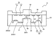
図1は本実施形態の光フィルター10の電圧非印加状態の断面図であり、図2は電圧印加状態の断面図である。図1及び図2に示す光フィルター10は、第1基板20と、第1基板10と対向する第2基板30とを含む。本実施形態では、第1基板20を固定基板とし、第2基板30を可動基板またはダイヤフラムとするが、いずれか一方又は双方が可動であれば良い。
1. Optical filter 1.1. Filter section of optical filter 1.1.1. FIG. 1 is a cross-sectional view of the
本実施形態では、第1基板20と例えば一体で、第2基板30を可動に支持する支持部23が形成されている。支持部20は、第2基板30に設けても良く、あるいは第1,第2基板20,30とは別体で形成しても良い。
In the present embodiment, a
第1,第2基板20,30は、それぞれ例えば、ソーダガラス、結晶性ガラス、石英ガラス、鉛ガラス、カリウムガラス、ホウケイ酸ガラス、無アルカリガラスなどの各種ガラスや、水晶などにより形成されている。これらの中でも、各基板20,30の構成材料としては、例えばナトリウム(Na)やカリウム(K)などのアルカリ金属を含有したガラスが好ましく、このようなガラスにより各基板20,30を形成することで、後述する反射膜40,50や、各電極60,70の密着性や、基板同士の接合強度を向上させることが可能となる。そして、これらの2つの基板20,30は、例えばプラズマ重合膜を用いた表面活性化接合などにより接合されることで、一体化されている。第1,第2基板20,30の各々は、一辺が例えば10mmの正方形に形成され、ダイヤフラムとして機能する部分の最大直径は例えば5mmである。
The first and
第1基板20は、厚みが例えば500μmに形成されるガラス基材をエッチングにより加工することで形成される。第1基板20は、第2基板30と対向する第1対向面20Aのうちの中央の第1面20A1に、例えば円形の第1反射膜40が形成されている。同様に、第2基板30は、厚みが例えば200μmに形成されるガラス基材をエッチングにより加工することで形成される。第2基板30は、第1基板20と対向する第2対向面30Aの中央位置に、第1反射膜40と対向する例えば円形の第2反射膜50が形成されている。
The
なお、第1,第2反射膜40,50は、例えば直径が約3mmの円形状に形成されている。この第1,第2反射膜40,50は、AgC単層により形成される反射膜であり、スパッタリングなどの手法により第1,第2基板20,30に形成することができる。AgC単層反射膜の膜厚寸法は、例えば0.03μmに形成されている。本実施形態では、第1,第2反射膜40,50として、可視光全域を分光できるAgC単層の反射膜を用いる例を示すが、これに限定されず、分光可能な波長域が狭いが、AgC単層反射膜よりも、分光された光の透過率が大きく、透過率の半値幅も狭く分解能が良好な、例えばTiO2とSiO2との積層膜を積層した誘電体多層膜を用いてもよい。
The first and
さらに、第1,第2基板20,30の第1,第2対向面20A,30Aとは逆側の面にて、第1,第2反射膜40,50に対応する位置に図示しない反射防止膜(AR)を形成することができる。この反射防止膜は、低屈折率膜および高屈折率膜を交互に積層することで形成され、第1,第2基板20,30の界面での可視光の反射率を低下させ、透過率を増大させる。
Further, on the surface opposite to the first and second opposing
これら第1,第2反射膜40,50は、図1に示す電圧非印加状態にて第1ギャップG1を介して対向配置されている。なお、本実施形態では、第1反射膜40を固定鏡とし、第2反射膜50を可動鏡とするが、上述した第1,第2基板20,30の態様に応じて、第1,第2反射膜のいずれか一方又は双方を可動とすることができる。
The first and second
平面視で第1反射膜40の周囲の位置であって、第1基板20の第1対向面20A1の周囲の第2対向面20A2には、第1電極60が形成されている。同様に、第2基板30の対向面30Aには、第1電極60と対向して第2電極70が設けられている。第1電極60と第2電極70は、第2ギャップG2を介して、対向配置されている。なお、第1,第2電極60,70の表面は、絶縁膜にて被覆することができる。
A
本実施形態では、第1基板20が第2基板30と対向する第1対向面20Aは、第1反射膜40が形成される第1面20A1と、平面視で第1面20A1の周囲に配置されて、第1電極60が形成される第2面20A2とを有する。第1面20A1と第2面20A2とは同一面でなく、第1面20A1と第2面20A2との間には段差22があり、第1面20A1の方が第2面20A2よりも第2基板30に近い位置に設定している。これにより、電圧の無印加状態での初期値にて、第1ギャップG1<第2ギャップG2の関係が成立する。
In the present embodiment, the first facing
ここで、上述した式(1)から、静電引力Fは第1,第2電極60,70間のギャップG(第2ギャップG2)の二乗に反比例する。静電引力Fの変化量ΔFと、第1,第2電極60,70間のギャップGの変化量ΔGとの関係を、図3に示す。図3では、電極間ギャップGが小さい領域でのギャップ変化量ΔG1と、電極間ギャップGが大きい領域でのギャップ変化量ΔG2(=ΔG1)とが示されている。電極間ギャップGが小さい領域では、ギャップがギャップ変化量ΔG1だけ変化するだけで、静電引力FはΔF1と大きく変化する。これに対して、電極間ギャップGが大きい領域では、ギャップ変化量ΔG1と同じギャップ変化量ΔG2だけ変化しても、静電引力Fの変化量は比較的小さいΔF2となる。
Here, from the above-described equation (1), the electrostatic attractive force F is inversely proportional to the square of the gap G (second gap G2) between the first and
このように、電極間ギャップGが比較的狭い領域では、ギャップGがわずかに変化しただけで静電引力Fが急激に変化し、所定の静電引力Fを得るためのギャップ制御が極めて困難である。これに対して、電極間ギャップGが比較的広い領域では、ギャップ変化単位量に対する静電引力Fの変化が小さい。よって、図3のF−G特性カーブのうち静電引力Fの変化が小さい平坦な領域(電極間ギャップGが比較的広い領域)を使用した方が、電圧間ギャップGによって静電引力Fの大きさを制御し易いことが分かる。 As described above, in the region where the gap G between the electrodes is relatively narrow, the electrostatic attractive force F changes abruptly only by changing the gap G slightly, and it is extremely difficult to control the gap to obtain the predetermined electrostatic attractive force F. is there. On the other hand, in the region where the interelectrode gap G is relatively wide, the change in the electrostatic attractive force F with respect to the gap change unit amount is small. Therefore, in the FG characteristic curve shown in FIG. 3, when the flat region where the change in the electrostatic attractive force F is small (the region where the interelectrode gap G is relatively wide) is used, It can be seen that the size is easy to control.
一方、可変波長対象の透過波長帯域は後述するように例えば380〜700nmであって、第1,第2反射膜40,50間の第1ギャッブG1は140〜300nmと小さい。そこで、図1のように、第1ギャップG1<第2ギャップG2に設定して、静電引力Fの大きさを制御し易くしている。
On the other hand, the transmission wavelength band for the variable wavelength target is, for example, 380 to 700 nm as described later, and the first gap G1 between the first and
第1電極60は、例えば電気的に独立した少なくともK(Kは2以上の整数)個のセグメント電極に分割され、本実施形態ではK=2の例として第1,第2のセグメント電極62,64を有することができる。つまり、K個のセグメント電極62,64はそれぞれ、異なる電圧に設定可能である一方で、第2電極30は、同電位となる共通電極である。なお、K≧3の場合には、第1,第2セグメント電極62,64に関して以下にて説明する関係は、相隣り合う任意の2つのセグメント電極について適用することができる。なお、本発明は第1電極60を必ずしもK個のセグメント電極に分割するものに限らない。第1電極60を非分割した実施例については、図15〜図18にて後述する。
The
このような構造の光フィルター10は、第1,第2基板20,30が共に、反射膜(第1,第2反射膜40,50)が形成される領域と、電極(第1,第2電極60,70)が形成される領域とは、平面視で異なる領域となり、特許文献1のように反射膜と電極とが積層されることはない。よって、第1,第2基板20,30の少なくとも一方(本実施形態では第2基板30)が可動基板とされても、反射膜と電極とが積層されないために可動基板は撓み易さを確保できる。しかも、特許文献1とは異なり、第1,第2電極60,70上には反射膜が形成されないので、透過型または反射型波長可変干渉フィルターとしての光フィルター10を利用しても、第1,第2電極60,70を、透明電極とする制約も生じない。なお、透明電極であっても透過特性には影響を与えるため、第1,第2電極60,70上に反射膜が形成されてない事によって、透過型または反射型波長可変干渉フィルターである光フィルター10は所望の透過または反射特性が得られる。
In the
また、この光フィルター10では、平面視で第2反射膜50の周囲に配置された第2電極70に共通電圧(例えば接地電圧)を印加し、平面視で第1反射膜40の周囲に配置された第1電極60を構成するK個のセグメント電極62,64の個々に独立した電圧を印加して、図2に示すように対向電極間に矢印で示す静電引力F1,F2を作用させることで、第1,第2反射膜40,50間の第1ギャップG1を初期ギャップの大きさよりも小さいギャップとなるように可変する。
Further, in this
つまり、電圧印加状態の光フィルター10を示す図2の通り、第1セグメント電極62及びそれと対向する第2電極70とで構成される第1ギャップ可変駆動部(静電アクチュエーター)80と、第2セグメント電極64及びそれと対向する第2電極70とで構成される第2ギャップ可変駆動部(静電アクチュエーター)90とが、それぞれ独立して駆動される。
That is, as shown in FIG. 2 showing the
このように、平面視で第1,第2反射膜40,50の周囲にのみ配置された独立する複数(K個)のギャップ可変駆動部80,90を有することで、K個のセグメント電極62,64に印加する電圧の大きさと、K個のセグメント電極62,64の中から電圧を印加するために選択されたセグメント電極数との、2つのパラメーターを変化させることで、第1,第2反射膜40,50間のギャップの大きさを制御する。
As described above, the
特許文献1のように、パラメーターが電圧の種類だけでは、大きなギャップ可動範囲と、ノイズ等による電圧変動に対する低感度とを、両立することが困難であった。本実施形態のように、電極数というパラメーターを加えることで、電圧だけで制御する場合と同じ印加電圧範囲を個々のセグメント電極に適用することで、大きなギャップ可動範囲の中で、より微調整された静電引力を発生させて、精細なギャップ調整を行うことが可能となる。
As in
ここで、印加電圧の最大値をVmaxとし、ギャップをN段階で可変するものとする。第1電極60が複数に分割されていない場合には、最大電圧VmaxをN分割して印加電圧を割り当てる必要がある。このとき、異なる印加電圧間の電圧変化量の最小値をΔV1minとする。一方、本実施形態では、K個のセグメント電極の各々への印加電圧は、最大電圧Vmaxを平均的には(N/K)分割して割り当てればよい。このとき、K個のセグメント電極の各々について、同一セグメント電極に印加される異なる印加電圧間の電圧変化量の最小値をΔVkminとする。その場合、ΔV1min<ΔVkminが成立することが明らかである。
Here, it is assumed that the maximum value of the applied voltage is Vmax and the gap is variable in N stages. When the
このように、電圧最小変化量ΔVkminを大きく確保できれば、電源変動や環境等に依存したノイズによってK個のセグメント電極62,64への印加電圧が多少変動してもギャップ変動は小さくなる。つまり、ノイズに対する感度が小さい、換言すれば電圧感度が小さくなる。それにより、高精度なギャップ制御が可能となり、特許文献1のようにギャップを帰還制御することは必ずしも要しない。また、ギャップを帰還制御したとしても、ノイズに対する感度が小さいために早期に安定させることができる。
本実施形態では、中央側の第1,第2反射膜40,50の領域は非駆動領域とし、その周囲を駆動領域とすることで、第1,第2反射膜40,50の平行度を維持している。第1,第2反射膜40,50の平行度は、第1,第2反射膜40,50間で多重反射させて干渉により不要波長の光を減衰させるファブリペロー型干渉フィルターにとっては重要な技術要素である。
In this way, if the minimum voltage change amount ΔVkmin can be secured large, the gap fluctuation becomes small even if the voltage applied to the
In the present embodiment, the first and second
本実施形態では、可動基板である第2基板30の撓み性を確保するために、図1に示すように、第2電極70が形成される領域を例えば厚み寸法が50μm程度の薄肉部34としている。この薄肉部34は、第2反射膜40が配置される領域の厚肉部32、および支持部23と接触する領域の厚肉部36よりも肉薄に形成されている。換言すれば、第2基板30は、第2反射膜40及び第2電極70が形成される第2対向面30Aは平坦面であり、第2反射膜40が配置される第1領域に厚肉部32が形成され、第2電極70が形成される第2領域に薄肉部34が形成される。こうして、薄肉部34にて撓み性を確保しながら、厚肉部32を撓み難くすることで、第2反射膜40は平面度を保ってギャップを可変することが可能となる。第2基板30に段部や局所的に厚肉部を設ける例については後述する。
In the present embodiment, in order to ensure the flexibility of the
なお、本実施形態では、独立した複数(K個)のギャップ可変駆動部はそれぞれ、一対の電極からなる静電アクチュエーターで構成したが、それらの少なくとも一つを圧電素子等の他のアクチュエーターに置き換えても良い。ただし、非接触で吸引力を与える静電アクチュエーターは、複数あるギャップ可変駆動部同士の干渉が少なく、ギャップを高精度に制御する上で適している。これとは異なり、例えば2つの圧電素子を第1,第2基板20,30間に配置した場合、駆動していない圧電素子が、他の駆動している圧電素子によるギャップ変位を妨げる存在となる等が生じ、複数のギャップ可変駆動部を独立して駆動する方式にとっては弊害を生じる。その点から、複数のギャップ可変駆動部は静電アクチュエーターで構成することが好ましい。
In the present embodiment, each of the plurality of independent (K) variable gap drive units is constituted by an electrostatic actuator composed of a pair of electrodes, but at least one of them is replaced with another actuator such as a piezoelectric element. May be. However, the electrostatic actuator that applies a suction force in a non-contact manner is suitable for controlling the gap with high accuracy because there is little interference between the plurality of gap variable drive units. On the other hand, for example, when two piezoelectric elements are arranged between the first and
1.1.2. 第1電極
第1電極60を構成するK個のセグメント電極62,64は、図4(A)の通り、第1反射膜40の中心に対して同心リング状に配置することができる。つまり、第1セグメント電極62は第1リング状電極部62Aを有し、第2セグメント電極64はリング状電極部62Aの外側に第2リング状電極部64Aを有し、各リング状電極部62A,64Aが第1反射膜に対して同心リング状に形成される。なお、「リング状」とは、無端リングに限らず不連続リング形状も含み、円形リングに限らず矩形リングまたは多角形リング等を含む用語である。
1.1.2. First Electrode The
こうすると、図2に示すように、第1反射膜40の中心線Lに対して、第1,第2セグメント電極の各々が線対称配置となる。これにより、電圧印加時に第1,第2電極60,70間に作用する静電引力F1,F2は、第1反射膜40の中心線Lに対して線対称に作用するので、第1,第2反射膜40,50の平行度が高まる。
As a result, as shown in FIG. 2, the first and second segment electrodes are arranged symmetrically with respect to the center line L of the first
なお、図4(A)に示すように、第2セグメント電極64のリング幅W2は、第1セグメント電極62のリング幅W1よりも広くすることができる(W2>W1)。静電引力は電極面積に比例し、第2セグメント電極64により生じさせる静電引力F2の方が、第1セグメント電極62により生じさせる静電引力F1よりも大きく求められるからである。さらに詳しく言えば、外側の第2セグメント電極64は、ヒンジ部として機能する基板支持部23に対して第1セグメント電極62よりも近くに設けられる。このため、第2セグメント電極64はヒンジ部40での抵抗力に抗する大きな静電引力F2を発生する必要がある。外側の第2セグメント電極64は、内側の第1セグメント電極62に比べて直径が大きく、幅W1=幅W2であっても第2セグメント電極64の面積は大きい。よって、幅W1=幅W2としてもよいが、リング幅W2をより広げることにより、更に面積を増大させて大きな静電引力F2の発生を可能とした。特に、後述するように、外側の第2セグメント電極64を内側の第1セグメント電極62よりも先に駆動する場合には、第2セグメント電極64と第2電極70との間の初期ギャップG2が大きいので、第2セグメント電極64の面積を広くして大きな静電引力F2を発生できる点でも有利となる。その場合、内側の第1セグメント電極62の駆動時には、第1セグメント電極64の駆動状態が維持されている限りギャップは小さくなっているので、第1セグメント電極62のリング幅W1は小さくても駆動上の弊害はない。
As shown in FIG. 4A, the ring width W2 of the
ここで、第1セグメント電極62には第1引き出し配線62Bが、第2セグメント電極64には第2引き出し電極64Bがそれぞれ接続される。これら第1,第2引き出し電極62B,64Bは例えば第1反射膜40の中心から放射方向に向けて延在形成される。第2セグメント電極64の第2リング状電極部64Aを不連続とする第1スリット64Cが設けられている。内側の第1セグメント電極62から延びる第1引き出し配線62Bは、外側の第2セグメント電極64に形成された第1スリット64Cを介して、第2セグメント電極64の外方に引き出される。
Here, the
このように、第1,第2セグメント電極62,64をそれぞれリング状電極部62A,64Aとした場合に、外側の第2セグメント電極64に形成された第1スリット64Cより、内側の第1セグメント電極62の第1引き出し配線62Bの取り出し経路を容易に確保できる。
Thus, when the first and
1.1.3. 第2電極
第2基板30に配置された第2の電極70は、第2基板30のうち、第1基板20に形成された第1電極60(第1,第2セグメント電極62,64)と対向する領域を含む域にベタ電極として形成することができる。第2電極70は同一電圧に設定される共通電極だからである。
1.1.3. Second Electrode The
これに代えて、本実施形態のように第1基板20に対して変位する第2基板30に配置された第2の電極70は、第1電極60と同様に、K個のセグメント電極とすることができる。このK個のセグメント電極もまた、第2反射膜50の中心に対して同心リング状に配置することができる。こうすると、可動である第2基板30に形成される電極面積は、必要最小限に縮小されるので、第2基板30の剛性が低くなり、撓み易さを確保できる。
Instead, the
第2電極70を構成するK個のセグメント電極は、図1、図2及び図4(B)に示すように、弟3セグメント電極72及び第4セグメント電極74を有することができる。第3セグメント電極72は第3リング状電極部72Aを有し、第4セグメント電極74は第3リング状電極部62Aの外側に第4リング状電極部74Aを有し、各リング状電極部72A,74Aが第2反射膜に対して同心リング状に形成される。「同心リング状」の意味は、第1電極60に対するものと同一である。第3セグメント電極72は第1セグメント電極62と対向し、第4セグメント電極74は第2セグメント電極64と対向している。よって、本実施形態では第4セグメント電極74のリング幅(第2セグメント電極64のリング幅W2と同じ)は、第3セグメント電極72のリング幅(第1セグメント電極62のリング幅W1と同じ)よりも広い。
The K segment electrodes constituting the
また、第3,第4セグメント電極72,74同士は電気的に接続されて、同一電位に設定される。このために、例えば第3,第4引き出し電極76A,76Bが例えば第2反射膜50の中心から放射方向に向けて延在形成される。第3,第4引き出し電極76A,76Bの各々は、内側の第3セグメント電極72と外側の第4セグメント電極74の双方と電気的に接続される。なお、共通電極である第3.第4セグメント電極72,74は1本の引き出し電極により接続されても良いが、引き出し電極を複数とすることで配線抵抗を少なくして、共通電極の充放電速度を速めることができる。
The third and
1.1.4. 第1,第2電極の重合領域
図5(A)は、本実施形態の第1,第2電極60,70を第2基板30側から見た平面視での重なり状態を示している。図5(A)において、下側に位置する第1電極60は、第1,第2セグメント電極62,64が第2電極の第3,第4セグメント電極72,74と対向しているため、第2基板30側から見た平面視では現れない。下側に位置する第1電極は、ハッチングで示すように第1,第2引き出し配線62B,64Bのみが、第2基板30側から見た平面視で現れている。第1引き出し配線62Bは、第2電極70の第3リング状電極部74Aが周方向で連続するので、中間領域62B1が第3リング状電極部74Aの対向領域74A1と対向する。
1.1.4. Overlapping Region of First and Second Electrodes FIG. 5A shows the overlapping state in plan view when the first and
本実施形態では、図4(A)に示すように、第1電極20のうちの外側の第2セグメント電極64は、第1スリット64Cを有するので、このスリット64Cの領域では第2セグメント電極64に印加した電圧に基づく静電引力F2(図2参照)は作用しない。
In the present embodiment, as shown in FIG. 4A, the
一方、この第1スリット64C内には図4(A)に示すように第1引き出し配線62Bが配置されるので、内側の第1セグメント電極62と同電位である第1引き出し配線62Bと、外側の第4セグメント電極74間に作用する静電引力F1(図2参照)を第1スリット64C内にて生じさせることができる。その利点として、例えば第1,第2セグメント電極62,64を実質的に同電圧で駆動した場合には、外側の第4セグメント電極74のほぼ全周(第1スリット64Cとの対向領域74A1を含む)に均等な静電引力を生じさせることができる。
On the other hand, as shown in FIG. 4A, the first lead-out
図5(B)は、変形例である第1,第2電極60,70’を第2基板30側から見た平面視での重なり状態を示している。図5(B)の第2電極70’が図5(A)の第2電極70と相違する点は、第4セグメント電極74が、第1電極60の第1スリット64Cと対向する位置にて第4リング状電極部74A’を不連続とする第2スリット78をさらに有する点である。その余の点では、図5(B)の第2電極70’は図5(A)の第2電極70と同一である。
FIG. 5B shows an overlapping state in a plan view of the first and
こうすると、第1引き出し配線62Bと対向する電極が存在しなくなる。よって、例えば、内側の第1セグメント電極62を駆動した時、内側の第1セグメント電極62と同電位である第1引き出し配線62Bと、外側の第4セグメント電極74’間に作用する不要な静電引力が、第1スリット64C内で発生することを阻止できる。
As a result, there is no electrode facing the first
1.1.5. 引き出し配線
図6は、第2基板30側から第2基板30を透視して平面図であり、第1〜第4引き出し配線62B,64B,76A,76Bの配線レイアウトを示している。図6において、第1,第2基板20,30の少なくとも一方が、第1及び第2対角線を有する矩形基板とされる。本実施形態では、第1,第2基板20,30の各々が、一辺が例えば10mmの正方形に形成されている。第1引き出し配線62Bが、第1対角線に沿って第1セグメント電極62Aより延びる方向を第1方向D1としたとき、第2引き出し配線64Bは、第1対角線上にて第1方向D1とは逆方向となる第2方向D2に延びている。第3引き出し配線76Aは、第2対角線に沿った第3方向D3に延びている。第4引き出し配線76Bは、第2対角線上にて第3方向D3とは逆方向となる第4方向D4に延びている。そして、平面視にて矩形基板20,30の四隅の位置にて、第1〜第4引き出し配線62B,64B,76A,76Bが接続される第1〜第4接続電極部101〜104が設けられている。
1.1.5. Drawing Wiring FIG. 6 is a plan view of the
こうすると、先ず、第1基板20に形成される第1,第2引き出し配線62B,64Bと、第2基板30に形成される第3,第4引き出し配線76A,76Bとは、平面視で重なり合うことはなく、平行電極を構成しない。よって、第1,第2引き出し配線62B,64Bと、第3,第4引き出し配線76A,76Bとの間に無駄な静電引力が生じず、また、無駄な容量を持たない。更に、第1〜第4接続電極部101〜104にそれぞれ至る第1〜第4引き出し配線62B,64B,76A,76Bの配線長が最短となる。よって、第1〜第4引き出し配線62B,64B,76A,76Bの配線抵抗及び配線容量が小さくなり、第1〜第4セグメント電極62,64,72,74を高速に充放電することができる。
In this way, first, the first and second
なお、第1〜第4外部接続電極部101〜104は、第1,第2基板20,30のいずれか一方か、あるいは双方に各一部を設けても良い。第1,第2基板20,30のいずれか一方にのみ第1〜第4外部接続電極部101〜104を設ける場合には、第1,第2基板20,30の他方に配置された引き出し配線は、導電性ペースト等によって一方の基板に形成された外部接続電極部に接続することができる。なお、第1〜第4外部接続電極部101〜104は、リード線またはワイヤボンディング等の接続部を介して、外部と接続される。
The first to fourth external
また、第1〜第4引き出し配線62B,64B,76A,76Bは、第1,第2基板20,30を接合する例えばプラズマ重合膜と交差してもよい。あるいは、第1,第2基板20,30の接合面の一方に設けた溝部を介して、第1〜第4引き出し配線62B,64B,76A,76Bを、接合面を超えて外部に引き出しても良い。
Further, the first to fourth
1.2. 光フィルターの電圧制御系
1.2.1. 印加電圧制御系ブロックの概要
図7は、光フィルター10の印加電圧制御系ブロック図である。図7に示すように、光フィルター10は、第1電極60と第2電極70との間の電位差を制御する電位差制御部110を有する。本実施形態では、共通電極である第2電極70(第3,第4セグメント電極72,74)は一定の共通電圧例えば接地電圧(0V)に固定されているため、電位差制御部110は、第1電極60を構成するK個のセグメント電極である第1,第2セグメント電極62,64への印加電圧を変化させて、第1,第2セグメント電極62,64の各々と第2電極70との間の内周側電位差ΔVseg1及び外周側電位差ΔVseg2をそれぞれ制御する。なお、第2電極70は接地電圧以外の共通電圧を印加してもよく、その場合、電位差制御部110が第2電極70に共通電圧の印加/非印加を制御しても良い。
1.2. Voltage control system of optical filter 1.2.1. Overview of Applied Voltage Control System Block FIG. 7 is an applied voltage control system block diagram of the
図7では、電位差制御部110は、第1セグメント電極62に接続された第1セグメント電極駆動部例えば第1デジタル−アナログコンバータ(DAC1)112と、第2セグメント電極64に接続された第2セグメント電極駆動部例えば第2デジタル−アナログコンバータ(DAC2)114と、それらを制御例えばデジタル制御するデジタル制御部116とを含んでいる。第1,第2デジタル−アナログコンバータ112,114には電源120からの電圧が供給される。第1,第2デジタル−アナログコンバータ112,114は、電源120からの電圧の供給を受けると共に、デジタル制御部116からのデジタル値に応じたアナログ電圧を出力する。電源120は、光フィルター10が装着される分析機器または光機器に装備されているものを利用できるが、光フィルター10専用の電源を用いても良い。
In FIG. 7, the potential
1.2.2. 光フィルターの駆動方法
図8は、図7に示すデジタル制御部116での制御の元データである電圧テーブルデータの一例を示す特性図である。この電圧テーブルデータは、デジタル制御部116自体に設けても良いし、あるいは光フィルター10が装着される分析機器または光機器に装備しても良い。
1.2.2. Optical Filter Driving Method FIG. 8 is a characteristic diagram showing an example of voltage table data which is original data for control in the
図8は、K個のセグメント電極62,64の各々に順次電圧を印加することで、計N段階で第1,第2反射膜40,50の間のギャップを可変するための電圧テーブルデータとして、N=9の例を示している。なお、図8では、第1,第2セグメント電極62,64の双方と第2電極70との間の各電位差が共に0Vであるときは、N段階のギャップ可変範囲に含めていない。図8は、第1,第2セグメント電極62,64の少なくとも一方に、第2電極70に印加される共通電圧の電圧値(0V)以外の電圧値が印加される場合のみを示している。ただし、第1,第2セグメント電極62,64の双方と第2電極70との間の各電位差が共に0Vであるときを、透過ピーク波長が最大であると定義しても良い。
FIG. 8 shows voltage table data for changing the gap between the first and second
電位差制御部110は、図8に示す電圧テーブルデータに従って、K個のセグメント電極(第1,第2セグメント電極62,64)毎に設定された電圧値を、K個のセグメント電極(第1,第2セグメント電極62,64)の各々に印加している。図9は、図8に示す電圧テーブルデータのデータ番号順に駆動することで実現される電圧印加のタイミングチャートである。
In accordance with the voltage table data shown in FIG. 8, the potential
図8及び図9に示すように、第1セグメント電極62には、L=4種類の電圧(VI1〜VI4:VI1<VI2<VI3<VI4)を印加し、第2セグメント電極64には、M=5種類の電圧(VO1〜VO5:VO1<VO2<VO3<VO4<VO5)を印加し、第1,第2反射膜40,50の間の第1ギャップG1をg0〜g8の9(N=L+M=9)段階にて可変している。
As shown in FIGS. 8 and 9, L = 4 kinds of voltages (VI1 to VI4: VI1 <VI2 <VI3 <VI4) are applied to the
このような電圧制御により、光フィルター10では、図10に示す波長透過特性を実現できる。図10は、第1,第2反射膜40,50間の第1ギャップG1の大きさを例えばg0〜g3に変化した時の波長透過特性を示している。光フィルター10では、第1,第2反射膜40,50の間の第1ギャップG1の大きさが例えばg0〜g3(g0>g1>g2>g3)と可変されると、その第1ギャップG1の大きさに応じて透過ピーク波長が決定される。すなわち、光フィルター10を透過する光の波長λは、その半波長(λ/2)の整数(n)倍が第1ギャップG1と一致する光であり(n×λ=2G1)、半波長(λ/2)の整数(n)倍が第1ギャップG1と一致しない光は、第1,第2反射膜40,50により多重反射される過程で干渉しあって減衰され、透過することがない。
By such voltage control, the
したがって、図10に示すように、第1,第2反射膜40,50間の第1ギャップG1の大きさをg0、g1、g2、g3と狭めるように変化させることで、光フィルター10を透過する光、すなわち透過ピーク波長がλ0、λ1、λ2、λ3(λ0>λ1>λ2>λ3)と、順次短くなるように変化する。
Therefore, as shown in FIG. 10, the size of the first gap G1 between the first and second
ここで、L,M,Nの値は任意に変更できるが、L≧3,M≧3、N≧6の整数とすることが好ましい。L≧3,M≧3、N≧6とすると、第1,第2セグメント電極62,64毎に設定されている、第1電位差ΔV1から、第1電位差ΔV1より大きい第2電位差ΔV2、第2電位差ΔV2より大きい第3電位差ΔV3へと、内周側電位差ΔVseg1及び外周側電位差ΔVseg2をそれぞれ切り替えることができる。
Here, the values of L, M, and N can be arbitrarily changed, but are preferably integers of L ≧ 3, M ≧ 3, and N ≧ 6. When L ≧ 3, M ≧ 3, and N ≧ 6, the second potential difference ΔV2 that is set for each of the first and
図8に示すように、電位差制御部110は、先ず、外側の第2セグメント電極64に電圧VO1〜電圧VO5を順次印加する。第2電極70が0Vであることから、第2電極70と第2セグメント電極64との間の電位差は、第1電位差VO1、第2電位差VO2、第3電位差VO3、第4電位差VO4、第5電位差VO5と、外周側電位差Vseg2を順次大きくすることができる。それにより、第1,第2反射膜40,50間の第1ギャップG1の大きさが、go→g1→g2→g3→g4と順次小さくなる。この結果、光フィルター10を透過する光、すなわち透過ピーク波長がλ0→λ1→λ2→λ3→λ4と、順次短くなるように変化する。
As shown in FIG. 8, the potential
次に電位差制御部110は、図8に示すように、第2セグメント電極64への最大印加電圧VO5の印加を維持したまま、電位差制御部110は、内側の第1セグメント電極62電圧VI1〜電圧VI4を順次印加する。第2電極70が0Vであることから、第2電極70と第1セグメント電極62との間の電位差は、第1電位差VI1、第2電位差VI2、第3電位差VI3、第4電位差VIO4と、内周側電位差Vseg1を順次大きくすることができる。それにより、第1,第2反射膜40,50間の第1ギャップG1の大きさが、g5→g6→g7→g8と順次小さくなる。この結果、光フィルター10を透過する光、すなわち透過ピーク波長がλ5→λ6→λ7→λ8と、順次短くなるように変化する。
Next, as shown in FIG. 8, the potential
電位差制御部110は、外周側電位差Vseg2ついて少なくとも、第1電位差VO1から、第1電位差VO1より大きい第2電位差VO2へ、さらに第2電位差VO2よりも大きい第3電位差VO3に切り替え、内周側電位差Vseg1について少なくとも、第1電位差VI1から、第1電位差VI1より大きい第2電位差VI2へ、さらに第2電位差VI2よりも大きい第3電位差VI3に切り替えるため、可動側の第2基板30の減衰自由振動を抑制することができ、迅速な波長可変動作が実施することができる。しかも、電位差制御部110は、第1,第2セグメント電極62,64の各々に対して3値以上の電圧0を含んでも良い)として、第1セグメント電極62に対して少なくとも第1セグメント電圧VI1、第2セグメント電圧VI2及び第3セグメント電圧VI3を、第2セグメント電極64に対して少なくとも第1セグメント電圧VO1、第2セグメント電圧VO2及び第3セグメント電圧VO3を印加している。よって、第1,第2セグメント電極62,64の各一つを駆動するだけで、それぞれ3段階以上のギャップ可変が可能となり、第1電極60のセグメント電極数を無用に多くする必要がない。
The potential
1.2.3. 電圧変化量(第1電位差と第2電位差との差の絶対値等)
電位差制御部110は、内周側電位差Vseg1及び外周側電位差Vseg2の各々について、第2電位差と第3電位差との差の絶対値を、第1電位差と第2電位差との差の絶対値よりも小さくすることができる。本実施形態では第2電極70は共通電圧0Vで不変であるので、例えば外周側電位差Vseg2としての第1電位差と第2電位差との差の絶対値とは、図8及び図9に示すように、第2セグメント電極64に印加される第1セグメント電圧VO1及び第2セグメント電圧VO2間の電圧変化量ΔVO1と等価である。図8及び図9に示すように、外周側電位差Vseg2の電圧変化量は、ΔVO1>ΔVO2>ΔVO3>ΔVO4と順次小さくなる関係にあり、内周側電位差Vseg1の電圧変化量も、ΔVI1>ΔVI2>ΔVI3と順次小さくなる関係にある。
1.2.3. Voltage change amount (absolute value of difference between first potential difference and second potential difference, etc.)
The potential
このような関係にした理由は次の通りである。上述した式(1)から、静電引力Fは、第1,第2電極60,70間の電位差(本実施形態では第1電極60への印加電圧V)の二乗に比例する。図11は、電位差Vの二乗に比例する静電引力Fの特性図(F=V2の図)である。図11に示すように、電位差Vが大きくなる方向に、第1電位差、第2電位差、第3電位差と切り替えたとき、第1電位差と第2電位差との差の絶対値ΔV1と、第2電位差と第3電位差との絶対値の差ΔV2が同じ場合(図11ではΔV1=ΔV2)、静電引力の増加量ΔFは、ΔF1からΔF2へと急激に増大することになり、オーバーシュートの原因となる。
The reason for this relationship is as follows. From the above-described formula (1), the electrostatic attractive force F is proportional to the square of the potential difference between the first and
そこで、第2電位差と第3電位差との差の絶対値ΔV2は、第1電位差と第2電位差との差の絶対値ΔV2よりも小さくする。これにより、ギャップが狭くなった際の静電引力の急激な増大を抑制することができ、オーバーシュートをより抑制することができ、より迅速な波長可変動作を実現することができる。 Therefore, the absolute value ΔV2 of the difference between the second potential difference and the third potential difference is made smaller than the absolute value ΔV2 of the difference between the first potential difference and the second potential difference. As a result, a sudden increase in electrostatic attraction when the gap is narrowed can be suppressed, overshoot can be further suppressed, and more rapid wavelength variable operation can be realized.
1.2.4. 電圧印加期間
電位差制御部110は、内周側電位差Vseg1及び外周側電位差Vseg2の各々について、第2電位差に設定されている期間は、第1電位差に設定されている期間より長く、第3電位差に設定されている期間は、第2電位差に設定されている期間より長くすることができる。本実施形態では、図9に示すように、外周側電位差Vseg2について、第2電位差VO1の期間TO2は、第1電位差VO1の期間TO1よりも長く、第3電位差VO3の期間TO3は、第2電位差VO2の期間TO2よりも長く、TO1<TO2<TO3<TO4<TO5と順次長くなる関係にある。同様に、図9に示すように、内周側電位差Vseg1について、第2電位差VI1の期間TI2は、第1電位差VI1の期間TI1よりも長く、第3電位差VI3の期間TI3は、第2電位差VI2の期間TI2よりも長く、TI1<TI2<TI3<TI4と順次長くなる関係にある。
1.2.4. Voltage application period The potential
第1電位差よりも大きい第2電位差としたとき、または第2電位差より大きい第3電位差としたとき、第2基板30の復元力も大きくなる。このため、第2基板30が静止するまでの時間が長くなる。すなわち、第1,第2反射膜40,50間の第1ギャップG1が、定位置に安定するまでの時間が長くなる。これに対して、本実施形態のように、第2電位差に設定されている期間を、第1電位差に設定されている期間より長く、第3電位差に設定されている期間を、第2電位差に設定されている期間より長く設定することにより、第1ギャップG1を所定値に安定させることができる。
When the second potential difference is larger than the first potential difference, or when the third potential difference is larger than the second potential difference, the restoring force of the
1.2.5. 電位差、ギャップ及び可変波長の実施例1
図12は、図8に示す電位差、ギャップ及び可変波長の実施例1のデータを示す特性図である。図12のデータ番号1〜9は図8のデータ番号1〜9と同一である。図13は、図12に示す印加電圧とギャップとの関係を示す特性図である。図14は、図12に示す印加電圧と透過ピーク波長との関係を示す特性図である。
1.2.5. Example 1 of potential difference, gap and variable wavelength
FIG. 12 is a characteristic diagram showing data of Example 1 of the potential difference, gap, and variable wavelength shown in FIG.
図12では、透過ピーク波長の最大波長λ0=700nmから最小波長λ8=380nmの9段階で透過ピーク波長を可変するために、第1,第2反射膜40,50間の第1ギャップG1は最大ギャップg0=300nmから最小ギャップg8=140nmの9段階に可変されている(図13も参照)。これに対応して、透過ピーク波長は最大波長λ0から最小波長λ8までの9段階に可変されている(図14も参照)。しかも、図12では、最大ギャップg0から最小ギャップg8までの9段階のギャッブg0〜g8を等間隔(=40nm)に設定することにより、最大波長λ0から最小波長λ8までの9段階の波長λ0〜λ8も等間隔(=40nm)となっている。このように、第1,第2反射膜間の第1ギャップG1の大きさを一定量ずつ順次狭まるように変化させることで、透過ピーク波長も一定値ずつ短くなる。
In FIG. 12, the first gap G1 between the first and second
電位差制御部110が、外周側電位差Vseg2をVO1=16.9V、VO2=21.4V、VO3=25V、VO4=27.6V、VO5=29.8Vに順次設定し、VO5=29.8Vに維持したまま、内周側電位差Vseg1をVI1=16.4V、VI2=22.2V、VI3=26.3V、VI4=29.3Vに順次設定する。
The potential
なお、第1,第2反射膜40,50間の第1ギャップG1の大きさは、外周側電位差Vseg2に基づく静電引力F2よりも内周側電位差Vreg1に基づく静電引力F1の影響の方が大きい。よって、先ず内周側電位差Vseg1を変化させた後に、内周側電位差Vseg1を一定値に維持したまま外周側電位差Vseg2を変化させても、内周側電位差Vseg1による静電引力F1が支配的となって第1,第2反射膜40,50間のギャップは外周側電位差Vseg2の通りに変化しない。そこで、本実施形態では先ず外周側電位差Vseg2を変化させた後に、外周側電位差Vseg2を一定値に維持したまま内周側電位差Vseg1を変化させている。
The size of the first gap G1 between the first and second
電位差制御部110は、外周側電位差Vseg2が外周側最大電位差VO5に到達した後に、外周側電位差Vseg2を外周側最大電位差VO5に維持して内周側電位差Vseg1を変化させている。こうすると、外周側最大電位差VO5にて設定された第1ギャップG1からさらに、内周側電位差Vseg1の印加による1ステップ分のギャップ変化が可能となる。しかも、内周側電位差Vseg1を印加させた後には、既に外周側最大外周側電位差VO5に達しているので、外周側電位差Vseg2をさらに変化させる必要はない。よって、外周側電位差Vseg2を変化させる時には、内周側電位差Vseg1による支配的な静電引力F2の悪影響は生じない。
The potential
電位差制御部110が内周側電位差Vseg1を内周側最大電位差VI4に設定したとき、第1,第2反射膜40,50間の第1ギャップG1は最小間隔g8に設定される。外周側最大電位差VO5及び内周側最大電位差VI4の各々は、電位差制御部110に供給される最大電圧Vmaxを超えない範囲で実質的に等しくすることができる。本実施形態では、図7に示す電源120から例えば最大電圧Vmax=30Vが電位差制御部110に供給される。このとき、外周側最大電位差VO5は、最大電圧Vmax(30V)を越えない29.8Vに設定され、内周側最大電位差VI4もまた、最大電圧Vmax(30V)を越えない29.3Vに設定されている。
When the potential
図12では、内周側最大電位差VO5及び内周側最大電位差VI4との間には0.5Vの微小な相違があるが、実質的に同一と言える。この微小な相違は、内周側電位差Vseg1及び外周側電位差Vseg2の各々について最大電圧Vmax(30V)を越えない範囲のフルスケール(図13及び図14参照)で、等間隔の透過ピーク波長を得るように設計された結果である。内周側最大電位差VO5及び内周側最大電位差VI4を厳密に一致させるには、第1,第2セグメント電極62,64の面積比などを調整することで可能ではあるが、厳密に一致させる必要性は乏しい。なお、本実施形態の駆動法では、内周側最大電位差VO5及び内周側最大電位差VI4を実質的に等しくすることで、図5(A)にて説明したように、外側の第4セグメント電極74のほぼ全周(第1スリット64Cとの対向領域74A1を含む)に均等な静電引力を生じさせることができるという利点がある。
In FIG. 12, although there is a minute difference of 0.5 V between the inner peripheral maximum potential difference VO5 and the inner peripheral maximum potential difference VI4, it can be said that they are substantially the same. This minute difference is that the transmission peak wavelengths at equal intervals are obtained at full scale (see FIGS. 13 and 14) in a range not exceeding the maximum voltage Vmax (30 V) for each of the inner peripheral potential difference Vseg1 and the outer peripheral potential difference Vseg2. This is the result of the design. In order to make the inner circumference side maximum potential difference VO5 and the inner circumference side maximum potential difference VI4 exactly match, it is possible to adjust the area ratio of the first and
本実施形態では、電位差制御部110は、K=2個の第1,第2セグメント電極62,64の各々に順次電圧を印加することで、計N=9段階で第1,第2反射膜40,50間の第1ギャップG1を可変している。このとき、K=2個の第1,第2セグメント電極62,64のうち同一セグメント電極62(または64)に印加される各印加電圧間の電圧変化量の最小値をΔVkminと定義する。図8及び図12の例では、第1セグメント電極62についてはΔVkmin=ΔVI3=3.0Vであり、第2セグメント電極64についてはΔVkmin=ΔVO4=2.2Vである。電源ノイズが0.1V程度であることを考慮すると、この最小電圧値ΔVkminがノイズに対する感度が小さいことは、以下の比較例との比較からも明らかである。
In the present embodiment, the potential
1.2.6 電位差、ギャップ及び可変波長の実施例2
実施例2では、図15(A)(B)に示すように、実施例1の第1電極60に代えて図15(A)に示す第1電極61を、実施例1の第2電極70に代えて図15(B)に示す第2電極71を用いる。つまり、実施例2の第1,第2電極61,71はセグメント分割されていない。
1.2.6 Example 2 of potential difference, gap and variable wavelength
In Example 2, as shown in FIGS. 15A and 15B, the
図16は、図15(A)(B)に示す第1,第2電極61,71間の電位差と、それにより得られるギャップ及び可変波長のデータを示す特性図である。図16のデータ番号1〜9は図8及び図12のデータ番号1〜9と同一である。図17は、図16に示す印加電圧とギャップとの関係を示す特性図である。図18は、図16に示す印加電圧と透過ピーク波長との関係を示す特性図である。
FIG. 16 is a characteristic diagram showing the potential difference between the first and
図16でも、透過ピーク波長の最大波長λ0=700nmから最小波長λ8=380nmの9段階で透過ピーク波長を可変するために、第1,第2反射膜40,50間の第1ギャップG1は最大ギャップg0=300nmから最小ギャップg8=140nmの9段階に可変されている(図16も参照)。これに対応して、透過ピーク波長は最大波長λ0から最小波長λ8までの9段階に可変されている(図17も参照)。
Also in FIG. 16, the first gap G1 between the first and
ただし、実施例2では、単一電極である第1電極61に印加される9段階の電圧を、最大電圧Vmax(30v)のフルスケールの中で設定しなければならない。
However, in the second embodiment, the nine levels of voltage applied to the
実施例2のように、第1電極61を単一電極で形成した時のN=9段階の各印加電圧間の電圧最小変化量をΔV1minと定義する。図16の例では、ΔV1min=0.9Vである。電源ノイズが0.1V程度であることを考慮すると、実施例2の電圧最小変化量ΔV1minはノイズに対する感度が大きい。
As in the second embodiment, when the
実施例1の電圧最小変化量ΔVkminと実施例2の電圧最小変化量V1minとを比較すると、ΔV1min<ΔVkminが成立し、実施例1ではノイズに対する感度をより小さくできる。 Comparing the minimum voltage change amount ΔVkmin of the first embodiment with the minimum voltage change amount V1min of the second embodiment, ΔV1min <ΔVkmin is established, and in the first embodiment, sensitivity to noise can be further reduced.
2.光フィルターの変形例
図19は、図1の光フィルター10とは異なる光フィルター11を示している。図19に示す第1基板21は、図1にて第1電極60が形成される第2面20A2が、平面視にて第1反射膜40が形成される第1面20A1の周囲の第2−1面20A21と、平面視にて第2−1面20A21の周囲に配置されて第2−1面20A21とは段差24のある第2−2面20A22とを含む。
2. FIG. 19 shows an optical filter 11 different from the
第1セグメント電極62は第2−1面20A21に配置され、第2セグメント電極64は第2−2面20A22に配置され、第2セグメント電極64と第2電極70との間の初期のギャップG22が、第1セグメント電極62と前記第2電極70との間の初期のギャップG21と異なっている。
The
このような関係にした理由は、以下の通りである。初期のギャップG21,G22のうち、最初に駆動される例えば第2セグメント電極64と対応する初期のギャップG22は、その第2セグメント電極64と第2電極との間に作用する静電引力により狭められる。このとき、同時にギャップG21も狭められ、初期ギャップよりも小さくなる。よって、第1セグメント電極62を駆動する時には、ギャップG21は初期値よりも小さくなっている。
The reason for this relationship is as follows. Of the initial gaps G21 and G22, the initial gap G22 corresponding to, for example, the
ここで、仮に第2−1面20A21と第2−2面20A22とが面一であってギャップG21,G22の初期値が同一であるとする。この場合、例えば第2セグメント電極64を最初に駆動するときのギャップG22は、後に第1セグメント電極62を駆動するときのギャップG21よりも大きくなってしまう。よって、第2セグメント電極64を最初に駆動するときの静電引力を、第1セグメント電極64が駆動されたときの静電引力よりも過度に大きく設定しなければならなくなる。
Here, it is assumed that the 2-1 surface 20A21 and the 2-2 surface 20A22 are flush with each other and the initial values of the gaps G21 and G22 are the same. In this case, for example, the gap G22 when the
よって、この場合には図19に示すように、ギャップG22の初期値をギャップG21の初期値よりも小さくしておくと良い。なお、第1セグメント電極62を最初に駆動する場合には、ギャップG21の初期値をギャップG22の初期値よりも小さくしておけばよい。
Therefore, in this case, as shown in FIG. 19, the initial value of the gap G22 is preferably made smaller than the initial value of the gap G21. When the
3.分析機器
図20は、本発明に係る一実施形態の分析機器の一例である測色器の概略構成を示すブロック図である。
3. FIG. 20 is a block diagram illustrating a schematic configuration of a colorimeter that is an example of an analytical instrument according to an embodiment of the present invention.
図20において、測色器200は、光源装置202と、分光測定装置203と、測色制御装置204と、を備えている。この測色器200は、光源装置202から検査対象Aに向かって例えば白色光を射出し、検査対象Aで反射された光である検査対象光を分光測定装置203に入射させる。そして、分光測定装置203にて検査対象光を分光し、分光した各波長の光の光量を測定する分光特性測定を実施する。言い換えると、検査対象Aで反射された光である検査対象光を光フィルター(エタロン)10に入射させ、エタロン10から透過した透過光の光量を測定する分光特性測定を実施する。そして、測色制御装置204は、得られた分光特性に基づいて、検査対象Aの測色処理、すなわち、どの波長の色がどの程度含まれているかを分析する。
20, the
光源装置202は、光源210、複数のレンズ212(図1には1つのみ記載)を備え、検査対象Aに対して白色光を射出する。また、複数のレンズ212には、コリメーターレンズが含まれており、光源装置202は、光源210から射出された白色光をコリメーターレンズにより平行光とし、図示しない投射レンズから検査対象Aに向かって射出する。
The
分光測定装置203は、図20に示すように、エタロン10と、受光部としての受光部220と、駆動回路230と、制御回路部240と、を備えている。また、分光測定装置203は、エタロン10に対向する位置に、検査対象Aで反射された反射光(測定対象光)を、内部に導光する図示しない入射光学レンズを備えている。
As shown in FIG. 20, the
受光部220は、複数の光電交換素子により構成されており、受光量に応じた電気信号を生成する。そして、受光部220は、制御回路部240に接続されており、生成した電気信号を受光信号として制御回路部240に出力する。
The
駆動回路230は、エタロン10の第1電極60、第2電極70、および制御回路部240に接続される。この駆動回路230は、制御回路部240から入力される駆動制御信号に基づいて、第1電極60および第2電極70間に駆動電圧を印加し、第2基板30を所定の変位位置まで移動させる。駆動電圧としては、第1電極60と第2電極70との間に所望の電位差が生じるように印加されればよく、例えば、第1電極60に所定の電圧を印加し、第2電極70をアース電位としてもよい。駆動電圧としては、直流電圧を用いるのが好ましい。
The
制御回路部240は、分光測定装置203の全体動作を制御する。この制御回路部240は、図20に示すように、例えばCPU250、記憶部260などにより構成されている。そして、CPU250は、記憶部260に記憶された各種プログラム、各種データに基づいて、分光測定処理を実施する。記憶部260は、例えばメモリーやハードディスクなどの記録媒体を備えて構成され、各種プログラム、各種データなどを適宜読み出し可能に記憶する。
The
ここで、記憶部260には、プログラムとして、電圧調整部261、ギャップ測定部262、光量認識部263、および測定部264が記憶されている。なお、ギャップ測定部262は上述の通り省略しても良い。
Here, the
また、記憶部260には、第1ギャップG1の間隔を調整するために静電アクチュエーター80,90に印加する電圧値、およびその電圧値を印加する時間を関連付けた図8に示す電圧テーブルデータ265が記憶されている。
In addition, the
測色制御装置204は、分光測定装置203および光源装置202に接続されており、光源装置202の制御、分光測定装置203により取得される分光特性に基づく測色処理を実施する。この測色制御装置204としては、例えば汎用パーソナルコンピューターや、携帯情報端末、その他、測色専用コンピューターなどを用いることができる。
The color
そして、測色制御装置204は、図20に示すように、光源制御部272、分光特性取得部270、および測色処理部271などを備えて構成されている。
As shown in FIG. 20, the
光源制御部272は、光源装置202に接続されている。そして、光源制御部272は、例えば利用者の設定入力に基づいて、光源装置202に所定の制御信号を出力し、光源装置202から所定の明るさの白色光を射出させる。
The light
分光特性取得部270は、分光測定装置203に接続され、分光測定装置203から入力される分光特性を取得する。
The spectral
測色処理部271は、分光特性に基づいて、検査対象Aの色度を測定する測色処理を実施する。例えば、測色処理部271は、分光測定装置203から得られた分光特性をグラフ化し、図示しないプリンターやディスプレイなどの出力装置に出力するなどの処理を実施する。
The color
図21は、分光測定装置203の分光測定動作を示すフローチャートである。まず、制御回路部240のCPU250は、電圧調整部261、光量認識部263、および測定部264を起動させる。また、CPU250は、初期状態として、測定回変数nを初期化(n=0に設定)する(ステップS1)。なお、測定回変数nは、0以上の整数の値をとる。
FIG. 21 is a flowchart showing the spectroscopic measurement operation of the
この後、測定部264は、初期状態、すなわち、静電アクチュエーター80,90に電圧が印加されていない状態で、エタロン10を透過した光の光量を測定する(ステップS2)。なお、この初期状態における第1ギャップG1の大きさは、例えば分光測定装置の製造時において予め測定し、記憶部260に記憶しておいてもよい。そして、ここで得られた初期状態の透過光の光量、および第1ギャップG1の大きさを測色制御装置204に出力する。
Thereafter, the
次に、電圧調整部261は、記憶部260に記憶されている電圧テーブルデータ265を読み込む(ステップS3)。また、電圧調整部261は、測定回変数nに「1」を加算する(ステップS4)。
Next, the
この後、電圧調整部261は、電圧テーブルデータ265から、測定回変数nに対応する第1,第2セグメント電極62,64の電圧データ及び電圧印加期間データを取得する(ステップS5)。そして、電圧調整部261は、駆動回路230に駆動制御信号を出力し、電圧テーブルデータ265のデータに従って静電アクチュエーター80,90を駆動する処理を実施する(ステップS6)。
Thereafter, the
また、測定部264は、印加時間経過タイミングで、分光測定処理を実施する(ステップS7)。すなわち、測定部264は、光量認識部263により透過光の光量を測定させる。また、測定部264は、測定された透過光の光量と、透過光の波長とを関連付けた分光測定結果を測色制御装置204に出力する制御をする。なお、光量の測定は、複数回または全ての回数の光量のデータを記憶部260に記憶させておき、複数回毎の光量のデータまたは全ての光量のデータの取得後に、まとめて、それぞれの光量を測定してもよい。
In addition, the
この後、CPU250は、測定回変数nが最大値Nに達したか否かを判断し(ステップS8)、測定回変数nがNであると判断すると、一連の分光測定動作を終了する。一方,ステップS8において、測定回変数nがN未満である場合、ステップS4に戻り、測定回変数nに「1」を加算する処理を実施し、ステップS5〜ステップS8の処理を繰り返す。
Thereafter, the
4.光機器
図22は、本発明に係る一実施形態の光機器の一例である波長多重通信システムの送信機の概略構成を示すブロック図である。波長多重(WDM: Wavelength Division Multiplexing)通信では、波長の異なる信号は干渉し合わないという特性を利用して、波長が異なる複数の光信号を一本の光ファイバー内で多重的に使用すれば、光ファイバー回線を増設せずにデータの伝送量を向上させることができるようになる。
4). Optical Device FIG. 22 is a block diagram showing a schematic configuration of a transmitter of a wavelength multiplexing communication system which is an example of an optical device according to an embodiment of the present invention. In wavelength division multiplexing (WDM) communication, if multiple optical signals with different wavelengths are used in a single optical fiber by using the characteristic that signals with different wavelengths do not interfere with each other, The amount of data transmission can be improved without increasing the number of lines.
図22において、波長多重送信機300は、光源301からの光が入射される光フィルター10を有し、光フィルター10からは複数の波長λ0,λ1,λ2,…の光が透過される。波長毎に送信器311,312,313が設けられる。送信器311,312,313からの複数チャンネル分の光パルス信号は、波長多重装置321にて1つに合わせられて一本の光ファイバー伝送路331に送出される。
In FIG. 22, the wavelength
本発明は光符号分割多重(OCDM: Optical Code Division Multiplexing)送信機にも同様に適用できる。OCDMは、符号化された光パルス信号のパターンマッチングによってチャンネルを識別するが、光パルス信号を構成する光パルスは、異なる波長の光成分を含んでいるからである。 The present invention can be similarly applied to an optical code division multiplexing (OCDM) transmitter. This is because OCDM identifies channels by pattern matching of encoded optical pulse signals, but the optical pulses constituting the optical pulse signals include optical components having different wavelengths.
以上、幾つかの実施形態について説明したが、本発明の新規事項および効果から実体的に逸脱しない多くの変形が可能であることは当業者には容易に理解できるものである。従って、このような変形例はすべて本発明の範囲に含まれるものとする。例えば、明細書又は図面において、少なくとも一度、より広義または同義な異なる用語と共に記載された用語は、明細書又は図面のいかなる箇所においても、その異なる用語に置き換えることができる。 Although several embodiments have been described above, it is easily understood by those skilled in the art that many modifications can be made without departing from the novel matters and effects of the present invention. Accordingly, all such modifications are intended to be included in the scope of the present invention. For example, a term described at least once together with a different term having a broader meaning or the same meaning in the specification or the drawings can be replaced with the different term in any part of the specification or the drawings.
本発明では、第1基板20にのみ段差を設けるものに限らず、第1,第2基板20,30の少なくとも一方に段差を形成することができる。例えば、図1では、段差が形成された第1基板20を固定基板としたが、第1基板20を可動基板としても良い。図1の可動基板である第2基板30に段差38を設けた本発明の他の実施形態を図23に示す。図23に示すように、
図23では、第2基板30が第1基板20と対向する第2対向面30Aは、第2反射膜40が形成される第1面30A1と、平面視で第1面30A1の周囲に配置されて、第2電極70が形成される第2面30A2とを有する。第1面30A1と第2面30A2とは同一面でなく、第1面30A1と第2面30A2との間には段差38があり、第1面30A1の方が第2面30A2よりも第1基板20に近い位置に設定している。これにより、電圧の無印加状態での初期値にて、第1ギャップG1<第2ギャップG2の関係が成立する。
In the present invention, the step can be formed on at least one of the first and
In FIG. 23, the second facing
ここで、図23では第2基板30の第2対向面30Aとは逆側の面を平坦面とすると、段差38を利用して、第2反射膜50が形成された領域を厚肉部32とすることができる。こうして、第2反射膜50の平行度を維持して第2基板30を可動させることができる。
Here, in FIG. 23, if the surface opposite to the second facing
なお、上述したとおり、一対の対向基板20,30のうち段差が形成された一方を第1基板と称することができ、図23では第2基板30、第2反射膜50及び第2電極70をそれぞれ第1基板、第1反射膜及び第1電極と称しても良い。また、図23の実施形態にて、図19の段差24に相当する段差を、第2基板30側に形成するか、あるいは第1,第2基板20,30の双方に形成しても良い。この際、第2電極70が形成される領域を薄肉部34とするように、第2基板30の第2対向面30Aとは逆側の面にも段差を形成することが好ましい。
As described above, one of the pair of
図24は、第1,第2基板20,30にそれぞれ、図1及び図23に示す段差22,38を設けた本発明の更に他の実施形態を示す。このようにしても、電圧の無印加状態での初期値にて、第1ギャップG1<第2ギャップG2の関係が成立する。図24の実施形態においても、図19の段差24に相当する段差を、第2基板30側に形成するか、あるいは第1,第2基板20,30の双方に形成しても良い。
FIG. 24 shows still another embodiment of the present invention in which the first and
10 光フィルター、20 第1基板、20A 第1対向面、20A1 第1面、20A2 第2面、20A21 第2−1面、20A22 第2−2面、22,24 段差、23 支持部、30 第2基板、30A 第2対向面、30A1 第1面、30A2 第2面、32 厚肉部、34 薄肉部、38 段差、40 第1反射膜、50 第2反射膜、60 第1電極、62 第1セグメント電極、62A 第1リング状電極、62B 第1引き出し配線、64 第2セグメント電極、64A 第2リング状電極、64B 第2引き出し配線、64C 第1スリット、70,70’ 第2電極、72 第3セグメント電極、72A 第3リング状電極、74,74’ 第4セグメント電極、74A,74A’ 第4リング状電極、76A 第3引き出し配線、76B 第4引出し配線、78 第2スリット、80 第1ギャップ可変駆動部(静電アクチュエーター)、90 第2ギャップ可変駆動部(静電アクチュエーター)、101〜104 第1〜第4外部接続電極、110 電位差制御部、112 第1セグメント駆動部、114 第2セグメント駆動部、116 デジタル制御部、120 電源、200 分析機器(測色器)、300 光機器、G1 第1ギャップ、G2 第2ギャップ、L 中心線、ΔVseg1 内周側電位差、ΔVseg2 外周側電位差、W1,W2 リング幅 DESCRIPTION OF SYMBOLS 10 Optical filter, 20 1st board | substrate, 20A 1st opposing surface, 20A1 1st surface, 20A2 2nd surface, 20A21 2nd-1 surface, 20A22 2nd-2 surface, 22, 24 level | step difference, 23 support part, 30th 2 substrate, 30A 2nd opposing surface, 30A1 1st surface, 30A2 2nd surface, 32 thick part, 34 thin part, 38 level | step difference, 40 1st reflective film, 50 2nd reflective film, 60 1st electrode, 62 1st 1 segment electrode, 62A first ring electrode, 62B first lead wire, 64 second segment electrode, 64A second ring electrode, 64B second lead wire, 64C first slit, 70, 70 ′ second electrode, 72 Third segment electrode, 72A Third ring electrode, 74, 74 'Fourth segment electrode, 74A, 74A' Fourth ring electrode, 76A Third lead wire, 7 6B 4th lead wiring, 78 2nd slit, 80 1st gap variable drive part (electrostatic actuator), 90 2nd gap variable drive part (electrostatic actuator), 101-104 1st-4th external connection electrode, 110 Potential difference control unit, 112 1st segment drive unit, 114 2nd segment drive unit, 116 digital control unit, 120 power supply, 200 analysis device (colorimeter), 300 optical device, G1 first gap, G2 second gap, L Center line, ΔVseg1 inner circumference side potential difference, ΔVseg2 outer circumference side potential difference, W1, W2 Ring width
Claims (26)
前記第1基板と対向する第2基板と、
前記第1基板が前記第2基板と対向する第1対向面に設けられた第1反射膜と、
前記第2基板が前記第1基板と対向する第2対向面に設けられ、前記第1反射膜と対向する第2反射膜と、
平面視で前記第1反射膜の外周よりも外側における前記第1対向面に設けられた第1電極と、
前記第2基板の前記第2対向面に設けられ、前記第1電極と対向する第2電極と、
を含み、
前記第1電極は、電気的に独立した少なくとも第1セグメント電極及び第2セグメント電極に分割され、
前記第1セグメント電極は、前記第1反射膜の中心と前記第2反射膜の中心とを結ぶ中心線に対して、線対称に配置され、
前記第2セグメント電極は、前記中心線に対して、線対称に配置され、
前記第1反射膜と前記第2反射膜との間のギャップを、前記第1電極及び前記第2電極との間に電位差がないときの初期ギャップと、前記第1セグメント電極及び前記第2セグメント電極の一方と前記第2電極との間に電位差があるときの第1ギャップと、前記第1セグメント電極及び前記第2セグメント電極の双方と前記第2電極との間に電位差があるときの第2ギャップとに変化させることで、フィルター特性が変更され、前記初期ギャップを前記第1電極と前記第2電極との間のギャップよりも小さくしたことを特徴とする光フィルター。 A first substrate;
A second substrate facing the first substrate;
A first reflective film provided on a first facing surface where the first substrate faces the second substrate;
The second substrate is provided on a second facing surface facing the first substrate, and a second reflecting film facing the first reflecting film;
A first electrode provided on the first facing surface outside the outer periphery of the first reflective film in plan view;
A second electrode provided on the second facing surface of the second substrate and facing the first electrode;
Including
The first electrode is divided into at least a first segment electrode and a second segment electrode that are electrically independent,
The first segment electrode is arranged symmetrically with respect to a center line connecting the center of the first reflective film and the center of the second reflective film,
The second segment electrodes are arranged symmetrically with respect to the center line,
The gap between the first reflective film and the second reflective film is the initial gap when there is no potential difference between the first electrode and the second electrode, and the first segment electrode and the second segment. A first gap when there is a potential difference between one of the electrodes and the second electrode, and a first gap when there is a potential difference between both the first segment electrode and the second segment electrode and the second electrode. A filter characteristic is changed by changing to 2 gaps, and the initial gap is made smaller than the gap between the first electrode and the second electrode.
前記第1基板の前記第1対向面は、第1面と、平面視で前記第1面の周囲に配置されて前記第1面と段差のある第2面とを含み、前記第1面に前記第1反射膜が形成され、前記第2面に前記第1電極が形成されることを特徴とする光フィルター。 In claim 1,
The first opposing surface of the first substrate includes a first surface and a second surface that is disposed around the first surface in plan view and has a step with the first surface. The optical filter, wherein the first reflective film is formed, and the first electrode is formed on the second surface.
前記第1基板の前記第1対向面は、第1面と、平面視で前記第1面の周囲に配置されて前記第1面と段差のある第2面とを含み、前記第1面に前記第1反射膜が形成され、前記第2面に前記第1電極が形成され、
前記第2基板の前記第2対向面は、第3面と、平面視で前記第3面の周囲に配置されて前記第3面と段差のある第4面とを含み、前記第3面に前記第2反射膜が形成され、前記第4面に前記第2電極が形成されることを特徴とする光フィルター。 In claim 1,
The first opposing surface of the first substrate includes a first surface and a second surface that is disposed around the first surface in plan view and has a step with the first surface. The first reflective film is formed, and the first electrode is formed on the second surface;
The second opposing surface of the second substrate includes a third surface and a fourth surface that is disposed around the third surface in a plan view and has a step with the third surface. The optical filter, wherein the second reflective film is formed, and the second electrode is formed on the fourth surface.
前記第2基板の前記第2反射膜および前記第2反射膜が配置される部分が、前記第1基板に対して可動に支持されていることを特徴とする光フィルター。 In claim 2 or 3,
A portion of the second substrate on which the second reflective film and the second reflective film are disposed is movably supported with respect to the first substrate.
前記第2基板の前記第2反射膜および前記第2反射膜が配置される部分が、前記第1基板に対して可動に支持され、
前記第2基板は、前記第2反射膜が配置される領域が、前記第2電極が配置される領域より肉厚に形成されていることを特徴とする光フィルター。 In claim 2 or 3,
A portion of the second substrate where the second reflective film and the second reflective film are disposed is movably supported with respect to the first substrate;
The optical filter, wherein the second substrate is formed such that a region where the second reflective film is disposed is formed thicker than a region where the second electrode is disposed.
前記第2電極は、同電位となる共通電極であることを特徴とする光フィルター。 In any one of Claims 1 thru | or 5,
The optical filter, wherein the second electrode is a common electrode having the same potential.
前記第2電極は、同電位となる共通電極であり、
前記第1セグメント電極及び前記第2セグメント電極の各々は、前記第1反射膜の中心に対して同心リング状に配置されたリング状電極部を含み、前記第1セグメント電極が前記第2セグメント電極よりも内周側に配置されていることを特徴とする光フィルター。 In any one of Claims 1 thru | or 5,
The second electrode is a common electrode having the same potential,
Each of the first segment electrode and the second segment electrode includes a ring-shaped electrode portion arranged in a concentric ring shape with respect to the center of the first reflective film, and the first segment electrode is the second segment electrode. An optical filter characterized by being arranged on the inner circumference side.
前記第1セグメント電極には第1引き出し配線が接続され、
前記第2セグメント電極には、前記第2セグメント電極の前記リング状電極部を不連続とする第1スリットが設けられ、
前記第1引き出し配線は前記第1スリットを介して前記第2セグメント電極の外方に引き出されることを特徴とする光フィルター。 In claim 7,
A first lead wire is connected to the first segment electrode,
The second segment electrode is provided with a first slit that makes the ring-shaped electrode portion of the second segment electrode discontinuous,
The optical filter according to claim 1, wherein the first lead-out wiring is led out of the second segment electrode through the first slit.
前記第1基板に対して変位する前記第2基板に配置された前記第2の電極は、前記第2反射膜の中心に対して同心リング状に配置されたリング状電極部をそれぞれ含む第3,第4セグメント電極を有し、前記第3セグメント電極は前記第1セグメント電極と対向し、前記第4セグメント電極は前記第2セグメント電極と対向し、かつ、前記第3,第4セグメント電極同士は電気的に接続されていることを特徴とする光フィルター。 In claim 8,
The second electrodes disposed on the second substrate displaced with respect to the first substrate each include a ring-shaped electrode portion disposed in a concentric ring shape with respect to the center of the second reflective film. , A fourth segment electrode, the third segment electrode facing the first segment electrode, the fourth segment electrode facing the second segment electrode, and the third and fourth segment electrodes Is an optical filter characterized by being electrically connected.
前記第4セグメント電極の前記リング状電極部は、前記第1スリットと対向する位置にも連続して形成されていることを特徴とする光フィルター。 In claim 9,
The ring-shaped electrode portion of the fourth segment electrode is also formed continuously at a position facing the first slit.
前記第1スリットと対向する位置にて前記第4セグメント電極の前記リング状電極部を不連続とする第2スリットを有することを特徴とする光フィルター。 In claim 9,
An optical filter comprising a second slit that discontinuizes the ring-shaped electrode portion of the fourth segment electrode at a position facing the first slit.
前記第1,第2基板の少なくとも一方が、第1及び第2対角線を有する矩形基板とされ、
前記第1引き出し配線は、前記第1対角線に沿って配置され、前記第1引き出し配線が前記第1セグメント電極より延びる方向を第1方向としたとき、前記第2セグメント電極には、前記第1対角線上にて前記第1方向とは逆方向となる第2方向に延びる第2引き出し配線が接続され、前記第3,第4セグメント電極には、両電極同士を接続して、前記第
2対角線に沿った第3方向に延びる第3引き出し配線と、前記第3方向とは逆方向となる第4方向に延びる第4引き出し配線と、が接続され、
平面視にて前記矩形基板の四隅の位置に、前記第1〜第4引き出し配線が接続される第1〜第4接続電極部が設けられていることを特徴とする光フィルター。 In any of claims 8 to 11,
At least one of the first and second substrates is a rectangular substrate having first and second diagonal lines;
The first lead wiring is disposed along the first diagonal line, and when the first lead wiring extends from the first segment electrode as a first direction, the second segment electrode includes the first lead wiring. A second lead wire extending in a second direction opposite to the first direction on the diagonal line is connected, and both the electrodes are connected to the third and fourth segment electrodes, and the second diagonal line A third lead wire extending in a third direction along the fourth direction and a fourth lead wire extending in a fourth direction opposite to the third direction are connected,
An optical filter comprising: first to fourth connection electrode portions to which the first to fourth lead wirings are connected at positions of four corners of the rectangular substrate in plan view.
前記第2セグメント電極のリング幅は、前記第1セグメント電極のリング幅よりも広いことを特徴とする光フィルター。 In any of claims 7 to 12,
The optical filter according to claim 1, wherein a ring width of the second segment electrode is wider than a ring width of the first segment electrode.
前記第1基板の前記第2面は、第2−1面と、平面視で前記第2−1面の周囲に配置される第2−2面とを含み、
前記第1セグメント電極は前記第2−1面に配置され、前記第2セグメント電極は前記第2−2面に配置され、前記第2セグメント電極及び前記第2電極間に電位差がないときの前記第2セグメント電極と前記第2電極との間の第2初期ギャップと、前記第1セグメント電極及び前記第2電極間に電位差がないときの前記第1セグメント電極と前記第2電極との間の第1初期ギャップとを異ならせたことを特徴とする光フィルター。 In any one of claims 7 to 12, which cites claim 3.
The second surface of the first substrate includes a 2-1 surface and a 2-2 surface disposed around the 2-1 surface in plan view,
The first segment electrode is disposed on the 2-1 plane, the second segment electrode is disposed on the 2-2 plane, and there is no potential difference between the second segment electrode and the second electrode. A second initial gap between the second segment electrode and the second electrode; and between the first segment electrode and the second electrode when there is no potential difference between the first segment electrode and the second electrode. An optical filter characterized in that the first initial gap is different.
前記第2初期ギャップが、前記第1初期ギャップよりも小さいことを特徴とする光フィルター。 In claim 14,
The optical filter, wherein the second initial gap is smaller than the first initial gap .
前記第1セグメント電極と前記第2電極との間の内周側電位差と、前記第2セグメント電極と前記第2電極との間の外周側電位差とをそれぞれ制御する電位差制御部を有し、
前記電位差制御部は、前記第1,第2セグメント電極毎に設定された電圧値を、前記第1,第2セグメント電極の各々に印加して、前記第1,第2セグメント電極毎に設定されている、第1電位差から、前記第1電位差より大きい第2電位差、前記第2電位差より大きい第3電位差へと、前記内周側電位差及び前記外周側電位差をそれぞれ切り替えることを特徴とする光フィルター。 In any of claims 7 to 15,
A potential difference control unit that controls an inner peripheral potential difference between the first segment electrode and the second electrode and an outer peripheral potential difference between the second segment electrode and the second electrode, respectively;
The potential difference control unit applies a voltage value set for each of the first and second segment electrodes to each of the first and second segment electrodes, and is set for each of the first and second segment electrodes. An optical filter characterized by switching the inner-side potential difference and the outer-side potential difference from a first potential difference to a second potential difference larger than the first potential difference and a third potential difference larger than the second potential difference. .
前記電位差制御部は、
前記内周側電位差を前記第1電位差とするときに、前記第1セグメント電極に第1セグメント電圧を印加し、前記内周側電位差を前記第2電位差とするときに前記第1セグメント電極に第2セグメント電圧を印加し、前記内周側電位差を前記第3電位差とするときに前記第1セグメント電極に第3セグメント電圧を印加し、
前記外周側電位差を前記第1電位差とするときに、前記第2セグメント電極に第4セグメント電圧を印加し、前記外周側電位差を前記第2電位差とするときに前記第2セグメント電極に第5セグメント電圧を印加し、前記外周側電位差を前記第3電位差とするときに前記第2セグメント電極に第6セグメント電圧を印加することを特徴とする光フィルター。 In claim 16,
The potential difference control unit
When the inner peripheral potential difference is the first potential difference, a first segment voltage is applied to the first segment electrode, and when the inner peripheral potential difference is the second potential difference, a first segment voltage is applied to the first segment electrode. Applying a second segment voltage, applying the third segment voltage to the first segment electrode when the inner circumference side potential difference is the third potential difference,
A fourth segment voltage is applied to the second segment electrode when the outer peripheral side potential difference is the first potential difference, and a fifth segment is applied to the second segment electrode when the outer peripheral side potential difference is the second potential difference. An optical filter, wherein a sixth segment voltage is applied to the second segment electrode when a voltage is applied and the outer peripheral side potential difference is the third potential difference.
前記内周側電位差及び前記外周側電位差の各々について、前記第2電位差と前記第3電位差との差の絶対値は、前記第1電位差と前記第2電位差との差の絶対値よりも小さいことを特徴とする光フィルター。 In claim 16 or 17,
For each of the inner peripheral potential difference and the outer peripheral potential difference, the absolute value of the difference between the second potential difference and the third potential difference is smaller than the absolute value of the difference between the first potential difference and the second potential difference. Light filter characterized by.
前記内周側電位差及び前記外周側電位差の各々について、前記第2電位差に設定されている期間は、前記第1電位差に設定されている期間より長く、前記第3電位差に設定されている期間は、前記第2電位差に設定されている期間より長いことを特徴とする光フィルター。 In any of claims 16 to 18,
For each of the inner peripheral potential difference and the outer peripheral potential difference, the period set for the second potential difference is longer than the period set for the first potential difference, and the period set for the third potential difference is An optical filter characterized by being longer than the period set for the second potential difference.
前記電位差制御部が、前記外周側電位差を前記第1電位差に設定したとき、前記第1反射膜と前記第2反射膜との間は、第1間隔に設定され、
前記電位差制御部が、前記外周側電位差を前記第2電位差に設定したとき、前記第1反射膜と前記第2反射膜との間は、前記第1間隔よりも小さい第2間隔に設定され、
前記電位差制御部が、前記外周側電位差を前記第3電位差に設定したときに、前記第1反射膜と前記第2反射膜との間は、前記第2間隔よりも小さい第3間隔に設定され、
前記第1間隔と前記第2間隔との差の絶対値は、前記第2間隔と前記第3間隔との差の絶対値と等しいことを特徴とする光フィルター。 In any of claims 16 to 19,
When the potential difference control unit sets the outer peripheral side potential difference to the first potential difference, a gap between the first reflective film and the second reflective film is set to a first interval,
When the potential difference control unit sets the outer peripheral side potential difference to the second potential difference, a gap between the first reflective film and the second reflective film is set to a second interval smaller than the first interval,
When the potential difference control unit sets the outer peripheral side potential difference to the third potential difference, a gap between the first reflection film and the second reflection film is set to a third interval smaller than the second interval. ,
The optical filter according to claim 1, wherein an absolute value of a difference between the first interval and the second interval is equal to an absolute value of a difference between the second interval and the third interval.
前記電位差制御部は、前記外周側電位差を前記第3電位差に維持して前記内周側電位差を変化させ、
前記電位差制御部が、前記内周側電位差を前記第1電位差に設定したとき、前記第1反射膜と前記第2反射膜との間は、第4間隔に設定され、
前記電位差制御部が、前記内周側電位差を前記第2電位差に設定したとき、前記第1反射膜と前記第2反射膜との間は、前記第4間隔よりも小さい第5間隔に設定され、
前記電位差制御部が、前記内周側電位差を前記第3電位差に設定したときに、前記第1反射膜と前記第2反射膜との間は、前記第5間隔よりも小さい第6間隔に設定され、
前記第4間隔と前記第5間隔との差の絶対値は、前記第5間隔と前記第6間隔との差の絶対値と等しいことを特徴とする光フィルター。 In claim 20,
The potential difference control unit changes the inner peripheral potential difference while maintaining the outer peripheral potential difference at the third potential difference.
When the potential difference control unit sets the inner peripheral side potential difference to the first potential difference, a gap between the first reflective film and the second reflective film is set to a fourth interval,
When the potential difference control unit sets the inner peripheral side potential difference to the second potential difference, a gap between the first reflective film and the second reflective film is set to a fifth interval smaller than the fourth interval. ,
When the potential difference control unit sets the inner periphery side potential difference to the third potential difference, a gap between the first reflective film and the second reflective film is set to a sixth interval smaller than the fifth interval. And
The absolute value of the difference between the fourth interval and the fifth interval is equal to the absolute value of the difference between the fifth interval and the sixth interval.
前記電位差制御部は、前記外周側電位差としての前記第3電位差が外周側最大電位差に到達した後に、前記外周側電位差を前記外周側最大電位差に維持して前記内周側電位差を変化させることを特徴とする光フィルター。 In claim 18,
The potential difference control unit changes the inner peripheral potential difference while maintaining the outer peripheral potential difference at the outer peripheral maximum potential difference after the third potential difference as the outer peripheral potential difference reaches the outer peripheral maximum potential difference. Characteristic light filter.
前記電位差制御部が、前記内周側電位差としての前記第3電位差を内周側最大電位差に設定したとき、前記第1反射膜と前記第2反射膜との間は最小間隔に設定され、前記外周側最大電位差及び前記内周側最大電位差の各々は、前記電位差制御部に供給される最大電圧を超えない範囲で実質的に等しいことを特徴とする光フィルター。 In claim 22,
When the potential difference control unit sets the third potential difference as the inner peripheral side potential difference to the inner peripheral side maximum potential difference, the minimum distance is set between the first reflective film and the second reflective film, Each of the outer circumference side maximum potential difference and the inner circumference side maximum potential difference is substantially equal within a range not exceeding the maximum voltage supplied to the potential difference control unit.
前記第1基板と対向する第2基板と、
前記第1基板に設けられた第1反射膜と、
前記第2基板に設けられ、前記第1反射膜と対向する第2反射膜と、
前記第1基板に設けられ、平面視において前記第1反射膜の外周よりも外側に設けられた第1電極と、
前記第2基板に設けられ、前記第1電極と対向する第2電極と、
を含み、
前記第1電極は、電気的に独立した少なくとも第1セグメント電極及び第2セグメント電極に分割され、
前記第1セグメント電極は、前記第1反射膜の中心を通る前記第1反射膜の法線に対して、線対称に配置され、
前記第2セグメント電極は、前記法線に対して、線対称に配置され、
前記第1反射膜と前記第2反射膜との間のギャップを、前記第1電極及び前記第2電極との間に電位差がないときの初期ギャップと、前記第1セグメント電極及び前記第2セグメント電極の一方と前記第2電極との間に電位差があるときの第1ギャップと、前記第1セグメント電極及び前記第2セグメント電極の双方と前記第2電極との間に電位差があるときの第2ギャップとに変化させることで、フィルター特性が変更され、前記初期ギャップを前記第1電極と前記第2電極との間のギャップよりも小さくしたことを特徴とする光フィルター。 A first substrate;
A second substrate facing the first substrate;
A first reflective film provided on the first substrate;
A second reflective film provided on the second substrate and facing the first reflective film;
A first electrode provided on the first substrate and provided outside the outer periphery of the first reflective film in plan view;
A second electrode provided on the second substrate and facing the first electrode;
Including
The first electrode is divided into at least a first segment electrode and a second segment electrode that are electrically independent,
The first segment electrode is arranged symmetrically with respect to the normal line of the first reflective film passing through the center of the first reflective film,
The second segment electrode is arranged symmetrically with respect to the normal line,
The gap between the first reflective film and the second reflective film is the initial gap when there is no potential difference between the first electrode and the second electrode, and the first segment electrode and the second segment. A first gap when there is a potential difference between one of the electrodes and the second electrode, and a first gap when there is a potential difference between both the first segment electrode and the second segment electrode and the second electrode. A filter characteristic is changed by changing to 2 gaps, and the initial gap is made smaller than the gap between the first electrode and the second electrode.
Priority Applications (10)
| Application Number | Priority Date | Filing Date | Title |
|---|---|---|---|
| JP2010058301A JP6010275B2 (en) | 2010-03-15 | 2010-03-15 | Optical filter and analytical instrument and optical instrument using the same |
| US13/039,390 US8917449B2 (en) | 2010-03-15 | 2011-03-03 | Optical filter including a step section, and analytical instrument and optical apparatus using the optical filter |
| CN201610034338.8A CN105511072B (en) | 2010-03-15 | 2011-03-08 | Optical filter and the analytical equipment and light device for using it |
| CN201110057787.1A CN102207615B (en) | 2010-03-15 | 2011-03-08 | Optical filter and use its analytical equipment and light device |
| EP15182923.1A EP2977800A1 (en) | 2010-03-15 | 2011-03-11 | Optical filter, and analytical instrument and optical apparatus using the optical filter |
| EP11157861.3A EP2367035B1 (en) | 2010-03-15 | 2011-03-11 | Optical filter, and analytical instrument and optical apparatus using the optical filter |
| TW100108369A TWI510829B (en) | 2010-03-15 | 2011-03-11 | Optical filter, and analytical instrument and optical apparatus using the optical filter |
| KR1020110022700A KR20110103887A (en) | 2010-03-15 | 2011-03-15 | Optical filter, and analytical instrument and optical apparatus using the optical filter |
| US14/540,370 US9134470B2 (en) | 2010-03-15 | 2014-11-13 | Optical filter including a step section, and analytical instrument and optical apparatus using the optical filter |
| US14/823,661 US9606276B2 (en) | 2010-03-15 | 2015-08-11 | Optical filter including a step section, and analytical instrument and optical apparatus using the optical filter |
Applications Claiming Priority (1)
| Application Number | Priority Date | Filing Date | Title |
|---|---|---|---|
| JP2010058301A JP6010275B2 (en) | 2010-03-15 | 2010-03-15 | Optical filter and analytical instrument and optical instrument using the same |
Related Child Applications (1)
| Application Number | Title | Priority Date | Filing Date |
|---|---|---|---|
| JP2015095181A Division JP6135707B2 (en) | 2015-05-07 | 2015-05-07 | Optical filter and analytical instrument and optical instrument using the same |
Publications (3)
| Publication Number | Publication Date |
|---|---|
| JP2011191554A JP2011191554A (en) | 2011-09-29 |
| JP2011191554A5 JP2011191554A5 (en) | 2013-05-02 |
| JP6010275B2 true JP6010275B2 (en) | 2016-10-19 |
Family
ID=44010027
Family Applications (1)
| Application Number | Title | Priority Date | Filing Date |
|---|---|---|---|
| JP2010058301A Active JP6010275B2 (en) | 2010-03-15 | 2010-03-15 | Optical filter and analytical instrument and optical instrument using the same |
Country Status (6)
| Country | Link |
|---|---|
| US (3) | US8917449B2 (en) |
| EP (2) | EP2367035B1 (en) |
| JP (1) | JP6010275B2 (en) |
| KR (1) | KR20110103887A (en) |
| CN (2) | CN102207615B (en) |
| TW (1) | TWI510829B (en) |
Families Citing this family (32)
| Publication number | Priority date | Publication date | Assignee | Title |
|---|---|---|---|---|
| JP5370246B2 (en) * | 2009-05-27 | 2013-12-18 | セイコーエプソン株式会社 | Optical filter, optical filter device, analytical instrument, and optical filter manufacturing method |
| JP6010275B2 (en) * | 2010-03-15 | 2016-10-19 | セイコーエプソン株式会社 | Optical filter and analytical instrument and optical instrument using the same |
| JP5601190B2 (en) * | 2010-12-17 | 2014-10-08 | 株式会社デンソー | Wavelength selective infrared detector |
| JP5807353B2 (en) * | 2011-03-18 | 2015-11-10 | セイコーエプソン株式会社 | Optical filter, optical filter module, analytical instrument and optical instrument |
| JP5834718B2 (en) * | 2011-09-29 | 2015-12-24 | セイコーエプソン株式会社 | Wavelength variable interference filter, optical filter device, optical module, and electronic apparatus |
| JP5879910B2 (en) * | 2011-10-18 | 2016-03-08 | セイコーエプソン株式会社 | Optical filter, optical filter module, analytical instrument, and optical instrument |
| JP5919728B2 (en) * | 2011-10-26 | 2016-05-18 | セイコーエプソン株式会社 | Spectrometer |
| JP5811789B2 (en) * | 2011-11-09 | 2015-11-11 | セイコーエプソン株式会社 | Spectrometer |
| JP5910099B2 (en) * | 2012-01-18 | 2016-04-27 | セイコーエプソン株式会社 | Interference filters, optical modules and electronics |
| JP6003168B2 (en) * | 2012-04-11 | 2016-10-05 | セイコーエプソン株式会社 | Wavelength variable interference filter, optical filter device, optical module, and electronic apparatus |
| JP2013238755A (en) | 2012-05-16 | 2013-11-28 | Seiko Epson Corp | Optical module, electronic equipment, food analyzer, spectroscopic camera, and method for driving wavelength variable interference filter |
| JP5983020B2 (en) * | 2012-05-18 | 2016-08-31 | セイコーエプソン株式会社 | Wavelength variable interference filter, optical filter device, optical module, and electronic apparatus |
| JP6098051B2 (en) * | 2012-07-04 | 2017-03-22 | セイコーエプソン株式会社 | Spectrometer |
| JP6019863B2 (en) * | 2012-07-18 | 2016-11-02 | セイコーエプソン株式会社 | Wavelength variable interference filter, optical filter device, optical module, electronic apparatus, and method of manufacturing wavelength variable interference filter |
| JP6036341B2 (en) * | 2013-01-29 | 2016-11-30 | セイコーエプソン株式会社 | Optical module and electronic device |
| JP6107186B2 (en) * | 2013-02-05 | 2017-04-05 | セイコーエプソン株式会社 | Optical module, electronic device, and spectroscopic camera |
| US9513529B2 (en) * | 2013-08-20 | 2016-12-06 | Intel Corporation | Display apparatus including MEMS devices |
| JP2015066611A (en) | 2013-09-27 | 2015-04-13 | セイコーエプソン株式会社 | Actuator drive system, optical module, and electronic equipment |
| JP6264810B2 (en) * | 2013-09-27 | 2018-01-24 | セイコーエプソン株式会社 | Interference filter, optical filter device, optical module, and electronic apparatus |
| JP6264838B2 (en) * | 2013-10-29 | 2018-01-24 | セイコーエプソン株式会社 | Optical element |
| JP6323004B2 (en) * | 2013-12-27 | 2018-05-16 | セイコーエプソン株式会社 | Fluorescence observation apparatus and optical member |
| JP6543884B2 (en) | 2014-01-27 | 2019-07-17 | セイコーエプソン株式会社 | Actuator control device, optical module, electronic device, and actuator control method |
| JP6413325B2 (en) | 2014-05-01 | 2018-10-31 | セイコーエプソン株式会社 | Actuator device, electronic device, and control method |
| US20170075103A1 (en) * | 2015-09-11 | 2017-03-16 | Qualcomm Mems Technologies, Inc. | Electromechanical systems device with segmented electrodes and thin film transistors for increasing stable range |
| JP6296128B2 (en) * | 2016-09-16 | 2018-03-20 | セイコーエプソン株式会社 | Optical module, electronic device, food analyzer, spectroscopic camera, and wavelength variable interference filter |
| JP2019015865A (en) * | 2017-07-07 | 2019-01-31 | セイコーエプソン株式会社 | Wavelength variable interference filter, optical device, electronic apparatus, and method for manufacturing wavelength variable interference filter |
| CN107247331A (en) * | 2017-08-14 | 2017-10-13 | 太仓宏微电子科技有限公司 | A kind of Fabry Perot chamber tunable optical filter based on MEMS technology |
| JP7006172B2 (en) * | 2017-11-21 | 2022-01-24 | セイコーエプソン株式会社 | Tunable interference filters, optical devices, optical modules, and electronic devices |
| JP6566061B2 (en) * | 2018-02-21 | 2019-08-28 | セイコーエプソン株式会社 | Driving method of tunable interference filter |
| CN111684335A (en) * | 2018-04-20 | 2020-09-18 | 株式会社村田制作所 | Spectrometer, imaging device, scanning device, and position measurement device |
| DE102018213823A1 (en) * | 2018-08-16 | 2020-02-20 | Robert Bosch Gmbh | Fabry-Pérot interferometer and method for manufacturing a Fabry-Pérot interferometer |
| JP7200842B2 (en) | 2019-06-21 | 2023-01-10 | セイコーエプソン株式会社 | Tunable Interference Filter |
Family Cites Families (23)
| Publication number | Priority date | Publication date | Assignee | Title |
|---|---|---|---|---|
| US5646772A (en) | 1996-05-10 | 1997-07-08 | Lucent Technologies Inc. | Methods and apparatus for a multi-electrode micromechanical optical modulator |
| JPH11142752A (en) | 1997-11-05 | 1999-05-28 | Yokogawa Electric Corp | Variable transmission wavelength interference filter and spectroscope using the filter |
| JP2001221913A (en) * | 2000-02-08 | 2001-08-17 | Yokogawa Electric Corp | Fabry-perot filter and ir gas analyzer |
| AUPS098002A0 (en) * | 2002-03-08 | 2002-03-28 | University Of Western Australia, The | Tunable cavity resonator, and method of fabricating same |
| US7145143B2 (en) | 2002-03-18 | 2006-12-05 | Honeywell International Inc. | Tunable sensor |
| US7265477B2 (en) * | 2004-01-05 | 2007-09-04 | Chang-Feng Wan | Stepping actuator and method of manufacture therefore |
| JP2005305614A (en) | 2004-04-23 | 2005-11-04 | Seiko Epson Corp | Method of manufacturing microstructure, microstructure, wave length variable light filter and micromirror |
| WO2007022326A2 (en) | 2005-08-16 | 2007-02-22 | Infotonics Technology Center Inc. | Tunable light filter |
| US7733553B2 (en) * | 2005-09-21 | 2010-06-08 | Hewlett-Packard Development Company, L.P. | Light modulator with tunable optical state |
| GB0521251D0 (en) * | 2005-10-19 | 2005-11-30 | Qinetiq Ltd | Optical modulation |
| JP4473209B2 (en) * | 2005-12-02 | 2010-06-02 | アンリツ株式会社 | Variable wavelength optical filter |
| JP4466634B2 (en) | 2006-01-19 | 2010-05-26 | セイコーエプソン株式会社 | Optical device, wavelength tunable filter, wavelength tunable filter module, and optical spectrum analyzer |
| US7734131B2 (en) * | 2006-04-18 | 2010-06-08 | Xerox Corporation | Fabry-Perot tunable filter using a bonded pair of transparent substrates |
| JP4561728B2 (en) * | 2006-11-02 | 2010-10-13 | セイコーエプソン株式会社 | Optical device, optical device manufacturing method, tunable filter, tunable filter module, and optical spectrum analyzer |
| US7469085B1 (en) * | 2007-07-12 | 2008-12-23 | International Business Machines Corporation | Method and apparatus for minimizing propagation losses in wavelength selective filters |
| JP5141213B2 (en) * | 2007-11-29 | 2013-02-13 | セイコーエプソン株式会社 | Optical device, tunable filter module, and optical spectrum analyzer |
| JP5446110B2 (en) | 2008-03-31 | 2014-03-19 | セイコーエプソン株式会社 | Receiver |
| JP5369515B2 (en) * | 2008-06-26 | 2013-12-18 | セイコーエプソン株式会社 | Optical filter, method for manufacturing the same, and optical filter device module |
| JP6010275B2 (en) * | 2010-03-15 | 2016-10-19 | セイコーエプソン株式会社 | Optical filter and analytical instrument and optical instrument using the same |
| JP5779852B2 (en) * | 2010-08-25 | 2015-09-16 | セイコーエプソン株式会社 | Tunable interference filter, optical module, and optical analyzer |
| JP6036341B2 (en) * | 2013-01-29 | 2016-11-30 | セイコーエプソン株式会社 | Optical module and electronic device |
| JP6182918B2 (en) * | 2013-03-18 | 2017-08-23 | セイコーエプソン株式会社 | Interference filter, optical filter device, optical module, and electronic apparatus |
| JP2015066611A (en) * | 2013-09-27 | 2015-04-13 | セイコーエプソン株式会社 | Actuator drive system, optical module, and electronic equipment |
-
2010
- 2010-03-15 JP JP2010058301A patent/JP6010275B2/en active Active
-
2011
- 2011-03-03 US US13/039,390 patent/US8917449B2/en active Active
- 2011-03-08 CN CN201110057787.1A patent/CN102207615B/en active Active
- 2011-03-08 CN CN201610034338.8A patent/CN105511072B/en active Active
- 2011-03-11 EP EP11157861.3A patent/EP2367035B1/en active Active
- 2011-03-11 EP EP15182923.1A patent/EP2977800A1/en not_active Withdrawn
- 2011-03-11 TW TW100108369A patent/TWI510829B/en active
- 2011-03-15 KR KR1020110022700A patent/KR20110103887A/en not_active Application Discontinuation
-
2014
- 2014-11-13 US US14/540,370 patent/US9134470B2/en active Active
-
2015
- 2015-08-11 US US14/823,661 patent/US9606276B2/en active Active
Also Published As
| Publication number | Publication date |
|---|---|
| JP2011191554A (en) | 2011-09-29 |
| TW201200920A (en) | 2012-01-01 |
| EP2367035B1 (en) | 2015-09-09 |
| TWI510829B (en) | 2015-12-01 |
| US20150070768A1 (en) | 2015-03-12 |
| CN105511072A (en) | 2016-04-20 |
| US20110222158A1 (en) | 2011-09-15 |
| EP2977800A1 (en) | 2016-01-27 |
| US9134470B2 (en) | 2015-09-15 |
| US8917449B2 (en) | 2014-12-23 |
| US9606276B2 (en) | 2017-03-28 |
| CN102207615A (en) | 2011-10-05 |
| US20150346407A1 (en) | 2015-12-03 |
| KR20110103887A (en) | 2011-09-21 |
| CN105511072B (en) | 2019-06-11 |
| CN102207615B (en) | 2016-02-17 |
| EP2367035A1 (en) | 2011-09-21 |
Similar Documents
| Publication | Publication Date | Title |
|---|---|---|
| JP6010275B2 (en) | Optical filter and analytical instrument and optical instrument using the same | |
| JP5589459B2 (en) | Optical filter, optical filter module, analytical instrument and optical instrument | |
| JP5348032B2 (en) | Optical filter and analytical instrument and optical instrument using the same | |
| JP5834418B2 (en) | Optical filter, optical filter module, analytical instrument and optical instrument | |
| JP5531832B2 (en) | Optical filter, optical filter module, spectrophotometer and optical instrument | |
| JP5807353B2 (en) | Optical filter, optical filter module, analytical instrument and optical instrument | |
| JP5879910B2 (en) | Optical filter, optical filter module, analytical instrument, and optical instrument | |
| JP6135707B2 (en) | Optical filter and analytical instrument and optical instrument using the same | |
| JP5915693B2 (en) | Optical filter, optical filter module, analytical instrument and optical instrument | |
| JP2017187799A (en) | Method for driving optical filter | |
| JP6168137B2 (en) | Optical filter, optical filter module, analytical instrument and optical instrument | |
| JP6798566B2 (en) | Optical filter and optical filter module, analytical equipment and optical equipment | |
| JP6264356B2 (en) | Optical filter, optical filter module, analytical instrument and optical instrument | |
| JP5854080B2 (en) | Optical filter, optical filter module, spectrophotometer and optical instrument |
Legal Events
| Date | Code | Title | Description |
|---|---|---|---|
| A521 | Request for written amendment filed |
Free format text: JAPANESE INTERMEDIATE CODE: A523 Effective date: 20130313 |
|
| A621 | Written request for application examination |
Free format text: JAPANESE INTERMEDIATE CODE: A621 Effective date: 20130313 |
|
| A977 | Report on retrieval |
Free format text: JAPANESE INTERMEDIATE CODE: A971007 Effective date: 20130826 |
|
| A131 | Notification of reasons for refusal |
Free format text: JAPANESE INTERMEDIATE CODE: A131 Effective date: 20140401 |
|
| A521 | Request for written amendment filed |
Free format text: JAPANESE INTERMEDIATE CODE: A523 Effective date: 20140530 |
|
| A131 | Notification of reasons for refusal |
Free format text: JAPANESE INTERMEDIATE CODE: A131 Effective date: 20140924 |
|
| A521 | Request for written amendment filed |
Free format text: JAPANESE INTERMEDIATE CODE: A523 Effective date: 20141121 |
|
| A02 | Decision of refusal |
Free format text: JAPANESE INTERMEDIATE CODE: A02 Effective date: 20150203 |
|
| A521 | Request for written amendment filed |
Free format text: JAPANESE INTERMEDIATE CODE: A523 Effective date: 20160516 |
|
| A61 | First payment of annual fees (during grant procedure) |
Free format text: JAPANESE INTERMEDIATE CODE: A61 Effective date: 20160916 |
|
| R150 | Certificate of patent or registration of utility model |
Ref document number: 6010275 Country of ref document: JP Free format text: JAPANESE INTERMEDIATE CODE: R150 |