JP2019015865A - Wavelength variable interference filter, optical device, electronic apparatus, and method for manufacturing wavelength variable interference filter - Google Patents
Wavelength variable interference filter, optical device, electronic apparatus, and method for manufacturing wavelength variable interference filter Download PDFInfo
- Publication number
- JP2019015865A JP2019015865A JP2017133414A JP2017133414A JP2019015865A JP 2019015865 A JP2019015865 A JP 2019015865A JP 2017133414 A JP2017133414 A JP 2017133414A JP 2017133414 A JP2017133414 A JP 2017133414A JP 2019015865 A JP2019015865 A JP 2019015865A
- Authority
- JP
- Japan
- Prior art keywords
- mirror
- substrate
- interference filter
- region
- recess
- Prior art date
- Legal status (The legal status is an assumption and is not a legal conclusion. Google has not performed a legal analysis and makes no representation as to the accuracy of the status listed.)
- Withdrawn
Links
Images


Abstract
Description
本発明は、波長可変干渉フィルター、光学デバイス、電子機器、波長可変干渉フィルターの製造方法に関する。 The present invention relates to a wavelength tunable interference filter, an optical device, an electronic apparatus, and a method for manufacturing a wavelength tunable interference filter.
従来、対向配置された一対のミラーを有し、ミラー間の寸法を変更可能な波長可変干渉フィルターが知られている(例えば、特許文献1参照)。
特許文献1に記載の波長可変干渉フィルターは、第一反射膜(第一ミラー)が設けられる第一基板と、第二反射膜(第二ミラー)が設けられる第二基板とが接合され、第一反射膜と第二反射膜とがギャップを介して対向配置されている。また、第二基板は、第二反射膜が設けられる可動部と、可動部の外周を囲うように形成された保持部(ダイアフラム)とを備えている。そして、第一基板に設けられた第一電極と、第二基板に設けられて第一電極に対向する第二電極とにより静電アクチュエーターが構成され、この静電アクチュエーターに駆動電圧を印加すると静電引力により保持部が撓み、可動部が第一基板側に変位する。
Conventionally, a variable wavelength interference filter having a pair of mirrors arranged opposite to each other and capable of changing the dimension between the mirrors is known (for example, see Patent Document 1).
In the wavelength tunable interference filter described in Patent Document 1, a first substrate on which a first reflective film (first mirror) is provided and a second substrate on which a second reflective film (second mirror) is provided are joined, The one reflection film and the second reflection film are arranged to face each other with a gap. The second substrate includes a movable part on which the second reflective film is provided, and a holding part (diaphragm) formed so as to surround the outer periphery of the movable part. An electrostatic actuator is constituted by the first electrode provided on the first substrate and the second electrode provided on the second substrate and facing the first electrode. When a drive voltage is applied to the electrostatic actuator, The holding portion is bent by the electric attractive force, and the movable portion is displaced toward the first substrate.
ところで、特許文献1に記載のような波長可変干渉フィルターでは、ダイアフラムである保持部がウェットエッチング(等方性エッチング)を用いて形成される。このようなウェットエッチングでは、高いエッチングレートで第二基板を所望の深さまでエッチングすることができる。 By the way, in the wavelength variable interference filter as described in Patent Document 1, the holding portion which is a diaphragm is formed by using wet etching (isotropic etching). In such wet etching, the second substrate can be etched to a desired depth at a high etching rate.
しかしながら、ウェットエッチングは等方性エッチングとなるので、凹溝の底面に連続する側面が円弧状の湾曲面となる。上記特許文献1のような構成では、可動部を囲うようにウェットエッチングにより形成される保持部が設けられるので、保持部の底面(ダイアフラム部)と可動部との間の側面が第1の湾曲面となり、ダイアフラム部と基板外周部との間の側面が第2の湾曲面となる。また、波長可変干渉フィルターを厚み方向(一対の反射膜の対向方向)から見た平面視で、これらの湾曲面の幅寸法は、エッチング深さと略同じ幅寸法となる。ここで、特許文献1では、前記平面視における可動部の径方向に沿って、可動部、2つの第1の湾曲面、2つのダイアフラム部、第2の湾曲面、2つの基板外周部が設けられる。つまり、4つの湾曲面が設けられることになり、その幅寸法分だけ考慮して平面寸法を設定する必要があり、波長可変干渉フィルターの平面寸法が大きくなるとの課題がある。 However, since wet etching is isotropic etching, the side surface continuous with the bottom surface of the groove is an arc-shaped curved surface. In the configuration as described in Patent Document 1, since the holding portion formed by wet etching is provided so as to surround the movable portion, the side surface between the bottom surface (diaphragm portion) of the holding portion and the movable portion is the first curve. The side surface between the diaphragm portion and the substrate outer peripheral portion becomes the second curved surface. In addition, in a plan view of the wavelength tunable interference filter as viewed from the thickness direction (opposite direction of the pair of reflection films), the width dimensions of these curved surfaces are substantially the same as the etching depth. Here, in Patent Document 1, a movable portion, two first curved surfaces, two diaphragm portions, a second curved surface, and two substrate outer peripheral portions are provided along the radial direction of the movable portion in the plan view. It is done. That is, four curved surfaces are provided, and it is necessary to set the plane dimension in consideration of the width dimension, and there is a problem that the plane dimension of the wavelength variable interference filter becomes large.
本発明は、小型化が可能な波長可変干渉フィルター、光学デバイス、電子機器、及び波長可変干渉フィルターの製造方法を提供することを目的とする。 An object of the present invention is to provide a tunable interference filter, an optical device, an electronic apparatus, and a method for manufacturing the tunable interference filter that can be miniaturized.
本発明の一適用例の波長可変干渉フィルターは、第一ミラーと、前記第一ミラーに対向する第二ミラーが設けられ、前記第一ミラーに対向する第一面及び前記第一面とは反対側の第二面を有する基板と、を備え、前記基板の前記第一面及び第二面の少なくともいずれか一方には、底部、及び前記底部の外周から前記基板の外周に向かって湾曲する湾曲部を有する第一凹部が設けられ、前記底部は、前記基板の厚み方向から見た平面視で、前記第一ミラー及び前記第二ミラーと重なるミラー領域、及び前記ミラー領域の外周に配置されるダイアフラム領域を含むことを特徴とする。 A wavelength tunable interference filter according to an application example of the invention includes a first mirror and a second mirror that faces the first mirror, and is opposite to the first surface and the first surface that face the first mirror. A substrate having a second surface on the side, and at least one of the first surface and the second surface of the substrate has a bottom and a curve that curves from the outer periphery of the bottom portion toward the outer periphery of the substrate A first concave portion having a first portion is provided, and the bottom portion is disposed in a mirror region overlapping with the first mirror and the second mirror and an outer periphery of the mirror region in a plan view as viewed from the thickness direction of the substrate. It includes a diaphragm region.
本適用例では、基板に形成される第一凹部の底部にミラー領域及びダイアフラム領域が設けられる。つまり、本適用例の波長可変干渉フィルターでは、1つの底部内にミラー領域とダイアフラム領域とが含まれる構成であり、従来のように、ミラー領域及びダイアフラム領域の間に、第二面から底部までの深さ寸法と略同じ幅寸法となる湾曲面が設けられる構成に比べて、波長可変干渉フィルターの平面寸法を小型化できる。 In this application example, a mirror region and a diaphragm region are provided at the bottom of the first recess formed in the substrate. In other words, the wavelength tunable interference filter of this application example has a configuration in which the mirror region and the diaphragm region are included in one bottom portion, and from the second surface to the bottom portion between the mirror region and the diaphragm region as in the past. The planar dimension of the wavelength tunable interference filter can be reduced compared to a configuration in which a curved surface having a width dimension substantially the same as the depth dimension is provided.
本適用例の波長可変干渉フィルターにおいて、前記基板は、前記底部の前記ミラー領域において前記第一面から前記第一ミラーに向かって突出し、突出先端が前記第一ミラーに対向する平面となる突出部を有し、前記第二ミラーは、前記突出部の前記第一ミラーに対向する平面に設けられていることが好ましい。 In the wavelength tunable interference filter according to this application example, the substrate protrudes from the first surface toward the first mirror in the mirror region at the bottom, and a protruding portion whose protruding tip is a flat surface facing the first mirror It is preferable that the second mirror is provided on a flat surface of the protruding portion facing the first mirror.
本適用例では、底部のミラー領域には、第一面から第一ミラー側に突出する突出部が設けられ、この突出部の突出先端に第二ミラーが設けられる。このような構成では、底部のうち、突出部が設けられるミラー領域の厚み寸法(基板厚み方向の寸法)は、突出部が設けられていないダイアフラム領域における厚み寸法より大きくなる。これにより、ミラー領域がダイアフラム領域よりも撓みにくくなり、ダイアフラム領域を変形させて第一ミラー及び第二ミラーの間の距離を変化させた際の第二ミラーの撓みを抑制できる。 In this application example, the bottom mirror region is provided with a protrusion that protrudes from the first surface toward the first mirror, and a second mirror is provided at the protrusion tip of the protrusion. In such a configuration, the thickness dimension (dimension in the substrate thickness direction) of the mirror area where the protrusion is provided in the bottom is larger than the thickness dimension in the diaphragm area where the protrusion is not provided. Thereby, a mirror area | region becomes difficult to bend than a diaphragm area | region, and the deformation | transformation of a diaphragm area | region can suppress the bending of a 2nd mirror at the time of changing the distance between a 1st mirror and a 2nd mirror.
本適用例の波長可変干渉フィルターにおいて、前記基板の前記第一面には、前記平面視で前記第一凹部と重なる領域内の前記ミラー領域以外の領域に、前記平面視における面積が前記第一凹部よりも小さい第二凹部が設けられていることが好ましい。 In the wavelength tunable interference filter according to this application example, the first surface of the substrate has an area in the plan view in a region other than the mirror region in a region overlapping the first recess in the plan view. It is preferable that the 2nd recessed part smaller than a recessed part is provided.
本適用例では、基板の第一ミラーに対向する第一面において、第一凹部のうちミラー領域以外の領域に、第一凹部よりも平面寸法が小さい第二凹部が設けられている。なお、第一凹部のうちミラー領域以外の領域とは、底部内のダイアフラム領域及び湾曲部の双方の領域であってもよく、ダイアフラム領域のみ、若しくは湾曲部の領域のみであってもよい。
このような構成では、第二凹部によって、ミラー領域以外の領域が、ミラー領域よりも撓みやすくなり、ミラー領域の撓みを抑制することができる。
In this application example, on the first surface of the substrate facing the first mirror, a second recess having a smaller planar dimension than the first recess is provided in a region other than the mirror region in the first recess. The region other than the mirror region in the first recess may be both the diaphragm region and the curved portion in the bottom portion, or may be only the diaphragm region or only the curved portion region.
In such a configuration, the second recess makes it possible for the region other than the mirror region to bend more easily than the mirror region, thereby suppressing the bending of the mirror region.
本適用例の波長可変干渉フィルターにおいて、前記基板の前記第一面に対向する対向基板と、前記対向基板に設けられた第一電極と、前記基板の前記第一面で、前記平面視で前記第一凹部と重なる領域内の前記ミラー領域以外の領域で、かつ、前記第一電極と重なる位置に設けられる第二電極と、を備えることが好ましい。 In the wavelength tunable interference filter according to this application example, the counter substrate facing the first surface of the substrate, the first electrode provided on the counter substrate, and the first surface of the substrate, in the plan view, It is preferable to include a second electrode provided in a region other than the mirror region in the region overlapping the first recess and overlapping the first electrode.
本適用例では、基板の第二凹部が設けられる第一面に対向して対向基板が設けられ、対向基板に設けられる第一電極と、基板に設けられる第二電極とが対向する。このような構成では、第一電極及び第二電極により静電アクチュエーターが構成され、静電アクチュエーターに電圧を印加させることで、電圧に応じた静電引力で基板を撓ませることができる。つまり、第一ミラー及び第二ミラーの間(以降ミラーギャップと称する)の寸法を増減させる方向に第二ミラーを変位させることができる。
ここで、本適用例では、第二電極は、第一面の第二凹部が設けられる領域に形成されている。すなわち、第二電極は、第二凹部の凹面に沿って設けられる。したがって、平面上に第二電極を設ける場合に比べて、第二電極の表面積が増大し、保持可能な電荷も増大する。よって、静電アクチュエーターを所定量駆動させるための電力を小さくでき、省電力化を促進できる。
In this application example, the counter substrate is provided to face the first surface of the substrate where the second recess is provided, and the first electrode provided on the counter substrate and the second electrode provided on the substrate face each other. In such a configuration, the first electrode and the second electrode constitute an electrostatic actuator, and by applying a voltage to the electrostatic actuator, the substrate can be bent with an electrostatic attractive force corresponding to the voltage. That is, the second mirror can be displaced in a direction to increase or decrease the dimension between the first mirror and the second mirror (hereinafter referred to as a mirror gap).
Here, in this application example, the second electrode is formed in a region where the second concave portion of the first surface is provided. That is, the second electrode is provided along the concave surface of the second recess. Therefore, the surface area of the second electrode increases and the charge that can be held increases as compared with the case where the second electrode is provided on a plane. Therefore, the electric power for driving the electrostatic actuator by a predetermined amount can be reduced, and the power saving can be promoted.
また、本適用例の波長可変干渉フィルターにおいて、前記基板の前記第一凹部の前記ミラー領域以外の表面に、前記平面視における面積が前記第一凹部よりも小さい第三凹部が設けられている構成としてもよい。
本適用例では、第一凹部の凹内周面、つまり、第一凹部の第一面とは反対側の面に、第一凹部よりも面積が小さい第三凹部が設けられる。このような構成では、第一面に第二凹部を設ける場合に比べて、ダイアフラム領域をより撓ませやすくできる。
Further, in the wavelength tunable interference filter according to this application example, a configuration in which a third recess having a smaller area in the plan view than the first recess is provided on a surface of the substrate other than the mirror region of the first recess. It is good.
In this application example, a third concave portion having an area smaller than that of the first concave portion is provided on the concave inner peripheral surface of the first concave portion, that is, a surface opposite to the first surface of the first concave portion. In such a configuration, the diaphragm region can be more easily bent than in the case where the second recess is provided on the first surface.
本発明の一適用例に係る光学デバイスは、上述したような波長可変干渉フィルターと、前記波長可変干渉フィルターを収納する筐体と、を備えることを特徴とする。
本適用例では、上記適用例と同様、波長可変干渉フィルターの平面寸法を従来に比べて小型化できる。このため、当該波長可変干渉フィルターを収納する筐体も小型化することができ、光学デバイスの小型化を促進できる。
An optical device according to an application example of the invention includes the wavelength variable interference filter as described above and a housing that houses the wavelength variable interference filter.
In this application example, the planar dimension of the wavelength variable interference filter can be reduced as compared with the conventional example, as in the above application example. For this reason, the housing | casing which accommodates the said wavelength variable interference filter can also be reduced in size, and size reduction of an optical device can be accelerated | stimulated.
本発明の一適用例に係る電子機器は、上述したような波長可変干渉フィルターと、前記波長可変干渉フィルターの駆動を制御する制御部と、を備えることを特徴とする。
本適用例では、上記適用例と同様、波長可変干渉フィルターの平面寸法を従来に比べて小型化できる。このため、当該波長可変干渉フィルターを備える電子機器においても小型化できる。また、基板を軽量化できるので、波長可変干渉フィルターを駆動させる際の駆動電圧も小さくでき、電子機器における省電力化を図ることができる。さらに、波長可変干渉フィルターをキャリッジに搭載し、キャリッジをモーター等の駆動力によって駆動させる電子機器では、キャリッジの駆動に係る電力を低減できる。
An electronic apparatus according to an application example of the invention includes the above-described wavelength tunable interference filter and a control unit that controls driving of the wavelength tunable interference filter.
In this application example, the planar dimension of the wavelength variable interference filter can be reduced as compared with the conventional example, as in the above application example. For this reason, it is also possible to reduce the size of an electronic device including the variable wavelength interference filter. In addition, since the substrate can be reduced in weight, the driving voltage when driving the variable wavelength interference filter can be reduced, and power saving in the electronic apparatus can be achieved. Furthermore, in an electronic device in which a wavelength variable interference filter is mounted on a carriage and the carriage is driven by a driving force such as a motor, the power required for driving the carriage can be reduced.
本発明の一適用例に係る波長可変干渉フィルターの製造方法は、第一ミラーと、前記第一ミラーに対向する第二ミラーが設けられ、前記第一ミラーに対向する第一面及び前記第一面とは反対側の第二面を有する基板と、を備える波長可変干渉フィルターの製造方法であって、前記基板の前記第一面及び第二面の少なくともいずれか一方に、ウェットエッチングにより、底部、及び前記底部の外周から前記基板の外周に向かって湾曲する湾曲部を有する第一凹部を形成する凹部形成ステップと、前記基板の厚み方向からみた平面視で、前記第一ミラーと重なる位置に前記第二ミラーを形成する第二ミラー形成ステップと、を実施することを特徴とする。 A method of manufacturing a wavelength tunable interference filter according to an application example of the present invention includes: a first mirror; a second mirror facing the first mirror; a first surface facing the first mirror; A substrate having a second surface opposite to the surface, and a method for manufacturing the wavelength tunable interference filter, wherein at least one of the first surface and the second surface of the substrate is wet-etched to form a bottom portion And a recessed portion forming step for forming a first recessed portion having a curved portion that curves from the outer periphery of the bottom portion toward the outer periphery of the substrate, and a position overlapping the first mirror in a plan view as viewed from the thickness direction of the substrate. And a second mirror forming step for forming the second mirror.
本適用例では、凹部形成ステップにおいて、基板の第二面側に底部及び湾曲部を有する第一凹部を形成し、第二ミラー形成ステップにおいて、その第一凹部の底部に第二ミラーを形成する。
この場合、第一凹部の底部内に、第一ミラー及び第二ミラーと重なるミラー領域と、第二ミラーを第一ミラー側に変位させるためのダイアフラム領域とが形成され、ミラー領域とダイアフラム領域との間には湾曲面が形成されない。よって、平面寸法が小さい波長可変干渉フィルターを製造することができる。
In this application example, a first concave portion having a bottom portion and a curved portion is formed on the second surface side of the substrate in the concave portion forming step, and a second mirror is formed in the bottom portion of the first concave portion in the second mirror forming step. .
In this case, a mirror region that overlaps the first mirror and the second mirror and a diaphragm region for displacing the second mirror toward the first mirror are formed in the bottom of the first recess, and the mirror region and the diaphragm region A curved surface is not formed in between. Therefore, a variable wavelength interference filter having a small planar dimension can be manufactured.
[第一実施形態]
以下、第一実施形態の波長可変干渉フィルターについて説明する。
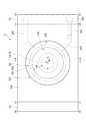
図1は、第一実施形態の波長可変干渉フィルター5の概略構成を示す平面図である。図2は、図2をA−A線で切断にした波長可変干渉フィルター5の概略構成を示す断面図である。
波長可変干渉フィルター5は、図1及び図2に示すように、第一基板51および第二基板52を備えている。これらの第一基板51及び第二基板52は、例えばシロキサンを主成分とするプラズマ重合膜等の接合膜53により接合されて、一体的に構成されている。
第一基板51には、第一ミラー54が設けられ、第二基板52には、第二ミラー55が設けられ、これらの第一ミラー54および第二ミラー55は、ミラーギャップGを介して対向配置されている。また、波長可変干渉フィルター5には、ミラーギャップGの寸法を変更する静電アクチュエーター56を備えている。
以下、各部の構成を詳細に説明する。
[First embodiment]
Hereinafter, the variable wavelength interference filter according to the first embodiment will be described.
FIG. 1 is a plan view showing a schematic configuration of a variable
The variable
The
Hereinafter, the configuration of each unit will be described in detail.
(第一基板の構成)
第一基板51は、第一実施形態において本発明の対向基板に相当する。第一基板51は、図2に示すように、第二基板52に対向する面に、例えばエッチングにより形成された電極配置溝511及びミラー設置部512を備える。この第一基板51は、例えば第二基板52に対して厚み寸法が大きく形成されており、静電アクチュエーター56により静電引力を作用させた際の第一基板51が抑制されている。
また、第一基板51の一端側(例えば、図1における辺C5−C6)は、第二基板52の一端側(辺C1−C2)よりも突出し、波長可変干渉フィルター5を例えばパッケージ筐体や基台等に固定する際の固定部として用いることができる。
(Configuration of the first substrate)
The
Further, one end side (for example, side C5-C6 in FIG. 1) of the
電極配置溝511は、第一基板51を基板厚み方向から見た平面視(以降、単に平面視と称する)において、所定のフィルター中心軸Oを中心とした略環状に形成されている。また、図示は省略するが、第一基板51には、電極配置溝511から辺C3−C4に向かって、電極配置溝511と同一深さ寸法の引出溝が延設されている。
The
そして、電極配置溝511の溝底面には、静電アクチュエーター56を構成する第一電極561が配置されている。
第一電極561は、電極配置溝511の溝底面のうち、後述する第二電極562に対向する領域に設けられている。この第一電極561は、例えば電極配置溝に沿った略環状に形成される。
また、第一電極561には、引出溝に沿って辺C3−C4側に延設される第一引出電極563(図1参照)が接続されている。この第一引出電極563は、引出溝において、第二基板52側に設けられた第一接続電極565に接続される。
なお、本実施形態では、1つの第一電極561が設けられる構成を示すが、例えば、フィルター中心軸Oを中心とした同心円となる2つ以上の電極が設けられる構成などとしてもよい。また、第一電極561の形状としては、例えば、一部に環内外を連通する切欠部が設けられる構成としてもよい。この場合、当該切欠部を通って、第一電極561から独立した他の電極(例えば第一ミラー54と接続される電極等)を設けることもできる。
A
The
The
In the present embodiment, a configuration in which one
ミラー設置部512は、平面視において、電極配置溝511の内側(フィルター中心軸O側)に設けられ、図2に示すように、第二基板52側に突出して形成されている。このミラー設置部512の突出先端面は平面であり、当該突出先端面に第一ミラー54が設けられている。
第一ミラー54は、例えばAg等の金属膜や、Ag合金等の合金膜、高屈折層(例えばTiO2)及び低屈折層(例えばSiO2)を積層した誘電体多層膜等を用いることができる。
The
For the
また、第一基板51の第二基板52に対向する面のうち、電極配置溝511、ミラー設置部512及び引出溝が形成されない面には第一接合部513が設けられる。第一接合部513は、接合膜53を介して第二基板52に接合される。
In addition, the
なお、本実施形態では、電極配置溝511よりもミラー設置部512が第二基板52側に位置する例を示すが、例えば、波長可変干渉フィルター5を透過させる光の波長域によっては、電極配置溝511がミラー設置部512より第二基板52側に位置する構成としてもよい。つまり、平面視における電極配置溝511の内側(フィルター中心軸O側)に凹部を形成し、当該凹部の底面に第一ミラー54を設けてもよい。
In the present embodiment, an example is shown in which the
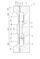
(第二基板の構成)
第二基板52は、本発明の基板に相当する。第二基板52は、第二基板52の一端側(辺C3−C4側)は、第一基板51の辺C7−C8よりも外側に突出し、電装部560を構成する。また、第二基板52の第一基板51に対向する面(第一面521)には、第二ミラー55及び第二電極562が設けられている。
そして、第二基板52の第一基板51とは反対側の面(第二面522)には、第一基板51側に凹状となる第一凹部523が設けられ、平面視において、第一凹部523の外側側には基板外周部524が設けられている。
(Configuration of second substrate)
The
A surface of the
第一凹部523は、第二基板52の第二面522に対してウェットエッチングを実施することで形成され、平面視で略円形となる凹部である。この第一凹部523は、フィルター中心軸Oを中心とした所定径寸法の底部525と、底部525の外側に設けられて基板外周部524に連続する湾曲部526とを備える。
ここで、図1に示すような平面視において、底部525のうち、第一ミラー54と重なる領域をミラー領域Amと称し、ミラー領域Amの外周縁から湾曲部526までの領域をダイアフラム領域Adと称する。
The
Here, in a plan view as shown in FIG. 1, a region of the bottom 525 that overlaps the
本実施形態では、第一凹部523における第一基板51とは反対側の表面のうち、底部525と重なる底面は、静電アクチュエーター56に電圧を印加していない状態で、ミラー領域Amからダイアフラム領域Adに亘って平坦な平面となる。すなわち、本実施形態では、ミラー領域Amとダイアフラム領域Adとが平面視において隣接している。
また、第一凹部523における第一基板51とは反対側の表面のうち、湾曲部526と重なる面は、底面525Aの外周縁から基板外周部524における第一基板51とは反対側の面(第二面522)までを連続する円弧状の曲面となる。
In the present embodiment, of the surface of the
Of the surface of the
第二基板52の第一面521には、平面視でミラー領域Amと重なる位置で、第一面521よりも第一基板51側に突出する突出部527を有する。この突出部527は、例えば第二基板52を形成するための母材の、第一基板51に対向させる一面のうち、当該突出部527以外の領域にドライエッチングを実施することで形成される。突出部527の突出先端面は、第一基板51のミラー設置部512の突出先端面と平行であり、当該突出部527の突出先端面に第二ミラー55が設けられる。
The
この突出部527の第一面521からの突出寸法は、底部525におけるダイアフラム領域Adの厚み寸法の2〜3倍である。底部525において、ミラー領域Amの厚み寸法は、ダイアフラム領域Adの厚み寸法の3〜4倍程度となる。この場合、ダイアフラム領域Adが第一基板51側に撓んだ際の応力によって、ミラー領域Amが撓む不都合を抑制でき、第二ミラー55の撓みを抑制できる。
また、突出部527の突出寸法は、第一凹部523の深さ寸法(第二面522から底面525Aまでの距離)よりも小さい。例えば、基板厚み寸法が500μmの第二基板52に対して、例えば350μmの深さ寸法で第一凹部523が形成されるのに対し、突出部527を形成する際のドライエッチングの深さ寸法は例えば100μmとなる。この場合、50μmの厚み寸法のダイアフラム領域Adに対して、突出部527の突出寸法が100μm、ミラー領域Amの厚み寸法が150μmとなる。
The projecting dimension of the projecting
Further, the projecting dimension of the projecting
本実施形態では、第二基板52の母材に上記ドライエッチングを実施した際に、エッチングされた部分により第一面521が構成される。そして、当該第一面521のうち、後述する第二凹部528が設けられる部分以外の面は、静電アクチュエーター56に電圧を印加していない状態で平坦な平面となる。
第一面521は、基板外周部524から、湾曲部526、ダイアフラム領域Adに亘って設けられる。第一面521のうち、基板外周部524を重なる領域で、かつ、第一基板51の第一接合部513に対向する部分は、第二接合部524Aを構成し、接合膜53を介して第一基板51の第一接合部513に接合される。
In the present embodiment, when the dry etching is performed on the base material of the
The
ところで、上記の例では、第二基板52の母材の第一基板51に対向させる面にドライエッチングを実施することで突出部527を形成した。この場合、異方性エッチングとなるので、突出部527の側面と第一面521との境界は、略直角に交差する角部となる。したがって、ミラー領域Amとダイアフラム領域Adとを略隣接させて配置することができる。しかしながら、ダイアフラム領域Adを第一基板51側に撓ませた際に、当該角部に応力が集中することで、クラックが発生する可能性がある。
したがって、突出部527を、第二基板52の母材の第一基板51に対向させる面にウェットエッチングを実施することで形成してもよい。この場合、突出部527の突出先端面から第一面521に亘って円弧状の湾曲面が形成され、上記のようなクラックの発生を抑制できる。
In the above example, the
Therefore, the protruding
第二ミラー55は、上述したように、突出部527の突出先端面に設けられる。突出先端面は、第一ミラー54が設けられるミラー設置部512の突出先端面と平行な平面であるため、第一ミラー54及び第二ミラー55も平行となる。
この第二ミラー55としては、上述した第一ミラー54と同一の構成の反射膜を用いることができる。
The
As the
図3は、第一凹部523のダイアフラム領域Adの一部を拡大した断面図である。
本実施形態では、第二基板52の第一面521には、図3に示すように、複数の第二凹部528(マイクロダイアフラム)が、例えばマトリクス状に設けられている。具体的には、第二凹部528は、第一面521のうち、第一凹部523と重なる領域内で、かつ、ミラー領域Am以外の領域に設けられている。
なお、本実施形態では、第二凹部528がダイアフラム領域Adと湾曲部526とに重なる領域内に設けられる例を示すが、ダイアフラム領域Adと重なる領域内のみに設けられる構成としてもよく、湾曲部526と重なる領域のみに設けられる構成としてもよい。
FIG. 3 is an enlarged cross-sectional view of a part of the diaphragm region Ad of the
In the present embodiment, on the
In the present embodiment, an example is shown in which the
この第二凹部528は、略半球状の凹部であり、平面視における径寸法は、第一凹部523の径寸法に対して十分に小さい。また、第二凹部528の深さ寸法(半径寸法)は、図3に示すように、第一凹部523の底部525の厚み寸法(第二ミラー55の法線方向に沿う寸法)よりも小さい。
このような第二凹部528を設けることで、当該第二凹部528での厚み寸法が小さくなるので、ダイアフラム領域Adが第一基板51側に撓みやすくなる。
The
By providing such a
そして、第二基板52の第一面521には、ミラー領域Am以外の領域で、かつ、少なくともダイアフラム領域Adと重なる位置に、第一電極561に対向する略環状の第二電極562が設けられている。
本実施形態では、第二電極562は、底部525のダイアフラム領域Adから湾曲部526に亘って設けられている。また、第二凹部528と重なる部分では、第二電極562は第二凹部528の凹内周面に沿って形成されている。すなわち、第二電極562の第二凹部528と重なる部分は、第二凹部528の凹曲面と略同一形状の凹状(略半球状)となる。
The
In the present embodiment, the
なお、ここでは、ダイアフラム領域Adと重なる領域から湾曲部526と重なる領域に亘って第二電極562が設けられる例を示すが、例えば、ダイアフラム領域Adと重なる領域のみに第二電極562が設けられる構成としてもよい。
また、第二電極562としては、第一電極561と同様、例えば、フィルター中心軸Oを中心とした同心円となる2つ以上の電極が設けられる構成などとしてもよく、一部に環内外を連通する切欠部が設けられる構成としてもよい。
Here, an example is shown in which the
Further, as the
そして、第二基板52には、第二電極562の外周縁から第一基板51の引出溝に対向する領域を通り、電装部560まで延設される第二引出電極564(図1参照)を備えている。
さらに、第二基板52には、第一基板51の引出溝に対向する領域から電装部560に亘って設けられる第一接続電極565を備えている。この第一接続電極565は、第一基板51の引出溝に設けられる第一引出電極563と、例えばバンプ電極を介して接続される。
The
Furthermore, the
以上のような波長可変干渉フィルター5では、第二引出電極564と第一接続電極565とを、波長可変干渉フィルター5を制御する制御回路(ドライバー回路)に接続し、当該制御回路により、静電アクチュエーター56を構成する第一電極561及び第二電極562の間に印加する電圧を制御する。これにより、第一電極561及び第二電極562の間で静電引力が作用し、第一凹部523のダイアフラム領域Adが第一基板51側に変位して、ミラーギャップGの寸法を変更することが可能となる。
この際、第二電極562が、第一面521及び第二凹部528の凹内周面に沿って形成される。このような構成では、第一面521に沿って平坦な第二電極が形成される場合に比べて、第二電極562の表面積を増大でき、静電アクチュエーター56に所定電圧を印加した際の第二電極562に保持される電荷量も増大する。よって、静電アクチュエーター56に所定電圧を印加した際に発生する静電引力も増大する。
In the wavelength
At this time, the
[波長可変干渉フィルターの平面寸法]
次に、上記のような本実施形態の波長可変干渉フィルター5の基板厚み方向に直交する方向の寸法(平面寸法)について説明する。
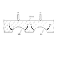
図4は、従来の波長可変干渉フィルター5fと、本実施形態の波長可変干渉フィルター5との寸法を比較した図である。なお、図4では、説明の簡略化のため、第二基板52の一部のみを表示する。
図4において、上段は、従来の波長可変干渉フィルター5fの第二基板52fを示している。従来の波長可変干渉フィルター5fでは、第二基板52fは、フィルター中心軸Oを中心とした可動部520fを備え、可動部520fの周囲に環状の凹部523fが形成される。可動部520fにミラー領域Amが設けられ、凹部523fの底部525fがダイアフラム領域Adを構成する。このような構成では、凹部523fの底部525fと可動部520fとの間、及び、底部525fと基板外周部524fとの間のそれぞれに円弧面を有する湾曲部526fが設けられる。
このため、波長可変干渉フィルター5fの基板厚み方向に直交する方向の寸法L1(平面寸法)は、最小でも、ミラー領域Amの寸法Lmと、2つのダイアフラム領域Adの寸法Ldと、2つの基板外周部524fの寸法Loと、4つの湾曲部526fの寸法LRとを合計した分(つまり、L1=Lm+2Ld+2Lo+4LR)だけ必要となる。
[Plane dimensions of tunable interference filter]
Next, the dimension (plane dimension) in the direction orthogonal to the substrate thickness direction of the wavelength
FIG. 4 is a diagram comparing the dimensions of the conventional
In FIG. 4, the upper part shows the
For this reason, the dimension L1 (planar dimension) in the direction orthogonal to the substrate thickness direction of the wavelength
図4の中段に示す図は、本実施形態の波長可変干渉フィルター5の第二基板52を示している。図4に示すように、波長可変干渉フィルター5は、従来の波長可変干渉フィルター5fと同じ寸法のミラー領域Am、ダイアフラム領域Ad、基板外周部524を有するが、ミラー領域Amとダイアフラム領域Adとの間に湾曲部526が設けられない。したがって、本実施形態では、波長可変干渉フィルター5の基板厚み方向に直交する方向の寸法L2は、L2=Lm+2Ld+2Lo+2LRとなり、2つの湾曲部526に相当する寸法(2LR)だけ、従来の波長可変干渉フィルター5fよりも小さくなる。
4 shows the
図4の下段は、突出部527をウェットエッチングにより形成した場合の、波長可変干渉フィルター5Aである。突出部527をウェットエッチングにより形成する場合、突出部527と第一面521との間に湾曲面が形成され、ミラー領域Amとダイアフラム領域Adとの間にも湾曲部526Aが形成される。
しかしながら、上述したように、突出部527の突出寸法(ウェットエッチング時のエッチング深さ)は、第一凹部523の深さ寸法に比べて小さい。よって、図4の下段に示すように、湾曲部526Aの幅寸法LR2は、従来のミラー領域Amf及びダイアフラム領域Adfの間の湾曲部526fの幅寸法LRに比べて十分に小さくなる。このため、この場合でも、従来の波長可変干渉フィルター5fに比べて、波長可変干渉フィルター5Aの平面寸法が小さくなる。
The lower part of FIG. 4 shows the variable
However, as described above, the protrusion dimension of the protrusion 527 (etching depth during wet etching) is smaller than the depth dimension of the
[波長可変干渉フィルター5の製造方法]
次に、上述したような波長可変干渉フィルター5の製造方法について説明する。
図5は、本実施形態における波長可変干渉フィルター5の製造方法におけるフローチャートである。
波長可変干渉フィルター5の製造では、図5に示すように、第一基板形成ステップS1、第一電極形成ステップS2、第一ミラー形成ステップS3、第二基板形成ステップS4、第二電極形成ステップS5、第二ミラー形成ステップS6、及び接合ステップS7により形成される。なお、第一基板形成ステップS1〜第一ミラー形成ステップS3の後に、第二基板形成ステップS4〜第二ミラー形成ステップS6を実施する例を示すが、例えば、第二基板形成ステップS4〜第二ミラー形成ステップS6の後に、第一基板形成ステップS1〜第一ミラー形成ステップS3を実施してもよい。
[Method for Manufacturing Wavelength Variable Interference Filter 5]
Next, a manufacturing method of the wavelength
FIG. 5 is a flowchart in the manufacturing method of the wavelength
In the manufacture of the variable
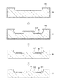
図6は、第一基板形成ステップS1から第一ミラー形成ステップS3の各ステップにおける第一基板51(第一ガラス基板M1)の概略を示す図である。
なお、ここでは、第一基板51及び第二基板52として、ガラス基板を用いる例を説明する。
FIG. 6 is a diagram schematically showing the first substrate 51 (first glass substrate M1) in each step from the first substrate forming step S1 to the first mirror forming step S3.
Here, an example in which glass substrates are used as the
(第一基板形成ステップ)
第一基板形成ステップS1では、第一基板51の母材となる第一ガラス基板M1の表面に対して、レジストR1を形成し、フォトリソグラフィー法によりレジストR1をパターニングして電極配置溝511及び引出溝の底面及びミラー設置部512の形成領域を開口させる。この後、図6の1番目に示すように、ウェットエッチングを実施して、ミラー設置部512の突出先端面の深さ寸法まで第一ガラス基板M1の一面を掘り下げる。ガラス基板に対するウェットエッチングでは、例えば、バッファードフッ酸(例えば、NH4HF2(20.2重量%)、NH4F(21.2重量%)の混合水溶液)をエッチング液とする。ガラス基板に対して、算術平均粗さRaが1nm未満となる凹溝をエッチングにより形成する場合、例えばエッチング処理時の温度を30度とし、例えば10分程度のエッチング処理と、乾燥処理と、を交互に複数回実施する。
(First substrate formation step)
In the first substrate forming step S1, a resist R1 is formed on the surface of the first glass substrate M1 which is a base material of the
この後、ミラー設置部512を覆うレジストR2を形成する。例えば、レジストR1を除去した後、第一ガラス基板M1の表面にレジストR2を形成して、フォトリソグラフィー法を用いたパターニングにより電極配置溝511の底面部を開口させる。この後、例えばバッファードフッ酸を用いたウェットエッチングを実施して、図6の2番目に示すように、電極配置溝511の底面の深さ寸法まで第一ガラス基板M1の一面を掘り下げる。この後、レジストR2を除去する。
Thereafter, a resist R2 that covers the
(第一電極形成ステップ)
次に、第一電極形成ステップS2を実施して、図6の3番目に示すように、第一電極561及び第一引出電極563(図6では図示略)を形成する。また、第一電極形成ステップS2では、第一引出電極563と第一接続電極565とを接続するためのバンプ電極を形成する。
具体的には、引出溝の一部で、第一引出電極563と第一接続電極565とを接続させる位置に、引出溝の底面から第二基板52側に向かって立ち上がるバンプ部(図示略)を形成する。このバンプ部としては、例えば、Ti薄膜等の形成素材を成膜した後、エッチングによりバンプ部以外の領域を除去してもよく、例えば、第一基板形成ステップS1の実施時にバンプ部を形成しておいてもよい。この後、第一電極561及び第一引出電極563を形成し、その際に、第一引出電極563をバンプ部の上面まで形成する。
(First electrode formation step)
Next, a first electrode formation step S2 is performed to form a
Specifically, a bump portion (not shown) that rises from the bottom surface of the extraction groove toward the
第一電極561及び第一引出電極563の形成では、例えば、第一ガラス基板M1に電極材料を、蒸着法やスパッタリング法等を用いて成膜する。この電極材料としては、例えばITO膜、TiW膜及びAu膜の積層体、Cr膜及びAu膜の積層体等を用いることができ、その他、第一基板51の素材(本実施形態ではガラス)と密着性が良好で、かつ導電性を有する各種膜材を用いることができる。
そして、第一ガラス基板M1に、例えば、第一電極561及び第一引出電極563の形成位置が開口したレジストパターンを形成して、ウェットエッチングを実施することで、第一電極561及び第一引出電極563を形成する。
In the formation of the
Then, for example, by forming a resist pattern in which the formation positions of the
(第一ミラー形成ステップ)
第一ミラー形成ステップS3では、図6の4番目に示すように第一ミラー54を形成する。この第一ミラー形成ステップS3では、例えばスパッタリング法等により第一ミラー54を第一ガラス基板M1上に形成し、第一ミラー54の形成位置が開口したレジストパターンを形成して、ウェットエッチングを実施する。なお、第一ミラー54上に、さらに、保護膜を形成してよい。
以上により第一基板51が形成される。
(First mirror formation step)
In the first mirror forming step S3, the
Thus, the
(第二基板形成ステップ)
図7は、第二基板形成ステップS4から第二ミラー形成ステップS6の各ステップにおける第二基板52(第二ガラス基板M2)の概略を示す図である。
第二基板形成ステップS4は、本発明の凹部形成ステップに相当する。なお、本実施形態では、第二ガラス基板M2の基板表面は、例えば算術平均粗さRaが1nm未満となるように予め表面処理されているものとする。この場合、第二ガラス基板M2の一部を第二面522、突出部527の突出先端面とすることができる。
第二基板形成ステップS4では、まず、第二基板52の母材となる第二ガラス基板M2の表面に対して、レジストR3を形成し、フォトリソグラフィー法により、第二ガラス基板M2の一面(第二面522に相当する上面M22)に、第一凹部523の底部525に相当する部分が開口するよう、レジストR3をパターニングする。
(Second substrate formation step)
FIG. 7 is a diagram showing an outline of the second substrate 52 (second glass substrate M2) in each step from the second substrate forming step S4 to the second mirror forming step S6.
The second substrate forming step S4 corresponds to the recess forming step of the present invention. In the present embodiment, it is assumed that the substrate surface of the second glass substrate M2 is surface-treated in advance so that, for example, the arithmetic average roughness Ra is less than 1 nm. In this case, a part of the second glass substrate M2 can be the
In the second substrate forming step S4, first, a resist R3 is formed on the surface of the second glass substrate M2 which is a base material of the
この後、ウェットエッチングを実施して、所定寸法の深さ寸法まで第二ガラス基板M2の上面M22を掘り下げて、第一凹部523を形成する。このウェットエッチングでは、例えば、バッファードフッ酸をエッチング液としたエッチング処理を例示できる。このようなウェットエッチングでは、レジストR3の開口部分に対して、エッチング時間に応じて、第二ガラス基板M2の一面が均一に掘り下げられる。また、ウェットエッチングでは、レジストの下部にもエッチング液が回り込んで、エッチングが進行する(所謂サイドエッチング)。このため、図7の1番目に示すように、第一凹部523は、凹内部に面する平面状の底面を有する底部525と、当該底面から第二面522まで連続する円弧面を有する湾曲部526とを有する形状となる。
Thereafter, wet etching is performed to dig up the upper surface M22 of the second glass substrate M2 to a predetermined depth, thereby forming a
次に、第二ガラス基板M2の上面M22とは反対側の下面M21のうち、突出部527の形成位置を覆うレジストR4を、例えばフォトリソグラフィー等によって形成する。
この後、第二ガラス基板M2の下面M21に対して、ドライエッチングを実施し、突出部527の突出寸法分だけ下面M21を掘り下げる。このドライエッチングでは、例えば、ICP(Inductive Coupled Plasma)エッチング装置を用いたRIE(Reactive Ion Etching)により、レジストR4が形成されていない範囲の下面M21をエッチングする。この際、上述したように、ミラー領域Amの厚み寸法が、ダイアフラム領域Adの厚み寸法の3〜4倍となるように、エッチング深さを制御する。これにより、図7の2番目に示すように、突出部527及び第一面521が形成される。
Next, a resist R4 that covers the position where the protruding
Thereafter, dry etching is performed on the lower surface M21 of the second glass substrate M2, and the lower surface M21 is dug down by the protruding dimension of the protruding
この後、レジストR4を除去した後、第二ガラス基板M2の表面に対して、レジストR5を形成する。また、第一面521のうち、ダイアフラム領域Ad及び湾曲部526と重なる領域で、第二凹部528の形成位置が開口するように、レジストR5をパターニングする。そして、第二ガラス基板M2に対して、例えばバッファードフッ酸を用いたウェットエッチングを実施することで、図7の3番目に示すように、第二凹部528を形成する。
Thereafter, after removing the resist R4, a resist R5 is formed on the surface of the second glass substrate M2. Further, the resist R5 is patterned so that the formation position of the
(第二電極形成ステップ)
第二電極形成ステップS5では、図7の4番目に示すように、第二電極562、第二引出電極564、及び第一接続電極565を形成する。
この第二電極形成ステップS5では、第一電極形成ステップS2と同様に、例えば、第二ガラス基板M2に形成された第一面521に電極材料を、蒸着法やスパッタリング法等を用いて均一に成膜する。これにより、第二凹部528に対して、凹内周面に沿って電極材料が形成される。つまり、第二凹部528に対して、表面形状が凹状となるように電極材料が製膜される。なお、電極材料は、第一電極561と同様、例えばITO膜、TiW膜及びAu膜の積層体、Cr膜及びAu膜の積層体等を用いることができる。そして、第二ガラス基板M2に、第二電極562、第二引出電極564、及び第一接続電極565の形成位置が開口したレジストパターンを形成して、ウェットエッチングを実施することで、第二電極562、第二引出電極564、及び第一接続電極565を形成する。
(Second electrode formation step)
In the second electrode formation step S5, as shown in the fourth part of FIG. 7, the
In the second electrode formation step S5, as in the first electrode formation step S2, for example, the electrode material is uniformly applied to the
(第二ミラー形成ステップ)
第二ミラー形成ステップS6では、図7の5番目に示すように第二ミラー55を形成する。この第二ミラー形成ステップS6では、第一ミラー形成ステップS3と同様、例えばスパッタリング法等により第二ミラー55を第二ガラス基板M2上に形成し、第二ミラー55の形成位置が開口したレジストパターンを形成して、ウェットエッチングを実施する。なお、第二ミラー55上に、さらに、保護膜を形成してよい。
以上により第二基板52が形成される。
(Second mirror forming step)
In the second mirror forming step S6, the
Thus, the
(接合ステップ)
以上の後、接合ステップS7を実施する。接合ステップS7では、第一基板51の第一接合部513と、第二基板52の第二接合部524Aとに、接合膜53を形成する。接合膜53としては、例えばポリオルガノシロキサンを主成分としたプラズマ重合膜を用いることができる。この場合、例えばプラズマCVD法等により接合膜53(プラズマ重合膜)の表面に対して、O2プラズマ処理又はUV処理を行い、表面を活性化させる。O2プラズマ処理の場合は、例えば、O2流量1.8×10⁻³(m3/h)、圧力27Pa、RFパワー200Wの条件で30秒間実施する。また、UV処理の場合は、UV光源としてエキシマUV(波長172nm)を用いて3分間処理する。そして、第一基板51及び第二基板52のアライメント調整を行い、表面が活性化されたプラズマ重合膜を重ね合せ、接合部分に例えば98(N)の荷重を10分間かける。これにより、第一基板51及び第二基板52同士が接合される。この際、第一引出電極563と、第一接続電極565とが、バンプ部で接続される。
(Joining step)
After the above, the joining step S7 is performed. In the bonding step S7, the
なお、接合膜53としては、これに限定されず、例えばAu等の金属膜を形成し、金属膜同士を接触させて荷重をかけることで金属結合させてもよく、その他、エポキシ樹脂等を用いた接着剤により第一基板51及び第二基板52を接合してもよい。
The
[第一実施形態の作用効果]
本実施形態では、第一ミラー54に対向する第二ミラー55を有する第二基板52において、第一ミラー54とは反対側となる第二面522から第一ミラー54側に向かって凹状となる第一凹部523が設けられる。この第一凹部523は、底部525と底部525の外側に設けられる湾曲部526とにより構成され、底部525は、第一ミラー54及び第二ミラー55と重なり合うミラー領域Amと、ミラー領域Amを第一ミラー54側に変位させるダイアフラム領域Adとを備える。
このような構成では、ミラー領域Am及びダイアフラム領域Adの間に湾曲面が形成されないため、図4に示すような従来の波長可変干渉フィルター5fに比べ、波長可変干渉フィルター5の平面寸法を小さくでき、小型の波長可変干渉フィルター5が得られる。
[Operational effects of the first embodiment]
In the present embodiment, in the
In such a configuration, since a curved surface is not formed between the mirror region Am and the diaphragm region Ad, the planar size of the wavelength
本実施形態では、第一凹部523の底部525のうちミラー領域Amには、第一面521から第一ミラー54側に突出する突出部527が設けられており、この突出部527の突出先端面に第二ミラー55が設けられている。
このため、ミラー領域Amは、突出部527の突出寸法分だけ、ダイアフラム領域Adよりも厚み寸法が大きくなる。よって、ミラー領域Amがダイアフラム領域Adよりも撓みにくくなり、静電アクチュエーター56を駆動させた際の第二ミラー55の撓みを抑制できる。
In the present embodiment, the mirror region Am of the bottom 525 of the
For this reason, the mirror region Am has a thickness dimension larger than that of the diaphragm region Ad by the projecting dimension of the projecting
本実施形態では、第二基板52の第一面521で、第一凹部523と重なる領域のうち、ミラー領域Am以外の領域(本実施形態では、ダイアフラム領域Ad及び湾曲部526)に、第二凹部528が設けられている。
このような構成では、第二凹部528の厚み寸法が、第二凹部528が設けられていないダイアフラム領域Adや湾曲部526の他の領域の厚み寸法よりも小さくなる。よって、第二凹部528の形成位置において、ダイアフラム領域Adを第一ミラー54側に撓ませやすくなる。これにより、第二ミラー55を第一ミラー54側に引っ張る応力が作用した際に、ミラー領域Amの撓みを抑制できる。
In the present embodiment, in the
In such a configuration, the thickness dimension of the
ここで、ダイアフラム領域Adは、ミラーギャップGを変更する際に、大きく撓む領域であり、上記のような第二凹部528を設けることで、第二ミラー55を所定量変位させる際の静電アクチュエーター56への駆動電圧を低減でき、省電力化を図れる。
また、湾曲部526は、ダイアフラム領域Adに比べて静電アクチュエーター56を駆動させた際の変形量が小さいが、この湾曲部526に対して第二凹部528が設けられることで、当該湾曲部526の変形量を増やすことができる。
Here, the diaphragm region Ad is a region that greatly bends when the mirror gap G is changed. By providing the
Further, the bending
そして、本実施形態では、第二電極562が、第二基板52の第一面521で、第二凹部528が設けられる領域内に形成されている。
つまり、第二電極562が、第二凹部528の凹内周面に沿って形成される。これにより、例えば第二凹部528が設けられていない平坦な第一面521に第二電極562を設ける場合に比べて、第二電極562の表面積を大きくできる。このため、静電アクチュエーター56に所定電圧を印加した際に、第二電極562にて保持可能な電荷量が増大し、小さい駆動電圧で大きい静電引力を作用させることができる。よって、ミラーギャップを所定寸法だけ変更するために必要な駆動電圧を小さくできる。
In the present embodiment, the
That is, the
[第二実施形態]
次に、第二実施形態について説明する。
上記第一実施形態では、第二基板52の第一基板51に対向する第一面521に第二凹部528(マイクロダイアフラム)を設ける例を示した。これに対して、第二実施形態では、マイクロダイアフラムが設けられる位置が第一実施形態と相違する。
図8は、第二実施形態の波長可変干渉フィルター5Bの概略構成を示す断面図である。なお、以降の説明にあたり、既に説明した事項については同一符号を付し、その説明を省略又は簡略化する。
[Second Embodiment]
Next, a second embodiment will be described.
In the first embodiment, the example in which the second recess 528 (micro diaphragm) is provided on the
FIG. 8 is a cross-sectional view showing a schematic configuration of a wavelength
本実施形態では、図8に示すように、第一基板51の構成は、第一実施形態と同様であるので、ここでの説明は省略する。
本実施形態の波長可変干渉フィルター5Bでは、第二基板52Bは、図8に示すように、第一実施形態と同様に、第一基板51とは反対側の第二面522にウェットエッチングを実施することで形成される第一凹部523Bが設けられている。
そして、この第一凹部523Bの凹内周面で、ダイアフラム領域Ad及び湾曲部526と重なる位置に、複数の第三凹部528Bが設けられている。
In the present embodiment, as shown in FIG. 8, the configuration of the
In the wavelength
A plurality of
[第二実施形態の作用効果]
図9は、第一実施形態におけるダイアフラム領域Adにおいて、第二凹部528に作用する力を模式的に示す図であり、図10は、第二実施形態におけるダイアフラム領域Adにおいて、第三凹部528Bに作用する力を模式的に示す図である。
第一実施形態では、第二基板52の第一面521に第二凹部528が設けられている。この場合、静電アクチュエーター56を駆動させてダイアフラム領域Adを変形させると、第二凹部528の位置の厚み寸法が、第二凹部528が設けられていない部分の厚み寸法よりも小さくなるので、ダイアフラム領域Adを撓みやすくすることができる。しかしながら、図9に示すように、ダイアフラム領域Adを撓ませる方向に応力P1が作用すると、第二凹部528の円弧状の内周面において、第一基板51から離れる方向にモーメント力P2が作用する。
[Operational effects of the second embodiment]
FIG. 9 is a diagram schematically showing the force acting on the
In the first embodiment, a
これに対して、第二実施形態では、図10に示すように、ダイアフラム領域Adを撓ませる方向に応力P1が作用すると、第三凹部528Bの底面部を第一基板51側に沈み込ませるように、つまり、第一基板51に向かってモーメント力P3が作用する。
したがって、応力P1とモーメント力P3との方向がどちらも第一基板51に向かう方向となり、ダイアフラム領域Adをより撓ませやすくできる。
On the other hand, in the second embodiment, as shown in FIG. 10, when the stress P1 is applied in the direction in which the diaphragm region Ad is bent, the bottom surface portion of the
Therefore, the directions of the stress P1 and the moment force P3 are both directions toward the
[第三実施形態]
次に、第三実施形態として、上記第一実施形態の波長可変干渉フィルター5を備えた光学デバイスについて説明する。
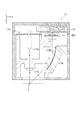
図11は、第三実施形態における光学デバイス600の概略構成を示す断面図である。
図11に示すように、光学デバイス600は、筐体610と、筐体610の内部に収納される波長可変干渉フィルター5を備えている。なお、ここでは、第一実施形態に示す波長可変干渉フィルター5を筐体610内に収納する例を示すが、第二実施形態の波長可変干渉フィルター5Bが収納されてもよい。
[Third embodiment]
Next, as a third embodiment, an optical device including the wavelength
FIG. 11 is a cross-sectional view illustrating a schematic configuration of an
As shown in FIG. 11, the
筐体610は、図11に示すように、ベース620と、リッド630と、を備えている。これらのベース620及びリッド630が接合されることで、内部に収容空間が形成され、この収容空間内に波長可変干渉フィルター5が収納される。
The
(ベースの構成)
ベース620は、例えばセラミック等により構成されている。このベース620は、台座部621と、側壁部622と、を備える。
台座部621は、フィルター平面視において例えば矩形状の外形を有する平板状に構成されており、この台座部621の外周部から筒状の側壁部622がリッド630に向かって立ち上がる。
(Base configuration)
The
The
台座部621は、厚み方向に貫通する開口部623を備えている。この開口部623は、台座部621に波長可変干渉フィルター5を収容した状態で、台座部621を厚み方向から見た平面視において、第一ミラー54及び第二ミラー55と重なる領域を含むように設けられている。
また、台座部621のリッド630とは反対側の面(ベース外側面621B)には、開口部623を覆うガラス部材627が接合されている。台座部621とガラス部材627との接合は、例えば、ガラス原料を高温で熔解し、急冷したガラスのかけらであるガラスフリット(低融点ガラス)を用いた低融点ガラス接合、エポキシ樹脂等による接着などを利用できる。本実施形態では、収容空間内が減圧下に維持された状態で気密に維持する。したがって、台座部621及びガラス部材627は、低融点ガラス接合を用いて接合されることが好ましい。
The
Further, a
また、台座部621のリッド630に対向する内面(ベース内側面621A)には、波長可変干渉フィルター5の第一接続電極565や第二引出電極564に接続される内側端子部624が設けられている。内側端子部624と、第一接続電極565及び第二引出電極564とは、例えばAu等のワイヤーを用いたワイヤーボンディングにより接続される。なお、本実施形態では、ワイヤーボンディングを例示するが、例えば、FPC(Flexible Printed Circuits)等を用いてもよい。
また、台座部621は、内側端子部624が設けられる位置に、貫通孔625が形成されている。内側端子部624は、貫通孔625を介して、台座部621のベース外側面621Bに設けられた外側端子部626に接続されている。
Further, an
The
側壁部622は、台座部621の縁部から立ち上がり、ベース内側面621Aの周囲を囲って設けられる側壁部622のリッド630に対向する面(端面622A)は、例えばベース内側面621Aに平行な平坦面となる。
The
そして、ベース620には、例えば接着剤等の固定材64を用いて、波長可変干渉フィルター5が固定される。この際、波長可変干渉フィルター5は、台座部621に対して固定されていてもよく、側壁部622に対して固定されていてもよい。固定材64を設ける位置としては、複数個所であってもよいが、固定材64の応力が波長可変干渉フィルター5に伝達するのを抑制するべく、1か所で波長可変干渉フィルター5を固定することが好ましい。
The variable
(リッドの構成)
リッド630は、平面視において矩形状の外形を有する透明部材であり、例えばガラス等により構成される。
リッド630は、図11に示すように、ベース620の側壁部622に接合されている。この接合方法としては、例えば、低融点ガラスを用いた接合等が例示できる。
(Lid composition)
The
As shown in FIG. 11, the
[第三実施形態の作用効果]
上述したような本実施形態の光学デバイス600では、筐体610により波長可変干渉フィルター5が保護されているため、外的要因による波長可変干渉フィルター5の破損を防止できる。
また、上述したように、波長可変干渉フィルター5は、1つの第一凹部523の底部525内にミラー領域Amとダイアフラム領域Adとが設けられる構成であって、平面寸法を小型化できる。したがって、このような波長可変干渉フィルター5を収納するための筐体610も小型化することができるので、光学デバイス600の小型化を図ることができる。
[Operational effects of the third embodiment]
In the
Further, as described above, the variable
[第四実施形態]
次に、第四実施形態として、上記第一実施形態や第二実施形態の波長可変干渉フィルター5,5A,5B又は第三実施形態の光学デバイス600を備えた電子機器の一例として、印刷装置(プリンター)について説明する。
[Fourth embodiment]
Next, as a fourth embodiment, as an example of an electronic apparatus including the wavelength
[プリンターの概略構成]
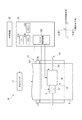
図12は、第四実施形態のプリンター10の外観の構成例を示す図である。図13は、本実施形態のプリンター10の概略構成を示すブロック図である。
図12に示すように、プリンター10は、供給ユニット11、搬送ユニット12と、キャリッジ13と、キャリッジ移動ユニット14と、制御ユニット15(図13参照)と、を備えている。このプリンター10は、例えばパーソナルコンピューター等の外部機器20から入力された印刷データに基づいて、各ユニット11,12,14及びキャリッジ13を制御し、媒体A上に画像を印刷する。また、本実施形態のプリンター10は、予め設定された較正用印刷データに基づいて媒体A上の所定位置に測色用のカラーパッチを形成し、かつ当該カラーパッチに対する分光測定を行う。これにより、プリンター10は、カラーパッチに対する実測値と、較正用印刷データとを比較して、印刷されたカラーに色ずれがあるか否か判定し、色ずれがある場合は、実測値に基づいて色補正を行う。
以下、プリンター10の各構成について具体的に説明する。
[Schematic configuration of printer]
FIG. 12 is a diagram illustrating an external configuration example of the
As shown in FIG. 12, the
Hereinafter, each configuration of the
供給ユニット11は、画像形成対象となる媒体Aを、画像形成位置に供給するユニットである。この供給ユニット11は、例えば媒体Aが巻装されたロール体111(図12参照)、ロール駆動モーター(図示略)、及びロール駆動輪列(図示略)等を備える。そして、制御ユニット15からの指令に基づいて、ロール駆動モーターが回転駆動され、ロール駆動モーターの回転力がロール駆動輪列を介してロール体111に伝達される。これにより、ロール体111が回転し、ロール体111に巻装された紙面がY方向(副走査方向)における下流側(+Y方向)に供給される。
なお、本実施形態では、ロール体111に巻装された紙面を供給する例を示すがこれに限定されない。例えば、トレイ等に積載された紙面等の媒体Aをローラー等によって例えば1枚ずつ供給する等、如何なる供給方法によって媒体Aが供給されてもよい。
The
In the present embodiment, an example in which the paper surface wound around the
搬送ユニット12は、供給ユニット11から供給された媒体Aを、Y方向に沿って搬送する。この搬送ユニット12は、搬送ローラー121と、搬送ローラー121と媒体Aを挟んで配置され、搬送ローラー121に従動する従動ローラー(図示略)と、プラテン122と、を含んで構成されている。
搬送ローラー121は、図示略の搬送モーターからの駆動力が伝達され、制御ユニット15の制御により搬送モーターが駆動されると、その回転力により回転駆動されて、従動ローラーとの間に媒体Aを挟み込んだ状態でY方向に沿って搬送する。また、搬送ローラー121のY方向の下流側(+Y側)には、キャリッジ13に対向するプラテン122が設けられている。
The
The
キャリッジ13は、媒体Aに対して画像を印刷する印刷部16と、媒体A上の所定の測定位置T(図13参照)の分光測定を行う分光器17と、を備えている。
このキャリッジ13は、キャリッジ移動ユニット14によって、Y方向と交差する主走査方向に沿って移動可能に設けられている。
また、キャリッジ13は、フレキシブル回路131により制御ユニット15に接続され、制御ユニット15からの指令に基づいて、印刷部16による印刷処理及び、分光器17による分光測定処理を実施する。
なお、キャリッジ13の詳細な構成については後述する。
The
The
Further, the
The detailed configuration of the
キャリッジ移動ユニット14は、本発明における移動機構を構成し、制御ユニット15からの指令に基づいて、キャリッジ13をX方向に沿って往復移動させる。
このキャリッジ移動ユニット14は、例えば、キャリッジガイド軸141と、キャリッジモーター142と、タイミングベルト143と、を含んで構成されている。
キャリッジガイド軸141は、X方向に沿って配置され、両端部がプリンター10の例えば筐体に固定されている。キャリッジモーター142は、タイミングベルト143を駆動させる。タイミングベルト143は、キャリッジガイド軸141と略平行に支持され、キャリッジ13の一部が固定されている。そして、制御ユニット15の指令に基づいてキャリッジモーター142が駆動されると、タイミングベルト143が正逆走行され、タイミングベルト143に固定されたキャリッジ13がキャリッジガイド軸141にガイドされて往復移動する。
The
The
The
次に、キャリッジ13に設けられる印刷部16及び分光器17の構成について、図面に基づいて説明する。
[印刷部16の構成]
印刷部16は、媒体Aと対向する部分に、インクを個別に媒体A上に吐出して、媒体A上に画像を形成する。
この印刷部16は、複数色のインクに対応したインクカートリッジ161が着脱自在に装着されており、各インクカートリッジ161からインクタンク(図示略)にチューブ(図示略)を介してインクが供給される。また、印刷部16の下面(媒体Aに対向する位置)には、インク滴を吐出するノズル(図示略)が、各色に対応して設けられている。これらのノズルには、例えばピエゾ素子が配置されており、ピエゾ素子を駆動させることで、インクタンクから供給されたインク滴が吐出されて媒体Aに着弾し、ドットが形成される。
Next, the configuration of the
[Configuration of Printing Unit 16]
The
The
[分光器の構成]
図14は、分光器17の概略構成を示す断面図である。
分光器17は、本発明における光学モジュールであり、図14に示すように、光源部171と、光学デバイス600、受光部173と、導光部174と、を備えている。
この分光器17は、光源部171から媒体A上の測定位置Tに照明光を照射し、測定位置Tで反射された光成分を、導光部174により光学デバイス600に入射させる。そして、光学デバイス600は、第三実施形態の構成を有し、反射光から所定波長の光を出射(透過)させて、受光部173により受光させる。また、光学デバイス600は、制御ユニット15の制御に基づいて、透過波長を選択可能であり、可視光における各波長の光の光量を測定することで、媒体A上の測定位置Tの分光測定が可能となる。
[Configuration of spectrometer]
FIG. 14 is a cross-sectional view showing a schematic configuration of the
The
The
[光源部の構成]
光源部171は、光源171Aと、集光部171Bとを備える。この光源部171は、光源171Aから出射された光を媒体Aの測定位置T内に、媒体Aの表面に対する法線方向から照射する。
光源171Aとしては、可視光域における各波長の光を出射可能な光源が好ましい。このような光源171Aとして、例えばハロゲンランプやキセノンランプ、白色LED等を例示でき、特に、キャリッジ13内の限られたスペース内で容易に設置可能な白色LEDが好ましい。集光部171Bは、例えば集光レンズ等により構成され、光源171Aからの光を測定位置Tに集光させる。なお、図14においては、集光部171Bでは、1つのレンズ(集光レンズ)のみを表示するが、複数のレンズを組み合わせて構成されていてもよい。
[Configuration of light source section]
The
The
[受光部及び導光光学系の構成]
受光部173は、波長可変干渉フィルター5の光軸上に配置され、当該波長可変干渉フィルター5を透過した光を受光する。そして、受光部173は、制御ユニット15の制御に基づいて、受光量に応じた検出信号(電流値)を出力する。なお、受光部173により出力された検出信号は、I−V変換器(図示略)、増幅器(図示略)、及びAD変換器(図示略)を介して制御ユニット15に入力される。
導光部174は、反射鏡174Aと、バンドパスフィルター174Bとを備えている。
この導光部174は、測定位置Tで、媒体Aの表面に対して45°で反射された光を反射鏡174Aにより、波長可変干渉フィルター5の光軸上に反射させる。バンドパスフィルター174Bは、可視光域(例えば380nm〜720nm)の光を透過させ、紫外光及び赤外光の光をカットする。これにより、波長可変干渉フィルター5には、可視光域の光が入射されることになり、受光部173において、可視光域における波長可変干渉フィルター5により選択された波長の光が受光される。
[Configuration of light receiving unit and light guiding optical system]
The
The
The
[制御ユニットの構成]
制御ユニット15は、本発明の制御部であり、図13に示すように、I/F151と、ユニット制御回路152と、メモリー153と、CPU(Central Processing Unit)154と、を含んで構成されている。
I/F151は、外部機器20から入力される印刷データをCPU154に入力する。
ユニット制御回路152は、供給ユニット11、搬送ユニット12、印刷部16、光源171A、波長可変干渉フィルター5、受光部173、及びキャリッジ移動ユニット14をそれぞれ制御する制御回路を備えており、CPU154からの指令信号に基づいて、各ユニットの動作を制御する。なお、各ユニットの制御回路が、制御ユニット15とは別体に設けられ、制御ユニット15に接続されていてもよい。
[Control unit configuration]
The
The I /
The
メモリー153は、プリンター10の動作を制御する各種プログラムや各種データが記憶されている。
各種データとしては、例えば、波長可変干渉フィルター5を制御する際の、静電アクチュエーター56への印加電圧に対する、波長可変干渉フィルター5を透過する光の波長を示したV−λデータ、印刷データとして含まれる色データに対する各インクの吐出量を記憶した印刷プロファイルデータ等が挙げられる。また、光源171Aの各波長に対する発光特性(発光スペクトル)や、受光部173の各波長に対する受光特性(受光感度特性)等が記憶されていてもよい。
The
As various data, for example, V-λ data indicating the wavelength of light transmitted through the variable
CPU154は、メモリー153に記憶された各種プログラムを読み出し実行することで、各ユニット11,12,14の駆動制御、印刷部16の印刷制御、分光器17による測定制御(波長可変干渉フィルター5の静電アクチュエーター56の駆動制御等)、分光器17の分光測定結果に基づく測色処理や、印刷プロファイルデータの補正(更新)処理等を実施する。
The
[本実施形態の作用効果]
本実施形態の分光器17は、上記第三実施形態にて説明した光学デバイス600を備え、当該光学デバイス600には、第一実施形態にて説明した波長可変干渉フィルター5が収納されている。
ここで、波長可変干渉フィルター5は、上述したように、1つの第一凹部523の底部525内にミラー領域Amとダイアフラム領域Adとが設けられる構成であって、平面寸法を小型化でき、これにより、光学デバイス600も小型化できる。したがって、これを備えた分光器17も小型化でき、キャリッジ13の小型化を図れる。
キャリッジ13の小型化により、キャリッジ13の軽量化を図れるので、キャリッジ13を副走査方向に走査する際の駆動電圧も小さくでき、プリンター10の省電力化を図ることができる。
[Operational effects of this embodiment]
The
Here, as described above, the wavelength
By reducing the size of the
また、波長可変干渉フィルター5において、第二凹部528の凹内周面に沿って第二電極562を設ける構成とすることで、上記第一実施形態にて説明したように、ミラーギャップGを所定量変化させるために必要な駆動電圧を低減できる。つまり、分光器17にて、複数波長の光を順次駆動させる際の駆動電圧を低減できることになり、この点においてもプリンター10の省電力化を図ることができる。
In the wavelength
[変形例]
なお、本発明は前述の実施形態に限定されるものではなく、本発明の目的を達成できる範囲での変形、改良等は本発明に含まれるものである。
[Modification]
It should be noted that the present invention is not limited to the above-described embodiments, and modifications, improvements, and the like within the scope that can achieve the object of the present invention are included in the present invention.
[変形例1]
上記第一実施形態では、第二基板52の第一基板51とは反対側の第二面522に第一凹部523が設けられる構成を例示したが、第一面521側に第一凹部が設けられる構成としてもよい。
図15は、変形例1に係る波長可変干渉フィルター5Cの概略構成を示す断面図である。
図15に示す波長可変干渉フィルター5Cでは、第二基板52Cは、第一基板51に対向する第一面521Cにウェットエッチングを実施することで形成される第一凹部523Cを備えている。この第一凹部523Cは、第一実施形態と同様、ミラー領域Amとダイアフラム領域Adとを含む底部525Cと、底部525Cの底面の外周縁から基板外周部524の第一面521まで連続する円弧面を備える湾曲部526Cとを備える。
[Modification 1]
In the first embodiment, the configuration in which the
FIG. 15 is a cross-sectional view illustrating a schematic configuration of a variable
In the wavelength
また、このような波長可変干渉フィルター5Cでは、第一ミラー54から第二ミラー55までのミラーギャップの初期値が大きくなる。これに対して、図15に示すように、第一凹部523Cの凹内部側に、第一ミラー54に向かって突出する突出部527Cを設け、その突出先端面に第二ミラー55を設けることが好ましい。
さらに、波長可変干渉フィルター5Cでは、静電アクチュエーター56を構成する第一電極561及び第二電極562の寸法も大きくなる。このため、第二実施形態に示すように、第二基板52Cの第二面522C側に第三凹部528Cを設け、ダイアフラム領域Adを撓ませやすくすることが好ましい。
Further, in such a wavelength
Furthermore, in the wavelength
[変形例2]
第一実施形態において、突出部527が第一面521よりも第一基板51側に突出する例を示したが、これに限定されない。図16は変形例2に係る波長可変干渉フィルター5Dの概略構成を示す断面図である。
図16に示す波長可変干渉フィルター5Dでは、第二基板52Dは、第一実施形態と同様に、第一基板51とは反対側の第二面522にウェットエッチングを実施することで形成される第一凹部523Dを備えている。この第一凹部523Dでは、底部525Dの第一基板51に対向する面は、平坦な第一面521を構成する。すなわち、第一面521から第一基板51側に突出する突出部527が設けられていない。代わりに、底部525Dの第一面521とは反対側の面(第一凹部523Dの凹内周側)に第一基板51から離れる方向に突出する突出部527Dが設けられている。
[Modification 2]
In 1st embodiment, although the
In the variable
このような突出部527Dは、例えば、第二基板52Dの母材である第二ガラス基板M2の上面M22にウェットエッチングを行い、突出部527Dの深さ寸法まで掘り下げる。この後、ダイアフラム領域Adが開口するレジストを用いて、更にエッチングを行うことで、第一凹部523Dを形成する。2回目のエッチング処理は、ドライエッチングであってもよく、ウェットエッチングであってもよい。ウェットエッチングを行う場合、ミラー領域Amとダイアフラム領域Adとの間に、湾曲部が形成されるが、突出部527Dの突出寸法は第一凹部523Dの深さ寸法と比べて小さい。このため、図4に示す波長可変干渉フィルター5Aと同様に、従来の波長可変干渉フィルター5fに比べて、平面寸法を小さくできる。
For example, the
また、図17は、変形例2に係る他の波長可変干渉フィルター5Eの概略構成を示す断面図である。図17に示すように、第二基板52Eは、ミラー領域Amの第一基板51側に突出する突出部527と、第一基板51から離れる側に突出する突出部527Dとの双方を備える構成としてもよい。
底部525Eのミラー領域Amの撓みを抑制するためには、上述するように、ミラー領域Amの厚み寸法をダイアフラム領域Adの厚み寸法の3〜4倍とする。よって、これらの突出部527,527Dの突出寸法をそれぞれダイアフラム領域Adの厚み寸法程度にすれば、ミラー領域Amの厚み寸法を、第一実施形態や図16に示す波長可変干渉フィルター5Dと同じ厚み寸法とすることができる。
図17に示す波長可変干渉フィルター5Eでは、突出部527,527Dを形成するためのエッチング量をそれぞれ小さくすることができる。よって、ウェットエッチングにより突出部527,527Dを形成する場合でも、これらの突出部527,527Dとダイアフラム領域Adとの間に形成される湾曲部の平面寸法をより小さくでき、図4の波長可変干渉フィルター5Aに比べて、更に平面寸法が小さい波長可変干渉フィルター5Eを提供できる。
FIG. 17 is a cross-sectional view showing a schematic configuration of another wavelength
In order to suppress the bending of the mirror area Am of the bottom 525E, the thickness dimension of the mirror area Am is set to 3 to 4 times the thickness dimension of the diaphragm area Ad as described above. Therefore, if the projecting dimensions of these projecting
In the variable
[変形例3]
第一実施形態では、第一基板51が本発明の対向基板に相当し、第一基板51に設けられた第一電極561と、第二基板52に設けられた第二電極562とにより静電アクチュエーター56が構成される例を示した。これに対して、対向基板としては、第二基板52の第一面521に対向する第一基板51に限定されない。
図18は、変形例3に係る波長可変干渉フィルター5Gの一例を示す断面図である。
波長可変干渉フィルター5Gは、第一基板51と、第一基板51に対向して配置された第二基板52Gと、第二基板52Gの第一基板51とは反対側に配置され、本発明の対向基板を構成する第三基板51Gとを備えている。
本実施形態では、第二基板52Gは、第二実施形態と同様に、第一凹部523Gの凹部内周面に第三凹部528Bが設けられている。そして、この第三凹部528Bに第二電極562Gが設けられている。したがって、第一実施形態と同様に、第二電極562Gの表面積を増大できる。
[Modification 3]
In the first embodiment, the
FIG. 18 is a cross-sectional view illustrating an example of a wavelength
The variable
In the present embodiment, the
また、第三基板51Gは、例えば厚み寸法が均一な平板形状を有し、第二基板52Gの第二電極562Gに対向する位置に、第三電極566が設けられている。
このような構成では、第一電極561及び第二電極562Gにより、第1の静電アクチュエーター56が構成される。また、第二電極562G及び第三電極566により、第2の静電アクチュエーター56Gが構成される。
このような構成では、第1の静電アクチュエーター56を駆動させることで、ミラーギャップGを減少させる方向に第二ミラー55を変位させることができ、第2の静電アクチュエーター56Gを駆動させることで、ミラーギャップGを増大させる方向に第二ミラー55を変位させることができる。
なお、図18に示す例では、第二電極562Gが第一凹部523Gの凹内周面に設けられているが、例えば、第二基板52Gの第一面521に設けられていてもよい。また、第二電極562Gが第一凹部523Gの凹内周面と、第二基板52Gの第一面521とにそれぞれ設けられていてもよい。この場合、第一面521の第二電極562Gと、第一電極561とにより第1の静電アクチュエーター56が構成され、第一凹部523Gの凹内周面に設けられる第二電極562Gと第三電極566とにより第2の静電アクチュエーター56Gを構成することができる。
The
In such a configuration, the first
In such a configuration, by driving the first
In the example shown in FIG. 18, the
[変形例4]
第一実施形態では、第二基板52の第一基板51に対向する側の面(第一面521)に第二凹部528を設ける例、第二実施形態では、第二基板52の第一基板51とは反対側の面(第一凹部523Bの凹内周面)に第三凹部528Bを設ける例を示した。これに対して、第二凹部528及び第三凹部528Bの双方を設ける構成としてもよい。
[Modification 4]
In the first embodiment, an example in which the
[変形例5]
第一実施形態において、突出部527として、第二ガラス基板M2の下面M21をエッチングすることで形成される例を示したが、これに限定されない。例えば、第二基板52の第一面521(第二ガラス基板M2の下面M21)に対して第二基板52(第二ガラス基板M2)と屈折率が略同じとなる透光性の膜材を積層することで突出部527を形成してもよい。
[Modification 5]
In 1st embodiment, although the example formed by etching the lower surface M21 of the 2nd glass substrate M2 was shown as the
[変形例6]
上記実施形態において、第二凹部528が設けられる位置として、第一凹部523におけるダイアフラム領域Ad及び湾曲部526と重なる領域としたが、上述したように、ダイアフラム領域Adと重なる領域のみに設けられていてもよく、湾曲部526と重なる領域のみに設けられていてもよい。なお、第三凹部528B,528Cにおいても同様である。
すなわち、第一実施形態のような波長可変干渉フィルター5では、ミラーギャップGを変更する際に、ダイアフラム領域Adを撓み易くすることで、ミラー領域Amの撓みを抑制することができる。したがって、湾曲部526と重なる領域に第二凹部528が設けられていなくても、ダイアフラム領域Adに第二凹部528を設ける構成とすることで、ミラー領域Amの撓みを好適に抑制できる。
一方、ダイアフラム領域Adは、第二基板52の他部に比べて厚み寸法が小さく、強度が弱い。この部分に、さらに厚み寸法が小さくなる第二凹部528や第三凹部528B,528Cを設けるとクラックが発生するおそれがある。これに対して、湾曲部526は、ダイアフラム領域Adに比べて厚み寸法が大きい。このため、湾曲部526と重なる位置のみに第二凹部528や第三凹部528B,528Cを設ける構成では、ダイアフラム領域Adの破損を抑制できる。
[Modification 6]
In the above embodiment, the position where the second recessed
That is, in the wavelength
On the other hand, the diaphragm region Ad is smaller in thickness and weaker than the other part of the
[変形例7]
第三実施形態において、光学デバイス600の構成を例示したが、光学デバイス600としては、第三実施形態の形状に限られない。例えば、筒状の筐体の筒内部に波長可変干渉フィルター5が保持される構成としてもよい。
また、第四実施形態において、電子機器の一例としてプリンター10を例示したが、これに限られない。波長可変干渉フィルター5を備えた電子機器としては、例えば、所望の波長の光を出力する光源装置(例えばレーザー光源装置)や、被測定物の含有成分を分析する分光分析装置等であってもよく、ウェアラブル装置等にこれらの光源装置や分析装置を搭載させてもよい。
[Modification 7]
In the third embodiment, the configuration of the
In the fourth embodiment, the
その他、本発明の実施の際の具体的な構造は、本発明の目的を達成できる範囲で他の構造等に適宜変更できる。 In addition, the specific structure for carrying out the present invention can be appropriately changed to other structures and the like within a range in which the object of the present invention can be achieved.
5,5A,5B,5C,5D,5E,5G…波長可変干渉フィルター、10…プリンター(電子機器)、17…分光器、51…第一基板(対向基板)、51G…第三基板(対向基板)、52、52B,52C,52D,52E,52G…第二基板(基板)、54…第一ミラー、55…第二ミラー、56…静電アクチュエーター、56G…第2の静電アクチュエーター、521,521C…第一面、522,522C…第二面、523,523B,523C,523D,523G…第一凹部、525,525A,525C,525D,525E…底部、526,526A,526C…湾曲部、527,527C,527D…突出部、528…第二凹部、528B,528C…第三凹部、561…第一電極、562,562G…第二電極、566…第三電極、600…光学デバイス、610…筐体、Am…ミラー領域、Ad…ダイアフラム領域、O…フィルター中心軸。 5, 5A, 5B, 5C, 5D, 5E, 5G ... wavelength variable interference filter, 10 ... printer (electronic device), 17 ... spectroscope, 51 ... first substrate (counter substrate), 51G ... third substrate (counter substrate) ), 52, 52B, 52C, 52D, 52E, 52G ... second substrate (substrate), 54 ... first mirror, 55 ... second mirror, 56 ... electrostatic actuator, 56G ... second electrostatic actuator, 521 521C: first surface, 522, 522C ... second surface, 523, 523B, 523C, 523D, 523G ... first recess, 525, 525A, 525C, 525D, 525E ... bottom, 526, 526A, 526C ... curved portion, 527 , 527C, 527D ... protrusion, 528 ... second recess, 528B, 528C ... third recess, 561 ... first electrode, 562,562G ... second electrode, 566 Third electrode, 600 ... optical device, 610 ... chassis, Am ... mirror area, Ad ... diaphragm region, O ... filter center axis.
Claims (8)
前記第一ミラーに対向する第二ミラーが設けられ、前記第一ミラーに対向する第一面及び前記第一面とは反対側の第二面を有する基板と、を備え、
前記基板の前記第一面及び第二面の少なくともいずれか一方には、底部、及び前記底部の外周から前記基板の外周に向かって湾曲する湾曲部を有する第一凹部が設けられ、
前記底部は、前記基板の厚み方向から見た平面視で、前記第一ミラー及び前記第二ミラーと重なるミラー領域、及び前記ミラー領域の外周に配置されるダイアフラム領域を含む
ことを特徴とする波長可変干渉フィルター。 The first mirror,
A second mirror facing the first mirror, a first surface facing the first mirror and a substrate having a second surface opposite to the first surface, and
At least one of the first surface and the second surface of the substrate is provided with a first concave portion having a bottom portion and a curved portion that curves from the outer periphery of the bottom portion toward the outer periphery of the substrate,
The bottom portion includes a mirror region that overlaps the first mirror and the second mirror in a plan view as viewed from the thickness direction of the substrate, and a diaphragm region that is disposed on an outer periphery of the mirror region. Variable interference filter.
前記基板は、前記底部の前記ミラー領域において前記第一面から前記第一ミラーに向かって突出し、突出先端が前記第一ミラーに対向する平面となる突出部を有し、
前記第二ミラーは、前記突出部の前記第一ミラーに対向する平面に設けられている
ことを特徴とする波長可変干渉フィルター。 The tunable interference filter according to claim 1,
The substrate has a protruding portion that protrudes from the first surface toward the first mirror in the mirror region of the bottom portion, and a protruding tip is a flat surface facing the first mirror,
The said 2nd mirror is provided in the plane facing the said 1st mirror of the said protrusion part. The variable wavelength interference filter characterized by the above-mentioned.
前記基板の前記第一面には、前記平面視で前記第一凹部と重なる領域内の前記ミラー領域以外の領域に、前記平面視における面積が前記第一凹部よりも小さい第二凹部が設けられている
ことを特徴とする波長可変干渉フィルター。 In the wavelength tunable interference filter according to claim 1 or 2,
The first surface of the substrate is provided with a second recess having a smaller area in the plan view than the first recess in a region other than the mirror region in the region overlapping the first recess in the plan view. A tunable interference filter characterized by
前記基板の前記第一面に対向する対向基板と、
前記対向基板に設けられた第一電極と、
前記基板の前記第一面で、前記平面視で前記第一凹部と重なる領域内の前記ミラー領域以外の領域で、かつ、前記第一電極と重なる位置に設けられる第二電極と、
を備えることを特徴とする波長可変干渉フィルター。 The tunable interference filter according to claim 3,
A counter substrate facing the first surface of the substrate;
A first electrode provided on the counter substrate;
A second electrode provided on the first surface of the substrate, in a region other than the mirror region in a region overlapping the first recess in the plan view, and in a position overlapping the first electrode;
A wavelength tunable interference filter comprising:
前記基板の前記第一凹部の前記ミラー領域以外の表面に、前記平面視における面積が前記第一凹部よりも小さい第三凹部が設けられている
ことを特徴とする波長可変干渉フィルター。 In the wavelength tunable interference filter according to claim 1 or 2,
A wavelength tunable interference filter, wherein a surface of the first recess of the substrate other than the mirror region is provided with a third recess whose area in plan view is smaller than that of the first recess.
前記波長可変干渉フィルターを収納する筐体と、
を備えることを特徴とする光学デバイス。 The wavelength variable interference filter according to any one of claims 1 to 5,
A housing that houses the variable wavelength interference filter;
An optical device comprising:
前記波長可変干渉フィルターの駆動を制御する制御部と、を備えることを特徴とする電子機器。 The wavelength variable interference filter according to any one of claims 1 to 5,
An electronic device comprising: a control unit that controls driving of the wavelength variable interference filter.
前記基板の前記第一面及び第二面の少なくともいずれか一方に、ウェットエッチングにより、底部、及び前記底部の外周から前記基板の外周に向かって湾曲する湾曲部を有する第一凹部を形成する凹部形成ステップと、
前記基板の厚み方向からみた平面視で、前記第一ミラーと重なる位置に前記第二ミラーを形成する第二ミラー形成ステップと、
を実施することを特徴とする波長可変干渉フィルターの製造方法。 A wavelength provided with a first mirror and a substrate having a second mirror facing the first mirror and having a first surface facing the first mirror and a second surface opposite to the first surface. A method of manufacturing a variable interference filter,
A recess that forms, on at least one of the first surface and the second surface of the substrate, a first recess having a bottom portion and a curved portion that curves from the outer periphery of the bottom portion toward the outer periphery of the substrate by wet etching. Forming step;
A second mirror forming step of forming the second mirror at a position overlapping the first mirror in a plan view as viewed from the thickness direction of the substrate;
A method of manufacturing a wavelength tunable interference filter, characterized in that:
Priority Applications (1)
| Application Number | Priority Date | Filing Date | Title |
|---|---|---|---|
| JP2017133414A JP2019015865A (en) | 2017-07-07 | 2017-07-07 | Wavelength variable interference filter, optical device, electronic apparatus, and method for manufacturing wavelength variable interference filter |
Applications Claiming Priority (1)
| Application Number | Priority Date | Filing Date | Title |
|---|---|---|---|
| JP2017133414A JP2019015865A (en) | 2017-07-07 | 2017-07-07 | Wavelength variable interference filter, optical device, electronic apparatus, and method for manufacturing wavelength variable interference filter |
Publications (1)
| Publication Number | Publication Date |
|---|---|
| JP2019015865A true JP2019015865A (en) | 2019-01-31 |
Family
ID=65357872
Family Applications (1)
| Application Number | Title | Priority Date | Filing Date |
|---|---|---|---|
| JP2017133414A Withdrawn JP2019015865A (en) | 2017-07-07 | 2017-07-07 | Wavelength variable interference filter, optical device, electronic apparatus, and method for manufacturing wavelength variable interference filter |
Country Status (1)
| Country | Link |
|---|---|
| JP (1) | JP2019015865A (en) |
Cited By (1)
| Publication number | Priority date | Publication date | Assignee | Title |
|---|---|---|---|---|
| CN112114426A (en) * | 2019-06-21 | 2020-12-22 | 精工爱普生株式会社 | Variable wavelength interference filter |
Citations (9)
| Publication number | Priority date | Publication date | Assignee | Title |
|---|---|---|---|---|
| US20020114053A1 (en) * | 2001-02-22 | 2002-08-22 | Canon Kabushiki Kaisha | Tiltable-body apparatus, and method of fabricating the same |
| US20060118721A1 (en) * | 2002-08-13 | 2006-06-08 | Jarek Antoszewski | Resonant cavity enhanced device and a method for fabricating same |
| JP2011191554A (en) * | 2010-03-15 | 2011-09-29 | Seiko Epson Corp | Optical filter, and analytical instrument and optical apparatus using the same |
| JP2013022534A (en) * | 2011-07-22 | 2013-02-04 | Ulvac Seimaku Kk | Microchannel substrate and method of manufacturing the same |
| JP2014119685A (en) * | 2012-12-19 | 2014-06-30 | Seiko Epson Corp | Wavelength variable interference filter, method for manufacturing wavelength variable interference filter, optical filter device, optical module, and electronic equipment |
| JP2015152713A (en) * | 2014-02-13 | 2015-08-24 | 浜松ホトニクス株式会社 | Fabry-Perot interference filter |
| US20150276533A1 (en) * | 2014-01-08 | 2015-10-01 | Amphenol Thermometrics, Inc. | Low Pressure Sensor and Flow Sensor |
| JP2016118468A (en) * | 2014-12-22 | 2016-06-30 | セイコーエプソン株式会社 | Colorimetry device and printer |
| JP2016138915A (en) * | 2015-01-26 | 2016-08-04 | セイコーエプソン株式会社 | Method for manufacturing interference filter, interference filter, optical filter device, optical module, and electronic apparatus |
-
2017
- 2017-07-07 JP JP2017133414A patent/JP2019015865A/en not_active Withdrawn
Patent Citations (9)
| Publication number | Priority date | Publication date | Assignee | Title |
|---|---|---|---|---|
| US20020114053A1 (en) * | 2001-02-22 | 2002-08-22 | Canon Kabushiki Kaisha | Tiltable-body apparatus, and method of fabricating the same |
| US20060118721A1 (en) * | 2002-08-13 | 2006-06-08 | Jarek Antoszewski | Resonant cavity enhanced device and a method for fabricating same |
| JP2011191554A (en) * | 2010-03-15 | 2011-09-29 | Seiko Epson Corp | Optical filter, and analytical instrument and optical apparatus using the same |
| JP2013022534A (en) * | 2011-07-22 | 2013-02-04 | Ulvac Seimaku Kk | Microchannel substrate and method of manufacturing the same |
| JP2014119685A (en) * | 2012-12-19 | 2014-06-30 | Seiko Epson Corp | Wavelength variable interference filter, method for manufacturing wavelength variable interference filter, optical filter device, optical module, and electronic equipment |
| US20150276533A1 (en) * | 2014-01-08 | 2015-10-01 | Amphenol Thermometrics, Inc. | Low Pressure Sensor and Flow Sensor |
| JP2015152713A (en) * | 2014-02-13 | 2015-08-24 | 浜松ホトニクス株式会社 | Fabry-Perot interference filter |
| JP2016118468A (en) * | 2014-12-22 | 2016-06-30 | セイコーエプソン株式会社 | Colorimetry device and printer |
| JP2016138915A (en) * | 2015-01-26 | 2016-08-04 | セイコーエプソン株式会社 | Method for manufacturing interference filter, interference filter, optical filter device, optical module, and electronic apparatus |
Cited By (6)
| Publication number | Priority date | Publication date | Assignee | Title |
|---|---|---|---|---|
| CN112114426A (en) * | 2019-06-21 | 2020-12-22 | 精工爱普生株式会社 | Variable wavelength interference filter |
| EP3754403A1 (en) * | 2019-06-21 | 2020-12-23 | Seiko Epson Corporation | Wavelength-tunable interference filter |
| JP2021001965A (en) * | 2019-06-21 | 2021-01-07 | セイコーエプソン株式会社 | Wavelength variable interference filter |
| CN112114426B (en) * | 2019-06-21 | 2022-08-02 | 精工爱普生株式会社 | Variable wavelength interference filter |
| US11474342B2 (en) | 2019-06-21 | 2022-10-18 | Seiko Epson Corporation | Wavelength-tunable interference filter |
| JP7200842B2 (en) | 2019-06-21 | 2023-01-10 | セイコーエプソン株式会社 | Tunable Interference Filter |
Similar Documents
| Publication | Publication Date | Title |
|---|---|---|
| US9739662B2 (en) | Spectrometry device and image forming apparatus | |
| JP5369515B2 (en) | Optical filter, method for manufacturing the same, and optical filter device module | |
| JP6492838B2 (en) | Spectroscopic apparatus, image forming apparatus, and spectral measuring method | |
| US9170157B2 (en) | Tunable interference filter, optical module, photometric analyzer, and manufacturing method of tunable interference filter | |
| JP5085101B2 (en) | Variable spectroscopic element | |
| JP2017009358A (en) | Spectrometric device, image forming apparatus, and spectrometric method | |
| CN109814246B (en) | Variable wavelength interference filter, optical device, optical module, and electronic apparatus | |
| JP6036341B2 (en) | Optical module and electronic device | |
| JP2016180610A (en) | Colorimetric device, image formation device, electronic apparatus, color chart, and colorimetric method | |
| US9971143B2 (en) | Interference filter and MEMS element having connected first and second grooves in a moveable substrate having non-uniform thickness | |
| JP2018087866A (en) | Optical module and electronic apparatus | |
| JP2019015865A (en) | Wavelength variable interference filter, optical device, electronic apparatus, and method for manufacturing wavelength variable interference filter | |
| JP6606962B2 (en) | Wavelength variable interference filter, electronic device, wavelength variable interference filter design method, wavelength variable interference filter manufacturing method | |
| JP6024086B2 (en) | Wavelength variable interference filter, optical filter device, optical module, electronic device, and method of manufacturing wavelength variable interference filter | |
| JP6070747B2 (en) | Spectroscopic apparatus, image forming apparatus, and spectral measuring method | |
| US11480466B2 (en) | Measurement device and measurement method | |
| JP5888002B2 (en) | Wavelength variable interference filter, optical filter device, optical module, and electronic apparatus | |
| JP6907884B2 (en) | Interference filters, optical filter devices, optical modules, and electronics | |
| JP2017083313A (en) | Measuring apparatus and printer | |
| JP2017083680A (en) | Wavelength variable interference filter, manufacturing method for the same and electronic apparatus | |
| JP2017015946A (en) | Interference filter, optical module, electronic apparatus, and method for manufacturing interference filter | |
| US20120132349A1 (en) | Method for producing tunable interference filter | |
| JP2017129602A (en) | Interference filter, optical module, electronic apparatus, and manufacturing method of interference filter | |
| US20190155014A1 (en) | Interference Filter, Optical Device, Optical Module, And Electronic Apparatus | |
| JP2021101171A (en) | Measuring device, printer, and measuring method |
Legal Events
| Date | Code | Title | Description |
|---|---|---|---|
| RD05 | Notification of revocation of power of attorney |
Free format text: JAPANESE INTERMEDIATE CODE: A7425 Effective date: 20180910 |
|
| RD03 | Notification of appointment of power of attorney |
Free format text: JAPANESE INTERMEDIATE CODE: A7423 Effective date: 20190402 |
|
| A621 | Written request for application examination |
Free format text: JAPANESE INTERMEDIATE CODE: A621 Effective date: 20200409 |
|
| RD07 | Notification of extinguishment of power of attorney |
Free format text: JAPANESE INTERMEDIATE CODE: A7427 Effective date: 20200803 |
|
| A977 | Report on retrieval |
Free format text: JAPANESE INTERMEDIATE CODE: A971007 Effective date: 20210317 |
|
| A131 | Notification of reasons for refusal |
Free format text: JAPANESE INTERMEDIATE CODE: A131 Effective date: 20210406 |
|
| A761 | Written withdrawal of application |
Free format text: JAPANESE INTERMEDIATE CODE: A761 Effective date: 20210607 |