CN102107465A - Method and device for reducing cutting line mark of solar silicon slice - Google Patents
Method and device for reducing cutting line mark of solar silicon slice Download PDFInfo
- Publication number
- CN102107465A CN102107465A CN2010105643485A CN201010564348A CN102107465A CN 102107465 A CN102107465 A CN 102107465A CN 2010105643485 A CN2010105643485 A CN 2010105643485A CN 201010564348 A CN201010564348 A CN 201010564348A CN 102107465 A CN102107465 A CN 102107465A
- Authority
- CN
- China
- Prior art keywords
- cutting
- mortar
- silicon rod
- steel wire
- stria
- Prior art date
- Legal status (The legal status is an assumption and is not a legal conclusion. Google has not performed a legal analysis and makes no representation as to the accuracy of the status listed.)
- Pending
Links
Images


Classifications
-
- Y—GENERAL TAGGING OF NEW TECHNOLOGICAL DEVELOPMENTS; GENERAL TAGGING OF CROSS-SECTIONAL TECHNOLOGIES SPANNING OVER SEVERAL SECTIONS OF THE IPC; TECHNICAL SUBJECTS COVERED BY FORMER USPC CROSS-REFERENCE ART COLLECTIONS [XRACs] AND DIGESTS
- Y02—TECHNOLOGIES OR APPLICATIONS FOR MITIGATION OR ADAPTATION AGAINST CLIMATE CHANGE
- Y02P—CLIMATE CHANGE MITIGATION TECHNOLOGIES IN THE PRODUCTION OR PROCESSING OF GOODS
- Y02P70/00—Climate change mitigation technologies in the production process for final industrial or consumer products
- Y02P70/50—Manufacturing or production processes characterised by the final manufactured product
Abstract
The invention discloses a method and a device for reducing a cutting line mark of a solar silicon slice. Two main rollers are arranged in parallel; a cutting steel line is wound on the outer circumference of the main rollers; a silicon rod which is fixed on a feeding table is fed in a direction vertical to a line traveling direction of the cutting steel line; and mortar flow guide devices are arranged at the junction of the cutting steel line and the silicon rod and on the two sides of the silicon rods in the line traveling direction of the cutting steel line. In the method and the device for reducing the cutting line mark of the solar silicon slice, mortar flow guide idea and method are introduced into a multi-line cutting process, so that cut mortar is effectively guided back to a cutting line net to be gathered at a line inlet end of the silicon rod so as to be fully cut but not splashed out of the line net. The flow of the mortar can be reduced, and the utilization rate of the mortar can be improved. The method and the device are high in operability, simple in design, low in cost and obvious in effect; the possible defects of a main auxiliary material during cutting of the slice can be fully overcome; and the operating efficiency is improved.
Description
Technical field
The invention belongs to multi-thread solar silicon wafers cutting technique field, be specifically related to a kind of method that reduces solar silicon wafers cutting stria, the invention still further relates to the device of the minimizing solar silicon wafers cutting stria that adopts in the said method.
Background technology
Photovoltaic generation is to utilize semi-conducting material photovoltaic effect principle directly solar radiant energy to be converted to the technology of electric energy.Along with the popularization of global various countries green energy resource and the extra normal development of semiconductor industry in recent years, the supply and demand in silicon chip market degree to the utmost is uneven, and the backwardness of cutting processing ability and the wretched insufficiency of production capacity have constituted the bottleneck of industrial chain.And the silicon chip cutting is the upstream key technology that electronics industry main raw material(s)-silicon chip (wafer) is produced, and the quality of cutting and scale directly have influence on the subsequent production of whole industry chain.The solar silicon wafers processing process generally passes through the stages such as crystal growth, cut-out, butt, external diameter barreling, plain grinding, section, cleaning, packing.
The silicon chip section is as the critical process of technique for processing silicon chip flow process, and its working (machining) efficiency and crudy are directly connected to the overall situation that whole silicon wafer is produced.Principles and requirements for the slice process technology is: 1. cutting accuracy height, surperficial depth of parallelism height, angularity and thickness deviation are little.2. the section integrality is good, eliminates wire drawing, tool marks and micro-crack.3. improve yield rate, dwindle cutter (steel wire) joint-cutting, reduce the raw material loss.4. improve cutting speed, realize the automation cutting.
Several years ago, the silicon chip circle cutting in the more employing of cutting into slices, interior circle cutting is traditional processing method, the utilization rate of material only is about 40%~50%; Simultaneously, because structural limitations, interior round cutting can't be processed the above big-and-middle diameter silicon chip of 200mm.
And in recent years, many steel wire cuttings of free abrasive particle have all been adopted in the silicon chip section basically, and multi-thread cutting technique is a novel silicon chip cutting technique that emerges in recent years, and it carries out attrition process by wire drive carborundum abrasive and cuts silicon chip.Compare with traditional interior circle cutting, but the multifibres cutting has that cutting efficiency height, spillage of material are little, cost reduction, silicon chip surface quality height cutting large size material, make things convenient for characteristics such as following process.
In the multi-thread solar silicon wafers cutting technique, the stria silicon chip is the bottleneck in this technology always, and it is bad 1~20% that the stria silicon chip accounts for cutting, at present, the best silicon chip processing enterprise of abroad doing, the stria silicon chip also has 1~2% ratio.Owing to cause that the factor of stria is too many, each is unusual for everybody research direction, and main research direction still is major-minor material, and as line of cut, suspension, SiC, and the 5S aspect in the cutting process solves the stria improvement of solar silicon wafers surface.This class research and improve certain effect is arranged, but cost is high and the uncontrollable factor still exists, and each is variant again for each processing factory's physical condition and process environments, and is remarkable even research improves effect, also not necessarily is fit to all factories fully.
Developing rapidly of photovoltaic generation and semicon industry had higher requirement to the processing of silicon chip in recent years: on the one hand in order to reduce manufacturing cost, silicon chip trend ever-larger diameters.Require silicon chip that high flatness precision and minimum surface roughness (the silicon chip surface quality can effectively improve electricity conversion) are arranged on the other hand.All these require to have improved greatly the difficulty of processing of silicon chip.The present invention is exactly that will effectively to reduce the surface roughness-stria of solar silicon wafers bad.
Summary of the invention
The purpose of this invention is to provide a kind of method that reduces solar silicon wafers cutting stria, solve the steel wire that exists in prior art processes and the slicer and carried the problem of dispersing behind the mortar high velocity impact, by junction, silicon rod both sides the mortar guiding device is set at cutting steel wire and silicon rod, make mortar effectively fall back on the gauze, be gathered in the side, end of incoming cables of silicon rod, reduce multi-thread cutting solar silicon wafers stria fraction defective.
Another object of the present invention provides the device of the minimizing solar silicon wafers cutting stria that adopts in the said method.
The technical solution adopted in the present invention is, a kind of method that reduces solar silicon wafers cutting stria, excircle at two home rolls that be arranged in parallel twines the cutting steel wire, be fixed on the feeding platform silicon rod along perpendicular to the cutting steel wire the direction of routing feeding, direction of routing along the cutting steel wire, junction, silicon rod both sides at cutting steel wire and silicon rod are provided with the mortar guiding device, and mortar is effectively fallen back on the gauze, are gathered in the side, end of incoming cables of silicon rod.
Another technical scheme of the present invention is, a kind of device that reduces solar silicon wafers cutting stria, comprise two home rolls that be arranged in parallel, the excircle of home roll is wound with the cutting steel wire, be fixed on the feeding platform silicon rod along perpendicular to the cutting steel wire the direction of routing feeding, along the direction of routing of cutting steel wire, be provided with the mortar guiding device in junction, the silicon rod both sides of cutting steel wire and silicon rod.
Characteristics of the present invention also are,
When mortar guiding device wherein adopts rigid material, and the distance between the silicon rod is the 3-5 millimeter, and described rigid material is selected a kind of in stainless steel, steel plate or the plastics for use.
When wherein mortar guiding device adopts soft materials, and the distance between the silicon rod is the 0-2 millimeter, and described soft materials is selected rubber or synthetic fibers for use.
Mortar guiding device wherein returns the shape of cutting steel wire for the mortar water conservancy diversion that can will splash.
The invention has the beneficial effects as follows, introduce " mortar water conservancy diversion " thought and method in multi-line cutting process, its characteristics have three: (1) effectively guiding cutting mortar to get back to line of cut online, make mortar gather the end of incoming cables of silicon rod, make it fully participate in cutting but not sputter gauze.(2) can reduce the flow of sand, improve the utilization rate of mortar, can reduce motor load simultaneously.(3) workable, simplicity of design, with low cost, effect is remarkable, fully remedied the cutting in mortar be suspended in the deficiency that gauze effectively cuts SiC quantity, improved its operating efficiency.
Description of drawings
Fig. 1 is the structural representation that the present invention reduces a kind of embodiment of device of solar silicon wafers cutting stria;
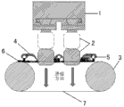
Fig. 2 is existing multifibres incision principle figure;
Fig. 3 is the state diagram that silicon rod is cut to the rounding place when having the multifibres cutting now;
Silicon rod was cut the state diagram behind the circular arc rounding when Fig. 4 was existing multifibres cutting;
Fig. 5 is the structural representation that the present invention reduces the another kind of embodiment of device of solar silicon wafers cutting stria;
Fig. 6 is the structural representation that the present invention reduces the third embodiment of device of solar silicon wafers cutting stria;
Fig. 7 is the structural representation that the present invention reduces the 4th kind of embodiment of device of solar silicon wafers cutting stria;
Fig. 8 is the structural representation that the present invention reduces the 5th kind of embodiment of device of solar silicon wafers cutting stria;
Fig. 9 is the structural representation that the present invention reduces the 6th kind of embodiment of device of solar silicon wafers cutting stria.
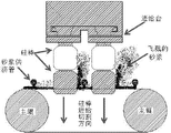
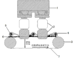
Among the figure, 1. feeding platform, 2. silicon rod, 3. home roll, 4. mortar guiding device, 5. mortar pipe, 6. mortar, 7. cutting steel wire.
The specific embodiment
The present invention is described in detail below in conjunction with the drawings and specific embodiments.
The present invention reduces the method for solar silicon wafers cutting stria, adopt along the direction of routing of cutting steel wire 7, junction, silicon rod 2 both sides at cutting steel wire 7 and silicon rod 2 are provided with mortar guiding device 4, and mortar 6 is effectively fallen back on the gauze, are gathered in the side, end of incoming cables of silicon rod 2.When mortar guiding device 4 adopts rigid material (stainless steel, steel plate, plastics), and the distance between the silicon rod 2 is the 3-5 millimeter; When mortar guiding device 4 adopts soft materials (rubber, synthetic fibers), and the distance between the silicon rod 2 is the 0-2 millimeter; The planform of mortar guiding device 4 is unfixing, and returning the cutting gauze with the mortar water conservancy diversion that can will splash is the Any shape of purpose, reference configuration such as Fig. 1, Fig. 5, Fig. 6, Fig. 7, Fig. 8, shown in Figure 9.The mortar guiding device can be fixed in the arbitrary position that can fix on the gauze, but should note its can not with gauze and ground network warning device interference, the rigging position of most convenient is to be fixed on the mortar pipe 5, or is made as an integral body with mortar pipe 5.
The present invention reduces the structure of the device of solar silicon wafers cutting stria, as shown in Figure 1, comprise two home rolls that be arranged in parallel 3, the excircle of home roll 3 is wound with cutting steel wire 7, be fixed on silicon rod 2 on the feeding platform 1 along direction of routing feeding perpendicular to cutting steel wire 7, when running into cutting steel wire 7, finish cutting, junction at cutting steel wire 7 and silicon rod 2, silicon rod 2 both sides are provided with mortar guiding device 4, mortar guiding device 4 is fixed on the mortar pipe 5 and (or fixedly is assemblied on the cutting chamber inwall, also can design the mortar guiding device wears on the inwall that support is fixed in cutting gauze both sides), mortar pipe 5 is positioned at the top of home roll 3 and cutting steel wire 7, be positioned the cutting bin inwall, be connected with the mortar service.
Design improves principle:
In recent years, many steel wire cuttings of free abrasive particle had all been adopted in the silicon chip section basically, and as shown in Figure 2, multi-thread cutting technique is a novel silicon chip cutting technique that emerges in recent years, and it carries out attrition process by wire drive carborundum abrasive and cuts silicon chip.Compare with traditional interior circle cutting, but the multifibres cutting has that cutting efficiency height, spillage of material are little, cost reduction, silicon chip surface quality height cutting large size material, make things convenient for characteristics such as following process.Cutting technique as a kind of advanced person, multi-thread cutting has replaced the main cutting mode that traditional interior circle is cut into present silicon chip slice processing gradually, at present, Switzerland HCT company, Meyert Burger company, Japan Takatori(high bird), the famous manufacturer of minority such as NTC has successively grasped this key technology, and has released corresponding multifibres cutting off machine product, especially large-sized cutting equipment.
Existing multifibres cutter sweep is in cutting process, mortar cutting power performance when cutting the circular arc chamfering place is not enough, mortar is under the situation of the water conservancy diversion that does not have the silicon chip circular arc chamfering, cutting steel wire band mortar and is rushed at silicon rod with 628m/ minute high speed, have mortar about 60~70% to run into approximately to splash behind the silicon material to scatter, the SIC particle of participating in effectively cutting has reduced many.Through the research classification to the multi-thread cutting stria of solar silicon wafers silicon chip, it is outer unusually to remove broken string, steel wire and mortar etc., and in 6.5 cun, the 8 cun silicon chips, the stria branch of 80% stria silicon chip is at the middle part of silicon chip, and cutting is satisfactory for result in the red frame scope of turnover cutter circular arc.
Above-mentioned defective former appears because: as shown in Figures 3 and 4, be cut to chamfering place mortar and under the water conservancy diversion of chamfering, assemble and turn round and round and major part is brought into to participate in effectively in the silicon rod and cuts.And after cutting the silicon rod circular arc chamfering, mortar is under the situation of the water conservancy diversion that does not have the silicon chip circular arc chamfering, running into splashes behind the silicon material scatters, the water conservancy diversion that has not had the silicon rod circular arc chamfering, mortar is run into silicon rod inlet wire rear flank, splashes and looses, and the effective SiC quantity that participates in cutting significantly reduces, so improve the effectively quantity of cutting sand, be the bad key of middle stria of thoroughly effectively improving the silicon chip cutting technique.
The present invention improves a little and is:
(1) water conservancy diversion material wear-resistant, mortar is splashed to its surface, is difficult for having particle to come off.
(2) mortar guiding device shape is unrestricted, as long as mortar is effectively fallen back on the gauze, is gathered in side, silicon rod end of incoming cables and gets final product.
(3) the mortar guiding device is moderate apart from the silicon rod distance, if mortar guiding device material therefor is really up to the mark, it can not contact silicon rod, and with the anti-scratch silicon rod, it is bad to make the silicon chip generation collapse limit or fragment etc.; If the partly or entirely softer or flexible of mortar guiding device material does not contact with silicon rod and can damage silicon rod, and it is pasted fully mutually with silicon rod, mortar can not splash.
(4) design of mortar guiding device, its major function be, make mortar can be gathered in the side of silicon rod end of incoming cables, rather than splash and nebulize, and it is ideal to form inward turning.
Claims (8)
1. one kind is reduced the method that solar silicon wafers cuts stria, excircle at two home rolls (3) that be arranged in parallel twines cutting steel wire (7), be fixed on the feeding platform (1) silicon rod (2) along perpendicular to the cutting steel wire (7) the direction of routing feeding, it is characterized in that, direction of routing along cutting steel wire (7), junction, silicon rod (2) both sides at cutting steel wire (7) and silicon rod (2) are provided with mortar guiding device (4), mortar (6) is effectively fallen back on the gauze, be gathered in the side, end of incoming cables of silicon rod (2).
2. the method for minimizing solar silicon wafers cutting stria according to claim 1, it is characterized in that, when described mortar guiding device (4) adopts rigid material, and the distance between the silicon rod (2) is the 3-5 millimeter, and described rigid material is selected a kind of in stainless steel, steel plate or the plastics for use.
3. the method for minimizing solar silicon wafers cutting stria according to claim 1, it is characterized in that, when described mortar guiding device (4) adopts soft materials, and the distance between the silicon rod (2) is the 0-2 millimeter, and described soft materials is selected rubber or synthetic fibers for use.
4. the method for minimizing solar silicon wafers cutting stria according to claim 1 is characterized in that described mortar guiding device (4) returns the shape of cutting steel wire (7) for mortar (6) water conservancy diversion that can will splash.
5. one kind is reduced the device that solar silicon wafers cuts stria, it is characterized in that, comprise two home rolls that be arranged in parallel (3), the excircle of home roll (3) is wound with cutting steel wire (7), be fixed on the feeding platform (1) silicon rod (2) along perpendicular to the cutting steel wire (7) the direction of routing feeding, along the direction of routing of cutting steel wire (7), be provided with mortar guiding device (4) in junction, silicon rod (2) both sides of cutting steel wire (7) and silicon rod (2).
6. the device of minimizing solar silicon wafers cutting stria according to claim 5, it is characterized in that, when described mortar guiding device (4) adopts rigid material, and the distance between the silicon rod (2) is the 3-5 millimeter, and described rigid material is selected a kind of in stainless steel, steel plate or the plastics for use.
7. the device of minimizing solar silicon wafers cutting stria according to claim 5, it is characterized in that, when described mortar guiding device (4) adopts soft materials, and the distance between the silicon rod (2) is the 0-2 millimeter, and described soft materials is selected rubber or synthetic fibers for use.
8. according to the device of the described minimizing solar silicon wafers cutting of claim 5 stria, it is characterized in that described mortar guiding device (4) returns the shape of cutting steel wire (7) for mortar (6) water conservancy diversion that can will splash.
Priority Applications (1)
| Application Number | Priority Date | Filing Date | Title |
|---|---|---|---|
| CN2010105643485A CN102107465A (en) | 2010-11-30 | 2010-11-30 | Method and device for reducing cutting line mark of solar silicon slice |
Applications Claiming Priority (1)
| Application Number | Priority Date | Filing Date | Title |
|---|---|---|---|
| CN2010105643485A CN102107465A (en) | 2010-11-30 | 2010-11-30 | Method and device for reducing cutting line mark of solar silicon slice |
Publications (1)
| Publication Number | Publication Date |
|---|---|
| CN102107465A true CN102107465A (en) | 2011-06-29 |
Family
ID=44171802
Family Applications (1)
| Application Number | Title | Priority Date | Filing Date |
|---|---|---|---|
| CN2010105643485A Pending CN102107465A (en) | 2010-11-30 | 2010-11-30 | Method and device for reducing cutting line mark of solar silicon slice |
Country Status (1)
| Country | Link |
|---|---|
| CN (1) | CN102107465A (en) |
Cited By (9)
| Publication number | Priority date | Publication date | Assignee | Title |
|---|---|---|---|---|
| CN102501322A (en) * | 2011-11-03 | 2012-06-20 | 上海申和热磁电子有限公司 | Device and process for high-speed polycrystalline wire cutting |
| CN102601877A (en) * | 2012-04-01 | 2012-07-25 | 苏州协鑫光伏科技有限公司 | Device and method for processing silicon wafer |
| CN103390693A (en) * | 2013-07-29 | 2013-11-13 | 宁晋阳光新能源有限公司 | Method for recycling main roller for solar cell slicing |
| CN103586989A (en) * | 2013-11-25 | 2014-02-19 | 王金生 | Scroll saw cutting machine coated with dissociating abrasives |
| CN107553763A (en) * | 2016-06-30 | 2018-01-09 | 广东先导先进材料股份有限公司 | A kind of method and cutter device of multi-wire saw chip |
| CN108943456A (en) * | 2017-05-23 | 2018-12-07 | 上海新昇半导体科技有限公司 | Mortar intake chute, mortar feeding mechanism and wafer diced system |
| CN111745844A (en) * | 2019-03-26 | 2020-10-09 | 赛维Ldk太阳能高科技(新余)有限公司 | Border seed crystal and preparation method and application thereof |
| CN112871813A (en) * | 2019-11-29 | 2021-06-01 | 隆基绿能科技股份有限公司 | Cleaning method and cleaning device for slicing machine |
| CN114800899A (en) * | 2022-04-19 | 2022-07-29 | 广东高景太阳能科技有限公司 | Monocrystalline silicon wafer color difference improving method and system, storage medium and electronic equipment |
Citations (6)
| Publication number | Priority date | Publication date | Assignee | Title |
|---|---|---|---|---|
| JPH1199462A (en) * | 1997-09-26 | 1999-04-13 | Toshiba Ceramics Co Ltd | Wire saw |
| JP2000000750A (en) * | 1998-06-15 | 2000-01-07 | Toshiba Ceramics Co Ltd | Multiwire saw |
| CN101554757A (en) * | 2009-05-14 | 2009-10-14 | 浙江昱辉阳光能源有限公司 | Cutting method of crystalline silicon blocks |
| CN101791828A (en) * | 2010-02-25 | 2010-08-04 | 晶科能源有限公司 | Deflection angle multi-line cutting method and cutting device thereof |
| CN201587046U (en) * | 2010-02-01 | 2010-09-22 | 晶科能源有限公司 | Silicon chip cutter adopting guide bar |
| WO2010120491A2 (en) * | 2009-04-01 | 2010-10-21 | Cabot Microelectronics Corporation | Self-cleaning wiresaw apparatus and method |
-
2010
- 2010-11-30 CN CN2010105643485A patent/CN102107465A/en active Pending
Patent Citations (6)
| Publication number | Priority date | Publication date | Assignee | Title |
|---|---|---|---|---|
| JPH1199462A (en) * | 1997-09-26 | 1999-04-13 | Toshiba Ceramics Co Ltd | Wire saw |
| JP2000000750A (en) * | 1998-06-15 | 2000-01-07 | Toshiba Ceramics Co Ltd | Multiwire saw |
| WO2010120491A2 (en) * | 2009-04-01 | 2010-10-21 | Cabot Microelectronics Corporation | Self-cleaning wiresaw apparatus and method |
| CN101554757A (en) * | 2009-05-14 | 2009-10-14 | 浙江昱辉阳光能源有限公司 | Cutting method of crystalline silicon blocks |
| CN201587046U (en) * | 2010-02-01 | 2010-09-22 | 晶科能源有限公司 | Silicon chip cutter adopting guide bar |
| CN101791828A (en) * | 2010-02-25 | 2010-08-04 | 晶科能源有限公司 | Deflection angle multi-line cutting method and cutting device thereof |
Cited By (11)
| Publication number | Priority date | Publication date | Assignee | Title |
|---|---|---|---|---|
| CN102501322A (en) * | 2011-11-03 | 2012-06-20 | 上海申和热磁电子有限公司 | Device and process for high-speed polycrystalline wire cutting |
| CN102601877A (en) * | 2012-04-01 | 2012-07-25 | 苏州协鑫光伏科技有限公司 | Device and method for processing silicon wafer |
| CN103390693A (en) * | 2013-07-29 | 2013-11-13 | 宁晋阳光新能源有限公司 | Method for recycling main roller for solar cell slicing |
| CN103390693B (en) * | 2013-07-29 | 2016-04-27 | 宁晋阳光新能源有限公司 | The recycling method of solar cell section home roll |
| CN103586989A (en) * | 2013-11-25 | 2014-02-19 | 王金生 | Scroll saw cutting machine coated with dissociating abrasives |
| CN103586989B (en) * | 2013-11-25 | 2015-12-02 | 王金生 | A kind of saw blade cutting machine applying free abrasive |
| CN107553763A (en) * | 2016-06-30 | 2018-01-09 | 广东先导先进材料股份有限公司 | A kind of method and cutter device of multi-wire saw chip |
| CN108943456A (en) * | 2017-05-23 | 2018-12-07 | 上海新昇半导体科技有限公司 | Mortar intake chute, mortar feeding mechanism and wafer diced system |
| CN111745844A (en) * | 2019-03-26 | 2020-10-09 | 赛维Ldk太阳能高科技(新余)有限公司 | Border seed crystal and preparation method and application thereof |
| CN112871813A (en) * | 2019-11-29 | 2021-06-01 | 隆基绿能科技股份有限公司 | Cleaning method and cleaning device for slicing machine |
| CN114800899A (en) * | 2022-04-19 | 2022-07-29 | 广东高景太阳能科技有限公司 | Monocrystalline silicon wafer color difference improving method and system, storage medium and electronic equipment |
Similar Documents
| Publication | Publication Date | Title |
|---|---|---|
| CN102107465A (en) | Method and device for reducing cutting line mark of solar silicon slice | |
| CN100565935C (en) | Ultra-thin solar silicon slice and cutting technique thereof | |
| CN103407009B (en) | Diamond wire multi-line cutting machine | |
| AU2012247998B2 (en) | Diamond wire saw device | |
| CN101554757A (en) | Cutting method of crystalline silicon blocks | |
| WO2012139498A1 (en) | Three roller multi-wire saw | |
| CN102350741A (en) | Silicon block cutting method | |
| CN201900687U (en) | Improved cutting steel wire | |
| CN203110185U (en) | Cleaning and cutting system for four-guiding-wheel multi-wire cutting machine | |
| CN203792547U (en) | Main roller sand blasting device for multi-wire sawing machine | |
| CN201808158U (en) | Solar silicon chip cutting directing bar | |
| CN206768249U (en) | Prepare the production equipment of Buddha's warrior attendant nickel plating scroll saw | |
| CN202412492U (en) | Cutting device for silicon blocks | |
| CN204278278U (en) | Silicon chip cutting machine tool mortar backplate | |
| CN205112119U (en) | Monocrystalline silicon piece cutting equipment | |
| CN203381055U (en) | Main roll of multi-wire sawing machine | |
| CN203712893U (en) | Slurry baffle for silicon wafer multi-wire sawing machine | |
| CN211566525U (en) | Solar cell crystalline silicon cutting equipment | |
| CN203527671U (en) | Silicon ingot cutting device | |
| CN202147322U (en) | Wire distribution structure of multi-wire cutter for silicon chips | |
| CN201900686U (en) | Special-shaped cutting steel wire with glue coating layer | |
| CN205651410U (en) | Multistation crystal rod material list wire cut electrical discharge machining | |
| CN204955160U (en) | Diamond coping saw of brazing | |
| CN206913481U (en) | A kind of PV800H diamond wire saws machine | |
| CN203579916U (en) | Solar silicon wafer linear cutting groove wheel |
Legal Events
| Date | Code | Title | Description |
|---|---|---|---|
| C06 | Publication | ||
| PB01 | Publication | ||
| C10 | Entry into substantive examination | ||
| SE01 | Entry into force of request for substantive examination | ||
| C12 | Rejection of a patent application after its publication | ||
| RJ01 | Rejection of invention patent application after publication |
Application publication date: 20110629 |