CN101859711B - Method for manufacturing amorphous oxide film - Google Patents
Method for manufacturing amorphous oxide film Download PDFInfo
- Publication number
- CN101859711B CN101859711B CN2010102032047A CN201010203204A CN101859711B CN 101859711 B CN101859711 B CN 101859711B CN 2010102032047 A CN2010102032047 A CN 2010102032047A CN 201010203204 A CN201010203204 A CN 201010203204A CN 101859711 B CN101859711 B CN 101859711B
- Authority
- CN
- China
- Prior art keywords
- film
- hydrogen
- channel layer
- tft
- oxygen
- Prior art date
- Legal status (The legal status is an assumption and is not a legal conclusion. Google has not performed a legal analysis and makes no representation as to the accuracy of the status listed.)
- Expired - Fee Related
Links
- 238000000034 method Methods 0.000 title claims abstract description 68
- 238000004519 manufacturing process Methods 0.000 title abstract description 16
- 229910052739 hydrogen Inorganic materials 0.000 claims abstract description 121
- 239000001257 hydrogen Substances 0.000 claims abstract description 121
- UFHFLCQGNIYNRP-UHFFFAOYSA-N Hydrogen Chemical compound [H][H] UFHFLCQGNIYNRP-UHFFFAOYSA-N 0.000 claims abstract description 93
- QVGXLLKOCUKJST-UHFFFAOYSA-N atomic oxygen Chemical compound [O] QVGXLLKOCUKJST-UHFFFAOYSA-N 0.000 claims abstract description 57
- 239000001301 oxygen Substances 0.000 claims abstract description 57
- 229910052760 oxygen Inorganic materials 0.000 claims abstract description 57
- 239000000758 substrate Substances 0.000 claims abstract description 39
- 230000005669 field effect Effects 0.000 claims abstract description 35
- 229910052738 indium Inorganic materials 0.000 claims abstract description 4
- 229910052725 zinc Inorganic materials 0.000 claims abstract description 4
- 238000004544 sputter deposition Methods 0.000 abstract description 7
- 230000001939 inductive effect Effects 0.000 abstract 1
- 239000010408 film Substances 0.000 description 182
- 239000007789 gas Substances 0.000 description 42
- 239000000463 material Substances 0.000 description 32
- XKRFYHLGVUSROY-UHFFFAOYSA-N Argon Chemical compound [Ar] XKRFYHLGVUSROY-UHFFFAOYSA-N 0.000 description 26
- 150000002431 hydrogen Chemical class 0.000 description 26
- 239000010409 thin film Substances 0.000 description 25
- 230000015572 biosynthetic process Effects 0.000 description 20
- 150000002500 ions Chemical class 0.000 description 18
- 230000000052 comparative effect Effects 0.000 description 14
- 229910052805 deuterium Inorganic materials 0.000 description 14
- YZCKVEUIGOORGS-OUBTZVSYSA-N Deuterium Chemical compound [2H] YZCKVEUIGOORGS-OUBTZVSYSA-N 0.000 description 13
- 229910052786 argon Inorganic materials 0.000 description 13
- 239000004065 semiconductor Substances 0.000 description 13
- 229910007541 Zn O Inorganic materials 0.000 description 10
- 229910052751 metal Inorganic materials 0.000 description 10
- 239000003595 mist Substances 0.000 description 10
- 238000013459 approach Methods 0.000 description 9
- 239000011521 glass Substances 0.000 description 9
- 239000000523 sample Substances 0.000 description 9
- 125000004435 hydrogen atom Chemical group [H]* 0.000 description 8
- 239000002184 metal Substances 0.000 description 7
- 238000001259 photo etching Methods 0.000 description 7
- 238000004458 analytical method Methods 0.000 description 6
- 238000011156 evaluation Methods 0.000 description 6
- 238000002347 injection Methods 0.000 description 6
- 239000007924 injection Substances 0.000 description 6
- 238000004549 pulsed laser deposition Methods 0.000 description 6
- 238000001004 secondary ion mass spectrometry Methods 0.000 description 6
- 238000002441 X-ray diffraction Methods 0.000 description 5
- 239000002800 charge carrier Substances 0.000 description 5
- 238000005259 measurement Methods 0.000 description 5
- 230000003647 oxidation Effects 0.000 description 5
- 238000007254 oxidation reaction Methods 0.000 description 5
- 238000000059 patterning Methods 0.000 description 5
- 239000004033 plastic Substances 0.000 description 5
- 229920003023 plastic Polymers 0.000 description 5
- 229920006255 plastic film Polymers 0.000 description 5
- 239000002985 plastic film Substances 0.000 description 5
- 229910052782 aluminium Inorganic materials 0.000 description 4
- 150000001875 compounds Chemical class 0.000 description 4
- 239000007772 electrode material Substances 0.000 description 4
- GPRLSGONYQIRFK-UHFFFAOYSA-N hydron Chemical compound [H+] GPRLSGONYQIRFK-UHFFFAOYSA-N 0.000 description 4
- 238000012546 transfer Methods 0.000 description 4
- RPAJSBKBKSSMLJ-DFWYDOINSA-N (2s)-2-aminopentanedioic acid;hydrochloride Chemical compound Cl.OC(=O)[C@@H](N)CCC(O)=O RPAJSBKBKSSMLJ-DFWYDOINSA-N 0.000 description 3
- 229920002799 BoPET Polymers 0.000 description 3
- 229910006404 SnO 2 Inorganic materials 0.000 description 3
- 239000013078 crystal Substances 0.000 description 3
- 238000002425 crystallisation Methods 0.000 description 3
- 230000008025 crystallization Effects 0.000 description 3
- 238000009826 distribution Methods 0.000 description 3
- 229910052733 gallium Inorganic materials 0.000 description 3
- 229910052732 germanium Inorganic materials 0.000 description 3
- 238000009413 insulation Methods 0.000 description 3
- 239000004973 liquid crystal related substance Substances 0.000 description 3
- SLIUAWYAILUBJU-UHFFFAOYSA-N pentacene Chemical compound C1=CC=CC2=CC3=CC4=CC5=CC=CC=C5C=C4C=C3C=C21 SLIUAWYAILUBJU-UHFFFAOYSA-N 0.000 description 3
- 229910052710 silicon Inorganic materials 0.000 description 3
- 125000003118 aryl group Chemical group 0.000 description 2
- 229910052796 boron Inorganic materials 0.000 description 2
- 238000005266 casting Methods 0.000 description 2
- 239000011248 coating agent Substances 0.000 description 2
- 238000000576 coating method Methods 0.000 description 2
- 239000000470 constituent Substances 0.000 description 2
- 229910021419 crystalline silicon Inorganic materials 0.000 description 2
- 238000000151 deposition Methods 0.000 description 2
- 230000008021 deposition Effects 0.000 description 2
- -1 deuterium ion Chemical class 0.000 description 2
- 230000000694 effects Effects 0.000 description 2
- 238000000313 electron-beam-induced deposition Methods 0.000 description 2
- 238000005516 engineering process Methods 0.000 description 2
- 230000008020 evaporation Effects 0.000 description 2
- 238000001704 evaporation Methods 0.000 description 2
- 238000010438 heat treatment Methods 0.000 description 2
- 239000011810 insulating material Substances 0.000 description 2
- 230000002093 peripheral effect Effects 0.000 description 2
- 229920005644 polyethylene terephthalate glycol copolymer Polymers 0.000 description 2
- 230000005855 radiation Effects 0.000 description 2
- 229920006395 saturated elastomer Polymers 0.000 description 2
- 238000004611 spectroscopical analysis Methods 0.000 description 2
- 229910052718 tin Inorganic materials 0.000 description 2
- 229910052727 yttrium Inorganic materials 0.000 description 2
- 229910052726 zirconium Inorganic materials 0.000 description 2
- 239000004215 Carbon black (E152) Substances 0.000 description 1
- 229930194542 Keto Natural products 0.000 description 1
- 229910020923 Sn-O Inorganic materials 0.000 description 1
- 229910018956 Sn—In Inorganic materials 0.000 description 1
- 229910017875 a-SiN Inorganic materials 0.000 description 1
- 238000000862 absorption spectrum Methods 0.000 description 1
- 229910021417 amorphous silicon Inorganic materials 0.000 description 1
- 238000005452 bending Methods 0.000 description 1
- 230000005540 biological transmission Effects 0.000 description 1
- 230000000711 cancerogenic effect Effects 0.000 description 1
- 231100000315 carcinogenic Toxicity 0.000 description 1
- 239000004020 conductor Substances 0.000 description 1
- 230000005516 deep trap Effects 0.000 description 1
- 230000006735 deficit Effects 0.000 description 1
- 230000001419 dependent effect Effects 0.000 description 1
- 230000000881 depressing effect Effects 0.000 description 1
- 238000010790 dilution Methods 0.000 description 1
- 239000012895 dilution Substances 0.000 description 1
- 239000006185 dispersion Substances 0.000 description 1
- 238000001312 dry etching Methods 0.000 description 1
- 238000013213 extrapolation Methods 0.000 description 1
- 239000004744 fabric Substances 0.000 description 1
- 229910052737 gold Inorganic materials 0.000 description 1
- 229930195733 hydrocarbon Natural products 0.000 description 1
- 150000002430 hydrocarbons Chemical class 0.000 description 1
- 238000005468 ion implantation Methods 0.000 description 1
- 125000000468 ketone group Chemical group 0.000 description 1
- 238000010030 laminating Methods 0.000 description 1
- 238000011031 large-scale manufacturing process Methods 0.000 description 1
- 239000012528 membrane Substances 0.000 description 1
- 238000002156 mixing Methods 0.000 description 1
- 229910052759 nickel Inorganic materials 0.000 description 1
- 230000003287 optical effect Effects 0.000 description 1
- 238000005268 plasma chemical vapour deposition Methods 0.000 description 1
- 238000009832 plasma treatment Methods 0.000 description 1
- 229910052697 platinum Inorganic materials 0.000 description 1
- 229910021420 polycrystalline silicon Inorganic materials 0.000 description 1
- 229920000642 polymer Polymers 0.000 description 1
- 229920006254 polymer film Polymers 0.000 description 1
- 229920005591 polysilicon Polymers 0.000 description 1
- 238000012545 processing Methods 0.000 description 1
- 239000010453 quartz Substances 0.000 description 1
- 238000011160 research Methods 0.000 description 1
- 238000012827 research and development Methods 0.000 description 1
- VYPSYNLAJGMNEJ-UHFFFAOYSA-N silicon dioxide Inorganic materials O=[Si]=O VYPSYNLAJGMNEJ-UHFFFAOYSA-N 0.000 description 1
- 238000005245 sintering Methods 0.000 description 1
- 231100000419 toxicity Toxicity 0.000 description 1
- 230000001988 toxicity Effects 0.000 description 1
- 239000012780 transparent material Substances 0.000 description 1
Images


Classifications
-
- H—ELECTRICITY
- H01—ELECTRIC ELEMENTS
- H01L—SEMICONDUCTOR DEVICES NOT COVERED BY CLASS H10
- H01L29/00—Semiconductor devices adapted for rectifying, amplifying, oscillating or switching, or capacitors or resistors with at least one potential-jump barrier or surface barrier, e.g. PN junction depletion layer or carrier concentration layer; Details of semiconductor bodies or of electrodes thereof ; Multistep manufacturing processes therefor
- H01L29/66—Types of semiconductor device ; Multistep manufacturing processes therefor
- H01L29/68—Types of semiconductor device ; Multistep manufacturing processes therefor controllable by only the electric current supplied, or only the electric potential applied, to an electrode which does not carry the current to be rectified, amplified or switched
- H01L29/76—Unipolar devices, e.g. field effect transistors
- H01L29/772—Field effect transistors
- H01L29/78—Field effect transistors with field effect produced by an insulated gate
- H01L29/786—Thin film transistors, i.e. transistors with a channel being at least partly a thin film
- H01L29/7869—Thin film transistors, i.e. transistors with a channel being at least partly a thin film having a semiconductor body comprising an oxide semiconductor material, e.g. zinc oxide, copper aluminium oxide, cadmium stannate
- H01L29/78693—Thin film transistors, i.e. transistors with a channel being at least partly a thin film having a semiconductor body comprising an oxide semiconductor material, e.g. zinc oxide, copper aluminium oxide, cadmium stannate the semiconducting oxide being amorphous
-
- H—ELECTRICITY
- H01—ELECTRIC ELEMENTS
- H01L—SEMICONDUCTOR DEVICES NOT COVERED BY CLASS H10
- H01L29/00—Semiconductor devices adapted for rectifying, amplifying, oscillating or switching, or capacitors or resistors with at least one potential-jump barrier or surface barrier, e.g. PN junction depletion layer or carrier concentration layer; Details of semiconductor bodies or of electrodes thereof ; Multistep manufacturing processes therefor
- H01L29/02—Semiconductor bodies ; Multistep manufacturing processes therefor
- H01L29/06—Semiconductor bodies ; Multistep manufacturing processes therefor characterised by their shape; characterised by the shapes, relative sizes, or dispositions of the semiconductor regions ; characterised by the concentration or distribution of impurities within semiconductor regions
-
- H—ELECTRICITY
- H01—ELECTRIC ELEMENTS
- H01L—SEMICONDUCTOR DEVICES NOT COVERED BY CLASS H10
- H01L29/00—Semiconductor devices adapted for rectifying, amplifying, oscillating or switching, or capacitors or resistors with at least one potential-jump barrier or surface barrier, e.g. PN junction depletion layer or carrier concentration layer; Details of semiconductor bodies or of electrodes thereof ; Multistep manufacturing processes therefor
- H01L29/66—Types of semiconductor device ; Multistep manufacturing processes therefor
- H01L29/66007—Multistep manufacturing processes
- H01L29/66075—Multistep manufacturing processes of devices having semiconductor bodies comprising group 14 or group 13/15 materials
- H01L29/66227—Multistep manufacturing processes of devices having semiconductor bodies comprising group 14 or group 13/15 materials the devices being controllable only by the electric current supplied or the electric potential applied, to an electrode which does not carry the current to be rectified, amplified or switched, e.g. three-terminal devices
- H01L29/66409—Unipolar field-effect transistors
- H01L29/66477—Unipolar field-effect transistors with an insulated gate, i.e. MISFET
- H01L29/66742—Thin film unipolar transistors
-
- H—ELECTRICITY
- H01—ELECTRIC ELEMENTS
- H01L—SEMICONDUCTOR DEVICES NOT COVERED BY CLASS H10
- H01L29/00—Semiconductor devices adapted for rectifying, amplifying, oscillating or switching, or capacitors or resistors with at least one potential-jump barrier or surface barrier, e.g. PN junction depletion layer or carrier concentration layer; Details of semiconductor bodies or of electrodes thereof ; Multistep manufacturing processes therefor
- H01L29/66—Types of semiconductor device ; Multistep manufacturing processes therefor
- H01L29/66007—Multistep manufacturing processes
- H01L29/66969—Multistep manufacturing processes of devices having semiconductor bodies not comprising group 14 or group 13/15 materials
Landscapes
- Engineering & Computer Science (AREA)
- Microelectronics & Electronic Packaging (AREA)
- Power Engineering (AREA)
- Physics & Mathematics (AREA)
- Ceramic Engineering (AREA)
- Condensed Matter Physics & Semiconductors (AREA)
- General Physics & Mathematics (AREA)
- Computer Hardware Design (AREA)
- Manufacturing & Machinery (AREA)
- Thin Film Transistor (AREA)
- Dram (AREA)
Abstract
The invention relates to a method for manufacturing an amorphous oxide film which contains In or Zn and is used as a channel layer of a field effect transistor. The method comprises the steps of: placing a substrate in a film forming device and forming the amorphous oxide film by sputtering on the substrate while inducing oxygen and hydrogen in the film forming device with a respective partial pressure, wherein the partial pressure of hydrogen is 0.001 to 0.01 Pa and the partial pressure of the oxygen is 0.008 to 0.5Pa.
Description
The application is that application number is 200680032534.6, the applying date is on September 5th, 2006, denomination of invention is divided an application for the application for a patent for invention of " use amorphous oxide film as the field-effect transistor of channel layer, use amorphous oxide film as the manufacturing approach of the field-effect transistor of channel layer and the manufacturing approach of amorphous oxide film ".
Technical field
The field-effect transistor that the present invention relates to have the channel layer that forms by amorphous oxides and have the transistor characteristic that is applicable to display device etc.
Background technology
Field-effect transistor (being sometimes referred to as " FET " hereinafter) has gate electrode, source electrode and drain electrode.In addition, field-effect transistor is an active device, wherein, is controlled at the electric current that flows in the channel layer, the electric current that promptly between source electrode and drain electrode, flows through being applied to voltage gate electrode.Particularly, use the film that on the dielectric base of pottery, glass or plastics, forms to be called as thin-film transistor (being sometimes referred to as " TFT " hereinafter) as the FET of channel layer.
Through using film forming technology, can be TFT useful and easily be formed in the relatively large substrate, the result, TFT has been widely used as the driving element and the switching device of the flat-panel monitor such as LCD.That is to say that in AMLCD (ALCD), the TFT of the correspondence that use forms carries out the conducting of each image pixel/shutoff operation on substrate of glass.In addition, in high-performance organic LED display (OLED), effective control of pixel current is carried out in expectation by TFT.In addition, realize having the liquid crystal display device of superior performance, wherein, formed the drive circuit of forming by TFT in the substrate in the outer peripheral areas of image-region.
Recently the most widely used TFT uses polysilicon film or amorphous silicon film as channel layer materials.Above-mentioned TFT is called as metal-insulator-semiconductor field effect transistor (MIS-FET).For pixel driver, use non-crystalline silicon tft, and for the peripheral circuit of driver and controller, reality has been used high performance multi-crystal TFT.
Yet in the TFT that comprises non-crystalline silicon tft and multi-crystal TFT that has developed up to now, device formation needs high-temperature process, thereby is difficult in the substrate such as plastic plate or plastic film, form TFT.
On the other hand, in recent years, through being formed on TFT on polymer sheet or the polymer film exploitation that comes to realize energetically flexible display as the drive circuit of LCD or OLED.As the material that can on plastic film etc., form, the organic semiconductor film that can form has at low temperatures caused people's attention.
For example, as a kind of organic semiconductor film, the research and development of pentacene etc. are implemented.Above-mentioned organic semiconductor all has aromatic rings, and when making their crystallizations, can on the laminating direction of aromatic rings, obtain high carrier mobility.For example, reported when being used for active layer to pentacene that carrier mobility is approximately 0.5cm (Vs)
-1And approximate the carrier mobility of amorphous Si-MOSFET greatly.
Yet the organic semiconductor such as pentacene has poor thermal stability (<150 ℃) and toxicity (carcinogenic nature) unfriendly, and does not therefore realize actual device now.
In addition, in recent years, as a kind of material that can be applied to the channel layer of TFT, oxide material has begun to cause people's attention.
For example, carried out using mainly of the exploitation of the polycrystalline sull of the transparent and electrically conductive that constitutes by ZnO energetically as the TFT of channel layer.Above-mentioned film can form and thereby can be formed in the substrate such as plastic plate or plastic film with relatively low temperature.Yet, because the compound that mainly is made up of ZnO at room temperature can not form stable amorphous phase, but form the polycrystalline phase, so can not increase owing to the scattering on polycrystalline grain interface causes electron mobility.In addition, because change the shape of polycrystalline grain and connection therebetween significantly, so the characteristic of TFT is disperseed through film build method.
Recently, reported a kind of thin-film transistor, wherein, used amorphous oxides based on In-Ga-Zn-O (people such as K.Nomura, Nature Vol.432, p.488-492, Nov.2004).This transistor can at room temperature be formed on plastics or the substrate of glass.In addition, with about field-effect mobility of 6 to 9, can obtain the transistor characteristic of nomal closed type.In addition, advantageously, this transistor is transparent for visible light.
When inventor of the present invention studies the thin-film transistor that has used based on the amorphous oxides of In-Ga-Zn-O, although the component of depending on and working condition have also produced the hysteresis phenomenon of the transistor characteristic (Id-Vg characteristic) of TFT sometimes.
When being used for above-mentioned TFT the image element circuit of display device for example, being created in of aforesaid hysteresis phenomenon causes change in the operation of wanting driven organic LED, liquid crystal etc., and the result has reduced the picture quality of display device.
Summary of the invention
According to the present invention, reduce above-mentioned hysteresis phenomenon through suitably designing the oxide material that will be used for transistor channel.
In addition, when being used for the channel layer of TFT to amorphous oxide material, electronic carrier concentration is set in the desired range (such as about 10
14To 10
18/ cm
3Scope in).In addition, in order to ensure the reproducibility of transistor characteristic and homogeneity this two, the control device that is used for accurately controlling electronic carrier concentration is provided.
In addition, through suitably being designed for the method that formation will be used for the oxide material of transistor channel, the present invention also provides a kind of method that is used to form the film with electronic carrier concentration desired and that have excellent control.
Field-effect transistor according to one aspect of the invention includes the channel layer that comprises amorphous oxide film, and this amorphous oxide film comprises hydrogen or deuterium.
At first, the hydrogen or the concentration of deuterium that are included in the amorphous oxide film are set at 10
16To 10
20/ cm
3Scope in or be set at 10
17To 10
19/ cm
3Scope in.
In addition, represent to comprise the component of the amorphous oxide film of hydrogen or deuterium with the following equality that does not comprise hydrogen: [(Sn
1-xM4
x) O
2]
a[(In
1-yM3
y)
2O
3] b [Zn
1-zM2
zO]] c, wherein, 0≤x≤1,0≤y≤1,0≤z≤1; 0≤a<1,0≤b<1,0≤c<1, and satisfy a+b+c=1; M4 is an element (Si, Ge, perhaps Zr) that has in the IV family of the atomic number littler than Sn, and M3 is an element (B in Lu or the III-th family with atomic number littler than In; Al, Ga, perhaps Y), and M2 is an element (Mg or Ca) that has in the II family of the atomic number littler than Zn.Especially, M3 comprises Ga.
In addition, according to another aspect of the present invention, provide a kind of method that is used to make amorphous oxide film, this amorphous oxide film said method comprising the steps of: in film-forming apparatus, place substrate as the channel layer of field-effect transistor; And be pressed in predetermined separately branch introduce oxygen and comprise the gas (except that steam) of hydrogen atom in the film-forming apparatus in, in this substrate, form amorphous oxide film.
Especially, carry out film build method, and the partial pressure of oxygen between film forming stage is set to 0.01Pa or higher through sputtering method.
In addition, according to another aspect of the present invention, provide a kind of manufacturing equipment that is used to make amorphous oxide film, said amorphous oxide film is formed in the substrate and is used as the channel layer of field-effect transistor, and said equipment comprises: film forming room; Vacuum extractor is used for film forming room inside is vacuumized; The substrate holding device is used for remaining on film forming room to substrate; Material source is placed as towards the substrate holding device; Energy source is used to make the material evaporation of material source; Be used for providing the device of hydrogen in film forming room; And the device that is used for providing oxygen in film forming room.
With reference to accompanying drawing, from the description of following illustrative embodiment, other characteristics of the present invention will become obvious.
Description of drawings
Figure 1A is according to the cross section view with thin-film transistor of top gate structure of the present invention.
Figure 1B is according to the cutaway view with thin-film transistor of bottom grating structure of the present invention.
Fig. 2 A shows the curve chart according to the transistor characteristic of thin-film transistor of the present invention.
Fig. 2 B shows the curve chart according to the transfer characteristic of thin-film transistor of the present invention.
Fig. 3 A shows the curve chart according to the lagging characteristics of the thin-film transistor of comparative example.
Fig. 3 B shows the curve chart according to the lagging characteristics of the thin-film transistor of an example of the present invention.
Fig. 4 shows the curve chart based on the electronic carrier concentration and the relation between the oxygen partial pressure between film forming stage of the amorphous oxide film of In-Ga-Zn-O.
Fig. 5 is the sketch map of the manufacturing equipment of amorphous oxides film.
Fig. 6 shows the curve chart of the relation between the amount of the hydrogen that mixes in resistivity and the amorphous oxide film based on In-Ga-Zn-O.
Fig. 7 shows the curve chart of the distribution of hydrogen concentration on the depth direction of measuring through SIMS.
Embodiment
Hereinafter, will be described in detail embodiments of the invention with reference to accompanying drawing.
Figure 1A and 1B be illustrate separately according to thin-film transistor of the present invention, be the cross section view of an embodiment of TFT.Figure 1A shows the cross section view of top gate structure, wherein, on semiconductor channel layer 11, forms gate insulating film 12 and gate electrode 15 with the sort of order.Figure 1B shows the cutaway view of bottom grating structure, wherein, on gate electrode 15, forms gate insulating film 12 and semiconductor channel layer 11 with the sort of order.Position relation according to interface between channel layer and the dielectric film and electrode calls cross structure to the structure shown in Figure 1A, and calls reverse interleaved structure to the structure shown in Figure 1B.
Shown in Figure 1A, on the semiconductor channel layer 11 that is formed in the substrate 10, sequentially form source electrode 13, drain electrode 14, gate insulating film 12, gate electrode 15, so that form field-effect transistor with top gate structure (cross structure).In addition, shown in Figure 1B, on the gate electrode 15 that is formed in the substrate 10, sequentially form gate insulating film 12, semiconductor channel layer 11, source electrode 13 and drain electrode 14, so that form field-effect transistor with bottom grating structure (reverse interleaved structure).
Each has three terminal devices of gate electrode 15, source electrode 13 and drain electrode 14 naturally at the field-effect transistor shown in Figure 1A and Figure 1B.Above-mentioned field-effect transistor is the active device with following function, wherein, comes the electric current I d of control flows through channel layer through apply voltage Vg to gate electrode, the electric current I d that promptly between source electrode and drain electrode, flows.
In the present invention, the TFT structure is not limited to said structure, and also can use any top grid or bottom grating structure, promptly any staggered or reverse interleaved structure.
Fig. 2 A and 2B show the typical characteristics of field-effect transistor of the present invention (TFT).From have the structure that will example 1, describe, and the field-effect transistor that forms through the manufacturing approach of wherein describing in obtain the characteristic of TFT.When between source electrode and drain electrode, applying the voltage Vd of about 5V, and when gate voltage Vg in 0 conducting and when turn-offing between 5V, can (between conducting and turn-offing) be controlled at the electric current I d that flows between source electrode and the drain electrode.Fig. 2 A shows the Id-Vd characteristic under the different Vg values, and Fig. 2 B shows the Id-Vg characteristic (transfer characteristic) under the voltage Vd of 6V.
The channel layer of the TFT of this embodiment is formed by the amorphous oxide film that comprises hydrogen or deuterium.
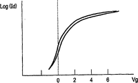
With reference to figure 3A and 3B, with describing through adding the effect that hydrogen obtains, the minimizing of hysteresis phenomenon just to channel layer.Fig. 3 A and 3B show the TFT transistor characteristic that in comparative example 1 and example 1, obtains respectively.That is to say, in example 1, add hydrogen, and in comparative example 1, do not add hydrogen to channel layer to channel layer.
Hysteresis phenomenon means, for example, in order to assess the TFT transfer characteristic, during (upwards with downwards) scanning Vg, through upwards scanning shown in Fig. 3 A and scanning downwards, the value of Id is different in fixing Vd.When under predetermined Vg, the Id value is when upwards altering a great deal between scanning and the downward scanning, and hysteresis phenomenon is very big; Thereby in order accurately to control Id, the device with little hysteresis phenomenon is preferred.
When not comprising hydrogen, the hysteresis phenomenon characteristic and when having used according to the channel layer that comprises hydrogen of the present invention, can obtain the device with little hysteresis phenomenon shown in Fig. 3 B shown in Fig. 3 A.
From the viewpoint of physics, can't be expressly understood the reason that hysteresis phenomenon reduces when applying the oxide that comprises hydrogen to channel layer.A kind of reason of estimation is unordered through adding the partial structurtes that hydrogen alleviates in the noncrystal membrane, and the result is to have realized that charge carrier is not easy captive non crystalline structure (quantity of deep trap reduces).In addition, can also be interpreted as through adding hydrogen and reduce the structural disorder on the interface between channel layer and the dielectric film, and the result is to have realized that between channel layer and dielectric film charge carrier is not easy captive interface to channel layer.
In order to assess hysteresis phenomenon, through when being fixed on source-drain voltage Vd on 5 the appropriate values between 30V, (up or down) raster voltage Vg measures Id (source-drain current) in-10 to 30v scope.In this measures, transistor characteristic is in voltage in the saturation region as Vd, and between conducting and off state, scans Vg.Yet, because can depend on transistor characteristic and transistor arrangement is confirmed the value of Vg and Vd, so always be not restricted to Vg and Vd in the above-mentioned scope.
Can assess the size of hysteresis phenomenon through the difference between Id-Vg curve that upwards scans and the Id-Vg curve that scans downwards.The area of the ring that for example, can obtain Id-Vg curve and the downward Id-Vg curve that scans from upwards scanning is used for this assessment.When this area is very little, we can say that hysteresis phenomenon is very little.In addition, can use difference DELTA Vt=|Vtu-Vtd| to assess the size of hysteresis phenomenon, wherein, Vtu is the threshold voltage of from the Id-Vg curve of upwards scanning, estimating, and Vtd is the threshold voltage of from the Id-Vg curve of downward scanning, estimating.Hereinafter, this Δ Vt is called as threshold shift.Little Δ Vt representes little hysteresis phenomenon.
Be used for the thin-film transistor of its channel layer by means of the oxide that comprises hydrogen according to use of the present invention, can realize having the thin-film transistor of little Δ Vt.
Because the threshold shift of thin-film transistor of the present invention depend on device architecture, channel material, evaluation condition, or the like, therefore for example under predetermined condition, preferably be made as steady state value to the voltage that is applied on the device.An assessment example as thin-film transistor of the present invention; Can use threshold shift to carry out assessment; This threshold shift is under the constant Vg of 10V, obtains in the situation with sweep speed (upwards with downwards) scanning Vg in-5 to 15V scope of 100mV/ second.Particularly, under above-mentioned evaluation condition, threshold shift can be reduced to 2V or lower, is preferably 1V or lower, and more preferably is 0.5V or lower.
The degree of required hysteresis phenomenon depends on the application of thin-film transistor, the circuit structure that will use or the like.For example, use, require relatively low for liquid crystal display and electrophoretic display; Yet,, need higher degree (littler hysteresis phenomenon) for organic EL display device, arithmetical circuit or the like.For example, use for organic EL display device, threshold shift is preferably 2V or lower, more preferably is 1V or lower.In addition, for more high performance organic EL display device, threshold shift is preferably 0.5V or lower.
(hydrogen concentration and electronic carrier concentration)
In addition, studied thin-film transistor with the channel layer that constitutes by amorphous oxides.In order to obtain excellent TFT characteristic, advantageously, use to have 0.0001 the semi-insulating amorphous oxide film of conductivity in the 0.1S/cm scope as channel layer.In order to obtain aforesaid conductivity, although depend on the material component of channel layer, preferably formation has about 10
14To 10
18/ cm
3The amorphous oxide film of electronic carrier concentration.
When conductivity during greater than 0.1S/cm, just becoming is difficult to form the transistor of normal off, and is difficult to form the transistor with big conducting/shutoff ratio.Under opposite extreme situations, even when having applied gate voltage, can not the Controlling Source electrode and drain electrode between flow of current with stop, and thereby can not obtain transistor operation (switch).
On the other hand, when having used insulating material, that is to say that during less than 0.0001S/cm, just becoming is difficult to increase the conducting electric current in conductivity.Under opposite extreme situations, even when having applied gate voltage, can not the Controlling Source electrode and drain electrode between flow of current with stop, and thereby can not obtain the transistor operation.
For the conductivity and the electronic carrier concentration of controlled oxidation thing, between film forming stage, controlled partial pressure of oxygen.That is to say, through the control partial pressure of oxygen, the oxygen deficit in the major control film, thereby control electronic carrier concentration.Fig. 4 shows the carrier concentration that when the sull that forms with sputtering method based on In-Ga-Zn-O, the obtains curve chart to a dependent example of partial pressure of oxygen.In fact with the High Accuracy Control partial pressure of oxygen time, obtained to have 10
14To 10
18/ cm
3The semi-insulating amorphous oxide film of carrier concentration, and when being applied to channel layer to a film that obtains like this, can form good TFT.As shown in Figure 4, when typically when approximately the partial pressure of oxygen of 0.005Pa is carried out film forming, can obtain semi-insulating film.When dividing potential drop during greater than 0.01Pa, form dielectric film, and on the other hand, when dividing potential drop during, form film with too high conductivity less than 0.001Pa; Thereby, preferably be not applied to channel layer to the film of such formation.Yet as shown in Figure 4, because carrier concentration changes with the variation in the partial pressure of oxygen very delicately, so characteristic receives the appreciable impact of minor variations in the membrance casting condition, the result is tending towards being difficult to obtain the reproducibility of TFT characteristic.
According to the present invention, control electronic carrier concentration through adding hydrogen (or deuterium).Through the deep research that inventor of the present invention carried out, having found can be through adding the amount that hydrogen is controlled electronic carrier to amorphous oxide film.
For example, in order to realize about 10
18/ cm
3Electronic carrier concentration, although depend on partial pressure of oxygen and the material component between film forming stage, also can add hydrogen so that have about 10
18To 10
20/ cm
3Concentration.In this case, can carry out control through the amount of control hydrogen doping thing to electronic carrier concentration.In addition, can also control electronic carrier concentration through the amount of hydrogen doping thing and the amount of anoxic.
Therefore, in order to form the TFT with excellent characteristic, the concentration of the hydrogen of interpolation preferably is controlled in 10
16To 10
20/ cm
3Scope in.Although the partial pressure of oxygen of depending on and material component through the interpolation of above-mentioned hydrogen, can realize having about 10
14To 10
18/ cm
3Electronic carrier concentration and be suitable for sull as the channel layer of TFT.
Particularly, when being made as 10 to hydrogen concentration
19/ cm
3Or more hour, can realize transistorized normal off operation and big conducting/shutoff ratio.In addition, hydrogen concentration preferably is set as 10
17/ cm
3Or higher, and through 10
17/ cm
3Or higher hydrogen concentration, can more effectively reduce transistorized hysteresis phenomenon.
For example, can assess hydrogen concentration through secondary ion mass spectrometry (SIMS).Although depend on assessment apparatus, detectable limit is approximately 10
17/ cm
3In zone less than detectable limit, can be through with the hydrogen concentration in the film be used to add between the technological parameter (hydrogen dividing potential drop or after a while with the ion injection rate between the film forming stage of describing) of hydrogen and exist the extrapolation that is assumed to the basis of linear relationship to come to obtain indirectly hydrogen concentration.
The constituent of the channel layer of representing with following equality (not comprising hydrogen) to constitute by the amorphous oxides that has comprised hydrogen among the present invention:
[(Sn
1-xM4
x)O
2]a·[(In
1-yM3
y)
2O
3]b·[(Zn
1-zM2
zO)]c
Wherein, satisfy 0≤x≤1,0≤y≤1,0≤z≤1,0≤a<1,0≤b<1,0≤c<1, and a+b+c=1,
M4 is the element (Si, Ge or Zr) with IV family of the atomic number littler than Sn,
M3 is Lu or the element (B, Al, Ga or Y) with III-th family of the atomic number littler than In, and
M2 is the element (Mg or Ca) with II family of the atomic number littler than Zn.
In above-mentioned constituent, particularly, combination is preferred, that is, and and [(In
1-yGa
y)
2O
3] b [(ZnO)] c, wherein, satisfy 0≤y≤1,0<b<1, and 0<c<1, and [(SnO
2)] a [(In
2O
3)] b [(ZnO)] c, wherein, satisfy 0≤a≤1,0<b<1, and 0<c<1.
For example, can realize according to the amorphous oxide film that comprises hydrogen of the present invention with following component.That is to say that amorphous oxide film has to be positioned at and has 3 peak Ga
2O
3, In
2O
3, and the triangle of ZnO in two heavy ends or three heavy ends, perhaps have to be positioned at and have 3 peak SnO
2, In
2O
3, and the triangle of ZnO in two heavy ends or three heavy ends.In some cases, can make some interior three heavy ends crystallization of specific components scope.Especially, heavy ends are also not preferred, and this is because it is by crystallization.For example, two kinds two heavy ends in having comprised above-mentioned 3 kinds of compounds (being arranged in the component on above-mentioned triangle one side), the component based on In-Zn-O that includes the In of 20 to 70 atomic percents can form amorphous film.In addition, for component, can form amorphous film by the component of the In that comprises 20 to 80 atomic percents based on Sn-In-O.
When as described in the invention, adding in the amorphous oxide film, can at room temperature further stablize this amorphous film to hydrogen atom.Therefore, can in very wide triple compositional range, form amorphous oxides.
(manufacturing approach)
Be used to form according to the method that comprises the specific amorphous oxides of hydrogen of the present invention as a kind of, for example, can mention:
(1) is used for depressing the method that when film-forming apparatus provides the gas (except that steam) that comprises hydrogen atom, forms film at predetermined branch between film forming stage;
(2) be used to use the material source that comprises hydrogen to form the method for film; And
(3) be used to form film, inject through ion then or hydrogen plasma process and to its inner method of adding hydrogen.
In superincumbent those methods, consider the controllability of hydrogen concentration, the method (3) of using ion to inject is preferred.Yet, because injecting after film forming, carries out in ion, thus increased the number of step unfriendly, and on film thickness direction, also produced the distribution of hydrogen concentration unfriendly.On the other hand, as film-forming process, method (2) is very simple; Yet, can not easily prepare to comprise the material source of hydrogen, and the hydrogen concentration in the controlling diaphragm easily.By means of the method (1) of coming the hydrogen concentration in the controlling diaphragm with the hydrogen dividing potential drop in the film forming gas environment, controllability is outstanding, and in addition, manufacturing process is also relatively simple.Therefore, most preferably use the method (1) that in comprising the gas of hydrogen, forms film.
As the gas that comprises hydrogen that uses in method (1), for example can mention hydrogen, deuterium gas and appropriate hydrocarbon gas.Consider the controllability of partial pressure and the fail safe of gas, especially preferably use hydrogen with argon-dilution.
In addition, as the ionic species of in ion implantation (3), using, for example can mention H
+Ion, H
-Ion, D
+Ion (deuterium ion) and H
2 +Ion (hydrogen molecular ion).
As the method that is used to form amorphous oxide film, preferably use the vapour phase processes such as sputtering method (SP method), pulsed laser deposition (PLD method) or means of electron beam deposition.In above-mentioned vapour phase processes, consider the large-scale production ability, be fit to use the SP method.Yet, become embrane method to be not limited to those above-mentioned methods.For the temperature of substrate, not necessarily carry out heating wittingly, so substrate can remain on about room temperature.
Known when in the hydrogen gas environment, the amorphous oxide film with low electronic carrier concentration being heat-treated, anoxic increases, thereby electronic carrier concentration can increase; Yet high-temperature heat treatment is disadvantageous.In addition, be difficult to accurately control carrier concentration.
As stated, for example,, control electronic carrier concentration with the hydrogen concentration in the amorphous oxide film through film forming or the ion injection of in comprising the gas of hydrogen, carrying out through after film forming, carrying out.Therefore, can obtain to have 10 with reproducing
14To 10
18/ cm
3The semi-insulating amorphous oxide film of electronic carrier concentration.When the aforesaid amorphous oxides that comprises hydrogen is applied to the channel layer of thin-film transistor, can form transistor with little hysteresis phenomenon with reproducing.
According in the transistor of the present invention, as the material that is used for gate insulating film 12, can use any material, as long as it has outstanding insulation characterisitic.For example, as gate insulating film 12, can use Al
2O
3, Y
2O
3, HfO
2, or comprised the mixing cpd of at least two kinds of above-claimed cpds.As a result, the leakage current between leakage current between source electrode and the drain electrode and drain electrode and the gate electrode can be reduced to about 10
-7A.
In addition, the material as being used for source electrode 13, drain electrode 14 and gate electrode 15 can use any material, as long as it has good electrical conductivity and can be electrically connected to channel layer.For example, can use by In
2O
3: nesa coating that Sn, ZnO etc. process or the metal film of processing by Au, Pt, Al, Ni etc.
As substrate 10, for example can use substrate of glass, plastic-substrates or plastic film.
Because above-mentioned channel layer and gate insulating film are transparent for visible light, so when acting on the material of above-mentioned electrode and substrate to transparent material usefulness, can form the clear films transistor.
Up to now, although described the amorphous oxides that comprises In-Ga-Zn by means of example, can be applied to channel layer of the present invention comprising amorphous oxides at least a among Sn, In and the Zn.
In addition, when selecting Sn, can use Sn as at least a component of amorphous oxides
1-xM4
xReplace Sn, (wherein satisfy 0<x<1, and M4 being the element (Si, Ge or Zr) with IV family of the atomic number littler than Sn).
In addition, when selecting In, can use In as at least a component of amorphous oxides
1-yM3
yReplace In, (wherein satisfy 0<y<1, and M3 being Lu or the element (B, Al, Ga or Y) with III-th family of the atomic number littler than In).
In addition, when selecting Zn, can use Zn as at least a component of amorphous oxides
1-zM2
zReplace Zn, (wherein satisfy 0<z<1, and M2 being the element (Mg or Ca) with II family of the atomic number littler than Zn).
As being applicable to amorphous oxides of the present invention, for example, can mention Ga-In-Zn oxide, Sn-In-Zn oxide, In-Zn-Ga-Mg oxide, In oxide, In-Sn oxide, In-Ga oxide, In-Zn oxide and Zn-Ga oxide.Certainly, the ratio of component between the component always need not be 1: 1.In addition, possibly be difficult to only form amorphous phase by Zn or Sn self; Yet, when comprising In, can form amorphous phase at an easy rate.For example, under situation, in metallic element, comprise under the situation of component of In of about 20-70 atomic percent, form amorphous film based on the system of In-Zn.Under situation based on the system of Sn-In, in metallic element, comprise under the situation of component of In of about 20-80 atomic percent, form amorphous film.Under situation based on the system of Sn-In-Zn, in metallic element, comprise under the situation of component of about 15 atomic percents or higher In, form amorphous film.
In addition, when film being carried out the x ray diffraction measurement, because detect less than diffraction peak (that is to say, observe hollow pattern (hollowpattern)) clearly, so can confirm amorphous phase with about 0.5 ° little incidence angle.In the present invention, when being used for the channel layer of field-effect transistor to above-mentioned material, this channel layer can also comprise fine crystal.
In addition, another embodiment of the present invention relates to the method for the amorphous oxide film that is used to make the channel layer that is used for field-effect transistor; This method comprises the first and second following steps.
First step is the step of in film-forming apparatus, arranging substrate.
Second step be pressed in predetermined separately branch the gas (except that steam) that comprises hydrogen atom and oxygen are provided in the film-forming apparatus in substrate the step of formation amorphous oxide film.
As before with reference to as described in the figure 4, when wanting only to control conductivity and carrier concentration, must in narrow zone, control conductivity through partial pressure of oxygen, conductivity depends on partial pressure of oxygen and sharply variation in this zone.
When under the situation of the present invention, having used gas such as the hydrogen that comprises hydrogen atom, for example, partial pressure of oxygen is set as 0.008Pa or higher, and preferably is set as 0.01Pa or higher.Can control the conductivity of amorphous oxide film through the dividing potential drop that adjusting comprises the gas of hydrogen atom.
In above-mentioned scope by means of example, for example to compare with the zone of the partial pressure of oxygen of about 0.005Pa, carrier concentration is not so high to the dependence of partial pressure of oxygen.
Also can use the hydrogen dividing potential drop to regulate carrier concentration, in addition, because compare with the dependence to partial pressure of oxygen, carrier concentration is very low to the dependence of hydrogen dividing potential drop, and the result can improve the controllability of film forming gas environment.
The upper limit of partial pressure of oxygen for example is 0.1Pa.This upper limit can be set at 0.05 alternatively in the scope of 0.5Pa.
Although preferred hydrogen dividing potential drop also depends on partial pressure of oxygen,, it for example 0.001 arrives in the scope of 0.01Pa.
In addition, preferably do not use steam, this is because possibly become difficult in some cases to the control of the dividing potential drop of oxygen and hydrogen.
Always need during the film forming step, not be included in hydrogen in the oxidation film.Can be included in hydrogen in the oxidation film through adding hydrogen in the step of after film forming, carrying out.
As concrete hydrogen adding method, for example can mention that the ion that comprises hydrogen injects or plasma treatment.
Example 1
In this example, formed the top grid TFT shown in Figure 1A.In this example, channel layer is the amorphous oxides based on In-Ga-Zn-O that in comprising the gaseous environment of hydrogen, forms through sputtering method.
At first, the amorphous oxide film that (the Corning #1737 glass that Corning company produces) formation comprises hydrogen on substrate of glass is as channel layer.
In this example, the sputter through high frequency in comprising the mist gaseous environment of argon gas, oxygen and hydrogen forms the amorphous oxide film based on In-Ga-Zn-O that comprises hydrogen.
Use sputtering equipment as shown in Figure 5.In this width of cloth figure, Reference numeral 51 expression samples, Reference numeral 52 expression targets; Reference numeral 53 expression vacuum pumps; Reference numeral 54 expression vacuum gauges, Reference numeral 55 expression substrate keepers, Reference numeral 56 is expressed as the gas flow rate controller that each gas drawing-in system provides; Reference numeral 57 expression pressure controllers, and Reference numeral 58 expression film forming room.
As the gas drawing-in system, provide the mist that is used for argon gas, argon gas and oxygen (Ar: O
220) and the mist of argon gas and hydrogen (Ar: H=80:
2=98: 3 circuits 2).Through the gas flow rate controller 56 of independent each gas flow rate of control and the pressure controller 57 of control pump speed, can in film forming room 58, obtain predetermined gaseous environment.
In this example,, also can use pure hydrogen and purity oxygen although used the mist of argon gas and oxygen and the mist of argon gas and hydrogen.In addition, in this example, 3 circuits of the mist of mist, argon gas and hydrogen through being used for argon gas, argon gas and oxygen are carried out gas and are introduced; Yet 2 circuits of the mist of a circuit of mist that can be through being used for argon gas, oxygen and hydrogen or the mist through being used for argon gas and oxygen and argon gas and hydrogen are carried out the gas introducing.
In this example,, used InGaO as target (material source)
3(ZnO) 2 inches polycrystalline agglomerated material, and input RF power is set as 100W.In the film forming gas environment, total pressure is set as 0.4Pa, and as the gas flow rate ratio, satisfies Ar: O
2: H
2=100: 4: 1.Deposition rate is 12nm/ minute.In addition, base reservoir temperature is not heated and remains under about 25 ℃ room temperature.
When assessing the film of such formation, do not observe clearly diffraction peak when passing through glancing incidence x x ray diffraction (film process, 0.5 ° incidence angle), thereby be appreciated that the film based on In-Zn-Ga-O of such formation is an amorphous film.
In addition, the elliptically polarized light spectrometry is measured and analysis illustrates, and all square roughness (Rrms) of this film is approximately 0.5nm, and film thickness is approximately 60nm.According to the result that fluorescent x rays (XRF) is analyzed, the metal component in the film is than being In: Ga: Zn=39: 37: 24.
In addition, carry out component analysis through using SIMS, the hydrogen concentration in the estimation film is 4 * 10
18(1/cm
3).
In addition, conductivity is approximately 10
-1S/cm, and electronic carrier concentration and electron mobility are estimated as about 4 * 10 respectively
16/ cm
3And 2cm
2/ V second.In addition, according to the optical absorption spectra determination and analysis, the band gap that estimates the amorphous oxide film of such formation is approximately 3eV.
Then, utilize photoetching process and peel off (lift-off) method, form drain electrode 14 and source electrode 13 through patterning.Electrode material separately is Au, and its thickness is 30nm.
Then, utilize photoetching process and peel off method, form gate insulating film 12 through patterning.For gate insulating film, form Y through means of electron beam deposition with 150nm thickness
2O
3Film.In addition, this Y
2O
3The relative dielectric constant of film is approximately 15.
In addition, through photoetching process with peel off method, form gate electrode 15.Channel length and channel width are respectively 50 μ m and 200 μ m.Electrode material is Au, and thickness is 30nm.
Comparative example 1
When forming channel layer, hydrogen is not provided, and argon and oxygen only are provided, thereby form TFT.In the film forming gas environment, total pressure is 0.4Pa, and in this case, gas flow rate compares O than Ar
2Be set as 100 to 1, make that partial pressure of oxygen is 0.004Pa.Rate of film build is 14nm/ minute.In addition, base reservoir temperature is not heated and remains under about 25 ℃ room temperature.
Fig. 4 shows the curve chart in the variation of the conductivity of aforesaid amorphous oxides film, when partial pressure of oxygen changes, obtains the variation of this conductivity.As shown in the figure, in the scope of the partial pressure of oxygen that is used for TFT formation, along with the minor variations in the partial pressure of oxygen, the significant variation takes place in conductivity; Thereby, must accurately control partial pressure of oxygen.
(characteristic evaluation of TFT)
Fig. 2 A and 2B are the curve charts that shows the I-E characteristic of the TFT that at room temperature measures separately.Fig. 2 A shows the Id-Vd characteristic, and Fig. 2 B shows the Id-Vg characteristic.Shown in Fig. 2 A; Electric current I d when having applied constant gate voltage Vg between measuring source electrode and the drain electrode is during to the dependence of drain voltage Vd; Show typical semiconductor transistor proterties, wherein, Id saturated (pinch off) on the drain voltage Vd of about 6V.When measuring transfer characteristic, the threshold voltage V of the gate voltage at the drain voltage Vd place of 4V
GBe approximately-0.5V.In addition, when gate voltage Vg is 10V, flow through about 1.0 * 10
-5The electric current I d of A.
Transistorized conducting/shutoff is than being higher than 10
6In addition, when from output characteristic, calculating the electron field effect mobility, obtain about 8cm in the saturation region
2(Vs)
-1Field-effect mobility.Measure this device with the such device that forms of radiation of visible light and to be similar to above-mentioned mode; Yet, do not observe the variation of transistor characteristic at all.
In addition, the hysteresis phenomenon of the TFT of this example is less than the hysteresis phenomenon of the TFT of comparative example.Fig. 3 A and 3B are the curve charts that shows the Id-Vg relation of comparative example and this example respectively.Id-Vg relation is a kind of in the TFT characteristic.As shown in the figure, through adding hydrogen, can reduce the hysteresis phenomenon of TFT to channel layer.
In addition, compare, in this example, can form TFT with reproducing, and the change of the Devices Characteristics that forms like this trends towards reducing with the situation of comparative example.Can believe, because compare, in this example, can under high keto sectional pressure, carry out film forming, with reproducing so can form TFT with comparative example.In addition, can also believe, because can in comprising the gaseous environment of hydrogen, form channel layer, thus reduced of the variation of TFT characteristic with the minor variations of partial pressure of oxygen, thereby reduced the change of characteristic.
In fact partial pressure of oxygen is approximately 5mPa in comparative example, and in this example, is approximately 0.015Pa.As shown in Figure 4, in comparative example, in sputtering method, do not add under the situation of hydrogen and control partial pressure of oxygen.Then, form film with the electronic carrier concentration that is suitable for the TFT channel layer.Thereby, must be made as partial pressure of oxygen the pressure of about 5mPa.As stated, because under this condition, carrier concentration changes with the variation of partial pressure of oxygen delicately, so characteristic receives the appreciable impact of the minor variations in the membrance casting condition, the result is tending towards being difficult to obtaining outstanding TFT characteristic with reproducing.
On the other hand, in this example, control electronic carrier concentration through adding hydrogen.In this example, except adding hydrogen, also be used as partial pressure of oxygen to 0.01Pa or higher pressure.As shown in Figure 4, do not add hydrogen and this partial pressure of oxygen (>the film that 0.01Pa) forms down is an insulating material, thereby, reduced electronics fully and lacked and electronic carrier concentration.In this example, in comprising the gaseous environment of hydrogen, form film with higher relatively partial pressure of oxygen.Through above-mentioned method, characteristic does not receive the appreciable impact of the minor variations of partial pressure of oxygen, thereby the electronic carrier concentration that can obtain to expect.Therefore, can form transistor with little flutter with reproducing.
In addition, when measurement comprises electronic carrier concentration and the electron mobility of amorphous oxide film of hydrogen, in the film forming gas environment, obtain amorphous oxide film with different hydrogen dividing potential drops, when the hydrogen dividing potential drop increased, carrier concentration and electron mobility were tending towards increase.Carry out this estimation through the hole mobility measurement.
In general compound, when carrier concentration increases, because the dispersion between charge carrier etc. causes that electron mobility reduces; Yet in the amorphous oxides that comprises hydrogen of the present invention, when electronic carrier concentration increased, electron mobility also increased.Also do not understand the physical mechanism of this phenomenon well.
When gate electrode applies voltage,,, make zone therebetween get into conducting state so electric current flows between source electrode and drain electrode because electronics is infused in the above-mentioned amorphous oxides channel layer.In amorphous oxide film of the present invention because electronic carrier concentration when increasing electron mobility increase, so electric current can further increase when transistor is in conducting state.That is to say that saturation current and conducting/shutoff are than can further increasing.
Expectation is applied to the for example computing circuit of Organic Light Emitting Diode to the field-effect transistor with higher relatively field-effect mobility of the present invention.
Example 2
In this example, will describe the amorphous oxide film that comprises hydrogen, this amorphous oxide film will be used for the channel layer of thin-film transistor.At first, on quartz substrate, form the insulation film of amorphous oxides.
Carry out the film build method of amorphous oxides according to the film build method of describing in the example 1.Target (material source) is InGaO
3(ZnO), and the total pressure in the gaseous environment between film forming stage be 0.3Pa.In this step, the gas flow rate ratio is set as Ar: O
2=95: 5, thereby partial pressure of oxygen is corresponding to 0.015Pa.In addition, hydrogen is not provided.Film thickness is set as about 400nm.When measuring the resistance of the film that forms like this with four probe method, conductivity is not more than measuring limit (0.0001S/cm or littler), thereby can confirm that this film is a dielectric film.
Then, above-mentioned amorphous oxides film being carried out hydrogen ion injects.Inject at this ion, H+ (proton) is used as ionic species, and accelerating voltage is 20kV.Be prepared in 1 * 10
12To 1 * 10
16(1/cm
2) the sample of the various exposures of per unit area in the scope.
For with 1 * 10
16(1/cm
2) the sample of hydrogen ion irradiation of amount, on depth direction, carry out component analysis through SIMS, and in result shown in Fig. 7.Vertical axis (arbitrary axis) expression hydrogen concentration, trunnion axis is represented the degree of depth.As a result, obtain to have the depth distribution of the peak value that about 200nm is dark from the surface.In addition, the hydrogen concentration in this film is approximately 2 * 10
20(1/cm
3).
For example, for having 1 * 10
13(1/cm
2) the sample of per unit area exposure because its hydrogen concentration is not more than the detectable limit of SIMS, so can not carry out quantitative measurment; Yet through using The above results, hydrogen concentration can be estimated as about 2 * 10
17(1/cm
3).
Fig. 6 shows the curve chart of the relation between the hydrionic amount of injecting in resistivity and the amorphous InGaZnO film.In this curve chart, trunnion axis is represented the hydrionic amount with the injection of said method estimation, and vertical axis is represented the resistivity based on logarithm.As stated, be appreciated that and control conductivity through adding hydrogen to amorphous oxide film.Especially, be appreciated that about 10
18(1/cm
3) the hydrogen concentration place, conductivity generation obvious variation.That is to say, when in insulation In-Ga-Zn oxide, injecting hydrogen to have about 10
18(1/cm
3) concentration the time, can obtain semi-conducting material.
To with 1 * 10
15(1/cm
2) when the hole mobility of the sample that injects with hydrogen ion of the amount of per unit area was assessed, the polarity of charge carrier was for negative, hole mobility is 9cm
2/ V second, and carrier concentration is 6 * 10
18(1/cm
2).
As stated, when being applied to the active layer of thin-film transistor to amorphous oxide semiconductor,, preferably form conductor oxidate film with conductivity of 0.0001 to 0.1S/cm from experience.Thereby, be appreciated that in the formation method of this example, the hydrionic amount of injection preferably is made as about 10
18(1/cm
3).
In the method for using ion to inject,, can come accurately control hydrogen content and carrier concentration through ion exposure amount (irradiation time) according to this example.Thereby, when in the formation that is applied to this method thin-film transistor, can accurately control the resistivity and the carrier concentration of channel layer, the result can obtain to form the advantage of device with reproducing.
Example 3
In this example, formed the top grid TFT shown in Figure 1A.In this case, the channel layer that forms the amorphous oxides that includes hydrogen (or deuterium) through amorphous oxides intermediate ion injection hydrogen or the deuterium that forms at pulsed laser deposition (PLD method) based on In-Ga-Zn-O.
At first, (the Corning #1737 glass that Corning company produces) forms the amorphous oxide film based on In-Zn-Ga-O with the PLD method on substrate of glass.
InGaO
3(ZnO)
4The material of polycrystalline sintering be used as target, and be deposited based on the amorphous oxide film of In-Zn-Ga-O.Partial pressure of oxygen between film forming stage is 7Pa.The power of KrF excimer laser is 1.5 * 10
-3MJ/cm
2/ pulse, pulse duration were 20 nanoseconds, and repetition rate is 10Hz.In addition, base reservoir temperature is not heated and remains under about 25 ℃ room temperature.
According to the result that fluorescent x rays (XRF) is analyzed, the metal component ratio as film satisfies In: Ga: Zn=0.97: 1.01: 4.In addition, the result of the pattern analysis of measuring according to the elliptically polarized light spectrometry, all square roughness (Rrms) is approximately 0.6nm, and film thickness is approximately 100nm.In addition, conductivity is 10
-3S/cm or littler (measurement lower limit or littler), thereby this film is a dielectric film.
Then, be injected into hydrogen (or deuterium) ion in the amorphous oxides film.
As ionic species, used H
+(proton), and accelerating voltage is 10kV.Prepared and had 1 * 10
11To 1 * 10
15(1/cm
2) the sample of various exposures in the scope.In addition, also prepared and used deuterium D
+Sample after ion injects.When the component analysis of passing through SIMS is carried out in the assessment that is hydrogen concentration, with 2 * 10
14(1/cm
2) the sample of ionic weight irradiation have about 1 * 10
19(1/cm
3) hydrogen concentration.Therefore, for example, because with 2 * 10
12(1/cm
2) the hydrogen concentration of sample of ionic weight irradiation less than detectable limit, so can not carry out measurement; Yet, can be estimated as about 1 * 10 to hydrogen concentration
17(1/cm
3).
When assessing the film of such formation, do not observe clearly diffraction peak when passing through glancing incidence x x ray diffraction (film process, 0.5 ° incident angle), thereby be appreciated that the film based on In-Zn-Ga-O of such formation is an amorphous film.
In the thin-film transistor of this example below, used by 2 * 10
13(1/cm
2) the amorphous oxides of ionic weight irradiation.Hydrogen concentration is estimated as about 1 * 10
18(1/cm
3).In addition, this film is for having about 10
-2The semi-insulating film of the conductivity of S/cm.
Through photoetching process with peel off method, form drain electrode 14 and source electrode 13 through patterning.Electrode material separately is Au, and its thickness is 30nm.
Then, through photoetching process with peel off method, form gate insulating film 12 through patterning.For gate insulating film, form HfO through laser deposition with 150nm thickness
2Film.
In addition, through photoetching process with peel off method, form gate electrode 15.Electrode material is Au, and thickness is set as 50nm.Channel length and channel width are respectively 50 μ m and 200 μ m.
Comparative example 2
Except the formation of channel layer, form the top grid TFT shown in Figure 1A with the mode that is similar to example 2.Depress with PLD method formation channel layer at the oxidation branch of 6Pa.In addition, the ion of not carrying out hydrogen and deuterium injects.Because partial pressure of oxygen is lower than the partial pressure of oxygen in the example, owing to anoxic forms semi-insulating amorphous oxide film.
(characteristic evaluation of TFT)
Thin-film transistor in this example shows typical semiconductor transistor proterties, and wherein, saturated (pinch off) appears on the voltage Vd of about 6V.Transistorized conducting/shutoff ratio is greater than 10
6, and field-effect mobility is approximately 7cm
2(Vs)
-1The situation and the ion that have injected hydrogen at ion have injected between the situation of deuterium, do not observe evident difference.
In addition, compare with the TFT of comparative example 2, the TFT of example 2 has little hysteresis phenomenon.In addition, compare with comparative example 2, when forming a plurality of device, the change of the characteristic in the example 2 is tending towards less.This has explained in this example can form TFT with reproducing, and this is because under the partial pressure of oxygen higher than comparative example, carried out film forming.In addition, can believe, because during channel layer formed, the TFT characteristic changed with the minor variations of partial pressure of oxygen hardly, so reduced the change of the characteristic between the TFT.
In addition, when the hydrogen concentration in the channel layer was very low, the effect that reduces hysteresis phenomenon was tending towards reducing, and when this hydrogen concentration was very high, conducting/shutoff reduced than being tending towards.Thereby, preferably be located at 10 to hydrogen concentration
17To 10
19(1/cm
3) scope in.When finding when changing electronic carrier concentration that amount that hydrogen ion injects assesses the amorphous oxide film that comprises hydrogen with electron mobility, be accompanied by the increase of amount of the hydrogen of injection, carrier concentration and electron mobility all are tending towards increase.
In common compound, when carrier concentration increased, because the scattering between charge carrier or the like, electron mobility reduced; Yet being used for the amorphous oxides that comprises hydrogen of the present invention, along with the increase of electronic carrier concentration, electron mobility increases.Yet, also do not understand its physical mechanism well.
When being applied to gate electrode to voltage,,, make zone therebetween get into conducting state so electric current flows between source electrode and drain electrode because electronics is injected in the above-mentioned amorphous oxides channel layer.In amorphous oxide film of the present invention, because electron mobility increases when electronic carrier concentration increases, so electric current can further increase when transistor is in conducting state.That is to say that saturation current and conducting/shutoff are than can further increasing.
Expectation is applied to the for example computing circuit of Organic Light Emitting Diode to the field-effect transistor with higher relatively field-effect mobility of the present invention.
Example 4
In this example, formed the bottom gate TFT shown in Figure 1B.
At first, on substrate of glass, form the gate electrode of the Ta with 200nm thickness through sputter.Carry out patterning through photoetching process and dry etching method.
Then, form the dielectric film of the a-SiN with 250nm thickness through plasma CVD method.
Subsequently, form the channel layer of the amorphous oxides that comprises hydrogen.In this example, carry out the method that forms channel layer according to the method for example 1.Yet,, used 2 inches In as target
2O
3(SnO
2) the polycrystalline agglomerated material, and input RF power is set as 100W.In the film forming gas environment, total pressure is 0.4Pa, and as the gas flow ratio that is used for film forming, satisfies Ar: O
2: H
2=100: 10: 1.Rate of film build is 11nm/ minute.In addition, base reservoir temperature is not heated and remains under about 25 ℃ room temperature.
When assessing the film of such formation, do not observe clearly diffraction peak when passing through glancing incidence x x ray diffraction (film process, 0.5 ° incident angle), thereby be appreciated that the film based on In-Sn-O of such formation is an amorphous film.In addition, according to the result that fluorescent x rays (XRF) is analyzed, as the metal component ratio, In is 0.95 to 1 to the metal ratio of Sn.
(characteristic evaluation of TFT)
The thin-film transistor of this example shows little hysteresis phenomenon, and when forming a plurality of device, the change of characteristic is tending towards very little.In addition, transistorized conducting/shutoff ratio is greater than 10
6, and field-effect mobility is approximately 9cm
2(Vs)
-1
Example 5
In this example, on plastic-substrates, formed the top grid TFT shown in Figure 1A.Manufacturing approach and similar manufacturing approach and the structure in example 1.
Yet,, used PETG (PET) film as substrate.
In addition, in this example,, used 2 inches In as the target that is used to form channel layer
2O
3The polycrystalline agglomerated material of ZnO, and input RF power is set as 100W.In the film forming gas environment, total pressure is 0.4Pa, and as the gas flow ratio that is used for film forming, satisfies Ar: O
2: H
2=100: 6: 1.Rate of film build is 12nm/ minute.In addition, under base reservoir temperature is not heated and remains on around about 25 ℃ room temperature.
When assessing the film of such formation, do not observe clearly diffraction peak when passing through glancing incidence x x ray diffraction (film process, 0.5 ° incident angle), thereby be appreciated that the film based on In-Zn-O of such formation is an amorphous film.In addition, according to the result that fluorescent x rays (XRF) is analyzed, as the metal component ratio, In is 1.1 to 0.9 to the metal ratio of Zn.
In addition, source electrode, drain electrode and gate electrode are by In
2O
3: the nesa coating of Sn is processed.Thickness of electrode is 100nm.
(characteristic evaluation of TFT)
At room temperature measure the thin-film transistor that on the PET film, forms.Transistorized conducting/shutoff ratio is greater than 10
3In addition, when the calculated field effect mobility, it is approximately 3cm
2(Vs)
-1
When making the device bending that on the PET film, forms when having the radius of curvature of 30mm,, do not observe the significant change of transistor characteristic although assessed aforesaid transistor characteristic yet.In addition, although carried out visible light radiation and carried out aforesaid measurement, do not observe the variation of transistor characteristic yet.
The thin-film transistor that in this example, forms is transparent for visible light and is formed on the flexible substrates.
According to field-effect transistor of the present invention, because can carry out film forming at low temperatures, and the film that forms thus is amorphous, so can on the flexible material such as the PET film, form above-mentioned field-effect transistor.That is to say; When making this transistor crooked, can carry out switch; And transistor is transparent (in this case, transistor need not have 100% light transmission, but can need it is almost transparent) to visible light with 400nm or bigger wavelength and infrared light.
Thereby field-effect transistor can be used as switching device and/or the organic EL display device of LCD.In addition, except that flexible display, can also be widely used in for example see-through display, IC-card and ID label to field-effect transistor of the present invention.
According to the present invention,, can realize having the TFT of little hysteresis phenomenon because handle comprises the channel layer that the amorphous oxides of hydrogen (perhaps deuterium) is applied to field-effect transistor.
According to manufacturing approach of the present invention,, can highly precisely control the carrier concentration of amorphous oxides because in the gaseous environment that comprises hydrogen and oxygen, carry out film forming.
In addition, in manufacturing approach of the present invention, can carry out K cryogenic treatment, thereby can in the substrate such as plastic base or plastic film, form field-effect transistor.
In addition, according to manufacturing equipment of the present invention, can form field-effect transistor with reproducing.Especially, the manufacturing equipment of the application of the invention can form the amorphous oxides with low electronic carrier concentration with better controlling.
Though invention has been described for reference example property embodiment, should be appreciated that, the invention is not restricted to disclosed exemplary embodiment.Should give the wideest explanation to the scope of following claim, so that comprise all distortion, equivalent structure and function.
The application requires the priority of Japanese patent application No.2005-258263 that submitted on September 6th, 2005 and the No.2006-221552 that submitted on August 15th, 2006, introduces its full content at this through reference.
Claims (1)
1. method that is used to make the amorphous oxide film that comprises In or Zn, said amorphous oxide film said method comprising the steps of as the channel layer of field-effect transistor:
In film-forming apparatus, place substrate; And
Be pressed in separately branch introduce oxygen and hydrogen in the film-forming apparatus in; In substrate, form said amorphous oxide film through the spatter film forming method; The dividing potential drop that wherein is used for said hydrogen is 0.001 to 0.01Pa; The dividing potential drop that is used for said oxygen is 0.008 to 0.5Pa, makes said amorphous oxide film comprise 10
16/ cm
3To 10
20/ cm
3Hydrogen atom.
Applications Claiming Priority (4)
| Application Number | Priority Date | Filing Date | Title |
|---|---|---|---|
| JP2005258263 | 2005-09-06 | ||
| JP2005-258263 | 2005-09-06 | ||
| JP2006221552A JP4560502B2 (en) | 2005-09-06 | 2006-08-15 | Field effect transistor |
| JP2006-221552 | 2006-08-15 |
Related Parent Applications (1)
| Application Number | Title | Priority Date | Filing Date |
|---|---|---|---|
| CN2006800325346A Division CN101258607B (en) | 2005-09-06 | 2006-09-05 | Field effect transistor using amorphous oxide film as channel layer, manufacturing method of field effect transistor using amorphous oxide film as channel layer, and manufacturing method of amorphous |
Publications (2)
| Publication Number | Publication Date |
|---|---|
| CN101859711A CN101859711A (en) | 2010-10-13 |
| CN101859711B true CN101859711B (en) | 2012-07-04 |
Family
ID=37460356
Family Applications (2)
| Application Number | Title | Priority Date | Filing Date |
|---|---|---|---|
| CN201110356335.3A Active CN102496577B (en) | 2005-09-06 | 2006-09-05 | Method for manufacturing amorphous oxide film |
| CN2010102032047A Expired - Fee Related CN101859711B (en) | 2005-09-06 | 2006-09-05 | Method for manufacturing amorphous oxide film |
Family Applications Before (1)
| Application Number | Title | Priority Date | Filing Date |
|---|---|---|---|
| CN201110356335.3A Active CN102496577B (en) | 2005-09-06 | 2006-09-05 | Method for manufacturing amorphous oxide film |
Country Status (6)
| Country | Link |
|---|---|
| US (4) | US7791074B2 (en) |
| EP (3) | EP2339639B1 (en) |
| JP (1) | JP4560502B2 (en) |
| KR (1) | KR101051204B1 (en) |
| CN (2) | CN102496577B (en) |
| WO (1) | WO2007029844A1 (en) |
Cited By (2)
| Publication number | Priority date | Publication date | Assignee | Title |
|---|---|---|---|---|
| US9299723B2 (en) | 2010-05-21 | 2016-03-29 | Semiconductor Energy Laboratory Co., Ltd. | Semiconductor device with light-blocking layers |
| US9331156B2 (en) | 2011-12-15 | 2016-05-03 | Semiconductor Energy Laboratory Co., Ltd. | Semiconductor device and method for manufacturing the same |
Families Citing this family (317)
| Publication number | Priority date | Publication date | Assignee | Title |
|---|---|---|---|---|
| CN102856390B (en) * | 2004-03-12 | 2015-11-25 | 独立行政法人科学技术振兴机构 | Comprise the LCD of thin-film transistor or the transition components of OLED display |
| EP1812969B1 (en) | 2004-11-10 | 2015-05-06 | Canon Kabushiki Kaisha | Field effect transistor comprising an amorphous oxide |
| JP5058469B2 (en) * | 2005-09-06 | 2012-10-24 | キヤノン株式会社 | Sputtering target and method for forming a thin film using the target |
| JP4560502B2 (en) | 2005-09-06 | 2010-10-13 | キヤノン株式会社 | Field effect transistor |
| CN101258607B (en) * | 2005-09-06 | 2011-01-05 | 佳能株式会社 | Field effect transistor using amorphous oxide film as channel layer, manufacturing method of field effect transistor using amorphous oxide film as channel layer, and manufacturing method of amorphous |
| JP5099740B2 (en) * | 2005-12-19 | 2012-12-19 | 財団法人高知県産業振興センター | Thin film transistor |
| JP5110803B2 (en) | 2006-03-17 | 2012-12-26 | キヤノン株式会社 | FIELD EFFECT TRANSISTOR USING OXIDE FILM FOR CHANNEL AND METHOD FOR MANUFACTURING THE SAME |
| KR100982395B1 (en) * | 2007-04-25 | 2010-09-14 | 주식회사 엘지화학 | Thin film transistor and method for preparing the same |
| JPWO2008139860A1 (en) * | 2007-05-07 | 2010-07-29 | 出光興産株式会社 | Semiconductor thin film, semiconductor thin film manufacturing method, and semiconductor element |
| US8803781B2 (en) * | 2007-05-18 | 2014-08-12 | Semiconductor Energy Laboratory Co., Ltd. | Semiconductor device and display device |
| US9434642B2 (en) | 2007-05-21 | 2016-09-06 | Corning Incorporated | Mechanically flexible and durable substrates |
| KR101092483B1 (en) * | 2007-05-31 | 2011-12-13 | 캐논 가부시끼가이샤 | Manufacturing method of thin film transistor using oxide semiconductor |
| CN101910449B (en) * | 2007-12-28 | 2012-10-31 | 株式会社爱发科 | Method and apparatus for forming transparent conductive film |
| JP5219529B2 (en) * | 2008-01-23 | 2013-06-26 | キヤノン株式会社 | Field effect transistor and display device including the field effect transistor |
| JP2009206508A (en) * | 2008-01-31 | 2009-09-10 | Canon Inc | Thin film transistor and display |
| KR100963026B1 (en) * | 2008-06-30 | 2010-06-10 | 삼성모바일디스플레이주식회사 | Thin film transistor, method of manufacturing the thin film transistor and flat panel display device having the thin film transistor |
| WO2010018875A1 (en) * | 2008-08-15 | 2010-02-18 | 株式会社アルバック | Process for producing field effect transistor |
| US8129718B2 (en) * | 2008-08-28 | 2012-03-06 | Canon Kabushiki Kaisha | Amorphous oxide semiconductor and thin film transistor using the same |
| JP5430113B2 (en) * | 2008-10-08 | 2014-02-26 | キヤノン株式会社 | Field effect transistor and manufacturing method thereof |
| US8445903B2 (en) | 2008-10-23 | 2013-05-21 | Idemitsu Kosan Co., Ltd. | Thin film transistor having a crystalline semiconductor film including indium oxide which contains a hydrogen element and method for manufacturing same |
| JP5616012B2 (en) | 2008-10-24 | 2014-10-29 | 株式会社半導体エネルギー研究所 | Method for manufacturing semiconductor device |
| JP5442234B2 (en) * | 2008-10-24 | 2014-03-12 | 株式会社半導体エネルギー研究所 | Semiconductor device and display device |
| KR101642384B1 (en) | 2008-12-19 | 2016-07-25 | 가부시키가이샤 한도오따이 에네루기 켄큐쇼 | Method for manufacturing transistor |
| JP5711146B2 (en) * | 2008-12-24 | 2015-04-30 | スリーエム イノベイティブ プロパティズ カンパニー | Stability improvement in metal oxide semiconductor thin film transistors |
| EP2202802B1 (en) | 2008-12-24 | 2012-09-26 | Semiconductor Energy Laboratory Co., Ltd. | Driver circuit and semiconductor device |
| TWI540647B (en) * | 2008-12-26 | 2016-07-01 | 半導體能源研究所股份有限公司 | Semiconductor device and manufacturing method thereof |
| US8174021B2 (en) | 2009-02-06 | 2012-05-08 | Semiconductor Energy Laboratory Co., Ltd. | Semiconductor device and method of manufacturing the semiconductor device |
| JP5504008B2 (en) | 2009-03-06 | 2014-05-28 | 株式会社半導体エネルギー研究所 | Semiconductor device |
| KR101743164B1 (en) * | 2009-03-12 | 2017-06-02 | 가부시키가이샤 한도오따이 에네루기 켄큐쇼 | Method for manufacturing semiconductor device |
| KR101681884B1 (en) | 2009-03-27 | 2016-12-05 | 가부시키가이샤 한도오따이 에네루기 켄큐쇼 | Semiconductor device, display device, and electronic appliance |
| US8338226B2 (en) * | 2009-04-02 | 2012-12-25 | Semiconductor Energy Laboratory Co., Ltd. | Method for manufacturing semiconductor device |
| JP5564331B2 (en) * | 2009-05-29 | 2014-07-30 | 株式会社半導体エネルギー研究所 | Method for manufacturing semiconductor device |
| EP2256814B1 (en) | 2009-05-29 | 2019-01-16 | Semiconductor Energy Laboratory Co, Ltd. | Oxide semiconductor device and method for manufacturing the same |
| US8865516B2 (en) * | 2009-06-29 | 2014-10-21 | Sharp Kabushiki Kaisha | Oxide semiconductor, thin film transistor array substrate and production method thereof, and display device |
| KR102011616B1 (en) | 2009-06-30 | 2019-08-16 | 가부시키가이샤 한도오따이 에네루기 켄큐쇼 | Method for manufacturing semiconductor device |
| JP5478165B2 (en) * | 2009-06-30 | 2014-04-23 | 株式会社半導体エネルギー研究所 | Semiconductor device |
| KR20200031709A (en) | 2009-06-30 | 2020-03-24 | 가부시키가이샤 한도오따이 에네루기 켄큐쇼 | Method for manufacturing semiconductor device |
| WO2011002046A1 (en) | 2009-06-30 | 2011-01-06 | Semiconductor Energy Laboratory Co., Ltd. | Method for manufacturing semiconductor device |
| JP5640478B2 (en) * | 2009-07-09 | 2014-12-17 | 株式会社リコー | Method for manufacturing field effect transistor and field effect transistor |
| WO2011007682A1 (en) * | 2009-07-17 | 2011-01-20 | Semiconductor Energy Laboratory Co., Ltd. | Method of manufacturing semiconductor device |
| WO2011007677A1 (en) * | 2009-07-17 | 2011-01-20 | Semiconductor Energy Laboratory Co., Ltd. | Semiconductor device and method for manufacturing the same |
| KR101785745B1 (en) * | 2009-09-16 | 2017-10-16 | 가부시키가이샤 한도오따이 에네루기 켄큐쇼 | Semiconductor device and method for manufacturing the same |
| EP3540772A1 (en) * | 2009-09-16 | 2019-09-18 | Semiconductor Energy Laboratory Co., Ltd. | Transistor and display device |
| KR101809759B1 (en) | 2009-09-24 | 2018-01-18 | 가부시키가이샤 한도오따이 에네루기 켄큐쇼 | Semiconductor element and method for manufacturing the same |
| JPWO2011039853A1 (en) | 2009-09-30 | 2013-02-21 | キヤノン株式会社 | Thin film transistor |
| KR20120084751A (en) | 2009-10-05 | 2012-07-30 | 가부시키가이샤 한도오따이 에네루기 켄큐쇼 | Semiconductor device and manufacturing method thereof |
| WO2011043206A1 (en) * | 2009-10-09 | 2011-04-14 | Semiconductor Energy Laboratory Co., Ltd. | Semiconductor device |
| KR101820972B1 (en) | 2009-10-09 | 2018-01-22 | 가부시키가이샤 한도오따이 에네루기 켄큐쇼 | Semiconductor device and manufacturing method thereof |
| KR102462145B1 (en) | 2009-10-16 | 2022-11-03 | 가부시키가이샤 한도오따이 에네루기 켄큐쇼 | Liquid crystal display device and electronic apparatus having the same |
| CN102576738B (en) | 2009-10-16 | 2015-06-03 | 株式会社半导体能源研究所 | Logic circuit and semiconductor device |
| KR101962603B1 (en) | 2009-10-16 | 2019-03-28 | 가부시키가이샤 한도오따이 에네루기 켄큐쇼 | Liquid crystal display device and electronic device including the liquid crystal display device |
| KR101772639B1 (en) * | 2009-10-16 | 2017-08-29 | 가부시키가이샤 한도오따이 에네루기 켄큐쇼 | Semiconductor device |
| KR101943293B1 (en) * | 2009-10-16 | 2019-01-29 | 가부시키가이샤 한도오따이 에네루기 켄큐쇼 | Semiconductor device, display device and electronic device |
| CN103794612B (en) * | 2009-10-21 | 2018-09-07 | 株式会社半导体能源研究所 | Semiconductor device |
| EP2491586B1 (en) * | 2009-10-21 | 2019-11-20 | Semiconductor Energy Laboratory Co. Ltd. | Semiconductor device |
| WO2011048923A1 (en) * | 2009-10-21 | 2011-04-28 | Semiconductor Energy Laboratory Co., Ltd. | E-book reader |
| KR101801959B1 (en) * | 2009-10-21 | 2017-11-27 | 가부시키가이샤 한도오따이 에네루기 켄큐쇼 | Liquid crystal display device and electronic device including the same |
| JP5730529B2 (en) | 2009-10-21 | 2015-06-10 | 株式会社半導体エネルギー研究所 | Semiconductor device |
| KR102162746B1 (en) | 2009-10-21 | 2020-10-07 | 가부시키가이샤 한도오따이 에네루기 켄큐쇼 | Analog circuit and semiconductor device |
| WO2011048959A1 (en) * | 2009-10-21 | 2011-04-28 | Semiconductor Energy Laboratory Co., Ltd. | Semiconductor device and method for manufacturing the same |
| KR101293261B1 (en) * | 2009-10-21 | 2013-08-09 | 가부시키가이샤 한도오따이 에네루기 켄큐쇼 | Display device and electronic device including display device |
| KR101969279B1 (en) * | 2009-10-29 | 2019-04-15 | 가부시키가이샤 한도오따이 에네루기 켄큐쇼 | Semiconductor device |
| SG10201910510UA (en) * | 2009-10-29 | 2020-01-30 | Semiconductor Energy Lab | Semiconductor device |
| EP2494597A4 (en) * | 2009-10-30 | 2015-03-18 | Semiconductor Energy Lab | Semiconductor device |
| KR101740684B1 (en) | 2009-10-30 | 2017-05-26 | 가부시키가이샤 한도오따이 에네루기 켄큐쇼 | Power diode, rectifier, and semiconductor device including the same |
| MY172111A (en) * | 2009-10-30 | 2019-11-14 | Semiconductor Energy Lab | Semiconductor device |
| KR101837102B1 (en) | 2009-10-30 | 2018-03-09 | 가부시키가이샤 한도오따이 에네루기 켄큐쇼 | Semiconductor device |
| WO2011052411A1 (en) | 2009-10-30 | 2011-05-05 | Semiconductor Energy Laboratory Co., Ltd. | Transistor |
| KR20120099657A (en) | 2009-10-30 | 2012-09-11 | 가부시키가이샤 한도오따이 에네루기 켄큐쇼 | Transistor |
| KR101835155B1 (en) * | 2009-10-30 | 2018-03-06 | 가부시키가이샤 한도오따이 에네루기 켄큐쇼 | Liquid crystal display device, driving method of the same, and electronic appliance including the same |
| EP2494601A4 (en) * | 2009-10-30 | 2016-09-07 | Semiconductor Energy Lab | Semiconductor device and method for manufacturing the same |
| WO2011052437A1 (en) * | 2009-10-30 | 2011-05-05 | Semiconductor Energy Laboratory Co., Ltd. | Non-linear element, display device including non-linear element, and electronic device including display device |
| WO2011052413A1 (en) * | 2009-10-30 | 2011-05-05 | Semiconductor Energy Laboratory Co., Ltd. | Non-linear element, display device, and electronic device |
| EP2494599B1 (en) | 2009-10-30 | 2020-10-07 | Semiconductor Energy Laboratory Co., Ltd. | Semiconductor device |
| CN102687400B (en) * | 2009-10-30 | 2016-08-24 | 株式会社半导体能源研究所 | Logic circuit and semiconductor device |
| KR20120116403A (en) * | 2009-11-06 | 2012-10-22 | 가부시키가이샤 한도오따이 에네루기 켄큐쇼 | Touch panel and driving method of touch panel |
| CN102598269B (en) | 2009-11-06 | 2015-04-01 | 株式会社半导体能源研究所 | Semiconductor device |
| KR101605984B1 (en) * | 2009-11-06 | 2016-03-23 | 가부시키가이샤 한도오따이 에네루기 켄큐쇼 | Semiconductor device |
| KR102128972B1 (en) | 2009-11-06 | 2020-07-01 | 가부시키가이샤 한도오따이 에네루기 켄큐쇼 | Semiconductor device and manufacturing method thereof |
| CN102612749B (en) | 2009-11-06 | 2015-04-01 | 株式会社半导体能源研究所 | Semiconductor device |
| KR101753927B1 (en) | 2009-11-06 | 2017-07-04 | 가부시키가이샤 한도오따이 에네루기 켄큐쇼 | Semiconductor device |
| KR101930230B1 (en) | 2009-11-06 | 2018-12-18 | 가부시키가이샤 한도오따이 에네루기 켄큐쇼 | Method for manufacturing semiconductor device |
| WO2011055638A1 (en) | 2009-11-06 | 2011-05-12 | Semiconductor Energy Laboratory Co., Ltd. | Display device |
| JP5656325B2 (en) * | 2009-11-13 | 2015-01-21 | 株式会社半導体エネルギー研究所 | Nonlinear element and display device |
| WO2011058934A1 (en) * | 2009-11-13 | 2011-05-19 | Semiconductor Energy Laboratory Co., Ltd. | Semiconductor device and driving method thereof |
| KR101751560B1 (en) * | 2009-11-13 | 2017-06-27 | 가부시키가이샤 한도오따이 에네루기 켄큐쇼 | Semiconductor device |
| KR101738996B1 (en) | 2009-11-13 | 2017-05-23 | 가부시키가이샤 한도오따이 에네루기 켄큐쇼 | Device including nonvolatile memory element |
| KR20230107711A (en) * | 2009-11-13 | 2023-07-17 | 가부시키가이샤 한도오따이 에네루기 켄큐쇼 | Display device and electronic device including the same |
| KR101895561B1 (en) | 2009-11-13 | 2018-09-07 | 가부시키가이샤 한도오따이 에네루기 켄큐쇼 | Semiconductor device and manufacturing method thereof |
| WO2011058882A1 (en) * | 2009-11-13 | 2011-05-19 | Semiconductor Energy Laboratory Co., Ltd. | Sputtering target and manufacturing method thereof, and transistor |
| WO2011058913A1 (en) | 2009-11-13 | 2011-05-19 | Semiconductor Energy Laboratory Co., Ltd. | Semiconductor device and manufacturing method thereof |
| WO2011062029A1 (en) * | 2009-11-18 | 2011-05-26 | Semiconductor Energy Laboratory Co., Ltd. | Memory device |
| WO2011062057A1 (en) * | 2009-11-20 | 2011-05-26 | Semiconductor Energy Laboratory Co., Ltd. | Semiconductor device |
| KR20190124813A (en) | 2009-11-20 | 2019-11-05 | 가부시키가이샤 한도오따이 에네루기 켄큐쇼 | Semiconductor device |
| WO2011062041A1 (en) | 2009-11-20 | 2011-05-26 | Semiconductor Energy Laboratory Co., Ltd. | Transistor |
| JP5762723B2 (en) * | 2009-11-20 | 2015-08-12 | 株式会社半導体エネルギー研究所 | Modulation circuit and semiconductor device having the same |
| KR101829176B1 (en) | 2009-11-20 | 2018-02-13 | 가부시키가이샤 한도오따이 에네루기 켄큐쇼 | Semiconductor device |
| JP5657878B2 (en) * | 2009-11-20 | 2015-01-21 | 株式会社半導体エネルギー研究所 | Method for manufacturing transistor |
| CN102668063B (en) * | 2009-11-20 | 2015-02-18 | 株式会社半导体能源研究所 | Semiconductor device |
| KR20120107079A (en) * | 2009-11-20 | 2012-09-28 | 가부시키가이샤 한도오따이 에네루기 켄큐쇼 | Thin film transistor |
| CN102668077B (en) | 2009-11-20 | 2015-05-13 | 株式会社半导体能源研究所 | Nonvolatile latch circuit and logic circuit, and semiconductor device using the same |
| KR101995704B1 (en) | 2009-11-20 | 2019-07-03 | 가부시키가이샤 한도오따이 에네루기 켄큐쇼 | Method for manufacturing semiconductor device |
| CN102598266B (en) * | 2009-11-20 | 2015-04-22 | 株式会社半导体能源研究所 | Semiconductor device |
| WO2011065183A1 (en) * | 2009-11-24 | 2011-06-03 | Semiconductor Energy Laboratory Co., Ltd. | Semiconductor device including memory cell |
| WO2011065209A1 (en) | 2009-11-27 | 2011-06-03 | Semiconductor Energy Laboratory Co., Ltd. | Non-linear element, display device including non-linear element, and electronic device including display device |
| KR20120099450A (en) * | 2009-11-27 | 2012-09-10 | 가부시키가이샤 한도오따이 에네루기 켄큐쇼 | Semiconductor device |
| KR101802406B1 (en) | 2009-11-27 | 2017-11-28 | 가부시키가이샤 한도오따이 에네루기 켄큐쇼 | Semiconductor device and method for manufacturing the same |
| KR101911382B1 (en) | 2009-11-27 | 2018-10-24 | 가부시키가이샤 한도오따이 에네루기 켄큐쇼 | Semiconductor device |
| KR101895080B1 (en) | 2009-11-28 | 2018-10-04 | 가부시키가이샤 한도오따이 에네루기 켄큐쇼 | Semiconductor device and manufacturing method thereof |
| KR101825345B1 (en) | 2009-11-28 | 2018-02-05 | 가부시키가이샤 한도오따이 에네루기 켄큐쇼 | Stacked oxide material, semiconductor device, and method for manufacturing the semiconductor device |
| WO2011065210A1 (en) | 2009-11-28 | 2011-06-03 | Semiconductor Energy Laboratory Co., Ltd. | Stacked oxide material, semiconductor device, and method for manufacturing the semiconductor device |
| EP2507787A4 (en) | 2009-11-30 | 2013-07-17 | Semiconductor Energy Lab | Liquid crystal display device, method for driving the same, and electronic device including the same |
| KR101464776B1 (en) * | 2009-12-01 | 2014-11-25 | 엘지디스플레이 주식회사 | Carbon Nano Tube Dispersion Liquid, Manufacturing Method Of Thin Layer And Display Panel Of The Same |
| KR20120107107A (en) | 2009-12-04 | 2012-09-28 | 가부시키가이샤 한도오따이 에네루기 켄큐쇼 | Semiconductor device |
| WO2011068028A1 (en) * | 2009-12-04 | 2011-06-09 | Semiconductor Energy Laboratory Co., Ltd. | Semiconductor element, semiconductor device, and method for manufacturing the same |
| WO2011068016A1 (en) | 2009-12-04 | 2011-06-09 | Semiconductor Energy Laboratory Co., Ltd. | Semiconductor device |
| KR102250803B1 (en) | 2009-12-04 | 2021-05-11 | 가부시키가이샤 한도오따이 에네루기 켄큐쇼 | Semiconductor device |
| WO2011068021A1 (en) * | 2009-12-04 | 2011-06-09 | Semiconductor Energy Laboratory Co., Ltd. | Display device |
| CN102648525B (en) | 2009-12-04 | 2016-05-04 | 株式会社半导体能源研究所 | Display unit |
| WO2011068025A1 (en) * | 2009-12-04 | 2011-06-09 | Semiconductor Energy Laboratory Co., Ltd. | Dc converter circuit and power supply circuit |
| WO2011068106A1 (en) * | 2009-12-04 | 2011-06-09 | Semiconductor Energy Laboratory Co., Ltd. | Display device and electronic device including the same |
| WO2011070892A1 (en) | 2009-12-08 | 2011-06-16 | Semiconductor Energy Laboratory Co., Ltd. | Semiconductor device and manufacturing method thereof |
| KR101777643B1 (en) | 2009-12-11 | 2017-09-26 | 가부시키가이샤 한도오따이 에네루기 켄큐쇼 | Semiconductor device, logic circuit, and cpu |
| WO2011070887A1 (en) * | 2009-12-11 | 2011-06-16 | Semiconductor Energy Laboratory Co., Ltd. | Field effect transistor |
| KR101770976B1 (en) | 2009-12-11 | 2017-08-24 | 가부시키가이샤 한도오따이 에네루기 켄큐쇼 | Semiconductor device |
| JP5727204B2 (en) | 2009-12-11 | 2015-06-03 | 株式会社半導体エネルギー研究所 | Method for manufacturing semiconductor device |
| EP2513893A4 (en) | 2009-12-18 | 2016-09-07 | Semiconductor Energy Lab | Liquid crystal display device and electronic device |
| WO2011074379A1 (en) | 2009-12-18 | 2011-06-23 | Semiconductor Energy Laboratory Co., Ltd. | Liquid crystal display device and driving method thereof |
| WO2011074409A1 (en) | 2009-12-18 | 2011-06-23 | Semiconductor Energy Laboratory Co., Ltd. | Method for manufacturing semiconductor device |
| KR101743620B1 (en) * | 2009-12-18 | 2017-06-05 | 가부시키가이샤 한도오따이 에네루기 켄큐쇼 | Display device including optical sensor and driving method thereof |
| KR101913111B1 (en) * | 2009-12-18 | 2018-10-31 | 가부시키가이샤 한도오따이 에네루기 켄큐쇼 | Semiconductor device |
| EP2513894B1 (en) | 2009-12-18 | 2018-08-01 | Semiconductor Energy Laboratory Co., Ltd. | Method for driving liquid crystal display device |
| CN104700890B (en) * | 2009-12-18 | 2017-10-17 | 株式会社半导体能源研究所 | Non-volatile latch circuit and logic circuit and use their semiconductor devices |
| WO2011077926A1 (en) * | 2009-12-24 | 2011-06-30 | Semiconductor Energy Laboratory Co., Ltd. | Display device and electronic device |
| WO2011077946A1 (en) | 2009-12-25 | 2011-06-30 | Semiconductor Energy Laboratory Co., Ltd. | Semiconductor device |
| CN104716139B (en) | 2009-12-25 | 2018-03-30 | 株式会社半导体能源研究所 | Semiconductor device |
| KR20170142998A (en) * | 2009-12-25 | 2017-12-28 | 가부시키가이샤 한도오따이 에네루기 켄큐쇼 | Method for manufacturing semiconductor device |
| WO2011077925A1 (en) | 2009-12-25 | 2011-06-30 | Semiconductor Energy Laboratory Co., Ltd. | Method for driving liquid crystal display device |
| CN102656801B (en) * | 2009-12-25 | 2016-04-27 | 株式会社半导体能源研究所 | Storage arrangement, semiconductor device and electronic installation |
| KR101872678B1 (en) | 2009-12-28 | 2018-07-02 | 가부시키가이샤 한도오따이 에네루기 켄큐쇼 | Liquid crystal display device and electronic device |
| IN2012DN05057A (en) | 2009-12-28 | 2015-10-09 | Semiconductor Energy Lab | |
| WO2011080999A1 (en) * | 2009-12-28 | 2011-07-07 | Semiconductor Energy Laboratory Co., Ltd. | Semiconductor device |
| KR101842413B1 (en) | 2009-12-28 | 2018-03-26 | 가부시키가이샤 한도오따이 에네루기 켄큐쇼 | Semiconductor device |
| WO2011086846A1 (en) | 2010-01-15 | 2011-07-21 | Semiconductor Energy Laboratory Co., Ltd. | Semiconductor device |
| WO2011086871A1 (en) * | 2010-01-15 | 2011-07-21 | Semiconductor Energy Laboratory Co., Ltd. | Semiconductor device |
| US8780629B2 (en) | 2010-01-15 | 2014-07-15 | Semiconductor Energy Laboratory Co., Ltd. | Semiconductor device and driving method thereof |
| KR101798367B1 (en) | 2010-01-15 | 2017-11-16 | 가부시키가이샤 한도오따이 에네루기 켄큐쇼 | Semiconductor device |
| WO2011086812A1 (en) * | 2010-01-15 | 2011-07-21 | Semiconductor Energy Laboratory Co., Ltd. | Semiconductor device |
| WO2011089843A1 (en) | 2010-01-20 | 2011-07-28 | Semiconductor Energy Laboratory Co., Ltd. | Method for driving display device |
| US8415731B2 (en) | 2010-01-20 | 2013-04-09 | Semiconductor Energy Laboratory Co., Ltd. | Semiconductor storage device with integrated capacitor and having transistor overlapping sections |
| CN105761688B (en) * | 2010-01-20 | 2019-01-01 | 株式会社半导体能源研究所 | The driving method of liquid crystal display |
| EP2526619B1 (en) * | 2010-01-20 | 2016-03-23 | Semiconductor Energy Laboratory Co. Ltd. | Signal processing circuit and method for driving the same |
| KR102395345B1 (en) * | 2010-01-20 | 2022-05-10 | 가부시키가이샤 한도오따이 에네루기 켄큐쇼 | Electronic device |
| KR101787734B1 (en) * | 2010-01-20 | 2017-10-18 | 가부시키가이샤 한도오따이 에네루기 켄큐쇼 | Semiconductor memory device |
| IN2012DN05920A (en) | 2010-01-20 | 2015-09-18 | Semiconductor Energy Lab | |
| KR101829309B1 (en) * | 2010-01-22 | 2018-02-19 | 가부시키가이샤 한도오따이 에네루기 켄큐쇼 | Semiconductor device |
| WO2011089853A1 (en) * | 2010-01-24 | 2011-07-28 | Semiconductor Energy Laboratory Co., Ltd. | Display device |
| KR101805378B1 (en) | 2010-01-24 | 2017-12-06 | 가부시키가이샤 한도오따이 에네루기 켄큐쇼 | Display device and manufacturing method thereof |
| KR101299256B1 (en) * | 2010-01-29 | 2013-08-22 | 가부시키가이샤 한도오따이 에네루기 켄큐쇼 | Semiconductor memory device |
| CN106847816A (en) * | 2010-02-05 | 2017-06-13 | 株式会社半导体能源研究所 | Semiconductor device |
| CN102725842B (en) | 2010-02-05 | 2014-12-03 | 株式会社半导体能源研究所 | Semiconductor device |
| WO2011096286A1 (en) * | 2010-02-05 | 2011-08-11 | Semiconductor Energy Laboratory Co., Ltd. | Field effect transistor and semiconductor device |
| WO2011096277A1 (en) * | 2010-02-05 | 2011-08-11 | Semiconductor Energy Laboratory Co., Ltd. | Semiconductor device and method of driving semiconductor device |
| WO2011096264A1 (en) * | 2010-02-05 | 2011-08-11 | Semiconductor Energy Laboratory Co., Ltd. | Semiconductor device and method of driving semiconductor device |
| US8617920B2 (en) * | 2010-02-12 | 2013-12-31 | Semiconductor Energy Laboratory Co., Ltd. | Semiconductor device and manufacturing method thereof |
| WO2011099360A1 (en) * | 2010-02-12 | 2011-08-18 | Semiconductor Energy Laboratory Co., Ltd. | Semiconductor device and method for driving the same |
| KR101811204B1 (en) * | 2010-02-12 | 2017-12-22 | 가부시키가이샤 한도오따이 에네루기 켄큐쇼 | Semiconductor device and driving method of the same |
| KR101817054B1 (en) | 2010-02-12 | 2018-01-11 | 가부시키가이샤 한도오따이 에네루기 켄큐쇼 | Semiconductor device and display device including the same |
| JP5569780B2 (en) * | 2010-02-18 | 2014-08-13 | 国立大学法人東京農工大学 | Thin film transistor manufacturing method |
| KR101820776B1 (en) | 2010-02-19 | 2018-01-22 | 가부시키가이샤 한도오따이 에네루기 켄큐쇼 | Semiconductor device |
| CN102754163B (en) * | 2010-02-19 | 2015-11-25 | 株式会社半导体能源研究所 | Semiconductor devices |
| KR102318235B1 (en) * | 2010-02-23 | 2021-10-28 | 가부시키가이샤 한도오따이 에네루기 켄큐쇼 | Semiconductor device and manufacturing method thereof |
| KR101733765B1 (en) | 2010-02-26 | 2017-05-08 | 가부시키가이샤 한도오따이 에네루기 켄큐쇼 | Display device and driving method thereof |
| WO2011105198A1 (en) * | 2010-02-26 | 2011-09-01 | Semiconductor Energy Laboratory Co., Ltd. | Semiconductor device |
| WO2011105310A1 (en) * | 2010-02-26 | 2011-09-01 | Semiconductor Energy Laboratory Co., Ltd. | Semiconductor device |
| KR101950364B1 (en) | 2010-02-26 | 2019-02-20 | 가부시키가이샤 한도오따이 에네루기 켄큐쇼 | Liquid crystal display device |
| WO2011108346A1 (en) | 2010-03-05 | 2011-09-09 | Semiconductor Energy Laboratory Co., Ltd. | Manufacturing method of oxide semiconductor film and manufacturing method of transistor |
| KR102268217B1 (en) * | 2010-03-05 | 2021-06-24 | 가부시키가이샤 한도오따이 에네루기 켄큐쇼 | Display device |
| DE112011100840T5 (en) * | 2010-03-08 | 2013-01-17 | Semiconductor Energy Laboratory Co., Ltd. | display device |
| KR102220018B1 (en) | 2010-03-08 | 2021-02-26 | 가부시키가이샤 한도오따이 에네루기 켄큐쇼 | Semiconductor device and method for manufacturing semiconductor device |
| WO2011114866A1 (en) | 2010-03-17 | 2011-09-22 | Semiconductor Energy Laboratory Co., Ltd. | Memory device and semiconductor device |
| US20110227082A1 (en) | 2010-03-19 | 2011-09-22 | Semiconductor Energy Laboratory Co., Ltd. | Semiconductor device |
| WO2011114919A1 (en) * | 2010-03-19 | 2011-09-22 | Semiconductor Energy Laboratory Co., Ltd. | Semiconductor device |
| WO2011114868A1 (en) * | 2010-03-19 | 2011-09-22 | Semiconductor Energy Laboratory Co., Ltd. | Semiconductor device |
| WO2011114905A1 (en) | 2010-03-19 | 2011-09-22 | Semiconductor Energy Laboratory Co., Ltd. | Semiconductor memory device |
| WO2011114867A1 (en) * | 2010-03-19 | 2011-09-22 | Semiconductor Energy Laboratory Co., Ltd. | Semiconductor device and driving method of semiconductor device |
| DE112011101069B4 (en) | 2010-03-26 | 2018-05-03 | Semiconductor Energy Laboratory Co., Ltd. | Semiconductor device and method of manufacturing the semiconductor device |
| WO2011118741A1 (en) | 2010-03-26 | 2011-09-29 | Semiconductor Energy Laboratory Co., Ltd. | Method for manufacturing semiconductor device |
| KR101862539B1 (en) * | 2010-03-26 | 2018-05-31 | 가부시키가이샤 한도오따이 에네루기 켄큐쇼 | Semiconductor device |
| US20110240462A1 (en) * | 2010-04-02 | 2011-10-06 | Semiconductor Energy Laboratory Co., Ltd. | Deposition apparatus and method for manufacturing semiconductor device |
| WO2011125432A1 (en) | 2010-04-07 | 2011-10-13 | Semiconductor Energy Laboratory Co., Ltd. | Semiconductor memory device |
| WO2011129233A1 (en) * | 2010-04-16 | 2011-10-20 | Semiconductor Energy Laboratory Co., Ltd. | Semiconductor device |
| US9349325B2 (en) | 2010-04-28 | 2016-05-24 | Semiconductor Energy Laboratory Co., Ltd. | Liquid crystal display device and electronic device |
| KR101879570B1 (en) * | 2010-04-28 | 2018-07-20 | 가부시키가이샤 한도오따이 에네루기 켄큐쇼 | Liquid crystal display device and manufacturing method the same |
| US9697788B2 (en) | 2010-04-28 | 2017-07-04 | Semiconductor Energy Laboratory Co., Ltd. | Liquid crystal display device |
| WO2011135987A1 (en) | 2010-04-28 | 2011-11-03 | Semiconductor Energy Laboratory Co., Ltd. | Method for manufacturing semiconductor device |
| WO2011142371A1 (en) | 2010-05-14 | 2011-11-17 | Semiconductor Energy Laboratory Co., Ltd. | Semiconductor device |
| US8664658B2 (en) * | 2010-05-14 | 2014-03-04 | Semiconductor Energy Laboratory Co., Ltd. | Semiconductor device |
| JP5923248B2 (en) * | 2010-05-20 | 2016-05-24 | 株式会社半導体エネルギー研究所 | Semiconductor device |
| US8906756B2 (en) | 2010-05-21 | 2014-12-09 | Semiconductor Energy Laboratory Co., Ltd. | Method for manufacturing semiconductor device |
| US8928846B2 (en) | 2010-05-21 | 2015-01-06 | Semiconductor Energy Laboratory Co., Ltd. | Liquid crystal display device having dielectric film over and in contact with wall-like structures |
| KR101319200B1 (en) * | 2010-06-01 | 2013-10-16 | 샤프 가부시키가이샤 | Thin film transistor |
| US8779433B2 (en) * | 2010-06-04 | 2014-07-15 | Semiconductor Energy Laboratory Co., Ltd. | Semiconductor device |
| WO2011162147A1 (en) | 2010-06-23 | 2011-12-29 | Semiconductor Energy Laboratory Co., Ltd. | Semiconductor device |
| US9473714B2 (en) * | 2010-07-01 | 2016-10-18 | Semiconductor Energy Laboratory Co., Ltd. | Solid-state imaging device and semiconductor display device |
| WO2012002040A1 (en) | 2010-07-01 | 2012-01-05 | Semiconductor Energy Laboratory Co., Ltd. | Driving method of liquid crystal display device |
| TWI541782B (en) | 2010-07-02 | 2016-07-11 | 半導體能源研究所股份有限公司 | Liquid crystal display device |
| US8605059B2 (en) | 2010-07-02 | 2013-12-10 | Semiconductor Energy Laboratory Co., Ltd. | Input/output device and driving method thereof |
| US9336739B2 (en) * | 2010-07-02 | 2016-05-10 | Semiconductor Energy Laboratory Co., Ltd. | Liquid crystal display device |
| WO2012002197A1 (en) | 2010-07-02 | 2012-01-05 | Semiconductor Energy Laboratory Co., Ltd. | Liquid crystal display device |
| WO2012002186A1 (en) * | 2010-07-02 | 2012-01-05 | Semiconductor Energy Laboratory Co., Ltd. | Semiconductor device |
| CN106057144B (en) * | 2010-07-02 | 2019-03-12 | 株式会社半导体能源研究所 | Liquid crystal display device and the method for driving liquid crystal display device |
| KR101311653B1 (en) | 2010-07-05 | 2013-09-25 | 샤프 가부시키가이샤 | Thin film transistor memory and display device equipped with same |
| KR101859361B1 (en) * | 2010-07-16 | 2018-05-21 | 가부시키가이샤 한도오따이 에네루기 켄큐쇼 | Semiconductor device |
| WO2012008390A1 (en) | 2010-07-16 | 2012-01-19 | Semiconductor Energy Laboratory Co., Ltd. | Semiconductor device |
| KR101853516B1 (en) * | 2010-07-27 | 2018-04-30 | 가부시키가이샤 한도오따이 에네루기 켄큐쇼 | Semiconductor device |
| JP5671418B2 (en) * | 2010-08-06 | 2015-02-18 | 株式会社半導体エネルギー研究所 | Driving method of semiconductor device |
| TWI555128B (en) | 2010-08-06 | 2016-10-21 | 半導體能源研究所股份有限公司 | Semiconductor device and driving method thereof |
| US8422272B2 (en) * | 2010-08-06 | 2013-04-16 | Semiconductor Energy Laboratory Co., Ltd. | Semiconductor device and driving method thereof |
| TWI688047B (en) * | 2010-08-06 | 2020-03-11 | 半導體能源研究所股份有限公司 | Semiconductor device |
| US8582348B2 (en) | 2010-08-06 | 2013-11-12 | Semiconductor Energy Laboratory Co., Ltd. | Semiconductor device and method for driving semiconductor device |
| US9343480B2 (en) * | 2010-08-16 | 2016-05-17 | Semiconductor Energy Laboratory Co., Ltd. | Semiconductor device |
| TWI587405B (en) | 2010-08-16 | 2017-06-11 | 半導體能源研究所股份有限公司 | Manufacturing method of semiconductor device |
| JP5848912B2 (en) | 2010-08-16 | 2016-01-27 | 株式会社半導体エネルギー研究所 | Control circuit for liquid crystal display device, liquid crystal display device, and electronic apparatus including the liquid crystal display device |
| JP2013009285A (en) | 2010-08-26 | 2013-01-10 | Semiconductor Energy Lab Co Ltd | Signal processing circuit and method of driving the same |
| KR102334169B1 (en) * | 2010-08-27 | 2021-12-01 | 가부시키가이샤 한도오따이 에네루기 켄큐쇼 | Memory device and semiconductor device |
| US8634228B2 (en) | 2010-09-02 | 2014-01-21 | Semiconductor Energy Laboratory Co., Ltd. | Driving method of semiconductor device |
| KR101851817B1 (en) * | 2010-09-03 | 2018-04-24 | 가부시키가이샤 한도오따이 에네루기 켄큐쇼 | Semiconductor device and driving method thereof |
| JP2012256819A (en) * | 2010-09-08 | 2012-12-27 | Semiconductor Energy Lab Co Ltd | Semiconductor device |
| JP2012256821A (en) | 2010-09-13 | 2012-12-27 | Semiconductor Energy Lab Co Ltd | Memory device |
| JP5680916B2 (en) * | 2010-09-15 | 2015-03-04 | 国立大学法人名古屋大学 | Field effect transistor and method of manufacturing field effect transistor |
| KR101856722B1 (en) * | 2010-09-22 | 2018-05-10 | 가부시키가이샤 한도오따이 에네루기 켄큐쇼 | Power-insulated-gate field-effect transistor |
| TWI574259B (en) | 2010-09-29 | 2017-03-11 | 半導體能源研究所股份有限公司 | Semiconductor memory device and method for driving the same |
| CN103201831B (en) * | 2010-11-05 | 2015-08-05 | 株式会社半导体能源研究所 | Semiconductor device |
| US8902637B2 (en) | 2010-11-08 | 2014-12-02 | Semiconductor Energy Laboratory Co., Ltd. | Semiconductor memory device comprising inverting amplifier circuit and driving method thereof |
| TWI593115B (en) | 2010-11-11 | 2017-07-21 | 半導體能源研究所股份有限公司 | Semiconductor device and method for manufacturing the same |
| TWI525818B (en) | 2010-11-30 | 2016-03-11 | 半導體能源研究所股份有限公司 | Semiconductor device and method for manufacturing semiconductor device |
| TWI632551B (en) | 2010-12-03 | 2018-08-11 | 半導體能源研究所股份有限公司 | Integrated circuit, method for driving the same, and semiconductor device |
| CN103339715B (en) * | 2010-12-03 | 2016-01-13 | 株式会社半导体能源研究所 | Oxide semiconductor film and semiconductor device |
| JP2012142562A (en) | 2010-12-17 | 2012-07-26 | Semiconductor Energy Lab Co Ltd | Semiconductor memory device |
| US8730416B2 (en) * | 2010-12-17 | 2014-05-20 | Semiconductor Energy Laboratory Co., Ltd. | Liquid crystal display device |
| JP5864054B2 (en) * | 2010-12-28 | 2016-02-17 | 株式会社半導体エネルギー研究所 | Semiconductor device |
| JP2012151453A (en) | 2010-12-28 | 2012-08-09 | Semiconductor Energy Lab Co Ltd | Semiconductor device and driving method of the same |
| JP5852874B2 (en) | 2010-12-28 | 2016-02-03 | 株式会社半導体エネルギー研究所 | Semiconductor device |
| TWI525614B (en) | 2011-01-05 | 2016-03-11 | 半導體能源研究所股份有限公司 | Storage element, storage device, and signal processing circuit |
| US8536571B2 (en) * | 2011-01-12 | 2013-09-17 | Semiconductor Energy Laboratory Co., Ltd. | Manufacturing method of semiconductor device |
| KR102026718B1 (en) | 2011-01-14 | 2019-09-30 | 가부시키가이샤 한도오따이 에네루기 켄큐쇼 | Memory device, semiconductor device, and detecting method |
| JP5859839B2 (en) | 2011-01-14 | 2016-02-16 | 株式会社半導体エネルギー研究所 | Storage element driving method and storage element |
| TWI614747B (en) * | 2011-01-26 | 2018-02-11 | 半導體能源研究所股份有限公司 | Memory device and semiconductor device |
| TWI525619B (en) * | 2011-01-27 | 2016-03-11 | 半導體能源研究所股份有限公司 | Memory circuit |
| US9799773B2 (en) * | 2011-02-02 | 2017-10-24 | Semiconductor Energy Laboratory Co., Ltd. | Transistor and semiconductor device |
| US8841664B2 (en) * | 2011-03-04 | 2014-09-23 | Semiconductor Energy Laboratory Co., Ltd. | Semiconductor device |
| JP5839474B2 (en) | 2011-03-24 | 2016-01-06 | 株式会社半導体エネルギー研究所 | Signal processing circuit |
| TWI545652B (en) * | 2011-03-25 | 2016-08-11 | 半導體能源研究所股份有限公司 | Semiconductor device and manufacturing method thereof |
| TWI567735B (en) | 2011-03-31 | 2017-01-21 | 半導體能源研究所股份有限公司 | Memory circuit, memory unit, and signal processing circuit |
| TWI567736B (en) * | 2011-04-08 | 2017-01-21 | 半導體能源研究所股份有限公司 | Memory element and signal processing circuit |
| KR101919056B1 (en) | 2011-04-28 | 2018-11-15 | 가부시키가이샤 한도오따이 에네루기 켄큐쇼 | Semiconductor circuit |
| TWI568181B (en) | 2011-05-06 | 2017-01-21 | 半導體能源研究所股份有限公司 | Logic circuit and semiconductor device |
| KR101874144B1 (en) | 2011-05-06 | 2018-07-03 | 가부시키가이샤 한도오따이 에네루기 켄큐쇼 | Semiconductor memory device |
| US9443844B2 (en) | 2011-05-10 | 2016-09-13 | Semiconductor Energy Laboratory Co., Ltd. | Gain cell semiconductor memory device and driving method thereof |
| TWI536502B (en) | 2011-05-13 | 2016-06-01 | 半導體能源研究所股份有限公司 | Memory circuit and electronic device |
| WO2012157532A1 (en) | 2011-05-16 | 2012-11-22 | Semiconductor Energy Laboratory Co., Ltd. | Programmable logic device |
| KR102081792B1 (en) | 2011-05-19 | 2020-02-26 | 가부시키가이샤 한도오따이 에네루기 켄큐쇼 | Arithmetic circuit and method of driving the same |
| US8779799B2 (en) | 2011-05-19 | 2014-07-15 | Semiconductor Energy Laboratory Co., Ltd. | Logic circuit |
| US8581625B2 (en) | 2011-05-19 | 2013-11-12 | Semiconductor Energy Laboratory Co., Ltd. | Programmable logic device |
| JP5947099B2 (en) | 2011-05-20 | 2016-07-06 | 株式会社半導体エネルギー研究所 | Semiconductor device |
| JP5951351B2 (en) | 2011-05-20 | 2016-07-13 | 株式会社半導体エネルギー研究所 | Adder and full adder |
| JP6013682B2 (en) | 2011-05-20 | 2016-10-25 | 株式会社半導体エネルギー研究所 | Driving method of semiconductor device |
| US8804405B2 (en) | 2011-06-16 | 2014-08-12 | Semiconductor Energy Laboratory Co., Ltd. | Memory device and semiconductor device |
| US9001564B2 (en) * | 2011-06-29 | 2015-04-07 | Semiconductor Energy Laboratory Co., Ltd. | Semiconductor device and a method for driving the same |
| US9076505B2 (en) | 2011-12-09 | 2015-07-07 | Semiconductor Energy Laboratory Co., Ltd. | Memory device |
| US8754693B2 (en) | 2012-03-05 | 2014-06-17 | Semiconductor Energy Laboratory Co., Ltd. | Latch circuit and semiconductor device |
| KR20210078571A (en) | 2012-03-13 | 2021-06-28 | 가부시키가이샤 한도오따이 에네루기 켄큐쇼 | Light-emitting device and method for driving the same |
| KR101955336B1 (en) * | 2012-03-13 | 2019-03-07 | 삼성전자주식회사 | Photo-sensing transistor, method of manufacturing the same and display panel employing the photo-sensing transistor |
| US9058892B2 (en) | 2012-03-14 | 2015-06-16 | Semiconductor Energy Laboratory Co., Ltd. | Semiconductor device and shift register |
| US9208849B2 (en) | 2012-04-12 | 2015-12-08 | Semiconductor Energy Laboratory Co., Ltd. | Semiconductor device and method for driving semiconductor device, and electronic device |
| US20160315196A1 (en) * | 2012-04-13 | 2016-10-27 | The Governors Of The University Of Alberta | Buried source schottky barrier thin film transistor and method of manufacture |
| US9135182B2 (en) | 2012-06-01 | 2015-09-15 | Semiconductor Energy Laboratory Co., Ltd. | Central processing unit and driving method thereof |
| US8873308B2 (en) | 2012-06-29 | 2014-10-28 | Semiconductor Energy Laboratory Co., Ltd. | Signal processing circuit |
| KR102082794B1 (en) | 2012-06-29 | 2020-02-28 | 가부시키가이샤 한도오따이 에네루기 켄큐쇼 | Method of driving display device, and display device |
| KR102201963B1 (en) | 2012-09-24 | 2021-01-11 | 가부시키가이샤 한도오따이 에네루기 켄큐쇼 | Method and program for driving information processing device |
| TWI495615B (en) * | 2012-09-28 | 2015-08-11 | Ind Tech Res Inst | P-type metal oxide semiconductor material |
| KR102046996B1 (en) | 2012-10-16 | 2019-11-21 | 삼성디스플레이 주식회사 | Thin film transistor array |
| WO2014073374A1 (en) | 2012-11-06 | 2014-05-15 | Semiconductor Energy Laboratory Co., Ltd. | Semiconductor device and driving method thereof |
| WO2014084153A1 (en) | 2012-11-28 | 2014-06-05 | Semiconductor Energy Laboratory Co., Ltd. | Display device |
| KR102101863B1 (en) | 2013-01-07 | 2020-04-21 | 삼성디스플레이 주식회사 | Thin film transistor, method for fabricting the same and display apparatus having the same |
| US8981374B2 (en) | 2013-01-30 | 2015-03-17 | Semiconductor Energy Laboratory Co., Ltd. | Semiconductor device |
| KR102112367B1 (en) | 2013-02-12 | 2020-05-18 | 가부시키가이샤 한도오따이 에네루기 켄큐쇼 | Semiconductor device |
| CN104022044B (en) * | 2013-03-01 | 2017-05-10 | 北京京东方光电科技有限公司 | Oxide thin-film transistor and preparation method thereof, array substrate and display device |
| WO2014157019A1 (en) | 2013-03-25 | 2014-10-02 | Semiconductor Energy Laboratory Co., Ltd. | Semiconductor device |
| JP6376788B2 (en) | 2013-03-26 | 2018-08-22 | 株式会社半導体エネルギー研究所 | Semiconductor device and manufacturing method thereof |
| US9171497B2 (en) * | 2013-05-06 | 2015-10-27 | Shenzhen China Star Optoelectronics Technology Co., Ltd | Method for inspecting packaging effectiveness of OLED panel |
| JP6475424B2 (en) | 2013-06-05 | 2019-02-27 | 株式会社半導体エネルギー研究所 | Semiconductor device |
| JP6516978B2 (en) | 2013-07-17 | 2019-05-22 | 株式会社半導体エネルギー研究所 | Semiconductor device |
| JP6329843B2 (en) | 2013-08-19 | 2018-05-23 | 株式会社半導体エネルギー研究所 | Semiconductor device |
| JP2015084418A (en) | 2013-09-23 | 2015-04-30 | 株式会社半導体エネルギー研究所 | Semiconductor device |
| JP6570817B2 (en) | 2013-09-23 | 2019-09-04 | 株式会社半導体エネルギー研究所 | Semiconductor device |
| US9806098B2 (en) | 2013-12-10 | 2017-10-31 | Semiconductor Energy Laboratory Co., Ltd. | Light-emitting device |
| JP6252904B2 (en) * | 2014-01-31 | 2017-12-27 | 国立研究開発法人物質・材料研究機構 | Oxide semiconductor and its production method |
| JP6442321B2 (en) | 2014-03-07 | 2018-12-19 | 株式会社半導体エネルギー研究所 | Semiconductor device, driving method thereof, and electronic apparatus |
| KR102252213B1 (en) * | 2014-03-14 | 2021-05-14 | 가부시키가이샤 한도오따이 에네루기 켄큐쇼 | Circuit system |
| WO2016035503A1 (en) * | 2014-09-02 | 2016-03-10 | 株式会社神戸製鋼所 | Thin film transistor |
| JP6659255B2 (en) * | 2014-09-02 | 2020-03-04 | 株式会社神戸製鋼所 | Thin film transistor |
| US9450581B2 (en) | 2014-09-30 | 2016-09-20 | Semiconductor Energy Laboratory Co., Ltd. | Logic circuit, semiconductor device, electronic component, and electronic device |
| JP6851166B2 (en) | 2015-10-12 | 2021-03-31 | 株式会社半導体エネルギー研究所 | Manufacturing method of semiconductor device |
| JPWO2017072627A1 (en) * | 2015-10-28 | 2018-10-11 | 株式会社半導体エネルギー研究所 | Semiconductor device, module, electronic device, and method for manufacturing semiconductor device |
| US9773787B2 (en) | 2015-11-03 | 2017-09-26 | Semiconductor Energy Laboratory Co., Ltd. | Semiconductor device, memory device, electronic device, or method for driving the semiconductor device |
| CN105355663B (en) * | 2015-11-30 | 2018-05-15 | 武汉大学 | A kind of hydrogen passive oxidation zinc-base double channel layer film transistor and preparation method thereof |
| KR102617041B1 (en) | 2015-12-28 | 2023-12-26 | 가부시키가이샤 한도오따이 에네루기 켄큐쇼 | devices, television systems, and electronic devices |
| JP2017175022A (en) | 2016-03-24 | 2017-09-28 | 株式会社Joled | Thin film transistor |
| US10490116B2 (en) | 2016-07-06 | 2019-11-26 | Semiconductor Energy Laboratory Co., Ltd. | Semiconductor device, memory device, and display system |
| KR102458660B1 (en) | 2016-08-03 | 2022-10-26 | 가부시키가이샤 한도오따이 에네루기 켄큐쇼 | Display device and electronic device |
| DE112017004148T5 (en) | 2016-08-19 | 2019-05-23 | Semiconductor Energy Laboratory Co., Ltd. | Method for controlling the power supply in a semiconductor device |
| CN106711192B (en) * | 2016-10-20 | 2019-10-11 | 浙江大学 | A kind of p-type CuMSnO amorphous oxide semiconductor film and preparation method thereof |
| CN106711199B (en) * | 2016-10-20 | 2020-05-19 | 浙江大学 | P-type CuNSnO amorphous oxide semiconductor film and preparation method thereof |
| CN108109592B (en) | 2016-11-25 | 2022-01-25 | 株式会社半导体能源研究所 | Display device and working method thereof |
| CN111910155B (en) * | 2020-06-30 | 2022-05-31 | 北京航空航天大学合肥创新研究院 | Film material modification method and modified film material |
Family Cites Families (23)
| Publication number | Priority date | Publication date | Assignee | Title |
|---|---|---|---|---|
| TW237562B (en) * | 1990-11-09 | 1995-01-01 | Semiconductor Energy Res Co Ltd | |
| DE9406929U1 (en) | 1994-04-26 | 1994-06-16 | Roto Frank Ag | Roof window |
| US6867432B1 (en) * | 1994-06-09 | 2005-03-15 | Semiconductor Energy Lab | Semiconductor device having SiOxNy gate insulating film |
| JP3479375B2 (en) * | 1995-03-27 | 2003-12-15 | 科学技術振興事業団 | Metal oxide semiconductor device in which a pn junction is formed with a thin film transistor made of a metal oxide semiconductor such as cuprous oxide, and methods for manufacturing the same |
| DE69635107D1 (en) | 1995-08-03 | 2005-09-29 | Koninkl Philips Electronics Nv | SEMICONDUCTOR ARRANGEMENT WITH A TRANSPARENT CIRCUIT ELEMENT |
| JP2967745B2 (en) * | 1997-02-06 | 1999-10-25 | 日本電気株式会社 | Method for manufacturing semiconductor device |
| JP4536866B2 (en) | 1999-04-27 | 2010-09-01 | キヤノン株式会社 | Nanostructure and manufacturing method thereof |
| JP3610293B2 (en) | 1999-09-22 | 2005-01-12 | キヤノン株式会社 | Structure having pores and device using the structure having pores |
| JP4250834B2 (en) | 1999-10-29 | 2009-04-08 | ソニー株式会社 | Method for forming a thin film by catalytic sputtering |
| JP4089858B2 (en) * | 2000-09-01 | 2008-05-28 | 国立大学法人東北大学 | Semiconductor device |
| JP2003007716A (en) | 2001-06-18 | 2003-01-10 | Sharp Corp | Semiconductor device and its manufacturing method |
| US7189992B2 (en) * | 2002-05-21 | 2007-03-13 | State Of Oregon Acting By And Through The Oregon State Board Of Higher Education On Behalf Of Oregon State University | Transistor structures having a transparent channel |
| US7067843B2 (en) | 2002-10-11 | 2006-06-27 | E. I. Du Pont De Nemours And Company | Transparent oxide semiconductor thin film transistors |
| US7161173B2 (en) * | 2003-05-20 | 2007-01-09 | Burgener Ii Robert H | P-type group II-VI semiconductor compounds |
| JPWO2004105054A1 (en) | 2003-05-20 | 2006-07-20 | 出光興産株式会社 | Amorphous transparent conductive film, raw material sputtering target, amorphous transparent electrode substrate, manufacturing method thereof, and color filter for liquid crystal display |
| JP4108633B2 (en) * | 2003-06-20 | 2008-06-25 | シャープ株式会社 | THIN FILM TRANSISTOR, MANUFACTURING METHOD THEREOF, AND ELECTRONIC DEVICE |
| US20050017244A1 (en) | 2003-07-25 | 2005-01-27 | Randy Hoffman | Semiconductor device |
| US7242039B2 (en) * | 2004-03-12 | 2007-07-10 | Hewlett-Packard Development Company, L.P. | Semiconductor device |
| US7145174B2 (en) | 2004-03-12 | 2006-12-05 | Hewlett-Packard Development Company, Lp. | Semiconductor device |
| US7829444B2 (en) * | 2004-11-10 | 2010-11-09 | Canon Kabushiki Kaisha | Field effect transistor manufacturing method |
| JP4850457B2 (en) | 2005-09-06 | 2012-01-11 | キヤノン株式会社 | Thin film transistor and thin film diode |
| JP4560502B2 (en) * | 2005-09-06 | 2010-10-13 | キヤノン株式会社 | Field effect transistor |
| JP5164357B2 (en) | 2006-09-27 | 2013-03-21 | キヤノン株式会社 | Semiconductor device and manufacturing method of semiconductor device |
-
2006
- 2006-08-15 JP JP2006221552A patent/JP4560502B2/en active Active
- 2006-09-05 EP EP11161456.6A patent/EP2339639B1/en not_active Not-in-force
- 2006-09-05 CN CN201110356335.3A patent/CN102496577B/en active Active
- 2006-09-05 WO PCT/JP2006/317936 patent/WO2007029844A1/en active Application Filing
- 2006-09-05 CN CN2010102032047A patent/CN101859711B/en not_active Expired - Fee Related
- 2006-09-05 EP EP14184889.5A patent/EP2816607B1/en active Active
- 2006-09-05 US US11/993,456 patent/US7791074B2/en not_active Expired - Fee Related
- 2006-09-05 KR KR1020087008191A patent/KR101051204B1/en active IP Right Grant
- 2006-09-05 EP EP06797762A patent/EP1915784A1/en not_active Withdrawn
-
2010
- 2010-07-09 US US12/833,855 patent/US7956361B2/en not_active Expired - Fee Related
- 2010-07-09 US US12/833,850 patent/US7935582B2/en not_active Expired - Fee Related
-
2011
- 2011-04-19 US US13/089,703 patent/US8154024B2/en active Active
Cited By (2)
| Publication number | Priority date | Publication date | Assignee | Title |
|---|---|---|---|---|
| US9299723B2 (en) | 2010-05-21 | 2016-03-29 | Semiconductor Energy Laboratory Co., Ltd. | Semiconductor device with light-blocking layers |
| US9331156B2 (en) | 2011-12-15 | 2016-05-03 | Semiconductor Energy Laboratory Co., Ltd. | Semiconductor device and method for manufacturing the same |
Also Published As
| Publication number | Publication date |
|---|---|
| EP2816607B1 (en) | 2017-11-15 |
| CN102496577B (en) | 2015-01-14 |
| US7791074B2 (en) | 2010-09-07 |
| CN101859711A (en) | 2010-10-13 |
| EP2339639A2 (en) | 2011-06-29 |
| EP1915784A1 (en) | 2008-04-30 |
| JP2007103918A (en) | 2007-04-19 |
| US20090045397A1 (en) | 2009-02-19 |
| US7935582B2 (en) | 2011-05-03 |
| US20110193082A1 (en) | 2011-08-11 |
| EP2339639B1 (en) | 2015-03-25 |
| EP2339639A3 (en) | 2012-08-08 |
| KR20080053355A (en) | 2008-06-12 |
| WO2007029844A1 (en) | 2007-03-15 |
| CN102496577A (en) | 2012-06-13 |
| JP4560502B2 (en) | 2010-10-13 |
| US7956361B2 (en) | 2011-06-07 |
| US8154024B2 (en) | 2012-04-10 |
| EP2816607A1 (en) | 2014-12-24 |
| KR101051204B1 (en) | 2011-07-21 |
| US20100279462A1 (en) | 2010-11-04 |
| US20100276689A1 (en) | 2010-11-04 |
Similar Documents
| Publication | Publication Date | Title |
|---|---|---|
| CN101859711B (en) | Method for manufacturing amorphous oxide film | |
| CN101258607B (en) | Field effect transistor using amorphous oxide film as channel layer, manufacturing method of field effect transistor using amorphous oxide film as channel layer, and manufacturing method of amorphous | |
| CN101796644B (en) | Field effect transistor | |
| CN101548388B (en) | Method for manufacturing thin film transistor which uses an oxide semiconductor | |
| JP5006598B2 (en) | Field effect transistor | |
| CN101681922B (en) | Amorphous oxide and field effect transistor | |
| CN101897030B (en) | Field effect transistor and display | |
| CN101375405A (en) | Field effect transistor | |
| JP2009176864A (en) | Field-effect transistor | |
| Park et al. | Effects of Ti Doping on the Electrical Properties and Gate-Bias Stability of Amorphous Zinc–Tin–Oxide Thin-Film Transistors |
Legal Events
| Date | Code | Title | Description |
|---|---|---|---|
| C06 | Publication | ||
| PB01 | Publication | ||
| C10 | Entry into substantive examination | ||
| SE01 | Entry into force of request for substantive examination | ||
| C14 | Grant of patent or utility model | ||
| GR01 | Patent grant | ||
| CF01 | Termination of patent right due to non-payment of annual fee | ||
| CF01 | Termination of patent right due to non-payment of annual fee |
Granted publication date: 20120704 Termination date: 20200905 |