CN100472803C - Semiconductor device - Google Patents
Semiconductor device Download PDFInfo
- Publication number
- CN100472803C CN100472803C CNB2004100114776A CN200410011477A CN100472803C CN 100472803 C CN100472803 C CN 100472803C CN B2004100114776 A CNB2004100114776 A CN B2004100114776A CN 200410011477 A CN200410011477 A CN 200410011477A CN 100472803 C CN100472803 C CN 100472803C
- Authority
- CN
- China
- Prior art keywords
- mentioned
- semiconductor region
- dielectric film
- field plate
- floating
- Prior art date
- Legal status (The legal status is an assumption and is not a legal conclusion. Google has not performed a legal analysis and makes no representation as to the accuracy of the status listed.)
- Active
Links
- 239000004065 semiconductor Substances 0.000 title claims description 232
- 238000007667 floating Methods 0.000 claims abstract description 89
- 230000015556 catabolic process Effects 0.000 claims abstract description 42
- 239000012535 impurity Substances 0.000 claims description 23
- 230000002093 peripheral effect Effects 0.000 claims description 8
- 230000005684 electric field Effects 0.000 abstract description 180
- 230000002040 relaxant effect Effects 0.000 abstract 1
- XUIMIQQOPSSXEZ-UHFFFAOYSA-N Silicon Chemical compound [Si] XUIMIQQOPSSXEZ-UHFFFAOYSA-N 0.000 description 60
- 229910052710 silicon Inorganic materials 0.000 description 60
- 239000010703 silicon Substances 0.000 description 60
- 238000005192 partition Methods 0.000 description 35
- 239000003990 capacitor Substances 0.000 description 22
- 230000000694 effects Effects 0.000 description 19
- 239000000758 substrate Substances 0.000 description 19
- 230000007423 decrease Effects 0.000 description 15
- 230000010287 polarization Effects 0.000 description 9
- 230000015572 biosynthetic process Effects 0.000 description 8
- 230000001808 coupling effect Effects 0.000 description 8
- 239000012141 concentrate Substances 0.000 description 6
- 239000011248 coating agent Substances 0.000 description 4
- 238000000576 coating method Methods 0.000 description 4
- 238000009413 insulation Methods 0.000 description 4
- 238000005516 engineering process Methods 0.000 description 3
- 239000003822 epoxy resin Substances 0.000 description 3
- 229920000647 polyepoxide Polymers 0.000 description 3
- 238000006243 chemical reaction Methods 0.000 description 2
- 230000006378 damage Effects 0.000 description 2
- 238000010586 diagram Methods 0.000 description 2
- 238000012423 maintenance Methods 0.000 description 2
- XAGFODPZIPBFFR-UHFFFAOYSA-N aluminium Chemical compound [Al] XAGFODPZIPBFFR-UHFFFAOYSA-N 0.000 description 1
- 229910052782 aluminium Inorganic materials 0.000 description 1
- 239000004411 aluminium Substances 0.000 description 1
- 230000003321 amplification Effects 0.000 description 1
- 238000013459 approach Methods 0.000 description 1
- 238000010276 construction Methods 0.000 description 1
- 230000008878 coupling Effects 0.000 description 1
- 238000010168 coupling process Methods 0.000 description 1
- 238000005859 coupling reaction Methods 0.000 description 1
- 230000006866 deterioration Effects 0.000 description 1
- 238000000034 method Methods 0.000 description 1
- 230000000116 mitigating effect Effects 0.000 description 1
- 238000003199 nucleic acid amplification method Methods 0.000 description 1
- 230000002459 sustained effect Effects 0.000 description 1
Images


Classifications
-
- H—ELECTRICITY
- H01—ELECTRIC ELEMENTS
- H01L—SEMICONDUCTOR DEVICES NOT COVERED BY CLASS H10
- H01L29/00—Semiconductor devices adapted for rectifying, amplifying, oscillating or switching, or capacitors or resistors with at least one potential-jump barrier or surface barrier, e.g. PN junction depletion layer or carrier concentration layer; Details of semiconductor bodies or of electrodes thereof ; Multistep manufacturing processes therefor
- H01L29/66—Types of semiconductor device ; Multistep manufacturing processes therefor
- H01L29/68—Types of semiconductor device ; Multistep manufacturing processes therefor controllable by only the electric current supplied, or only the electric potential applied, to an electrode which does not carry the current to be rectified, amplified or switched
- H01L29/76—Unipolar devices, e.g. field effect transistors
- H01L29/772—Field effect transistors
- H01L29/78—Field effect transistors with field effect produced by an insulated gate
- H01L29/7801—DMOS transistors, i.e. MISFETs with a channel accommodating body or base region adjoining a drain drift region
- H01L29/7816—Lateral DMOS transistors, i.e. LDMOS transistors
- H01L29/7823—Lateral DMOS transistors, i.e. LDMOS transistors with an edge termination structure
-
- E—FIXED CONSTRUCTIONS
- E03—WATER SUPPLY; SEWERAGE
- E03C—DOMESTIC PLUMBING INSTALLATIONS FOR FRESH WATER OR WASTE WATER; SINKS
- E03C1/00—Domestic plumbing installations for fresh water or waste water; Sinks
- E03C1/12—Plumbing installations for waste water; Basins or fountains connected thereto; Sinks
- E03C1/26—Object-catching inserts or similar devices for waste pipes or outlets
- E03C1/264—Separate sieves or similar object-catching inserts
-
- H—ELECTRICITY
- H01—ELECTRIC ELEMENTS
- H01L—SEMICONDUCTOR DEVICES NOT COVERED BY CLASS H10
- H01L27/00—Devices consisting of a plurality of semiconductor or other solid-state components formed in or on a common substrate
- H01L27/02—Devices consisting of a plurality of semiconductor or other solid-state components formed in or on a common substrate including semiconductor components specially adapted for rectifying, oscillating, amplifying or switching and having at least one potential-jump barrier or surface barrier; including integrated passive circuit elements with at least one potential-jump barrier or surface barrier
- H01L27/04—Devices consisting of a plurality of semiconductor or other solid-state components formed in or on a common substrate including semiconductor components specially adapted for rectifying, oscillating, amplifying or switching and having at least one potential-jump barrier or surface barrier; including integrated passive circuit elements with at least one potential-jump barrier or surface barrier the substrate being a semiconductor body
- H01L27/08—Devices consisting of a plurality of semiconductor or other solid-state components formed in or on a common substrate including semiconductor components specially adapted for rectifying, oscillating, amplifying or switching and having at least one potential-jump barrier or surface barrier; including integrated passive circuit elements with at least one potential-jump barrier or surface barrier the substrate being a semiconductor body including only semiconductor components of a single kind
- H01L27/085—Devices consisting of a plurality of semiconductor or other solid-state components formed in or on a common substrate including semiconductor components specially adapted for rectifying, oscillating, amplifying or switching and having at least one potential-jump barrier or surface barrier; including integrated passive circuit elements with at least one potential-jump barrier or surface barrier the substrate being a semiconductor body including only semiconductor components of a single kind including field-effect components only
- H01L27/088—Devices consisting of a plurality of semiconductor or other solid-state components formed in or on a common substrate including semiconductor components specially adapted for rectifying, oscillating, amplifying or switching and having at least one potential-jump barrier or surface barrier; including integrated passive circuit elements with at least one potential-jump barrier or surface barrier the substrate being a semiconductor body including only semiconductor components of a single kind including field-effect components only the components being field-effect transistors with insulated gate
-
- H—ELECTRICITY
- H01—ELECTRIC ELEMENTS
- H01L—SEMICONDUCTOR DEVICES NOT COVERED BY CLASS H10
- H01L29/00—Semiconductor devices adapted for rectifying, amplifying, oscillating or switching, or capacitors or resistors with at least one potential-jump barrier or surface barrier, e.g. PN junction depletion layer or carrier concentration layer; Details of semiconductor bodies or of electrodes thereof ; Multistep manufacturing processes therefor
- H01L29/02—Semiconductor bodies ; Multistep manufacturing processes therefor
- H01L29/06—Semiconductor bodies ; Multistep manufacturing processes therefor characterised by their shape; characterised by the shapes, relative sizes, or dispositions of the semiconductor regions ; characterised by the concentration or distribution of impurities within semiconductor regions
- H01L29/08—Semiconductor bodies ; Multistep manufacturing processes therefor characterised by their shape; characterised by the shapes, relative sizes, or dispositions of the semiconductor regions ; characterised by the concentration or distribution of impurities within semiconductor regions with semiconductor regions connected to an electrode carrying current to be rectified, amplified or switched and such electrode being part of a semiconductor device which comprises three or more electrodes
- H01L29/0843—Source or drain regions of field-effect devices
- H01L29/0847—Source or drain regions of field-effect devices of field-effect transistors with insulated gate
- H01L29/0852—Source or drain regions of field-effect devices of field-effect transistors with insulated gate of DMOS transistors
- H01L29/0873—Drain regions
- H01L29/0878—Impurity concentration or distribution
-
- H—ELECTRICITY
- H01—ELECTRIC ELEMENTS
- H01L—SEMICONDUCTOR DEVICES NOT COVERED BY CLASS H10
- H01L29/00—Semiconductor devices adapted for rectifying, amplifying, oscillating or switching, or capacitors or resistors with at least one potential-jump barrier or surface barrier, e.g. PN junction depletion layer or carrier concentration layer; Details of semiconductor bodies or of electrodes thereof ; Multistep manufacturing processes therefor
- H01L29/02—Semiconductor bodies ; Multistep manufacturing processes therefor
- H01L29/06—Semiconductor bodies ; Multistep manufacturing processes therefor characterised by their shape; characterised by the shapes, relative sizes, or dispositions of the semiconductor regions ; characterised by the concentration or distribution of impurities within semiconductor regions
- H01L29/08—Semiconductor bodies ; Multistep manufacturing processes therefor characterised by their shape; characterised by the shapes, relative sizes, or dispositions of the semiconductor regions ; characterised by the concentration or distribution of impurities within semiconductor regions with semiconductor regions connected to an electrode carrying current to be rectified, amplified or switched and such electrode being part of a semiconductor device which comprises three or more electrodes
- H01L29/0843—Source or drain regions of field-effect devices
- H01L29/0847—Source or drain regions of field-effect devices of field-effect transistors with insulated gate
- H01L29/0852—Source or drain regions of field-effect devices of field-effect transistors with insulated gate of DMOS transistors
- H01L29/0873—Drain regions
- H01L29/0886—Shape
-
- H—ELECTRICITY
- H01—ELECTRIC ELEMENTS
- H01L—SEMICONDUCTOR DEVICES NOT COVERED BY CLASS H10
- H01L29/00—Semiconductor devices adapted for rectifying, amplifying, oscillating or switching, or capacitors or resistors with at least one potential-jump barrier or surface barrier, e.g. PN junction depletion layer or carrier concentration layer; Details of semiconductor bodies or of electrodes thereof ; Multistep manufacturing processes therefor
- H01L29/40—Electrodes ; Multistep manufacturing processes therefor
- H01L29/402—Field plates
- H01L29/404—Multiple field plate structures
-
- H—ELECTRICITY
- H01—ELECTRIC ELEMENTS
- H01L—SEMICONDUCTOR DEVICES NOT COVERED BY CLASS H10
- H01L29/00—Semiconductor devices adapted for rectifying, amplifying, oscillating or switching, or capacitors or resistors with at least one potential-jump barrier or surface barrier, e.g. PN junction depletion layer or carrier concentration layer; Details of semiconductor bodies or of electrodes thereof ; Multistep manufacturing processes therefor
- H01L29/66—Types of semiconductor device ; Multistep manufacturing processes therefor
- H01L29/68—Types of semiconductor device ; Multistep manufacturing processes therefor controllable by only the electric current supplied, or only the electric potential applied, to an electrode which does not carry the current to be rectified, amplified or switched
- H01L29/76—Unipolar devices, e.g. field effect transistors
- H01L29/772—Field effect transistors
- H01L29/78—Field effect transistors with field effect produced by an insulated gate
- H01L29/7801—DMOS transistors, i.e. MISFETs with a channel accommodating body or base region adjoining a drain drift region
- H01L29/7816—Lateral DMOS transistors, i.e. LDMOS transistors
-
- E—FIXED CONSTRUCTIONS
- E03—WATER SUPPLY; SEWERAGE
- E03C—DOMESTIC PLUMBING INSTALLATIONS FOR FRESH WATER OR WASTE WATER; SINKS
- E03C2201/00—Details, devices or methods not otherwise provided for
- E03C2201/40—Arrangement of water treatment devices in domestic plumbing installations
-
- H—ELECTRICITY
- H01—ELECTRIC ELEMENTS
- H01L—SEMICONDUCTOR DEVICES NOT COVERED BY CLASS H10
- H01L29/00—Semiconductor devices adapted for rectifying, amplifying, oscillating or switching, or capacitors or resistors with at least one potential-jump barrier or surface barrier, e.g. PN junction depletion layer or carrier concentration layer; Details of semiconductor bodies or of electrodes thereof ; Multistep manufacturing processes therefor
- H01L29/40—Electrodes ; Multistep manufacturing processes therefor
- H01L29/41—Electrodes ; Multistep manufacturing processes therefor characterised by their shape, relative sizes or dispositions
- H01L29/423—Electrodes ; Multistep manufacturing processes therefor characterised by their shape, relative sizes or dispositions not carrying the current to be rectified, amplified or switched
- H01L29/42312—Gate electrodes for field effect devices
- H01L29/42316—Gate electrodes for field effect devices for field-effect transistors
- H01L29/4232—Gate electrodes for field effect devices for field-effect transistors with insulated gate
- H01L29/42364—Gate electrodes for field effect devices for field-effect transistors with insulated gate characterised by the insulating layer, e.g. thickness or uniformity
- H01L29/42368—Gate electrodes for field effect devices for field-effect transistors with insulated gate characterised by the insulating layer, e.g. thickness or uniformity the thickness being non-uniform
-
- H—ELECTRICITY
- H01—ELECTRIC ELEMENTS
- H01L—SEMICONDUCTOR DEVICES NOT COVERED BY CLASS H10
- H01L2924/00—Indexing scheme for arrangements or methods for connecting or disconnecting semiconductor or solid-state bodies as covered by H01L24/00
- H01L2924/0001—Technical content checked by a classifier
- H01L2924/0002—Not covered by any one of groups H01L24/00, H01L24/00 and H01L2224/00
Landscapes
- Engineering & Computer Science (AREA)
- Power Engineering (AREA)
- Microelectronics & Electronic Packaging (AREA)
- Physics & Mathematics (AREA)
- Condensed Matter Physics & Semiconductors (AREA)
- General Physics & Mathematics (AREA)
- Computer Hardware Design (AREA)
- Ceramic Engineering (AREA)
- Environmental & Geological Engineering (AREA)
- Health & Medical Sciences (AREA)
- Life Sciences & Earth Sciences (AREA)
- Hydrology & Water Resources (AREA)
- Public Health (AREA)
- Water Supply & Treatment (AREA)
- Insulated Gate Type Field-Effect Transistor (AREA)
- Electrodes Of Semiconductors (AREA)
- Metal-Oxide And Bipolar Metal-Oxide Semiconductor Integrated Circuits (AREA)
Abstract
The object of the invention is to obtain a high breakdown voltage by relaxing an electric field concentration. A p well serving as a channel region of a MOSFET is formed on one side of an n<SUP>-</SUP> layer and an n<SUP>+</SUP> drain region is formed on the other side. Above the n<SUP>-</SUP> layer, a plurality of first floating field plates are formed with a first insulating film interposed therebetween. A plurality of second floating field plates are formed thereon with a second insulating film interposed therebetween. Assuming that the thickness of the first insulating film is 'a' and the distance between the first floating field plates and the second floating field plates in a direction of thickness of the second insulating film is 'b', a relation a>b is held.
Description
Technical field
The present invention relates to semiconductor device, particularly relate to the stability raising of the proof voltage of seeking in the high-voltage semiconductor device (hereinafter referred to as " withstand voltage ") and the technology of high withstand voltageization usefulness.
Background technology
For example, under the situation of 2 device for power switching (MOSFET or IGBT) of such high-pressure side of the inverter that drives semi-bridge type and low-pressure side, use the power device drive unit of drive circuit of the low voltage side of drive circuit with the high-voltage side (high potential island) that drives on high-tension side device for power switching and the device for power switching that drives low-pressure side.Because the circuit of high-voltage side is being to work under the state of floating with respect to its current potential of earthing potential, drive signal is passed to the so-called level shift circuit that the drive circuit of high-voltage side is used so in such power device drive unit, possess.The level that general level shift circuit is connected with series connection with it by the high withstand voltage switch element of the MOSFET that utilizes drive etc. moves resistance and constitutes (with reference to Fig. 2 described later).Then, will move the voltage drop that produces on the resistance at this level and pass to drive circuit as the drive signal of high-voltage side.For the breakage that prevents the power device drive unit or the generation of the rub-out signal in the level shift circuit, the withstand voltage switch element of this height is wished stable high resistance to pressure.
Improve and the technology of high withstand voltageization usefulness as the withstand voltage stability of the high withstand voltage switch element of diode etc., for example known have at the field plate (below, simply be called " field plate of floating ") that forms a plurality of floating states through dielectric film on the Semiconductor substrate Electric Field Distribution of substrate surface is become evenly (for example patent documentation 1) or by using the RESURF structure to promote the method for the exhausting in the substrate as semiconductor component structure (for example patent documentation 2).
[patent documentation 1] spy opens flat 10-341018 communique
No. 4292642 communiques of [patent documentation 2] United States Patent (USP)
If the high-voltage semiconductor device to partition state (OFF state) applies high voltage, then this high-voltage semiconductor device keeps this voltage.At this moment, concentrate (peak value of electric field), the punch-through of the p/n knot portion in this part or the destruction of dielectric film are then taken place easily, cause the deterioration of voltage endurance if in the Semiconductor substrate that has formed this device, produce local electric field.For example, be to have under the situation of n channel-type MOSFET of RESURF structure the n that forms on Semiconductor substrate top at high-voltage semiconductor device
-Layer and the p under it
-Be easy to generate the peak value (its details is narrated in the back) of electric field in the semiconductor substrate surface of near or the electrode of the leakage side n layer in the junction depth of substrate and below, the end of field plate etc.
In addition, when the actual use of high-voltage semiconductor device, the epoxy resin of coated dielectric film of its upper surface or assembling usefulness covers.For example, if apply high voltage between the leakage-source to the MOSFET that cuts off state, the peak value of electric field takes place this moment in inside, then because the cause of its influence, polarization has taken place in the epoxy resin of coating coating insulating film or assembling usefulness.The electric charge that produces because of this polarization also is held in certain time after applying end high-tension.Then, when having applied high voltage secondarily between leakage-source, because the cause of the influence of this electric charge, (particularly near surface of silicon) suppressed the expansion of depletion layer partly.On the repressed position of the expansion of depletion layer, the peak value of electric field becomes higher.If this peak value has arrived the breakdown critical electric field at silicon face, withstand voltage decline or withstand voltage change have then been caused, the destruction that has according to circumstances caused semiconductor device.
Summary of the invention
The present invention carries out in order to solve above such problem, and its purpose is that having formed electric field in the substrate of semiconductor device by mitigation concentrates and seek withstand voltage stability and improve and high withstand voltageization.
Semiconductor device as the 1st aspect of the present invention possesses: the 1st semiconductor region of the 1st conduction type; The 3rd semiconductor region of the 1st conduction type that the 2nd semiconductor region of the 2nd conduction type that forms in the mode of clamping above-mentioned the 1st semiconductor region and its impurity concentration are higher than the impurity concentration of above-mentioned the 1st semiconductor region; The 1st dielectric film that on above-mentioned the 1st semiconductor region, forms; The a plurality of the 1st field plate of floating that on above-mentioned the 1st dielectric film, forms, the above-mentioned a plurality of the 1st field plate of floating is being configured in above above-mentioned the 1st semiconductor region side by side from above-mentioned the 3rd semiconductor region on the 1st direction of above-mentioned the 2nd semiconductor region; At the above-mentioned the 1st the 2nd dielectric film of floating and forming on the field plate; Form on above-mentioned the 2nd dielectric film and above above-mentioned the 1st semiconductor region on above-mentioned the 1st direction and a plurality of the 2nd field plate of floating of row arrangement; At the above-mentioned the 2nd the 3rd dielectric film of floating and forming on the field plate; And being formed on the field plate of floating of a plurality of the 3rd on above-mentioned the 3rd dielectric film, the above-mentioned a plurality of the 3rd field plate of floating is being configured in above above-mentioned the 1st semiconductor region on above-mentioned the 1st direction side by side.
Semiconductor device as the 2nd aspect of the present invention possesses: the 1st semiconductor region of the 1st conduction type; The 3rd semiconductor region of the 1st conduction type that the 2nd semiconductor region of the 2nd conduction type that forms in the mode of clamping above-mentioned the 1st semiconductor region and its impurity concentration are higher than the impurity concentration of above-mentioned the 1st semiconductor region; The electrode that on above-mentioned the 3rd semiconductor region, forms; The 1st dielectric film that on above-mentioned the 1st semiconductor region, forms; The 2nd dielectric film that on above-mentioned the 1st dielectric film, forms; Be formed on the field plate of floating of a plurality of the 2nd on above-mentioned the 2nd dielectric film, the above-mentioned a plurality of the 2nd field plate of floating is being configured in above above-mentioned the 1st semiconductor region side by side from above-mentioned the 3rd semiconductor region on the 1st direction of above-mentioned the 2nd semiconductor region; At the above-mentioned the 2nd the 3rd dielectric film of floating and forming on the field plate; And be formed on the field plate of floating of a plurality of the 3rd on above-mentioned the 3rd dielectric film, the above-mentioned a plurality of the 3rd field plate of floating is being configured in above above-mentioned the 1st semiconductor region on above-mentioned the 1st direction side by side, wherein, above-mentioned electrode has the 1st electrode part that above-mentioned the 1st direction is extended in above-mentioned the 1st dielectric film upper edge.
Semiconductor device as the 3rd aspect of the present invention possesses: the 1st semiconductor region of the 1st conduction type; The 3rd semiconductor region of the 1st conduction type that the 2nd semiconductor region of the 2nd conduction type that forms in the mode of clamping above-mentioned the 1st semiconductor region and its impurity concentration are higher than the impurity concentration of above-mentioned the 1st semiconductor region; The electrode that on above-mentioned the 3rd semiconductor region, forms; The 1st dielectric film that on above-mentioned the 1st semiconductor region, forms; The 2nd dielectric film that on above-mentioned the 1st dielectric film, forms; Be formed on the field plate of floating of a plurality of the 2nd on above-mentioned the 2nd dielectric film, the above-mentioned a plurality of the 2nd field plate of floating is being configured in above above-mentioned the 1st semiconductor region side by side from above-mentioned the 3rd semiconductor region on the 1st direction of above-mentioned the 2nd semiconductor region; At the above-mentioned the 2nd the 3rd dielectric film of floating and forming on the field plate; And be formed on the field plate of floating of a plurality of the 3rd on above-mentioned the 3rd dielectric film, the above-mentioned a plurality of the 3rd field plate of floating is being configured in above above-mentioned the 1st semiconductor region on above-mentioned the 1st direction side by side, wherein, above-mentioned electrode has in the 1st electrode part of extending on above-mentioned the 1st dielectric film and the 2nd electrode part of extending on above-mentioned the 2nd dielectric film, and the length that extends the part above above-mentioned the 1st dielectric film in above-mentioned the 2nd electrode part on above-mentioned the 1st direction is than long in the length that extends the part on above-mentioned the 1st dielectric film on above-mentioned the 1st direction in above-mentioned the 1st electrode part.
According to the semiconductor device of the 1st aspect of the present invention, wherein, be decided to be a, the above-mentioned the 1st field plate and the above-mentioned the 2nd of floating is floated the distance on the 2nd direction of above-mentioned thickness direction between the field plate when being decided to be b, a at the thickness with above-mentioned the 1st dielectric film b.
Semiconductor device according to the 1st aspect of the present invention, also has the electrode that on above-mentioned the 3rd semiconductor region, forms, above-mentioned electrode has in the 1st electrode part of extending on above-mentioned the 1st dielectric film and the 2nd electrode part of extending on above-mentioned the 2nd dielectric film, and the length that extends the part above above-mentioned the 1st dielectric film in above-mentioned the 2nd electrode part on above-mentioned the 1st direction is than long in the length that extends the part on above-mentioned the 1st dielectric film on above-mentioned the 1st direction in above-mentioned the 1st electrode part.
According to the semiconductor device of the 1st aspect of the present invention, be decided to be a, the above-mentioned the 2nd field plate and the above-mentioned the 3rd of floating is floated between the field plate when the distance of above-mentioned the 2nd direction is decided to be c a at the thickness with above-mentioned the 1st dielectric film c.
Semiconductor device according to the 2nd aspect of the present invention, above-mentioned electrode also has in the 2nd electrode part of extending on above-mentioned the 2nd dielectric film and the 3rd electrode part of extending on above-mentioned the 3rd dielectric film, the length that extends the part above above-mentioned the 1st dielectric film in above-mentioned the 3rd electrode part on above-mentioned the 1st direction is than long in the length that extends the part on above-mentioned the 1st dielectric film on above-mentioned the 1st direction in above-mentioned the 1st electrode part, and than long in the length that extends the part above above-mentioned the 1st dielectric film on above-mentioned the 1st direction in above-mentioned the 2nd electrode part.
Semiconductor device according to the 2nd aspect of the present invention, be decided to be a, the thickness of above-mentioned the 2nd dielectric film is decided to be b, the above-mentioned the 2nd field plate and the above-mentioned the 3rd of floating is floated between the field plate when being decided to be c as the distance on the 2nd direction of above-mentioned thickness direction a+b at the thickness with above-mentioned the 1st dielectric film c.
Semiconductor device according to the 3rd aspect of the present invention, above-mentioned electrode also has the 3rd electrode part of extending on above-mentioned the 3rd dielectric film, the length that extends the part above above-mentioned the 1st dielectric film in above-mentioned the 3rd electrode part on above-mentioned the 1st direction is than longer in the length that extends the part above above-mentioned the 1st dielectric film on above-mentioned the 1st direction in above-mentioned the 2nd electrode part.
Semiconductor device according to the 3rd aspect of the present invention, the length that in above-mentioned the 1st electrode part, on above-mentioned the 1st direction, extends the part on above-mentioned the 1st dielectric film be decided to be the length that on above-mentioned the 1st direction, extends the part above above-mentioned the 1st dielectric film in d, above-mentioned the 2nd electrode part be decided to be Duoed the length that on above-mentioned the 1st direction, extends the part above above-mentioned the 1st dielectric film in length e, above-mentioned the 3rd electrode part than above-mentioned length d and be decided to be than above-mentioned length d+e also during multiple-length f d e and d f.
Semiconductor device according to the 3rd aspect of the present invention, be decided to be a, the thickness of above-mentioned the 2nd dielectric film is decided to be b, the above-mentioned the 2nd field plate and the above-mentioned the 3rd of floating is floated between the field plate when being decided to be c as the distance on the 2nd direction of above-mentioned thickness direction a+b at the thickness with above-mentioned the 1st dielectric film c.
According to above-mentioned semiconductor device of the present invention, above-mentioned the 2nd semiconductor region plays the function of transistorized channel region, and above-mentioned the 3rd semiconductor region plays the function in above-mentioned transistorized drain region.
According to above-mentioned semiconductor device of the present invention, above-mentioned the 2nd semiconductor region plays the function of the anode of diode, and above-mentioned the 3rd semiconductor region plays the function of the negative electrode of above-mentioned diode.
According to above-mentioned semiconductor device of the present invention, the function that the raceway groove that above-mentioned the 3rd semiconductor region plays the peripheral part of chip stops to distinguish.
According to above-mentioned semiconductor device of the present invention, also has the 4th semiconductor region with the 2nd conduction type of the following side contacts of above-mentioned the 1st semiconductor region.
According to above-mentioned semiconductor device of the present invention, low and the thin thickness of the impurity concentration of above-mentioned the 1st semiconductor region, so that by the knot of the 1pn between above-mentioned the 1st semiconductor region and above-mentioned the 4th semiconductor region is applied the reverse voltage that forces down than the breakdown potential of the knot of the 2pn between above-mentioned the 1st semiconductor region and above-mentioned the 2nd semiconductor region, between above-mentioned the 2nd semiconductor region and above-mentioned the 3rd semiconductor region, make depletion layer expand to the upper surface of above-mentioned Semiconductor substrate from above-mentioned 1pn knot.
According to the semiconductor device of the 1st aspect,,, relaxed the electric field of the 1st semiconductor region upper surface and concentrated so relaxed distortion at the 1st dielectric film medium potential line because the thickness a of the 1st dielectric film is big.In addition, because the 1st distance b that field plate FA and the 2nd floats between the field plate FB of floating is little, so, promote the polarization of the 2nd dielectric film floating and to obtain high capacitance coupling effect in the capacitor of field plate formation with the 1st field plate and the 2nd of floating.Thus, exhausted each the 1st depletion layer on the 1st semiconductor region top of floating the below between field plate that is difficult to mutually expand expansion easily that becomes, the electric field that has relaxed in this part is concentrated in the past.Thereby, become big for the tolerance limit of the electric field strength of breakdown critical electric field point, can suppress the withstand voltage decline of this device or the problem of unstable of voltage endurance.Its result, this device can stably be kept high withstand voltage.
According to the semiconductor device of the 2nd aspect, because each the above-mentioned the 1st width i that floats field plate the 1st floats equating apart from j between field plate with each, so the Potential distribution of the 1st semiconductor region upper surface becomes evenly, the electric field that has relaxed the 1st semiconductor region upper surface is concentrated.Thereby, become big for the tolerance limit of the electric field strength of breakdown critical electric field point, can suppress the withstand voltage decline of this device or the problem of unstable of voltage endurance.Its result, this device can stably be kept high withstand voltage.
According to the semiconductor device of the 3rd aspect, because the 2nd distance c that field plate and the 3rd floats between the field plate of floating is little, so, promote the polarization of the 3rd dielectric film floating and to obtain high capacitance coupling effect in the capacitor of field plate formation with the 2nd field plate and the 3rd of floating.Thus, exhausted each the 1st depletion layer on the 1st semiconductor region top of floating the below between field plate that is difficult to mutually expand expansion easily that becomes, the electric field that has relaxed in this part is concentrated in the past.Thereby, become big for the tolerance limit of the electric field strength of breakdown critical electric field point, can suppress the withstand voltage decline of this device or the problem of unstable of voltage endurance.Its result, this device can stably be kept high withstand voltage.
Semiconductor device according to the 4th aspect, because each the 1st width g with 1 the above-mentioned the 2nd overlapping part of field plate of floating that floats in the field plate is big, so, promote the polarization of the 2nd dielectric film floating and to obtain high capacitance coupling effect in the capacitor that field plate forms with the 2nd field plate and the 3rd of floating.Thus, exhausted each the 1st depletion layer on the 1st semiconductor region top of floating the below between field plate that is difficult to mutually expand expansion easily that becomes, the electric field that has relaxed in this part is concentrated in the past.Thereby, become big for the tolerance limit of the electric field strength of breakdown critical electric field point, can suppress the withstand voltage decline of this device or the problem of unstable of voltage endurance.Its result, this device can stably be kept high withstand voltage.
According to the semiconductor device of the 5th aspect, owing to have on the 1st dielectric film and in upwardly extending the 1st electrode part of the 1st side at the electrode that forms on the 3rd semiconductor region, near the electric field that has relaxed the 3rd semiconductor region of the 1st semiconductor region upper surface is concentrated.The breakdown critical electric field point of device is near the 3rd semiconductor region morely, because near the electric field that has relaxed this is concentrated, so can suppress the withstand voltage decline of this device or the problem of unstable of voltage endurance.Its result, this device can stably be kept high withstand voltage.
Semiconductor device according to the 6th aspect, since in the 2nd electrode part above the 1st dielectric film and the length of the upwardly extending part of the 1st side than in the 1st electrode part on the 1st dielectric film and long in the length of the upwardly extending part of the 1st side, so near the electric field that has relaxed the 3rd semiconductor region of the 1st semiconductor region upper surface is concentrated.The breakdown critical electric field point of device is near the 3rd semiconductor region morely, because near the electric field that has relaxed this is concentrated, so can suppress the withstand voltage decline of this device or the problem of unstable of voltage endurance.Its result, this device can stably be kept high withstand voltage.
Semiconductor device according to the 7th aspect, since with in the 1st electrode part on the 1st dielectric film and when the length of the upwardly extending part of the 1st side is decided to be d, length e has been Duoed in being decided to be than length d above the 1st dielectric film and in the length of the upwardly extending part of the 1st side in the 2nd electrode part, the pass of this length d and length e is d〉e, so ratio the 3rd semiconductor region is far away mutually with existing structure for the peak electric field of the most close the 3rd semiconductor region one side of the 1st semiconductor region upper surface.Its result, near the electric field that has relaxed the 3rd semiconductor region of the 1st semiconductor region upper surface is concentrated.The breakdown critical electric field point of device is near the 3rd semiconductor region morely, because near the electric field that has relaxed this is concentrated, so can suppress the withstand voltage decline of this device or the problem of unstable of voltage endurance.Its result, this device can stably be kept high withstand voltage.
Description of drawings
Fig. 1 is the figure that power device and power device drive unit are shown.
Fig. 2 is the circuit diagram of the major part of the high-pressure side drive division in the power device drive unit.
Fig. 3 is the general view that the layout of the high-pressure side drive division in the power device drive unit is shown.
Fig. 4 is the summary section of the major part of the high-pressure side drive division in the power device drive unit.
Fig. 5 is the summary section of the major part of the high-pressure side drive division in the power device drive unit.
Fig. 6 is the figure that the structure of the HV-MOS relevant with embodiment 1 is shown.
Fig. 7 is the figure of the Electric Field Distribution between the leakage-source that illustrates in the partition state of the HV-MOS relevant with embodiment 1.
Fig. 8 is the figure of the Electric Field Distribution between the leakage-source that illustrates in the partition state of existing HV-MOS.
Fig. 9 is the figure that the effect of explanation embodiment 1 is used.
Figure 10 is the Potential distribution between the leakage-source that illustrates in the partition state of the HV-MOS relevant with embodiment 1 and the figure of CURRENT DISTRIBUTION.
Figure 11 is the Potential distribution between the leakage-source that illustrates in the partition state of existing HV-MOS and the figure of CURRENT DISTRIBUTION.
Figure 12 is the figure that the effect of explanation embodiment 1 is used.
Figure 13 illustrates the figure that the invention relevant with embodiment 1 is applied to the example of high withstand voltage diode.
Figure 14 is the figure that the structure of the HV-MOS relevant with embodiment 2 is shown.
Figure 15 is the figure of the Electric Field Distribution between the leakage-source that illustrates in the partition state of the HV-MOS relevant with embodiment 2.
Figure 16 is the figure that the effect of explanation embodiment 2 is used.
Figure 17 is the figure that the structure of the HV-MOS relevant with embodiment 3 is shown.
Figure 18 is the figure of the Electric Field Distribution between the leakage-source that illustrates in the partition state of the HV-MOS relevant with embodiment 3.
Figure 19 is the Potential distribution between the leakage-source that illustrates in the partition state of the HV-MOS relevant with embodiment 3 and the figure of CURRENT DISTRIBUTION.
Figure 20 is the figure that the structure of the HV-MOS relevant with embodiment 4 is shown.
Figure 21 is the figure of the Electric Field Distribution between the leakage-source that illustrates in the partition state of the HV-MOS relevant with embodiment 4.
Figure 22 is the Potential distribution between the leakage-source that illustrates in the partition state of the HV-MOS relevant with embodiment 4 and the figure of CURRENT DISTRIBUTION.
Figure 23 is the figure that the variation of embodiment 4 is shown.
Figure 24 is the figure that illustrates as the Electric Field Distribution between the leakage-source in the partition state of the HV-MOS of the variation of embodiment 4.
Figure 25 illustrates as the Potential distribution between the leakage-source in the partition state of the HV-MOS of the variation of embodiment 4 and the figure of CURRENT DISTRIBUTION.
Figure 26 is the figure that the structure of the HV-MOS relevant with embodiment 5 is shown.
Figure 27 is the figure that the structure of the HV-MOS relevant with embodiment 6 is shown.
Figure 28 is the figure of the Electric Field Distribution between the leakage-source that illustrates in the partition state of the HV-MOS relevant with embodiment 6.
Figure 29 is the figure that the variation of embodiment 6 is shown.
Figure 30 is the figure that illustrates as the Electric Field Distribution between the leakage-source in the partition state of the HV-MOS of the variation of embodiment 6.
Figure 31 is the figure that the structure of the HV-MOS relevant with embodiment 7 is shown.
Figure 32 is the figure of the Electric Field Distribution between the leakage-source that illustrates in the partition state of the HV-MOS relevant with embodiment 7.
Figure 33 is the figure that the variation of embodiment 7 is shown.
Figure 34 is the figure that illustrates as the Electric Field Distribution between the leakage-source in the partition state of the HV-MOS of the variation of embodiment 7.
Figure 35 illustrates the figure that the invention relevant with embodiment 7 is applied to the example of high withstand voltage diode.
Figure 36 is the figure of the Electric Field Distribution between the leakage-source that illustrates in the partition state of the high withstand voltage diode relevant with embodiment 7.
Figure 37 is the figure of the Electric Field Distribution between the leakage-source that illustrates in the partition state of the high withstand voltage diode relevant with embodiment 7.
Figure 38 is the figure that the structure of the HV-MOS relevant with embodiment 8 is shown.
Figure 39 is the figure of the Electric Field Distribution between the leakage-source that illustrates in the partition state of the HV-MOS relevant with embodiment 8.
Figure 40 is the figure that the variation of explanation embodiments of the invention is used.
Figure 41 is the figure that the variation of explanation embodiments of the invention is used.
Embodiment
<embodiment 1 〉
Fig. 1 is the figure that explanation can be used a routine usefulness of semiconductor device of the present invention, is the figure that general power device and power device drive unit are shown.51,52 couples of high voltage HV as main power source of n channel-type IGBT (insulating gate type bipolar transistor) as device for power switching change.Connected load on node 30, IGBT51,52 has connected respectively and protects it to avoid sustained diode 1, the D2 that uses because of the back electromotive force that this load causes.
Drive IGBT51,52 power device drive unit 100 low-pressure side control input LIN work according to high-pressure side control input HIN and the control low-pressure side IGBT52 of control high-pressure side IGBT51.Power device drive unit 100 also has the high-pressure side drive division 101 that drives high-pressure side IGBT51, the low-pressure side drive division 102 that drives low-pressure side IGBT52 and control input handling part 103.
Control input handling part 103 is avoided IGBT51,52 for example to become conducting state simultaneously flowing through perforation electric current and do not flow through signal processing that the such unfavorable state of electric current uses etc. in load at IGBT51,52.The high-pressure side drive signal output HO of high-pressure side drive division 101 is connected on the control terminal of IGBT51.The low-pressure side drive signal output LO of low-pressure side drive division 102 is connected on the control terminal of IGBT52.
Supply with the low-pressure side fixed supply power supply VCC of the power supply that becomes low-pressure side drive division 102 from low-pressure side fixed supply power supply (not shown).The high-pressure side offset voltage VS that floats becomes the reference potential of high-pressure side drive division 101.In addition, supply with the high-pressure side in high-pressure side drive division 101, become power supply and float and supply with absolute voltage VB by the high-pressure side power supply (not shown) of floating.Common ground end COM, the high-pressure side offset voltage VS that floats is connected respectively on IGBT51,52 the emitter terminal.
In addition, the high-pressure side float supply with absolute voltage VB-high-pressure side float between offset voltage VS and common ground end COM-low-pressure side fixed supply power supply VCC between, be connected capacitor C1, C2 in order to follow the potential change that accompanies with IGBT51,52 work.
Utilize above such structure, constitute the power device of the conversion of the IGBT51 that carries out based on control input HIN, LIN, 52 main power source HV.
Because high-pressure side drive division 101 is to work under the state of floating at its current potential of earthing potential with respect to circuit, has the structure that drive signal is passed to the so-called level shift circuit that the high-pressure side circuit uses so become.Fig. 2 is the circuit diagram of the major part of high-pressure side drive division 101.In the figure, to attached with prosign with the same key element shown in Fig. 1.High-withstand voltage MOSFET (hereinafter referred to as " HV-MOS ") the 11st, high withstand voltage switch element.High-pressure side drive signal output is made of pMOS transistor and nMOS transistor with CMOS12, output high-pressure side drive signal.Level moves resistance 13 and plays the effect that is equivalent to set the pull-up resistor that high-pressure side drive signal output uses with the grid current potential of CMOS12.
HV-MOS11 changes according to high-pressure side control input HIN, makes the grid potential change of high-pressure side drive signal output with CMOS12.High-pressure side drive signal output is floated with CMOS12 conversion high-pressure side and is supplied with float voltage between offset voltage VS of absolute voltage VB-high-pressure side thus, and high-pressure side drive signal output HO output drive signal is driven IGBT51.
Fig. 3 is the general view of the layout that is provided with in the high potential island that illustrates in the power device drive unit 100.In the zone that is called as the high potential island, formed by the output of high-pressure side drive signal and moved the high-pressure side driving circuit that resistance 13 constitutes with CMOS12 and level.It is the general view that the layout of high-pressure side drive division 101 is shown.The aluminium wiring of this figure contacts with earthing potential GND.Fig. 4 is the summary section of the major part of the high-pressure side drive division 101 shown in Fig. 2, and is corresponding with the B-B section of Fig. 3.In Fig. 4, to attached with prosign with the same key element shown in Fig. 1 and Fig. 2.
p
+Isolated area 201 has arrived silicon substrate (p
-Substrate) p
-District 200, this p
+Isolated area 201 and p
-The current potential in district 200 is called current potential minimum on the circuit (earthing potential GND or common ground COM current potential).In the zone that forms HV-MOS11, form n as the 1st semiconductor region
-Layer 110, compare n as p trap 111, its impurity concentration of the 2nd semiconductor region
-The n district 117 and the n of conduct the 3rd semiconductor region that the impurity concentration of floor 110 is high
+Drain region 118 makes it arrive the upper surface of substrate respectively.P trap 111 is formed at n
-Inside and this n of layer 110
- Layer 110 contact.Clamping n with respect to p trap 111
-Formed n district 117 on the position of floor 110.That is, to clamp n
-The mode of layer 110 is at one side configuration p trap 111, in opposite side configuration n district 117.
Inside at p trap 111 has also formed n
+Source region 112 and p
+Distinguish 113, form the source electrode 114 of HV-MOS11 in the mode that is connected thereto.At n
+Source region 112 and n
- Form gate electrode 116 through gate insulating film 115 on the p trap 111 between the layer 110.That is, p trap 111 plays the function of the channel region of HV-MOS11.The drain electrode 119 of HV-MOS11 formed be connected to n
+On the drain region 118.
At high-pressure side drive signal output formation p in the transistorized n layer 121 of formation pMOS of CMOS12
+Drain region 122, n
+District 127 and p
+Source region 126.At p
+ Form drain electrode 123 on the drain region 122, at p
+Source region 126 and n
+ Form source electrode 128 in the district 127, at p
+Drain region 122 and p
+ Form gate electrode 125 through gate insulating film 124 on the n layer 121 between the source region 126.On the other hand, at high-pressure side drive signal output formation p in the transistorized p trap 131 of formation nMOS of CMOS12
+District 132, n
+Source region 133 and n
+Drain region 137.At p
+District 132 and n
+ Form source electrode 134 on the source region 133, at n
+ Form drain electrode 138 on the drain region 137, at n
+Source region 133 and n
+ Form gate electrode 136 through gate insulating film 135 on the p trap 131 between the drain region 137.
Then, the drain electrode 119 of HV-MOS11 is connected to high-pressure side drive signal output with on the pMOS transistor and the transistorized gate electrode 125,136 of nMOS of CMOS12, in addition, moving resistance 13 through level is connected to the transistorized source of pMOS electrode 128 and high-pressure side and floats and supply with on the absolute voltage VB.
Fig. 5 is another (different with Fig. 4) summary section of the high-pressure side drive division 101 in the power device drive unit 100, and is corresponding with A-A or the C-C of Fig. 3.In the figure, to attached with prosign with the same key element shown in Fig. 4.Zone 14 shown in Fig. 5 shows the high withstand voltage diode (not shown in Fig. 1, Fig. 2) that is connected on the high-pressure side drive division 101.
High withstand voltage diode (hereinafter referred to as " HV-diode ") 14 has the similar structure with above-mentioned HV-MOS11, by the n as the 1st semiconductor region
-Layer 143, as the p of the 2nd semiconductor region
+Isolated area 144 and its impurity concentration compare n
-The n of the n layer 121 of conduct the 3rd semiconductor region that the impurity concentration of layer 143 is high
+Cathodic region 141 constitutes, and makes it arrive the upper surface of substrate respectively.p
+Isolated area 144 and n
-One side contacts of layer 143, n layer 121 and n
-The opposite side contact of layer 143.That is, with p
+Isolated area 144 and n layer 121 form clamps n
-Layer 143.Because p
+Isolated area 144 plays the function of the anode of HV-diode 14, so hereinafter referred to as " p
+Anode region 144 ".The cathode electrode 142 of HV-diode 14 formed be connected to n
+On the cathodic region 141, anode electrode 145 formed be connected to p
+On the anode region 144.p
+Anode region 144 arrives p
-In the district 200.At p
+Formed anode electrode 145 on the anode region 144, p
-The current potential in district 200 is called current potential minimum on the circuit (GND or COM current potential).HV-diode 14 is remained on the high-pressure side to be floated and supplies with voltage between absolute voltage VB and GND or the COM.
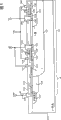
Fig. 6 is the figure that the structure of the HV-MOS relevant with embodiment 1 is shown, and is the enlarged drawing of the HV-MOS11 among Fig. 4.To attached with prosign with the same key element shown in Fig. 4.But, in the figure, in order to seek the convenience of later explanation, compare with Fig. 4 make about opposite the description.
At n
-Form the 1st dielectric film LA on the layer 110.On the upper surface of the 1st dielectric film LA and at n
-Layer 110 top forms a plurality of the 1st field plate FA (FA1~FA8) that floats.Moreover floating the 1st forms the 2nd dielectric film LB on the field plate FA.On the upper surface of the 2nd dielectric film LB and at n
-Layer 110 top forms a plurality of the 2nd field plate FB (FB1~FB8) that floats.
At this, to be called " the 1st direction " towards the direction of the 2nd semiconductor region (is p trap 111 at this) from the 3rd semiconductor region (is n district 117 at this) in this manual, the thickness direction of the 1st dielectric film LA, the 2nd dielectric film LB will be called " the 2nd direction " (with reference to arrow of Fig. 6).The 1st float field plate FA1~FA8 on the 1st direction abreast the configuration, the 2nd float field plate FB1~FB8 also on the 1st identical direction abreast the configuration.
In addition, drain electrode 119 has the position DA that extends on the 1st dielectric film LA, and this part plays the function of common (not being floating state) field plate.Below, this position is called " the 1st DA of drain electrode portion ".On the other hand, gate electrode 116 has at position GA that extends on the 1st dielectric film LA and the position GB that extends on the 2nd dielectric film LB, and this part also plays the function of common field plate.Below, both are called " the 1st GA of gate electrode portion " and " the 2nd GB of gate electrode portion ".
The 1st field plate FA and the 2nd field plate FB that floats that floats utilizes the field plate effect to promote n
-The expansion of the depletion layer in the layer 110.Each the 1st field plate FA and the 2nd field plate FB that floats that floats carries out capacitive coupling mutually through the 2nd dielectric film LB, has formed a plurality of capacitors.In addition, the 2nd of the most close leakage side field plate FB1 that floats has formed capacitor between the 2nd dielectric film LB and the 1st DA of drain electrode portion, the 1st of the most close grid side float field plate FA8 through the 2nd dielectric film LB and the 2nd GB of gate electrode portion between formed capacitor.These a plurality of capacitors are shared when the partition of HV-MOS and are remained on the high voltage that applies between the drain electrode 119-source electrode 114, determine each the 1st float current potential of field plate FB of field plate FA and the 2nd of floating thus.Suppressed excessively to promote the situation of the expansion of depletion layer thus because of the field plate effect.
For example, suppose that the 1st field plate FA that floats is 1 continuous field plate, then excessively promote the expansion of depletion layer, produce electric field near the surface of silicon substrate of leaking to concentrate, high withstand voltageization of the HV-MOS difficulty that becomes.Therefore, in the present embodiment,, suppress the hyper expanded of depletion layer, high withstand voltageization of having sought HV-MOS by on the 1st direction, disposing a plurality of the 1st field plate FA and the 2nd field plate FB that floats that floats respectively abreast.
In addition, in the HV-MOS of Fig. 6, use so-called RESURF structure and seek further high withstand voltageization.That is, by to n
-Layer 110 and p
-Pn knot (hereinafter referred to as " 1pn knot ") between district's 200 (the 4th semiconductor regions) applies and compares n
-The reverse voltage that the breakdown potential of the pn knot (hereinafter referred to as " 2pn knot ") between layer 110 and the p trap 111 is forced down makes n
-The impurity concentration of layer 110 reduces and reduced thickness arrives following degree, that is, and and the n between n district 117 and p trap 111
-Depletion layer expands to the degree of the upper surface of substrate in the layer 110 from the 1pn knot.
In the present embodiment, be decided to be a, the 1st field plate FA and the 2nd that floats is floated the distance of the 2nd direction (thickness direction of the 2nd dielectric film LB) between the field plate FB when being decided to be b at thickness the 1st dielectric film LA, compare with existing structure, thicken the 1st dielectric film LA, attenuate the 2nd dielectric film LB makes a〉b.
Fig. 7 is illustrated among the HV-MOS of Fig. 6 to make 114 short circuits of gate electrode 116-source electrode, make this HV-MOS become the figure of the Electric Field Distribution of partition state, this HV-MOS inside when 114 at drain electrode 119-source electrode has applied high voltage.In the figure, show from surface of silicon (Si surface) and play n district 117 and p
-The Electric Field Distribution of the pn junction depth between the district 200.Particularly solid line shows the Electric Field Distribution and the n of surface of silicon
-Layer 110 and p
-The Electric Field Distribution of the 1pn junction depth between the district 200.On the other hand, Fig. 8 be illustrate existing HV-MOS (in Fig. 6, a<b, and, connected float field plate FB1 of drain electrode 119 and the 2nd) in the figure of the same Electric Field Distribution of Fig. 7.
From Fig. 7, Fig. 8 as can be known, the position that electric field strength is the highest is near the part of leakage in the 1pn junction depth.Thereby, become this part as the breakdown critical electric field point at position of the withstand voltage of decision HV-MOS.On the other hand, on the surface of silicon below the front end of the 1st GA of gate electrode portion and the 1st float field plate FA1~FA8 leakage lateral edges separately below or the beneath at source edge to peak electric field (electric field is concentrated).
As shown in Figure 8, in the HV-MOS of existing structure, the peak electric field of surface of silicon is bigger, and is very little with poor (tolerance limit) of the electric field strength of breakdown critical electric field point.Thereby, when the use of reality, because the cause of the influence of the coating coating insulating film that forms or the polarization of epoxy resin, the peak electric field of surface of silicon surpass the electric field strength of breakdown critical electric field point easily, may there be the problem of unstable of withstand voltage decline or voltage endurance on HV-MOS.
Different therewith, the peak electric field of surface of silicon is smaller in the present embodiment shown in Figure 7 as can be known.That is, electric field concentrates quilt to be relaxed as can be known.Thereby, increased for the tolerance limit of the electric field strength of breakdown critical electric field point, because the peak electric field of surface of silicon is difficult to surpass the electric field strength of breakdown critical electric field point, so can suppress the problem of unstable of withstand voltage decline or voltage endurance.Its result, HV-MOS can stably keep high withstand voltage.
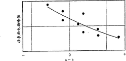
Fig. 9 is the relation of the peak electric field of a-b and surface of silicon.The value of a-b is big more as can be known, and peak electric field is more little.That is,, tolerance limit can be increased, above-mentioned effect can be increased for the electric field strength of breakdown critical electric field point by increasing thickness a, reducing the value that distance b further increases a-b.
Moreover Figure 10 is illustrated under the partition state of HV-MOS of Fig. 6 the Potential distribution in 114 at drain electrode 119-source electrode has applied this HV-MOS of high-tension situation and the figure of CURRENT DISTRIBUTION.Potential distribution illustrates with equipotential line, and its shape is with corresponding to the shape of the expansion of leaking the side depletion layer from source.On the other hand, Figure 11 shows existing HV-MOS (that is Potential distribution and the CURRENT DISTRIBUTION same with Figure 10 among a<b) in Fig. 6.
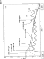
Reference numbering 0~6 among Figure 10 and Figure 11 shows surface of silicon (n
-The interval of the equipotential line the interface of layer the 110 and the 1st dielectric film LA).In the HV-MOS relevant with present embodiment, because the thickness a of the 1st dielectric film LA is big, so as shown in Figure 10, because the distortion of equipotential line is relaxed in the 1st dielectric film LA, so compare with existing Figure 11,0~6 size becomes impartial at interval.This point has shown that in the HV-MOS of present embodiment the expansion with near existing structure is compared surface of silicon depletion layer is uniform.If the expansion of depletion layer becomes evenly, then be difficult to produce electric field and concentrate, therefore, in the HV-MOS of present embodiment, can suppress the size of the peak electric field of surface of silicon lower.Like this, can observe the effect of using Fig. 7 to illustrate according to the Potential distribution of Figure 10.
In addition, Figure 12 shows the field plate FA, the 2nd that floats of the 1st when having applied high voltage between source-leakages of the HV-MOS that cuts off state and floats and distribute between the leakage-source of potential difference of each capacitor maintenance of forming between field plate FB, the 1st DA of drain electrode portion, the 1st GA of gate electrode portion, the 2nd GB of gate electrode portion.In Figure 12, the curve chart of solid line is the curve chart of the distribution among the HV-MOS of Fig. 6 relevant with present embodiment, and dotted line is the curve chart of the distribution among the existing HV-MOS (in Fig. 6, a<b, and connected drain electrode 119 and the 2nd field plate FB1 that floats).In the HV-MOS of existing structure, in the capacitor that approaches source and leakage side, there is the trend that keeps extra high voltage, so may there be the insulation breakdown of the 2nd dielectric film LB in this part.As shown in Figure 12, in the HV-MOS of present embodiment, this trend diminishes, and the discrete of potential difference that each capacitor keeps reduced.That is,, can obtain being difficult to producing the effect of the insulation breakdown of the 2nd dielectric film LB, thus, also can help high withstand voltageization of HV-MOS according to present embodiment.
In addition, in the HV-MOS of present embodiment, compare with existing structure, owing to reduced the 1st distance b that field plate FA and the 2nd floats the thickness direction (the 2nd direction) between the field plate FB of floating, so increased the capacitance of each capacitor.Thereby, owing to the capacitance coupling effect in each capacitor has improved, so promoted the polarization of the 2nd dielectric film LB.In existing structure, though n
-The depletion layer on layer 110 top each the 1st float field plate FA below expansion easily, but each the 1st float between the field plate FA below have the trend be difficult to expand.But, in the present embodiment, cause because of the high capacitance coupling effect in each capacitor, the 2nd dielectric film LB is polarized, because the cause of this influence, even can obtain each the 1st float between the field plate FA below depletion layer also easily the expansion effect, thus, also can help high withstand voltageization of HV-MOS.
As above illustrating, the present invention can be applicable to have the semiconductor device of RESURF structure.Thus, compare, can seek further high withstand voltageization with existing RESURF structure.In addition, also can be applicable to n
-Layer 110 has made the so-called multilayer RESURF structure (for example, No. the 4422089th, United States Patent (USP)) of the mutually different sandwich construction of impurity concentration.
In addition, in the above description, show the example that applies the present invention to MOSFET, but application of the present invention is not limited thereto, for example also can be widely used in diode or IGBT etc.Figure 13 illustrates the figure that embodiment 1 is applied to the example of high withstand voltage diode (HV-diode), is the enlarged drawing of the HV-diode 14 among Fig. 5.Since to attached with prosign with the same key element shown in Fig. 5 and Fig. 6, Therefore, omited the detailed explanation here.Have again, in the figure, in order to seek the convenience of later explanation, compare with Fig. 5 make about opposite the description.
In addition, as mentioned above, in HV-diode 14, because n
-Layer 143 plays the function of the 1st semiconductor region, p
+The function of the 2nd semiconductor region is played in anode region 144, and n layer 121 plays the function of the 3rd semiconductor region, so " the 1st direction " of this situation is towards p from n layer 121
+The direction of anode region 144 (with reference to the arrow of Figure 13).
In this HV-diode 14, also used so-called RESURF structure.That is, by to n
-Layer 143 and p
-1pn knot between district's 200 (the 4th semiconductor regions) applies and compares n
-Layer 143 and p
+The reverse voltage that the breakdown potential of the 2pn knot between the anode region 144 is forced down makes n
-The impurity concentration of layer 143 reduces and reduced thickness arrives following degree, that is, and and at n layer 121 and p
+N between the anode region 144
-Depletion layer expands to the degree of the upper surface of substrate in the layer 143 from the 1pn knot.
In the HV-of Figure 13 diode, be decided to be a, the 1st field plate FA and the 2nd that floats is floated the distance of the 2nd direction between the field plate FB when being decided to be b at thickness, compare, also thicken the 1st dielectric film LA with existing structure with the 1st dielectric film LA, attenuate the 2nd dielectric film LB makes a〉b.At a〉in the HV-diode of b, aspect following, also can obtain and above-mentioned same effect: promptly, reduced the peak electric field of surface of silicon, relaxed electric field and concentrated, can suppress the problem of unstable of withstand voltage decline or voltage endurance etc.
<embodiment 2 〉
Figure 14 is the figure that the structure of the HV-MOS relevant with embodiment 2 is shown.With the difference of HV-MOS shown in Figure 6 in embodiment 1 be that drain electrode 119 has the position DB that extends on the 2nd dielectric film LB.This position DB plays the function of common (not being floating state) field plate, below, be called " the 2nd DB of drain electrode portion ".
As shown in Figure 14, the length in the upwardly extending part of the 1st side above the 2nd dielectric film LB in the 2nd DB of drain electrode portion is longer than the length in the upwardly extending part of the 1st side on the 1st dielectric film LA in the 1st DA of drain electrode portion.The 2nd DB of drain electrode portion has covered the 1st DA of drain electrode portion through the 2nd dielectric film LB.And the part of the 2nd DB of drain electrode portion is overlapping through the float part of field plate FA1 of the 2nd dielectric film LB and the 1st.That is, as shown in Figure 14, we can say that also the 2nd DB of drain electrode portion is connected to the 2nd field plate FB1 that floats on the drain electrode 119 of Fig. 6.
Figure 15 is illustrated among the HV-MOS of Figure 14 to make 114 short circuits of gate electrode 116-source electrode, make this HV-MOS become the figure of the Electric Field Distribution of partition state, this HV-MOS inside when 114 at drain electrode 119-source electrode has applied high voltage.In the figure, show from surface of silicon (Si surface) and play n district 117 and p
-The Electric Field Distribution of the pn junction depth between the district 200.Particularly solid line shows the Electric Field Distribution and the n of surface of silicon
-Layer 110 and p
-The Electric Field Distribution of the 1pn junction depth between the district 200.
Figure 15 with at the Fig. 7 shown in the embodiment 1 more as can be known, according to present embodiment, the peak electric field that the 1st of the most close leakage side in the surface of silicon is floated below the edge part of field plate FA1 is relaxed.Because because of near the electric field strength of the cause breakdown critical electric field point of this influence (leaking the part of 1pn junction depth in the n district 117 of side) has reduced, historical facts or anecdotes has showed high withstand voltageization of HV-MOS.That is,, compare, can realize further high withstand voltageization with embodiment 1 according to present embodiment.
In addition, Figure 16 shows the field plate FA, the 2nd that floats of the 1st when having applied high voltage between source-leakages of the HV-MOS that cuts off state and floats and distribute between the leakage-source of potential difference of each capacitor maintenance of forming between field plate FB, the 1st DA of drain electrode portion, the 1st GA of gate electrode portion, the 2nd GB of gate electrode portion.In Figure 16, the curve chart of solid line is the curve chart of the distribution among the HV-MOS of Figure 14 relevant with present embodiment, dotted line be existing HV-MOS (in Figure 14, the curve chart of the distribution among a<b).As can be known in the present embodiment, also similarly to Example 1, the discrete of potential difference that each capacitor keeps reduced.That is, in the present embodiment, also be difficult to produce the insulation breakdown of the 2nd dielectric film LB, can help high withstand voltageization of HV-MOS.
<embodiment 3 〉
Figure 17 is the figure that the structure of the HV-MOS relevant with embodiment 3 is shown.In the figure, because to attached with prosign with the same key element shown in Fig. 6 and Figure 14, the detailed explanation of these key elements of Therefore, omited.
In the present embodiment, each the 1st width and the 1st of floating field plate FA mutual interval of field plate FA of floating is equated.That is, each the 1st is being floated the 1st direction of field plate FA (from n district 117 towards n
+The direction in source region 112) width is decided to be i, when each the 1st distance of floating the 1st direction between field plate FA is decided to be j, i=j.In addition, in the example of Figure 17, the relation and the existing structure of thickness a (thickness of the 1st dielectric film LA) and distance b (the 1st float field plate FA and the 2nd float the distance of the 2nd direction between the field plate FB) are identical, are decided to be a<b.Aspect beyond above-mentioned be same at the Figure 14 shown in the embodiment 2.
Figure 18 is illustrated among the HV-MOS of Figure 17 to make 114 short circuits of gate electrode 116-source electrode, make this HV-MOS become the figure of the Electric Field Distribution of partition state, the HV-MOS inside when 114 at drain electrode 119-source electrode has applied high voltage.In the figure, show from surface of silicon (Si surface) and play n district 117 and p
-The Electric Field Distribution of the pn junction depth between the district 200.Particularly solid line shows the Electric Field Distribution and the n of surface of silicon
-Layer 110 and p
-The Electric Field Distribution of the 1pn junction depth between the district 200.With the Fig. 8 of Electric Field Distribution among the HV-MOS that existing structure is shown more as can be known, in Figure 18 of present embodiment, the peak electric field step-down in the surface of silicon, electric field are concentrated and have been relaxed.Thereby, increased for the tolerance limit of the electric field strength of breakdown critical electric field point, because the peak electric field of surface of silicon is difficult to surpass the electric field strength of breakdown critical electric field point, so can suppress the problem of unstable of withstand voltage decline or voltage endurance.Its result, HV-MOS can stably keep high withstand voltage.
Figure 19 is illustrated under the partition state of HV-MOS of Figure 17 the Potential distribution in 114 at drain electrode 119-source electrode has applied this HV-MOS of high-tension situation and the figure of CURRENT DISTRIBUTION.In Figure 19, Potential distribution also illustrates with equipotential line, shows surface of silicon (n with reference to numbering 0~6
-The interval of the equipotential line the interface of layer the 110 and the 1st dielectric film LA).In the present embodiment, because each the 1st width and the 1st of floating field plate FA mutual width of field plate FA of floating is equated, so compare the size at interval 0~6 equalization that becomes with existing Figure 11.That is, the expansion with near existing structure is compared surface of silicon depletion layer in the HV-MOS of present embodiment is uniformly, the size of the peak electric field in this part can be suppressed lower.Like this, can observe above-mentioned effect according to the Potential distribution of Figure 19.
Have again, in Figure 17, the relation of thickness a and distance b is decided to be a<b, but but also Application Example 1 is decided to be a b.At this moment, also can obtain the effect that in embodiment 1, illustrated, can realize further high withstand voltageization.
In addition, in the present embodiment, show the example that applies the present invention to MOSFET, but application of the present invention is not limited thereto, for example also can be widely used in diode or IGBT etc.
<embodiment 4 〉
Figure 20 is the figure that the structure of the HV-MOS relevant with embodiment 4 is shown.In the figure, because to attached with prosign with the same key element shown in Fig. 6 and Figure 14, the detailed explanation of these key elements of Therefore, omited.
The HV-MOS relevant with present embodiment also has a plurality of the 3rd field plate FC (FC1~FC6) that floats that floats the 3rd dielectric film LC that forms on the field plate FB and form the 2nd thereon except the structure of the HV-MOS of Fig. 6.At n
-The top of floor 110 in the 1st direction (from n district 117 towards n
+The direction in source region 112) disposed the 3rd field plate FC that floats abreast.And, if the thickness of the 1st dielectric film LA is decided to be a, the 1st the float distance of the 2nd direction (thickness direction of the 1st dielectric film LA, the 2nd dielectric film LB, the 3rd dielectric film LC) between the field plate FB of field plate FA and the 2nd of floating is decided to be b, the 2nd the float distance of the 2nd direction between the field plate FC of field plate FB and the 3rd of floating is decided to be c, then reduced distance c so that c<a and c<b (attenuate the 3rd dielectric film LC).In the example of Figure 20, identical with existing structure, be decided to be a<b.
In addition, drain electrode 119 has the position DC that extends on the 3rd dielectric film LC.This position DC plays the function of common (not being floating state) field plate, below, this position is called " the 3rd DC of drain electrode portion ".On the other hand, source electrode 114 has the position SC that extends on the 3rd dielectric film LC.This position SC plays the function of common field plate, below, this position is called " source electrode part SC ".
Figure 21 is illustrated among the HV-MOS of Figure 20 to make 114 short circuits of gate electrode 116-source electrode, make this HV-MOS become the figure of the Electric Field Distribution of partition state, the HV-MOS inside when 114 at drain electrode 119-source electrode has applied high voltage.In the figure, show from surface of silicon (Si surface) and play n district 117 and p
-The Electric Field Distribution of the pn junction depth between the district 200.Particularly solid line shows the Electric Field Distribution and the n of surface of silicon
-Layer 110 and p
-The Electric Field Distribution of the 1pn junction depth between the district 200.With the Fig. 8 of Electric Field Distribution among the HV-MOS that existing structure is shown more as can be known, in Figure 21, the peak electric field step-down in the surface of silicon, electric field are concentrated and have been relaxed.Thereby, increased for the tolerance limit of the electric field strength of breakdown critical electric field point, because the peak electric field of surface of silicon is difficult to surpass the electric field strength of breakdown critical electric field point, so can suppress the problem of unstable of withstand voltage decline or voltage endurance.Its result, HV-MOS can stably keep high withstand voltage.
Figure 22 is illustrated under the partition state of HV-MOS of Figure 20 the Potential distribution in 114 at drain electrode 119-source electrode has applied this HV-MOS of high-tension situation and the figure of CURRENT DISTRIBUTION.In Figure 22, Potential distribution also illustrates with equipotential line, shows surface of silicon (n with reference to numbering 0~6
-The interval of the equipotential line the interface of layer the 110 and the 1st dielectric film LA).Compare with existing Figure 11, the equipotential line in the surface of silicon moves towards leaking lateral deviation, expands easily at the surface of silicon depletion layer as can be known.This has shown the situation of the peak electric field step-down of surface of silicon.Like this, can observe above-mentioned effect according to the Potential distribution of Figure 22.
In addition, in the HV-MOS of present embodiment, owing to reduced above-mentioned distance c, so increased by the 2nd the float capacitance of each capacitor that field plate FC, the 2nd DB of drain electrode portion, source electrode part SC form of field plate FB, the 3rd of floating.Thereby, owing to the capacitance coupling effect in each capacitor has improved, so promoted the polarization of the 3rd dielectric film LC.Because the cause of this influence, though can obtain depletion layer in the past is difficult to expand each the 1st float between the field plate FA below the also effect of expansion easily of depletion layer, thus, also can help high withstand voltageization of HV-MOS.
Have again, in Figure 20, the relation of thickness a and distance b is decided to be a<b, but but also Application Example 1 as shown in Figure 23, is decided to be a b.At this moment, also can obtain the effect that in embodiment 1, illustrated, can realize further high withstand voltageization.
Figure 24 is illustrated among the HV-MOS of Figure 23 to make 114 short circuits of gate electrode 116-source electrode, make HV-MOS become the figure of the Electric Field Distribution of partition state, the HV-MOS inside when 114 at drain electrode 119-source electrode has applied high voltage.In the figure, show from surface of silicon (Si surface) and play n district 117 and p
-The Electric Field Distribution of the pn junction depth between the district 200.Particularly solid line shows the Electric Field Distribution and the n of surface of silicon
-Layer 110 and p
-The Electric Field Distribution of the 1pn junction depth between the district 200.With Figure 21 more as can be known, the peak electric field step-down in the surface of silicon, electric field are concentrated and have been relaxed.
Figure 25 is illustrated in the Potential distribution in 114 HV-MOS that apply high-tension situation of drain electrode 119-source electrode and the figure of CURRENT DISTRIBUTION under the partition state of HV-MOS of Figure 23.Potential distribution also illustrates with equipotential line, shows the interval of the equipotential line in the surface of silicon with reference to numbering 0~6.In the HV-MOS of Figure 23, because the thickness a of the 1st dielectric film LA is big, the distortion of equipotential line is relaxed in the 1st dielectric film LA, so compare with Figure 22,0~6 size becomes impartial at interval.Therefore, the size of the peak electric field in the surface of silicon can be suppressed lower.
Like this, by Application Example 1, can realize further high withstand voltageization.In addition, in the above description, show the example that applies the present invention to MOSFET, but application of the present invention is not limited thereto, for example also can be widely used in diode or IGBT etc.
<embodiment 5 〉
Figure 26 is the figure that the structure of the HV-MOS relevant with embodiment 5 is shown.In the figure, because to attached with prosign with the same key element shown in Fig. 6 and Figure 14, the detailed explanation of these key elements of Therefore, omited.
In the present embodiment, compare, widened the 1st the float width of field plate FB of field plate FA and the 2nd of floating with existing structure.That is, if each the 1st width of floating among the field plate FA through the 1st direction of the 2nd dielectric film LB and 1 the 2nd overlapping part of field plate FB of floating is decided to be g, each the 2nd distance of floating the 1st direction between field plate FB is decided to be h, g then〉h (with reference to Figure 26).
In addition, in the example of Figure 26, the relation and the existing structure of thickness a (thickness of the 1st dielectric film LA) and distance b (the 1st float field plate FA and the 2nd float the distance of the 2nd direction between the field plate FB) are identical, are decided to be a<b.
Aspect beyond above-mentioned be same at the Figure 14 shown in the embodiment 2.
According to present embodiment, because the 1st the float width of the overlapping part of field plate FB of field plate FA and the 2nd of floating is wide, so bigger than the capacitance of existing structure with the 1st the float capacitance of each capacitor of field plate FB formation of field plate FA and the 2nd of floating.Thereby, owing to the capacitance coupling effect in each capacitor has improved, so promoted the polarization of the 2nd dielectric film LB.Thus, though can obtain each the 1st float between the field plate FA below the also effect of expansion easily of depletion layer, can help high withstand voltageization of HV-MOS.
In addition, by improving the capacitance coupling effect in each capacitor, discrete having reduced between leak in the source of the potential difference that each capacitor keeps also can obtain being difficult to producing the effect of the insulation breakdown of the 2nd dielectric film LB.
In addition, in the present embodiment, show the example that applies the present invention to MOSFET, but application of the present invention is not limited thereto, for example also can be widely used in diode or IGBT etc.
<embodiment 6 〉
Figure 27 is the figure that the structure of the HV-MOS relevant with embodiment 6 is shown.In the figure, because to attached with prosign with the same key element shown in Figure 20, the detailed explanation of these key elements of Therefore, omited.
The HV-MOS of Figure 27 has removed the 1st field plate FA that floats from the structure of Figure 20.Be decided to be a, b respectively, the 2nd field plate FB and the 3rd that floats is floated the distance of the 2nd direction between the field plate FC when being decided to be c, a+b at the thickness with the 1st dielectric film LA and the 2nd dielectric film LB c.That is, the 2nd of Figure 27 the field plate FB and the 3rd field plate FC that floats that floats plays field plate FA and the 2nd same function of field plate FB of floating of floating with the 1st of embodiment 1 (Fig. 6) respectively.Thereby HV-MOS can stably keep high withstand voltage similarly to Example 1.
In addition, drain electrode 119 has the 1st DA of drain electrode portion that extends on the 1st dielectric film LA.The 1st DA of drain electrode portion extends on the 1st direction on the 1st dielectric film LA, and its part is overlapping through the float part of field plate FB1 of the 2nd dielectric film LB and the 2nd.Moreover, among the 3rd DC of drain electrode portion above the 1st dielectric film LA and the upwardly extending length of the 1st side than among the 1st DA of drain electrode portion on the 1st dielectric film LA and long in the upwardly extending length of the 1st side, and, than among the 2nd DB of drain electrode portion above the 1st dielectric film LA and long in the upwardly extending length of the 1st side.That is, the 3rd DC of drain electrode portion covers the top of the 1st DA of drain electrode portion and the 2nd DB of drain electrode portion.
Figure 28 is illustrated among the HV-MOS of Figure 27 to make 114 short circuits of gate electrode 116-source electrode, make HV-MOS become the figure of the Electric Field Distribution of partition state, this HV-MOS inside when 114 at drain electrode 119-source electrode has applied high voltage.In the figure, show from surface of silicon (Si surface) and play n district 117 and p
-The Electric Field Distribution of the pn junction depth between the district 200.Particularly solid line shows the Electric Field Distribution and the n of surface of silicon
-Layer 110 and p
-The Electric Field Distribution of the 1pn junction depth between the district 200.Similarly to Example 1, the peak electric field step-down in the surface of silicon, electric field are concentrated and have been relaxed as can be known.
In addition, the peak electric field of the most close leakage side in the surface of silicon is to float under the edge of leakage side of field plate FB2 the 2nd, and floating the 2nd peak value do not occur under the edge of field plate FB1.This is because the 1st DA of drain electrode portion that plays the function of common field plate extends to and the 2nd floats on a part of position overlapped of field plate FB1.In addition, because the 3rd DC of drain electrode portion extends above the 1st dielectric film LA more longways,, concentrate so further relaxed near the electric field of the drain electrode in the surface of silicon so that cover the top of the 1st DA of drain electrode portion and the 2nd DB of drain electrode portion.Thereby because near the electric field strength step-down of breakdown critical electric field point (part of the 1pn junction depth in the n district 117 of leakage side), the withstand voltage of HV-MOS has improved.That is,, compare, can realize further high withstand voltageization with embodiment 1 according to present embodiment.
Figure 29 illustrates the figure that embodiment 2 is applied to the variation of present embodiment.That is, with Figure 27 the difference of structure be that drain electrode has the 2nd DB of drain electrode portion that extends on the 2nd dielectric film LB.As shown in Figure 29, among the 2nd DB of drain electrode portion above the 1st dielectric film LA and the upwardly extending part of the 1st side than among the 1st DA of drain electrode portion on the 1st dielectric film LA and long in the upwardly extending length of the 1st side.That is, the 2nd DB of drain electrode portion has covered the top of the 1st DA of drain electrode portion through the 2nd dielectric film LB.As shown in Figure 29, also we can say drain electrode 119 and the 2nd that the 2nd DB of drain electrode portion the has connected Figure 27 field plate FB1 that floats.
Figure 30 is illustrated among the HV-MOS of Figure 29 to make 114 short circuits of gate electrode 116-source electrode, make HV-MOS become the figure of the Electric Field Distribution of partition state, this HV-MOS inside when 114 at drain electrode 119-source electrode has applied high voltage.In Figure 30, also same with Figure 28, the peak electric field of the most close leakage side in the surface of silicon is to float under the edge of leakage side of field plate FB2 the 2nd, and floating the 2nd peak value do not occur under the edge of field plate FB1.So, because near the electric field strength step-down of breakdown critical electric field point, so the withstand voltage of HV-MOS has improved.That is,, can realize further high withstand voltageization according to this variation.
In addition, in the present embodiment, show the example that applies the present invention to MOSFET, but application of the present invention is not limited thereto, for example also can be widely used in diode or IGBT etc.
<embodiment 7 〉
Figure 31 is the figure that the structure of the HV-MOS relevant with embodiment 7 is shown.In the figure, because to attached with prosign with the same key element shown in Figure 20, the detailed explanation of these key elements of Therefore, omited.
In the HV-MOS relevant with embodiment, in addition, drain electrode 119 has at the 1st DA of drain electrode portion that extends on the 1st dielectric film LA and the 2nd DB of drain electrode portion that extends on the 2nd dielectric film LB.And, comparing with existing structure, the 1st DA of drain electrode portion and the 2nd DB of drain electrode portion extend longlyer.As shown in Figure 31, if the length in the upwardly extending part of the 1st side on the 1st dielectric film LA among the 1st DA of drain electrode portion is decided to be d, then above the 1st dielectric film LA and in the length of the upwardly extending part of the 1st side, Duoed length e among the 2nd DB of drain electrode portion than length d.At this moment, make length d enough big, so that d〉e.In addition, in the example of Figure 31, the thickness a and the 1st of the 1st dielectric film LA field plate FA and the 2nd that floats floats between the field plate FB identically along the relation and the existing structure of the distance b of the 2nd direction, is decided to be a<b.As shown in Figure 31, we can say that also the 1st DA of drain electrode portion is connected to the 1st with the drain electrode 119 of Fig. 6 and floats on the field plate FA1, the 2nd DB of drain electrode portion is connected to the 2nd float field plate FB1, FB2 on the drain electrode 119 of Fig. 6.
Figure 32 is illustrated among the HV-MOS of Figure 31 to make 114 short circuits of gate electrode 116-source electrode, make HV-MOS become the figure of the Electric Field Distribution of partition state, the HV-MOS inside when 114 at drain electrode 119-source electrode has applied high voltage.In the figure, show from surface of silicon (Si surface) and play n district 117 and p
-The Electric Field Distribution of the pn junction depth between the district 200.Particularly solid line shows the Electric Field Distribution and the n of surface of silicon
-Layer 110 and p
-The Electric Field Distribution of the 1pn junction depth between the district 200.Surface of silicon the peak electric field of the most close leakage side be to float under the edge of leakage side of field plate FA2 the 1st.
For example, wait more as can be known with Fig. 7, according to present embodiment, the peak electric field of the most close leakage side is far away from breakdown critical electric field point (part of the 1pn junction depth in the n district 117 of leakage side).So, near the electric field strength step-down of breakdown critical electric field point, the withstand voltage of HV-MOS has improved.
Have again, in Figure 31, the relation of thickness a and distance b is decided to be a<b, but but also Application Example 1 as shown in Figure 33, is decided to be a b.Figure 34 is illustrated among the HV-MOS of Figure 33 to make 114 short circuits of gate electrode 116-source electrode, make HV-MOS become the figure of the Electric Field Distribution of partition state, the HV-MOS inside when 114 at drain electrode 119-source electrode has applied high voltage.In the figure, show from surface of silicon (Si surface) and play n district 117 and p
-The Electric Field Distribution of the pn junction depth between the district 200.Particularly solid line shows the Electric Field Distribution and the n of surface of silicon
-Layer 110 and p
-The Electric Field Distribution of the 1pn junction depth between the district 200.Generally speaking, compare with Figure 32, the peak electric field step-down in the surface of silicon, electric field are concentrated and have been relaxed as can be known.Thereby, if Application Example 1 then can realize further high withstand voltageization.
In addition, application of the present invention is not limited to MOSFET, for example also can be widely used in diode or IGBT etc.Figure 35 illustrates the figure that present embodiment is applied to the example of high withstand voltage diode (HV-diode), is the enlarged drawing of the HV-diode 14 among Fig. 5.Since to attached with prosign with the same key element shown in Fig. 5 and Figure 13, Therefore, omited the detailed explanation here.Have again, even in the figure, in order to seek the convenience of later explanation, also compare with Fig. 5 make about opposite the description.(structure of a in the Figure 13 shown in the embodiment 1<b) similarly makes the 1st CA of cathode electrode portion and the 2nd CB of cathode electrode portion extend longlyer with the 1st DA of drain electrode portion and the 2nd DB of drain electrode portion of Figure 31 to the HV-diode of Figure 35 with respect to existing HV-diode.
Figure 36 is the figure of the Electric Field Distribution in this HV-diode that is illustrated in the HV-diode of Figure 35 when cathode electrode 142 and 145 of anode electrodes have applied reverse voltage.In the figure, show from surface of silicon (Si surface) and play n district 117 and p
-The Electric Field Distribution of the pn junction depth between the district 200.Particularly solid line shows the Electric Field Distribution and the n of surface of silicon
-Layer 143 and p
-The Electric Field Distribution of the 1pn junction depth between the district 200.In addition, the figure shows Electric Field Distribution in the C-C section (that is the bight on high potential island) of Fig. 3.The peak electric field of close cathode side in the surface of silicon is to float under the edge of cathode side of field plate FA2 the 1st, and near the electric field strength of breakdown critical electric field point (part of the 1pn junction depth of the n layer 121 of cathode side) has reduced.
On the other hand, Figure 37 illustrates in the existing HV-diode (structure of a<b in the Figure 13 shown in the embodiment 1) and the figure same Electric Field Distribution of Figure 36.This figure also illustrates the Electric Field Distribution in the C-C section (that is the bight on high potential island) of Fig. 3.The peak electric field of close cathode side in the surface of silicon is the 2nd floating under the edge of leakage side of field plate FB1 of not having in Figure 35.
Relatively Figure 36 and Figure 37 as can be known, according to present embodiment, the peak electric field of close cathode side is far away from breakdown critical electric field point.So, near the situation height of the HV-diode of the electric field ratio Figure 35 the breakdown critical electric field point.Thereby the HV-diode of having used Figure 35 of present embodiment can obtain high withstand voltage.
In general, at place, the bight on high potential island, because of the influence of its shape, the trend that exists particularly the peak electric field in the surface of silicon of the cathode side (under the situation at HV-MOS, being to leak side) of HV-diode to uprise.For example, the peak electric field of also observing the most close cathode side in the surface of silicon in Figure 37 is bigger than the peak electric field of the most close anode-side.Therefore, may there be the situation that uprises the withstand voltage decline that causes because of HV-diode or near the electric field strength the breakdown critical electric field point among the HV-MOS in bight formation in the past.According to present embodiment, owing to can suppress near the electric field strength the breakdown critical electric field point among HV-diode or the HV-MOS lower, so effective especially under the situation of HV-diode that is applied to the bight or HV-MOS.
<embodiment 8 〉
In embodiment 8, the example that embodiment 7 is applied to embodiment 6 is shown.Figure 38 is the figure that the structure of the HV-MOS relevant with present embodiment is shown.In the figure, because to attached with prosign with the same key element shown in Fig. 6 and Figure 29, the detailed explanation of these key elements of Therefore, omited.
The HV-MOS relevant with present embodiment makes the 1st DA of drain electrode portion, the 2nd DB of drain electrode portion, the 3rd DC of drain electrode portion extend longlyer respectively with respect to the structure of Figure 29.As shown in Figure 38, if will on the 1st dielectric film LA and in the length of the upwardly extending part of the 1st side, be decided to be d among the 1st DA of drain electrode portion, then above the 1st dielectric film LA and in the length of the upwardly extending part of the 1st side, Duoed length e among the 2nd DB of drain electrode portion than length d.And, among the 3rd DC of drain electrode portion above the 1st dielectric film LA and more than the length length d+e of the upwardly extending part of the 1st side length f.At this moment, make length d enough big, so that make d〉e and d〉f.
As shown in Figure 38, we can say that also the 2nd DB of drain electrode portion is connected to the 2nd with the drain electrode 119 of Figure 29 and floats on field plate FB1, the FB2, in addition, the 3rd DC of drain electrode portion is connected to the 3rd field plate FC1 that floats on the drain electrode 119 of Figure 29.
Figure 39 is illustrated among the HV-MOS of Figure 38 to make 114 short circuits of gate electrode 116-source electrode, make HV-MOS become the figure of the Electric Field Distribution of partition state, the HV-MOS inside when 114 at drain electrode 119-source electrode has applied high voltage.In the figure, show from surface of silicon (Si surface) and play n district 117 and p
-The Electric Field Distribution of the pn junction depth between the district 200.Particularly solid line shows the Electric Field Distribution and the n of surface of silicon
-Layer 110 and p
-The Electric Field Distribution of the 1pn junction depth between the district 200.Surface of silicon the peak electric field of the most close leakage side be to float under the edge of leakage side of field plate FB3 the 2nd.With Figure 30 more as can be known, in the present embodiment, also similarly to Example 7, the peak electric field of the most close leakage side is far away from breakdown critical electric field point (leaking the part of 1pn junction depth in the n district 117 of side).So, near the electric field strength step-down of breakdown critical electric field point, the withstand voltage of HV-MOS has improved.
As mentioned above, at place, the bight on high potential island, the situation of consequent withstand voltage decline may take place in the trend that exists particularly the peak electric field in the surface of silicon of the cathode side (under the situation at HV-MOS, being to leak side) of HV-diode to uprise.According to present embodiment, owing to can suppress near the electric field strength the breakdown critical electric field point of HV-diode or HV-MOS lower, so effective especially under the situation of the HV-in the bight that is applied to high potential island diode.
<variation 〉
In each above embodiment, applied the present invention to use the transversal device of RESURF structure, but the present invention also can be applicable to vertical device.In the variation that this illustrate the foregoing description 1 is applied to vertical device.
Figure 40 is the chip vertical view of vertical HV-MOS, and Figure 41 is the amplification profile along the D-D line of its chip peripheral part (marginal end portion).In Figure 40 and Figure 41, attached with prosign to same key element.In addition, also attached with the key element of the same function of Fig. 6 in two figure with the symbol identical with it to having.
As shown in Figure 40, in vertical HV-MOS, source of configuration electrode 114 and gate electrode 116 on the upper surface of chip, side configuration drain electrode (not shown) overleaf.On the peripheral part of the upper surface of chip, form raceway groove and stop to distinguish 211 (with reference to Figure 41), form electrode 212 (being called " raceway groove stops region electrode ") thereon.
In vertical HV-MOS, different with the horizontal HV-MOS that in embodiment 1~8, has illustrated, at n
+Form n on the substrate 220 as the 1st semiconductor region
-Layer 210.That is, at n
-Layer does not form p 210 times
-District's (the 4th semiconductor region).n
+Substrate 211 plays the function of the leakage of HV-MOS, at n
+The back side one side of substrate 211 forms drain electrode 221.At n
-Form the p trap 111 as the 2nd semiconductor region in the layer 210, portion forms p within it
+District 113.The gate electrode 116 that forms through the 1st dielectric film LA above p trap 111 is at p trap 111 and p
+Source electrode 114 is formed at the top in district 113.And, at n
-The raceway groove that forms as the 3rd semiconductor region on the chip peripheral part of floor 210 stops to distinguish 211, forms raceway groove thereon and stops region electrode 212.To clamp n
-The mode of floor 210 forms p trap 111 and raceway groove stops to distinguish 211.
Stop n between the region electrode 212 at the wiring portion of gate electrode 116 and raceway groove
-Layer 210 top the 1st dielectric film LA forms a plurality of the 1st field plate FA that floats.Moreover floating the 1st forms the 2nd dielectric film LB on the field plate FA, forms a plurality of the 2nd field plate FB that floats on the 2nd dielectric film LB.As shown in Figure 41, on the 1st direction of the 2nd semiconductor region (p trap 111), dispose the 1st field plate FA and the 2nd field plate FB (among Figure 40, simplified the 1st field plate FA, the 2nd field plate FB that floats that floats and described) that floats that floats respectively abreast from the 3rd semiconductor region (raceway groove stops to distinguish 211).
In this variation, similarly to Example 1, be decided to be a, the 1st field plate FA and the 2nd that floats is floated the distance of the 2nd direction (thickness direction of the 1st dielectric film LA and the 2nd dielectric film LB) between the field plate FB when being decided to be b at thickness the 1st dielectric film LA, compare with existing structure, thicken the 1st dielectric film LA, attenuate the 2nd dielectric film LB makes a〉b.
Like this, by embodiment 1 is applied to vertical HV-MOS, the 1st dielectric film LA and n when having relaxed the partition of this HV-MOS
-The electric field at the interface of layer 210 is concentrated.Thereby this HV-MOS can stably keep high withstand voltage at the chip peripheral part, high withstand voltageization that can seek vertical HV-MOS.
Have again, show the example that applies the present invention to vertical HV-MOS, but in addition, also can be applicable to the whole of vertical power device such as IGBT or diode, can obtain same effect at this.In addition, in this variation, only show the situation of having used embodiment 1, but also can use other embodiment certainly.
Claims (26)
1. semiconductor device possesses:
The 1st semiconductor region of the 1st conduction type;
The 3rd semiconductor region of the 1st conduction type that the 2nd semiconductor region of the 2nd conduction type that forms in the mode of clamping above-mentioned the 1st semiconductor region and its impurity concentration are higher than the impurity concentration of above-mentioned the 1st semiconductor region;
The 1st dielectric film that on above-mentioned the 1st semiconductor region, forms;
The a plurality of the 1st field plate of floating that on above-mentioned the 1st dielectric film, forms, the above-mentioned a plurality of the 1st field plate of floating is being configured in above above-mentioned the 1st semiconductor region side by side from above-mentioned the 3rd semiconductor region on the 1st direction of above-mentioned the 2nd semiconductor region;
At the above-mentioned the 1st the 2nd dielectric film of floating and forming on the field plate;
Form on above-mentioned the 2nd dielectric film and above above-mentioned the 1st semiconductor region on above-mentioned the 1st direction and a plurality of the 2nd field plate of floating of row arrangement;
At the above-mentioned the 2nd the 3rd dielectric film of floating and forming on the field plate; And
Be formed on the field plate of floating of a plurality of the 3rd on above-mentioned the 3rd dielectric film, the above-mentioned a plurality of the 3rd field plate of floating is being configured in above above-mentioned the 1st semiconductor region on above-mentioned the 1st direction side by side.
2. semiconductor device as claimed in claim 1, it is characterized in that: be decided to be a, the above-mentioned the 1st field plate and the above-mentioned the 2nd of floating is floated between the field plate when being decided to be b as the distance on the 2nd direction of above-mentioned thickness direction a at the thickness with above-mentioned the 1st dielectric film b.
3. semiconductor device as claimed in claim 1 is characterized in that:
Also have the electrode that on above-mentioned the 3rd semiconductor region, forms,
Above-mentioned electrode has in the 1st electrode part of extending on above-mentioned the 1st dielectric film and the 2nd electrode part of extending on above-mentioned the 2nd dielectric film,
The length that extends the part above above-mentioned the 1st dielectric film in above-mentioned the 2nd electrode part on above-mentioned the 1st direction is than long in the length that extends the part on above-mentioned the 1st dielectric film on above-mentioned the 1st direction in above-mentioned the 1st electrode part.
4. the semiconductor device described in claim 1 is characterized in that:
Be decided to be a, the above-mentioned the 2nd field plate and the above-mentioned the 3rd of floating is floated between the field plate when the distance of above-mentioned the 2nd direction is decided to be c a at the thickness with above-mentioned the 1st dielectric film c.
5. as each the described semiconductor device in the claim 1~4, it is characterized in that:
Above-mentioned the 2nd semiconductor region plays the function of transistorized channel region,
Above-mentioned the 3rd semiconductor region plays the function in above-mentioned transistorized drain region.
6. as each described semiconductor device in the claim 1~4, it is characterized in that:
Above-mentioned the 2nd semiconductor region plays the function of the anode of diode,
Above-mentioned the 3rd semiconductor region plays the function of the negative electrode of above-mentioned diode.
7. as each described semiconductor device in the claim 1~4, it is characterized in that:
The function that the raceway groove that above-mentioned the 3rd semiconductor region plays the peripheral part of chip stops to distinguish.
8. as each described semiconductor device in the claim 1~4, it is characterized in that:
Also has the 4th semiconductor region with the 2nd conduction type of the following side contacts of above-mentioned the 1st semiconductor region.
9. semiconductor device as claimed in claim 8 is characterized in that:
Low and the thin thickness of the impurity concentration of above-mentioned the 1st semiconductor region, so that by the knot of the 1pn between above-mentioned the 1st semiconductor region and above-mentioned the 4th semiconductor region is applied the reverse voltage that forces down than the breakdown potential of the knot of the 2pn between above-mentioned the 1st semiconductor region and above-mentioned the 2nd semiconductor region, between above-mentioned the 2nd semiconductor region and above-mentioned the 3rd semiconductor region, make depletion layer expand to the upper surface of above-mentioned the 1st semiconductor region from above-mentioned 1pn knot.
10. semiconductor device possesses:
The 1st semiconductor region of the 1st conduction type;
The 3rd semiconductor region of the 1st conduction type that the 2nd semiconductor region of the 2nd conduction type that forms in the mode of clamping above-mentioned the 1st semiconductor region and its impurity concentration are higher than the impurity concentration of above-mentioned the 1st semiconductor region;
The electrode that on above-mentioned the 3rd semiconductor region, forms;
The 1st dielectric film that on above-mentioned the 1st semiconductor region, forms;
The 2nd dielectric film that on above-mentioned the 1st dielectric film, forms;
Be formed on the field plate of floating of a plurality of the 2nd on above-mentioned the 2nd dielectric film, the above-mentioned a plurality of the 2nd field plate of floating is being configured in above above-mentioned the 1st semiconductor region side by side from above-mentioned the 3rd semiconductor region on the 1st direction of above-mentioned the 2nd semiconductor region;
At the above-mentioned the 2nd the 3rd dielectric film of floating and forming on the field plate; And
Be formed on the field plate of floating of a plurality of the 3rd on above-mentioned the 3rd dielectric film, the above-mentioned a plurality of the 3rd field plate of floating is being configured in above above-mentioned the 1st semiconductor region on above-mentioned the 1st direction side by side,
Wherein, above-mentioned electrode has the 1st electrode part that above-mentioned the 1st direction is extended in above-mentioned the 1st dielectric film upper edge.
11. semiconductor device as claimed in claim 10 is characterized in that:
Above-mentioned electrode also has in the 2nd electrode part of extending on above-mentioned the 2nd dielectric film and the 3rd electrode part of extending on above-mentioned the 3rd dielectric film,
The length that extends the part above above-mentioned the 1st dielectric film in above-mentioned the 3rd electrode part on above-mentioned the 1st direction is than long in the length that extends the part on above-mentioned the 1st dielectric film on above-mentioned the 1st direction in above-mentioned the 1st electrode part, and than long in the length that extends the part above above-mentioned the 1st dielectric film on above-mentioned the 1st direction in above-mentioned the 2nd electrode part.
12. semiconductor device as claimed in claim 10 is characterized in that:
Be decided to be a, the thickness of above-mentioned the 2nd dielectric film is decided to be b, the above-mentioned the 2nd field plate and the above-mentioned the 3rd of floating is floated between the field plate when being decided to be c as the distance on the 2nd direction of above-mentioned thickness direction a+b at the thickness with above-mentioned the 1st dielectric film c.
13. each the described semiconductor device as in the claim 10~12 is characterized in that:
Above-mentioned the 2nd semiconductor region plays the function of transistorized channel region,
Above-mentioned the 3rd semiconductor region plays the function in above-mentioned transistorized drain region.
14. each the described semiconductor device as in the claim 10~12 is characterized in that:
Above-mentioned the 2nd semiconductor region plays the function of the anode of diode,
Above-mentioned the 3rd semiconductor region plays the function of the negative electrode of above-mentioned diode.
15. each the described semiconductor device as in the claim 10~12 is characterized in that:
The function that the raceway groove that above-mentioned the 3rd semiconductor region plays the peripheral part of chip stops to distinguish.
16. each the described semiconductor device as in the claim 10~12 is characterized in that:
Also has the 4th semiconductor region with the 2nd conduction type of the following side contacts of above-mentioned the 1st semiconductor region.
17. semiconductor device as claimed in claim 16 is characterized in that:
Low and the thin thickness of the impurity concentration of above-mentioned the 1st semiconductor region, so that by the knot of the 1pn between above-mentioned the 1st semiconductor region and above-mentioned the 4th semiconductor region is applied the reverse voltage that forces down than the breakdown potential of the knot of the 2pn between above-mentioned the 1st semiconductor region and above-mentioned the 2nd semiconductor region, between above-mentioned the 2nd semiconductor region and above-mentioned the 3rd semiconductor region, make depletion layer expand to the upper surface of above-mentioned the 1st semiconductor region from above-mentioned 1pn knot.
18. a semiconductor device possesses:
The 1st semiconductor region of the 1st conduction type;
The 3rd semiconductor region of the 1st conduction type that the 2nd semiconductor region of the 2nd conduction type that forms in the mode of clamping above-mentioned the 1st semiconductor region and its impurity concentration are higher than the impurity concentration of above-mentioned the 1st semiconductor region;
The electrode that on above-mentioned the 3rd semiconductor region, forms;
The 1st dielectric film that on above-mentioned the 1st semiconductor region, forms;
The 2nd dielectric film that on above-mentioned the 1st dielectric film, forms;
Be formed on the field plate of floating of a plurality of the 2nd on above-mentioned the 2nd dielectric film, the above-mentioned a plurality of the 2nd field plate of floating is being configured in above above-mentioned the 1st semiconductor region side by side from above-mentioned the 3rd semiconductor region on the 1st direction of above-mentioned the 2nd semiconductor region;
At the above-mentioned the 2nd the 3rd dielectric film of floating and forming on the field plate; And
Be formed on the field plate of floating of a plurality of the 3rd on above-mentioned the 3rd dielectric film, the above-mentioned a plurality of the 3rd field plate of floating is being configured in above above-mentioned the 1st semiconductor region on above-mentioned the 1st direction side by side, wherein,
Above-mentioned electrode has in the 1st electrode part of extending on above-mentioned the 1st dielectric film and the 2nd electrode part of extending on above-mentioned the 2nd dielectric film,
The length that extends the part above above-mentioned the 1st dielectric film in above-mentioned the 2nd electrode part on above-mentioned the 1st direction is than long in the length that extends the part on above-mentioned the 1st dielectric film on above-mentioned the 1st direction in above-mentioned the 1st electrode part.
19. semiconductor device as claimed in claim 18 is characterized in that:
Above-mentioned electrode also has the 3rd electrode part of extending on above-mentioned the 3rd dielectric film,
The length that extends the part above above-mentioned the 1st dielectric film in above-mentioned the 3rd electrode part on above-mentioned the 1st direction is than longer in the length that extends the part above above-mentioned the 1st dielectric film on above-mentioned the 1st direction in above-mentioned the 2nd electrode part.
20. semiconductor device as claimed in claim 19 is characterized in that:
The length that in above-mentioned the 1st electrode part, on above-mentioned the 1st direction, extends the part on above-mentioned the 1st dielectric film be decided to be the length that on above-mentioned the 1st direction, extends the part above above-mentioned the 1st dielectric film in d, above-mentioned the 2nd electrode part be decided to be Duoed the length that on above-mentioned the 1st direction, extends the part above above-mentioned the 1st dielectric film in length e, above-mentioned the 3rd electrode part than above-mentioned length d and be decided to be than above-mentioned length d+e also during multiple-length f d e and d f.
21. semiconductor device as claimed in claim 18 is characterized in that:
Be decided to be a, the thickness of above-mentioned the 2nd dielectric film is decided to be b, the above-mentioned the 2nd field plate and the above-mentioned the 3rd of floating is floated between the field plate when being decided to be c as the distance on the 2nd direction of above-mentioned thickness direction a+b at the thickness with above-mentioned the 1st dielectric film c.
22. each the described semiconductor device as in the claim 18~21 is characterized in that:
Above-mentioned the 2nd semiconductor region plays the function of transistorized channel region,
Above-mentioned the 3rd semiconductor region plays the function in above-mentioned transistorized drain region.
23., it is characterized in that as each described semiconductor device in the claim 18~21:
Above-mentioned the 2nd semiconductor region plays the function of the anode of diode,
Above-mentioned the 3rd semiconductor region plays the function of the negative electrode of above-mentioned diode.
24., it is characterized in that as each described semiconductor device in the claim 18~21:
The function that the raceway groove that above-mentioned the 3rd semiconductor region plays the peripheral part of chip stops to distinguish.
25., it is characterized in that as each described semiconductor device in the claim 18~21:
Also has the 4th semiconductor region with the 2nd conduction type of the following side contacts of above-mentioned the 1st semiconductor region.
26. semiconductor device as claimed in claim 25 is characterized in that:
Low and the thin thickness of the impurity concentration of above-mentioned the 1st semiconductor region, so that by the knot of the 1pn between above-mentioned the 1st semiconductor region and above-mentioned the 4th semiconductor region is applied the reverse voltage that forces down than the breakdown potential of the knot of the 2pn between above-mentioned the 1st semiconductor region and above-mentioned the 2nd semiconductor region, between above-mentioned the 2nd semiconductor region and above-mentioned the 3rd semiconductor region, make depletion layer expand to the upper surface of above-mentioned the 1st semiconductor region from above-mentioned 1pn knot.
Applications Claiming Priority (2)
| Application Number | Priority Date | Filing Date | Title |
|---|---|---|---|
| JP2004016663A JP4731816B2 (en) | 2004-01-26 | 2004-01-26 | Semiconductor device |
| JP016663/2004 | 2004-01-26 |
Publications (2)
| Publication Number | Publication Date |
|---|---|
| CN1649168A CN1649168A (en) | 2005-08-03 |
| CN100472803C true CN100472803C (en) | 2009-03-25 |
Family
ID=34792485
Family Applications (1)
| Application Number | Title | Priority Date | Filing Date |
|---|---|---|---|
| CNB2004100114776A Active CN100472803C (en) | 2004-01-26 | 2004-12-31 | Semiconductor device |
Country Status (6)
| Country | Link |
|---|---|
| US (1) | US7122875B2 (en) |
| JP (1) | JP4731816B2 (en) |
| KR (1) | KR100639692B1 (en) |
| CN (1) | CN100472803C (en) |
| DE (1) | DE102004059620B4 (en) |
| TW (1) | TWI253177B (en) |
Families Citing this family (59)
| Publication number | Priority date | Publication date | Assignee | Title |
|---|---|---|---|---|
| US7679111B2 (en) * | 2005-09-16 | 2010-03-16 | International Rectifier Corporation | Termination structure for a power semiconductor device |
| JP2007318062A (en) * | 2006-04-27 | 2007-12-06 | Matsushita Electric Ind Co Ltd | High withstand voltage semiconductor switching device |
| JP4935192B2 (en) * | 2006-05-31 | 2012-05-23 | 三菱電機株式会社 | Semiconductor device |
| JP5512287B2 (en) * | 2007-02-22 | 2014-06-04 | フォルシュングスフェアブント ベルリン エー ファウ | Semiconductor device and manufacturing method thereof |
| US9484451B2 (en) | 2007-10-05 | 2016-11-01 | Vishay-Siliconix | MOSFET active area and edge termination area charge balance |
| US20090096039A1 (en) * | 2007-10-10 | 2009-04-16 | United Microelectronics Corp. | High-voltage device and manufacturing method of top layer in high-voltage device |
| JP5312889B2 (en) * | 2008-09-29 | 2013-10-09 | ローム株式会社 | Semiconductor device |
| JP5371358B2 (en) * | 2008-09-29 | 2013-12-18 | ローム株式会社 | Semiconductor device and manufacturing method of semiconductor device |
| JP5487851B2 (en) * | 2008-09-30 | 2014-05-14 | サンケン電気株式会社 | Semiconductor device |
| CN101414637B (en) * | 2008-12-01 | 2010-08-25 | 西安电子科技大学 | Groove insulation cross-over gate heterojunction field effect transistor |
| WO2010067430A1 (en) | 2008-12-10 | 2010-06-17 | トヨタ自動車株式会社 | Semiconductor device |
| JP5391447B2 (en) | 2009-04-06 | 2014-01-15 | 三菱電機株式会社 | Semiconductor device and manufacturing method thereof |
| JP5376365B2 (en) * | 2009-04-16 | 2013-12-25 | 三菱電機株式会社 | Semiconductor device |
| JP5460279B2 (en) * | 2009-12-11 | 2014-04-02 | 株式会社日立製作所 | Semiconductor device and manufacturing method thereof |
| JP5517688B2 (en) * | 2010-03-24 | 2014-06-11 | 三菱電機株式会社 | Semiconductor device |
| JP5594515B2 (en) * | 2010-03-26 | 2014-09-24 | 日本電気株式会社 | Semiconductor device, electronic device, method for manufacturing semiconductor device, and method for operating semiconductor device |
| US8546889B2 (en) | 2010-06-04 | 2013-10-01 | Fuji Electric Co., Ltd. | Semiconductor device and driving circuit |
| JP5601072B2 (en) * | 2010-08-03 | 2014-10-08 | サンケン電気株式会社 | Semiconductor device |
| JP2012134198A (en) * | 2010-12-20 | 2012-07-12 | Mitsubishi Electric Corp | Semiconductor device and manufacturing method of the same |
| JP5703829B2 (en) * | 2011-02-24 | 2015-04-22 | サンケン電気株式会社 | Semiconductor device |
| JP5716591B2 (en) * | 2011-07-26 | 2015-05-13 | 三菱電機株式会社 | Semiconductor device |
| JP5979836B2 (en) | 2011-09-09 | 2016-08-31 | ルネサスエレクトロニクス株式会社 | Semiconductor device and manufacturing method of semiconductor device |
| US9093432B2 (en) | 2011-09-23 | 2015-07-28 | Sanken Electric Co., Ltd. | Semiconductor device |
| DE112011105785B4 (en) | 2011-10-26 | 2015-05-13 | Toyota Jidosha Kabushiki Kaisha | Semiconductor device |
| US9431249B2 (en) | 2011-12-01 | 2016-08-30 | Vishay-Siliconix | Edge termination for super junction MOSFET devices |
| WO2013105350A1 (en) | 2012-01-12 | 2013-07-18 | トヨタ自動車株式会社 | Semiconductor device and method of manufacturing thereof |
| US9614043B2 (en) | 2012-02-09 | 2017-04-04 | Vishay-Siliconix | MOSFET termination trench |
| US9842911B2 (en) * | 2012-05-30 | 2017-12-12 | Vishay-Siliconix | Adaptive charge balanced edge termination |
| US20130334648A1 (en) * | 2012-06-15 | 2013-12-19 | Taiwan Semiconductor Manufacturing Company, Ltd. | Methods and Apparatus for High Voltage Diodes |
| US20140001479A1 (en) * | 2012-06-29 | 2014-01-02 | Power Integrations, Inc. | Switching device with charge distribution structure |
| US9245879B2 (en) | 2012-06-29 | 2016-01-26 | Power Integrations, Inc. | Static discharge system |
| US10192981B2 (en) | 2012-06-29 | 2019-01-29 | Power Integrations, Inc. | Switching device with charge distribution structure |
| US10224923B2 (en) * | 2012-10-31 | 2019-03-05 | Nxp Usa, Inc. | Method and apparatus for driving a power transistor gate |
| JP6030923B2 (en) * | 2012-11-09 | 2016-11-24 | シャープ株式会社 | Semiconductor device and manufacturing method thereof |
| CN102945839B (en) * | 2012-12-06 | 2015-09-16 | 电子科技大学 | A kind of high voltage interconnection structure of part field plate shielding |
| JP6009341B2 (en) * | 2012-12-13 | 2016-10-19 | ルネサスエレクトロニクス株式会社 | Semiconductor device |
| JP6101183B2 (en) | 2013-06-20 | 2017-03-22 | 株式会社東芝 | Semiconductor device |
| JP6168961B2 (en) * | 2013-10-10 | 2017-07-26 | 三菱電機株式会社 | Semiconductor device |
| CN103779407B (en) * | 2014-01-20 | 2016-05-18 | 西安电子科技大学 | Add source field plate depletion-mode AlGaN/GaN HEMT device architecture and preparation method thereof |
| CN103779408B (en) * | 2014-01-20 | 2016-08-17 | 西安电子科技大学 | Based on depletion type groove grid AlGaN/GaN HEMT device structure and preparation method thereof |
| JP2015177041A (en) * | 2014-03-14 | 2015-10-05 | 株式会社東芝 | semiconductor device |
| JP6210913B2 (en) * | 2014-03-20 | 2017-10-11 | ルネサスエレクトロニクス株式会社 | Semiconductor device |
| US9508596B2 (en) | 2014-06-20 | 2016-11-29 | Vishay-Siliconix | Processes used in fabricating a metal-insulator-semiconductor field effect transistor |
| US9887259B2 (en) | 2014-06-23 | 2018-02-06 | Vishay-Siliconix | Modulated super junction power MOSFET devices |
| US9882044B2 (en) | 2014-08-19 | 2018-01-30 | Vishay-Siliconix | Edge termination for super-junction MOSFETs |
| JP6052481B2 (en) * | 2014-12-25 | 2016-12-27 | 富士電機株式会社 | Semiconductor device |
| CN106653830B (en) * | 2015-10-28 | 2019-09-17 | 无锡华润上华科技有限公司 | Semiconductor devices pressure-resistance structure |
| JP6690336B2 (en) * | 2016-03-18 | 2020-04-28 | 富士電機株式会社 | Semiconductor device |
| CN107710408B (en) * | 2016-05-26 | 2021-06-18 | 新电元工业株式会社 | Semiconductor device with a plurality of semiconductor chips |
| JP2018157008A (en) * | 2017-03-16 | 2018-10-04 | サンケン電気株式会社 | Semiconductor device |
| US10262938B2 (en) * | 2017-08-31 | 2019-04-16 | Vanguard International Semiconductor Corporation | Semiconductor structure having conductive layer overlapping field oxide |
| CN107887432B (en) * | 2017-10-30 | 2020-02-14 | 济南大学 | Lateral insulated gate bipolar transistor with charge-adjustable field plate |
| CN107680997B (en) * | 2017-10-30 | 2020-04-14 | 济南大学 | Lateral double-diffusion metal oxide semiconductor field effect transistor with adjustable field plate |
| JP7160167B2 (en) * | 2018-12-28 | 2022-10-25 | 三菱電機株式会社 | semiconductor equipment |
| CN109713032B (en) * | 2018-12-28 | 2020-12-18 | 电子科技大学 | Terminal structure of anti-radiation semiconductor device |
| JP7459703B2 (en) * | 2020-07-15 | 2024-04-02 | 富士電機株式会社 | Semiconductor Device |
| JP2022144785A (en) * | 2021-03-19 | 2022-10-03 | 株式会社東芝 | Semiconductor device |
| CN113707717B (en) * | 2021-08-31 | 2023-09-15 | 电子科技大学 | Power device with multiple floating field plates and collector PMOS structure |
| CN115224113B (en) * | 2022-09-15 | 2023-01-20 | 北京芯可鉴科技有限公司 | Transverse super junction device, transverse insulated gate bipolar transistor and manufacturing method |
Citations (3)
| Publication number | Priority date | Publication date | Assignee | Title |
|---|---|---|---|---|
| US4766474A (en) * | 1980-05-30 | 1988-08-23 | Sharp Kabushiki Kiasha | High voltage MOS transistor |
| US6246101B1 (en) * | 1998-07-07 | 2001-06-12 | Mitsubishi Denki Kabushiki Kaisha | Isolation structure and semiconductor device including the isolation structure |
| US6307232B1 (en) * | 1997-06-06 | 2001-10-23 | Mitsubishi Denki Kabushiki Kaisha | Semiconductor device having lateral high breakdown voltage element |
Family Cites Families (7)
| Publication number | Priority date | Publication date | Assignee | Title |
|---|---|---|---|---|
| CA1131801A (en) * | 1978-01-18 | 1982-09-14 | Johannes A. Appels | Semiconductor device |
| JPS56169369A (en) * | 1980-05-30 | 1981-12-26 | Sharp Corp | High withstand voltage mos field effect semiconductor device |
| JP3906504B2 (en) * | 1996-11-27 | 2007-04-18 | 株式会社デンソー | Isolated semiconductor device |
| JP3905981B2 (en) * | 1998-06-30 | 2007-04-18 | 株式会社東芝 | High voltage semiconductor device |
| JP2001196578A (en) * | 1999-10-29 | 2001-07-19 | Sanyo Electric Co Ltd | Semiconductor device and manufacturing method therefor |
| JP2002353444A (en) * | 2001-05-28 | 2002-12-06 | Fuji Electric Co Ltd | Semiconductor device |
| JP3654872B2 (en) | 2001-06-04 | 2005-06-02 | 松下電器産業株式会社 | High voltage semiconductor device |
-
2004
- 2004-01-26 JP JP2004016663A patent/JP4731816B2/en not_active Expired - Lifetime
- 2004-10-28 TW TW093132685A patent/TWI253177B/en active
- 2004-11-30 US US10/998,983 patent/US7122875B2/en active Active
- 2004-12-10 DE DE102004059620A patent/DE102004059620B4/en active Active
- 2004-12-31 CN CNB2004100114776A patent/CN100472803C/en active Active
-
2005
- 2005-01-20 KR KR1020050005308A patent/KR100639692B1/en active IP Right Grant
Patent Citations (3)
| Publication number | Priority date | Publication date | Assignee | Title |
|---|---|---|---|---|
| US4766474A (en) * | 1980-05-30 | 1988-08-23 | Sharp Kabushiki Kiasha | High voltage MOS transistor |
| US6307232B1 (en) * | 1997-06-06 | 2001-10-23 | Mitsubishi Denki Kabushiki Kaisha | Semiconductor device having lateral high breakdown voltage element |
| US6246101B1 (en) * | 1998-07-07 | 2001-06-12 | Mitsubishi Denki Kabushiki Kaisha | Isolation structure and semiconductor device including the isolation structure |
Also Published As
| Publication number | Publication date |
|---|---|
| KR20050077015A (en) | 2005-07-29 |
| US20050161761A1 (en) | 2005-07-28 |
| JP4731816B2 (en) | 2011-07-27 |
| KR100639692B1 (en) | 2006-10-31 |
| DE102004059620A1 (en) | 2005-08-18 |
| US7122875B2 (en) | 2006-10-17 |
| TWI253177B (en) | 2006-04-11 |
| DE102004059620B4 (en) | 2011-07-28 |
| JP2005209983A (en) | 2005-08-04 |
| TW200525761A (en) | 2005-08-01 |
| CN1649168A (en) | 2005-08-03 |
Similar Documents
| Publication | Publication Date | Title |
|---|---|---|
| CN100472803C (en) | Semiconductor device | |
| US8253163B2 (en) | High voltage semiconductor device including a free wheel diode | |
| US9515067B2 (en) | Semiconductor device having switching element and free wheel diode and method for controlling the same | |
| CN102034873B (en) | Thin film transistor and method for manufacturing the same | |
| WO2017130597A1 (en) | Semiconductor device | |
| US20020053717A1 (en) | Semiconductor apparatus | |
| US20140299916A1 (en) | Monolithic cell for an integrated circuit and especially a monolithic switching cell | |
| EP2260514A1 (en) | A semiconductor device wherein a first insulated gate field effect transistor is connected in series with a second field effect transistor | |
| CN104157648A (en) | Semiconductor device having switching element and free wheel diode and method for controlling the same | |
| JP5269852B2 (en) | Semiconductor device | |
| CN100580928C (en) | Composite field effect transistor structure and manufacturing method thereof | |
| CN110690278B (en) | Insulated gate bipolar transistor and preparation method thereof | |
| JP4334395B2 (en) | Semiconductor device | |
| CN101521203B (en) | Semiconductor transverse device and high-voltage device | |
| GB2295052A (en) | Integrated circuits | |
| CN101521213B (en) | Dielectric separation type semiconductor device, its manufacture method and integrated circuit device | |
| US6339243B1 (en) | High voltage device and method for fabricating the same | |
| CN106992212A (en) | The transistor device of gate leakage capacitance with increase | |
| CN105336788B (en) | Semiconductor devices | |
| US20170170310A1 (en) | Semiconductor device and manufacturing method of the semiconductor device | |
| JPH1093023A (en) | Semiconductor device | |
| US20220231164A1 (en) | Switching element | |
| CN109616522A (en) | A kind of lateral high-voltage device | |
| US20220190155A1 (en) | Semiconductor device | |
| US20220020875A1 (en) | Semiconductor device |
Legal Events
| Date | Code | Title | Description |
|---|---|---|---|
| C06 | Publication | ||
| PB01 | Publication | ||
| C10 | Entry into substantive examination | ||
| SE01 | Entry into force of request for substantive examination | ||
| C14 | Grant of patent or utility model | ||
| GR01 | Patent grant |