KR20070085879A - Light-emitting device - Google Patents
Light-emitting device Download PDFInfo
- Publication number
- KR20070085879A KR20070085879A KR1020077012875A KR20077012875A KR20070085879A KR 20070085879 A KR20070085879 A KR 20070085879A KR 1020077012875 A KR1020077012875 A KR 1020077012875A KR 20077012875 A KR20077012875 A KR 20077012875A KR 20070085879 A KR20070085879 A KR 20070085879A
- Authority
- KR
- South Korea
- Prior art keywords
- light emitting
- film
- amorphous oxide
- layer
- effect transistor
- Prior art date
Links
- 230000005669 field effect Effects 0.000 claims abstract description 49
- 238000000034 method Methods 0.000 claims description 133
- 239000000758 substrate Substances 0.000 claims description 112
- 108091006149 Electron carriers Proteins 0.000 claims description 74
- 239000004065 semiconductor Substances 0.000 claims description 38
- 229910052738 indium Inorganic materials 0.000 claims description 22
- 229910052725 zinc Inorganic materials 0.000 claims description 20
- 230000001965 increasing effect Effects 0.000 claims description 17
- 229910052718 tin Inorganic materials 0.000 claims description 16
- 229910052733 gallium Inorganic materials 0.000 claims description 6
- 239000011159 matrix material Substances 0.000 claims description 6
- 108091008695 photoreceptors Proteins 0.000 claims description 4
- 239000010408 film Substances 0.000 description 238
- 239000010410 layer Substances 0.000 description 221
- 239000001301 oxygen Substances 0.000 description 85
- 229910052760 oxygen Inorganic materials 0.000 description 85
- QVGXLLKOCUKJST-UHFFFAOYSA-N atomic oxygen Chemical compound [O] QVGXLLKOCUKJST-UHFFFAOYSA-N 0.000 description 78
- 239000010409 thin film Substances 0.000 description 66
- 239000008186 active pharmaceutical agent Substances 0.000 description 46
- 230000015572 biosynthetic process Effects 0.000 description 42
- 238000005401 electroluminescence Methods 0.000 description 39
- 238000004549 pulsed laser deposition Methods 0.000 description 36
- 239000000203 mixture Substances 0.000 description 32
- 239000011521 glass Substances 0.000 description 25
- 238000000151 deposition Methods 0.000 description 24
- 239000000463 material Substances 0.000 description 24
- LFQSCWFLJHTTHZ-UHFFFAOYSA-N Ethanol Chemical compound CCO LFQSCWFLJHTTHZ-UHFFFAOYSA-N 0.000 description 22
- 239000012212 insulator Substances 0.000 description 22
- 238000004519 manufacturing process Methods 0.000 description 20
- 239000010931 gold Substances 0.000 description 17
- 150000001875 compounds Chemical class 0.000 description 15
- -1 Li-added Al Inorganic materials 0.000 description 14
- 239000013078 crystal Substances 0.000 description 14
- PCHJSUWPFVWCPO-UHFFFAOYSA-N gold Chemical compound [Au] PCHJSUWPFVWCPO-UHFFFAOYSA-N 0.000 description 14
- 229910052737 gold Inorganic materials 0.000 description 14
- 238000000206 photolithography Methods 0.000 description 14
- 229920000139 polyethylene terephthalate Polymers 0.000 description 14
- 239000005020 polyethylene terephthalate Substances 0.000 description 14
- 230000008021 deposition Effects 0.000 description 13
- CSCPPACGZOOCGX-UHFFFAOYSA-N Acetone Chemical compound CC(C)=O CSCPPACGZOOCGX-UHFFFAOYSA-N 0.000 description 12
- 238000010586 diagram Methods 0.000 description 12
- 238000004544 sputter deposition Methods 0.000 description 12
- 230000005525 hole transport Effects 0.000 description 11
- 238000002347 injection Methods 0.000 description 11
- 239000007924 injection Substances 0.000 description 11
- 229920002799 BoPET Polymers 0.000 description 10
- 238000000235 small-angle X-ray scattering Methods 0.000 description 10
- 229910052782 aluminium Inorganic materials 0.000 description 9
- 229910052751 metal Inorganic materials 0.000 description 9
- 239000002184 metal Substances 0.000 description 9
- 230000008569 process Effects 0.000 description 9
- XKRFYHLGVUSROY-UHFFFAOYSA-N Argon Chemical compound [Ar] XKRFYHLGVUSROY-UHFFFAOYSA-N 0.000 description 8
- 238000004458 analytical method Methods 0.000 description 8
- 125000004429 atom Chemical group 0.000 description 8
- 230000008859 change Effects 0.000 description 8
- 206010021143 Hypoxia Diseases 0.000 description 7
- 239000004020 conductor Substances 0.000 description 7
- 230000007423 decrease Effects 0.000 description 7
- 239000007789 gas Substances 0.000 description 7
- 239000011229 interlayer Substances 0.000 description 7
- 229920000642 polymer Polymers 0.000 description 7
- 229910052710 silicon Inorganic materials 0.000 description 7
- 230000007547 defect Effects 0.000 description 6
- 238000005238 degreasing Methods 0.000 description 6
- 238000011156 evaluation Methods 0.000 description 6
- 229910021642 ultra pure water Inorganic materials 0.000 description 6
- 239000012498 ultrapure water Substances 0.000 description 6
- 229910004298 SiO 2 Inorganic materials 0.000 description 5
- 239000003153 chemical reaction reagent Substances 0.000 description 5
- 238000000313 electron-beam-induced deposition Methods 0.000 description 5
- 230000001939 inductive effect Effects 0.000 description 5
- 150000002500 ions Chemical class 0.000 description 5
- 238000005259 measurement Methods 0.000 description 5
- 239000012071 phase Substances 0.000 description 5
- 229920003023 plastic Polymers 0.000 description 5
- 239000004033 plastic Substances 0.000 description 5
- 238000005245 sintering Methods 0.000 description 5
- 239000002904 solvent Substances 0.000 description 5
- 238000007740 vapor deposition Methods 0.000 description 5
- 229910019092 Mg-O Inorganic materials 0.000 description 4
- 229910019395 Mg—O Inorganic materials 0.000 description 4
- 229910006404 SnO 2 Inorganic materials 0.000 description 4
- 229910052786 argon Inorganic materials 0.000 description 4
- 229910052749 magnesium Inorganic materials 0.000 description 4
- 239000002985 plastic film Substances 0.000 description 4
- 239000002994 raw material Substances 0.000 description 4
- 239000010703 silicon Substances 0.000 description 4
- 229910018072 Al 2 O 3 Inorganic materials 0.000 description 3
- IJGRMHOSHXDMSA-UHFFFAOYSA-N Atomic nitrogen Chemical compound N#N IJGRMHOSHXDMSA-UHFFFAOYSA-N 0.000 description 3
- 229910001020 Au alloy Inorganic materials 0.000 description 3
- 229910005191 Ga 2 O 3 Inorganic materials 0.000 description 3
- VYPSYNLAJGMNEJ-UHFFFAOYSA-N Silicium dioxide Chemical compound O=[Si]=O VYPSYNLAJGMNEJ-UHFFFAOYSA-N 0.000 description 3
- XUIMIQQOPSSXEZ-UHFFFAOYSA-N Silicon Chemical compound [Si] XUIMIQQOPSSXEZ-UHFFFAOYSA-N 0.000 description 3
- 229910007541 Zn O Inorganic materials 0.000 description 3
- 229910052783 alkali metal Inorganic materials 0.000 description 3
- 150000001340 alkali metals Chemical class 0.000 description 3
- 229910045601 alloy Inorganic materials 0.000 description 3
- 239000000956 alloy Substances 0.000 description 3
- 229910021417 amorphous silicon Inorganic materials 0.000 description 3
- 229910052796 boron Inorganic materials 0.000 description 3
- 238000001354 calcination Methods 0.000 description 3
- 239000003990 capacitor Substances 0.000 description 3
- 238000009837 dry grinding Methods 0.000 description 3
- 238000010894 electron beam technology Methods 0.000 description 3
- 238000005516 engineering process Methods 0.000 description 3
- 238000001704 evaporation Methods 0.000 description 3
- 229910052732 germanium Inorganic materials 0.000 description 3
- 238000010438 heat treatment Methods 0.000 description 3
- 230000031700 light absorption Effects 0.000 description 3
- 239000012528 membrane Substances 0.000 description 3
- 229910052757 nitrogen Inorganic materials 0.000 description 3
- 230000003287 optical effect Effects 0.000 description 3
- 239000012044 organic layer Substances 0.000 description 3
- 229920006255 plastic film Polymers 0.000 description 3
- 238000007639 printing Methods 0.000 description 3
- 239000000523 sample Substances 0.000 description 3
- 229910021332 silicide Inorganic materials 0.000 description 3
- 239000012808 vapor phase Substances 0.000 description 3
- VQGHOUODWALEFC-UHFFFAOYSA-N 2-phenylpyridine Chemical compound C1=CC=CC=C1C1=CC=CC=N1 VQGHOUODWALEFC-UHFFFAOYSA-N 0.000 description 2
- MYMOFIZGZYHOMD-UHFFFAOYSA-N Dioxygen Chemical compound O=O MYMOFIZGZYHOMD-UHFFFAOYSA-N 0.000 description 2
- 230000005355 Hall effect Effects 0.000 description 2
- 229910052774 Proactinium Inorganic materials 0.000 description 2
- 229910001260 Pt alloy Inorganic materials 0.000 description 2
- 239000007983 Tris buffer Substances 0.000 description 2
- 229920006266 Vinyl film Polymers 0.000 description 2
- 238000002441 X-ray diffraction Methods 0.000 description 2
- 238000002083 X-ray spectrum Methods 0.000 description 2
- 238000000862 absorption spectrum Methods 0.000 description 2
- 229910052784 alkaline earth metal Inorganic materials 0.000 description 2
- 150000001342 alkaline earth metals Chemical class 0.000 description 2
- XAGFODPZIPBFFR-UHFFFAOYSA-N aluminium Chemical compound [Al] XAGFODPZIPBFFR-UHFFFAOYSA-N 0.000 description 2
- MWPLVEDNUUSJAV-UHFFFAOYSA-N anthracene Chemical class C1=CC=CC2=CC3=CC=CC=C3C=C21 MWPLVEDNUUSJAV-UHFFFAOYSA-N 0.000 description 2
- 150000004982 aromatic amines Chemical class 0.000 description 2
- 229910052791 calcium Inorganic materials 0.000 description 2
- 239000000969 carrier Substances 0.000 description 2
- 239000000919 ceramic Substances 0.000 description 2
- 238000004140 cleaning Methods 0.000 description 2
- 229910001882 dioxygen Inorganic materials 0.000 description 2
- ZUOUZKKEUPVFJK-UHFFFAOYSA-N diphenyl Chemical compound C1=CC=CC=C1C1=CC=CC=C1 ZUOUZKKEUPVFJK-UHFFFAOYSA-N 0.000 description 2
- 238000005566 electron beam evaporation Methods 0.000 description 2
- 229910021478 group 5 element Inorganic materials 0.000 description 2
- 125000005843 halogen group Chemical group 0.000 description 2
- 230000001976 improved effect Effects 0.000 description 2
- 230000001678 irradiating effect Effects 0.000 description 2
- 229910021645 metal ion Inorganic materials 0.000 description 2
- 150000002739 metals Chemical class 0.000 description 2
- 238000002156 mixing Methods 0.000 description 2
- IBHBKWKFFTZAHE-UHFFFAOYSA-N n-[4-[4-(n-naphthalen-1-ylanilino)phenyl]phenyl]-n-phenylnaphthalen-1-amine Chemical group C1=CC=CC=C1N(C=1C2=CC=CC=C2C=CC=1)C1=CC=C(C=2C=CC(=CC=2)N(C=2C=CC=CC=2)C=2C3=CC=CC=C3C=CC=2)C=C1 IBHBKWKFFTZAHE-UHFFFAOYSA-N 0.000 description 2
- 229910052758 niobium Inorganic materials 0.000 description 2
- 150000004767 nitrides Chemical class 0.000 description 2
- 239000011347 resin Substances 0.000 description 2
- 229920005989 resin Polymers 0.000 description 2
- FVBUAEGBCNSCDD-UHFFFAOYSA-N silicide(4-) Chemical compound [Si-4] FVBUAEGBCNSCDD-UHFFFAOYSA-N 0.000 description 2
- 229910052709 silver Inorganic materials 0.000 description 2
- 239000002356 single layer Substances 0.000 description 2
- 238000001228 spectrum Methods 0.000 description 2
- 230000000087 stabilizing effect Effects 0.000 description 2
- 229910052715 tantalum Inorganic materials 0.000 description 2
- XOLBLPGZBRYERU-UHFFFAOYSA-N tin dioxide Chemical compound O=[Sn]=O XOLBLPGZBRYERU-UHFFFAOYSA-N 0.000 description 2
- 229910001887 tin oxide Inorganic materials 0.000 description 2
- 238000002834 transmittance Methods 0.000 description 2
- 229910052720 vanadium Inorganic materials 0.000 description 2
- XLYOFNOQVPJJNP-UHFFFAOYSA-N water Substances O XLYOFNOQVPJJNP-UHFFFAOYSA-N 0.000 description 2
- 229910052727 yttrium Inorganic materials 0.000 description 2
- 229910052726 zirconium Inorganic materials 0.000 description 2
- 239000002841 Lewis acid Substances 0.000 description 1
- RTAQQCXQSZGOHL-UHFFFAOYSA-N Titanium Chemical compound [Ti] RTAQQCXQSZGOHL-UHFFFAOYSA-N 0.000 description 1
- DGEZNRSVGBDHLK-UHFFFAOYSA-N [1,10]phenanthroline Chemical compound C1=CN=C2C3=NC=CC=C3C=CC2=C1 DGEZNRSVGBDHLK-UHFFFAOYSA-N 0.000 description 1
- 150000001412 amines Chemical class 0.000 description 1
- 230000004888 barrier function Effects 0.000 description 1
- 239000002585 base Substances 0.000 description 1
- 239000010953 base metal Substances 0.000 description 1
- 239000004305 biphenyl Substances 0.000 description 1
- 235000010290 biphenyl Nutrition 0.000 description 1
- 239000000872 buffer Substances 0.000 description 1
- 238000012512 characterization method Methods 0.000 description 1
- 229910052804 chromium Inorganic materials 0.000 description 1
- 229910052681 coesite Inorganic materials 0.000 description 1
- 239000002131 composite material Substances 0.000 description 1
- 239000002772 conduction electron Substances 0.000 description 1
- 229910052906 cristobalite Inorganic materials 0.000 description 1
- 238000013461 design Methods 0.000 description 1
- 238000011161 development Methods 0.000 description 1
- 229910001873 dinitrogen Inorganic materials 0.000 description 1
- 230000001747 exhibiting effect Effects 0.000 description 1
- 238000013213 extrapolation Methods 0.000 description 1
- 230000002349 favourable effect Effects 0.000 description 1
- 238000010304 firing Methods 0.000 description 1
- 229920002457 flexible plastic Polymers 0.000 description 1
- 239000003353 gold alloy Substances 0.000 description 1
- 229910021480 group 4 element Inorganic materials 0.000 description 1
- 230000006872 improvement Effects 0.000 description 1
- 239000012535 impurity Substances 0.000 description 1
- 230000000977 initiatory effect Effects 0.000 description 1
- 239000011810 insulating material Substances 0.000 description 1
- 238000009413 insulation Methods 0.000 description 1
- 238000011835 investigation Methods 0.000 description 1
- 150000002503 iridium Chemical class 0.000 description 1
- RTRAMYYYHJZWQK-UHFFFAOYSA-N iridium;2-phenylpyridine Chemical compound [Ir].C1=CC=CC=C1C1=CC=CC=N1 RTRAMYYYHJZWQK-UHFFFAOYSA-N 0.000 description 1
- 238000005304 joining Methods 0.000 description 1
- 150000007517 lewis acids Chemical class 0.000 description 1
- 239000004973 liquid crystal related substance Substances 0.000 description 1
- 238000001459 lithography Methods 0.000 description 1
- 238000004518 low pressure chemical vapour deposition Methods 0.000 description 1
- 125000001624 naphthyl group Chemical group 0.000 description 1
- 239000008239 natural water Substances 0.000 description 1
- WCPAKWJPBJAGKN-UHFFFAOYSA-N oxadiazole Chemical compound C1=CON=N1 WCPAKWJPBJAGKN-UHFFFAOYSA-N 0.000 description 1
- 239000002245 particle Substances 0.000 description 1
- IEQIEDJGQAUEQZ-UHFFFAOYSA-N phthalocyanine Chemical compound N1C(N=C2C3=CC=CC=C3C(N=C3C4=CC=CC=C4C(=N4)N3)=N2)=C(C=CC=C2)C2=C1N=C1C2=CC=CC=C2C4=N1 IEQIEDJGQAUEQZ-UHFFFAOYSA-N 0.000 description 1
- 239000000049 pigment Substances 0.000 description 1
- 238000005268 plasma chemical vapour deposition Methods 0.000 description 1
- 238000000623 plasma-assisted chemical vapour deposition Methods 0.000 description 1
- 229910021420 polycrystalline silicon Inorganic materials 0.000 description 1
- 229920001721 polyimide Polymers 0.000 description 1
- 239000010970 precious metal Substances 0.000 description 1
- 238000002360 preparation method Methods 0.000 description 1
- 229910052761 rare earth metal Inorganic materials 0.000 description 1
- 150000002910 rare earth metals Chemical class 0.000 description 1
- 238000002128 reflection high energy electron diffraction Methods 0.000 description 1
- 238000012827 research and development Methods 0.000 description 1
- 230000004044 response Effects 0.000 description 1
- 238000012552 review Methods 0.000 description 1
- 229920006395 saturated elastomer Polymers 0.000 description 1
- 239000000377 silicon dioxide Substances 0.000 description 1
- 235000012239 silicon dioxide Nutrition 0.000 description 1
- 229910052814 silicon oxide Inorganic materials 0.000 description 1
- 239000007858 starting material Substances 0.000 description 1
- 229910052682 stishovite Inorganic materials 0.000 description 1
- 239000000126 substance Substances 0.000 description 1
- 238000007725 thermal activation Methods 0.000 description 1
- 229910052719 titanium Inorganic materials 0.000 description 1
- 239000010936 titanium Substances 0.000 description 1
- 150000003852 triazoles Chemical class 0.000 description 1
- 229910052905 tridymite Inorganic materials 0.000 description 1
- 229910052721 tungsten Inorganic materials 0.000 description 1
- 238000001947 vapour-phase growth Methods 0.000 description 1
Images


Classifications
-
- H—ELECTRICITY
- H01—ELECTRIC ELEMENTS
- H01L—SEMICONDUCTOR DEVICES NOT COVERED BY CLASS H10
- H01L27/00—Devices consisting of a plurality of semiconductor or other solid-state components formed in or on a common substrate
- H01L27/02—Devices consisting of a plurality of semiconductor or other solid-state components formed in or on a common substrate including semiconductor components specially adapted for rectifying, oscillating, amplifying or switching and having potential barriers; including integrated passive circuit elements having potential barriers
- H01L27/12—Devices consisting of a plurality of semiconductor or other solid-state components formed in or on a common substrate including semiconductor components specially adapted for rectifying, oscillating, amplifying or switching and having potential barriers; including integrated passive circuit elements having potential barriers the substrate being other than a semiconductor body, e.g. an insulating body
- H01L27/1214—Devices consisting of a plurality of semiconductor or other solid-state components formed in or on a common substrate including semiconductor components specially adapted for rectifying, oscillating, amplifying or switching and having potential barriers; including integrated passive circuit elements having potential barriers the substrate being other than a semiconductor body, e.g. an insulating body comprising a plurality of TFTs formed on a non-semiconducting substrate, e.g. driving circuits for AMLCDs
- H01L27/1222—Devices consisting of a plurality of semiconductor or other solid-state components formed in or on a common substrate including semiconductor components specially adapted for rectifying, oscillating, amplifying or switching and having potential barriers; including integrated passive circuit elements having potential barriers the substrate being other than a semiconductor body, e.g. an insulating body comprising a plurality of TFTs formed on a non-semiconducting substrate, e.g. driving circuits for AMLCDs with a particular composition, shape or crystalline structure of the active layer
- H01L27/1225—Devices consisting of a plurality of semiconductor or other solid-state components formed in or on a common substrate including semiconductor components specially adapted for rectifying, oscillating, amplifying or switching and having potential barriers; including integrated passive circuit elements having potential barriers the substrate being other than a semiconductor body, e.g. an insulating body comprising a plurality of TFTs formed on a non-semiconducting substrate, e.g. driving circuits for AMLCDs with a particular composition, shape or crystalline structure of the active layer with semiconductor materials not belonging to the group IV of the periodic table, e.g. InGaZnO
-
- G—PHYSICS
- G03—PHOTOGRAPHY; CINEMATOGRAPHY; ANALOGOUS TECHNIQUES USING WAVES OTHER THAN OPTICAL WAVES; ELECTROGRAPHY; HOLOGRAPHY
- G03G—ELECTROGRAPHY; ELECTROPHOTOGRAPHY; MAGNETOGRAPHY
- G03G5/00—Recording members for original recording by exposure, e.g. to light, to heat, to electrons; Manufacture thereof; Selection of materials therefor
- G03G5/02—Charge-receiving layers
- G03G5/04—Photoconductive layers; Charge-generation layers or charge-transporting layers; Additives therefor; Binders therefor
- G03G5/08—Photoconductive layers; Charge-generation layers or charge-transporting layers; Additives therefor; Binders therefor characterised by the photoconductive material being inorganic
-
- G—PHYSICS
- G03—PHOTOGRAPHY; CINEMATOGRAPHY; ANALOGOUS TECHNIQUES USING WAVES OTHER THAN OPTICAL WAVES; ELECTROGRAPHY; HOLOGRAPHY
- G03G—ELECTROGRAPHY; ELECTROPHOTOGRAPHY; MAGNETOGRAPHY
- G03G5/00—Recording members for original recording by exposure, e.g. to light, to heat, to electrons; Manufacture thereof; Selection of materials therefor
- G03G5/14—Inert intermediate or cover layers for charge-receiving layers
- G03G5/142—Inert intermediate layers
- G03G5/144—Inert intermediate layers comprising inorganic material
-
- H—ELECTRICITY
- H01—ELECTRIC ELEMENTS
- H01L—SEMICONDUCTOR DEVICES NOT COVERED BY CLASS H10
- H01L21/00—Processes or apparatus adapted for the manufacture or treatment of semiconductor or solid state devices or of parts thereof
- H01L21/02—Manufacture or treatment of semiconductor devices or of parts thereof
- H01L21/02104—Forming layers
- H01L21/02365—Forming inorganic semiconducting materials on a substrate
- H01L21/02518—Deposited layers
- H01L21/02587—Structure
- H01L21/0259—Microstructure
- H01L21/02592—Microstructure amorphous
-
- H—ELECTRICITY
- H01—ELECTRIC ELEMENTS
- H01L—SEMICONDUCTOR DEVICES NOT COVERED BY CLASS H10
- H01L27/00—Devices consisting of a plurality of semiconductor or other solid-state components formed in or on a common substrate
- H01L27/02—Devices consisting of a plurality of semiconductor or other solid-state components formed in or on a common substrate including semiconductor components specially adapted for rectifying, oscillating, amplifying or switching and having potential barriers; including integrated passive circuit elements having potential barriers
- H01L27/12—Devices consisting of a plurality of semiconductor or other solid-state components formed in or on a common substrate including semiconductor components specially adapted for rectifying, oscillating, amplifying or switching and having potential barriers; including integrated passive circuit elements having potential barriers the substrate being other than a semiconductor body, e.g. an insulating body
- H01L27/1214—Devices consisting of a plurality of semiconductor or other solid-state components formed in or on a common substrate including semiconductor components specially adapted for rectifying, oscillating, amplifying or switching and having potential barriers; including integrated passive circuit elements having potential barriers the substrate being other than a semiconductor body, e.g. an insulating body comprising a plurality of TFTs formed on a non-semiconducting substrate, e.g. driving circuits for AMLCDs
-
- H—ELECTRICITY
- H01—ELECTRIC ELEMENTS
- H01L—SEMICONDUCTOR DEVICES NOT COVERED BY CLASS H10
- H01L29/00—Semiconductor devices specially adapted for rectifying, amplifying, oscillating or switching and having potential barriers; Capacitors or resistors having potential barriers, e.g. a PN-junction depletion layer or carrier concentration layer; Details of semiconductor bodies or of electrodes thereof ; Multistep manufacturing processes therefor
- H01L29/02—Semiconductor bodies ; Multistep manufacturing processes therefor
- H01L29/04—Semiconductor bodies ; Multistep manufacturing processes therefor characterised by their crystalline structure, e.g. polycrystalline, cubic or particular orientation of crystalline planes
-
- H—ELECTRICITY
- H01—ELECTRIC ELEMENTS
- H01L—SEMICONDUCTOR DEVICES NOT COVERED BY CLASS H10
- H01L29/00—Semiconductor devices specially adapted for rectifying, amplifying, oscillating or switching and having potential barriers; Capacitors or resistors having potential barriers, e.g. a PN-junction depletion layer or carrier concentration layer; Details of semiconductor bodies or of electrodes thereof ; Multistep manufacturing processes therefor
- H01L29/02—Semiconductor bodies ; Multistep manufacturing processes therefor
- H01L29/06—Semiconductor bodies ; Multistep manufacturing processes therefor characterised by their shape; characterised by the shapes, relative sizes, or dispositions of the semiconductor regions ; characterised by the concentration or distribution of impurities within semiconductor regions
- H01L29/10—Semiconductor bodies ; Multistep manufacturing processes therefor characterised by their shape; characterised by the shapes, relative sizes, or dispositions of the semiconductor regions ; characterised by the concentration or distribution of impurities within semiconductor regions with semiconductor regions connected to an electrode not carrying current to be rectified, amplified or switched and such electrode being part of a semiconductor device which comprises three or more electrodes
- H01L29/1025—Channel region of field-effect devices
-
- H—ELECTRICITY
- H01—ELECTRIC ELEMENTS
- H01L—SEMICONDUCTOR DEVICES NOT COVERED BY CLASS H10
- H01L29/00—Semiconductor devices specially adapted for rectifying, amplifying, oscillating or switching and having potential barriers; Capacitors or resistors having potential barriers, e.g. a PN-junction depletion layer or carrier concentration layer; Details of semiconductor bodies or of electrodes thereof ; Multistep manufacturing processes therefor
- H01L29/40—Electrodes ; Multistep manufacturing processes therefor
- H01L29/41—Electrodes ; Multistep manufacturing processes therefor characterised by their shape, relative sizes or dispositions
- H01L29/417—Electrodes ; Multistep manufacturing processes therefor characterised by their shape, relative sizes or dispositions carrying the current to be rectified, amplified or switched
- H01L29/41725—Source or drain electrodes for field effect devices
-
- H—ELECTRICITY
- H01—ELECTRIC ELEMENTS
- H01L—SEMICONDUCTOR DEVICES NOT COVERED BY CLASS H10
- H01L29/00—Semiconductor devices specially adapted for rectifying, amplifying, oscillating or switching and having potential barriers; Capacitors or resistors having potential barriers, e.g. a PN-junction depletion layer or carrier concentration layer; Details of semiconductor bodies or of electrodes thereof ; Multistep manufacturing processes therefor
- H01L29/66—Types of semiconductor device ; Multistep manufacturing processes therefor
- H01L29/66007—Multistep manufacturing processes
- H01L29/66969—Multistep manufacturing processes of devices having semiconductor bodies not comprising group 14 or group 13/15 materials
-
- H—ELECTRICITY
- H01—ELECTRIC ELEMENTS
- H01L—SEMICONDUCTOR DEVICES NOT COVERED BY CLASS H10
- H01L29/00—Semiconductor devices specially adapted for rectifying, amplifying, oscillating or switching and having potential barriers; Capacitors or resistors having potential barriers, e.g. a PN-junction depletion layer or carrier concentration layer; Details of semiconductor bodies or of electrodes thereof ; Multistep manufacturing processes therefor
- H01L29/66—Types of semiconductor device ; Multistep manufacturing processes therefor
- H01L29/68—Types of semiconductor device ; Multistep manufacturing processes therefor controllable by only the electric current supplied, or only the electric potential applied, to an electrode which does not carry the current to be rectified, amplified or switched
- H01L29/76—Unipolar devices, e.g. field effect transistors
- H01L29/772—Field effect transistors
- H01L29/78—Field effect transistors with field effect produced by an insulated gate
- H01L29/786—Thin film transistors, i.e. transistors with a channel being at least partly a thin film
- H01L29/7869—Thin film transistors, i.e. transistors with a channel being at least partly a thin film having a semiconductor body comprising an oxide semiconductor material, e.g. zinc oxide, copper aluminium oxide, cadmium stannate
- H01L29/78693—Thin film transistors, i.e. transistors with a channel being at least partly a thin film having a semiconductor body comprising an oxide semiconductor material, e.g. zinc oxide, copper aluminium oxide, cadmium stannate the semiconducting oxide being amorphous
-
- H—ELECTRICITY
- H10—SEMICONDUCTOR DEVICES; ELECTRIC SOLID-STATE DEVICES NOT OTHERWISE PROVIDED FOR
- H10K—ORGANIC ELECTRIC SOLID-STATE DEVICES
- H10K59/00—Integrated devices, or assemblies of multiple devices, comprising at least one organic light-emitting element covered by group H10K50/00
- H10K59/10—OLED displays
- H10K59/12—Active-matrix OLED [AMOLED] displays
- H10K59/121—Active-matrix OLED [AMOLED] displays characterised by the geometry or disposition of pixel elements
- H10K59/1213—Active-matrix OLED [AMOLED] displays characterised by the geometry or disposition of pixel elements the pixel elements being TFTs
-
- H—ELECTRICITY
- H10—SEMICONDUCTOR DEVICES; ELECTRIC SOLID-STATE DEVICES NOT OTHERWISE PROVIDED FOR
- H10K—ORGANIC ELECTRIC SOLID-STATE DEVICES
- H10K59/00—Integrated devices, or assemblies of multiple devices, comprising at least one organic light-emitting element covered by group H10K50/00
- H10K59/10—OLED displays
- H10K59/12—Active-matrix OLED [AMOLED] displays
- H10K59/123—Connection of the pixel electrodes to the thin film transistors [TFT]
-
- H—ELECTRICITY
- H10—SEMICONDUCTOR DEVICES; ELECTRIC SOLID-STATE DEVICES NOT OTHERWISE PROVIDED FOR
- H10K—ORGANIC ELECTRIC SOLID-STATE DEVICES
- H10K2102/00—Constructional details relating to the organic devices covered by this subclass
- H10K2102/301—Details of OLEDs
- H10K2102/302—Details of OLEDs of OLED structures
- H10K2102/3023—Direction of light emission
- H10K2102/3026—Top emission
Landscapes
- Engineering & Computer Science (AREA)
- Power Engineering (AREA)
- Microelectronics & Electronic Packaging (AREA)
- Physics & Mathematics (AREA)
- General Physics & Mathematics (AREA)
- Computer Hardware Design (AREA)
- Condensed Matter Physics & Semiconductors (AREA)
- Chemical & Material Sciences (AREA)
- Ceramic Engineering (AREA)
- Crystallography & Structural Chemistry (AREA)
- Inorganic Chemistry (AREA)
- Manufacturing & Machinery (AREA)
- Geometry (AREA)
- Thin Film Transistor (AREA)
- Electroluminescent Light Sources (AREA)
- Printers Or Recording Devices Using Electromagnetic And Radiation Means (AREA)
- Shift Register Type Memory (AREA)
- Devices For Indicating Variable Information By Combining Individual Elements (AREA)
Abstract
Description
본 발명은, 산화물을 사용한 발광 장치, 보다 구체적으로는 유기EL소자와 무기EL소자를 사용한 발광 장치에 관한 것이다. 또한, 본 발명에 따른 발광 장치는, 톱 에미션형, 혹은 보텀 에미션형에 관한 것이다.The present invention relates to a light emitting device using an oxide, and more particularly to a light emitting device using an organic EL element and an inorganic EL element. The light emitting device according to the present invention also relates to a top emission type or a bottom emission type.
최근, 액정과 일렉트로루미네선스(EL)에 관한 기술의 진보에 의해, 평판 디스플레이(FPD)가 실용화되어 있다. 그 FPD는, 유리 기판 위에 설치한 비정질 실리콘 박막이나 다결정 실리콘 박막을 활성층으로서 사용하는 전계 효과형 박막트랜지스터(TFT)의 액티브 매트릭스 회로에 의해 구동되고 있다.In recent years, flat panel display (FPD) is put to practical use by the advancement of the technology regarding liquid crystal and electroluminescence (EL). The FPD is driven by an active matrix circuit of a field effect type thin film transistor (TFT) using an amorphous silicon thin film or a polycrystalline silicon thin film provided on a glass substrate as an active layer.
한편, 이것들 FPD의 더 한층의 초박형화, 경량화, 내파손성의 향상을 요구하고, 유리 기판을 대신하여 경량 및 유연한 수지기판을 사용하는 시도도 행해지고 있다. 그러나, 상기의 실리콘 박막을 사용하는 트랜지스터의 제조는, 비교적 고온의 열공정을 요하기 때문에, 내열성이 낮은 수지기판 위에 그 실리콘 박막을 직접 형성하는 것은 곤란하다.On the other hand, these ultra-thin, lightweight, and breakage-proof improvement of these FPD is requested | required, and the attempt to use a lightweight and flexible resin substrate instead of a glass substrate is also performed. However, since the manufacture of a transistor using the above silicon thin film requires a relatively high temperature thermal process, it is difficult to directly form the silicon thin film on a resin substrate having low heat resistance.
이 때문에, 저온에서의 성막이 가능한, 예를 들면 ZnO를 주성분으로 한 산 화물 반도체박막을 사용하는 TFT의 개발이 활발하게 행해지고 있다(일본국 공개특허공보 특개2003-298062호).For this reason, the development of TFT which uses the oxide semiconductor thin film which consists of ZnO as a main component which can form a film at low temperature is actively performed (Japanese Patent Laid-Open No. 2003-298062).
그러나, 종래의 산화물 반도체 박막을 사용한 TFT는, 실리콘을 사용한 TFT에서와 같은 충분한 특성을 얻지 못하기 때문인지, 그 응용 기술을 개발하는 기술TNW준에는 이르지 않고 있다.However, the TFT using the conventional oxide semiconductor thin film does not reach the technology TNW juncture to develop the application technology, because it does not obtain sufficient characteristics as in the TFT using silicon.
(발명의 개시)(Initiation of invention)
본 발명의 목적은, 산화물을 활성층으로서 사용한 트랜지스터를 이용하는, 신규의 발광 장치를 제공하는데에 있다.An object of the present invention is to provide a novel light emitting device using a transistor using an oxide as an active layer.
본 발명의 일 국면에 따른 발광 장치는, 제1 및 제2의 전극과 상기 제1 및 제2의 전극간에 개재되는 발광층을 갖는 발광소자와, 상기 발광소자를 구동하기 위한 전계 효과형 트랜지스터를 구비하고,A light emitting device according to an aspect of the present invention includes a light emitting device having a light emitting layer interposed between first and second electrodes and the first and second electrodes, and a field effect transistor for driving the light emitting device. and,
상기 전계 효과형 트랜지스터의 활성층은, 전자 캐리어 농도가 1018/cm3미만의 비정질산화물로 형성된다.The active layer of the field effect transistor is formed of an amorphous oxide having an electron carrier concentration of less than 10 18 / cm 3 .
상기 비정질산화물은, In, Zn,및 Sn의 적어도 하나를 포함하는 것이 바람직하다.The amorphous oxide preferably contains at least one of In, Zn, and Sn.
이와는 달리, 상기 비정질산화물은, In과 Zn과 Sn을 포함한 산화물, In과 Zn을 포함한 산화물, 및 In과 Sn을 포함한 산화물, 및 In을 포함한 산화물로 이루어진 군으로부터 어느 하나가 선택되는 것이 바람직하다.Alternatively, the amorphous oxide is preferably selected from the group consisting of oxides including In and Zn and Sn, oxides including In and Zn, oxides including In and Sn, and oxides including In.
또한, 상기 비정질산화물은, In, Zn,및 Ga를 포함한 산화물인 것이 바람직하다.In addition, the amorphous oxide is preferably an oxide containing In, Zn, and Ga.
광 투과성의 기판 위에, 상기 발광소자 및 상기 전계 효과형 트랜지스터가 설치되는 것이 바람직하고, 상기 발광층으로부터 출력되는 빛이, 상기 기판을 거쳐서 출력된다.It is preferable that the light emitting element and the field effect transistor are provided on the light transmissive substrate, and light output from the light emitting layer is output through the substrate.
이와는 달리, 광 투과성의 기판 위에, 상기 발광소자 및 상기 전계 효과형 트랜지스터가 설치되어 있는 것이 바람직하고, 상기 발광층으로부터 출력되는 빛이, 상기 기판 및 상기 비정질산화물을 거쳐서 출력된다. 상기 기판과 상기 발광층과의 사이에 상기 전계 효과형 트랜지스터가 설치되는 것이 바람직하다.Alternatively, it is preferable that the light emitting element and the field effect transistor are provided on a light transmissive substrate, and light output from the light emitting layer is output through the substrate and the amorphous oxide. It is preferable that the field effect transistor is provided between the substrate and the light emitting layer.
상기 발광장치에서, 상기 전계 효과형 트랜지스터의 드레인 전극 및 상기 제2의 전극 중 적어도 하나가, 광 투과성의 도전성 산화물로 형성되는 것이 바람직하다.In the above light emitting device, it is preferable that at least one of the drain electrode and the second electrode of the field effect transistor is formed of a light transmitting conductive oxide.
상기 발광소자는, 일렉트로루미네선스 소자인 것이 바람직하다.It is preferable that the said light emitting element is an electroluminescent element.
상기 발광장치에서, 복수의 발광소자는, 적어도 일렬로 배열된 것이 바람직하다. 상기 발광소자는, 전계 효과형 트랜지스터에 인접하도록 설치되는 것이 바람직하다.In the above light emitting device, it is preferable that the plurality of light emitting elements are arranged in at least one line. The light emitting element is preferably provided adjacent to the field effect transistor.
본 발명의 다른 국면에 따른 전자사진장치는,Electrophotographic apparatus according to another aspect of the present invention,
감광체와,With photoreceptor,
상기 감광체를 대전시키기 위한 대전기와,A charger for charging the photoreceptor,
상기 감광체에 잠상을 형성하기 위해서 상기 감광체를 노광하기 위한 노광 광원과,An exposure light source for exposing the photoconductor to form a latent image on the photoconductor;
상기 잠상을 현상하기 위한 현상부를 갖고,Has a developing portion for developing the latent image,
상기 노광 광원이 상기 발광 장치를 갖는다.The exposure light source has the light emitting device.
본 발명의 또 다른 국면에 따른 발광장치는, 제1 및 제2의 전극과 상기 제1 및 제2의 전극간에 개재하는 발광층을 갖는 발광소자와, 상기 발광소자를 구동하기 위한 전계 효과형 트랜지스터를 구비하고, 상기 전계 효과형 트랜지스터의 활성층은, 전자 캐리어 농도가 증가하면서, 전자이동도가 증가하는 경향을 나타낸다.A light emitting device according to another aspect of the present invention includes a light emitting device having a light emitting layer interposed between first and second electrodes and the first and second electrodes, and a field effect transistor for driving the light emitting device. In addition, the active layer of the field-effect transistor exhibits a tendency to increase electron mobility as the electron carrier concentration increases.
본 발명의 또 다른 국면에 따른 발광장치는, 제1 및 제2의 전극과 상기 제1 및 제2의 전극간에 개재하는 발광층을 갖는 발광소자와, 상기 발광소자를 구동하기 위한 전계 효과형 트랜지스터를 구비하고,A light emitting device according to another aspect of the present invention includes a light emitting device having a light emitting layer interposed between first and second electrodes and the first and second electrodes, and a field effect transistor for driving the light emitting device. Equipped,
상기 전계 효과형 트랜지스터의 활성층은, 상기 노멀리 오프 상태를 실현할 수 있는 투명한 비정질 산화물 반도체를 구비한다. 상기 투명한 비정질 산화물 반도체는, 상기 노멀리 오프 상태를 실현할 때 충분히 적은 1018/cm3미만의 전자 캐리어 농도를 갖는 것이 바람직하다.The active layer of the field effect transistor includes a transparent amorphous oxide semiconductor capable of realizing the normally off state. The transparent amorphous oxide semiconductor preferably has an electron carrier concentration of less than 10 18 / cm 3 which is sufficiently small when the above normally off state is realized.
본 발명의 또 다른 국면에 따른 액티브 매트릭스 표시장치는, 제1 및 제2의 전극과 상기 제1 및 제2의 전극간에 개재하는 발광층을 갖는 발광소자와, 상기 발광소자를 구동하기 위한 전계 효과형 트랜지스터와, 2차원 매트릭스 모양으로 배치된 화소회로를 구비하고,According to another aspect of the present invention, an active matrix display device includes a light emitting device having a light emitting layer interposed between first and second electrodes and the first and second electrodes, and a field effect type for driving the light emitting device. A transistor and a pixel circuit arranged in a two-dimensional matrix shape,
상기 전계 효과형 트랜지스터의 활성층은, 상기 노멀리 오프상태를 실현할 수 있는 투명한 비정질 산화물 반도체를 갖는다. 상기 투명한 비정질 산화물 반도체는, 상기 노멀리 오프 상태를 실현할 때 충분히 적은 1018/cm3미만의 전자 캐리어 농도를 갖는 것이 바람직하다.The active layer of the field effect transistor has a transparent amorphous oxide semiconductor capable of realizing the normally off state. The transparent amorphous oxide semiconductor preferably has an electron carrier concentration of less than 10 18 / cm 3 which is sufficiently small when the above normally off state is realized.
또한, 본 발명의 또 다른 국면에 따른 표시장치는,In addition, the display device according to another aspect of the present invention,
제1 및 제2의 전극과 상기 제1 및 제2의 전극간에 개재하는 발광층을 갖는 발광소자와, 상기 발광소자를 구동하기 위한 전계 효과형 트랜지스터를 구비하고,A light emitting element having a light emitting layer interposed between the first and second electrodes and the first and second electrodes, and a field effect transistor for driving the light emitting element,
상기 전계 효과형 트랜지스터의 활성층은, 비정질 산화물 반도체를 포함한다.The active layer of the field effect transistor includes an amorphous oxide semiconductor.
상기 비정질산화물은, In과 Zn과 Sn을 포함한 산화물, In과 Zn을 포함한 산화물, 및 In과 Sn을 포함한 산화물, 및 In을 포함한 산화물로 이루어진 군으로부터 어느 하나가 선택되는 것이 바람직하다.The amorphous oxide is preferably selected from the group consisting of In and Zn and Sn, oxides including In and Zn, and oxides including In and Sn, and oxides including In.
이와는 달리, 상기 트랜지스터는, 노멀리 오프형의 트랜지스터인 것이 바람직하다.In contrast, the transistor is preferably a normally off transistor.
본 발명은 새로운 발광장치, 전자사진 및 액티브 매트릭스 표시부를 제공할 수 있다.The present invention can provide a novel light emitting device, an electrophotographic and an active matrix display.
본 발명자가 ZnO 산화물 반도체를 검토한 바, 일반적으로 안정한 비정질 상을 형성할 수 없는 것을 알았다. 그리고, 대부분의 ZnO는 다결정상을 보이고, 다결정입자간의 계면에서 캐리어를 산란하고, 결과적으로 전자이동도를 크게 할 수 없는 것 같다. 또한, ZnO에는, 산소결함이 형성되기 쉽고, 캐리어 전자가 다수 발생 해버리고, 전기 전도도를 작게 하는 것이 어렵다. 이 때문에, 트랜지스터의 게이트 전압이 무인가시라도, 소스 단자와 드레인 단자간에 큰 전류가 흘러버려, TFT의 노멀리 오프 동작을 실현할 수 없다는 것을 알았다. 또한, ZnO 반도체를 사용한 TFT는 트랜지스터의 온/오프비를 크게 할 때도 어려운 것 같다.When the present inventors examined the ZnO oxide semiconductor, it turned out that it cannot form a stable amorphous phase generally. In addition, most of ZnO exhibits a polycrystalline phase, scatters carriers at the interface between the polycrystalline particles, and as a result, electron mobility does not seem to be increased. In addition, oxygen defects are easily formed in ZnO, many carrier electrons are generated, and it is difficult to reduce the electrical conductivity. For this reason, even when the gate voltage of a transistor is not applied, it turned out that a big electric current flows between a source terminal and a drain terminal, and normal operation of TFT cannot be implement | achieved. In addition, a TFT using a ZnO semiconductor seems to be difficult to increase the on / off ratio of the transistor.
또한, 본 발명자는, 일본국 공개특허공보 특개2000-044236호에 기재되어 있는 비정질 산화물막 ZnxMyInzO(x+3y/2+3z/2)(여기서, M은 Al 및 Ga 중 적어도 하나의 원소다.)에 대하여 검토했다. 이 재료는, 전자 캐리어 농도가, 1×10¹⁸/cm3이상이어서, 단순한 투명전극으로서는 적합한 재료다. 그러나, 그 재료는, 전자 캐리어 농도가 1×10¹⁸/cm3이상의 산화물을 TFT의 채널층에 사용했을 경우, TFT가 충분한 온/오프비를 제공할 수 없기 때문에, 노멀리 오프형의 TFT에는 적합하지 않은 것을 알았다.The present inventors also describe the amorphous oxide film Zn x M y In z O (x + 3y / 2 + 3z / 2) described in Japanese Patent Laid-Open No. 2000-044236 (where M is Al and Ga). At least one element). This material has an electron carrier concentration of 1 × 10 18 / cm 3 or more, which is a suitable material for simple transparent electrodes. However, since the material cannot provide a sufficient on / off ratio when an oxide having an electron carrier concentration of 1 × 10 18 / cm 3 or more is used for the channel layer of the TFT, the material has a normal off type TFT. It was found not to be suitable.
즉, 종래의 비정질 산화물막에서는, 전자 캐리어 농도가 1×10¹⁸/cm3미만의 막을 얻을 수 없었다.That is, in the conventional amorphous oxide film, the film | membrane whose electron carrier concentration is less than 1 * 10 <18> / cm <3> was not obtained.
본 발명자들은, InGaO3(ZnO)m의 특성 및 이 재료의 성막 조건에 관한 연구 개발을 활발하게 진행시킨 결과, 성막시의 산소분위기의 조건을 제어함으로써 전자 캐리어 농도를 1×10¹⁸/cm3미만으로 감소시킬 수 있다는 것을 찾아냈다.The present inventors have actively conducted research and development on the properties of InGaO 3 (ZnO) m and the film forming conditions of this material. As a result, the electron carrier concentration is controlled to 1 × 10 18 / cm 3 by controlling the conditions of the oxygen atmosphere during film formation. It was found that it could be reduced below.
그래서, 본 발명자는, 전계 효과형 트랜지스터의 활성층으로서, 전자 캐리어 농도가 1×10¹⁸/cm3미만의 비정질산화물을 사용하고 있는 TFT를 제작한 바, 원하는 특성의 TFT를 얻을 수 있고, 발광 장치 등의 평판 디스플레이에 적용할 수 있는 것을 발견한 것이다.Therefore, the inventor of the present invention has produced a TFT using an amorphous oxide having an electron carrier concentration of less than 1x10 18 / cm 3 as an active layer of a field effect transistor, whereby a TFT having desired characteristics can be obtained, and the light emitting device It is found that it can be applied to a flat panel display.
본 발명에 따른 발광장치를 사용한 선배열 광원과 감광체가 구비된 전자사진장치에 관해서, 복사기, 페이지 프린터, 일체형 드럼 카트리지가 있다.BACKGROUND OF THE INVENTION An electrophotographic apparatus equipped with a line array light source and a photosensitive member using the light emitting device according to the present invention includes a copying machine, a page printer, and an integrated drum cartridge.
도 1은 펄스레이저 증착법으로 성막한 In-Ga-Zn-0계 비정질막의 전자 캐리어 농도와 성막중의 산소분압의 관계를 나타내는 개략도,BRIEF DESCRIPTION OF THE DRAWINGS Fig. 1 is a schematic diagram showing the relationship between the electron carrier concentration and the oxygen partial pressure in the film formation of an In—Ga—Zn-0 based amorphous film formed by pulsed laser deposition;
도 2는 In-Ga-Zn-0계 비정질막의 전기전도도와 성막중의 산소분압의 관계를 나타내는 개략도,2 is a schematic diagram showing the relationship between the electrical conductivity of the In—Ga—Zn-0 based amorphous film and the oxygen partial pressure during film formation;
도 3은 펄스레이저 증착법으로 성막한 In-Ga-Zn-0계 비정질막의 전자 캐리어의 수와 전자이동도의 관계를 나타내는 개략도,3 is a schematic diagram showing the relationship between the number of electron carriers and the electron mobility of an In—Ga—Zn-0 based amorphous film formed by pulsed laser deposition;
도 4a,4b,4c는 산소분압 0.8Pa의 분위기에서 펄스레이저 증착법으로 성막한 InGa03(Zn1-xMgxO)의 x의 값에 대한 전기전도도, 캐리어 농도, 전자이동도의 변화를 나타내는 개략도다.4A, 4B, and 4C show changes in electrical conductivity, carrier concentration, and electron mobility with respect to the value of x of InGa0 3 (Zn 1-x Mg x O) formed by pulsed laser deposition in an atmosphere of oxygen partial pressure of 0.8 Pa. Schematic diagram.
도 5는 실시예1에 제작된 톱 게이트형 MISFET소자의 구성을 나타내는 개략적인 블록도,Fig. 5 is a schematic block diagram showing the configuration of the top gate type MISFET device fabricated in Example 1;
도 6은 실시 예1에서 제작한 톱 게이트형 MISFET소자의 전류-전압특성을 나 타내는 개략도,6 is a schematic diagram showing the current-voltage characteristics of the top gate type MISFET device fabricated in Example 1;
도 7은 본 발명의 발광 장치의 단면을 나타내는 개략적인 블록도,7 is a schematic block diagram showing a cross section of a light emitting device of the present invention;
도 8은 본 발명의 발광 장치가 디스플레이로서 사용되는 경우의 회로도,8 is a circuit diagram when the light emitting device of the present invention is used as a display;
도 9는 본 발명의 발광 장치의 단면을 도시한 개략도,9 is a schematic view showing a cross section of a light emitting device of the present invention;
도 10은 본 발명의 선배열 광원의 전기적 접속을 설명하는 개략도,10 is a schematic diagram illustrating the electrical connection of the line array light source of the present invention;
도 11은 본 발명의 선배열 광원의 구성 예를 설명하는 단면도,11 is a cross-sectional view illustrating a configuration example of a line array light source of the present invention;
도 12는 본 발명의 선배열 광원의 구성 예를 설명하는 단면도(바로 위배치),12 is a cross-sectional view (directly arranged) illustrating an example of a configuration of a line array light source of the present invention;
도 13은 복사기, 페이지 프린터, 일체형 드럼 카트리지에 있어서의 감광 드럼과 선배열 광원의 배치 예를 도시한 도면,Fig. 13 is a diagram showing an arrangement example of a photosensitive drum and a line array light source in a copying machine, a page printer, and an integrated drum cartridge;
도 14는 펄스레이저 증착 장치를 나타내는 개략적인 블록도,14 is a schematic block diagram showing a pulsed laser deposition apparatus;
도 15는 스퍼터링 성막 장치를 나타내는 개략적인 블록도이다.15 is a schematic block diagram showing a sputtering film deposition apparatus.
(본 발명을 실행하기 위한 최선의 형태)Best Mode for Carrying Out the Invention
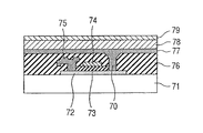
이하, 본 발명의 기본 구성을 제 1 실시예를 나타낸 도 7을 참조하여 설명하겠다.Hereinafter, the basic configuration of the present invention will be described with reference to FIG. 7 showing the first embodiment.
도면에서, 도면부호 70은 드레인 전극, 도면부호 71은 기판, 도면부호 72는 활성층, 도면부호 73은 게이트 절연막, 도면부호 74는 게이트 전극, 도면부호 75는 소스 전극, 도면부호 77은 제2의 전극, 도면부호 78은 발광층, 도면부호 79는 제1의 전극을 나타낸다. 제 1 실시예에서는, 제2의 전극(이후, "하부전극"이라고 함)을 발광층보다 기판에 가깝도록 배치하고, 그 발광층이 유기EL층이고, 제1의 전극 (이후, "대향전극"이라고 함)이 발광층이보다 기판으로부터 더 멀리 배치된다. 상기 구성요소들간의 갭은, 층간절연층(76)으로 채워진다.In the drawing,
우선, 각 구성요소를 상세히 설명한다.First, each component is demonstrated in detail.
(1.기판)(1.substrate)
일반적으로 발광 장치에는 기판의 재료로 유리가 이용되고 있다. 그러나, 본 발명에 사용된 TFT가 저온에서 형성가능하므로, 액티브 매트릭스에서 사용이 곤란한 플라스틱 기판은 본 발명에서 사용가능하다. 이에 따라, 경량인 발광 장치는 거의 손상되지 않고 어느 정도 구부리는 것도 가능하다. 물론, Si 등의 반도체기판과 세라믹 기판도 이용가능하다. 또한, 기판이 평탄하면 금속기판 위에 절연층을 갖는 기판도 이용가능하다.Generally, glass is used as a material of a board | substrate for a light emitting device. However, since the TFT used in the present invention can be formed at a low temperature, a plastic substrate that is difficult to use in an active matrix can be used in the present invention. As a result, the light emitting device can be bent to some extent with little damage. Of course, semiconductor substrates such as Si and ceramic substrates are also available. Also, if the substrate is flat, a substrate having an insulating layer on the metal substrate may be used.
(2.트랜지스터)(2.transistor)
트랜지스터의 활성층은, 원하는 특성 즉, 전자 캐리어 농도가 1×10¹⁸/cm3미만이며, 전자이동도가 1cm2/(Ⅴ·초)이면 어떠한 재료이어도 된다. 그 재료는, 예를 들면 In-Ga-Zn-0계의 비정질 산화물 반도체를 사용한다. 이 비정질 산화물은, 투명막이다. 여기서, 단어, 투과성은, 가시광에 대해 거의 투과적인 경우를 의미할 뿐만 아니라, 가시범위의 광의 적어도 일부분에 대해 광학적으로 투과적인 경우를 포함한다. 광 투과성에 관해, In-Ga-Zn-0계의 비정질 산화물 반도체의 투과율이 50%이상인 것이 바람직하고, 더욱 바람직하게는 80%이상이다. 상기 조성은, Mg를 치환 혹은 첨가하는 것이 가능하다. 발광장치가 In-Ga-Zn-0계의 활성층을 사용한 TFT를 사용하는 경우, 그 TFT가 전압과 전류의 충분한 구동력을 유기EL소자에 공급하므로 유용한 성능을 나타낸다.The active layer of the transistor may be any material as long as the desired characteristics, that is, the electron carrier concentration is less than 1 × 10 18 / cm 3 and the electron mobility is 1 cm 2 / (V · sec). As the material, for example, an In—Ga—Zn-0 based amorphous oxide semiconductor is used. This amorphous oxide is a transparent film. Here, the word, transmissive, means not only a case where the light is substantially transmissive to visible light, but also includes a case which is optically transmissive for at least a portion of the light in the visible range. Regarding the light transmittance, the transmittance of the In—Ga—Zn-0 based amorphous oxide semiconductor is preferably 50% or more, and more preferably 80% or more. The said composition can substitute or add Mg. When the light emitting device uses a TFT using an In—Ga—Zn-0 based active layer, it exhibits useful performance since the TFT supplies sufficient driving force of voltage and current to the organic EL element.
상기 비정질 산화물에 대해서는, 별도로 상세히 설명한다.The amorphous oxide will be described in detail separately.
활성층의 형성에는 상기와 같이 스퍼터링법이나 펄스레이저 증착법이 적합하지만, 생산성에 유리한 각종 스퍼터링법이 보다 바람직하다. 또한, 이 활성층과 기판 사이에는 적당하게 버퍼층을 삽입하는 것도 효과적이다.Although sputtering method and pulse laser deposition method are suitable for formation of an active layer as mentioned above, various sputtering methods which are favorable for productivity are more preferable. It is also effective to insert a buffer layer appropriately between the active layer and the substrate.
게이트 절연막에는 전술한 A1203, Y20, 및 HfO2의 임의의 하나, 또는 그것들의 화합물을 적어도 2개 이상 포함한 혼정 화합물이 바람직하지만, 또 다른 화합물이어도 된다.The gate insulating film is preferably a mixed crystal compound containing any one of A1 2 O 3 , Y 2 O, and HfO 2 described above, or at least two or more compounds thereof, but may be another compound.
사용가능한 소스 전극과 드레인 전극은 ITO로 대표되는 도전성 산화물과, Au 등의 금속을 포함한다. 그러나, 상기 전극은, 활성층과 오믹 또는 거의 오믹으로 접속되는 것이 바람직하다. 또한, 그 드레인 전극은, 제2 전극을 바이패스하지 않고 발광층과 직접 접속되어도 된다.Usable source and drain electrodes include conductive oxides represented by ITO and metals such as Au. However, it is preferable that the electrode is connected to the active layer ohmic or almost ohmic. In addition, the drain electrode may be directly connected to the light emitting layer without bypassing the second electrode.
(3.발광층)(3.light emitting layer)
발광층은 TFT에서 구동할 수 있는 것이면 한정되지 않지만, 유기EL이 특히 바람직하다. 본 발명에 사용하는 유기EL층(78)은 단층일 경우는 적지만, 일반적으로, 이하에 나타낸 것처럼, 복수층으로 이루어진 구성에서 사용된다. 이하에서, "전자수송층"은 전자수송 기능을 갖는 발광층을 의미한다.The light emitting layer is not limited as long as it can drive in the TFT, but organic EL is particularly preferable. The
홀 수송층/발광층+전자수송층Hall transport layer / light emitting layer + electron transport layer
홀 수송층/발광층/전자수송층Hall transport layer / light emitting layer / electron transport layer
홀 주입층/홀 수송층/발광층/전자수송층Hole injection layer / hole transport layer / light emitting layer / electron transport layer
홀 주입층/홀 수송층/발광층/전자수송층/전자주입층Hole injection layer / hole transport layer / light emitting layer / electron transport layer / electron injection layer
전자장벽층과 부착 개선층은 복수의 층 사이에 종종 삽입된다.The electron barrier layer and the adhesion improving layer are often interposed between the plurality of layers.
일반적으로, 발광층의 발광 원리에는 형광과 인광을 사용할 경우가 있지만, 발광 효율로부터 인광을 사용하는 것이 효과적이다. 인광성 재료서는 이리듐 착체가 유용하다. 또한 발광층용 기본 금속에 사용된 폴리머로서는 저분자 폴리머와 고분자 폴리머 양쪽을 이용할 수 있다. 저분자 폴리머를 이용하는 경우, 발광층은 일반적으로 증착법으로 형성되고, 고분자 폴리머를 이용하는 경우 발광층은, 잉크젯법이나 인쇄공정으로 형성가능하다. 예로서는 저분자 폴리머에서는 아민 착물, 안트라센(Anthracene), 희토류 착물, 귀금속 착물, 고분자 폴리머서는 π공역계와 색소 함유 폴리머를 들 수 있다.Generally, although fluorescence and phosphorescence may be used for the light emission principle of a light emitting layer, it is effective to use phosphorescence from light emission efficiency. Iridium complexes are useful for phosphorescent materials. As the polymer used for the base metal for the light emitting layer, both a low molecular polymer and a high polymer can be used. In the case of using a low molecular polymer, the light emitting layer is generally formed by a vapor deposition method, and in the case of using a high molecular polymer, the light emitting layer can be formed by an inkjet method or a printing process. Examples of the low molecular polymer include amine complexes, anthracene, rare earth complexes, precious metal complexes, and π-conjugated systems and pigment-containing polymers.
전자주입층은, 알칼리 금속, 알칼리토류 금속, 그것들의 화합물, 알칼리 금속을 도핑한 유기층으로 이루어진다. 또한, 전자수송층은 알루미늄 착물, 옥사디아졸, 트리아졸 및 페난트롤린으로 이루어진다.The electron injection layer is composed of an organic layer doped with alkali metal, alkaline earth metal, compounds thereof, and alkali metal. The electron transport layer also consists of an aluminum complex, oxadiazole, triazole and phenanthroline.
홀 주입층은, 아릴아민, 프탈로시아닌, 루이스(Lewis) 산으로 도핑된 유기층으로 이루어지고, 홀 수송층은 아릴아민으로 이루어진다.The hole injection layer consists of an organic layer doped with arylamine, phthalocyanine, Lewis acid, and the hole transport layer consists of arylamine.
한편, 도 7은 유기EL소자의 구성 예를 나타내지만, 동일한 구성은, 무기EL소자에도 사용될 수 있다.7 shows an example of the configuration of the organic EL element, the same structure can be used for the inorganic EL element.
(4.제1의 전극)(4.1st electrode)
제1의 전극이, 대향전극인 경우에 대해 설명한다. 톱 에미션 타입 또는 보텀 에미션타입에서 사용되는지에 따라 또한 음극이나 양극인가에 따라 그 대향전극의 바람직한 재료가 다르다.The case where the 1st electrode is a counter electrode is demonstrated. The preferred material of the counter electrode differs depending on whether it is used in the top emission type or the bottom emission type and whether the cathode or the anode is applied.
대향전극이 톱 에미션 타입에서 사용되면, 투명성이 필요하고, 대향전극이 양극으로서 사용되는 경우, 모두 상기 투명도전성 산화물인 ITO, 도전성 산화 주석, 도전성 ZnO, In-Zn-0, 전자 캐리어 농도가 1×10¹⁸/cm3이상의 In-Ga-Zn-0계도 이용가능한 재료이다. 대향전극이 음극일 경우에는, 알칼리 금속이나 알칼리토류금속을 도프한 합금을 수십 nm이하로 형성하고, 그 상부에 투명 도전성 산화물을 형성함에 의해 대향전극을 형성할 수 있다.When the counter electrode is used in the top emission type, transparency is required, and when the counter electrode is used as the anode, all of the transparent conductive oxides ITO, conductive tin oxide, conductive ZnO, In-Zn-0, and electron carrier concentrations In-Ga-Zn-0 systems of 1 × 10 18 / cm 3 or more are also available materials. When the counter electrode is a cathode, the counter electrode can be formed by forming an alloy doped with alkali metal or alkaline earth metal to several tens of nm or less, and forming a transparent conductive oxide thereon.
대향전극이 보텀 에미션 타입일 경우에는, 투명할 필요가 없으므로, 그것이 양극일 경우에는 Au합금이나 Pt합금이 이용가능하고, 음극일 경우에는 Ag첨가 Mg, Li첨가 Al, 실리사이드, 보라이드(Boride), 질화물이 이용가능하다.If the counter electrode is of the bottom emission type, it is not necessary to be transparent, so if it is an anode Au alloy or Pt alloy is available, and if it is a cathode, Ag addition Mg, Li addition Al, silicide, boride (Boride) Nitrides are available.
(5.제2의 전극)(Second electrode)
제2의 전극은 드레인 전극에 접속된다. 제2의 전극은, 드레인 전극의 조성과 같은 조성이거나 다른 조성이어도 된다.The second electrode is connected to the drain electrode. The second electrode may be the same composition as the composition of the drain electrode or may have a different composition.
제2의 전극은, 하부전극이어도 된다. 그 하부전극은, 기판 또는 발광층을 따라 층 구성으로 형성되어도 된다.The second electrode may be a lower electrode. The lower electrode may be formed in a layer structure along the substrate or the light emitting layer.
발광층이 유기EL소자로 대표되는 전류주입형인 경우에는, 그 구성에 의해 바람직한 하부전극이 있다.In the case where the light emitting layer is a current injection type represented by an organic EL element, there is a preferable lower electrode by its configuration.
하부전극에 접속되는 발광층이 음극일 경우에는, 그 하부전극은 일함수가 작은 금속이 바람직하다. 그 하부전극은, 이를테면 Ag첨가 Mg, Li첨가 Al, 실리사이드, 보라이드, 질화물로 이루어진다. 이 경우에, 그것과 직접 연결되는 것보다 배선을 통한 TFT의 드레인 부분과 접속되는 것이 더욱 바람직하다.When the light emitting layer connected to the lower electrode is a cathode, the lower electrode is preferably a metal having a small work function. The lower electrode is made of, for example, Ag-added Mg, Li-added Al, silicide, boride, or nitride. In this case, it is more preferable to be connected with the drain portion of the TFT through wiring than directly connected thereto.
하부전극에 접속되는 발광층이 양극일 경우에는, 그 하부전극은 일함수가 큰 금속이 바람직하다. 그 하부전극은, 이를테면 ITO, 도전성 산화 주석, 도전성 ZnO, In-Zn-O, Pt합금 및 금합금으로 이루어진다. 또한, 전자 캐리어 농도가 1×10¹⁸/cm3이상의 In-Ga-Zn-0계도 이용가능하다. 이 경우에는, TFT에 사용된 경우와 다른 하부전극이 산화물인 것이 더욱 바람직하다. 이를테면, 전자 캐리어 농도가 1×10¹⁹/cm3이상이 바람직하다. 하부전극을 ITO나 In-Ga-Zn-0계 산화물(고캐리어 농도)로 제조된 경우에는, 투명하기 때문에, 하부전극은, 보텀 에미션 타입에서 사용되는 경우에도 고 개구 면적비를 제공할 수 있다. 그 하부전극이 드레인 전극과 직접 접속하는 경우에, 특히 ITO, 상기 In-Ga-Zn-0계 산화물(고캐리어 농도), Au합금이 특히 바람직하다.When the light emitting layer connected to the lower electrode is an anode, the lower electrode is preferably a metal having a large work function. The lower electrode is made of, for example, ITO, conductive tin oxide, conductive ZnO, In-Zn-O, Pt alloy and gold alloy. In addition, an In-Ga-Zn-0 system having an electron carrier concentration of 1 × 10 18 / cm 3 or more can also be used. In this case, it is more preferable that the lower electrode different from the case used for the TFT is an oxide. For example, the electron carrier concentration is preferably at least 1 × 10 19 / cm 3 . When the lower electrode is made of ITO or In-Ga-Zn-0-based oxide (high carrier concentration), since the lower electrode is transparent, the lower electrode can provide a high aperture area ratio even when used in a bottom emission type. . In particular, when the lower electrode is directly connected to the drain electrode, ITO, the In-Ga-Zn-0-based oxide (high carrier concentration) and Au alloy are particularly preferable.
전술한 드레인 전극을 하부전극에 직접 접속할 경우에, 하부전극은 홀 주입형인 것이 바람직하다. 특히 하부전극으로서 ITO, Al이나 Ga가 도프된 ZnO, 캐리어 농도가 1×10¹⁸/cm3이상의 In-Ga-Zn-0계 산화물의 재료가 바람직하다. 특히 In-Ga-Zn-0계 산화물이 전극 및 활성층으로서 사용되는 경우, 활성층In-Ga-Zn-0의 일부의 캐리어 농도를 산소 결함을 도입하는 방법등에 의해 증가될 수 있고, 발광장치는 간단하고 효과적으로 구성된다. 이 경우에는, 한눈에, 활성층 위에 홀 수송층과 홀 주입층이 형성되어 있다. 이 구성은 본 발명의 범위내이어야 한다. 구체적으로, 그것은, 하부전극과 드레인 전극이 활성층의 일부로 일체가 된 구성을 의미한다.In the case where the above-mentioned drain electrode is directly connected to the lower electrode, the lower electrode is preferably of a hole injection type. In particular, a material of ITO, Al or Ga-doped ZnO, and an In—Ga—Zn-0-based oxide having a carrier concentration of 1 × 10 18 / cm 3 or more is preferable as the lower electrode. In particular, when In-Ga-Zn-0-based oxides are used as electrodes and active layers, the carrier concentration of a part of the active layer In-Ga-Zn-0 can be increased by a method of introducing oxygen defects, and the light emitting device is simple. And effectively configured. In this case, at a glance, a hole transport layer and a hole injection layer are formed on the active layer. This configuration should be within the scope of the present invention. Specifically, it means a configuration in which the lower electrode and the drain electrode are integrated as part of the active layer.
(6.층간절연층)(6.Interlayer Insulation Layer)
특히, 제2의 전극이 하부전극일 경우, 하부전극(77)의 하지층인 층간절연층(76)은, 게이트 절연막의 재료와 같은 재료를 사용하는 것이 가능하다. 물론, 평탄층을 얻기 위해서 다른 재료의 절연층도 형성가능하다. 예를 들면, 폴리이미드막을 스핀코트할 수 있고, 산화 실리콘을 플라즈마 CVD법, PECVD법, LPCVD법, 혹은 실리콘알콕시드의 도포 및 소성으로도 형성가능하다. 층간절연층에는 소스전극이나 드레인 전극을 접속하기 위한 콘택홀을 형성하는 것이 적당히 필요하게 된다.In particular, when the second electrode is a lower electrode, the
(7.전극선 및 기타)(7.electrode wire and others)
게이트 전극선인 주사 전극선과 신호 전극선 등의 전극선으로서는, Al이나 Cr, W등의 금속이나, WSi등의 실리사이드 등이 이용가능하다.As electrode lines such as scan electrode lines and signal electrode lines that are gate electrode lines, metals such as Al, Cr, and W, silicides such as WSi, and the like can be used.
다음에, 각 구성요소간의 관계를 상세히 설명한다.Next, the relationship between each component is demonstrated in detail.
먼저, 제 1 실시예는, 도 7을 참조하여 설명하고, 여기서 하부전극은 배선으로 드레인 전극과 일부 접속된다.First, the first embodiment will be described with reference to FIG. 7, wherein the lower electrode is partially connected to the drain electrode by wiring.
(제 1 실시예)(First embodiment)
소스전극(75)과 드레인 전극(70)은, 활성층(72)과 직접 접속되고, 그 활성층(72)을 통과하는 전류는, 게이트 절연막(73)을 통해 게이트 전극(74)에 의해 제 어된다.The
발광층인 유기EL층(78)은, 하부전극(77) 및 콘택홀의 배선을 거쳐서 드레인 전극(70)과 접속되어 있다. 하부전극(77)과 TFT부분의 사이에는 층간절연층(76)이 있고, 전기적으로 절연되어 있다. 이 층간절연층(76)은 단층일 필요는 없고, 오히려 일반적으로는 게이트 절연막이나 게이트 전극 상부에 설치하는 절연층, 그리고 평탄화하기 위한 일반적인 층간절연층으로 이루어진다.The
유기EL층(78)의 상부에는 대향전극(79)이 있고, TFT가 ON상태일 때에는 유기EL층(78)에는 전압이 인가되어서 발광에 이른다.On the upper side of the
또한, 드레인 전극(70)은, 상기 제2의 전극과 전기적으로 접속되거나, 제2의 전극 자체이다.The
도 7에서는, TFT의 윗면에도 유기EL층(78)이 존재하는 고개구 면적비의 예를 나타냈지만, 응용상 문제가 생기지 않는 한, TFT부분 이외의 부분에 형성되어도 된다. 그러나, 유기EL층(78)을 도 7에 도시된 구성에서 사용하는 경우, 유기EL층(78)의 하부는 가능한 평탄한 것이 바람직하다.In FIG. 7, an example of a high opening area ratio in which the
도 7에서는, 드레인 전극(70)을 하부전극(77)에 접속하고 있지만, 사용방법에 따라서는, 소스 전극(75)을 하부전극(77)에 접속한다. 즉, 본 발명에서는, 비정질 산화물을 포함한 트랜지스터의 소스 전극과 드레인 전극 중 한쪽을, 발광층을 삽입하는 전극에 접속하는 것이 특징이다. 또한, 발광층(78)의 하부전극(77)이 애노드일 경우에는, 해당 애노드측에, TFT의 소스 전극을 접속하는 구성도 바람직하다.In FIG. 7, the
(발광 장치의 제작에 대해서)(About production of light-emitting device)
여기서는, 드레인 전극과 하부전극을 배선을 거쳐서 접속하고, 유기EL을 발광소자로서 사용한 구성의 예를 참조하여, 본 발명에 따른 발광장치 제조방법을 설명한다.Here, the method of manufacturing the light emitting device according to the present invention will be described with reference to an example of a configuration in which the drain electrode and the lower electrode are connected via wirings and the organic EL is used as the light emitting element.
(트랜지스터 제작)(Transistor production)
트랜지스터는,Transistors,
전자 캐리어 농도가 1×10¹⁸/cm3가 되도록 후술하는 조건에서, 펄스레이저 증착법에 의해, 유리 기판 위에 In-Ga-Zn-0계 비정질 산화물 반도체의 박막을 120nm 퇴적시키고, InGaO3(ZnO)4조성을 갖는 다결정 소결체를 타겟으로서 사용하는 스텝과,A 120 nm thin film of an In—Ga—Zn-0 based amorphous oxide semiconductor was deposited on a glass substrate by a pulsed laser deposition method under the conditions described below so that the electron carrier concentration was 1 × 10 18 / cm 3 , and InGaO 3 (ZnO) Using a polycrystalline sintered body having four compositions as a target,
그 위에, 쳄버내 산소분압을 1Pa미만으로 제어해서, 펄스레이저 퇴적법에 의해 전기전도도가 높은 InGaO3(ZnO)4을 30nm 더 적층하고, 그 위에 소스전극 및 드레인 전극으로서 Au의 막을 전자빔증착법에 의해 50nm 형성하는 스텝과,On top of that, the oxygen partial pressure in the chamber is controlled to be less than 1 Pa, and InGaO 3 (ZnO) 4 having high electrical conductivity is further laminated by pulse laser deposition, and an Au film as a source electrode and a drain electrode is deposited on the electron beam deposition method. Forming 50nm by
게이트 절연막으로서 Y203을, 게이트 전극으로서 Au를 전자빔증착법에 의해 각각 90nm 및 5Onm로 더 성막하는 스텝에 의해, 제작한다. 상기 일련의 프로세스에 있어서 포트리소그래피법과 리프트 오프법에 의해 각각의 층을 원하는 사이즈로 형성한다. 더욱이, 절연층을 같은 방법으로 성막한다. 그후, 드레인 전극용의 컨택트홀을 형성해 둔다.A step of further forming Y 2 O 3 as a gate insulating film and Au as a gate electrode at 90 nm and 5 Onm, respectively, by an electron beam deposition method is performed. In the series of processes, each layer is formed to a desired size by the port lithography method and the lift off method. Further, an insulating layer is formed in the same manner. Thereafter, contact holes for drain electrodes are formed.
(하부전극층 제작)(Bottom electrode layer production)
그 후, ITO의 막을 스퍼터링법에 의해 300nm 형성해서 하부전극을 형성한 후, 드레인 전극과 하부전극을 컨택트홀에 형성된 배선을 거쳐서 접속한다.Thereafter, a 300 nm film of ITO is formed by the sputtering method to form a lower electrode, and then the drain electrode and the lower electrode are connected via a wiring formed in the contact hole.
(유기EL발광층 제작)(Organic EL light emitting layer production)
다음 스텝에서는, 저항증발법에 의해 4, 4'-비스[N, N-디아미노]-4"-페닐-트리페닐 아민을 홀 주입층으로서 60nm 형성하고, 그 위에 홀 수송층으로서 4, 4'-비스[N-(1-나프틸)-N-페닐아미노]비페닐 막을 20nm 형성하고, 발광층으로서 4, 4'-비스(2, 2-디페닐) 비닐 막을 40nm 형성하고, 전자수송층으로서 트리스(tris)(8-퀴노리놀)알루미늄 막을 20nm 형성하여서, 유기EL발광층을 제작한다.In the next step, 60 nm of 4, 4'-bis [N, N-diamino] -4 "-phenyl- triphenyl amine is formed as a hole injection layer by the resistance evaporation method, and 4, 4 'is formed on it as a hole transport layer. 20 nm of a bis [N- (1-naphthyl) -N-phenylamino] biphenyl film was formed, a 40
(대향전극의 제작)(Manufacture of counter electrode)
최후에, 2중 증착법에 의해 Al과 Ag의 합금의 막을 50nm, Al의 막을 50nm로 형성하여서 대향전극을 제작한다.Finally, a counter electrode is produced by forming a film of an alloy of Al and Ag by 50 nm and a film of Al by 50 nm by a double deposition method.
상기한 소자에 프로브를 접촉하여서 구동하면, 기판 뒤편에서, 즉 상기 소자의 보텀 에미션 타입에서 청색의 발광을 얻을 수 있다.When the probe is brought into contact with the above-described device, blue light emission can be obtained behind the substrate, that is, at the bottom emission type of the device.
또한, In-Ga-Zn-O계 비정질 산화물 반도체가 산소결손량을 제어해서 원하는 전자 캐리어 농도를 획득하는 것이 본 실시예에 있어서는 중요하다.In addition, it is important in this embodiment that the In—Ga—Zn—O based amorphous oxide semiconductor controls the amount of oxygen deficiency to obtain a desired electron carrier concentration.
상기 기재에 있어서는, 투명 산화물막의 산소량(산소결손량)의 제어를, 성막시에 산소를 소정 농도 포함한 분위기에서 행함으로써 제어하고 있지만, 이전의 스텝에서 형성된 해당 산화물 막을 산소를 포함한 분위기에서 후처리해서 산소결손량을 제어(감소 또는 증가)하는 것도 바람직한 것이다.In the above description, the oxygen amount (oxygen deficiency amount) of the transparent oxide film is controlled by performing oxygen in a predetermined concentration at the time of film formation, but the oxide film formed in the previous step is post-processed in an atmosphere containing oxygen. It is also desirable to control (reduce or increase) the amount of oxygen deficiency.
효과적으로 산소결손량을 제어하기 위해서는, 산소를 포함한 분위기의 온도 를 0℃이상 300℃이하, 바람직하게는, 25℃이상, 250℃이하, 더 바람직하게는 100℃이상 200℃이하로 행하는 것이 좋다.In order to effectively control the amount of oxygen deficiency, the temperature of the atmosphere containing oxygen is preferably 0 ° C or more and 300 ° C or less, preferably 25 ° C or more and 250 ° C or less, more preferably 100 ° C or more and 200 ° C or less.
물론, 성막시에도 산소를 포함한 분위기에서 행하고, 또한 산소를 포함한 분위기에서 후처리해도 된다. 또한, 상기 방법이 소정의 전자 캐리어 농도(1×10¹⁸/cm3미만)를 제공하면, 성막시에는, 산소분압 제어는 행하지 않고, 성막 후의 후처리를 산소를 포함한 분위기중에서 행해도 된다.As a matter of course, the film formation may be carried out in an atmosphere containing oxygen, or may be post-treated in an atmosphere containing oxygen. In addition, if the above method provides a predetermined electron carrier concentration (less than 1 × 10 18 / cm 3 ), the oxygen partial pressure control may not be performed at the time of film formation, and the post-treatment after film formation may be performed in an atmosphere containing oxygen.
또한, 본 발명에 있어서의 전자 캐리어 농도의 하한치는, 얻어진 산화물막을 어떤 소자, 회로 혹은 장치에 사용하는지에도 의존하지만, 예를 들면 1×10¹⁴/cm3이상이다.In addition, although the lower limit of the electron carrier density | concentration in this invention depends on what kind of element, circuit, or apparatus which the obtained oxide film uses, it is 1 * 10 <14> / cm <3> or more, for example.
다음에는, 도 9를 참조하여, 하부전극을 사이에 배선을 개재하지 않고서 드레인 전극과 직접 접속한 제 2 실시예를 설명하겠다.Next, referring to Fig. 9, a second embodiment in which the lower electrode is directly connected to the drain electrode without interposing the wiring will be described.
(제2의 실시예)(2nd Example)
도 9에서, 도면부호 91은 기판, 도면부호 92는 본 발명 특유의 반도체 재료로 이루어진 활성층, 도면부호 93은 게이트 절연막, 도면부호 94는 게이트 전극, 도면부호 95는 소스 전극, 도면부호 96은 절연층, 도면부호 97은 하부전극이다. 또한, 이 하부전극(97)은, 드레인 전극 위에 적층되어 있거나, 드레인 전극과 동일하다, 즉 드레인 전극 자체이다. 또한, 도면부호 98은 유기EL층, 도면부호 99는 대향전극이다.In Fig. 9,
본 실시예는, 기본적으로는, 배선을 통해 드레인전극과 하부전극의 일부가 접촉하는 제1의 실시예의 구성과 동일한 형태이지만, 드레인 전극과 발광층이, 기판(91)의 위치에서 보았을 경우에, 동일한 중복 영역에 적층 되어 있고, 그 사이에 하부전극이 있는 서로 다른 구성을 갖는다.This embodiment is basically the same as the configuration of the first embodiment in which a part of the drain electrode and the lower electrode are in contact with each other via wiring, but when the drain electrode and the light emitting layer are viewed from the position of the
드레인 전극과 하부전극은, 동일한 부재이어도 된다. 이 경우에, 드레인 전극은 전자 혹은 홀을 유기EL층에 효과적으로 주입하는 능력을 가질 필요가 있다.The drain electrode and the lower electrode may be the same member. In this case, the drain electrode needs to have the ability to effectively inject electrons or holes into the organic EL layer.
활성층의 드레인 전극하부에 대응한 일부에서의 전자 캐리어 밀도를 산소결함을 늘림으로써 1×10¹⁸/cm3이상으로 제어하는 것이 바람직하다. 그리고, 드레인 전극과 하부전극을 겸비하는 것이 가능하다. 이 경우에, 활성층은 In-Ga-Zn-0막으로 이루어지고, 홀 주입층으로서 기능하고, 발광층의 양극부분과 접속되는 것이 바람직하다.It is preferable to control the electron carrier density at a portion corresponding to the drain electrode lower portion of the active layer to 1 × 10 18 / cm 3 or more by increasing the oxygen defect. And it is possible to have a drain electrode and a lower electrode. In this case, it is preferable that the active layer is made of an In—Ga—Zn-0 film, and functions as a hole injection layer, and is connected to the anode portion of the light emitting layer.
도 9에서는 TFT층 상부에 발광층을 사용한 예를 게시하고 있지만, 기능상 문제를 발생하지 않으면, 제 1전극인 대향전극과 제 2 전극인 하부전극이 반대로 되고, 제1 전극이 드레인 전극 위에 직접 적층되는 구성도 허용 가능하다. 이 경우, 하부전극인 제2 전극은, 겉으로 보기에는 상부에 있지만, 기능상 드레인 전극과 접속되어 있으면 같은 것이다. 특히, 무기EL층을 이용하는 경우, 프로세스 내성이 유기EL층과 비교해서 강하므로, 반대의 경우도 있을 수 있다.In FIG. 9, an example in which a light emitting layer is used on the TFT layer is disclosed. However, if a functional problem does not occur, the counter electrode as the first electrode and the lower electrode as the second electrode are reversed, and the first electrode is directly stacked on the drain electrode. Configuration is also acceptable. In this case, although the 2nd electrode which is a lower electrode is seemingly upper part, if it is functionally connected with the drain electrode, it is the same. In particular, in the case of using the inorganic EL layer, since the process resistance is stronger than that of the organic EL layer, there may be a reverse case.
본 발명에 따른 발광장치의 바람직한 구성에서, 제1 및 제2 전극은, 대향전극 및 하부전극이고, 전계 효과형 트랜지스터는 TFT이고, TFT의 활성층은 In, Ga 및 Zn을 포함하고, 그 활성층의 적어도 일부분은 비정질 산화물이고, 발광층의 일부분은 TFT의 드레인 전극과 전기적으로 접속된다.In a preferred configuration of the light emitting device according to the present invention, the first and second electrodes are the counter electrode and the lower electrode, the field effect transistor is a TFT, and the active layer of the TFT includes In, Ga, and Zn, and the active layer of At least a part is an amorphous oxide, and a part of the light emitting layer is electrically connected with the drain electrode of the TFT.
본 발명에 따른 발광장치에서, 발광층의 일부분은 직접 드레인전극에 접속되거나, 발광층의 일부분은 배선을 통해 드레인전극과 접속되어도 된다. 상기와 같이 접속된 발광층의 일부분은, 발광층의 양극측 또는 음극측인 것이 바람직하다.In the light emitting device according to the present invention, a part of the light emitting layer may be directly connected to the drain electrode, or a part of the light emitting layer may be connected to the drain electrode through wiring. It is preferable that a part of the light emitting layer connected as mentioned above is an anode side or a cathode side of a light emitting layer.
드레인전극과 상기 하부전극의 적어도 한쪽은 투명성과 전기도전성 산화물이다.At least one of the drain electrode and the lower electrode is transparent and electroconductive oxide.
다음에, 디스플레이 응용의 구성 예인 제3 실시예를 도 8을 참조하여 설명한다.Next, a third embodiment which is a configuration example of a display application will be described with reference to FIG.
도 9에서는, 드레인 전극(97)을 하부전극으로서도 이용하고 있지만, 발광층의 층구성으 구성에 따라, 소스 전극(95)를 하부전극으로서 이용할 수도 있다. 즉, 본 발명은, 비정질 산화물을 포함한 트랜지스터의 소스 전극과 드레인 전극 중 어느 한쪽을, 발광층을 삽입하는 전극에 접속 등을 하는 것을 특징으로 한다.In FIG. 9, the
(제3의 실시예)(Third Embodiment)
도 8에서, 도면부호 81은 유기EL층(84)을 구동하기 위한 트랜지스터이며, 유기EL층(84)과 이 유기EL층(84)을 끼운 한 쌍의 전극을 갖는 발광소자에 전류를 흘려보낸다. 도면부호 82는 화소를 선택하는 트랜지스터(2)이며, 발광소자에 흘려보내는 전류를 결정하는 화상신호를 트랜지스터(81)의 게이트에 공급한다.In Fig. 8,
또한, 콘덴서(83)는, 선택된 상태를 유지하도록 설치되어, 공통 전 극 선(87)과 트랜지스터 2의 소스전극 부분과의 사이에 전하를 축적하고, 트랜지스터 1의 게이트의 신호를 유지하고 있다. 화소선택은 주사 전극선(85)과 신호 전극선(86)에 의해 결정된다.In addition, the
이하, 그 구성을 더 구체적으로 설명한다.Hereinafter, the configuration will be described in more detail.
행선택신호가 드라이버 회로(도면에 나타내지 않는다)에 주사 전극(85)을 통해서 게이트 전극에 펄스신호로 인가됨과 동시에, 별도의 드라이버 회로(도면에 나타내지 않는다)에 신호 전극(86)을 통해서 화상신호가 트랜지스터(82)에 인가되어서 화소가 선택된다.The row selection signal is applied to the driver circuit (not shown) as a pulse signal to the gate electrode through the
이 때, 트랜지스터 82가 ON이 되어 신호 전극선(86)과 트랜지스터 82의 소스전극의 사이에 있는 콘덴서(83)에 전하가 축적된다. 이에 따라, 트랜지스터 81의 게이트 전압이 화상신호에 대응한 원하는 전압으로 유지되고, 트랜지스터 81은 화상신호에 대응한 전류를 소스전극과 드레인전극간에 흘려보낸다. 이 상태는, 트랜지스터가 다음 신호를 받을 때까지 유지된다. 트랜지스터(81)이 전류를 흘려보내는 동안, 유기EL층(84)에도 전류가 계속 공급되어 발광이 유지되게 된다.At this time, the
이 도 8의 예에서는, 1화소에 2개의 트랜지스터, 1개의 콘덴서를 사용한 구성이지만, 이 구성은 성능을 향상시키기 위해서 더욱 많은 트랜지스터를 구비하여도 된다.In the example of FIG. 8, two transistors and one capacitor are used for one pixel, but this configuration may include more transistors to improve performance.
본질적인 것은, 트랜지스터 부분에 본 발명의 저온에서 형성할 수 있어 투명한 In-Ga-Zn-0계 산화물로 예시되는 비정질산화물의 활성층을 갖는 TFT를 사용함으로써, 노멀리 오프형 TFT를 구현할 수 있어, 불필요한 발광이 억제된 발광 장치를 제공할 수 있다는 것이다. 또한, 상기 TFT는 고콘트라스트의 전자사진장치와 표시장치를 제공할 수도 있다.Essentially, by using a TFT having an active layer of amorphous oxide, which can be formed at a low temperature of the present invention and exemplified by a transparent In—Ga—Zn-0-based oxide, a normally off TFT can be realized, which is unnecessary. It is possible to provide a light emitting device in which light emission is suppressed. The TFT may also provide a high contrast electrophotographic device and a display device.
(제4의 실시예)(4th Example)
본 발명의 제4의 실시예는, 도 11과 도 12에 나타나 있는 바와 같이 보텀 에미션형의 발광 장치이다.A fourth embodiment of the present invention is a bottom emission type light emitting device as shown in Figs.
즉, 발광장치는, 광 투과성의 기판 위에, 상기 발광층 및, 상기 전계 효과형 트랜지스터가 설치되어 있고, 상기 발광층으로부터 출력되는 빛이, 상기 기판을 거쳐서 출력된다. 도 11에서는, 발광소자(2160)의 바로 아래에도, 비정질 산화물로 형성되는 활성층(채널층 2101)이 설치되지만, 그 바로 아래에 없어도 된다. 물론, 도 11의 구성의 경우에는, 발광층 2108로부터의 빛이, 상기 비정질산화물로 구성되어 있는 활성층과 기판(2100)을 투과하게 된다.That is, in the light emitting device, the light emitting layer and the field effect transistor are provided on a light transmissive substrate, and light output from the light emitting layer is output through the substrate. In FIG. 11, an active layer (channel layer 2101) made of amorphous oxide is provided immediately below the
그런데, 본 발명에 따른 발광 장치를 일차원으로 배열한 광원을 제작할 수 있고, 도 13에 나타나 있는 바와 같이 감광체의 광전도체 드럼(2350)과 조합시켜서 장치를 제작할 수 있다. 즉, 감광체(2350)와, 감광체를 대전시키기 위한 대전기(도면에 나타내지 않는다)와, 감광체에 잠상을 형성하기 위해서 감광체를 노광하기 위한 노광 광원(2300)과, 상기 잠상을 현상하기 위한 현상기(도면에 나타내지 않는다)를 갖는 전자사진장치를 구성할 수 있다.By the way, the light source which arrange | positioned the light emitting device which concerns on this invention in one dimension can be manufactured, and a device can be manufactured by combining with the
이하에, 상기 제1 및 제2의 실시예에 있어서 설명한 비정질 산화물에 대해서, 상세히 설명한다.The amorphous oxide described in the first and second embodiments will be described in detail below.
(비정질 산화물)(Amorphous Oxide)
이하, 본 발명의 상기 실시예 1-3에서 이용한 활성층을 설명한다.Hereinafter, the active layer used in Examples 1-3 of the present invention will be described.
본 발명의 비정질산화물의 전자 캐리어 농도는, 실온에서 측정된 값이다. 실온이란, 예를 들면 25℃이며, 구체적으로는 0℃부터 40℃정도의 범위에서 적당하게 선택되는 온도다. 또한, 본 발명에 따른 비정질 산화물의 전자 캐리어 농도는, 0℃로부터 40℃의 범위 모두에 있어서, 1018/cm3미만을 충족할 필요가 없다. 예를 들면, 25℃에 있어서, 전자 캐리어 농도 1018/cm3미만이 허용가능하다. 또한, 전자 캐리어 농도를 더욱 인하, 1×10¹⁷/cm3이하, 더욱 바람직하게는 1×10¹⁶/cm3이하로 하면, 노멀리 오프상태의 TFT가 높은 생산력으로 제조될 수 있다.The electron carrier concentration of the amorphous oxide of the present invention is a value measured at room temperature. Room temperature is 25 degreeC, for example, It is the temperature suitably selected in the range of about 0 degreeC-about 40 degreeC specifically ,. In addition, the electron carrier concentration of the amorphous oxide according to the present invention does not have to satisfy less than 10 18 / cm 3 in all of the range from 0 ° C to 40 ° C. For example, at 25 ° C., an electron carrier concentration of less than 10 18 / cm 3 is acceptable. Further, when the electron carrier concentration is further lowered to 1 × 10 17 / cm 3 or less, more preferably 1 × 10 16 / cm 3 or less, the TFT in the normally off state can be manufactured with high productivity.
본 명세서에서, "1018/cm3미만"은, "바람직하게는 1×10¹⁸/cm3미만 및 더욱 바람직하게는 1.0×10¹⁸/cm3미만"을 의미한다. 전자 캐리어 농도의 측정은, 홀 효과측정에 의해 구할 수 있다.As used herein, "less than 10 18 / cm 3 " means "preferably less than 1x10 18 / cm 3 and more preferably less than 1.0x10 18 / cm 3 ". The measurement of the electron carrier concentration can be obtained by Hall effect measurement.
또한, 본 발명에 있어서, 비정질 산화물은, X선 회절 스펙트럼에 있어서, 할로(halo) 패턴이 관측되고, 특정한 회절선을 나타내지 않는 산화물이다.In the present invention, the amorphous oxide is an oxide in which a halo pattern is observed in the X-ray diffraction spectrum and does not exhibit a specific diffraction line.
본 발명의 비정질 산화물에 있어서의, 전자 캐리어 농도의 하한값은, TFT의 채널층으로서 적용할 수 있으면 한정되는 것은 아니고, 그 하한값은, 예를 들면, 1×10¹²/cm3이다.The lower limit of the electron carrier concentration in the amorphous oxide of the present invention is not limited as long as it can be applied as the channel layer of the TFT, and the lower limit thereof is, for example, 1 × 10 12 / cm 3 .
따라서, 본 발명에 있어서는, 후술하는 예와 같이 비정질 산화물의 재료, 조 성비, 제조 조건등을 제어하여, 예를 들면 전자 캐리어 농도를, 1×10¹²/cm3부터 1×10¹⁸/cm3까지, 바람직하게는 1×10¹³/cm3부터 1×10¹⁷/cm3까지, 더욱 바람직하게는 1×10¹⁵/cm3부터 1×10¹⁶/cm3까지의 범위로 조정한다. 상기 비정질 산화물로서는, InZnGa산화물의 이외에도, In산화물, InxZn1-x산화물(0.2≤x≤1), InxSn1-x산화물(0.8≤x≤1), Inx(Zn, Sn)1-x산화물(0.15≤x≤1)로부터 적당하게 선택할 수 있다. 또한, Inx(Zn, Sn)1-x산화물은, Inx(ZnySn1-y)1-x로 기재될 수 있다(0≤y≤1)이다.Therefore, in the present invention, the material, composition ratio, manufacturing conditions, and the like of the amorphous oxide are controlled as in the examples described below, and the electron carrier concentration is controlled from 1 × 10 12 / cm 3 to 1 × 10 18 / cm 3, for example. To 1 × 10 13 / cm 3 to 1 × 10 17 / cm 3 , more preferably 1 × 10 15 / cm 3 to 1 × 10 16 / cm 3 . As the amorphous oxide, in addition to InZnGa oxide, In oxide, In x Zn 1-x oxide (0.2 ≦ x ≦ 1 ), In x Sn 1-x oxide (0.8 ≦ x ≦ 1 ), In x (Zn, Sn) It can select suitably from 1-x oxide (0.15 <= x <= 1 ). Further, the In x (Zn, Sn) 1-x oxide may be described as In x (Zn y Sn 1-y ) 1-x (0 ≦ y ≦ 1).
또한, Zn과 Sn도 포함하지 않는 In 산화물의 경우는, In의 일부를 Ga: InxGa1-x산화물(0≤x≤1)로 치환할 수 있다.In the case of an In oxide not including Zn and Sn, a part of In can be replaced with Ga: In x Ga 1-x oxide (0 ≦ x ≦ 1).
이하에, 본 발명자들이 제작한 전자 캐리어 농도가 1×10¹⁸/cm3의 비정질 산화물에 대해서 상세히 설명한다.Below, the amorphous oxide of the electron carrier density | concentration produced by this inventor of 1 * 10 <18> / cm <3> is explained in full detail.
상기 산화물의 일 그룹은, 결정 상태에 있어서 InGaO3(ZnO)m(m: 6미만의 자연수)로 나타내고, 전자 캐리어 농도가 1×10¹⁸/cm3미만인 In-Ga-Zn-O로 구성된 것을 특징으로 한다.One group of the oxide is represented by InGaO 3 (ZnO) m (m: less than 6 natural number) in the crystal state, and composed of In-Ga-Zn-O having an electron carrier concentration of less than 1x10 18 / cm 3. It features.
상기 산화물의 다른 그룹은, 결정 상태에 있어서 InGaO3(Zn1-xMgxO)m(m: 6미만의 자연수, 0<x≤1)로 나타내고, 전자 캐리어 농도가 1×10¹⁸/cm3미만인 In-Ga-Zn-Mg-O로 구성된 것을 특징으로 한다.Another group of oxides is represented by InGaO 3 (Zn 1-x Mg x O) m (m: less than 6 natural numbers, 0 <x≤1) in the crystal state, and the electron carrier concentration is 1x10 18 / cm It is characterized by consisting of less than 3 In-Ga-Zn-Mg-O.
또한, 이것들의 산화물로 구성되는 막에 있어서, 전자이동도가 1cm2/Ⅴ·sec보다 크도록 설계하는 것도 바람직하다.Moreover, in the film | membrane which consists of these oxides, it is also preferable to design so that electron mobility may be larger than 1 cm <2> / V * sec.
상기 막을 채널층으로서 사용하여, 트랜지스터 오프시의 게이트 전류가 0.1마이크로암페어 미만의 노멀리 오프상태에서, 온-오프비가 1×10³ 초과인 TFT를 제조할 수 있고, 가시광선에 대하여, 투명하고 유연한 TFT가 제조될 수 있다.Using the film as a channel layer, a TFT having an on-off ratio of more than 1 × 10 3 can be manufactured in a normally off state with a gate current of less than 0.1 microamperes when the transistor is off, and is transparent to visible light. Flexible TFTs can be manufactured.
또한, 상기 막은, 전도전자수의 증가와 함께, 전자이동도가 커진다.투명막을 형성하는 기판은, 유리 기판, 플라스틱 기판 또는 플라스틱막으로 이루어진다.The film also has an increased electron mobility with an increase in the number of conductive electrons. The substrate forming the transparent film is made of a glass substrate, a plastic substrate, or a plastic film.
상기 비정질산화물막을 채널층으로서 이용할 때, A1203, Y203, 또는 Hf02로 이루어진 층들 중 적어도 하나, 또는 혼정화합물을, 게이트 절연막으로서 이용할 수 있다.When the amorphous oxide film is used as the channel layer, at least one of the layers consisting of
비정질 산화물에서, 전기 저항을 향상시키기 위한 불순물 이온을 의도적으로 첨가하지 않고, 산소 가스를 포함한 분위기중에서, 성막하는 것도 바람직한 실시예이다.In amorphous oxide, it is also a preferred embodiment to form a film in an atmosphere containing oxygen gas without intentionally adding impurity ions for improving the electrical resistance.
본 발명자들은, 이 반절연성 산화물의 비정질 박막이, 전도전자수의증가와 함께, 전자이동도가 커진다고 하는 특성을 갖고, 그 막을 사용해서 TFT를 작성하고, 온-오프비, 핀치오프 상태에서의 포화 전류, 스위치 속도등의 트랜지스터 특성이 더욱 향상하는 것을 찾아냈다. 또한 비정질 산화물을 이용하여, 노멀리 오프형의 TFT를 제조할 수 있다.The inventors of the present invention have the characteristics that the amorphous thin film of the semi-insulating oxide has a characteristic that the electron mobility increases with the increase of the number of conduction electrons. The TFT is used to form a TFT, and the saturation in the on-off ratio and the pinch-off state is achieved. It has been found that transistor characteristics such as current and switch speed are further improved. In addition, by using amorphous oxide, a normally off type TFT can be manufactured.
비정질 산화물 박막을 막 트랜지스터의 채널층으로서 사용하면, 전자이동도 가 1cm2/V·sec, 바람직하게는 5cm2/Ⅴ·sec 초과로 할 수 있다.When the amorphous oxide thin film is used as the channel layer of the film transistor, the electron mobility can be set to 1 cm 2 / V · sec, preferably 5 cm 2 / V · sec.
전자 캐리어 농도가, 1×10¹⁸/cm3보다 낮고, 바람직하게는, 1×10¹⁶/cm3미만일 때는, 오프시(게이트 전압 무인가시)의 드레인단자와 소스 단자간의 전류를, 10마이크로암페어미만, 바람직하게는 0.1마이크로암페어미만으로 할 수 있다. 또한, 상기 박막을 사용하면, 전자이동도가 1cm2/ Ⅴ·sec 초과, 바람직하게는 5cm2/V·sec 초과시는, 핀치오프 후의 포화 전류를 10마이크로암페어 이상으로 상승시킬 수 있고, 온-오프비를 1×10³보다 높게 상승시킬 수 있다.When the electron carrier concentration is lower than 1 × 10 18 / cm 3 and preferably less than 1 × 10 16 / cm 3 , the current between the drain terminal and the source terminal at the time of off (when no gate voltage is applied) is 10 microamps. It may be less than, preferably less than 0.1 microamps. In addition, using the above thin film, when the electron mobility is more than 1 cm 2 / V · sec, preferably more than 5 cm 2 / V · sec, the saturation current after pinching off can be raised to 10 micro amps or more, and the on- It is possible to raise the off ratio higher than 1 × 10 3 .
TFT에서는, 핀치오프 상태에서는, 게이트 단자에 고전압이 인가되어, 채널 내에는 고밀도의 전자가 존재하고 있다. 그러므로, 본 발명에 의하면, 전자이동도가 증가함에 따라, 포화 전류는 증가될 수 있다. 이에 따라, 온·오프비의 증대, 포화 전류의 증대, 스위칭 속도의 증대 등의, 트랜지스터 특성을 향상시킬 수 있다. 이와 비교하여, 일반적인 화합물중에서는, 전자가 증대하면, 전자간의 충돌에 의해, 전자이동도는 감소한다.In the TFT, in the pinch-off state, a high voltage is applied to the gate terminal, and high-density electrons exist in the channel. Therefore, according to the present invention, as the electron mobility is increased, the saturation current can be increased. Thereby, transistor characteristics, such as an increase in on / off ratio, an increase in saturation current, and an increase in switching speed, can be improved. In contrast, in general compounds, when electrons increase, electron mobility decreases due to collision between electrons.
또한, 상기 TFT의 구조는, 반도체 채널층 위에 게이트 절연체와 게이트 단자를 순차적으로 형성하는 스태거(톱 게이트)이어도 되거나, 게이트 단자 위에 게이트 절연막과 반도체 채널층을 순차적으로 형성하는 역스태거(보텀 게이트)이어도 된다.The TFT may have a stagger (top gate) for sequentially forming a gate insulator and a gate terminal on the semiconductor channel layer, or an inverted stagger (bottom gate) for sequentially forming a gate insulating film and a semiconductor channel layer on the gate terminal. ) May be used.
(제1의 성막처리:PLD법)(1st film formation process: PLD method)
결정 상태에 있어서의 조성이 InGaO3(ZnO)m(m: 6미만의 자연수)의 비정질 산화물 박막은, m의 값이 6미만일 경우에는, 800℃이상의 고온까지, 비정질상태가 안정하게 유지되는 반면에, m의 값이 커짐에 따라, 즉, InGaO3에 대한 ZnO의 비율이 증대하고, ZnO의 조성에 근접함에 따라, 산화물이 결정화하기 쉬워진다. 따라서, 비정질TFT의 채널층으로서는, 산화물의 m의 값이 6미만인 것이 바람직하다.The amorphous oxide thin film whose composition in the crystal state is InGaO 3 (ZnO) m (m: less than 6 natural numbers), when the value of m is less than 6, the amorphous state remains stable up to a high temperature of 800 ° C or higher. As the value of m increases, that is, the ratio of ZnO to InGaO 3 increases, and closer to the composition of ZnO, oxides tend to crystallize. Therefore, as the channel layer of the amorphous TFT, it is preferable that the value of m of the oxide is less than 6.
성막은, InGaO3(ZnO)m조성을 갖는 다결정 소결체를 타겟으로서, 기상 성막법으로 행해지는 것이 바람직하다. 기상성막법 중에서도, 스퍼터링법, 펄스레이저 증착법이 적합하다. 특히, 양산성에 대해서, 스퍼터링법이 적합하다.The film formation, as InGaO 3 (ZnO) target a polycrystalline sintered body having a composition m is preferably performed in a vapor phase growth method. Among the vapor deposition methods, sputtering and pulse laser deposition are suitable. In particular, the sputtering method is suitable for mass productivity.
그러나, 일반적인 조건으로 상기 비정질막을 작성하면, 산소결손이 생겨서, 전자 캐리어 농도를 1×10¹⁸/cm3미만, 전기전도도를 10S/cm이하로 할 수 없다. 이러한 막을 사용했을 경우, 노멀리 오프의 트랜지스터를 구성 할 수 없다.However, when the amorphous film is prepared under general conditions, oxygen deficiency occurs, and the electron carrier concentration cannot be lower than 1 × 10 18 / cm 3 , and the electrical conductivity cannot be lower than 10 S / cm. When such a film is used, a normally off transistor cannot be constituted.
본 발명자들은, 도 14에 도시되는 장치에 의해, 펄스레이저 증착법에서 제작한 In-Ga-Zn-0를 제작했다.The present inventors produced In-Ga-Zn-0 produced by the pulse laser deposition method by the apparatus shown in FIG.
도 14에 나타나 있는 바와 같은 PLD성막 장치를 사용하여, 성막을 행했다.Film formation was performed using the PLD film-forming apparatus as shown in FIG.
도 14에 있어서, 도면부호 701은 RP(로터리 펌프), 702는 TMP(터보 분자펌프), 703은 준비실, 704는 RHEED용 전자총, 705는 기판을 회전시키고, 상하 이동하기 위한 기판 보유 수단, 706은 레이저 입사창문, 707은 기판, 708은 타겟, 709는 라디칼원, 710은 가스 도입구, 711은 타겟을 회전시키고, 상하 이동하기 위한 타겟 보유 수단, 712는 바이패스 라인, 713은 메인 라인, 714는 TMP(터보 분자펌프), 715는 RP(로터리 펌프), 716은 티타늄 게터 펌프, 717은 셔터, 718은 IG(이온 나노미터), 719은 PG(피라니(Pirani) 게이지), 720은 BG(바라트론 게이지), 721은 성장 쳄버이다.In Fig. 14,
KrF엑시머레이저를 사용한 펄스레이저 증착법에 의해, SiO2유리 기판(코닝사제 1737) 위에 In-Ga-Zn-0형 비정질 산화물 반도체 박막을 퇴적시켰다. 퇴적 전의 처리로서, 기판의 초음파에 의한 탈지 세정을, 아세톤, 에탄올, 초순수를 사용하여, 각 5분간 행한 후, 공기중에서 100℃로 건조시켰다.In-Ga-Zn-0 type amorphous oxide semiconductor thin films were deposited on a SiO 2 glass substrate (1737 manufactured by Corning Corporation) by a pulsed laser deposition method using a KrF excimer laser. As a treatment before deposition, degreasing cleaning by ultrasonic waves of the substrate was performed for 5 minutes using acetone, ethanol and ultrapure water, and then dried at 100 ° C in air.
상기 다결정 타겟에는, InGaO3(ZnO)4 소결체 타겟(사이즈: 직경 20mm, 두께 5mm)을 사용했고, 이것은, 출발 원료로서, In2O3,Ga203,ZnO(각 4N시약)을 습식혼합한 후(용매:에탄올), 가소(1000℃,2시간), 건식분쇄, 본소결(1550℃,2시간)을 경과해서 얻을 수 있는 것이다. 그 타겟의 전기전도도는, 90S/cm이었다.As the polycrystalline target, an InGaO 3 (ZnO) 4 sintered compact target (size: 20 mm in diameter, 5 mm in thickness) was used, which was wetted with In 2 O 3 , Ga 2 O 3 , ZnO (each 4N reagent) as a starting material. After mixing (solvent: ethanol), calcining (1000 DEG C, 2 hours), dry grinding and main sintering (1550 DEG C, 2 hours) can be obtained. The electrical conductivity of the target was 90 S / cm.
성장 쳄버의 최종 진공을 2×10⁻⁶Pa로, 성장중의 산소분압을 6.5Pa로 제어해서 성막을 행했다. 성장 쳄버(721)내의 산소분압은 6.5Pa, 기판온도는 25℃이다. 또한, 타겟 708과 막 보유 기판(707) 사이의 거리는, 30mm이며, 입사창문(716)으로부터 입사되는 파워는, 1.5-3mJ/cm2/pulse)의 범위다.또한, 펄스폭은, 20nsec, 반복 주파수는 10Hz, 그리고 조사 스폿 크기는, 1×1mm 스퀘어로 했다. 이러한 상태에서, 성막 속도는 7nm/min로 행했다.The film formation was performed by controlling the final vacuum of the growth chamber to 2 x 10 -6 Pa and the oxygen partial pressure during growth to 6.5 Pa. The oxygen partial pressure in the
상기 얻어진 박막은, 작은 각도 X선 산란법(SAXS)(박막법, 입사각:0.5°)을 행한 바, 명료한 회절 피크는 관측되지 않았다. 그래서, 상기 제작한 In-Ga-Zn-0계 박막을 비정질이라고 판단하였다. X선 반사율과 패턴의 해석으로부터, 평균 자승 거칠기(Rrms)는 약 0.5nm이며, 막두께는 약120nm인 것을 알았다. 형광 X선 스펙트럼(ⅩRF)분석으로부터, 박막의 금속조성비는 In:Ga:Zn=0.98:1.02:4이었다. 전기전도도는, 약1×10⁻²S/cm미만이었다. 전자 캐리어 농도는 약 1×10-16/cm3이하, 전자이동도는 약 5cm2/V·sec라고 추정되었다. 광 흡수 스펙트럼의 해석으로부터, 상기 결과의 비정질 박막의 금제대 에너지 폭은, 약 3eV로 추정되었다.The obtained thin film was subjected to a small angle X-ray scattering method (SAXS) (thin film method, incident angle: 0.5 °), and no clear diffraction peak was observed. Thus, the In-Ga-Zn-0 thin film thus prepared was determined to be amorphous. From the analysis of the X-ray reflectance and the pattern, it was found that the mean square roughness Rrms was about 0.5 nm and the film thickness was about 120 nm. From the fluorescence X-ray spectrum (: RF) analysis, the metal composition ratio of the thin film was In: Ga: Zn = 0.98: 1.02: 4. The electrical conductivity was less than about 1 × 10 −2 S / cm. It was estimated that the electron carrier concentration was about 1 × 10 −16 / cm 3 or less and the electron mobility was about 5 cm 2 / V · sec. From the analysis of the light absorption spectrum, the forbidden band energy width of the resulting amorphous thin film was estimated to be about 3 eV.
이상의 결과에 의해 밝혀진 것은, 상기 제작한 In-Ga-Zn-0계 박막은, 결정의 InGaO3(ZnO)4의 조성에 가까운 비정질 상태를 보이고 있어, 산소결손이 적고, 전기전도도가 작은 투명한 평탄박막이다는 것이다.According to the above results, the In-Ga-Zn-0-based thin film thus produced exhibits an amorphous state close to the composition of InGaO 3 (ZnO) 4 as a crystal, and has a low oxygen deficiency and a low electrical conductivity. It is a thin film.
구체적으로, 도 1을 사용하여 상기 성막을 설명한다. 도 1은, 본 예시와 같은 성막 조건하에서 결정 상태를 가정했을 때의 조성이 InGaO3(ZnO)m(m: 6미만의 정수)인 상기 투명 비정질 산화물 박막의 산소분압에 관한 전자 캐리어 농도의 의존성을 나타낸 것이다.Specifically, the film formation will be described using FIG. 1. Fig. 1 shows the dependence of the electron carrier concentration on the oxygen partial pressure of the transparent amorphous oxide thin film whose composition is assumed to be InGaO 3 (ZnO) m (m: integer less than 6) under the assumption that the crystal state is under the same deposition conditions as in the present example. It is shown.
본 예시와 같은 조건하에서 산소분압을 4.5Pa 초과의 높은 분위기중에서, 성막 함에 의해, 도 1에 나타나 있는 바와 같이 전자 캐리어 농도를 1×10¹⁸/cm3미만으로 저하시킬 수 있었다. 이러한 성막시에, 기판의 온도는 의도적으로 가온하지 않는 상태에서, 거의 실온으로 유지되어 있다. 유연한 플라스틱 필름을 기판으로서 사용하기 위해서는, 기판온도는 100℃미만으로 유지하는 것이 바람직하다.Under the same conditions as in the present example, by forming the oxygen partial pressure in a high atmosphere of more than 4.5 Pa, the electron carrier concentration could be lowered to less than 1 × 10 18 / cm 3 as shown in FIG. 1. At the time of such film formation, the temperature of the substrate is maintained at almost room temperature in a state in which it is not intentionally heated. In order to use a flexible plastic film as a board | substrate, it is preferable to keep board | substrate temperature below 100 degreeC.
산소분압을 보다 더 크게 하면, 전자 캐리어 농도를 저하시킬 수 있다. 예를 들면, 도 1에 나타낸 것처럼, 기판온도 25℃, 산소분압 5Pa에서 형성된 InGaO3(ZnO)4 박막에서는, 전자 캐리어 농도를 1×10¹⁶/cm3로 저하시켰다.If the oxygen partial pressure is made larger, the electron carrier concentration can be lowered. For example, in the InGaO 3 (ZnO) 4 thin film formed at the substrate temperature of 25 ° C. and the oxygen partial pressure of 5 Pa, as shown in FIG. 1, the electron carrier concentration was reduced to 1 × 10 16 / cm 3 .
상기 얻어진 박막은, 도 2에 나타낸 것처럼, 전자이동도가 1cm2/Ⅴ·sec초과이었다. 그러나, 본 예시의 펄스레이저 증착법에서는, 산소분압을 6.5Pa이상으로 하면, 퇴적된 막의 표면이 울퉁불퉁하고, TFT의 채널층에 적당하지 않다.As shown in FIG. 2, the obtained thin film had an electron mobility of more than 1 cm 2 / V · sec. However, in the pulse laser deposition method of this example, when the oxygen partial pressure is 6.5 Pa or more, the surface of the deposited film is uneven, which is not suitable for the channel layer of the TFT.
따라서, 노멀리 오프형 트랜지스터는, 산소분압 4.5Pa초과, 바람직하게는 5Pa초과, 6.5Pa미만의 분위기에서, 펄스레이저 증착법으로, 결정 상태에 있어서의 조성 InGaO3(ZnO)m(m은 6미만의 수)로 나타낸 투명 비정질 산화물박막을 사용하여 구성될 수 있다.Therefore, the normally-off transistor has a composition of InGaO 3 (ZnO) m in a crystalline state by pulsed laser deposition in an atmosphere of an oxygen partial pressure of more than 4.5 Pa, preferably of more than 5 Pa and less than 6.5 Pa. It can be configured using a transparent amorphous oxide thin film represented by the number).
또한, 상기 얻어진 박막의 전자이동도는, 1cm2/V·sec초과가 얻어지고, 온-오프비를 1×10³초과로 할 수 있었다.Further, the electron mobility of the thin film thus obtained was greater than 1 cm 2 / V · sec, and the on-off ratio could be more than 1 × 10 3 .
이상 설명한 바와 같이, 본 예시에 나타낸 조건하에서 PLD법에 의해 InGaZn 산화물의 형성시에, 산소분압을 4.5Pa이상 6.5Pa미만이 되도록 제어하는 것이 바람직하다.As described above, it is preferable that the oxygen partial pressure is controlled to be 4.5 Pa or more and 6.5 Pa or less at the time of forming InGaZn oxide by the PLD method under the conditions shown in the present example.
또한, 전자 캐리어 농도를 1×10¹⁸/cm3로 실현하기 위해서는, 산소분압의 조 건, 성막 장치의 구성, 성막 재료의 종류와 조성을 제어해야 한다.In order to realize the electron carrier concentration at 1 × 10 18 / cm 3 , the conditions of the oxygen partial pressure, the structure of the film forming apparatus, and the type and composition of the film forming material must be controlled.
다음에, 상기 장치에 의해 산소분압 6.5Pa에서 비정질 산화물을 형성하여, 도 5에 나타내는 톱 게이트형 MISFET소자를 제작했다. 구체적으로는, 유리 기판(1) 위에 상기의 비정질 In-Ga-Zn-0박막의 제작법에 의해, 채널층 (2)으로서 사용하는 두께 120nm의 반절연성 비정질 InGaO3(ZnO)4막을 형성했다. 또한, 그 위에, 쳄버내 산소분압을 1Pa미만으로 해서, 펄스레이저 퇴적법에 의해 전기전도도가 높은 InGaO3(ZnO)4 및 금막을 각각 30nm 적층했다. 그리고, 포토리소그래피 방법과 리프트 오프법에 의해, 드레인 단자(5) 및 소스 단자(6)를 형성했다. 최후에, 게이트 절연체(3)로서 Y2O3막을 전자빔증착법에 의해 성막해(두께:90nm, 비유전률: 약 15, 리크 전류밀도:0.5MV/cm인가시에 1×10⁻³A/cm3), 그 위에 금막을 형성했고, 포토리소그래피법과 리프트 오프법에 의해, 게이트 단자(4)를 형성했다.Next, an amorphous oxide was formed at an oxygen partial pressure of 6.5 Pa by the above apparatus, and a top gate type MISFET device shown in FIG. 5 was produced. Specifically, a semi-insulating amorphous InGaO 3 (ZnO) 4 film having a thickness of 120 nm used as the
MISFET소자의 특성평가Characterization of MISFET Devices
도 6에, 실온하에서 측정한 MISFET소자의 전류-전압특성을 나타낸다. 드레인 전압 VDS의 증가에 따라, 드레인 전류 IDS가 증가하므로 채널이 n형 도체인 것을 안다. 이것은, 비정질 In-Ga-Zn-0형 반도체가 n형이고 하는 사실과 일치한다. IDS은 VDS=6V정도로 포화(핀치오프)하는 전형적인 반도체 트랜지스터의 작용을 나타냈다. 이득특성을 조사한 바, VDS=4V 인가시에 있어서의 게이트 전압 VGS의 임계값은 약 -0.5V이라는 것을 알았다. 또한, VG=10V시에는, IDS=1.0×10⁻⁵A의 전류가 흘렀다. 이것은, 게이트 바이어스에 의해 In-Ga-Zn-0계 비정질 반도체 박막내에 캐리어에 대응한다.6 shows the current-voltage characteristics of the MISFET device measured at room temperature. As the drain voltage V DS increases, the drain current I DS increases, so we know that the channel is an n-type conductor. This is consistent with the fact that the amorphous In-Ga-Zn-0 type semiconductor is n type. I DS shows the behavior of a typical semiconductor transistor that saturates (pinches off) around V DS = 6V. The gain characteristics were examined to find that the threshold value of the gate voltage V GS at the time of V DS = 4V application was about -0.5V. At V G = 10 V, a current of I DS = 1.0 × 10 −5 A flowed. This corresponds to a carrier in the In—Ga—Zn-0 based amorphous semiconductor thin film due to the gate bias.
트랜지스터의 온-오프비는, 1×10³초과이었다. 또한, 출력 특성으로부터 전계 효과 이동도를 산출한 바, 약 7cm2(Vs)-1의 전계 효과이동도를 얻었다. 상기 제작한 소자에 가시광선을 조사해서 같은 측정을 행했지만, 트랜지스터 특성은 변화하지 않았다.The on-off ratio of the transistor was more than 1 × 10 3 . In addition, when the field effect mobility was calculated from the output characteristics, the field effect mobility of about 7 cm 2 (Vs) −1 was obtained. Although the same measurement was performed by irradiating visible light to the produced element, transistor characteristics did not change.
본 발명에 의하면, 전자 캐리어 농도가 작아지고, 따라서, 전기 저항이 높고, 또 전자이동도가 큰 채널층을 갖는 박막트랜지스터를 제조할 수 있다.According to the present invention, the electron carrier concentration is small, and therefore, a thin film transistor having a channel layer with high electrical resistance and large electron mobility can be manufactured.
또한, 상기한 비정질 산화물은, 전자 캐리어 농도의 증가와 함께, 전자이동도가 증가하고, 축퇴전도를 나타낸다고 하는 뛰어난 특성을 구비한다. 본 실시예에서는, 유리 기판 위에 박막트랜지스터를 제작했다. 그렇지만, 성막이 실온에서 행해지므로, 플라스틱판이나 필름의 기판이 사용가능하다. 또한, 본 실시예에서 얻어진 비정질 산화물은, 가시광선의 광흡수가 거의 없고, 투명한 플렉시블 TFT를 실현한다.In addition, the above-mentioned amorphous oxide has excellent characteristics such that the electron mobility increases and the degenerate conductivity is increased with the increase of the electron carrier concentration. In this embodiment, a thin film transistor was fabricated on a glass substrate. However, since film formation is performed at room temperature, a substrate of a plastic plate or a film can be used. In addition, the amorphous oxide obtained in the present embodiment has almost no light absorption of visible light and realizes a transparent flexible TFT.
(제2의 성막법: 스퍼터링법(SP법))(2nd film formation method: sputtering method (SP method))
이하, 분위기 가스로서 아르곤 가스를 사용한 고주파 SP법에 의해, 성막할 경우에 관하여 설명한다.Hereinafter, the case where it forms into a film by the high frequency SP method which used argon gas as an atmospheric gas is demonstrated.
SP법은, 도 15에 나타내는 장치를 사용해 행했다. 도 15에서, 도면부호 807은 성막용 기판, 808은 타겟, 805는 냉각기 구비 기판 보유 수단, 814는 터보 분자펌프, 815는 로터리 펌프, 817은 셔터, 818은 이온 나노미터, 819는 피라니 게이지, 821은 성장 쳄버, 830은 게이트 밸브다.The SP method was performed using the apparatus shown in FIG. In Fig. 15,
성막용 기판(807)은, SiO2 유리 기판(코닝사제 1737)을 준비했고, 이 기판의 초음파 탈지 세정을, 아세톤, 에탄올, 초순수에 의해 각 5분씩 행한 후, 공기중에서 100℃로 건조시켰다.The film-forming
상기 타겟에는, InGaO3(ZnO)4 조성을 갖는 다결정 소결체 타겟(사이즈: 직경 20nm, 두께 5mm)을 사용했고, 이 소결체는, 출발 원료로서, In2O3,Ga203,ZnO(각 4N시약)을 습식혼합한 후(용매:에탄올), 가소(1000℃,2시간), 건식분쇄, 본소결(1550℃,2시간)을 경과해서 얻을 수 있는 것이다. 타겟(808)의 전기전도도는 90S/cm이고, 반절연체이다.As the target, a polycrystalline sintered compact target (size: 20 nm in diameter, 5 mm in thickness) having an InGaO 3 (ZnO) 4 composition was used, and the sintered compact was In 2 O 3 ,
성장 쳄버(821)의 최종 진공도는, 1×10⁻⁴Torr이었다. 성장중의 산소 가스와 아르곤 가스의 총 압력은, 4∼0.1×10⁻¹Pa의 범위에서의 일정한 값으로 했다. 그리고, 아르곤 가스와 산소와의 분압비를 바꾸고, 산소분압을 1×10⁻³∼2×10⁻¹Pa의 범위에서 변화시켰다.The final vacuum degree of the
또한, 기판온도는, 실온으로 하였다. 타겟(808)과 성막용 기판(807) 사이의 거리는, 30mm이었다.In addition, the substrate temperature was made into room temperature. The distance between the
투입 전력은, RF 180W이며, 성막 속도는, 10nm/min이었다.The input power was RF 180W, and the deposition rate was 10 nm / min.
상기 결과의 박막은, 작은 각도 X선 산란법(SAXS)(박막법, 입사각:0.5°)에 의해 검사한 바, 명료한 회절 피크는 관측되지 않았다. 그래서, 상기 제작한 In-Ga-Zn-0계 박막을 비정질이라고 판단하였다. X선 반사율과 패턴의 해석으로부터, 평균 자승 거칠기(Rrms)는 약 0.5nm이며, 막두께는 약 120nm인 것을 알았다. 형광 X선 스펙트럼(ⅩRF)분석으로부터, 박막의 금속 조성비는 In:Ga:Zn=0.98:1.02:4이었다.The thin film of the said result was examined by the small angle X-ray scattering method (SAXS) (thin film method, incident angle: 0.5 degree), and the clear diffraction peak was not observed. Thus, the In-Ga-Zn-0 thin film thus prepared was determined to be amorphous. From the analysis of the X-ray reflectance and the pattern, it was found that the mean square roughness Rrms is about 0.5 nm and the film thickness is about 120 nm. From fluorescence X-ray spectrum (ⅩRF) analysis, the metal composition ratio of the thin film was In: Ga: Zn = 0.98: 1.02: 4.
성막시의 분위기의 산소분압을 다양하게 변화시켰고, 그 결과의 비정질 산화물막의 전기전도도를 측정했다. 그 결과를 도 3에 나타낸다.The oxygen partial pressure in the atmosphere during film formation was varied in various ways, and the electrical conductivity of the resulting amorphous oxide film was measured. The result is shown in FIG.
도 3에 나타나 있는 바와 같이, 산소분압을 3×10⁻²Pa 초과의 높은 분위기내에서, 성막함에 의해, 전기전도도를 10 S/cm미만으로 저하시킬 수 있다. 산소분압을 크게 함에 의해, 전자 캐리어수를 저하시킬 수 있었다.As shown in Fig. 3, the electrical conductivity can be lowered to less than 10 S / cm by forming a film in an oxygen partial pressure exceeding 3x10 -2 Pa in a high atmosphere. By increasing the oxygen partial pressure, the number of electron carriers could be lowered.
예를 들면, 도 3에 나타낸 것처럼, 기판온도 25℃, 산소분압 1×10⁻¹Pa에서 InGaO3(ZnO)4박막에서는, 보다 전기전도도를 약 1×10⁻¹⁰S/cm로 저하시켰다. 또한, 산소분압 1×10⁻¹Pa에서 성막된 InGaO3(ZnO)4박막은, 전기 저항이 지나치게 높아서 전기전도도는 측정할 수 없었다. 이러한 박막에서는, 전자이동도는 측정할 수 없었지만, 전자 캐리어 농도가 큰 막에서의 값으로부터 외삽법에 의해, 전자이동도는, 약 1cm2/V·sec라고 추정되었다.For example, as shown in FIG. 3, in the InGaO 3 (ZnO) 4 thin film at a substrate temperature of 25 ° C. and an oxygen partial pressure of 1 × 10 −1 Pa, the electrical conductivity was lowered to about 1 × 10 −10 S / cm. In the InGaO 3 (ZnO) 4 thin film formed at an oxygen partial pressure of 1 × 10 −1 Pa, the electrical resistance was too high, and electrical conductivity could not be measured. In such a thin film, electron mobility could not be measured, but the electron mobility was estimated to be about 1 cm 2 / V · sec by extrapolation from the value in the film having a large electron carrier concentration.
그래서, 산소분압 3×10⁻²Pa초과, 바람직하게는 5×10⁻¹Pa 초과의 아르곤 가스 분위기에서, 스퍼터링 증착법으로 제작한 In-Ga-Zn-0로부터 구성되어, 결정 상태에 있어서의 조성 InGaO3(ZnO)m(m은 6미만의 자연수)로 나타내는 투명 비정질 산화물 박막을 제작했고, 이 투명 비정질 산화물 박막을 사용하여, 노멀리 오프상태에서, 온-오프비를 1×10³초과의 트랜지스터를 구성할 수 있었다.Therefore, the composition in the crystalline state is composed of In-Ga-Zn-0 produced by sputtering deposition in an argon gas atmosphere having an oxygen partial pressure exceeding 3 × 10 −2 Pa, preferably more than 5 × 10 −1 Pa. A transparent amorphous oxide thin film represented by InGaO 3 (ZnO) m (m is a natural number less than 6) was fabricated, and the transparent amorphous oxide thin film was used to have an on-off ratio of more than 1 × 10 3 in a normally off state. The transistor could be constructed.
본 실시예에서 사용된 장치 및 재료를 사용하는 경우는, 스퍼터링법에 의한 성막시의 산소분압으로서는, 3×10⁻²Pa이상, 5×10⁻¹Pa이하의 범위다. 이때, 펄스레이저 증착법 또는 스퍼터링법으로 작성된 박막에서는, 도 2에 나타낸 것처럼, 전도전자 수의 증가와 함께, 전자이동도가 증가한다.When using the apparatus and material used in the present Example, as a partial pressure of oxygen at the time of film-forming by the sputtering method, it is the range of 3 * 10 <-2> Pa or more and 5 * 10 <-1> Pa or less. At this time, in the thin film produced by the pulsed laser deposition method or the sputtering method, as shown in FIG. 2, the electron mobility increases with the increase in the number of conductive electrons.
상기한 바와 같이, 산소분압을 제어함에 의해, 산소결함을 저감할 수 있고, 그 결과, 전자 캐리어 농도를 감소할 수 있다. 또한, 비정질 상태에서는, 다결정상태와는 달리, 본질적으로 입자계면이 존재하지 않으므로, 고전자 이동도의 비정질 박막을 얻을 수 있다.As described above, by controlling the oxygen partial pressure, the oxygen defect can be reduced, and as a result, the electron carrier concentration can be reduced. In the amorphous state, unlike the polycrystalline state, since the grain boundary does not exist essentially, an amorphous thin film having high electron mobility can be obtained.
또한, 유리 기판 대신에 두께 200um의 폴리에틸렌 테레프탈레이트(PET) 필름을 사용했을 경우에도, 그 위에 형성된 InGaO3(ZnO)4 비정질 산화물막의 특성은 변화되지 않았다.Further, the glass in the case of using the polyethylene terephthalate (PET) film having a thickness of 200um instead of the substrate, that InGaO 3 (ZnO) 4 formed on the amorphous oxide film characteristics have not been changed.
타겟으로서, 다결정 InGaO3(Zn1-xMgxO)m(m: 6미만의 자연수, 0<x≤1)를 사용하면, 1Pa미만의 산소분압하에서도, 고저항 비정질막 InGaO3(Zn1-xMgxO)m막을 얻을 수 있다. 예를 들면, Zn을 80atom%의 Mg로 치환한 타겟을 사용했을 경우, 산소분압 0.8Pa의 분위기에서, 펄스 레이저 퇴적법으로 얻어질 수 있는 전자 캐리어 농도를 1×10¹⁶/cm3미만으로 할 수 있다(전기 저항값은, 약 1×10⁻² S/cm이다.). 이러한 막의 전자이동도는, Mg무첨가 막에 비교해서 저하하지만, 그 감소는 적고, 실온에서의 전자이동도는 약 5cm2/V·sec에서, 비정질 실리콘과 비교하여, 1자리수 정도 큰 값을 나타낸다. 같은 조건으로 성막했을 경우, Mg함유량의 증가에 대하여, 전기전도도와 전자이동도는, 모두 저하하므로, Mg의 함유량은, 바람직하게는, 20%이상 85%미만(0.2<x<0.85)이다.As a target, when polycrystalline InGaO 3 (Zn 1-x Mg x O) m (m: less than 6 natural water, 0 <x≤1), a high-resistance amorphous film InGaO 3 (Zn) was produced even under an oxygen partial pressure of less than 1 Pa. A 1-x Mg x O) m film can be obtained. For example, when using a target in which Zn is substituted with 80 atom% of Mg, the electron carrier concentration that can be obtained by the pulse laser deposition method can be made less than 1 × 10 16 / cm 3 in an atmosphere of oxygen partial pressure of 0.8 Pa. (The electrical resistance value is about 1 × 10 −2 S / cm.) The electron mobility of such a film is lower than that of an Mg-free film, but the decrease is small, and the electron mobility at room temperature is about one order of magnitude larger than that of amorphous silicon at about 5 cm 2 / V · sec. . When the film is formed under the same conditions, both the electrical conductivity and the electron mobility decrease with respect to the increase in the Mg content, so the Mg content is preferably 20% or more and less than 85% (0.2 <x <0.85).
상기한 비정질 산화물막을 사용한 박막트랜지스터에 있어서, A1203, Y203, HfO2, 또는 그것들의 화합물을 적어도 두 개 이상 포함한 혼정화합물을 게이트 절연체로 하는 것이 바람직하다.In the thin film transistor using the above-mentioned amorphous oxide film, it is preferable to use a mixed crystal compound containing at least two of
게이트 절연 박막과 채널층 박막과의 계면에 결함이 존재하면, 전자이동도의 저하 및 트랜지스터 특성에 히스테리시스가 생긴다. 또한, 게이트 절연체의 종류에 리크 전류가 크게 의존한다. 그러므로, 채널층에 적합한 게이트 절연체를 선정해야 한다. A1203막을 사용하면, 리크 전류를 저감할 수 있다. 또한 Y203막을 사용하면 히 스테리시스를 작아지게 할 수 있고, 고유전율의 HfO2막을 사용하면, 전자이동도를 크게 할 수 있다. 또한, 상기 화합물의 혼정을 사용하여, 리크 전류, 히스테리시스가 작아지고, 전자이동도가 큰 TFT를 형성할 수 있다. 또한 게이트 절연체 형성 프로세스 및 채널층 형성 프로세스가 실온에서 행할 수 있으므로, TFT는, 스태거 구조 또는 역스태거 구조에서도 형성될 수 있다.If a defect is present at the interface between the gate insulating thin film and the channel layer thin film, hysteresis occurs in the decrease in electron mobility and transistor characteristics. In addition, the leakage current greatly depends on the type of the gate insulator. Therefore, a gate insulator suitable for the channel layer should be selected. Using an
이와 같이 형성된 TFT는, 게이트 단자, 소스 단자, 및 드레인 단자를 구비한 3단자 소자이다. 이 TFT는, 세라믹, 유리, 또는 플라스틱의 절연 기판 위에 반도체 박막을 전자 또는 홀의 이동을 위한 채널층으로서 형성함으로써 형성되고, 게이트 단자에 전압을 인가하여, 채널층에 흐르는 전류를 제어하여 소스 단자와 드레인 단자 간의 전류를 스위칭하는 기능을 갖는 능동 소자로서 기능을 한다.The TFT thus formed is a three-terminal element having a gate terminal, a source terminal, and a drain terminal. The TFT is formed by forming a semiconductor thin film as a channel layer for movement of electrons or holes on an insulating substrate made of ceramic, glass, or plastic, and applies a voltage to the gate terminal to control a current flowing through the channel layer, It functions as an active element having a function of switching current between drain terminals.
본 발명에 있어서, 산소 결손량을 제어함으로써 의도한 전자 캐리어 농도를 실현하는 것은 중요하다.In the present invention, it is important to realize the intended electron carrier concentration by controlling the amount of oxygen vacancies.
상기 설명에 있어서, 막 형성 분위기 내의 산소 농도를 제어함으로써 비정질 산화막 내의 산소의 양을 제어한다. 다른 방법으로는, 바람직한 실시 예로서 산소를 함유한 분위기에서의 산화막의 후처리에 의해 산소 결손량을 제어(감소 또는 증가)할 수 있다.In the above description, the amount of oxygen in the amorphous oxide film is controlled by controlling the oxygen concentration in the film forming atmosphere. Alternatively, the amount of oxygen vacancies can be controlled (reduced or increased) by post-treatment of the oxide film in an oxygen-containing atmosphere as a preferred embodiment.
효과적으로 산소 결손량을 제어하기 위해서는, 산소를 포함한 분위기 중의 온도를 0℃~300℃의 범위, 바람직하게는, 25℃~ 250℃의 범위, 더 바람직하게는 100℃~200℃의 범위에서 제어한다.In order to effectively control the amount of oxygen deficiency, the temperature in the atmosphere containing oxygen is controlled in the range of 0 ° C to 300 ° C, preferably in the range of 25 ° C to 250 ° C, more preferably in the range of 100 ° C to 200 ° C. .
물론, 산소를 포함한 분위기 중에서 막을 형성하고, 산소를 포함한 분위기 중에서 후처리해도 좋다. 다른 방법으로, 의도한 전자 캐리어 농도(1×10¹⁸/cm3미만)를 실현할 수 있으면, 산소 분압을 제어하지 않고 막을 형성하고, 산소를 함유한 분위기 중에서 후처리를 한다.Of course, you may form a film | membrane in the atmosphere containing oxygen, and may post-process in atmosphere containing oxygen. Alternatively, if the intended electron carrier concentration (less than 1 × 10 18 / cm 3 ) can be realized, a film is formed without controlling the oxygen partial pressure, and the post-treatment is performed in an atmosphere containing oxygen.
본 발명에 있어서의 전자 캐리어 농도의 하한은, 제조된 산화막을 이용하는 소자, 회로 혹은 장치의 종류에 의존해서, 예를 들면 1×10¹⁴/cm3이다.The lower limit of the electron carrier concentration in the present invention is, for example, 1 × 10 14 / cm 3 , depending on the type of device, circuit, or device using the manufactured oxide film.
(재료계의 확대)(Expansion of material system)
다른 재료계에 대한 연구를 진척시킨 결과, Zn, In 및 Sn 중, 적어도 1종류의 원소의 산화물로 이루어진 비정질 산화물은, 캐리어 농도가 작고, 전자 이동도가 큰 비정질 산화막에 유용한다는 것을 알아냈다. 이 비정질 산화막은, 전도 전자수의 증가와 함께, 전자 이동도가 증가한다고 하는 특이한 특성을 지진다는 것을 찾아냈다. 그 막을 사용해서, 온-오프비, 핀치 오프 상태에서의 포화 전류, 스위칭 속도 등의 트랜지스터 특성이 우수한 노멀리 오프형의 TFT를 제작할 수 있다.As a result of further studies on other material systems, it has been found that, among Zn, In and Sn, an amorphous oxide composed of an oxide of at least one element is useful for an amorphous oxide film having a low carrier concentration and a high electron mobility. This amorphous oxide film was found to have an unusual characteristic of increasing the number of conductive electrons and increasing the electron mobility. By using the film, a normally off TFT having excellent transistor characteristics such as an on-off ratio, a saturation current in the pinch-off state, a switching speed, and the like can be manufactured.
본 발명에 있어서, 이하의 (a)~(h)의 특징 중 어느 하나를 갖는 산화물이 유용하다.In this invention, the oxide which has any one of the following characteristics (a)-(h) is useful.
(a) 전자 캐리어 농도가, 1×10¹⁸/cm3미만의 비정질 산화물,(a) an amorphous oxide having an electron carrier concentration of less than 1 × 10 18 / cm 3 ,
(b) 전자 캐리어 농도의 증가와 함께 전자 이동도가 증가하는 비정질 산화물(실온은 약 0℃~40℃ 범위의 온도를 의미한다. "비정질 화합물"은, X선 회절 스펙트럼에 있어서, 특이한 회절 패턴을 나타내지 않고, 할로 패턴만을 나타내는 화 합물을 의미한다. 전자 이동도는, Hall 효과로 측정된 것을 의미한다),(b) Amorphous oxides having an increased electron mobility with increasing electron carrier concentration (room temperature means a temperature in the range of about 0 ° C to 40 ° C. "Amorphous compound" refers to an unusual diffraction pattern in the X-ray diffraction spectrum. Refers to a compound exhibiting only a halo pattern, not electrons, as measured by the Hall effect),
(c) 실온에서의 전자 이동도가, 0.1cm2/V.sec보다 높은 상기 항목 (a) 또는 (b)에 기재된 비정질 산화물,(c) the amorphous oxide according to item (a) or (b), wherein the electron mobility at room temperature is higher than 0.1 cm 2 /V.sec,
(d) 축퇴 전도를 나타내는 상기 항목 (b) 내지 (c) 중 어느 하나에 기재된 비정질 산화물("축퇴 전도"는, 전기 저항의 온도 의존성에 있어서의 열 활성화 에너지가, 30meV 이하인 상태를 의미한다.),(d) The amorphous oxide ("degenerate conduction") in any one of said items (b)-(c) which shows degenerate conduction means the state whose thermal activation energy in the temperature dependence of an electrical resistance is 30 meV or less. ),
(e) Zn, In 및 Sn 중, 적어도 1종류의 원소를 구성원소로서 포함하는 상기 항목 (a) 내지 (d) 중 어느 하나에 기재된 비정질 산화물,(e) the amorphous oxide according to any one of items (a) to (d), which contains at least one element as a member element of Zn, In, and Sn;
(f) 상기 항목 (e)에 기재된 비정질 산화물과, 추가적으로 전자 캐리어 농도를 낮추기 위한 Zn보다 원자 번호가 작은 2족 원소 M2(Mg, Ca), In보다 원자 번호가 작은 3족 원소 M3(B, Al, Ga, Y), Sn보다 작은 원자 번호가 작은 4족 원소 M4(Si, Ge, Zr), 5족 원소 M5(V, Nb, Ta) 및 Lu, W 중 적어도 1종류의 원소로 구성된 비정질 산화막,(f) the amorphous oxide according to item (e) above, and
(g) 결정상태에 있어서의 In1 - xM3xO3(Zn1 - yM2yO)m(0≤x≤1, 0≤y≤1, m은 0 또는 6미만의 자연수) 조성을 갖는 단일 화합물 또는 m의 수가 다른 화합물의 혼합체로 구성된, 상기 항목 (a) 내지 (f) 중 어느 하나에 기재된 비정질 산화막, M3의 예는 Ga이며, M2의 예는 Mg이다.(g) In 1 - x M3 x O 3 (Zn 1 - y M2 y O) m (0≤x≤1, 0≤y≤1, m is a natural number of 0 or less than 6) in the crystal state The amorphous oxide film according to any one of items (a) to (f), M3, which is composed of a single compound or a mixture of compounds having different numbers of m, is Ga, and M2 is Mg.
(h) 플라스틱 기판 또는 플라스틱 필름 위에 형성된 상기 항목 (a) 내지 (g) 중 어느 하나에 기재된 비정질 산화막.(h) The amorphous oxide film as described in any one of said items (a)-(g) formed on a plastic substrate or a plastic film.
또한, 본 발명은, 상기 기재된 비정질 산화물 또는 비정질 산화막을 채널층으로서 사용한 전계 효과 트랜지스터를 제공한다.The present invention also provides a field effect transistor using the above-described amorphous oxide or amorphous oxide film as a channel layer.
전자 캐리어 농도가 1×10¹⁸/cm3미만이지만, 1×10¹⁵/cm3 초과의 비정질 산화막을 채널층으로서 사용하고, 소스 단자, 드레인 단자 및 게이트 절연체를 개재한 게이트 단자를 갖는 전계 효과 트랜지스터를 제작한다. 소스 및 드레인 단자 사이에 5V 정도의 전압을 인가했을 때, 게이트 전압을 인가하지 않을 때의 소스 및 드레인 단자 간의 전류는 약 1×10⁻⁷암페어이다.A field effect transistor having an electron carrier concentration of less than 1 × 10 18 / cm 3 but having an amorphous oxide film of greater than 1 × 10 15 / cm 3 as a channel layer and having a gate terminal via a source terminal, a drain terminal, and a gate insulator. To produce. When a voltage of about 5V is applied between the source and drain terminals, the current between the source and drain terminals when the gate voltage is not applied is about 1 × 10 -7 amps.
산화물 결정의 전자 이동도는, 금속 이온의 s궤도의 중첩의 증가에 따라, 커진다. 원자 번호가 큰 Zn, In, Sn의 산화물 결정에 있어서는, 0.1로부터 200cm2/V.sec까지의 범위 내에 전자 이동도가 있다. The electron mobility of the oxide crystal increases as the overlap of the s orbits of the metal ions increases. In oxide crystals of Zn, In, and Sn having a large atomic number, there is an electron mobility in the range from 0.1 to 200 cm 2 /V.sec.
산화물에서는, 산소와 금속이온이 이온 결합에 의해 결합하고 있기 때문에, 화학 결합의 방향성이 없고, 구조가 랜덤하다. 따라서, 비정질 상태의 산화물에서도, 전자 이동도는, 결정상태의 전자 이동도와 비교하는 것이 가능하다.In the oxide, since oxygen and metal ions are bonded by an ionic bond, there is no directivity of chemical bonding and the structure is random. Therefore, even in an amorphous oxide, the electron mobility can be compared with the electron mobility in the crystalline state.
다른 한편, Zn, In, 또는 Sn 대신에 원자 번호가 작은 원소를 사용하면, 전자 이동도가 감소한다. 그것에 의해, 본 발명의 비정질 산화물의 전자 이동도는, 약 0.01~20cm2/V.sec의 범위에 있다.On the other hand, if an element having a small atomic number is used instead of Zn, In, or Sn, electron mobility decreases. Thereby, the electron mobility of the amorphous oxide of this invention exists in the range of about 0.01-20 cm <2> /V.sec.
상기 산화물로 구성된 채널층을 갖는 트랜지스터에 있어서, Al203, Y203, HfO2, 또는 그것을 적어도 두 개 이상 포함한 혼합 결정 화합물로부터 게이트 절연 막을 형성하는 것이 바람직하다.In the transistor having a channel layer composed of the oxide, it is preferable to form a gate insulating film from Al 2 O 3 , Y 2 O 3 , HfO 2 , or a mixed crystal compound containing at least two thereof.
게이트 절연 박막과 채널층 박막과의 계면에 결함이 존재하면, 전자 이동도가 낮아지고, 트랜지스터 특성에 히스테리시스가 생긴다. 또한, 전류 누설은 게이트 절연체의 종류에 크게 의존한다. 이 때문에, 채널층에 적합한 게이트 절연체를 선정할 필요가 있다. Al203막을 사용하면, 전류 누설을 감소시킬 수 있고, Y203막을 사용하면 히스테리시스를 작게 할 수 있으며, 고유전율의 Hf02막을 사용하면, 전자 이동도를 증가시킬 수 있다. 상기 화합물의 혼합 결정을 사용하면, 전류 누설이 작고, 히스테리시스가 적으며, 전자 이동도가 큰 TFT를 형성할 수 있다. 게이트 절연체 형성 프로세스 및 채널층 형성 프로세스는, 실온에서 행하는 것이 가능하므로, TFT는, 스태거 구조 또는 역 스태거 구조로 형성될 수 있다.If a defect exists at the interface between the gate insulating thin film and the channel layer thin film, the electron mobility becomes low and hysteresis occurs in the transistor characteristics. In addition, the current leakage largely depends on the type of the gate insulator. For this reason, it is necessary to select the gate insulator suitable for a channel layer. The use of an
기상법에 의해 In203 산화막을 형성할 수 있고, 막 형성 분위기에 약 0.1Pa 정도의 분압의 수분을 첨가해서, 형성된 막을 비정질로 만든다. An In 2 O 3 oxide film can be formed by a gas phase method, and water having a partial pressure of about 0.1 Pa is added to the film forming atmosphere to make the formed film amorphous.
비정질 막 상태의 ZnO 및 SnO2은, 각각 쉽게 형성될 수 없다. 비정질 상태의 ZnO막을 형성하기 위해서, In203을, 20atom% 정도 첨가한다. 비정질 상태의 SnO2막을 형성하기 위해서, In203을, 90atom% 정도 첨가한다. Sn-In-0형 비정질막을 형성할 경우에는, 약 0.1Pa정도의 분압의 막 형성 분위기 중에 질소 가스를 도입한다.ZnO and SnO 2 in the amorphous film state cannot each be easily formed. In order to form an amorphous ZnO film, In 2 0 3 is added at about 20 atom%. In order to form an SnO 2 film in an amorphous state, In 2 O 3 is added at about 90 atom%. In the case of forming an Sn-In-0 amorphous film, nitrogen gas is introduced into a film-forming atmosphere at a partial pressure of about 0.1 Pa.
상기의 비정질막에, Zn보다 원자 번호가 작은 2족 원소 M2(Mg, Ca), In보다 원자 번호가 작은 3족 원소 M3(B, Al, Ga, Y), Sn보다 원자 번호가 작은 4족 원소 M4(Si, Ge, Zr), 5족 원소 M5(V, Nb, Ta) 및 Lu, W로부터 선택된 복합 산화물을 구성할 수 있는 원소를 첨가해도 된다. 상기 원소를 첨가하면, 실온에서 비정질막을 안정화시킬 수 있고, 비정질 막 형성을 위한 조성 범위를 넓힐 수 있다.
특히, 공유 결합성을 형성하는 B, Si 또는 Ge의 첨가는, 비정질 상 안정화에 유효하다. 이온 반경의 차이가 큰 이온으로 구성된 복합 산화물의 첨가는, 비정질 상 안정화에 유효하다. 예를 들면, In-Zn-0계에서는, 실온에서 안정한 막을 형성하기 위해서, In을 약 20atom%이상 함유해야 한다. 그렇지만, Mg을 In과 같은 양 첨가하면, 약 15atom% 초과의 In의 조성 범위에서 안정한 비정질 막을 형성할 수 있다.In particular, the addition of B, Si or Ge forming covalent bonds is effective for stabilizing the amorphous phase. The addition of a composite oxide composed of ions having a large difference in ion radius is effective for stabilizing an amorphous phase. For example, in the In-Zn-0 system, in order to form a stable film at room temperature, In should be contained about 20 atom% or more. However, when Mg is added in the same amount as In, it is possible to form a stable amorphous film in the composition range of In greater than about 15 atom%.
기상법에 의한 막 형성에 있어서, 막 형성 분위기를 제어함으로써, 전자 캐리어 농도가, 1×10¹⁵/cm3~1×1018/cm3의 범위인 비정질 산화막을 얻을 수 있다.In the film formation by the vapor phase method, by controlling the film formation atmosphere, an amorphous oxide film having an electron carrier concentration in the range of 1 × 10 15 / cm 3 to 1 × 10 18 / cm 3 can be obtained.
펄스 레이저 증착법(PLD법), 스퍼터링법(SP법), 및 전자 빔 증착법 등의 기상법을 이용해 비정질 산화막을 적절하게 형성할 수 있다. 기상법 중, PLD법은, 물질 조성 제어의 용이함의 관점에서 적합하지만, SP법은 양산의 관점에서 적합하다. 그렇지만, 성막법은 이것에 한정되지 않는다.Amorphous oxide films can be appropriately formed using vapor phase methods such as pulse laser deposition (PLD method), sputtering method (SP method), and electron beam deposition method. Among the vapor phase methods, the PLD method is suitable from the viewpoint of ease of material composition control, but the SP method is suitable from the viewpoint of mass production. However, the film formation method is not limited to this.
(PLD법에 의한 In-Zn-Ga-O타입의 비정질 산화막의 형성)(Formation of In-Zn-Ga-O Type Amorphous Oxide Film by PLD Method)
InGaO3(ZnO) 또는 InGaO3(ZnO)4조성을 갖는 타겟으로서 다결정 소결체를 이용해, KrF 엑시머 레이저를 이용한 PLD법에 의해, 유리 기판(코닝사제:1737) 위에 In-Zn-Ga-0 타입의 비정질 산화물을 증착했다. In-Zn-Ga-0 type amorphous on a glass substrate (1737 manufactured by Corning Corporation) by a PLD method using a KrF excimer laser, using a polycrystalline sintered compact as a target having an InGaO 3 (ZnO) or InGaO 3 (ZnO) 4 composition. An oxide was deposited.
전에 언급했던 도 14에 나타낸 장치를 사용했고, 막 형성 조건은 상기 장치에 대하여 전에 언급한 것과 같았다.The apparatus shown in Fig. 14 mentioned above was used, and the film forming conditions were the same as those mentioned previously for the apparatus.
기판 온도는 25℃였다.Substrate temperature was 25 degreeC.
SAXS(Small Angle X-ray Scattering)법(박막법, 입사각:0.5°)으로, 취득한 2개의 박막을 검사한바, 회절 피크는 검출되지 않았으므로, 2개의 다른 타겟을 이용해 제작된 In-Ga-Zn-O타입의 박막은 모두 비정질이라고 판정되었다. Two thin films obtained were examined by the SAXS (Small Angle X-ray Scattering) method (thin film method, incident angle: 0.5 °), and no diffraction peaks were detected. Therefore, In-Ga-Zn fabricated using two different targets was used. The -O type thin films were all determined to be amorphous.
유리 기판의 In-Zn-Ga-O타입의 비정질 산화막의 X선 반사율 및 그것의 패턴의 해석으로부터, 이 박막의 평균 자승 거칠기(Rrms)는 약 0.5nm이며, 막 두께는 약 120nm이라는 것을 알았다. 형광 X선 분광계의 분석(XRF)으로부터, InGaO3(ZnO)의 다결정 소결체의 타겟으로 취득된 막은 금속 조성비가 In:Ga:Zn=1.1:1.1:0.9이고, InGaO3(ZnO)4의 다결정 소결체의 타겟으로 취득된 막은 금속 조성비가 In:Ga:Zn=0.98:1.02:4이라는 것을 알았다.Analysis of the X-ray reflectance of the amorphous oxide film of In-Zn-Ga-O type of the glass substrate and its pattern showed that the average square roughness Rrms of this thin film was about 0.5 nm and the film thickness was about 120 nm. The film obtained as a target of the InGaO 3 (ZnO) polycrystalline sintered body from the analysis of fluorescence X-ray spectrometer (XRF) has a metal composition ratio of In: Ga: Zn = 1.1: 1.1: 0.9, and a polycrystalline sintered body of InGaO 3 (ZnO) 4 It was found that the film obtained as a target of the metal composition ratio was In: Ga: Zn = 0.98: 1.02: 4.
InGaO3(ZnO)4의 조성을 갖는 타겟을 이용해서 다양한 산소 분압의 성막 분위기에서 비정질 산화막을 형성했다. 형성된 비정질 산화막에 대한 전자 캐리어 농도를 측정했다. 그 결과는 도 1에 나타나 있다. 도 1에 나타낸 바와 같이, 4.2Pa보다 큰 산소 분압을 가진 분위기에서 막을 형성함으로써, 전자 캐리어 농도를 1×10¹⁸/cm3미만으로 낮출 수 있다. 이 막 형성시, 기판은 의도적인 가열 없이 거의 실온으로 유지되었다. 6.5Pa보다 낮은 산소 분압에서는, 취득한 비정질 산화막의 표면이 평탄했다. By using a target having InGaO 3 (ZnO) composition 4 to form an amorphous oxide film in the deposition atmosphere of various oxygen partial pressures. The electron carrier concentration for the formed amorphous oxide film was measured. The results are shown in FIG. As shown in FIG. 1, by forming a film in an atmosphere having an oxygen partial pressure of greater than 4.2 Pa, the electron carrier concentration can be lowered to less than 1 × 10 18 / cm 3 . During this film formation, the substrate was maintained at near room temperature without intentional heating. At an oxygen partial pressure lower than 6.5 Pa, the surface of the obtained amorphous oxide film was flat.
5Pa의 산소 분압에서, InGaO3(ZnO)4 타겟으로 형성된 비정질막 내에서는, 전자 캐리어 농도가 1×10¹⁶/cm3이었고, 전기 전도도가 1×10⁻²S/cm이었으며, 전자 이동도가 약 5cm2/V.sec이라고 추정되었다. 광 흡수 스펙트럼의 해석으로부터, 형성된 비정질 산화막의 광 밴드갭 에너지 폭은, 약 3eV라고 추정되었다.At an oxygen partial pressure of 5 Pa, in an amorphous film formed of an InGaO 3 (ZnO) 4 target, the electron carrier concentration was 1 × 10 16 / cm 3 , the electrical conductivity was 1 × 10 −2 S / cm, and the electron mobility It was estimated to be about 5 cm 2 /V.sec. From the analysis of the light absorption spectrum, the optical bandgap energy width of the formed amorphous oxide film was estimated to be about 3 eV.
산소 분압이 더 높아지면, 전자 캐리어 농도는 더 낮아진다. 도 1에 나타낸 바와 같이, 6Pa의 산소 분압에서 25℃의 기판 온도에서 형성된 In-Zn-Ga-O타입의 비정질 산화막에 있어서는, 전자 캐리어 농도가 8×10¹⁵/cm3로 낮아졌다(전기 전도도: 약 8×10⁻³S/cm). 이 막의 전자 이동도는 1cm2/V.sec 이상이라고 추정되었다. 그렇지만, PLD법에 의해, 6.5Pa 이상의 산소 분압에서는, 증착된 막이 거친 표면을 지니고 있어, TFT의 채널층으로서 사용하기에는 적합하지 않다.The higher the oxygen partial pressure, the lower the electron carrier concentration. As shown in FIG. 1, in the In-Zn-Ga-O type amorphous oxide film formed at a substrate temperature of 25 ° C. at an oxygen partial pressure of 6 Pa, the electron carrier concentration was lowered to 8 × 10 15 / cm 3 (electric conductivity: About 8 × 10 -3 S / cm). The electron mobility of this film was estimated to be 1 cm 2 /V.sec or more. However, by the PLD method, at an oxygen partial pressure of 6.5 Pa or more, the deposited film has a rough surface and is not suitable for use as the channel layer of the TFT.
InGaO3(ZnO)4 의 조성을 갖는 다결정 소결체로 구성된 타겟을 이용해서 다양한 산소 분압의 막 형성 분위기에서 In-Zn-Ga-O타입의 비정질 산화막을 형성했다. 그 결과로 얻는 막에 대한 전자 캐리어 농도와 전자 이동도 간의 관계를 추정했다. 그 결과가 도 2에 나타나 있다. 1×10¹⁶/cm3에서 1×10²⁰/cm3로의 전자 캐리어 농도의 증가에 대응하여, 약 3cm2/V.sec에서 약 11cm2/V.sec로 전자 이동도가 증가했다. 다결정 소결된 InGaO3(ZnO) 타겟에 의해 취득된 비정질 산화막에 대하여 같은 경향을 관측했다.An In—Zn—Ga—O type amorphous oxide film was formed in a film forming atmosphere at various oxygen partial pressures using a target composed of a polycrystalline sintered body having a composition of InGaO 3 (ZnO) 4 . The relationship between the electron carrier concentration and the electron mobility for the resulting film was estimated. The results are shown in FIG. In response to an increase in the electron carrier concentration from 1 × 10 16 / cm 3 to 1 × 10 20 / cm 3 , electron mobility increased from about 3 cm 2 /V.sec to about 11 cm 2 /V.sec. The same tendency was observed for the amorphous oxide film obtained by the polycrystalline sintered InGaO 3 (ZnO) target.
유리기판 대신에 두께 200㎛의 폴리에틸렌 테레프탈레이트(PET) 필름 위에 형성된 In-Zn-Ga-O 타입의 비정질 산화막은 같은 특성을 지녔다.An In—Zn—Ga—O type amorphous oxide film formed on a polyethylene terephthalate (PET) film having a thickness of 200 μm instead of a glass substrate had the same characteristics.
(PLD법에 의한 In-Zn-Ga-Mg-O 타입의 비정질 산화막의 형성)(Formation of In-Zn-Ga-Mg-O Type Amorphous Oxide Film by PLD Method)
InGaO3(Zn1 - xMgxO)4(0<x≤1)의 막을, InGaO3(Zn1 - xMgxO)4 타겟(0<x≤1)으로 PLD법에 의해 유리기판 위에 형성했다. 사용된 장치는 도 14에 나타낸 것이었다.InGaO 3 - a film of (Zn 1 x Mg x O) 4 (0 <x≤1), InGaO 3 (Zn 1 - x Mg x O) 4 target (0 <x≤1) with a glass substrate by a PLD method Formed. The apparatus used was shown in FIG. 14.
SiO2유리 기판(코닝사제:1737)을 기판으로서 사용했다. 전처리로서, 아세톤, 에탄올, 및 초고순도 물로 각각 5분 동안 탈지하기 위한 기판을 초음파적으로 세정했고, 공기 중에서 100℃에서 건조시켰다. 이 타겟은, InGaO3(Zn1 - xMgxO)4(x=1-0)의 소결체(사이즈: 20mm 직경, 5mm 두께)이었다.A SiO 2 glass substrate (manufactured by Corning Corporation: 1737) was used as the substrate. As a pretreatment, the substrates for degreasing for 5 minutes each with acetone, ethanol and ultrapure water were ultrasonically cleaned and dried at 100 ° C. in air. This target was a sintered body (size: 20 mm diameter, 5 mm thickness) of InGaO 3 (Zn 1 - x Mg x O) 4 (x = 1-0).
이 타겟은, 원재료 In2O3, Ga2O3, 및 ZnO(각 4N 시약)(용매:에탄올)을 습식 혼합하고, 이 혼합물을 (1000℃, 2시간) 하소하며, 그것을 건식 분쇄하고, 그것을 (1550℃, 2시간) 소결시킴으로써 제작되었다. 성장 챔버 내의 최종 압력은 2×10⁻⁶Pa이었다. 성장 시의 산소 분압은 0.8Pa로 제어되었다. 기판 온도는 실온(25℃)이었다. 타겟과 막 형성용 기판 간의 거리는 30mm이었다. 펄스 폭이 20nsec이고, 반복 주파수가 10Hz이며, 조사 스폿 사이즈가 1×1 mm 스퀘어인 1.5 mJ/cm2/펄스의 파워로 KrF 엑시머 레이저를 조사했다. 막 형성 속도는 7nm/min이었다. 막 형성 분위기 중의 산소 분압은 0.8Pa이었다. 기판 온도는 25℃였다.This target wet-mixes raw materials In 2 O 3 , Ga 2 O 3 , and ZnO (each 4N reagent) (solvent: ethanol), calcinates this mixture (1000 ° C., 2 hours), and dry-pulverizes it. It was produced by sintering it (1550 ° C, 2 hours). The final pressure in the growth chamber was 2 × 10 −6 Pa. The oxygen partial pressure at growth was controlled to 0.8 Pa. The substrate temperature was room temperature (25 ° C). The distance between the target and the film forming substrate was 30 mm. The KrF excimer laser was irradiated with a power of 1.5 mJ / cm 2 / pulse having a pulse width of 20 nsec, a repetition frequency of 10 Hz, and an irradiation spot size of 1 × 1 mm square. The film formation rate was 7 nm / min. The oxygen partial pressure in the film forming atmosphere was 0.8 Pa. Substrate temperature was 25 degreeC.
SAXS(Small Angle X-ray Scattered)법(박막법, 입사각:0.5°)으로, 취득한 박막을 검사한 바, 회절 피크는 검출되지 않았다. 이와 같이 제작한 In-Ga-Zn-Mg-O타입의 박막은 비정질이었다. 그 결과의 막은 평탄한 표면을 가졌다.When the obtained thin film was examined by the SAXS (Small Angle X-ray Scattered) method (thin film method, incident angle: 0.5 degrees), the diffraction peak was not detected. The In-Ga-Zn-Mg-O type thin film thus produced was amorphous. The resulting film had a flat surface.
서로 다른 x값(서로 다른 Mg 함유량)의 타겟을 사용해서, x값에 대한 전기 전도도, 전자 캐리어 농도, 및 전자 이동도의 의존성을 조사하기 위해서 산소분압이 0.8Pa인 막 형성 분위기에서 In-Zn-Ga-Mg-O 타입의 비정질 산화막을 형성했다.In-Zn in a film-forming atmosphere with an oxygen partial pressure of 0.8 Pa to investigate the dependence of electrical conductivity, electron carrier concentration, and electron mobility on the x value using targets of different x values (different Mg content). An amorphous oxide film of -Ga-Mg-O type was formed.
도 4a, 4b 및 4c는 그 결과를 나타낸다. 0.4보다 큰 x값에서, 산소분압이 0.8Pa인 분위기에서 PLD법에 의해 형성된 비정질 산화막에 있어서는, 전자 캐리어 농도가 1×10¹⁸/cm3미만으로 감소했다. 0.4보다 큰 x값의 비정질막에 있어서는, 전자 이동도가 1cm2/V보다 컸다.4A, 4B and 4C show the results. At an x value greater than 0.4, in the amorphous oxide film formed by the PLD method in an atmosphere having an oxygen partial pressure of 0.8 Pa, the electron carrier concentration was reduced to less than 1 × 10 18 / cm 3 . In the amorphous film of x value larger than 0.4, the electron mobility was larger than 1 cm 2 / V.
도 4a, 4b, 및 4c에 나타낸 바와 같이, Zn의 80atom%을 Mg으로 치환한 타겟을 사용해, 산소 분압 0.8Pa(전기 저항: 약 1×10⁻²S.cm)에서 펄스 레이저 증착법에 의해 제작된 막 내에서 1×10¹⁶/cm3미만의 전자 캐리어 농도를 실현할 수 있었다. 이러한 막에 있어서, 전자 이동도는, Mg 무첨가 막보다 감소하지만, 그 감소 정도는 작다. 막에서의 전자 이동도는 약 5cm2/V.sec으로, 비정질 실리콘보다 약 1디지트 정도 크다. 같은 막 형성 조건 하에서는, Mg 함유량의 증가와 함께, 막의 전기 전도도와 전자 이동도가 모두 저하한다. 그러므로, 막 내의 Mg의 함유량은, 바람직하게는, 20atom%~85atom%이다(0.2 <x <0.85, 더 바람직하게는 0.5 < x < 0.85).As shown in Figs. 4A, 4B, and 4C, the target was prepared by pulse laser deposition at an oxygen partial pressure of 0.8 Pa (electrical resistance: about 1 × 10 −2 S.cm) using a target substituted with 80 atom% of Zn by Mg. It was possible to realize an electron carrier concentration of less than 1 × 10 16 / cm 3 in the film. In such a film, electron mobility is lower than that of an Mg-free film, but the degree of decrease is small. The electron mobility in the film is about 5 cm 2 /V.sec, about 1 digit greater than amorphous silicon. Under the same film formation conditions, both the electrical conductivity and the electron mobility of the film decrease with increasing Mg content. Therefore, the content of Mg in the film is preferably 20 atom% to 85 atom% (0.2 <x <0.85, more preferably 0.5 <x <0.85).
유리기판 대신에 두께 200㎛의 폴리에틸렌 테레프탈레이트(PET) 필름 위에 형성된 InGaO3(Zn1 - xMgxO)4(0<x≤1)의 비정질막은 같은 특성을 지녔다.An amorphous film of InGaO 3 (Zn 1 - x Mg x O) 4 (0 <x≤1) formed on a polyethylene terephthalate (PET) film having a thickness of 200 µm instead of a glass substrate had the same characteristics.
(PLD법에 의한 In2O3 비정질 산화막의 형성)(Formation of In 2 O 3 amorphous oxide film by PLD method)
KrF 엑시머 레이저를 이용한 PLD법에 의해, In2O3 다결정 소결체로 구성된 타겟을 이용해서 두께 200㎛의 PET막 위에 In2O3막을 형성했다. KrF by the PLD method using the excimer laser, by using a target consisting of In 2 O 3 sintered polycrystalline film was formed In 2 O 3 on the PET film with a thickness of 200㎛.
사용된 장치가 도 14에 나타나 있다. 막 형성을 위한 기판은 SiO2 유리 기판(코닝사제:1737)이었다.The apparatus used is shown in FIG. 14. The substrate for film formation was a SiO 2 glass substrate (1737 manufactured by Corning).
증착 전의 전처리로서, 아세톤, 에탄올, 및 초고순도 물로 각각 5분 동안 탈지하기 위한 기판을 초음파적으로 세정했고, 공기 중에서 100℃에서 건조시켰다. As a pretreatment prior to deposition, the substrates for degreasing with acetone, ethanol and ultrapure water for 5 minutes each were ultrasonically cleaned and dried at 100 ° C. in air.
이 타겟은, In2O3 소결체(사이즈: 20mm 직경, 5mm 두께)로서, 원재료 In2O3(4N 시약)(1000℃, 2시간) 하소하며, 그것을 건식 분쇄하고, 그것을 (1550℃, 2시간) 소결시킴으로써 제작되었다. This target is an In 2 O 3 sintered body (size: 20 mm diameter, 5 mm thickness), calcined the raw material In 2 O 3 (4N reagent) (1000 ° C., 2 hours), dry pulverized it, and then (1550 ° C., 2 Time) was produced by sintering.
성장 챔버의 최종의 진공은 2×10⁻⁶Pa였고 성장시 산소 분압은 5Pa였으며, 기판 온도는 25℃였다. The final vacuum of the growth chamber was 2 × 10 −6 Pa, the oxygen partial pressure at growth was 5 Pa, and the substrate temperature was 25 ° C.
수증기 분압은 0.1Pa였고, 산소 래디컬(Radical) 생성장치에 의해 200W를 인가하여, 산소 래디컬을 발생시켰다. The partial pressure of water vapor was 0.1 Pa, and 200 W was applied by an oxygen radical generating device to generate oxygen radicals.
타겟과 막 홀딩 기판 간의 거리는 40mm였고, Krf 엑시머 레이저의 파워는 0.5 mJ/cm2/펄스였으며, 펄스 폭은 20nsec였고, 반복 주파수는 10Hz였으며, 조사 스 폿 사이즈는 1×1 mm 스퀘어였다. The distance between the target and the film holding substrate was 40 mm, the power of the Krf excimer laser was 0.5 mJ / cm 2 / pulse, the pulse width was 20 nsec, the repetition frequency was 10 Hz, and the irradiation spot size was 1 × 1 mm square.
막 형성 속도는 3nm/min이었다.The film formation rate was 3 nm / min.
SAXS(Small Angle X-ray Scattered)법(박막법, 입사각:0.5°)으로, 취득한 박막을 검사한 바, 회절 피크는 검출되지 않았고, 이와 같이 제작한 In-O타입의 박막은 비정질이라는 것이 표시되었다. 막 두께는 80nm이었다.When the obtained thin film was inspected by the SAXS (Small Angle X-ray Scattered) method (thin film method, incident angle: 0.5 °), no diffraction peak was detected, indicating that the In-O type thin film thus produced was amorphous. It became. The film thickness was 80 nm.
취득한 In-0 타입의 비정질 산화막에 있어서, 전자 캐리어 농도는 5×10¹⁷/cm3이었고, 전자 이동도는, 약 7cm2/V.sec이었다.In the obtained In-0 type amorphous oxide film, the electron carrier concentration was 5 x 10 17 / cm 3 , and the electron mobility was about 7 cm 2 /V.sec.
(PLD법에 의한 In-Sn-0타입 비정질 산화막의 형성)(Formation of In-Sn-0 type amorphous oxide film by PLD method)
KrF 엑시머 레이저를 사용한 PLD법에 의해, (In0 .9Sn0 .1)03.1의 다결정 소결체로 구성된 타겟을 이용해서, 두께 200㎛의 PET 필름 위에 In-Sn-0 타입 산화막을 형성했다. 사용한 장치가 도 14에 나타나 있다.KrF by the PLD method using the excimer laser, (In 0 0 .1 .9 Sn) by using a target consisting of a polycrystalline sintered compact of 0 3.1, to form an In-Sn-0 type oxide film on the PET film having a thickness of 200㎛. The device used is shown in FIG. 14.
막 형성을 위한 기판은 SiO2 유리기판(코닝사제:1737)이었다.The substrate for film formation was a SiO 2 glass substrate (1737 manufactured by Corning).
증착 전의 전처리로서, 아세톤, 에탄올, 및 초고순도 물로 각각 5분 동안 탈지하기 위한 기판을 초음파적으로 세정했고, 공기 중에서 100℃에서 건조시켰다. As a pretreatment prior to deposition, the substrates for degreasing with acetone, ethanol and ultrapure water for 5 minutes each were ultrasonically cleaned and dried at 100 ° C. in air.
이 타겟은, In2O3-SnO2 소결체(사이즈: 20mm 직경, 5mm 두께)로서, 원재료 In2O3-SnO2(4N 시약)(용매: 에탄올)을 습식 혼합하고, 그 혼합물을 (1000℃, 2시간) 하소하며, 그것을 건식 분쇄하고, 그것을 (1550℃, 2시간) 소결시킴으로써 제작되었다. This target is an In 2 O 3 -SnO 2 sintered body (size: 20 mm diameter, 5 mm thickness), wet mixed with the raw material In 2 O 3 -SnO 2 (4N reagent) (solvent: ethanol), and the mixture (1000) It was produced by calcining, dry grinding it, and sintering it (1550 ° C., 2 hours).
기판은 실온으로 유지되었다. 산소 분압은 5Pa이었다. 질소 분압은, 0.1Pa이었다. 산소 래디컬 생성장치에 의해 200W를 인가하여, 산소 래디컬을 발생시켰다.The substrate was kept at room temperature. The partial pressure of oxygen was 5 Pa. Nitrogen partial pressure was 0.1 Pa. 200 W was applied by an oxygen radical generating device to generate oxygen radicals.
타겟과 막 홀딩 기판 간의 거리는 30mm였고, Krf 엑시머 레이저의 파워는 1.5 mJ/cm2/펄스였으며, 펄스 폭은 20nsec였고, 반복 주파수는 10Hz였으며, 조사 스폿 사이즈는 1×1 mm 스퀘어이었다. The distance between the target and the film holding substrate was 30 mm, the power of the Krf excimer laser was 1.5 mJ / cm 2 / pulse, the pulse width was 20 nsec, the repetition frequency was 10 Hz, and the irradiation spot size was 1 × 1 mm square.
막 형성 속도는 6nm/min이었다.The film formation rate was 6 nm / min.
SAXS(Small Angle X-ray Scattered)법(박막법, 입사각:0.5°)으로, 취득한 박막을 검사한 바, 회절 피크는 검출되지 않았고, 이와 같이 제작한 In-Sn-0타입의 산화막은 비정질이라는 것이 표시되었다.When the obtained thin film was inspected by the SAXS (Small Angle X-ray Scattered) method (thin film method, incident angle: 0.5 °), no diffraction peak was detected, and the In-Sn-0 type oxide film thus produced was amorphous. Is displayed.
취득한 In-Sn-0타입의 비정질 산화막에 있어서, 전자 캐리어 농도는, 8×10¹⁷/cm3이었고, 전자 이동도는, 약 5cm2/V.sec이었다. 막 두께는, 100nm이었다.In the obtained In-Sn-0 type amorphous oxide film, the electron carrier concentration was 8 x 10 17 / cm 3 , and the electron mobility was about 5 cm 2 /V.sec. The film thickness was 100 nm.
(PLD법에 의한 In-Ga-0타입의 비정질 산화막의 형성)(Formation of In-Ga-0 type amorphous oxide film by PLD method)
막 형성을 위한 기판은 SiO2 유기기판(코닝사제:1737)이었다.The substrate for film formation was an SiO 2 organic substrate (1737 manufactured by Corning).
증착 전의 전처리로서, 아세톤, 에탄올, 및 초고순도 물로 각각 5분 동안 탈지하기 위한 기판을 초음파적으로 세정했고, 공기 중에서 100℃에서 건조시켰다. As a pretreatment prior to deposition, the substrates for degreasing with acetone, ethanol and ultrapure water for 5 minutes each were ultrasonically cleaned and dried at 100 ° C. in air.
이 타겟은, (In2O3)1-x-(Ga2O3)x(x=0-1)의 소결체(사이즈: 20mm 직경, 5mm 두께)였다. 예를 들면, x=0.1에서, 타겟은 (In0 .9Ga0 .1)2O3의 다결정 소결체이다.This target was a sintered compact (size: 20 mm diameter, 5 mm thickness) of (In 2 O 3 ) 1-x- (Ga 2 O 3 ) x (x = 0-1). For example, at x = 0.1, the target is (In 0 .9 Ga 0 .1) a polycrystalline sintered body of the 2 O 3.
이 타겟은, 원재료 In2O3-Ga2O2(4N 시약)(용매: 에탄올)을 습식 혼합하고, 그 혼합물을 (1000℃, 2시간) 하소하며, 그것을 건식 분쇄하고, 그것을 (1550℃, 2시간) 소결시킴으로써 제작되었다. This target wet-mixes the raw material In 2 O 3 -Ga 2 O 2 (4N reagent) (solvent: ethanol), calcinates the mixture (1000 ° C., 2 hours), dry-pulverizes it, and removes it (1550 ° C.). , 2 hours).
성장 챔버의 최종의 압력은 2×10⁻⁶Pa였다. 성장시 산소 분압은 1Pa였다.The final pressure of the growth chamber was 2 × 10 −6 Pa. The oxygen partial pressure at growth was 1 Pa.
기판 온도는 실온이었다. 타겟과 막 홀딩 기판 간의 거리는 30mm였다. Krf 엑시머 레이저의 파워는 1.5 mJ/cm2/펄스였다. 펄스 폭은 20nsec였다. 반복 주파수는 10Hz였다. 조사 스폿 사이즈는 1×1 mm 스퀘어였다. 막 형성 속도는 6nm/min이었다.The substrate temperature was room temperature. The distance between the target and the film holding substrate was 30 mm. The power of the Krf excimer laser was 1.5 mJ / cm 2 / pulse. The pulse width was 20 nsec. The repetition frequency was 10 Hz. The irradiation spot size was 1 × 1 mm square. The film formation rate was 6 nm / min.
기판 온도는, 25℃이었다. 산소분압은 1Pa이었다. SAXS(Small Angle X-ray Scattered)법(박막법, 입사각:0.5°)에 의해, 취득한 박막을 검사한 바, 회절 피크는 검출되지 않았고, 취득한 In-Ga-0 타입의 산화막은 비정질이라는 것이 표시되었다. 막 두께는 120nm이었다.Substrate temperature was 25 degreeC. The partial pressure of oxygen was 1 Pa. When the obtained thin film was inspected by the SAXS (Small Angle X-ray Scattered) method (thin film method, incident angle: 0.5 °), no diffraction peak was detected, indicating that the obtained In-Ga-0 type oxide film was amorphous. It became. The film thickness was 120 nm.
취득한 In-Ga-0 타입의 비정질 산화막에 있어서, 전자 캐리어 농도는, 8×10¹⁶/cm3이었고, 전자 이동도는, 약 1cm2/V.sec이었다.In the obtained In-Ga-0 type amorphous oxide film, the electron carrier concentration was 8 x 10 16 / cm 3 , and the electron mobility was about 1 cm 2 /V.sec.
(In-Zn-Ga-0타입 비정질 산화막을 가진 TFT 소자의 제작(유리 기판))(Production of a TFT Device with an In-Zn-Ga-0 Type Amorphous Oxide Film (Glass Substrate))
도 5에 나타낸 톱 게이트형 TFT 소자를 제작했다.The top gate type TFT element shown in FIG. 5 was produced.
우선, 유리 기판(1) 위에, InGaO3(ZnO)4 조성을 가진 다결정 소결체로 구성된 타겟을 이용해서 산소 분압 5Pa에서, 상술한 PLS 장치에 의해 In-Ga-Zn-0 타입 비정질 산화막을 제작했다. 형성된 In-Ga-Zn-0막은 두께 120nm이었고, 채널층(2)으 로서 사용되었다.First, an In-Ga-Zn-0 type amorphous oxide film was produced on the
한층 더 그 위에, 챔버 내의 1Pa미만의 산소 분압에서 PLD법에 의해 전기 전도도가 큰 또 다른 In-Ga-Zn-0타입 비정질막 및 금층을 각각 30nm의 두께로 적층했다. 포토리소그래피법과 리프트 오프법에 의해, 드레인 단자(5) 및 소스 단자(6)를 형성했다. Furthermore, another In-Ga-Zn-0 type amorphous film and a gold layer, each having a high electrical conductivity, were laminated at a thickness of 30 nm by the PLD method at an oxygen partial pressure of less than 1 Pa in the chamber. The
최후로, 게이트 절연체(3)로서의 Y203막을 전자빔 증착법에 의해 형성했다(두께:90nm, 비유전율: 약 15, 리크 전류밀도:0.5MV/cm 인가시에 1×10⁻³A/cm2). 한층 더 그 위에, 금막을 형성했고, 포토리소그래피법과 리프트 오프법에 의해, 게이트 단자(4)를 형성했다. 채널길이는, 50㎛이었고, 채널 폭은, 200㎛이었다. Finally, a
TFT 소자의 특성평가TFT device evaluation
도 6은, 실온에서 측정한 TFT 소자의 전류-전압특성을 나타낸다. 드레인 전압 VDS의 증가에 따라 드레인 전류 IDS가 증가한 것으로부터, 채널이 n형 전도라는 것을 안다.6 shows the current-voltage characteristics of the TFT element measured at room temperature. Knowing that the channel is n-type conduction from the increase in the drain current I DS with the increase in the drain voltage V DS .
이것은, 비정질 In-Ga-Zn-0타입 반도체가 n형이라고 하는 사실과 일치한다. IDS는 VDS=6V에서 포화(핀치 오프)하는 전형적인 반도체 트랜지스터의 거동을 나타낸다. 이득특성의 조사로부터, VDS=4V 인가 시에 있어서의 게이트 전압VGS의 임계값은 약 -0.5V라는 것을 알았다. VG=10V에서는 IDS=1.0×10⁻⁵A의 전류가 흘렀다. 이것은 게이트 바이어스에 의해 절연체로서의 In-Ga-Zn-0 타입 비정질 반도체 박막 내에 캐리어를 유기하는 것에 대응한다.This is consistent with the fact that an amorphous In-Ga-Zn-0 type semiconductor is n type. I DS represents the behavior of a typical semiconductor transistor that saturates (pinches off) at V DS = 6V. From the gain characteristics investigation, it was found that the threshold value of the gate voltage V GS at the time of V DS = 4V application was about -0.5V. At V G = 10 V, a current of I DS = 1.0 × 10 −5 A flowed. This corresponds to inducing a carrier in an In—Ga—Zn-0 type amorphous semiconductor thin film as an insulator by gate bias.
트랜지스터의 온-오프비는, 1×10³보다 컸다. 출력 특성으로부터, 전계 효과 이동도는 포화 영역에 있어서 약 7cm2(Vs)-1이라고 산출되었다. 가시광의 조사에 의해 같은 측정에 따라 제작한 소자의 트랜지스터 특성은 변하지 않았다.The on-off ratio of the transistor was larger than 1 × 10 3 . From the output characteristics, the field effect mobility was calculated to be about 7 cm 2 (Vs) −1 in the saturation region. The transistor characteristics of the device fabricated according to the same measurement by irradiation of visible light did not change.
1×10¹⁸/cm3 미만의 전자 캐리어 농도의 비정질 산화물은 TFT의 채널층으로서 유용한다. 전자 캐리어 농도는 더 바람직하게는 1×10¹⁷/cm3미만이고, 더욱더 바람직하게는 1×10¹⁶/cm3미만이다.1 × 10 18 / cm 3 Amorphous oxides of less than electron carrier concentration are useful as channel layers for TFTs. The electron carrier concentration is more preferably less than 1 × 10 17 / cm 3 , even more preferably less than 1 × 10 16 / cm 3 .
(In-Zn-Ga-0 타입 비정질 산화막을 갖는 TFT소자의 제작(비정질 기판))(Production of a TFT Device Having an In-Zn-Ga-0 Type Amorphous Oxide Film (Amorphous Substrate))
도 5에 나타낸 톱 게이트형 TFT 소자를 제작했다.The top gate type TFT element shown in FIG. 5 was produced.
우선, 폴리에틸렌 테레프탈레이트(PET) 필름(1) 위에, 상술한 PLS 장치에 의해, InGaO3(ZnO) 조성을 갖는 다결정 소결체로 구성된 타겟을 이용해서 산소분압 5Pa의 분위기에서, In-Ga-Zn-0 타입 비정질 산화막을 형성했다. 이 형성된 막은 두께 120nm을 갖고, 채널층(2)으로서 사용되었다.First, on the polyethylene terephthalate (PET)
한층 더 그 위에, 챔버 내의 1Pa미만의 산소 분압에서, PLD법에 의해 전기 전도도가 큰 다른 In-Ga-Zn-0타입 비정질막 및 금층을 각각 30nm의 두께로 적층했다. 포토리소그래피법과 리프트 오프법에 의해, 드레인 단자(5) 및 소스 단자(6)를 형성했다. Further, at an oxygen partial pressure of less than 1 Pa in the chamber, another In-Ga-Zn-0 type amorphous film and a gold layer having high electrical conductivity were laminated in a thickness of 30 nm, respectively, by the PLD method. The
최후에, 게이트 절연막(3)을 전자빔 증착법에 의해 형성했다. 한층 더 그 위 에, 금막을 형성했고, 포토리소그래피법과 리프트 오프법에 의해, 게이트 단자(4)를 형성했다. 채널길이는, 50㎛이었고, 채널 폭은, 200㎛이었다. Y203(두께 140nm), Al203(두께 130㎛), 및 HfO2(두께:140㎛)의 3종류의 게이트 절연체 중 하나를 이용해서 상기의 구조의 TFT를 3개 제작했다. Finally, the
TFT 소자의 특성평가TFT device evaluation
PET 필름 위에 형성한 TFT 소자는 실온에서 측정한 도 6에 나타낸 것과 같은 전류-전압특성을 지녔다. 드레인 전압 VDS의 증가에 따라 드레인 전류 IDS가 증가한 것으로부터, 채널이 n형 전도라는 것을 안다. 이것은, 비정질 In-Ga-Zn-0 타입의 반도체가 n형이라고 하는 사실과 일치한다. IDS는 VDS=6V에서 포화(핀치오프)하는 전형적인 트랜지스터의 거동을 나타낸다. VG=0V에서는 IDS=1.0×10⁻⁸A의 전류가 흘렀고, VG=10V에서는, IDS=2.0×10⁻⁵A의 전류인가 흘렀다. 이것은 게이트 바이어스에 의해 절연체의 In-Ga-Zn-0 타입의 비정질 반도체 산화막 내에 캐리어를 유기하는 것에 대응한다.The TFT device formed on the PET film had a current-voltage characteristic as shown in FIG. 6 measured at room temperature. Knowing that the channel is n-type conduction from the increase in the drain current I DS with the increase in the drain voltage V DS . This is consistent with the fact that an amorphous In-Ga-Zn-0 type semiconductor is n type. I DS represents the behavior of a typical transistor that saturates (pinches off) at V DS = 6V. At V G = 0 V, a current of I DS = 1.0 × 10 −8 A flowed, and at V G = 10 V, a current of I DS = 2.0 × 10 −5 A was applied. This corresponds to inducing carriers in the In-Ga-Zn-0 type amorphous semiconductor oxide film of the insulator by the gate bias.
트랜지스터의 온-오프비는, 1×10³보다 컸다. 출력 특성으로부터, 전계 효과 이동도를 산출한 바, 이 이동도는 포화 영역에 있어서 약 7cm2(Vs)-1이었다.The on-off ratio of the transistor was larger than 1 × 10 3 . The field effect mobility was calculated from the output characteristics, and this mobility was about 7 cm 2 (Vs) −1 in the saturation region.
PET 필름 위에 형성된 소자를, 곡률반경 30mm에서 굴곡시켰고, 이 상태에서, 트랜지스터 특성을 측정했다. 그렇지만, 트랜지스터 특성에 있어서 변화는 관측되 지 않았다. 가시광의 조사에 의해 트랜지스터 특성은 변화하지 않았다.The element formed on the PET film was bent at a radius of curvature of 30 mm, and transistor characteristics were measured in this state. However, no change in transistor characteristics was observed. The transistor characteristics did not change due to the irradiation of visible light.
게이트 절연체로서 Al203막을 사용한 TFT도, 도 6에 나타낸 것과 유사한 트랜지스터 특성을 지녔다. VG=0V에서는 IDS=1.0×10⁻⁸A의 전류가 흘렀고, VG=10V에서는, IDS=5.0×10⁻⁶A의 전류가 흘렀다. 트랜지스터의 온-오프비는, 1×10²보다 컸다. 출력 특성으로부터, 전계 효과 이동도를 산출한 바, 이 이동도는 포화 영역에 있어서 약 2cm2(Vs)-1이었다.The TFT using the Al 2 O 3 film as the gate insulator also had transistor characteristics similar to those shown in FIG. 6. At V G = 0 V, a current of I DS = 1.0 × 10 −8 A flowed, and at V G = 10 V, a current of I DS = 5.0 × 10 −6 A flowed. The on-off ratio of the transistor was larger than 1 × 10 2 . The field effect mobility was calculated from the output characteristics, and this mobility was about 2 cm 2 (Vs) −1 in the saturation region.
게이트 절연체로서 HfO2막을 사용한 TFT도, 도 6에 나타낸 것과 유사한 트랜지스터 특성을 지녔다. VG=0V에서는 IDS=1×10⁻⁸A의 전류가 흘렀고, VG=10V에서는, IDS=1.0×10⁻⁶A의 전류가 흘렀다. 트랜지스터의 온-오프비는, 1×10²보다 컸다. 출력 특성으로부터, 전계 효과 이동도를 산출한 바, 이 이동도는 포화 영역에 있어서 약 10cm2(Vs)-1이었다.The TFT using the HfO 2 film as the gate insulator also had transistor characteristics similar to those shown in FIG. At V G = 0 V, a current of I DS = 1 × 10 −8 A flowed, and at V G = 10 V, a current of I DS = 1.0 × 10 −6 A flowed. The on-off ratio of the transistor was larger than 1 × 10 2 . The field effect mobility was calculated from the output characteristics, and this mobility was about 10 cm 2 (Vs) −1 in the saturation region.
(PLD법에 의한 In203 비정질 산화막을 사용한 TFT 소자의 제작)(Production of TFT Device Using In 2 0 3 Amorphous Oxide Film by PLD Method)
도 5에 나타낸 톱 게이트형 TFT 소자를 제작했다.The top gate type TFT element shown in FIG. 5 was produced.
우선, 폴리에틸렌 테레프탈레이트(PET) 필름(1) 위에, PLD법에 의해, 채널층 (2)으로서 두께 80nm의 In203 타입의 비정질 산화막을 형성했다.First, on the polyethylene terephthalate (PET)
한층 더 그 위에, 챔버 내의 산소분압을 1Pa미만으로 하고, 산소 래디컬 생성장치에의 인가 전압을 제로로 해서, PLD법에 의해, 전기 전도도가 큰 또 다른 In203 비정질막 및 금층을 각각 30nm의 두께로 적층했다. 포토리소그래피법과 리프트 오프법에 의해, 드레인 단자(5) 및 소스 단자(6)를 형성했다.Furthermore, with the partial pressure of oxygen in the chamber being less than 1 Pa and the voltage applied to the oxygen radical generating device being zero, another In 2 0 3 amorphous film and a gold layer having high electrical conductivity were each 30 nm by the PLD method. Laminated to a thickness of. The
최후에, 게이트 절연체(3)로서의 Y203막을 전자빔 증착법에 의해 형성했다. 한층더 그 위에, 금막을 형성했고, 포토리소그래피법과 리프트 오프법에 의해, 게이트 단자(4)를 형성했다.Finally, a
TFT소자의 특성평가TFT evaluation
PET 필름 위에 형성한 TFT 소자에 대한 전류-전압특성을 실온에서 검사했다. 드레인 전압 VDS의 증가에 따라, 드레인 전류 IDS가 증가한 것으로부터, 채널이 n형 전도체라는 것을 안다. 이것은, In-0 타입의 비정질 산화막이 n형 전도체라고 하는 사실과 일치한다. IDS는 VDS=6V정도에서 포화(핀치 오프)하는 전형적인 트랜지스터의 거동을 나타낸다. VG=0V에서는 IDS=2×10⁻⁸A의 전류가 흘렀고, VG=10V에서는, IDS=2.0×10⁻⁶A의 전류인가 흘렀다. 이것은 게이트 바이어스에 의해 절연체의 In-0타입의 비정질 반도체 산화막 내에 캐리어를 유기하는 것에 대응한다.The current-voltage characteristic of the TFT device formed on the PET film was examined at room temperature. As the drain voltage V DS increases, the drain current I DS increases, indicating that the channel is an n-type conductor. This is consistent with the fact that the In-0 type amorphous oxide film is an n-type conductor. I DS represents typical transistor behavior that saturates (pinches off) at V DS = 6V. At V G = 0 V, a current of I DS = 2 × 10 −8 A flowed, and at V G = 10 V, a current of I DS = 2.0 × 10 −6 A flowed. This corresponds to inducing the carrier in the In-0 type amorphous semiconductor oxide film of the insulator by the gate bias.
트랜지스터의 온-오프비는, 약 1×10²이었다. 출력 특성으로부터, 전계 효과 이동도를 산출한 바, 이 이동도는 포화 영역에 있어서 약 1×10cm2(Vs)-1이었다. 유 리 기판 위에 형성된 TFT 소자도 같은 특성을 지녔다.The on-off ratio of the transistor was about 1 × 10 2 . The field effect mobility was calculated from the output characteristics, and this mobility was about 1 × 10 cm 2 (Vs) −1 in the saturation region. TFT devices formed on glass substrates have the same characteristics.
PET 필름 위에 형성된 소자를, 곡률반경 30mm에서 굴곡시켰고, 이 상태에서, 트랜지스터 특성을 측정했다. 트랜지스터 특성에는 변화가 관측되지 않았다.The element formed on the PET film was bent at a radius of curvature of 30 mm, and transistor characteristics were measured in this state. No change was observed in the transistor characteristics.
(PLD법에 의한 In-Sn-0 타입 비정질 산화막을 사용한 TFT 소자의 제작)(Production of TFT Device Using In-Sn-0 Type Amorphous Oxide Film by PLD Method)
도 5에 나타낸 톱 게이트형 TFT 소자를 제작했다.The top gate type TFT element shown in FIG. 5 was produced.
우선, 폴리에틸렌 테레프탈레이트(PET)막(1) 위에, PLD법에 의해, 채널층 (2)으로서 두께 100nm의 In-Sn-0 타입의 비정질 산화막을 형성했다.First, on the polyethylene terephthalate (PET)
한층 더 그 위에, 챔버 내의 산소분압을 1Pa미만으로 하고, 산소 래디컬 생성장치에의 인가 전압을 제로로 해서, PLD법에 의해, 전기 전도도가 큰 다른 In-Sn-0 비정질막 및 금층을 각각 30nm의 두께로 적층했다. 포토리소그래피법과 리프트 오프법에 의해, 드레인 단자(5) 및 소스 단자(6)를 형성했다.On top of that, the oxygen partial pressure in the chamber is less than 1 Pa, the voltage applied to the oxygen radical generating device is zero, and another In-Sn-0 amorphous film and a gold layer having high electrical conductivity are each 30 nm by the PLD method. Laminated to a thickness of. The
최후에, 게이트 절연막(3)으로서의 Y203막을 전자빔 증착법에 의해 형성했다. 한층 더 그 위에, 금막을 형성했고, 포토리소그래피법과 리프트 오프법에 의해, 게이트 단자(4)를 형성했다.Finally, the Y 2 O 3 film as the
TFT 소자의 특성평가TFT device evaluation
PET막 위에 형성한 TFT에 대한 전류-전압 특성을 실온에서 검사했다. 드레인 전압 VDS의 증가에 따라 드레인 전류 IDS가 증가한 것으로부터, 채널이 n형 전도체라는 것을 안다. 이것은, In-Sn-0 타입의 비정질 산화막이 n형 전도체라고 하는 사실과 일치한다. IDS는 VDS=6V정도에서 포화(핀치 오프)하는 전형적인 트랜지스터의 거 동을 나타낸다. VG=0V에서는 IDS=5×10⁻⁸A의 전류가 흘렀고, VG=10V에서는, IDS=5.0×10⁻⁵A의 전류인가 흘렀다. 이것은 게이트 바이어스에 의해 절연체의 In-Sn-0 타입 비정질 산화막 내에 전자 캐리어를 유기하는 것에 대응한다.The current-voltage characteristics of the TFT formed on the PET film were examined at room temperature. Knowing that the channel is an n-type conductor from the increase in the drain current I DS with the increase in the drain voltage V DS . This is consistent with the fact that the In-Sn-0 type amorphous oxide film is an n-type conductor. I DS represents typical transistor behavior that saturates (pinches off) at V DS = 6V. At V G = 0 V, a current of I DS = 5 × 10 −8 A flowed, and at V G = 10 V, a current of I DS = 5.0 × 10 −5 A was applied. This corresponds to inducing electron carriers in the In—Sn-0 type amorphous oxide film of the insulator by gate bias.
트랜지스터의 온-오프비는, 약 1×10³이었다. 출력 특성으로부터, 전계 효과 이동도를 산출한 바, 이 이동도는 포화 영역에 있어서 약 5cm2(Vs)-1이었다. 유리 기판 위에 형성된 TFT 소자도 같은 특성을 지녔다.The on-off ratio of the transistor was about 1 × 10 3 . The field effect mobility was calculated from the output characteristics, and this mobility was about 5 cm 2 (Vs) −1 in the saturation region. TFT elements formed on glass substrates also have the same characteristics.
PET막 위에 형성된 소자를, 곡률반경 30mm에서 굴곡시켰고, 이 상태에서, 트랜지스터 특성을 측정했다. 트랜지스터 특성에는 변화가 관측되지 않았다.The element formed on the PET film was bent at a curvature radius of 30 mm, and transistor characteristics were measured in this state. No change was observed in the transistor characteristics.
(PLD법에 의한 In-Ga-0 타입 비정질 산화막을 사용한 TFT 소자의 제작)(Production of TFT Device Using In-Ga-0 Type Amorphous Oxide Film by PLD Method)
도 5에 나타낸 톱 게이트형 TFT 소자를 제작했다.The top gate type TFT element shown in FIG. 5 was produced.
우선, 폴리에틸렌 테레프탈레이트(PET) 필름(1) 위에, 실시 예 6에 나타낸 PLD법에 의해, 채널층(2)으로서 두께 120nm의 In-Ga-0 타입의 비정질 산화막을 형성했다.First, on the polyethylene terephthalate (PET)
한층 더 그 위에, 챔버 내의 산소분압을 1Pa미만으로 하고, 산소 래디컬 발생장치에의 인가 전압을 제로로 해서, PLD법에 의해, 전기 전도도가 큰 다른 In-Ga-0 비정질막 및 금층을 각각 30nm의 두께로 적층했다. 포토리소그래피법과 리프트 오프법에 의해, 드레인 단자(5) 및 소스 단자(6)를 형성했다.Further, the oxygen partial pressure in the chamber is less than 1 Pa, and the voltage applied to the oxygen radical generating device is zero, and another In-Ga-0 amorphous film and a gold layer having high electrical conductivity are each 30 nm by the PLD method. Laminated to a thickness of. The
최후에, 게이트 절연체(3)로서의 Y203막을 전자빔 증착법에 의해 형성했다. 한층 더 그 위에, 금막을 형성했고, 포토리소그래피법과 리프트 오프법에 의해, 게이트 단자(4)를 형성했다.Finally, a
TFT 소자의 특성평가TFT device evaluation
PET 필름 위에 형성한 TFT 소자에 대한 전류-전압 특성을 실온에서 검사했다. 드레인 전압 VDS의 증가에 따라 드레인 전류 IDS가 증가한 것으로부터, 채널이 n형 전도체라는 것을 안다. 이것은, In-Ga-0 타입의 비정질 산화막이 n형 전도체라고 하는 사실과 일치한다. IDS는 VDS=6V정도에서 포화(핀치 오프)하는 전형적인 트랜지스터의 거동을 나타낸다. VG=0V에서는 IDS=1×10⁻⁸A의 전류가 흘렀고, VG=10V에서는, IDS=1.0×10⁻⁶A의 전류가 흘렀다. 이것은 게이트 바이어스에 의해 절연체의 In-Ga-0타입 비정질 산화막 내에 전자 캐리어를 유기하는 것에 대응한다.The current-voltage characteristics for the TFT elements formed on the PET film were examined at room temperature. Knowing that the channel is an n-type conductor from the increase in the drain current I DS with the increase in the drain voltage V DS . This is consistent with the fact that the In-Ga-0 type amorphous oxide film is an n-type conductor. I DS represents typical transistor behavior that saturates (pinches off) at V DS = 6V. At V G = 0 V, a current of I DS = 1 × 10 −8 A flowed, and at V G = 10 V, a current of I DS = 1.0 × 10 −6 A flowed. This corresponds to inducing electron carriers in the In—Ga-0 type amorphous oxide film of the insulator by the gate bias.
트랜지스터의 온-오프비는, 약 1×10²이었다. 출력 특성으로부터, 전계 효과 이동도를 산출한 바, 이 이동도는 포화 영역에 있어서 약 0.8cm2(Vs)-1이었다. 유리 기판 위에 형성된 TFT 소자도 같은 특성을 지녔다.The on-off ratio of the transistor was about 1 × 10 2 . The field effect mobility was calculated from the output characteristics, and this mobility was about 0.8 cm 2 (Vs) −1 in the saturation region. TFT elements formed on glass substrates also have the same characteristics.
PET 필름 위에 형성된 소자를, 곡률반경 30mm에서 굴곡시켰고, 이 상태에서, 트랜지스터 특성을 측정했다. 트랜지스터 특성에는 변화가 관측되지 않았다.The element formed on the PET film was bent at a radius of curvature of 30 mm, and transistor characteristics were measured in this state. No change was observed in the transistor characteristics.
1×10¹⁸/cm3 미만의 전자 캐리어 농도의 비정질 산화물은 TFT의 채널층으로서 유용한다. 전자 캐리어 농도는 더 바람직하게는 1×10¹⁷/cm3미만이고, 더욱더 바람직하게는 1×10¹⁶/cm3미만이다.1 × 10 18 / cm 3 Amorphous oxides of less than electron carrier concentration are useful as channel layers for TFTs. The electron carrier concentration is more preferably less than 1 × 10 17 / cm 3 , even more preferably less than 1 × 10 16 / cm 3 .
이하에, 본 발명에 따른 발광 장치에 관한 실시 예를 나타낸다.An embodiment of a light emitting device according to the present invention is shown below.
(예시 1)(Example 1)
실시 예를 참조하여 발광 장치의 예를 자세하게 설명한다.An example of a light emitting device will be described in detail with reference to the embodiment.
비정질 In-Ga-Zn-0박막은, 전술한 PLD법을 사용하여, In:Ga:Zn=0.98:1.02:4의 조성을 획득하도록 기판 위에 형성했다.An amorphous In-Ga-Zn-0 thin film was formed on a substrate to obtain a composition of In: Ga: Zn = 0.98: 1.02: 4 using the PLD method described above.
그리고, 도 5에 나타내는 톱 게이트형 MISFET소자를 다음의 스텝으로 제작했다:The top gate MISFET device shown in Fig. 5 was fabricated in the following steps:
우선, 유리 기판(1) 위에 상기의 비정질 In-Ga-Zn-0박막의 제작법에 의해, 채널층(2)으로서 사용하는 두께 120nm의 반절연성 비정질 InGaO3(ZnO)4막을 형성하는 스텝과; 한층 더 그 위에, 쳄버내 산소분압을 1Pa미만으로 해서, 펄스레이저 퇴적법에 의해 전기전도도가 큰 InGaO3(ZnO)4 및 금막을 각각 30nm 적층하고, 포토리소그래피 방법과 리프트 오프법에 의해, 드레인 단자(5) 및 소스 단자(6)를 형성하는 스텝과; 마지막으로, 게이트 절연막(3)로서 사용하는 Y203막을 전자빔증착법에 의해 성막해(두께:90nm, 비유전율: 약 15, 리크 전류밀도: 0.5MV/cm인가시에 1×10- 3A/cm2), 그 위에 금을 성막하고, 포토리소그래피법과 리프트 오프법에 의해, 게이트 단자(4)를 형성하는 스텝.First, a step of forming a semi-insulating amorphous InGaO 3 (ZnO) 4 film having a thickness of 120 nm to be used as the
(MISFET소자의 특성평가)(Characteristic Evaluation of MISFET Devices)
도 6에, 실온에서 측정한 MISFET소자의 전류/전압특성을 나타낸다. 드레인 전압VDS의 증가에 따라, 드레인 전류 IDS가 증가한 것으로부터 채널이 n형 반도체인 것을 안다. 이 결과는, 비정질 In-Ga-Zn-0계 반도체가 n형이라고 하는 사실과 모순된다. 그 MISFET소자는, IDS가 약 6V의 VDS에서 포화(핀치오프)하는 전형적인 반도체 트랜지스터의 작용을 나타내었다. 이득특성을 조사한 바, 4V의 VDS인가시에 있어서의 게이트 전압 VGS의 임계값은 약-0.5V이었다. 또한, 10의 VG 인가시는, 전류 IDS는 1.0×10⁻⁵A를 나타내었다. 이 결과는, 게이트 바이어스에 의해 절연재의 In-Ga-Zn-0계 비정질 반도체 박막내에 캐리어를 유기한 것을 의미한다.6 shows current / voltage characteristics of the MISFET device measured at room temperature. As the drain voltage V DS increases, it is known that the channel is an n-type semiconductor from the increase in the drain current I DS . This result is inconsistent with the fact that the amorphous In—Ga—Zn-0 based semiconductor is n-type. The MISFET device exhibited the behavior of a typical semiconductor transistor in which I DS saturates (pinches off) at V DS of about 6V. Bar review the gain characteristics, the threshold value of the gate voltage V GS at the time of applying V DS of 4V is about -0.5V. In addition, when I applied 10 V G , the current I DS showed 1.0 × 10 −5 A. This result means that the carrier was induced in the In—Ga—Zn-0 based amorphous semiconductor thin film of the insulating material by the gate bias.
트랜지스터의 온/오프비는, 1×10³초과이었다. 또한, 출력 특성으로부터 전계 효과이동도를 산출한 바, 포화 영역에 있어서 전계 효과이동도는 약 7cm2(Vs)-1이었다. 제작한 소자에 가시광선을 조사해서 같은 측정을 행했지만, 그 소자는 어떠한 트랜지스터 특성의 변화도 나타나지 않았다. 이것으로부터, 트랜지스터 영역을 빛으로부터 차단할 필요가 없이, 보텀 에미션 타입에서도 개구부로서 이용할 수 있다는 것을 안다.The on / off ratio of the transistor was more than 1 × 10 3 . The field effect mobility was calculated from the output characteristics. The field effect mobility was about 7 cm 2 (Vs) −1 in the saturated region. Although the same measurement was performed by irradiating visible light to the produced element, the element showed no change of the transistor characteristic. From this, it is understood that the bottom emission type can be used as an opening without needing to block the transistor region from light.
상기 방법과 거의 같은 방법으로 MISFET소자를 형성하였다. 그러나, MISFET소자형성한 후, 이 위에 절연막을 펄스레이저 퇴적법에 의해 300nm 성막한다. 이 때, 드레인 단자 혹은 소스 단자와 하부전극을 접합시키기 위한 컨택트홀을 형성해 둔다.MISFET devices were formed in almost the same manner as above. However, after the formation of the MISFET element, an insulating film is formed on the film by a pulse laser deposition method. At this time, a contact hole for joining the drain terminal or the source terminal and the lower electrode is formed.
다음에, 저항가열증착법에 의해 Al막을 300nm 형성하고, 그 위에 Al과 Ag의 막과 합금을 50nm로 성막해서 하부전극으로 한다. 이 하부전극은 컨택트홀을 거쳐서 드레인 전극 혹은 소스 전극과 접속되어 있다.Next, an Al film is formed by a resistive heating deposition method, and a film and an alloy of Al and Ag are deposited at 50 nm on the lower electrode to form a lower electrode. The lower electrode is connected to the drain electrode or the source electrode via the contact hole.
다음에, 저항증발법에 의해 전자수송층으로서 트리스(tris)(8-퀴노리놀) 알루미늄 막을 20nm를 형성하고, 그 위에 발광층으로서 4, 4'-비스(2, 2-디페닐)비닐 막 40nm을 형성하고, 홀 수송층으로서 4, 4’-비스[1-(나프틸))-N-페닐아미노]비페닐 막을 20nm를 형성하고, 4, 4’-비스[N, N-디아미노]-4”-페닐-트리페닐아민]을 홀 주입층으로서 60nm 형성하여, 유기EL발광층을 제조하였다.Next, 20 nm of a tris (8-quinolinol) aluminum film is formed as an electron transporting layer by a resistive evaporation method, and a 4, 4'-bis (2, 2-diphenyl) vinyl film 40 nm is formed thereon as a light emitting layer. 20 nm of 4,4'-bis [1- (naphthyl))-N-phenylamino] biphenyl film was formed as a hole transport layer, and 4,4'-bis [N, N-diamino]-was formed. 4 ”-phenyl-triphenylamine] was formed as a hole injection layer at 60 nm to prepare an organic EL light emitting layer.
최후에, 대향 타겟 스퍼터링법에 의해 ITO를 200nm성막해서 대향전극으로 한다.Finally, 200 nm of ITO is formed into a film by the counter target sputtering method, and it is set as a counter electrode.
상기한 소자에 프로브를 대서 구동하면, 기판 위면으로부터, 즉 톱 에미션 타입의 소자의 청색의 발광을 얻을 수 있었다.When the probe was driven against the above element, blue light emission of the element of the top emission type was obtained from the upper surface of the substrate.
(예시 2: 보텀 에미션형)(Example 2: Bottom emission type)
다음에, 보텀 에미션 타입에서 드레인 전극과 하부전극이 직접 접속되어 있는 발광 장치를 제작하는 예에 대해서 도 9를 사용하여 설명한다.Next, an example of manufacturing a light emitting device in which the drain electrode and the lower electrode are directly connected in the bottom emission type will be described with reference to FIG. 9.
상기 실시예 1의 방법과 거의 같은 방법으로 MISFET소자를 형성한다. 그러 나, 드레인 전극은 제작하지 않고, 활성층(92)을 발광층의 면적만큼 남겨 둔다. 다음에, 쳄버내 산소분압을 1Pa미만으로 해서, 펄스레이저 퇴적법에 의해 전기전도도가 큰 InGaO3(ZnO)4을 200nm성막하고, 드레인(또는 소스) 전극과 하부전극을 겸한 전극(97)으로 한다.The MISFET device is formed in substantially the same manner as in the first embodiment. However, without forming the drain electrode, the
다음에, 저항증발법에 의해 실시예 1과는 반대의 순서로 유기층을 형성하고, 전체에서 유기EL발광층이라고 한다.Next, an organic layer is formed in a reverse order to Example 1 by the resistance evaporation method, and the whole is called an organic EL light emitting layer.
최후에, 저항가열법에 의해 대향전극(99)으로서 Li도프된 Al 막을 50nm, Al막을 200nm 형성한다.Finally, 50 nm of an Al doped Al film and 200 nm of an Al film are formed as the counter electrode 99 by the resistance heating method.
상기한 소자에 프로브를 대서 구동하면, 기판배면에서, 즉 보텀 에미션 타입에서 청색의 발광을 얻을 수 있다.When the probe is driven against the above element, blue light emission can be obtained from the back of the substrate, that is, from the bottom emission type.
(예시3: 선배열 광원)(Example 3: Line array light source)
본 발명의 선배열 광원에 대해서, 도 10을 사용하여 설명한다.The linear array light source of this invention is demonstrated using FIG.
기판상의 복수의 발광소자(101)와 박막트랜지스터(TFT)(102)는 라인 모양으로 배열해서 배치되고, 도 10과 같이 전기적으로 접속된다. 발광을 제어하기 위한 제어회로(103)를 접속함으로써 선배열 광원이 구성된다. TFT출력(소스전극 혹은 드레인전극)은 발광소자를 거쳐서 전원Vd에 접속되고, 다른 쪽은 공통 전위 COM에 접속되어 있다. 또한, 제어회로는, TFT의 게이트 전극에 접속된다.The plurality of
제어회로로부터 출력된 신호에 의해 TFT가 온이 되면, 발광소자가 발광한다.구체적으로, 제어회로로부터의 신호를 적절하게 제어하는 경우 원하는 선형발광 패 턴을 발할 수 있다.When the TFT is turned on by the signal output from the control circuit, the light emitting element emits light. Specifically, when the signal from the control circuit is properly controlled, a desired linear light emission pattern can be emitted.
여기에서, 발광소자는 유기 일렉트로루미네선스 소자(유기EL), 무기 일렉트로루미네선스 소자(무기EL), LED 등 임의의 발광소자를 이용할 수 있다. 또한, 회로 구성은 이것에 한정되지 않고, 하나의 발광소자에 대하여 복수의 TFT를 배치해도 좋다The light emitting element can be any light emitting element such as an organic electroluminescent element (organic EL), an inorganic electroluminescent element (inorganic EL), or an LED. The circuit configuration is not limited to this, and a plurality of TFTs may be arranged for one light emitting element.
이와 같이 발광소자를 비정질 산화물TFT로 구동하는 구성은, 제조가 극히 용이해지고, 저렴한 선배열 광원을 얻을 수 있다.Thus, the structure which drives a light emitting element with an amorphous oxide TFT becomes extremely easy to manufacture, and an inexpensive line array light source can be obtained.
도 11에 본 발명의 선배열 광원의 구성 예를 단면도로서 나타낸다.11 shows a configuration example of the line array light source of the present invention as a cross-sectional view.
도 11과 같이, 기판 위에 TFT부 및 발광소자부를 설치하고, 각각의 부위에 각각의 소자를 제작하는 것을 들 수 있다. 도 11에 있어서는, 발광소자로서 유기EL소자를 사용했을 경우를 보이고 있고, TFT부는, 전술한 비정질 산화물 TFT다.As shown in Fig. 11, the TFT portion and the light emitting element portion are provided on the substrate, and the respective elements are produced at respective portions. 11 shows the case where an organic EL element is used as the light emitting element, and the TFT portion is the above-mentioned amorphous oxide TFT.
도면 중, 도면부호 2100은 기판, 2101은 채널층, 2102는 소스 전극, 2103은 게이트 절연막, 2104는 게이트 전극, 2105는 드레인 전극, 2106은 상부전극(제1의 전극), 2107은 전자수송층, 2108은 발광층, 2109는 홀 수송층, 2110은 투명전극층, 2111은 절연층, 2150은 TFT부, 2160은 발광소자부다.In the drawings,
또한, 도 11에서는, 드레인 전극(2105)이, 발광소자부의 투명전극층(2110)에 접속되어 있는 예를 게시하고 있지만, 발광층의 층구성에 따라서는, 소스 전극(2102)과 투명전극층(2110)을 접속할 경우도 있다.11 shows an example in which the
제작 방법으로서는, 기판상의 소정의 위치에 전술의 수법으로 비정질 산화물TFT를 작성 후, 소정의 위치에 유기EL소자, 그 위에 배선을 제작한다.As a fabrication method, an amorphous oxide TFT is prepared at a predetermined position on a substrate by the above-described method, and then an organic EL element and a wiring are fabricated at the predetermined position.
이때, 비정질 산화물 TFT의 게이트 산화막 형성시에, 유기EL소자를 배치하는 부위에도, 같은 절연층을 형성해 둔다. 유기EL소자의 제작에는, 기판 위에 마스크를 설치하고, 투명전극층, 계속해서, 정공수송층, 발광층, 전자수송층, 상부전극층을 차례차례, 형성한다. 이때, 투명전극층은 드레인 전극층에 접속된다. 최후에, 알루미늄 막 등으로 각종 배선을 형성한다.At this time, at the time of forming the gate oxide film of the amorphous oxide TFT, the same insulating layer is also formed at the site where the organic EL element is arranged. In fabricating an organic EL element, a mask is provided on a substrate, and then a transparent electrode layer, then a hole transport layer, a light emitting layer, an electron transport layer, and an upper electrode layer are formed in sequence. At this time, the transparent electrode layer is connected to the drain electrode layer. Finally, various wirings are formed of an aluminum film or the like.
여기에서, 투명전극층으로서는, In203:Sn등 임의의 투명도전막을 사용할 수 있다. 정공수송층, 발광층, 전자수송층, 상부전극층은, 일반적인 유기EL소자에 사용하는 재료를 적용할 수 있다. 예를 들면, 정공수송층으로서 α-NPD, 발광층으로서는 6%Ir(ppy)3을 도프한 CBP, 전자수송층으로서는 Alq3, 상부전극층으로서는 AgMg등을 사용할 수 있다.As the transparent electrode layer, any transparent conductive film such as In 2 O 3 : Sn can be used. As the hole transport layer, the light emitting layer, the electron transport layer, and the upper electrode layer, a material used for a general organic EL device can be applied. For example,? -NPD can be used as the hole transport layer, CBP doped with 6% Ir (ppy) 3 as the light emitting layer, Alq 3 as the electron transport layer, AgMg as the upper electrode layer, or the like.
상기 설명에서,In the above description,
Alq3는 알루미늄-퀴노리놀 착체;Alq 3 is an aluminum-quinolinol complex;
α-NPD;α-NPD;
Ir(ppy)3는 이리듐-페닐 피리딘 착체를 나타낸다.Ir (ppy) 3 represents an iridium-phenyl pyridine complex.
이러한 구성에 의해, 도면에서 화살표 2170으로 나타낸 것처럼, 발광소자로부터의 빛은, 투명전극을 투과해서 기판측에서 발생한다.With such a configuration, as shown by
이렇게 하여 얻어진 소형, 경량, 저렴한 선배열 광원을 얻을 수 있다.The small size, light weight, and low cost linear array light source obtained in this way can be obtained.
선배열 광원의 또 다른 구성은, 도 12와 같이 기판 위에 배치한 TFT의 상부 에 유기EL소자를 배치하는 구성일 수 있다. 전극을 In2O3:Sn등의 투명전극으로 제작함으로써 비정질 산화물 TFT를 투명한 디바이스로 제조하여서, 발광소자의 빛은 TFT부를 투과해서 기판측에 투과할 수 있는 상기 선배열 광원을 제조할 수 있다.Another configuration of the pre-array light source may be a configuration in which an organic EL element is disposed on the TFT disposed on the substrate as shown in FIG. 12. The electrode is made of a transparent electrode such as In 2 O 3 : Sn to form an amorphous oxide TFT as a transparent device, so that the linear array light source capable of transmitting the light of the light emitting element through the TFT portion to the substrate side can be manufactured. .
도 12에 있어서, 도면부호 2200은 기판, 2201은 채널층, 2202는 소스 전극, 2203은 게이트 절연막, 2204는 게이트 전극, 2205는 드레인 전극, 2206은 상부전극(제1의 전극), 2207은 전자수송층, 2208은 발광층, 2209는 홀 수송층, 2210은 투명전극층, 2211은 절연층, 2250은 TFT부, 2260은 발광소자부다.In Fig. 12,
또한, 도 12에서는, 드레인 전극(2205)이, 발광소자부의 투명전극층(2210)에 접속되어 있는 예를 게시하고 있다. 그렇지만, 발광층의 층구성에 따라서는, 소스 전극(2202)과 투명전극층(2210)을 접속하는 경우도 있다.In addition, in FIG. 12, the example which the
이와 같이 형성된 구성은, 화살표 2270으로 나타낸 것과 같은 방법으로 발광하고, 기판면의 유효이용이 가능해지고, 그 위에 유기EL소자를 고밀도로 배치한 선배열 광원이나 발광 에어리어(개구면 비)가 큰 선배열 광원으로 할 수 있다. 이렇게 하여 얻어진 선배열 광원은, 소형, 경량, 저렴하다.The structure thus formed emits light in the same manner as indicated by
(예시 4: 복사기, 페이지 프린터 응용)(Example 4: copier, page printer application)
다음에, 복사기 또는 페이지 프린터에 응용한 선배열 광원에 관하여 설명한다.Next, a line array light source applied to a copier or page printer will be described.
대부분의 일반적인 복사기나 페이지 프린터는, 용지에 인쇄하기 위해서, 렌즈와 폴리곤 미러를 사용해서 레이저광을 감광 드럼 상을 주사해서 데이터를 매체 에 인쇄하고, 감광 드럼 위에 데이터를 기록하는 방식이다.Most common copiers and page printers use a lens and a polygon mirror to print data onto a medium by scanning a laser beam on a photosensitive drum and printing the data on a photosensitive drum for printing on paper.
한편, 본 발명의 선배열 광원을 사용하면, 도 13에 나타나 있는 바와 같이, 발광소자로부터 출력된 빛을 렌즈계를 통과하지 않고 직접 감광 드럼에 방사하기 때문에, 상기 장치는 소형이고 저렴할 수 있다. 이 때문에, 상기 장치는 대규모의 광학계가 필요하지 않아서, 소형화 및 저비용화를 이룰 수 있다. 필요하면, 상기 장치는, 발광소자와 드럼의 사이에는 SELFOC 렌즈 등의 간단한 광학계를 배치해도 좋다.On the other hand, when the linear array light source of the present invention is used, as shown in FIG. 13, since the light output from the light emitting device radiates directly to the photosensitive drum without passing through the lens system, the apparatus can be compact and inexpensive. For this reason, the apparatus does not need a large-scale optical system, and can achieve miniaturization and low cost. If necessary, the apparatus may arrange a simple optical system such as a SELFOC lens between the light emitting element and the drum.
도 13에 있어서, 도면부호 2300은 선배열 광원, 2350은 감광 드럼이다.In Fig. 13,
상기 복사기나 페이지 프린터를 제작하는 경우, 선배열 광원을 감광 드럼 카트리지와 일체화하는 것이 바람직하다.When manufacturing the copier or page printer, it is preferable to integrate the line array light source with the photosensitive drum cartridge.
이 선배열 광원은, 저렴하여 1회용으로 가능하기 때문에, 감광 드럼과 결합된 단일 구조의 제조를 통해 또한, 상기 특성을 이용하여 상기 복사기 또는 페이지 프린터 메인티넌스-프리로 할 수 있다. 상기한 광원을, 본 실시예와 같은 감광체(감광 드럼)의 외측에 배치해도 되고, 내측에 배치해도 된다.Since this linear array light source is inexpensive and disposable, it is possible to make the copier or page printer maintenance-free through the production of a single structure combined with a photosensitive drum and by using the above characteristics. Said light source may be arrange | positioned outside the photosensitive member (photosensitive drum) like this embodiment, and may be arrange | positioned inside.
본 실시예에 따른 선배열 광원을 전자사진장치에 사용할 경우에는, 감광체(감광 드럼)를 대전시키기 위한 대전기와, 상기 감광체에 잠상을 형성하기 위해서 감광체를 노광하기 위한 노광 광원과, 상기 잠상을 현상하기 위한 현상기를 사용해서 화상 형성을 행하고, 이 노광 광원으로서, 본 발명에 따른 선배열 광원을 사용한다.When the line array light source according to the present embodiment is used for an electrophotographic apparatus, a charger for charging a photosensitive member (photosensitive drum), an exposure light source for exposing the photosensitive member to form a latent image on the photosensitive member, and the latent image are developed. The image formation is performed using the developing device for this purpose, and the line array light source which concerns on this invention is used as this exposure light source.
[산업상의 이용 가능성][Industry availability]
본 발명에 따른 발광 장치는, 플라스틱 필름을 비롯한 플렉시블 소재에 반도체의 박막을 형성하고, 플렉시블 디스플레이를 비롯해, IC카드와 ID태그로 폭넓게 응용할 수 있다.The light emitting device according to the present invention can form a thin film of a semiconductor on a flexible material including a plastic film, and can be widely applied to IC cards and ID tags as well as flexible displays.
또한, 발광장치는, 선배열 광원, 복사기, 페이지 프린터, 일체형 드럼 카트리지에 응용할 수 있다.The light emitting device can be applied to a line array light source, a copier, a page printer, and an integrated drum cartridge.
본 출원은 본 명세서에 참고로 통합되어 있는 2004년 11월 10일자로 출원된 일본 특허출원번호 제2004-326684호로부터 우선권을 주장한다.This application claims priority from Japanese Patent Application No. 2004-326684, filed November 10, 2004, which is hereby incorporated by reference.
Claims (21)
Applications Claiming Priority (2)
| Application Number | Priority Date | Filing Date | Title |
|---|---|---|---|
| JP2004326684 | 2004-11-10 | ||
| JPJP-P-2004-00326684 | 2004-11-10 |
Related Child Applications (1)
| Application Number | Title | Priority Date | Filing Date |
|---|---|---|---|
| KR1020097016244A Division KR100953596B1 (en) | 2004-11-10 | 2005-11-09 | Light-emitting device |
Publications (1)
| Publication Number | Publication Date |
|---|---|
| KR20070085879A true KR20070085879A (en) | 2007-08-27 |
Family
ID=35841859
Family Applications (2)
| Application Number | Title | Priority Date | Filing Date |
|---|---|---|---|
| KR1020077012875A KR20070085879A (en) | 2004-11-10 | 2005-11-09 | Light-emitting device |
| KR1020097016244A KR100953596B1 (en) | 2004-11-10 | 2005-11-09 | Light-emitting device |
Family Applications After (1)
| Application Number | Title | Priority Date | Filing Date |
|---|---|---|---|
| KR1020097016244A KR100953596B1 (en) | 2004-11-10 | 2005-11-09 | Light-emitting device |
Country Status (9)
| Country | Link |
|---|---|
| US (2) | US7872259B2 (en) |
| EP (1) | EP1810335B1 (en) |
| JP (1) | JP5118811B2 (en) |
| KR (2) | KR20070085879A (en) |
| CN (1) | CN101057333B (en) |
| AU (1) | AU2005302963B2 (en) |
| CA (1) | CA2585063C (en) |
| RU (1) | RU2358354C2 (en) |
| WO (1) | WO2006051994A2 (en) |
Families Citing this family (1890)
| Publication number | Priority date | Publication date | Assignee | Title |
|---|---|---|---|---|
| US7829444B2 (en) | 2004-11-10 | 2010-11-09 | Canon Kabushiki Kaisha | Field effect transistor manufacturing method |
| US7791072B2 (en) | 2004-11-10 | 2010-09-07 | Canon Kabushiki Kaisha | Display |
| US7863611B2 (en) | 2004-11-10 | 2011-01-04 | Canon Kabushiki Kaisha | Integrated circuits utilizing amorphous oxides |
| US7453065B2 (en) | 2004-11-10 | 2008-11-18 | Canon Kabushiki Kaisha | Sensor and image pickup device |
| CA2585190A1 (en) | 2004-11-10 | 2006-05-18 | Canon Kabushiki Kaisha | Amorphous oxide and field effect transistor |
| BRPI0517560B8 (en) | 2004-11-10 | 2018-12-11 | Canon Kk | field effect transistor |
| RU2358354C2 (en) | 2004-11-10 | 2009-06-10 | Кэнон Кабусики Кайся | Light-emitting device |
| US7579224B2 (en) * | 2005-01-21 | 2009-08-25 | Semiconductor Energy Laboratory Co., Ltd. | Method for manufacturing a thin film semiconductor device |
| TWI505473B (en) * | 2005-01-28 | 2015-10-21 | Semiconductor Energy Lab | Semiconductor device, electronic device, and method of manufacturing semiconductor device |
| TWI390735B (en) | 2005-01-28 | 2013-03-21 | Semiconductor Energy Lab | Semiconductor device, electronic device, and method of manufacturing semiconductor device |
| US7858451B2 (en) * | 2005-02-03 | 2010-12-28 | Semiconductor Energy Laboratory Co., Ltd. | Electronic device, semiconductor device and manufacturing method thereof |
| US7948171B2 (en) * | 2005-02-18 | 2011-05-24 | Semiconductor Energy Laboratory Co., Ltd. | Light emitting device |
| US7928938B2 (en) * | 2005-04-19 | 2011-04-19 | Semiconductor Energy Laboratory Co., Ltd. | Semiconductor device including memory circuit, display device and electronic apparatus |
| US7710739B2 (en) | 2005-04-28 | 2010-05-04 | Semiconductor Energy Laboratory Co., Ltd. | Semiconductor device and display device |
| US8629819B2 (en) | 2005-07-14 | 2014-01-14 | Semiconductor Energy Laboratory Co., Ltd. | Semiconductor device and driving method thereof |
| EP1758072A3 (en) * | 2005-08-24 | 2007-05-02 | Semiconductor Energy Laboratory Co., Ltd. | Display device and driving method thereof |
| JP4732080B2 (en) * | 2005-09-06 | 2011-07-27 | キヤノン株式会社 | Light emitting element |
| KR100729043B1 (en) * | 2005-09-14 | 2007-06-14 | 삼성에스디아이 주식회사 | Transparent Thin Film Transistor and Fabrication Method for the same |
| EP1764770A3 (en) * | 2005-09-16 | 2012-03-14 | Semiconductor Energy Laboratory Co., Ltd. | Display device and driving method of display device |
| JP5006598B2 (en) * | 2005-09-16 | 2012-08-22 | キヤノン株式会社 | Field effect transistor |
| US7712009B2 (en) | 2005-09-21 | 2010-05-04 | Semiconductor Energy Laboratory Co., Ltd. | Cyclic redundancy check circuit and semiconductor device having the cyclic redundancy check circuit |
| JP5064747B2 (en) * | 2005-09-29 | 2012-10-31 | 株式会社半導体エネルギー研究所 | Semiconductor device, electrophoretic display device, display module, electronic device, and method for manufacturing semiconductor device |
| EP1998373A3 (en) | 2005-09-29 | 2012-10-31 | Semiconductor Energy Laboratory Co, Ltd. | Semiconductor device having oxide semiconductor layer and manufacturing method thereof |
| CN101278403B (en) | 2005-10-14 | 2010-12-01 | 株式会社半导体能源研究所 | Semiconductor device and manufacture method thereof |
| JP5037808B2 (en) | 2005-10-20 | 2012-10-03 | キヤノン株式会社 | Field effect transistor using amorphous oxide, and display device using the transistor |
| CN101667544B (en) * | 2005-11-15 | 2012-09-05 | 株式会社半导体能源研究所 | Semiconductor device and method of manufacturing a semiconductor device |
| JP5016831B2 (en) * | 2006-03-17 | 2012-09-05 | キヤノン株式会社 | LIGHT EMITTING ELEMENT USING OXIDE SEMICONDUCTOR THIN FILM TRANSISTOR AND IMAGE DISPLAY DEVICE USING THE SAME |
| EP1843194A1 (en) | 2006-04-06 | 2007-10-10 | Semiconductor Energy Laboratory Co., Ltd. | Liquid crystal display device, semiconductor device, and electronic appliance |
| TWI358964B (en) * | 2006-04-12 | 2012-02-21 | Au Optronics Corp | Electroluminescence display element and method for |
| JP2007286150A (en) * | 2006-04-13 | 2007-11-01 | Idemitsu Kosan Co Ltd | Electrooptical device, and tft substrate for controlling electric current and method of manufacturing the same |
| KR100785038B1 (en) * | 2006-04-17 | 2007-12-12 | 삼성전자주식회사 | Amorphous ZnO based Thin Film Transistor |
| US7443202B2 (en) * | 2006-06-02 | 2008-10-28 | Semiconductor Energy Laboratory Co., Ltd. | Semiconductor device and electronic apparatus having the same |
| JP5127183B2 (en) | 2006-08-23 | 2013-01-23 | キヤノン株式会社 | Thin film transistor manufacturing method using amorphous oxide semiconductor film |
| JP2008059824A (en) * | 2006-08-30 | 2008-03-13 | Fuji Electric Holdings Co Ltd | Active matrix type organic el panel and its manufacturing method |
| US7651896B2 (en) * | 2006-08-30 | 2010-01-26 | Semiconductor Energy Laboratory Co., Ltd. | Method for manufacturing semiconductor device |
| JP5128792B2 (en) * | 2006-08-31 | 2013-01-23 | 財団法人高知県産業振興センター | Thin film transistor manufacturing method |
| JP4274219B2 (en) * | 2006-09-27 | 2009-06-03 | セイコーエプソン株式会社 | Electronic devices, organic electroluminescence devices, organic thin film semiconductor devices |
| JP5116277B2 (en) * | 2006-09-29 | 2013-01-09 | 株式会社半導体エネルギー研究所 | Semiconductor device, display device, liquid crystal display device, display module, and electronic apparatus |
| TWI442368B (en) | 2006-10-26 | 2014-06-21 | Semiconductor Energy Lab | Electronic device, display device, and semiconductor device and method for driving the same |
| JP5147215B2 (en) * | 2006-10-31 | 2013-02-20 | 株式会社日立製作所 | Pixel drive circuit for display element and display device using the same |
| US7646015B2 (en) * | 2006-10-31 | 2010-01-12 | Semiconductor Energy Laboratory Co., Ltd. | Manufacturing method of semiconductor device and semiconductor device |
| JP5105842B2 (en) | 2006-12-05 | 2012-12-26 | キヤノン株式会社 | Display device using oxide semiconductor and manufacturing method thereof |
| KR101363555B1 (en) * | 2006-12-14 | 2014-02-19 | 삼성디스플레이 주식회사 | Thin film transistor substrate and method of manufacturig the same |
| KR100787464B1 (en) * | 2007-01-08 | 2007-12-26 | 삼성에스디아이 주식회사 | Transparent thin film transistor, and method of manufacturing the same |
| JP4934599B2 (en) * | 2007-01-29 | 2012-05-16 | キヤノン株式会社 | Active matrix display device |
| KR101509663B1 (en) | 2007-02-16 | 2015-04-06 | 삼성전자주식회사 | Method of forming oxide semiconductor layer and method of manufacturing semiconductor device using the same |
| JP5023737B2 (en) * | 2007-02-27 | 2012-09-12 | 凸版印刷株式会社 | Organic electroluminescence device |
| JP5330697B2 (en) * | 2007-03-19 | 2013-10-30 | 株式会社リコー | Functional element package and manufacturing method thereof |
| JP5244331B2 (en) | 2007-03-26 | 2013-07-24 | 出光興産株式会社 | Amorphous oxide semiconductor thin film, manufacturing method thereof, thin film transistor manufacturing method, field effect transistor, light emitting device, display device, and sputtering target |
| JP2008276211A (en) * | 2007-04-05 | 2008-11-13 | Fujifilm Corp | Organic electroluminescent display device and patterning method |
| JP2009031742A (en) * | 2007-04-10 | 2009-02-12 | Fujifilm Corp | Organic electroluminescence display device |
| US7652280B2 (en) | 2007-04-11 | 2010-01-26 | General Electric Company | Light-emitting device and article |
| KR101334181B1 (en) * | 2007-04-20 | 2013-11-28 | 삼성전자주식회사 | Thin Film Transistor having selectively crystallized channel layer and method of manufacturing the same |
| JP5408842B2 (en) * | 2007-04-27 | 2014-02-05 | キヤノン株式会社 | Light emitting device and manufacturing method thereof |
| WO2008136505A1 (en) * | 2007-05-08 | 2008-11-13 | Idemitsu Kosan Co., Ltd. | Semiconductor device, thin film transistor and methods for manufacturing the semiconductor device and the thin film transistor |
| JP5542297B2 (en) | 2007-05-17 | 2014-07-09 | 株式会社半導体エネルギー研究所 | Liquid crystal display device, display module, and electronic device |
| JP5542296B2 (en) | 2007-05-17 | 2014-07-09 | 株式会社半導体エネルギー研究所 | Liquid crystal display device, display module, and electronic device |
| JP4989309B2 (en) | 2007-05-18 | 2012-08-01 | 株式会社半導体エネルギー研究所 | Liquid crystal display |
| JP5241143B2 (en) * | 2007-05-30 | 2013-07-17 | キヤノン株式会社 | Field effect transistor |
| US7897482B2 (en) * | 2007-05-31 | 2011-03-01 | Semiconductor Energy Laboratory Co., Ltd. | Semiconductor device and manufacturing method thereof |
| JP2010530634A (en) * | 2007-06-19 | 2010-09-09 | サムスン エレクトロニクス カンパニー リミテッド | Oxide semiconductor and thin film transistor including the same |
| US7935964B2 (en) * | 2007-06-19 | 2011-05-03 | Samsung Electronics Co., Ltd. | Oxide semiconductors and thin film transistors comprising the same |
| US8354674B2 (en) * | 2007-06-29 | 2013-01-15 | Semiconductor Energy Laboratory Co., Ltd. | Semiconductor device wherein a property of a first semiconductor layer is different from a property of a second semiconductor layer |
| WO2009014155A1 (en) | 2007-07-25 | 2009-01-29 | Semiconductor Energy Laboratory Co., Ltd. | Photoelectric conversion device and electronic device having the same |
| US8058802B2 (en) * | 2007-09-28 | 2011-11-15 | General Electric Company | Thermal management article and method |
| US7898176B2 (en) * | 2007-09-28 | 2011-03-01 | General Electric Company | Fluidic thermal management article and method |
| US7742673B2 (en) | 2007-09-28 | 2010-06-22 | General Electric Company | Thermal mangement article having thermal wave guide |
| JP5489446B2 (en) | 2007-11-15 | 2014-05-14 | 富士フイルム株式会社 | Thin film field effect transistor and display device using the same |
| JP5489445B2 (en) | 2007-11-15 | 2014-05-14 | 富士フイルム株式会社 | Thin film field effect transistor and display device using the same |
| JP5291928B2 (en) * | 2007-12-26 | 2013-09-18 | 株式会社日立製作所 | Oxide semiconductor device and manufacturing method thereof |
| NO332409B1 (en) * | 2008-01-24 | 2012-09-17 | Well Technology As | Apparatus and method for isolating a section of a wellbore |
| JP5181164B2 (en) * | 2008-03-17 | 2013-04-10 | ユー・ディー・シー アイルランド リミテッド | Organic electroluminescence display |
| JP2009224595A (en) * | 2008-03-17 | 2009-10-01 | Fujifilm Corp | Organic electroluminescent display device and method of producing the same |
| JP4555358B2 (en) | 2008-03-24 | 2010-09-29 | 富士フイルム株式会社 | Thin film field effect transistor and display device |
| KR101496148B1 (en) * | 2008-05-15 | 2015-02-27 | 삼성전자주식회사 | Semiconductor device and method of manufacturing the same |
| US9041202B2 (en) | 2008-05-16 | 2015-05-26 | Semiconductor Energy Laboratory Co., Ltd. | Semiconductor device and manufacturing method of the same |
| KR101468591B1 (en) * | 2008-05-29 | 2014-12-04 | 삼성전자주식회사 | Oxide semiconductor and thin film transistor comprising the same |
| WO2009151003A1 (en) | 2008-06-10 | 2009-12-17 | 日鉱金属株式会社 | Sintered-oxide target for sputtering and process for producing the same |
| US8314765B2 (en) | 2008-06-17 | 2012-11-20 | Semiconductor Energy Laboratory Co., Ltd. | Driver circuit, display device, and electronic device |
| KR101811782B1 (en) | 2008-07-10 | 2018-01-25 | 가부시키가이샤 한도오따이 에네루기 켄큐쇼 | Light-emitting device and electronic device using the same |
| US9666719B2 (en) * | 2008-07-31 | 2017-05-30 | Semiconductor Energy Laboratory Co., Ltd. | Semiconductor device and manufacturing method thereof |
| JP2010056541A (en) | 2008-07-31 | 2010-03-11 | Semiconductor Energy Lab Co Ltd | Semiconductor device and manufacturing method thereof |
| TWI413260B (en) | 2008-07-31 | 2013-10-21 | Semiconductor Energy Lab | Semiconductor device and method for manufacturing the same |
| TWI450399B (en) | 2008-07-31 | 2014-08-21 | Semiconductor Energy Lab | Semiconductor device and method for manufacturing the same |
| TWI491048B (en) * | 2008-07-31 | 2015-07-01 | Semiconductor Energy Lab | Semiconductor device |
| JP5480554B2 (en) | 2008-08-08 | 2014-04-23 | 株式会社半導体エネルギー研究所 | Semiconductor device |
| TWI508282B (en) | 2008-08-08 | 2015-11-11 | Semiconductor Energy Lab | Semiconductor device and method for manufacturing the same |
| JP5525778B2 (en) | 2008-08-08 | 2014-06-18 | 株式会社半導体エネルギー研究所 | Semiconductor device |
| JP5608347B2 (en) | 2008-08-08 | 2014-10-15 | 株式会社半導体エネルギー研究所 | Semiconductor device and manufacturing method of semiconductor device |
| TWI424506B (en) | 2008-08-08 | 2014-01-21 | Semiconductor Energy Lab | Method for manufacturing semiconductor device |
| WO2010018875A1 (en) * | 2008-08-15 | 2010-02-18 | 株式会社アルバック | Process for producing field effect transistor |
| JP5644071B2 (en) * | 2008-08-20 | 2014-12-24 | 株式会社リコー | Field effect transistor, display element, image display apparatus and system |
| US9082857B2 (en) | 2008-09-01 | 2015-07-14 | Semiconductor Energy Laboratory Co., Ltd. | Semiconductor device comprising an oxide semiconductor layer |
| TWI511299B (en) | 2008-09-01 | 2015-12-01 | Semiconductor Energy Lab | Method for manufacturing semiconductor device |
| JP5627071B2 (en) | 2008-09-01 | 2014-11-19 | 株式会社半導体エネルギー研究所 | Method for manufacturing semiconductor device |
| JP2010062233A (en) * | 2008-09-02 | 2010-03-18 | Hitachi Displays Ltd | Display apparatus |
| US9306078B2 (en) * | 2008-09-08 | 2016-04-05 | Cbrite Inc. | Stable amorphous metal oxide semiconductor |
| WO2010029865A1 (en) | 2008-09-12 | 2010-03-18 | Semiconductor Energy Laboratory Co., Ltd. | Display device |
| KR20160063402A (en) * | 2008-09-12 | 2016-06-03 | 가부시키가이샤 한도오따이 에네루기 켄큐쇼 | Display device |
| WO2010029885A1 (en) * | 2008-09-12 | 2010-03-18 | Semiconductor Energy Laboratory Co., Ltd. | Semiconductor device and manufacturing method thereof |
| KR20110056542A (en) | 2008-09-12 | 2011-05-30 | 가부시키가이샤 한도오따이 에네루기 켄큐쇼 | Display device |
| CN102160102B (en) | 2008-09-19 | 2013-11-06 | 株式会社半导体能源研究所 | Display device |
| KR101911386B1 (en) * | 2008-09-19 | 2018-12-19 | 가부시키가이샤 한도오따이 에네루기 켄큐쇼 | Display device |
| CN102496628B (en) | 2008-09-19 | 2015-09-16 | 株式会社半导体能源研究所 | Display unit |
| CN102160103B (en) | 2008-09-19 | 2013-09-11 | 株式会社半导体能源研究所 | Display device |
| KR101827333B1 (en) * | 2008-09-19 | 2018-02-09 | 가부시키가이샤 한도오따이 에네루기 켄큐쇼 | Semiconductor device |
| KR101611643B1 (en) * | 2008-10-01 | 2016-04-11 | 가부시키가이샤 한도오따이 에네루기 켄큐쇼 | Semiconductor device |
| EP2172804B1 (en) * | 2008-10-03 | 2016-05-11 | Semiconductor Energy Laboratory Co, Ltd. | Display device |
| EP2172977A1 (en) | 2008-10-03 | 2010-04-07 | Semiconductor Energy Laboratory Co., Ltd. | Display device |
| KR101435501B1 (en) | 2008-10-03 | 2014-08-29 | 가부시키가이샤 한도오따이 에네루기 켄큐쇼 | Display device |
| WO2010038819A1 (en) | 2008-10-03 | 2010-04-08 | Semiconductor Energy Laboratory Co., Ltd. | Display device |
| CN103928476A (en) | 2008-10-03 | 2014-07-16 | 株式会社半导体能源研究所 | Display Device And Method For Manufacturing The Same |
| WO2010038596A1 (en) * | 2008-10-03 | 2010-04-08 | Semiconductor Energy Laboratory Co., Ltd. | Modulation circuit and semiconductor device including the same |
| JP5430113B2 (en) * | 2008-10-08 | 2014-02-26 | キヤノン株式会社 | Field effect transistor and manufacturing method thereof |
| CN101719493B (en) | 2008-10-08 | 2014-05-14 | 株式会社半导体能源研究所 | Display device |
| JP5484853B2 (en) * | 2008-10-10 | 2014-05-07 | 株式会社半導体エネルギー研究所 | Method for manufacturing semiconductor device |
| KR101799601B1 (en) * | 2008-10-16 | 2017-11-20 | 가부시키가이샤 한도오따이 에네루기 켄큐쇼 | Light-emitting display device |
| JP5361651B2 (en) * | 2008-10-22 | 2013-12-04 | 株式会社半導体エネルギー研究所 | Method for manufacturing semiconductor device |
| JP5616012B2 (en) | 2008-10-24 | 2014-10-29 | 株式会社半導体エネルギー研究所 | Method for manufacturing semiconductor device |
| US8741702B2 (en) | 2008-10-24 | 2014-06-03 | Semiconductor Energy Laboratory Co., Ltd. | Method for manufacturing semiconductor device |
| KR101667909B1 (en) | 2008-10-24 | 2016-10-28 | 가부시키가이샤 한도오따이 에네루기 켄큐쇼 | Method for manufacturing semiconductor device |
| WO2010047288A1 (en) * | 2008-10-24 | 2010-04-29 | Semiconductor Energy Laboratory Co., Ltd. | Method for manufacturing semiconductordevice |
| JP5442234B2 (en) | 2008-10-24 | 2014-03-12 | 株式会社半導体エネルギー研究所 | Semiconductor device and display device |
| EP2180518B1 (en) | 2008-10-24 | 2018-04-25 | Semiconductor Energy Laboratory Co, Ltd. | Method for manufacturing semiconductor device |
| US8106400B2 (en) | 2008-10-24 | 2012-01-31 | Semiconductor Energy Laboratory Co., Ltd. | Semiconductor device and method for manufacturing the same |
| CN102197490B (en) * | 2008-10-24 | 2013-11-06 | 株式会社半导体能源研究所 | Semiconductor device and method for manufacturing the same |
| KR101603303B1 (en) | 2008-10-31 | 2016-03-14 | 가부시키가이샤 한도오따이 에네루기 켄큐쇼 | Conductive oxynitride and method for manufacturing conductive oxynitride film |
| WO2010050419A1 (en) * | 2008-10-31 | 2010-05-06 | Semiconductor Energy Laboratory Co., Ltd. | Driver circuit and display device |
| TWI478356B (en) * | 2008-10-31 | 2015-03-21 | Semiconductor Energy Lab | Semiconductor device and method for manufacturing the same |
| KR101631454B1 (en) * | 2008-10-31 | 2016-06-17 | 가부시키가이샤 한도오따이 에네루기 켄큐쇼 | Logic circuit |
| KR20170021903A (en) * | 2008-11-07 | 2017-02-28 | 가부시키가이샤 한도오따이 에네루기 켄큐쇼 | Method of manufacturing a semiconductor device |
| CN101740631B (en) * | 2008-11-07 | 2014-07-16 | 株式会社半导体能源研究所 | Semiconductor device and method for manufacturing the semiconductor device |
| TWI467663B (en) * | 2008-11-07 | 2015-01-01 | Semiconductor Energy Lab | Semiconductor device and method for manufacturing the semiconductor device |
| TWI487104B (en) | 2008-11-07 | 2015-06-01 | Semiconductor Energy Lab | Semiconductor device and method for manufacturing the same |
| TWI589006B (en) | 2008-11-07 | 2017-06-21 | 半導體能源研究所股份有限公司 | Semiconductor device and manufacturing method thereof |
| EP2184783B1 (en) * | 2008-11-07 | 2012-10-03 | Semiconductor Energy Laboratory Co, Ltd. | Semiconductor device and method for manufacturing the same |
| KR101432764B1 (en) | 2008-11-13 | 2014-08-21 | 가부시키가이샤 한도오따이 에네루기 켄큐쇼 | Method for manufacturing semiconductor device |
| TWI502739B (en) | 2008-11-13 | 2015-10-01 | Semiconductor Energy Lab | Semiconductor device and method for manufacturing the same |
| US8232947B2 (en) | 2008-11-14 | 2012-07-31 | Semiconductor Energy Laboratory Co., Ltd. | Liquid crystal display device |
| JP2010153802A (en) | 2008-11-20 | 2010-07-08 | Semiconductor Energy Lab Co Ltd | Semiconductor device and method of manufacturing the same |
| KR102359831B1 (en) | 2008-11-21 | 2022-02-09 | 가부시키가이샤 한도오따이 에네루기 켄큐쇼 | Display device |
| TWI508304B (en) | 2008-11-28 | 2015-11-11 | Semiconductor Energy Lab | Semiconductor device and method for manufacturing the same |
| TWI585955B (en) * | 2008-11-28 | 2017-06-01 | 半導體能源研究所股份有限公司 | Photosensor and display device |
| TWI571684B (en) | 2008-11-28 | 2017-02-21 | 半導體能源研究所股份有限公司 | Liquid crystal display device |
| WO2010064590A1 (en) * | 2008-12-01 | 2010-06-10 | Semiconductor Energy Laboratory Co., Ltd. | Semiconductor device and manufacturing method thereof |
| JP2010156960A (en) | 2008-12-03 | 2010-07-15 | Semiconductor Energy Lab Co Ltd | Liquid crystal display device |
| JP5491833B2 (en) | 2008-12-05 | 2014-05-14 | 株式会社半導体エネルギー研究所 | Semiconductor device |
| CN102257621B (en) | 2008-12-19 | 2013-08-21 | 株式会社半导体能源研究所 | Method for manufacturing transistor |
| JP5615540B2 (en) * | 2008-12-19 | 2014-10-29 | 株式会社半導体エネルギー研究所 | Method for manufacturing semiconductor device |
| EP2202802B1 (en) | 2008-12-24 | 2012-09-26 | Semiconductor Energy Laboratory Co., Ltd. | Driver circuit and semiconductor device |
| US8114720B2 (en) | 2008-12-25 | 2012-02-14 | Semiconductor Energy Laboratory Co., Ltd. | Semiconductor device and manufacturing method thereof |
| KR101719350B1 (en) * | 2008-12-25 | 2017-03-23 | 가부시키가이샤 한도오따이 에네루기 켄큐쇼 | Semiconductor device and manufacturing method thereof |
| TWI476915B (en) * | 2008-12-25 | 2015-03-11 | Semiconductor Energy Lab | Semiconductor device and manufacturing method thereof |
| US8441007B2 (en) * | 2008-12-25 | 2013-05-14 | Semiconductor Energy Laboratory Co., Ltd. | Display device and manufacturing method thereof |
| US8330156B2 (en) * | 2008-12-26 | 2012-12-11 | Semiconductor Energy Laboratory Co., Ltd. | Thin film transistor with a plurality of oxide clusters over the gate insulating layer |
| TWI501319B (en) | 2008-12-26 | 2015-09-21 | Semiconductor Energy Lab | Semiconductor device and manufacturing method thereof |
| KR101648927B1 (en) | 2009-01-16 | 2016-08-17 | 가부시키가이샤 한도오따이 에네루기 켄큐쇼 | Semiconductor device and manufacturing method thereof |
| US8492756B2 (en) * | 2009-01-23 | 2013-07-23 | Semiconductor Energy Laboratory Co., Ltd. | Semiconductor device and method for manufacturing the same |
| US8436350B2 (en) * | 2009-01-30 | 2013-05-07 | Semiconductor Energy Laboratory Co., Ltd. | Semiconductor device using an oxide semiconductor with a plurality of metal clusters |
| US8367486B2 (en) | 2009-02-05 | 2013-02-05 | Semiconductor Energy Laboratory Co., Ltd. | Transistor and method for manufacturing the transistor |
| US8174021B2 (en) | 2009-02-06 | 2012-05-08 | Semiconductor Energy Laboratory Co., Ltd. | Semiconductor device and method of manufacturing the semiconductor device |
| US8749930B2 (en) * | 2009-02-09 | 2014-06-10 | Semiconductor Energy Laboratory Co., Ltd. | Protection circuit, semiconductor device, photoelectric conversion device, and electronic device |
| US8278657B2 (en) * | 2009-02-13 | 2012-10-02 | Semiconductor Energy Laboratory Co., Ltd. | Transistor, semiconductor device including the transistor, and manufacturing method of the transistor and the semiconductor device |
| US8247812B2 (en) | 2009-02-13 | 2012-08-21 | Semiconductor Energy Laboratory Co., Ltd. | Transistor, semiconductor device including the transistor, and manufacturing method of the transistor and the semiconductor device |
| CN101840936B (en) | 2009-02-13 | 2014-10-08 | 株式会社半导体能源研究所 | Semiconductor device including a transistor, and manufacturing method of the semiconductor device |
| US8247276B2 (en) * | 2009-02-20 | 2012-08-21 | Semiconductor Energy Laboratory Co., Ltd. | Thin film transistor, method for manufacturing the same, and semiconductor device |
| US8841661B2 (en) * | 2009-02-25 | 2014-09-23 | Semiconductor Energy Laboratory Co., Ltd. | Staggered oxide semiconductor TFT semiconductor device and manufacturing method thereof |
| US8704216B2 (en) | 2009-02-27 | 2014-04-22 | Semiconductor Energy Laboratory Co., Ltd. | Semiconductor device and manufacturing method thereof |
| US20100224880A1 (en) * | 2009-03-05 | 2010-09-09 | Semiconductor Energy Laboratory Co., Ltd. | Semiconductor device |
| US8461582B2 (en) | 2009-03-05 | 2013-06-11 | Semiconductor Energy Laboratory Co., Ltd. | Semiconductor device and method for manufacturing the same |
| US20100224878A1 (en) | 2009-03-05 | 2010-09-09 | Semiconductor Energy Laboratory Co., Ltd. | Semiconductor device |
| JP5504008B2 (en) | 2009-03-06 | 2014-05-28 | 株式会社半導体エネルギー研究所 | Semiconductor device |
| KR102068632B1 (en) | 2009-03-12 | 2020-01-22 | 가부시키가이샤 한도오따이 에네루기 켄큐쇼 | Method for manufacturing semiconductor device |
| TWI556323B (en) * | 2009-03-13 | 2016-11-01 | 半導體能源研究所股份有限公司 | Semiconductor device and method for manufacturing the semiconductor device |
| US8450144B2 (en) * | 2009-03-26 | 2013-05-28 | Semiconductor Energy Laboratory Co., Ltd. | Semiconductor device and method for manufacturing the same |
| TWI511288B (en) * | 2009-03-27 | 2015-12-01 | Semiconductor Energy Lab | Semiconductor device |
| KR101752640B1 (en) | 2009-03-27 | 2017-06-30 | 가부시키가이샤 한도오따이 에네루기 켄큐쇼 | Semiconductor device |
| KR101681884B1 (en) | 2009-03-27 | 2016-12-05 | 가부시키가이샤 한도오따이 에네루기 켄큐쇼 | Semiconductor device, display device, and electronic appliance |
| TWI485851B (en) * | 2009-03-30 | 2015-05-21 | Semiconductor Energy Lab | Semiconductor device and method for manufacturing the same |
| US8338226B2 (en) * | 2009-04-02 | 2012-12-25 | Semiconductor Energy Laboratory Co., Ltd. | Method for manufacturing semiconductor device |
| TWI489628B (en) * | 2009-04-02 | 2015-06-21 | Semiconductor Energy Lab | Semiconductor device and method for manufacturing the same |
| US8441047B2 (en) | 2009-04-10 | 2013-05-14 | Semiconductor Energy Laboratory Co., Ltd. | Semiconductor device and method for manufacturing the same |
| TWI476917B (en) | 2009-04-16 | 2015-03-11 | Semiconductor Energy Lab | Semiconductor device and manufacturing method thereof |
| CN102422426B (en) * | 2009-05-01 | 2016-06-01 | 株式会社半导体能源研究所 | The manufacture method of semiconductor device |
| JP5751762B2 (en) | 2009-05-21 | 2015-07-22 | 株式会社半導体エネルギー研究所 | Semiconductor device |
| JP5760298B2 (en) * | 2009-05-21 | 2015-08-05 | ソニー株式会社 | Thin film transistor, display device, and electronic device |
| JP5564331B2 (en) * | 2009-05-29 | 2014-07-30 | 株式会社半導体エネルギー研究所 | Method for manufacturing semiconductor device |
| EP2256795B1 (en) * | 2009-05-29 | 2014-11-19 | Semiconductor Energy Laboratory Co., Ltd. | Manufacturing method for oxide semiconductor device |
| EP2256814B1 (en) * | 2009-05-29 | 2019-01-16 | Semiconductor Energy Laboratory Co, Ltd. | Oxide semiconductor device and method for manufacturing the same |
| JP5676587B2 (en) * | 2009-06-19 | 2015-02-25 | コーニンクレッカ フィリップス エヌ ヴェ | Method and device for driving an OLED device |
| JP4415062B1 (en) * | 2009-06-22 | 2010-02-17 | 富士フイルム株式会社 | THIN FILM TRANSISTOR AND METHOD FOR PRODUCING THIN FILM TRANSISTOR |
| KR20120031026A (en) | 2009-06-30 | 2012-03-29 | 가부시키가이샤 한도오따이 에네루기 켄큐쇼 | Method for manufacturing semiconductor device |
| KR101644249B1 (en) | 2009-06-30 | 2016-07-29 | 가부시키가이샤 한도오따이 에네루기 켄큐쇼 | Method for manufacturing semiconductor device |
| WO2011001880A1 (en) | 2009-06-30 | 2011-01-06 | Semiconductor Energy Laboratory Co., Ltd. | Method for manufacturing semiconductor device |
| WO2011002046A1 (en) | 2009-06-30 | 2011-01-06 | Semiconductor Energy Laboratory Co., Ltd. | Method for manufacturing semiconductor device |
| US20110000175A1 (en) * | 2009-07-01 | 2011-01-06 | Husqvarna Consumer Outdoor Products N.A. Inc. | Variable speed controller |
| KR102228220B1 (en) | 2009-07-03 | 2021-03-17 | 가부시키가이샤 한도오따이 에네루기 켄큐쇼 | Method for manufacturing semiconductor device |
| JP5663214B2 (en) * | 2009-07-03 | 2015-02-04 | 株式会社半導体エネルギー研究所 | Method for manufacturing semiconductor device |
| KR101476817B1 (en) | 2009-07-03 | 2014-12-26 | 가부시키가이샤 한도오따이 에네루기 켄큐쇼 | Display device including transistor and manufacturing method thereof |
| KR102319490B1 (en) | 2009-07-10 | 2021-11-01 | 가부시키가이샤 한도오따이 에네루기 켄큐쇼 | Method for manufacturing liquid crystal display device |
| KR101900653B1 (en) | 2009-07-10 | 2018-09-19 | 가부시키가이샤 한도오따이 에네루기 켄큐쇼 | Semiconductor device and method for manufacturing the same |
| KR101460868B1 (en) | 2009-07-10 | 2014-11-11 | 가부시키가이샤 한도오따이 에네루기 켄큐쇼 | Semiconductor device |
| WO2011007682A1 (en) | 2009-07-17 | 2011-01-20 | Semiconductor Energy Laboratory Co., Ltd. | Method of manufacturing semiconductor device |
| WO2011007677A1 (en) | 2009-07-17 | 2011-01-20 | Semiconductor Energy Laboratory Co., Ltd. | Semiconductor device and method for manufacturing the same |
| WO2011007675A1 (en) * | 2009-07-17 | 2011-01-20 | Semiconductor Energy Laboratory Co., Ltd. | Semiconductor device and manufacturing method thereof |
| KR101929726B1 (en) | 2009-07-18 | 2018-12-14 | 가부시키가이샤 한도오따이 에네루기 켄큐쇼 | Semiconductor device and method for manufacturing semiconductor device |
| KR101851403B1 (en) | 2009-07-18 | 2018-04-23 | 가부시키가이샤 한도오따이 에네루기 켄큐쇼 | Semiconductor device and method for manufacturing semiconductor device |
| KR101782176B1 (en) | 2009-07-18 | 2017-09-26 | 가부시키가이샤 한도오따이 에네루기 켄큐쇼 | Semiconductor device and method for manufacturing the same |
| WO2011010545A1 (en) | 2009-07-18 | 2011-01-27 | Semiconductor Energy Laboratory Co., Ltd. | Semiconductor device and method for manufacturing the same |
| WO2011010542A1 (en) * | 2009-07-23 | 2011-01-27 | Semiconductor Energy Laboratory Co., Ltd. | Semiconductor device and method for manufacturing the same |
| KR101785992B1 (en) | 2009-07-24 | 2017-10-18 | 가부시키가이샤 한도오따이 에네루기 켄큐쇼 | Semiconductor device |
| WO2011013502A1 (en) * | 2009-07-31 | 2011-02-03 | Semiconductor Energy Laboratory Co., Ltd. | Semiconductor device and manufacturing method thereof |
| CN103489871B (en) | 2009-07-31 | 2016-03-23 | 株式会社半导体能源研究所 | Semiconductor device and manufacture method thereof |
| WO2011013523A1 (en) | 2009-07-31 | 2011-02-03 | Semiconductor Energy Laboratory Co., Ltd. | Semiconductor device and method for manufacturing the same |
| WO2011013596A1 (en) * | 2009-07-31 | 2011-02-03 | Semiconductor Energy Laboratory Co., Ltd. | Semiconductor device and manufacturing method thereof |
| KR101291434B1 (en) | 2009-07-31 | 2013-08-07 | 가부시키가이샤 한도오따이 에네루기 켄큐쇼 | Semiconductor device and manufacturing method thereof |
| TWI596741B (en) | 2009-08-07 | 2017-08-21 | 半導體能源研究所股份有限公司 | Semiconductor device and method for manufacturing the same |
| JP5663231B2 (en) | 2009-08-07 | 2015-02-04 | 株式会社半導体エネルギー研究所 | Light emitting device |
| TWI830077B (en) | 2009-08-07 | 2024-01-21 | 日商半導體能源研究所股份有限公司 | Semiconductor device |
| TWI634642B (en) | 2009-08-07 | 2018-09-01 | 半導體能源研究所股份有限公司 | Semiconductor device and manufacturing method thereof |
| TWI528527B (en) * | 2009-08-07 | 2016-04-01 | 半導體能源研究所股份有限公司 | Semiconductor device and method for manufacturing semiconductor device |
| EP2284891B1 (en) | 2009-08-07 | 2019-07-24 | Semiconductor Energy Laboratory Co, Ltd. | Semiconductor device and manufacturing method thereof |
| JP5642447B2 (en) | 2009-08-07 | 2014-12-17 | 株式会社半導体エネルギー研究所 | Semiconductor device |
| US8115883B2 (en) | 2009-08-27 | 2012-02-14 | Semiconductor Energy Laboratory Co., Ltd. | Display device and method for manufacturing the same |
| WO2011027649A1 (en) * | 2009-09-02 | 2011-03-10 | Semiconductor Energy Laboratory Co., Ltd. | Semiconductor device including a transistor, and manufacturing method of semiconductor device |
| KR101791812B1 (en) | 2009-09-04 | 2017-10-30 | 가부시키가이샤 한도오따이 에네루기 켄큐쇼 | Manufacturing method of semiconductor device |
| WO2011027661A1 (en) | 2009-09-04 | 2011-03-10 | Semiconductor Energy Laboratory Co., Ltd. | Light-emitting device and method for manufacturing the same |
| WO2011027656A1 (en) | 2009-09-04 | 2011-03-10 | Semiconductor Energy Laboratory Co., Ltd. | Transistor and display device |
| KR101836532B1 (en) | 2009-09-04 | 2018-04-19 | 가부시키가이샤 한도오따이 에네루기 켄큐쇼 | Semiconductor device and method for manufacturing the same |
| WO2011027664A1 (en) * | 2009-09-04 | 2011-03-10 | Semiconductor Energy Laboratory Co., Ltd. | Liquid crystal display device and method for manufacturing the same |
| WO2011027702A1 (en) * | 2009-09-04 | 2011-03-10 | Semiconductor Energy Laboratory Co., Ltd. | Light-emitting device and method for manufacturing the same |
| WO2011027701A1 (en) | 2009-09-04 | 2011-03-10 | Semiconductor Energy Laboratory Co., Ltd. | Light-emitting device and method for manufacturing the same |
| US9805641B2 (en) * | 2009-09-04 | 2017-10-31 | Semiconductor Energy Laboratory Co., Ltd. | Display device and electronic device including the same |
| WO2011027676A1 (en) | 2009-09-04 | 2011-03-10 | Semiconductor Energy Laboratory Co., Ltd. | Semiconductor device and manufacturing method thereof |
| KR101746198B1 (en) | 2009-09-04 | 2017-06-12 | 가부시키가이샤 한도오따이 에네루기 켄큐쇼 | Display device and electronic device |
| WO2011034012A1 (en) * | 2009-09-16 | 2011-03-24 | Semiconductor Energy Laboratory Co., Ltd. | Logic circuit, light emitting device, semiconductor device, and electronic device |
| WO2011033909A1 (en) * | 2009-09-16 | 2011-03-24 | Semiconductor Energy Laboratory Co., Ltd. | Driver circuit, display device including the driver circuit, and electronic device including the display device |
| US9715845B2 (en) | 2009-09-16 | 2017-07-25 | Semiconductor Energy Laboratory Co., Ltd. | Semiconductor display device |
| KR102157249B1 (en) * | 2009-09-16 | 2020-09-17 | 가부시키가이샤 한도오따이 에네루기 켄큐쇼 | Semiconductor device and method for manufacturing the same |
| WO2011033915A1 (en) * | 2009-09-16 | 2011-03-24 | Semiconductor Energy Laboratory Co., Ltd. | Semiconductor device and manufacturing method thereof |
| EP3217435A1 (en) | 2009-09-16 | 2017-09-13 | Semiconductor Energy Laboratory Co., Ltd. | Transistor and display device |
| KR102236140B1 (en) | 2009-09-16 | 2021-04-02 | 가부시키가이샤 한도오따이 에네루기 켄큐쇼 | Light-emitting device and manufacturing method thereof |
| WO2011033914A1 (en) | 2009-09-16 | 2011-03-24 | Semiconductor Energy Laboratory Co., Ltd. | Driving method of display device and display device |
| KR20120090972A (en) | 2009-09-24 | 2012-08-17 | 가부시키가이샤 한도오따이 에네루기 켄큐쇼 | A method for manufacturing a semiconductor device |
| KR101740943B1 (en) * | 2009-09-24 | 2017-06-15 | 가부시키가이샤 한도오따이 에네루기 켄큐쇼 | Display device |
| KR101809759B1 (en) | 2009-09-24 | 2018-01-18 | 가부시키가이샤 한도오따이 에네루기 켄큐쇼 | Semiconductor element and method for manufacturing the same |
| WO2011037008A1 (en) | 2009-09-24 | 2011-03-31 | Semiconductor Energy Laboratory Co., Ltd. | Method for manufacturing oxide semiconductor film and method for manufacturing semiconductor device |
| WO2011036993A1 (en) | 2009-09-24 | 2011-03-31 | Semiconductor Energy Laboratory Co., Ltd. | Driver circuit, display device including the driver circuit, and electronic appliance including the display device |
| TWI512997B (en) | 2009-09-24 | 2015-12-11 | Semiconductor Energy Lab | Semiconductor device, power circuit, and manufacturing method of semiconductor device |
| KR101707260B1 (en) | 2009-09-24 | 2017-02-15 | 가부시키가이샤 한도오따이 에네루기 켄큐쇼 | Semiconductor device |
| WO2011036999A1 (en) | 2009-09-24 | 2011-03-31 | Semiconductor Energy Laboratory Co., Ltd. | Oxide semiconductor film and semiconductor device |
| KR20120071393A (en) | 2009-09-24 | 2012-07-02 | 가부시키가이샤 한도오따이 에네루기 켄큐쇼 | Semiconductor device and manufacturing method thereof |
| WO2011040349A1 (en) * | 2009-09-30 | 2011-04-07 | Semiconductor Energy Laboratory Co., Ltd. | Redox capacitor and manufacturing method thereof |
| WO2011040213A1 (en) * | 2009-10-01 | 2011-04-07 | Semiconductor Energy Laboratory Co., Ltd. | Semiconductor device and method for manufacturing the same |
| WO2011043182A1 (en) | 2009-10-05 | 2011-04-14 | Semiconductor Energy Laboratory Co., Ltd. | Method for removing electricity and method for manufacturing semiconductor device |
| KR20120084751A (en) * | 2009-10-05 | 2012-07-30 | 가부시키가이샤 한도오따이 에네루기 켄큐쇼 | Semiconductor device and manufacturing method thereof |
| KR20230154098A (en) * | 2009-10-08 | 2023-11-07 | 가부시키가이샤 한도오따이 에네루기 켄큐쇼 | Display device |
| WO2011043176A1 (en) | 2009-10-08 | 2011-04-14 | Semiconductor Energy Laboratory Co., Ltd. | Oxide semiconductor layer and semiconductor device |
| CN107180608B (en) * | 2009-10-09 | 2020-10-02 | 株式会社半导体能源研究所 | Shift register, display device and driving method thereof |
| KR20120093864A (en) * | 2009-10-09 | 2012-08-23 | 가부시키가이샤 한도오따이 에네루기 켄큐쇼 | Semiconductor device |
| KR101820973B1 (en) * | 2009-10-09 | 2018-01-22 | 가부시키가이샤 한도오따이 에네루기 켄큐쇼 | Semiconductor device and method for manufacturing the semiconductor device |
| CN102576737B (en) | 2009-10-09 | 2015-10-21 | 株式会社半导体能源研究所 | Semiconductor device and manufacture method thereof |
| WO2011043164A1 (en) * | 2009-10-09 | 2011-04-14 | Semiconductor Energy Laboratory Co., Ltd. | Semiconductor device and method for manufacturing the semiconductor device |
| KR101759504B1 (en) | 2009-10-09 | 2017-07-19 | 가부시키가이샤 한도오따이 에네루기 켄큐쇼 | Light-emitting display device and electronic device including the same |
| CN103984176B (en) * | 2009-10-09 | 2016-01-20 | 株式会社半导体能源研究所 | Liquid crystal indicator and comprise the electronic equipment of this liquid crystal indicator |
| WO2011043194A1 (en) | 2009-10-09 | 2011-04-14 | Semiconductor Energy Laboratory Co., Ltd. | Semiconductor device and method for manufacturing the same |
| WO2011043206A1 (en) | 2009-10-09 | 2011-04-14 | Semiconductor Energy Laboratory Co., Ltd. | Semiconductor device |
| KR101721285B1 (en) | 2009-10-09 | 2017-03-29 | 가부시키가이샤 한도오따이 에네루기 켄큐쇼 | Shift register and display device |
| KR102329380B1 (en) | 2009-10-09 | 2021-11-22 | 가부시키가이샤 한도오따이 에네루기 켄큐쇼 | Semiconductor device |
| WO2011046003A1 (en) * | 2009-10-14 | 2011-04-21 | Semiconductor Energy Laboratory Co., Ltd. | Semiconductor device and manufacturing method thereof |
| KR102235725B1 (en) | 2009-10-16 | 2021-04-05 | 가부시키가이샤 한도오따이 에네루기 켄큐쇼 | Semiconductor device |
| KR102375647B1 (en) | 2009-10-16 | 2022-03-17 | 가부시키가이샤 한도오따이 에네루기 켄큐쇼 | Liquid crystal display device and electronic apparatus having the same |
| WO2011046048A1 (en) | 2009-10-16 | 2011-04-21 | Semiconductor Energy Laboratory Co., Ltd. | Semiconductor device and manufacturing method thereof |
| KR101903918B1 (en) | 2009-10-16 | 2018-10-02 | 가부시키가이샤 한도오따이 에네루기 켄큐쇼 | Logic circuit and semiconductor device |
| KR101962603B1 (en) | 2009-10-16 | 2019-03-28 | 가부시키가이샤 한도오따이 에네루기 켄큐쇼 | Liquid crystal display device and electronic device including the liquid crystal display device |
| JP5730529B2 (en) | 2009-10-21 | 2015-06-10 | 株式会社半導体エネルギー研究所 | Semiconductor device |
| KR102377866B1 (en) | 2009-10-21 | 2022-03-22 | 가부시키가이샤 한도오따이 에네루기 켄큐쇼 | Analog circuit and semiconductor device |
| KR20170143023A (en) | 2009-10-21 | 2017-12-28 | 가부시키가이샤 한도오따이 에네루기 켄큐쇼 | Method for manufacturing semiconductor device |
| MY166003A (en) | 2009-10-21 | 2018-05-21 | Semiconductor Energy Lab | Display device and electronic device including display device |
| KR20170024130A (en) | 2009-10-21 | 2017-03-06 | 가부시키가이샤 한도오따이 에네루기 켄큐쇼 | Semiconductor device and method for manufacturing the same |
| KR101801959B1 (en) * | 2009-10-21 | 2017-11-27 | 가부시키가이샤 한도오따이 에네루기 켄큐쇼 | Liquid crystal display device and electronic device including the same |
| WO2011048968A1 (en) | 2009-10-21 | 2011-04-28 | Semiconductor Energy Laboratory Co., Ltd. | Semiconductor device |
| WO2011048923A1 (en) | 2009-10-21 | 2011-04-28 | Semiconductor Energy Laboratory Co., Ltd. | E-book reader |
| CN102598246B (en) | 2009-10-29 | 2016-03-16 | 株式会社半导体能源研究所 | Semiconductor device |
| MY164205A (en) | 2009-10-29 | 2017-11-30 | Semiconductor Energy Lab | Semiconductor device |
| KR20120091243A (en) * | 2009-10-30 | 2012-08-17 | 가부시키가이샤 한도오따이 에네루기 켄큐쇼 | Semiconductor device |
| WO2011052366A1 (en) | 2009-10-30 | 2011-05-05 | Semiconductor Energy Laboratory Co., Ltd. | Voltage regulator circuit |
| CN102484471B (en) * | 2009-10-30 | 2015-04-01 | 株式会社半导体能源研究所 | Driver circuit, display device including the driver circuit, and electronic device including the display device |
| WO2011052437A1 (en) * | 2009-10-30 | 2011-05-05 | Semiconductor Energy Laboratory Co., Ltd. | Non-linear element, display device including non-linear element, and electronic device including display device |
| CN102576172B (en) * | 2009-10-30 | 2016-01-27 | 株式会社半导体能源研究所 | Liquid crystal display, its driving method and comprise the electronic apparatus of this liquid crystal display |
| WO2011052411A1 (en) * | 2009-10-30 | 2011-05-05 | Semiconductor Energy Laboratory Co., Ltd. | Transistor |
| KR101752348B1 (en) * | 2009-10-30 | 2017-06-29 | 가부시키가이샤 한도오따이 에네루기 켄큐쇼 | Semiconductor device |
| WO2011052413A1 (en) | 2009-10-30 | 2011-05-05 | Semiconductor Energy Laboratory Co., Ltd. | Non-linear element, display device, and electronic device |
| WO2011052382A1 (en) * | 2009-10-30 | 2011-05-05 | Semiconductor Energy Laboratory Co., Ltd. | Semiconductor device and method for manufacturing the same |
| KR102142450B1 (en) | 2009-10-30 | 2020-08-10 | 가부시키가이샤 한도오따이 에네루기 켄큐쇼 | Semiconductor device and method for manufacturing the same |
| KR101740684B1 (en) * | 2009-10-30 | 2017-05-26 | 가부시키가이샤 한도오따이 에네루기 켄큐쇼 | Power diode, rectifier, and semiconductor device including the same |
| CN102668095B (en) * | 2009-10-30 | 2016-08-03 | 株式会社半导体能源研究所 | Transistor |
| CN102576708B (en) | 2009-10-30 | 2015-09-23 | 株式会社半导体能源研究所 | Semiconductor device |
| EP2494692B1 (en) | 2009-10-30 | 2016-11-23 | Semiconductor Energy Laboratory Co. Ltd. | Logic circuit and semiconductor device |
| JP5539846B2 (en) | 2009-11-06 | 2014-07-02 | 株式会社半導体エネルギー研究所 | Evaluation method, manufacturing method of semiconductor device |
| KR101818265B1 (en) * | 2009-11-06 | 2018-01-12 | 가부시키가이샤 한도오따이 에네루기 켄큐쇼 | Semiconductor device |
| CN102612741B (en) | 2009-11-06 | 2014-11-12 | 株式会社半导体能源研究所 | Semiconductor device |
| CN102612749B (en) | 2009-11-06 | 2015-04-01 | 株式会社半导体能源研究所 | Semiconductor device |
| KR101750982B1 (en) | 2009-11-06 | 2017-06-26 | 가부시키가이샤 한도오따이 에네루기 켄큐쇼 | Semiconductor device and manufacturing method thereof |
| KR20120093952A (en) * | 2009-11-06 | 2012-08-23 | 가부시키가이샤 한도오따이 에네루기 켄큐쇼 | Method for manufacturing semiconductor element and semiconductor device, and deposition apparatus |
| KR101810254B1 (en) * | 2009-11-06 | 2017-12-18 | 가부시키가이샤 한도오따이 에네루기 켄큐쇼 | Semiconductor device and operating method thereof |
| KR102148664B1 (en) | 2009-11-06 | 2020-08-28 | 가부시키가이샤 한도오따이 에네루기 켄큐쇼 | Semiconductor device and manufacturing method thereof |
| KR101727469B1 (en) | 2009-11-06 | 2017-04-17 | 가부시키가이샤 한도오따이 에네루기 켄큐쇼 | Display device |
| WO2011055645A1 (en) | 2009-11-06 | 2011-05-12 | Semiconductor Energy Laboratory Co., Ltd. | Semiconductor device |
| KR101707159B1 (en) | 2009-11-06 | 2017-02-15 | 가부시키가이샤 한도오따이 에네루기 켄큐쇼 | Semiconductor device |
| KR101930230B1 (en) | 2009-11-06 | 2018-12-18 | 가부시키가이샤 한도오따이 에네루기 켄큐쇼 | Method for manufacturing semiconductor device |
| KR101113370B1 (en) | 2009-11-11 | 2012-02-29 | 삼성모바일디스플레이주식회사 | Thin Film Transistor and Organic Light Emitting Display device using thereof |
| KR20120106950A (en) * | 2009-11-13 | 2012-09-27 | 가부시키가이샤 한도오따이 에네루기 켄큐쇼 | Sputtering target and method for manufacturing the same, and transistor |
| KR20120094013A (en) | 2009-11-13 | 2012-08-23 | 가부시키가이샤 한도오따이 에네루기 켄큐쇼 | Sputtering target and manufacturing method thereof, and transistor |
| WO2011058913A1 (en) * | 2009-11-13 | 2011-05-19 | Semiconductor Energy Laboratory Co., Ltd. | Semiconductor device and manufacturing method thereof |
| KR101975741B1 (en) * | 2009-11-13 | 2019-05-09 | 가부시키가이샤 한도오따이 에네루기 켄큐쇼 | Method for packaging target material and method for mounting target |
| KR101931206B1 (en) | 2009-11-13 | 2018-12-21 | 가부시키가이샤 한도오따이 에네루기 켄큐쇼 | Semiconductor device and manufacturing method thereof |
| CN102668097B (en) * | 2009-11-13 | 2015-08-12 | 株式会社半导体能源研究所 | Semiconductor device and manufacture method thereof |
| KR101721850B1 (en) | 2009-11-13 | 2017-03-31 | 가부시키가이샤 한도오따이 에네루기 켄큐쇼 | Semiconductor device |
| KR101893332B1 (en) | 2009-11-13 | 2018-08-31 | 가부시키가이샤 한도오따이 에네루기 켄큐쇼 | Semiconductor device and driving method thereof |
| KR102187753B1 (en) | 2009-11-13 | 2020-12-07 | 가부시키가이샤 한도오따이 에네루기 켄큐쇼 | Display device and electronic device including the same |
| WO2011058864A1 (en) * | 2009-11-13 | 2011-05-19 | Semiconductor Energy Laboratory Co., Ltd. | Device including nonvolatile memory element |
| WO2011062029A1 (en) | 2009-11-18 | 2011-05-26 | Semiconductor Energy Laboratory Co., Ltd. | Memory device |
| WO2011062058A1 (en) * | 2009-11-20 | 2011-05-26 | Semiconductor Energy Laboratory Co., Ltd. | Semiconductor device |
| KR101800854B1 (en) * | 2009-11-20 | 2017-11-23 | 가부시키가이샤 한도오따이 에네루기 켄큐쇼 | Transistor |
| WO2011062057A1 (en) | 2009-11-20 | 2011-05-26 | Semiconductor Energy Laboratory Co., Ltd. | Semiconductor device |
| KR20220041239A (en) | 2009-11-20 | 2022-03-31 | 가부시키가이샤 한도오따이 에네루기 켄큐쇼 | Transistor |
| KR101754704B1 (en) | 2009-11-20 | 2017-07-06 | 가부시키가이샤 한도오따이 에네루기 켄큐쇼 | Nonvolatile latch circuit and logic circuit, and semiconductor device using the same |
| WO2011062042A1 (en) | 2009-11-20 | 2011-05-26 | Semiconductor Energy Laboratory Co., Ltd. | Semiconductor device |
| CN102668063B (en) * | 2009-11-20 | 2015-02-18 | 株式会社半导体能源研究所 | Semiconductor device |
| CN102598266B (en) * | 2009-11-20 | 2015-04-22 | 株式会社半导体能源研究所 | Semiconductor device |
| JP5762723B2 (en) | 2009-11-20 | 2015-08-12 | 株式会社半導体エネルギー研究所 | Modulation circuit and semiconductor device having the same |
| WO2011062043A1 (en) | 2009-11-20 | 2011-05-26 | Semiconductor Energy Laboratory Co., Ltd. | Method for manufacturing semiconductor device |
| KR101662359B1 (en) * | 2009-11-24 | 2016-10-04 | 가부시키가이샤 한도오따이 에네루기 켄큐쇼 | Semiconductor device including memory cell |
| KR101844972B1 (en) | 2009-11-27 | 2018-04-03 | 가부시키가이샤 한도오따이 에네루기 켄큐쇼 | Semiconductor device and method for manufacturing the same |
| WO2011065209A1 (en) * | 2009-11-27 | 2011-06-03 | Semiconductor Energy Laboratory Co., Ltd. | Non-linear element, display device including non-linear element, and electronic device including display device |
| KR20120099450A (en) * | 2009-11-27 | 2012-09-10 | 가부시키가이샤 한도오따이 에네루기 켄큐쇼 | Semiconductor device |
| KR101911382B1 (en) * | 2009-11-27 | 2018-10-24 | 가부시키가이샤 한도오따이 에네루기 켄큐쇼 | Semiconductor device |
| WO2011065210A1 (en) * | 2009-11-28 | 2011-06-03 | Semiconductor Energy Laboratory Co., Ltd. | Stacked oxide material, semiconductor device, and method for manufacturing the semiconductor device |
| KR102089200B1 (en) | 2009-11-28 | 2020-03-13 | 가부시키가이샤 한도오따이 에네루기 켄큐쇼 | Semiconductor device and manufacturing method thereof |
| KR101824124B1 (en) | 2009-11-28 | 2018-02-01 | 가부시키가이샤 한도오따이 에네루기 켄큐쇼 | Semiconductor device and method for manufacturing the same |
| EP2504855A4 (en) | 2009-11-28 | 2016-07-20 | Semiconductor Energy Lab | Stacked oxide material, semiconductor device, and method for manufacturing the semiconductor device |
| KR101839931B1 (en) | 2009-11-30 | 2018-03-19 | 가부시키가이샤 한도오따이 에네루기 켄큐쇼 | Liquid crystal display device, method for driving the same, and electronic device including the same |
| KR102153034B1 (en) | 2009-12-04 | 2020-09-07 | 가부시키가이샤 한도오따이 에네루기 켄큐쇼 | Semiconductor device |
| KR101501420B1 (en) * | 2009-12-04 | 2015-03-10 | 가부시키가이샤 한도오따이 에네루기 켄큐쇼 | Display device |
| KR101840623B1 (en) * | 2009-12-04 | 2018-03-21 | 가부시키가이샤 한도오따이 에네루기 켄큐쇼 | Display device and electronic device including the same |
| JP5584103B2 (en) * | 2009-12-04 | 2014-09-03 | 株式会社半導体エネルギー研究所 | Semiconductor device |
| WO2011068016A1 (en) * | 2009-12-04 | 2011-06-09 | Semiconductor Energy Laboratory Co., Ltd. | Semiconductor device |
| WO2011068022A1 (en) * | 2009-12-04 | 2011-06-09 | Semiconductor Energy Laboratory Co., Ltd. | Semiconductor device |
| KR20170100065A (en) * | 2009-12-04 | 2017-09-01 | 가부시키가이샤 한도오따이 에네루기 켄큐쇼 | Semiconductor device and manufacturing method thereof |
| WO2011068033A1 (en) | 2009-12-04 | 2011-06-09 | Semiconductor Energy Laboratory Co., Ltd. | Semiconductor device and manufacturing method thereof |
| WO2011068037A1 (en) | 2009-12-04 | 2011-06-09 | Semiconductor Energy Laboratory Co., Ltd. | Semiconductor device and manufacturing method thereof |
| WO2011068028A1 (en) | 2009-12-04 | 2011-06-09 | Semiconductor Energy Laboratory Co., Ltd. | Semiconductor element, semiconductor device, and method for manufacturing the same |
| WO2011068025A1 (en) | 2009-12-04 | 2011-06-09 | Semiconductor Energy Laboratory Co., Ltd. | Dc converter circuit and power supply circuit |
| CN102648525B (en) | 2009-12-04 | 2016-05-04 | 株式会社半导体能源研究所 | Display unit |
| JP2011139052A (en) | 2009-12-04 | 2011-07-14 | Semiconductor Energy Lab Co Ltd | Semiconductor memory device |
| KR101945171B1 (en) | 2009-12-08 | 2019-02-07 | 가부시키가이샤 한도오따이 에네루기 켄큐쇼 | Semiconductor device |
| WO2011070892A1 (en) | 2009-12-08 | 2011-06-16 | Semiconductor Energy Laboratory Co., Ltd. | Semiconductor device and manufacturing method thereof |
| KR20170061194A (en) | 2009-12-10 | 2017-06-02 | 가부시키가이샤 한도오따이 에네루기 켄큐쇼 | Display device and driving method thereof |
| WO2011070929A1 (en) | 2009-12-11 | 2011-06-16 | Semiconductor Energy Laboratory Co., Ltd. | Semiconductor device and electronic device |
| WO2011070901A1 (en) | 2009-12-11 | 2011-06-16 | Semiconductor Energy Laboratory Co., Ltd. | Semiconductor device and manufacturing method thereof |
| JP5727204B2 (en) | 2009-12-11 | 2015-06-03 | 株式会社半導体エネルギー研究所 | Method for manufacturing semiconductor device |
| EP2510541A4 (en) | 2009-12-11 | 2016-04-13 | Semiconductor Energy Lab | Nonvolatile latch circuit and logic circuit, and semiconductor device using the same |
| WO2011070887A1 (en) | 2009-12-11 | 2011-06-16 | Semiconductor Energy Laboratory Co., Ltd. | Field effect transistor |
| KR101894821B1 (en) | 2009-12-11 | 2018-09-05 | 가부시키가이샤 한도오따이 에네루기 켄큐쇼 | Semiconductor device |
| WO2011074590A1 (en) | 2009-12-17 | 2011-06-23 | Semiconductor Energy Laboratory Co., Ltd. | Semiconductor device, measurement apparatus, and measurement method of relative permittivity |
| KR101765849B1 (en) | 2009-12-18 | 2017-08-08 | 가부시키가이샤 한도오따이 에네루기 켄큐쇼 | Liquid crystal display device and electronic device |
| KR101481399B1 (en) | 2009-12-18 | 2015-01-14 | 가부시키가이샤 한도오따이 에네루기 켄큐쇼 | Semiconductor device |
| US9057758B2 (en) * | 2009-12-18 | 2015-06-16 | Semiconductor Energy Laboratory Co., Ltd. | Method for measuring current, method for inspecting semiconductor device, semiconductor device, and test element group |
| WO2011074408A1 (en) | 2009-12-18 | 2011-06-23 | Semiconductor Energy Laboratory Co., Ltd. | Non-volatile latch circuit and logic circuit, and semiconductor device using the same |
| KR101768433B1 (en) | 2009-12-18 | 2017-08-16 | 가부시키가이샤 한도오따이 에네루기 켄큐쇼 | Method for manufacturing semiconductor device |
| CN102725784B (en) | 2009-12-18 | 2016-03-23 | 株式会社半导体能源研究所 | There is display device and the driving method thereof of optical sensor |
| CN102640207A (en) | 2009-12-18 | 2012-08-15 | 株式会社半导体能源研究所 | Liquid crystal display device and driving method thereof |
| KR101871654B1 (en) | 2009-12-18 | 2018-06-26 | 가부시키가이샤 한도오따이 에네루기 켄큐쇼 | Driving method of display device and display device |
| WO2011074407A1 (en) * | 2009-12-18 | 2011-06-23 | Semiconductor Energy Laboratory Co., Ltd. | Semiconductor device and method for manufacturing the same |
| CN105429621B (en) * | 2009-12-23 | 2019-03-19 | 株式会社半导体能源研究所 | Semiconductor device |
| WO2011077926A1 (en) | 2009-12-24 | 2011-06-30 | Semiconductor Energy Laboratory Co., Ltd. | Display device and electronic device |
| WO2011077916A1 (en) | 2009-12-24 | 2011-06-30 | Semiconductor Energy Laboratory Co., Ltd. | Display device |
| US8441009B2 (en) * | 2009-12-25 | 2013-05-14 | Semiconductor Energy Laboratory Co., Ltd. | Semiconductor device and manufacturing method thereof |
| WO2011077978A1 (en) | 2009-12-25 | 2011-06-30 | Semiconductor Energy Laboratory Co., Ltd. | Method for manufacturing display device |
| EP3550604A1 (en) | 2009-12-25 | 2019-10-09 | Semiconductor Energy Laboratory Co., Ltd. | Semiconductor device |
| KR101613701B1 (en) | 2009-12-25 | 2016-04-19 | 가부시키가이샤 한도오따이 에네루기 켄큐쇼 | Method for driving liquid crystal display device |
| KR20170142998A (en) | 2009-12-25 | 2017-12-28 | 가부시키가이샤 한도오따이 에네루기 켄큐쇼 | Method for manufacturing semiconductor device |
| KR101473684B1 (en) | 2009-12-25 | 2014-12-18 | 가부시키가이샤 한도오따이 에네루기 켄큐쇼 | Semiconductor device |
| KR20220145923A (en) | 2009-12-25 | 2022-10-31 | 가부시키가이샤 한도오따이 에네루기 켄큐쇼 | Memory device, semiconductor device, and electronic device |
| CN102714184B (en) | 2009-12-28 | 2016-05-18 | 株式会社半导体能源研究所 | Semiconductor devices |
| KR101772150B1 (en) | 2009-12-28 | 2017-08-28 | 가부시키가이샤 한도오따이 에네루기 켄큐쇼 | Memory device and semiconductor device |
| WO2011081041A1 (en) | 2009-12-28 | 2011-07-07 | Semiconductor Energy Laboratory Co., Ltd. | Semiconductor device and method for manufacturing the semiconductor device |
| WO2011080998A1 (en) | 2009-12-28 | 2011-07-07 | Semiconductor Energy Laboratory Co., Ltd. | Semiconductor device |
| CN105353551A (en) | 2009-12-28 | 2016-02-24 | 株式会社半导体能源研究所 | Liquid crystal display device and electronic device |
| CN104867984B (en) | 2009-12-28 | 2018-11-06 | 株式会社半导体能源研究所 | The method for manufacturing semiconductor device |
| WO2011086871A1 (en) * | 2010-01-15 | 2011-07-21 | Semiconductor Energy Laboratory Co., Ltd. | Semiconductor device |
| CN102714208B (en) | 2010-01-15 | 2015-05-20 | 株式会社半导体能源研究所 | Semiconductor device |
| US8780629B2 (en) | 2010-01-15 | 2014-07-15 | Semiconductor Energy Laboratory Co., Ltd. | Semiconductor device and driving method thereof |
| WO2011086812A1 (en) * | 2010-01-15 | 2011-07-21 | Semiconductor Energy Laboratory Co., Ltd. | Semiconductor device |
| SG10201500220TA (en) | 2010-01-15 | 2015-03-30 | Semiconductor Energy Lab | Semiconductor device and method for driving the same |
| CN102742003B (en) | 2010-01-15 | 2015-01-28 | 株式会社半导体能源研究所 | Semiconductor device |
| CN102696064B (en) | 2010-01-15 | 2015-11-25 | 株式会社半导体能源研究所 | Semiconductor device and electronic installation |
| KR101978106B1 (en) | 2010-01-20 | 2019-05-13 | 가부시키가이샤 한도오따이 에네루기 켄큐쇼 | Semiconductor device |
| KR102253973B1 (en) | 2010-01-20 | 2021-05-18 | 가부시키가이샤 한도오따이 에네루기 켄큐쇼 | Display device |
| US8415731B2 (en) * | 2010-01-20 | 2013-04-09 | Semiconductor Energy Laboratory Co., Ltd. | Semiconductor storage device with integrated capacitor and having transistor overlapping sections |
| KR101791829B1 (en) | 2010-01-20 | 2017-10-31 | 가부시키가이샤 한도오따이 에네루기 켄큐쇼 | Portable electronic device |
| US9984617B2 (en) | 2010-01-20 | 2018-05-29 | Semiconductor Energy Laboratory Co., Ltd. | Display device including light emitting element |
| CN102714029B (en) * | 2010-01-20 | 2016-03-23 | 株式会社半导体能源研究所 | The display packing of display device |
| KR101750126B1 (en) | 2010-01-20 | 2017-06-22 | 가부시키가이샤 한도오따이 에네루기 켄큐쇼 | Method for driving display device and liquid crystal display device |
| KR101861991B1 (en) | 2010-01-20 | 2018-05-30 | 가부시키가이샤 한도오따이 에네루기 켄큐쇼 | Signal processing circuit and method for driving the same |
| WO2011089842A1 (en) | 2010-01-20 | 2011-07-28 | Semiconductor Energy Laboratory Co., Ltd. | Driving method of liquid crystal display device |
| WO2011089843A1 (en) * | 2010-01-20 | 2011-07-28 | Semiconductor Energy Laboratory Co., Ltd. | Method for driving display device |
| KR101889382B1 (en) | 2010-01-20 | 2018-08-17 | 가부시키가이샤 한도오따이 에네루기 켄큐쇼 | Electronic device and electronic system |
| KR101855060B1 (en) * | 2010-01-22 | 2018-05-09 | 가부시키가이샤 한도오따이 에네루기 켄큐쇼 | Semiconductor memory device and driving method thereof |
| KR101993584B1 (en) * | 2010-01-22 | 2019-06-26 | 가부시키가이샤 한도오따이 에네루기 켄큐쇼 | Semiconductor device |
| KR101773641B1 (en) | 2010-01-22 | 2017-09-12 | 가부시키가이샤 한도오따이 에네루기 켄큐쇼 | Semiconductor device |
| KR101805378B1 (en) | 2010-01-24 | 2017-12-06 | 가부시키가이샤 한도오따이 에네루기 켄큐쇼 | Display device and manufacturing method thereof |
| KR102135326B1 (en) | 2010-01-24 | 2020-07-20 | 가부시키가이샤 한도오따이 에네루기 켄큐쇼 | Display device |
| TWI525377B (en) | 2010-01-24 | 2016-03-11 | 半導體能源研究所股份有限公司 | Display device |
| CN102714001B (en) | 2010-01-29 | 2015-11-25 | 株式会社半导体能源研究所 | Semiconductor device and the electronic installation comprising semiconductor device |
| WO2011093150A1 (en) | 2010-01-29 | 2011-08-04 | Semiconductor Energy Laboratory Co., Ltd. | Semiconductor device |
| KR101948707B1 (en) * | 2010-01-29 | 2019-02-15 | 가부시키가이샤 한도오따이 에네루기 켄큐쇼 | Semiconductor memory device |
| CN102725851B (en) | 2010-02-05 | 2016-01-20 | 株式会社半导体能源研究所 | The method of semiconductor device and manufacture semiconductor device |
| KR102026603B1 (en) * | 2010-02-05 | 2019-10-01 | 가부시키가이샤 한도오따이 에네루기 켄큐쇼 | Semiconductor device |
| WO2011096153A1 (en) | 2010-02-05 | 2011-08-11 | Semiconductor Energy Laboratory Co., Ltd. | Display device |
| KR101862823B1 (en) * | 2010-02-05 | 2018-05-30 | 가부시키가이샤 한도오따이 에네루기 켄큐쇼 | Semiconductor device and method of driving semiconductor device |
| KR101399611B1 (en) | 2010-02-05 | 2014-05-27 | 가부시키가이샤 한도오따이 에네루기 켄큐쇼 | Semiconductor device and method for manufacturing the same |
| US9391209B2 (en) | 2010-02-05 | 2016-07-12 | Semiconductor Energy Laboratory Co., Ltd. | Semiconductor device |
| WO2011096264A1 (en) | 2010-02-05 | 2011-08-11 | Semiconductor Energy Laboratory Co., Ltd. | Semiconductor device and method of driving semiconductor device |
| CN102725842B (en) | 2010-02-05 | 2014-12-03 | 株式会社半导体能源研究所 | Semiconductor device |
| WO2011096262A1 (en) | 2010-02-05 | 2011-08-11 | Semiconductor Energy Laboratory Co., Ltd. | Semiconductor device |
| KR101791713B1 (en) | 2010-02-05 | 2017-10-30 | 가부시키가이샤 한도오따이 에네루기 켄큐쇼 | Field effect transistor and semiconductor device |
| US8436403B2 (en) | 2010-02-05 | 2013-05-07 | Semiconductor Energy Laboratory Co., Ltd. | Semiconductor device including transistor provided with sidewall and electronic appliance |
| KR101810261B1 (en) | 2010-02-10 | 2017-12-18 | 가부시키가이샤 한도오따이 에네루기 켄큐쇼 | Field effect transistor |
| US8947337B2 (en) | 2010-02-11 | 2015-02-03 | Semiconductor Energy Laboratory Co., Ltd. | Display device |
| WO2011099389A1 (en) * | 2010-02-12 | 2011-08-18 | Semiconductor Energy Laboratory Co., Ltd. | Semiconductor device and driving method of the same |
| KR101830196B1 (en) | 2010-02-12 | 2018-02-20 | 가부시키가이샤 한도오따이 에네루기 켄큐쇼 | Semiconductor device and driving method thereof |
| KR101814222B1 (en) * | 2010-02-12 | 2018-01-02 | 가부시키가이샤 한도오따이 에네루기 켄큐쇼 | Liquid crystal display device and electronic device |
| WO2011099360A1 (en) | 2010-02-12 | 2011-08-18 | Semiconductor Energy Laboratory Co., Ltd. | Semiconductor device and method for driving the same |
| KR20180001594A (en) * | 2010-02-12 | 2018-01-04 | 가부시키가이샤 한도오따이 에네루기 켄큐쇼 | Display device and driving method |
| US8617920B2 (en) | 2010-02-12 | 2013-12-31 | Semiconductor Energy Laboratory Co., Ltd. | Semiconductor device and manufacturing method thereof |
| WO2011099335A1 (en) | 2010-02-12 | 2011-08-18 | Semiconductor Energy Laboratory Co., Ltd. | Semiconductor device and method for manufacturing the same |
| KR101817054B1 (en) * | 2010-02-12 | 2018-01-11 | 가부시키가이샤 한도오따이 에네루기 켄큐쇼 | Semiconductor device and display device including the same |
| CN105336744B (en) * | 2010-02-12 | 2018-12-21 | 株式会社半导体能源研究所 | Semiconductor device and its driving method |
| KR102197498B1 (en) | 2010-02-18 | 2021-01-04 | 가부시키가이샤 한도오따이 에네루기 켄큐쇼 | Display device and electronic device |
| KR101780748B1 (en) * | 2010-02-19 | 2017-09-21 | 가부시키가이샤 한도오따이 에네루기 켄큐쇼 | Demodulation circuit and rfid tag including the demodulatiion circuit |
| WO2011102183A1 (en) | 2010-02-19 | 2011-08-25 | Semiconductor Energy Laboratory Co., Ltd. | Semiconductor device |
| JP5740169B2 (en) * | 2010-02-19 | 2015-06-24 | 株式会社半導体エネルギー研究所 | Method for manufacturing transistor |
| WO2011102203A1 (en) | 2010-02-19 | 2011-08-25 | Semiconductor Energy Laboratory Co., Ltd. | Transistor and display device using the same |
| WO2011102228A1 (en) | 2010-02-19 | 2011-08-25 | Semiconductor Energy Laboratory Co., Ltd. | Semiconductor device and driving method of semiconductor device |
| KR101848684B1 (en) | 2010-02-19 | 2018-04-16 | 가부시키가이샤 한도오따이 에네루기 켄큐쇼 | Liquid crystal display device and electronic device |
| WO2011102233A1 (en) * | 2010-02-19 | 2011-08-25 | Semiconductor Energy Laboratory Co., Ltd. | Semiconductor device |
| KR102049472B1 (en) | 2010-02-19 | 2019-11-27 | 가부시키가이샤 한도오따이 에네루기 켄큐쇼 | Semiconductor device |
| KR101889285B1 (en) * | 2010-02-19 | 2018-08-20 | 가부시키가이샤 한도오따이 에네루기 켄큐쇼 | Semiconductor memory device, driving method thereof, and method for manufacturing semiconductor device |
| US8928644B2 (en) * | 2010-02-19 | 2015-01-06 | Semiconductor Energy Laboratory Co., Ltd. | Display device and method for driving display device |
| CN105826363B (en) * | 2010-02-19 | 2020-01-14 | 株式会社半导体能源研究所 | Semiconductor device and method for manufacturing the same |
| KR102647090B1 (en) * | 2010-02-23 | 2024-03-14 | 가부시키가이샤 한도오따이 에네루기 켄큐쇼 | Semiconductor device and manufacturing method thereof |
| KR20130009978A (en) * | 2010-02-26 | 2013-01-24 | 가부시키가이샤 한도오따이 에네루기 켄큐쇼 | Method for manufacturing semiconductor element and deposition apparatus |
| WO2011105218A1 (en) * | 2010-02-26 | 2011-09-01 | Semiconductor Energy Laboratory Co., Ltd. | Display device and e-book reader provided therewith |
| KR101780841B1 (en) | 2010-02-26 | 2017-09-21 | 가부시키가이샤 한도오따이 에네루기 켄큐쇼 | Semiconductor device |
| US9000438B2 (en) | 2010-02-26 | 2015-04-07 | Semiconductor Energy Laboratory Co., Ltd. | Semiconductor device and manufacturing method thereof |
| WO2011105310A1 (en) | 2010-02-26 | 2011-09-01 | Semiconductor Energy Laboratory Co., Ltd. | Semiconductor device |
| KR20190000365A (en) | 2010-02-26 | 2019-01-02 | 가부시키가이샤 한도오따이 에네루기 켄큐쇼 | Method for manufacturing semiconductor device |
| KR101913657B1 (en) | 2010-02-26 | 2018-11-01 | 가부시키가이샤 한도오따이 에네루기 켄큐쇼 | Method for manufacturing semiconductor device |
| WO2011105200A1 (en) * | 2010-02-26 | 2011-09-01 | Semiconductor Energy Laboratory Co., Ltd. | Display device and driving method thereof |
| KR20120120458A (en) * | 2010-02-26 | 2012-11-01 | 가부시키가이샤 한도오따이 에네루기 켄큐쇼 | Liquid crystal display device |
| DE112011100749B4 (en) | 2010-03-02 | 2015-06-11 | Semiconductor Energy Laboratory Co., Ltd. | Pulse signal output circuit and shift register |
| KR101817926B1 (en) | 2010-03-02 | 2018-01-12 | 가부시키가이샤 한도오따이 에네루기 켄큐쇼 | Boosting circuit and rfid tag including boosting circuit |
| KR101838628B1 (en) | 2010-03-02 | 2018-03-14 | 가부시키가이샤 한도오따이 에네루기 켄큐쇼 | Pulse signal output circuit and shift register |
| DE112011106185B3 (en) * | 2010-03-02 | 2023-05-04 | Semiconductor Energy Laboratory Co., Ltd. | Pulse signal output circuit and shift register |
| WO2011108475A1 (en) * | 2010-03-04 | 2011-09-09 | Semiconductor Energy Laboratory Co., Ltd. | Semiconductor memory device and semiconductor device |
| WO2011108346A1 (en) * | 2010-03-05 | 2011-09-09 | Semiconductor Energy Laboratory Co., Ltd. | Manufacturing method of oxide semiconductor film and manufacturing method of transistor |
| KR20130008037A (en) * | 2010-03-05 | 2013-01-21 | 가부시키가이샤 한도오따이 에네루기 켄큐쇼 | Method for manufacturing semiconductor device |
| KR102114012B1 (en) * | 2010-03-05 | 2020-05-22 | 가부시키가이샤 한도오따이 에네루기 켄큐쇼 | Display device |
| WO2011108374A1 (en) * | 2010-03-05 | 2011-09-09 | Semiconductor Energy Laboratory Co., Ltd. | Semiconductor device and method for manufacturing semiconductor device |
| KR101898297B1 (en) | 2010-03-08 | 2018-09-12 | 가부시키가이샤 한도오따이 에네루기 켄큐쇼 | Semiconductor device and driving method thereof |
| WO2011111504A1 (en) | 2010-03-08 | 2011-09-15 | Semiconductor Energy Laboratory Co., Ltd. | Electronic device and electronic system |
| TW201732525A (en) * | 2010-03-08 | 2017-09-16 | 半導體能源研究所股份有限公司 | Electronic device and electronic system |
| WO2011111505A1 (en) | 2010-03-08 | 2011-09-15 | Semiconductor Energy Laboratory Co., Ltd. | Semiconductor device and method for manufacturing semiconductor device |
| CN106449649B (en) * | 2010-03-08 | 2019-09-27 | 株式会社半导体能源研究所 | The manufacturing method of semiconductor device and semiconductor device |
| WO2011111522A1 (en) * | 2010-03-08 | 2011-09-15 | Semiconductor Energy Laboratory Co., Ltd. | Semiconductor device |
| CN102792677B (en) | 2010-03-08 | 2015-08-05 | 株式会社半导体能源研究所 | Semiconductor device and manufacture method thereof |
| US8900362B2 (en) * | 2010-03-12 | 2014-12-02 | Semiconductor Energy Laboratory Co., Ltd. | Manufacturing method of gallium oxide single crystal |
| WO2011111508A1 (en) * | 2010-03-12 | 2011-09-15 | Semiconductor Energy Laboratory Co., Ltd. | Method for driving input circuit and method for driving input-output device |
| KR101840185B1 (en) | 2010-03-12 | 2018-03-20 | 가부시키가이샤 한도오따이 에네루기 켄큐쇼 | Method for driving circuit and method for driving display device |
| KR101770550B1 (en) * | 2010-03-12 | 2017-08-23 | 가부시키가이샤 한도오따이 에네루기 켄큐쇼 | Driving method of display device |
| WO2011111507A1 (en) * | 2010-03-12 | 2011-09-15 | Semiconductor Energy Laboratory Co., Ltd. | Semiconductor device and method for manufacturing the same |
| CN102804380B (en) | 2010-03-12 | 2015-11-25 | 株式会社半导体能源研究所 | Semiconductor device |
| WO2011114866A1 (en) | 2010-03-17 | 2011-09-22 | Semiconductor Energy Laboratory Co., Ltd. | Memory device and semiconductor device |
| US20110227082A1 (en) * | 2010-03-19 | 2011-09-22 | Semiconductor Energy Laboratory Co., Ltd. | Semiconductor device |
| WO2011114868A1 (en) | 2010-03-19 | 2011-09-22 | Semiconductor Energy Laboratory Co., Ltd. | Semiconductor device |
| KR101840797B1 (en) * | 2010-03-19 | 2018-03-21 | 가부시키가이샤 한도오따이 에네루기 켄큐쇼 | Semiconductor memory device |
| KR102001820B1 (en) * | 2010-03-19 | 2019-07-19 | 가부시키가이샤 한도오따이 에네루기 켄큐쇼 | Semiconductor device and driving method of semiconductor device |
| CN102812547B (en) | 2010-03-19 | 2015-09-09 | 株式会社半导体能源研究所 | Semiconductor device |
| WO2011118351A1 (en) * | 2010-03-25 | 2011-09-29 | Semiconductor Energy Laboratory Co., Ltd. | Semiconductor device |
| CN105304502B (en) | 2010-03-26 | 2018-07-03 | 株式会社半导体能源研究所 | The manufacturing method of semiconductor device |
| WO2011118741A1 (en) | 2010-03-26 | 2011-09-29 | Semiconductor Energy Laboratory Co., Ltd. | Method for manufacturing semiconductor device |
| WO2011118510A1 (en) * | 2010-03-26 | 2011-09-29 | Semiconductor Energy Laboratory Co., Ltd. | Method for manufacturing semiconductor device |
| KR101862539B1 (en) * | 2010-03-26 | 2018-05-31 | 가부시키가이샤 한도오따이 에네루기 켄큐쇼 | Semiconductor device |
| JP5731244B2 (en) * | 2010-03-26 | 2015-06-10 | 株式会社半導体エネルギー研究所 | Method for manufacturing semiconductor device |
| WO2011122312A1 (en) | 2010-03-31 | 2011-10-06 | Semiconductor Energy Laboratory Co., Ltd. | Liquid crystal display device and method for driving the same |
| KR101761966B1 (en) | 2010-03-31 | 2017-07-26 | 가부시키가이샤 한도오따이 에네루기 켄큐쇼 | Power supply device and driving method thereof |
| WO2011122299A1 (en) | 2010-03-31 | 2011-10-06 | Semiconductor Energy Laboratory Co., Ltd. | Driving method of liquid crystal display device |
| KR20130069583A (en) | 2010-03-31 | 2013-06-26 | 가부시키가이샤 한도오따이 에네루기 켄큐쇼 | Field-sequential display device |
| CN102844873B (en) | 2010-03-31 | 2015-06-17 | 株式会社半导体能源研究所 | Semiconductor display device |
| KR20220119771A (en) | 2010-04-02 | 2022-08-30 | 가부시키가이샤 한도오따이 에네루기 켄큐쇼 | Semiconductor device |
| US9196739B2 (en) | 2010-04-02 | 2015-11-24 | Semiconductor Energy Laboratory Co., Ltd. | Semiconductor device including oxide semiconductor film and metal oxide film |
| US8884282B2 (en) | 2010-04-02 | 2014-11-11 | Semiconductor Energy Laboratory Co., Ltd. | Semiconductor device |
| US9190522B2 (en) | 2010-04-02 | 2015-11-17 | Semiconductor Energy Laboratory Co., Ltd. | Semiconductor device having an oxide semiconductor |
| US9147768B2 (en) | 2010-04-02 | 2015-09-29 | Semiconductor Energy Laboratory Co., Ltd. | Semiconductor device having an oxide semiconductor and a metal oxide film |
| CN102834922B (en) | 2010-04-02 | 2016-04-13 | 株式会社半导体能源研究所 | Semiconductor device |
| KR101884031B1 (en) | 2010-04-07 | 2018-07-31 | 가부시키가이샤 한도오따이 에네루기 켄큐쇼 | Semiconductor memory device |
| WO2011125453A1 (en) | 2010-04-07 | 2011-10-13 | Semiconductor Energy Laboratory Co., Ltd. | Transistor |
| KR101748901B1 (en) | 2010-04-09 | 2017-06-19 | 가부시키가이샤 한도오따이 에네루기 켄큐쇼 | Liquid crystal display device and method for driving the same |
| US8653514B2 (en) | 2010-04-09 | 2014-02-18 | Semiconductor Energy Laboratory Co., Ltd. | Semiconductor device and method for manufacturing the same |
| WO2011125806A1 (en) | 2010-04-09 | 2011-10-13 | Semiconductor Energy Laboratory Co., Ltd. | Manufacturing method of semiconductor device |
| WO2011125456A1 (en) | 2010-04-09 | 2011-10-13 | Semiconductor Energy Laboratory Co., Ltd. | Semiconductor device |
| WO2011125454A1 (en) | 2010-04-09 | 2011-10-13 | Semiconductor Energy Laboratory Co., Ltd. | Semiconductor device |
| US8207025B2 (en) | 2010-04-09 | 2012-06-26 | Semiconductor Energy Laboratory Co., Ltd. | Manufacturing method of semiconductor device |
| KR20130036739A (en) | 2010-04-09 | 2013-04-12 | 가부시키가이샤 한도오따이 에네루기 켄큐쇼 | Oxide semiconductor memory device |
| US8854583B2 (en) | 2010-04-12 | 2014-10-07 | Semiconductor Energy Laboratory Co., Ltd. | Semiconductor device and liquid crystal display device |
| JP5744366B2 (en) | 2010-04-12 | 2015-07-08 | 株式会社半導体エネルギー研究所 | Liquid crystal display |
| WO2011129456A1 (en) | 2010-04-16 | 2011-10-20 | Semiconductor Energy Laboratory Co., Ltd. | Deposition method and method for manufacturing semiconductor device |
| WO2011129233A1 (en) | 2010-04-16 | 2011-10-20 | Semiconductor Energy Laboratory Co., Ltd. | Semiconductor device |
| US8552712B2 (en) | 2010-04-16 | 2013-10-08 | Semiconductor Energy Laboratory Co., Ltd. | Current measurement method, inspection method of semiconductor device, semiconductor device, and test element group |
| KR20130061678A (en) | 2010-04-16 | 2013-06-11 | 가부시키가이샤 한도오따이 에네루기 켄큐쇼 | Power source circuit |
| US8692243B2 (en) | 2010-04-20 | 2014-04-08 | Semiconductor Energy Laboratory Co., Ltd. | Semiconductor device and method for manufacturing the same |
| US9537043B2 (en) | 2010-04-23 | 2017-01-03 | Semiconductor Energy Laboratory Co., Ltd. | Photoelectric conversion device and manufacturing method thereof |
| CN102870151B (en) | 2010-04-23 | 2016-03-30 | 株式会社半导体能源研究所 | Display device and its driving method |
| KR20130055607A (en) | 2010-04-23 | 2013-05-28 | 가부시키가이샤 한도오따이 에네루기 켄큐쇼 | Manufacturing method of semiconductor device |
| WO2011132591A1 (en) | 2010-04-23 | 2011-10-27 | Semiconductor Energy Laboratory Co., Ltd. | Method for manufacturing semiconductor device |
| KR101748404B1 (en) | 2010-04-23 | 2017-06-16 | 가부시키가이샤 한도오따이 에네루기 켄큐쇼 | Semiconductor device and manufacturing method thereof |
| KR102167416B1 (en) | 2010-04-23 | 2020-10-20 | 가부시키가이샤 한도오따이 에네루기 켄큐쇼 | Method for manufacturing semiconductor device |
| CN103500709B (en) | 2010-04-23 | 2015-09-23 | 株式会社半导体能源研究所 | The manufacture method of semiconductor device |
| WO2011132556A1 (en) | 2010-04-23 | 2011-10-27 | Semiconductor Energy Laboratory Co., Ltd. | Method for manufacturing semiconductor device |
| WO2011135999A1 (en) | 2010-04-27 | 2011-11-03 | Semiconductor Energy Laboratory Co., Ltd. | Semiconductor memory device |
| US9697788B2 (en) | 2010-04-28 | 2017-07-04 | Semiconductor Energy Laboratory Co., Ltd. | Liquid crystal display device |
| US9349325B2 (en) | 2010-04-28 | 2016-05-24 | Semiconductor Energy Laboratory Co., Ltd. | Liquid crystal display device and electronic device |
| WO2011136018A1 (en) | 2010-04-28 | 2011-11-03 | Semiconductor Energy Laboratory Co., Ltd. | Liquid crystal display device and electronic appliance |
| US8890555B2 (en) | 2010-04-28 | 2014-11-18 | Semiconductor Energy Laboratory Co., Ltd. | Method for measuring transistor |
| KR20190110632A (en) | 2010-04-28 | 2019-09-30 | 가부시키가이샤 한도오따이 에네루기 켄큐쇼 | Display device |
| WO2011135987A1 (en) | 2010-04-28 | 2011-11-03 | Semiconductor Energy Laboratory Co., Ltd. | Method for manufacturing semiconductor device |
| US9064473B2 (en) | 2010-05-12 | 2015-06-23 | Semiconductor Energy Laboratory Co., Ltd. | Electro-optical display device and display method thereof |
| US9478185B2 (en) | 2010-05-12 | 2016-10-25 | Semiconductor Energy Laboratory Co., Ltd. | Electro-optical display device and display method thereof |
| JP5797449B2 (en) | 2010-05-13 | 2015-10-21 | 株式会社半導体エネルギー研究所 | Semiconductor device evaluation method |
| US8664658B2 (en) | 2010-05-14 | 2014-03-04 | Semiconductor Energy Laboratory Co., Ltd. | Semiconductor device |
| WO2011142371A1 (en) | 2010-05-14 | 2011-11-17 | Semiconductor Energy Laboratory Co., Ltd. | Semiconductor device |
| JP5557595B2 (en) * | 2010-05-14 | 2014-07-23 | 富士フイルム株式会社 | Electronic device manufacturing method, thin film transistor, electro-optical device, and sensor |
| KR101806271B1 (en) | 2010-05-14 | 2017-12-07 | 가부시키가이샤 한도오따이 에네루기 켄큐쇼 | Method for manufacturing semiconductor device |
| TWI511236B (en) | 2010-05-14 | 2015-12-01 | Semiconductor Energy Lab | Semiconductor device |
| US8416622B2 (en) | 2010-05-20 | 2013-04-09 | Semiconductor Energy Laboratory Co., Ltd. | Driving method of a semiconductor device with an inverted period having a negative potential applied to a gate of an oxide semiconductor transistor |
| US8624239B2 (en) | 2010-05-20 | 2014-01-07 | Semiconductor Energy Laboratory Co., Ltd. | Semiconductor device |
| US9496405B2 (en) | 2010-05-20 | 2016-11-15 | Semiconductor Energy Laboratory Co., Ltd. | Method for manufacturing semiconductor device including step of adding cation to oxide semiconductor layer |
| US9490368B2 (en) | 2010-05-20 | 2016-11-08 | Semiconductor Energy Laboratory Co., Ltd. | Semiconductor device and manufacturing method of the same |
| US8588000B2 (en) | 2010-05-20 | 2013-11-19 | Semiconductor Energy Laboratory Co., Ltd. | Semiconductor memory device having a reading transistor with a back-gate electrode |
| KR20130077839A (en) | 2010-05-21 | 2013-07-09 | 가부시키가이샤 한도오따이 에네루기 켄큐쇼 | Semiconductor device and method of manufacturing the same |
| WO2011145537A1 (en) | 2010-05-21 | 2011-11-24 | Semiconductor Energy Laboratory Co., Ltd. | Liquid crystal display device |
| CN102906881B (en) | 2010-05-21 | 2016-02-10 | 株式会社半导体能源研究所 | Semiconductor device |
| WO2011145633A1 (en) | 2010-05-21 | 2011-11-24 | Semiconductor Energy Laboratory Co., Ltd. | Semiconductor device |
| WO2011145707A1 (en) | 2010-05-21 | 2011-11-24 | Semiconductor Energy Laboratory Co., Ltd. | Semiconductor device and display device |
| JP5766012B2 (en) | 2010-05-21 | 2015-08-19 | 株式会社半導体エネルギー研究所 | Liquid crystal display |
| KR20130082091A (en) | 2010-05-21 | 2013-07-18 | 가부시키가이샤 한도오따이 에네루기 켄큐쇼 | Semiconductor device and manufacturing method thereof |
| JP5714973B2 (en) | 2010-05-21 | 2015-05-07 | 株式会社半導体エネルギー研究所 | Semiconductor device |
| US8629438B2 (en) | 2010-05-21 | 2014-01-14 | Semiconductor Energy Laboratory Co., Ltd. | Semiconductor device and manufacturing method thereof |
| WO2011145634A1 (en) | 2010-05-21 | 2011-11-24 | Semiconductor Energy Laboratory Co., Ltd. | Semiconductor device |
| WO2011145484A1 (en) | 2010-05-21 | 2011-11-24 | Semiconductor Energy Laboratory Co., Ltd. | Semiconductor device |
| WO2011145706A1 (en) | 2010-05-21 | 2011-11-24 | Semiconductor Energy Laboratory Co., Ltd. | Semiconductor device and display device |
| KR101808198B1 (en) | 2010-05-21 | 2017-12-12 | 가부시키가이샤 한도오따이 에네루기 켄큐쇼 | Method for manufacturing semiconductor device |
| WO2011145468A1 (en) | 2010-05-21 | 2011-11-24 | Semiconductor Energy Laboratory Co., Ltd. | Memory device and semiconductor device |
| JP5852793B2 (en) | 2010-05-21 | 2016-02-03 | 株式会社半導体エネルギー研究所 | Method for manufacturing liquid crystal display device |
| JP5749975B2 (en) | 2010-05-28 | 2015-07-15 | 株式会社半導体エネルギー研究所 | Photodetector and touch panel |
| US8895375B2 (en) | 2010-06-01 | 2014-11-25 | Semiconductor Energy Laboratory Co., Ltd. | Field effect transistor and method for manufacturing the same |
| WO2011152286A1 (en) | 2010-06-04 | 2011-12-08 | Semiconductor Energy Laboratory Co., Ltd. | Semiconductor device |
| US8779433B2 (en) | 2010-06-04 | 2014-07-15 | Semiconductor Energy Laboratory Co., Ltd. | Semiconductor device |
| WO2011152254A1 (en) | 2010-06-04 | 2011-12-08 | Semiconductor Energy Laboratory Co., Ltd. | Semiconductor device |
| WO2011152233A1 (en) | 2010-06-04 | 2011-12-08 | Semiconductor Energy Laboratory Co., Ltd. | Semiconductor device |
| WO2011155295A1 (en) | 2010-06-10 | 2011-12-15 | Semiconductor Energy Laboratory Co., Ltd. | Dc/dc converter, power supply circuit, and semiconductor device |
| US8610180B2 (en) | 2010-06-11 | 2013-12-17 | Semiconductor Energy Laboratory Co., Ltd. | Gas sensor and method for manufacturing the gas sensor |
| WO2011155302A1 (en) | 2010-06-11 | 2011-12-15 | Semiconductor Energy Laboratory Co., Ltd. | Semiconductor device |
| WO2011155502A1 (en) | 2010-06-11 | 2011-12-15 | Semiconductor Energy Laboratory Co., Ltd. | Semiconductor device and method for manufacturing the same |
| US9209314B2 (en) | 2010-06-16 | 2015-12-08 | Semiconductor Energy Laboratory Co., Ltd. | Field effect transistor |
| JP5823740B2 (en) | 2010-06-16 | 2015-11-25 | 株式会社半導体エネルギー研究所 | I / O device |
| JP5797471B2 (en) | 2010-06-16 | 2015-10-21 | 株式会社半導体エネルギー研究所 | I / O device |
| KR101862808B1 (en) | 2010-06-18 | 2018-05-30 | 가부시키가이샤 한도오따이 에네루기 켄큐쇼 | Semiconductor device |
| WO2011158704A1 (en) | 2010-06-18 | 2011-12-22 | Semiconductor Energy Laboratory Co., Ltd. | Method for manufacturing semiconductor device |
| US8637802B2 (en) | 2010-06-18 | 2014-01-28 | Semiconductor Energy Laboratory Co., Ltd. | Photosensor, semiconductor device including photosensor, and light measurement method using photosensor |
| US8552425B2 (en) | 2010-06-18 | 2013-10-08 | Semiconductor Energy Laboratory Co., Ltd. | Semiconductor device |
| WO2011162147A1 (en) | 2010-06-23 | 2011-12-29 | Semiconductor Energy Laboratory Co., Ltd. | Semiconductor device |
| WO2011162104A1 (en) | 2010-06-25 | 2011-12-29 | Semiconductor Energy Laboratory Co., Ltd. | Semiconductor device and method for driving the same |
| US8912016B2 (en) | 2010-06-25 | 2014-12-16 | Semiconductor Energy Laboratory Co., Ltd. | Manufacturing method and test method of semiconductor device |
| KR20120000499A (en) | 2010-06-25 | 2012-01-02 | 가부시키가이샤 한도오따이 에네루기 켄큐쇼 | Transistor and semiconductor device |
| WO2012002236A1 (en) | 2010-06-29 | 2012-01-05 | Semiconductor Energy Laboratory Co., Ltd. | Wiring board, semiconductor device, and manufacturing methods thereof |
| WO2012002104A1 (en) | 2010-06-30 | 2012-01-05 | Semiconductor Energy Laboratory Co., Ltd. | Semiconductor device and manufacturing method thereof |
| US8441010B2 (en) | 2010-07-01 | 2013-05-14 | Semiconductor Energy Laboratory Co., Ltd. | Semiconductor device |
| KR101801960B1 (en) | 2010-07-01 | 2017-11-27 | 가부시키가이샤 한도오따이 에네루기 켄큐쇼 | Driving method of liquid crystal display device |
| JP5771079B2 (en) | 2010-07-01 | 2015-08-26 | 株式会社半導体エネルギー研究所 | Imaging device |
| WO2012002292A1 (en) | 2010-07-02 | 2012-01-05 | Semiconductor Energy Laboratory Co., Ltd. | Semiconductor device |
| US9336739B2 (en) | 2010-07-02 | 2016-05-10 | Semiconductor Energy Laboratory Co., Ltd. | Liquid crystal display device |
| KR20130090405A (en) | 2010-07-02 | 2013-08-13 | 가부시키가이샤 한도오따이 에네루기 켄큐쇼 | Liquid crystal display device |
| WO2012002186A1 (en) | 2010-07-02 | 2012-01-05 | Semiconductor Energy Laboratory Co., Ltd. | Semiconductor device |
| US8642380B2 (en) | 2010-07-02 | 2014-02-04 | Semiconductor Energy Laboratory Co., Ltd. | Manufacturing method of semiconductor device |
| US8605059B2 (en) | 2010-07-02 | 2013-12-10 | Semiconductor Energy Laboratory Co., Ltd. | Input/output device and driving method thereof |
| KR20180135118A (en) | 2010-07-02 | 2018-12-19 | 가부시키가이샤 한도오따이 에네루기 켄큐쇼 | Semiconductor device and manufacturing method thereof |
| JP5792524B2 (en) | 2010-07-02 | 2015-10-14 | 株式会社半導体エネルギー研究所 | apparatus |
| TWI541782B (en) | 2010-07-02 | 2016-07-11 | 半導體能源研究所股份有限公司 | Liquid crystal display device |
| WO2012008286A1 (en) | 2010-07-16 | 2012-01-19 | Semiconductor Energy Laboratory Co., Ltd. | Semiconductor device |
| CN103003934B (en) | 2010-07-16 | 2015-07-01 | 株式会社半导体能源研究所 | Semiconductor device |
| US8785241B2 (en) | 2010-07-16 | 2014-07-22 | Semiconductor Energy Laboratory Co., Ltd. | Semiconductor device and manufacturing method thereof |
| WO2012008390A1 (en) | 2010-07-16 | 2012-01-19 | Semiconductor Energy Laboratory Co., Ltd. | Semiconductor device |
| JP5917035B2 (en) | 2010-07-26 | 2016-05-11 | 株式会社半導体エネルギー研究所 | Semiconductor device |
| KR101885691B1 (en) | 2010-07-27 | 2018-08-06 | 가부시키가이샤 한도오따이 에네루기 켄큐쇼 | Semiconductor device and method of manufacturing the same |
| JP5735872B2 (en) | 2010-07-27 | 2015-06-17 | 株式会社半導体エネルギー研究所 | Semiconductor device |
| TWI565001B (en) | 2010-07-28 | 2017-01-01 | 半導體能源研究所股份有限公司 | Semiconductor device and method for driving the same |
| JP5846789B2 (en) | 2010-07-29 | 2016-01-20 | 株式会社半導体エネルギー研究所 | Semiconductor device |
| WO2012014786A1 (en) | 2010-07-30 | 2012-02-02 | Semiconductor Energy Laboratory Co., Ltd. | Semicondcutor device and manufacturing method thereof |
| JP5718072B2 (en) | 2010-07-30 | 2015-05-13 | 三星ディスプレイ株式會社Samsung Display Co.,Ltd. | Thin film transistor oxide for semiconductor layer and sputtering target, and thin film transistor |
| KR101842181B1 (en) | 2010-08-04 | 2018-03-26 | 가부시키가이샤 한도오따이 에네루기 켄큐쇼 | Semiconductor device |
| US8537600B2 (en) | 2010-08-04 | 2013-09-17 | Semiconductor Energy Laboratory Co., Ltd. | Low off-state leakage current semiconductor memory device |
| US8928466B2 (en) | 2010-08-04 | 2015-01-06 | Semiconductor Energy Laboratory Co., Ltd. | Semiconductor device |
| JP5739257B2 (en) | 2010-08-05 | 2015-06-24 | 株式会社半導体エネルギー研究所 | Method for manufacturing semiconductor device |
| US8422272B2 (en) | 2010-08-06 | 2013-04-16 | Semiconductor Energy Laboratory Co., Ltd. | Semiconductor device and driving method thereof |
| US8582348B2 (en) | 2010-08-06 | 2013-11-12 | Semiconductor Energy Laboratory Co., Ltd. | Semiconductor device and method for driving semiconductor device |
| US8467232B2 (en) | 2010-08-06 | 2013-06-18 | Semiconductor Energy Laboratory Co., Ltd. | Semiconductor device |
| TWI555128B (en) | 2010-08-06 | 2016-10-21 | 半導體能源研究所股份有限公司 | Semiconductor device and driving method thereof |
| US8467231B2 (en) | 2010-08-06 | 2013-06-18 | Semiconductor Energy Laboratory Co., Ltd. | Semiconductor device and driving method thereof |
| JP5832181B2 (en) | 2010-08-06 | 2015-12-16 | 株式会社半導体エネルギー研究所 | Liquid crystal display |
| US8803164B2 (en) | 2010-08-06 | 2014-08-12 | Semiconductor Energy Laboratory Co., Ltd. | Solid-state image sensing device and semiconductor display device |
| TWI688047B (en) | 2010-08-06 | 2020-03-11 | 半導體能源研究所股份有限公司 | Semiconductor device |
| JP5743790B2 (en) | 2010-08-06 | 2015-07-01 | 株式会社半導体エネルギー研究所 | Semiconductor device |
| WO2012017844A1 (en) | 2010-08-06 | 2012-02-09 | Semiconductor Energy Laboratory Co., Ltd. | Semiconductor device |
| JP5671418B2 (en) | 2010-08-06 | 2015-02-18 | 株式会社半導体エネルギー研究所 | Driving method of semiconductor device |
| US8792284B2 (en) | 2010-08-06 | 2014-07-29 | Semiconductor Energy Laboratory Co., Ltd. | Oxide semiconductor memory device |
| CN103069717B (en) | 2010-08-06 | 2018-01-30 | 株式会社半导体能源研究所 | Semiconductor integrated circuit |
| JP5848912B2 (en) | 2010-08-16 | 2016-01-27 | 株式会社半導体エネルギー研究所 | Control circuit for liquid crystal display device, liquid crystal display device, and electronic apparatus including the liquid crystal display device |
| US9343480B2 (en) | 2010-08-16 | 2016-05-17 | Semiconductor Energy Laboratory Co., Ltd. | Semiconductor device |
| US9129703B2 (en) | 2010-08-16 | 2015-09-08 | Semiconductor Energy Laboratory Co., Ltd. | Method for driving semiconductor memory device |
| TWI559409B (en) | 2010-08-16 | 2016-11-21 | 半導體能源研究所股份有限公司 | Manufacturing method of semiconductor device |
| TWI508294B (en) | 2010-08-19 | 2015-11-11 | Semiconductor Energy Lab | Semiconductor device |
| US8759820B2 (en) | 2010-08-20 | 2014-06-24 | Semiconductor Energy Laboratory Co., Ltd. | Semiconductor device |
| US8508276B2 (en) | 2010-08-25 | 2013-08-13 | Semiconductor Energy Laboratory Co., Ltd. | Semiconductor device including latch circuit |
| US8685787B2 (en) | 2010-08-25 | 2014-04-01 | Semiconductor Energy Laboratory Co., Ltd. | Manufacturing method of semiconductor device |
| US8883555B2 (en) | 2010-08-25 | 2014-11-11 | Semiconductor Energy Laboratory Co., Ltd. | Electronic device, manufacturing method of electronic device, and sputtering target |
| JP2013009285A (en) | 2010-08-26 | 2013-01-10 | Semiconductor Energy Lab Co Ltd | Signal processing circuit and method of driving the same |
| JP5727892B2 (en) | 2010-08-26 | 2015-06-03 | 株式会社半導体エネルギー研究所 | Semiconductor device |
| US9058047B2 (en) | 2010-08-26 | 2015-06-16 | Semiconductor Energy Laboratory Co., Ltd. | Semiconductor device |
| DE112011102837B4 (en) | 2010-08-27 | 2021-03-11 | Semiconductor Energy Laboratory Co., Ltd. | Memory device and semiconductor device with double gate and oxide semiconductor |
| JP5674594B2 (en) | 2010-08-27 | 2015-02-25 | 株式会社半導体エネルギー研究所 | Semiconductor device and driving method of semiconductor device |
| JP5763474B2 (en) | 2010-08-27 | 2015-08-12 | 株式会社半導体エネルギー研究所 | Optical sensor |
| US8603841B2 (en) | 2010-08-27 | 2013-12-10 | Semiconductor Energy Laboratory Co., Ltd. | Manufacturing methods of semiconductor device and light-emitting display device |
| JP5864163B2 (en) | 2010-08-27 | 2016-02-17 | 株式会社半導体エネルギー研究所 | Semiconductor device design method |
| US8450123B2 (en) | 2010-08-27 | 2013-05-28 | Semiconductor Energy Laboratory Co., Ltd. | Oxygen diffusion evaluation method of oxide film stacked body |
| JP5806043B2 (en) | 2010-08-27 | 2015-11-10 | 株式会社半導体エネルギー研究所 | Method for manufacturing semiconductor device |
| US8593858B2 (en) | 2010-08-31 | 2013-11-26 | Semiconductor Energy Laboratory Co., Ltd. | Driving method of semiconductor device |
| US8634228B2 (en) | 2010-09-02 | 2014-01-21 | Semiconductor Energy Laboratory Co., Ltd. | Driving method of semiconductor device |
| US8575610B2 (en) | 2010-09-02 | 2013-11-05 | Semiconductor Energy Laboratory Co., Ltd. | Semiconductor device and method for driving the same |
| US8728860B2 (en) | 2010-09-03 | 2014-05-20 | Semiconductor Energy Laboratory Co., Ltd. | Method for manufacturing semiconductor device |
| WO2012029638A1 (en) | 2010-09-03 | 2012-03-08 | Semiconductor Energy Laboratory Co., Ltd. | Semiconductor device |
| KR20130102581A (en) | 2010-09-03 | 2013-09-17 | 가부시키가이샤 한도오따이 에네루기 켄큐쇼 | Field effect transistor and method for manufacturing semiconductor device |
| WO2012029612A1 (en) | 2010-09-03 | 2012-03-08 | Semiconductor Energy Laboratory Co., Ltd. | Sputtering target and method for manufacturing semiconductor device |
| US8520426B2 (en) | 2010-09-08 | 2013-08-27 | Semiconductor Energy Laboratory Co., Ltd. | Method for driving semiconductor device |
| US8487844B2 (en) | 2010-09-08 | 2013-07-16 | Semiconductor Energy Laboratory Co., Ltd. | EL display device and electronic device including the same |
| JP2012256819A (en) | 2010-09-08 | 2012-12-27 | Semiconductor Energy Lab Co Ltd | Semiconductor device |
| KR20120026970A (en) | 2010-09-10 | 2012-03-20 | 가부시키가이샤 한도오따이 에네루기 켄큐쇼 | Semiconductor device and light-emitting device |
| US9142568B2 (en) | 2010-09-10 | 2015-09-22 | Semiconductor Energy Laboratory Co., Ltd. | Method for manufacturing light-emitting display device |
| US8766253B2 (en) | 2010-09-10 | 2014-07-01 | Semiconductor Energy Laboratory Co., Ltd. | Semiconductor device |
| KR101824125B1 (en) | 2010-09-10 | 2018-02-01 | 가부시키가이샤 한도오따이 에네루기 켄큐쇼 | Display device |
| US8797487B2 (en) | 2010-09-10 | 2014-08-05 | Semiconductor Energy Laboratory Co., Ltd. | Transistor, liquid crystal display device, and manufacturing method thereof |
| US8546161B2 (en) | 2010-09-13 | 2013-10-01 | Semiconductor Energy Laboratory Co., Ltd. | Manufacturing method of thin film transistor and liquid crystal display device |
| US9546416B2 (en) | 2010-09-13 | 2017-01-17 | Semiconductor Energy Laboratory Co., Ltd. | Method of forming crystalline oxide semiconductor film |
| TWI608486B (en) | 2010-09-13 | 2017-12-11 | 半導體能源研究所股份有限公司 | Semiconductor device |
| US8835917B2 (en) | 2010-09-13 | 2014-09-16 | Semiconductor Energy Laboratory Co., Ltd. | Semiconductor device, power diode, and rectifier |
| KR101872926B1 (en) | 2010-09-13 | 2018-06-29 | 가부시키가이샤 한도오따이 에네루기 켄큐쇼 | Semiconductor device |
| JP2012256821A (en) | 2010-09-13 | 2012-12-27 | Semiconductor Energy Lab Co Ltd | Memory device |
| US8664097B2 (en) | 2010-09-13 | 2014-03-04 | Semiconductor Energy Laboratory Co., Ltd. | Manufacturing method of semiconductor device |
| KR101952235B1 (en) | 2010-09-13 | 2019-02-26 | 가부시키가이샤 한도오따이 에네루기 켄큐쇼 | Display device |
| KR101932576B1 (en) | 2010-09-13 | 2018-12-26 | 가부시키가이샤 한도오따이 에네루기 켄큐쇼 | Semiconductor device and method for manufacturing the same |
| US8592879B2 (en) | 2010-09-13 | 2013-11-26 | Semiconductor Energy Laboratory Co., Ltd. | Method for manufacturing semiconductor device |
| US8871565B2 (en) | 2010-09-13 | 2014-10-28 | Semiconductor Energy Laboratory Co., Ltd. | Method for manufacturing semiconductor device |
| US9496743B2 (en) | 2010-09-13 | 2016-11-15 | Semiconductor Energy Laboratory Co., Ltd. | Power receiving device and wireless power feed system |
| US8647919B2 (en) | 2010-09-13 | 2014-02-11 | Semiconductor Energy Laboratory Co., Ltd. | Light-emitting display device and method for manufacturing the same |
| JP5827520B2 (en) | 2010-09-13 | 2015-12-02 | 株式会社半導体エネルギー研究所 | Semiconductor memory device |
| JP5815337B2 (en) | 2010-09-13 | 2015-11-17 | 株式会社半導体エネルギー研究所 | Semiconductor device |
| US8558960B2 (en) | 2010-09-13 | 2013-10-15 | Semiconductor Energy Laboratory Co., Ltd. | Liquid crystal display device and method for manufacturing the same |
| TWI539453B (en) | 2010-09-14 | 2016-06-21 | 半導體能源研究所股份有限公司 | Memory device and semiconductor device |
| JP2012256012A (en) | 2010-09-15 | 2012-12-27 | Semiconductor Energy Lab Co Ltd | Display device |
| KR20180124158A (en) | 2010-09-15 | 2018-11-20 | 가부시키가이샤 한도오따이 에네루기 켄큐쇼 | Liquid crystal display device and manufacturing method thereof |
| US9230994B2 (en) | 2010-09-15 | 2016-01-05 | Semiconductor Energy Laboratory Co., Ltd. | Liquid crystal display device |
| KR20140054465A (en) | 2010-09-15 | 2014-05-08 | 가부시키가이샤 한도오따이 에네루기 켄큐쇼 | Semiconductor device and display device |
| US8767443B2 (en) | 2010-09-22 | 2014-07-01 | Semiconductor Energy Laboratory Co., Ltd. | Semiconductor memory device and method for inspecting the same |
| KR101856722B1 (en) | 2010-09-22 | 2018-05-10 | 가부시키가이샤 한도오따이 에네루기 켄큐쇼 | Power-insulated-gate field-effect transistor |
| US8792260B2 (en) | 2010-09-27 | 2014-07-29 | Semiconductor Energy Laboratory Co., Ltd. | Rectifier circuit and semiconductor device using the same |
| TWI574259B (en) | 2010-09-29 | 2017-03-11 | 半導體能源研究所股份有限公司 | Semiconductor memory device and method for driving the same |
| TWI664631B (en) | 2010-10-05 | 2019-07-01 | 日商半導體能源研究所股份有限公司 | Semiconductor memory device and driving method thereof |
| TWI556317B (en) | 2010-10-07 | 2016-11-01 | 半導體能源研究所股份有限公司 | Thin film element, semiconductor device, and method for manufacturing the same |
| US8716646B2 (en) | 2010-10-08 | 2014-05-06 | Semiconductor Energy Laboratory Co., Ltd. | Photoelectric conversion device and method for operating the same |
| US8679986B2 (en) | 2010-10-14 | 2014-03-25 | Semiconductor Energy Laboratory Co., Ltd. | Method for manufacturing display device |
| US8803143B2 (en) | 2010-10-20 | 2014-08-12 | Semiconductor Energy Laboratory Co., Ltd. | Thin film transistor including buffer layers with high resistivity |
| US8546892B2 (en) | 2010-10-20 | 2013-10-01 | Semiconductor Energy Laboratory Co., Ltd. | Semiconductor device and method for manufacturing semiconductor device |
| TWI543158B (en) | 2010-10-25 | 2016-07-21 | 半導體能源研究所股份有限公司 | Semiconductor memory device and driving method thereof |
| KR101924231B1 (en) | 2010-10-29 | 2018-11-30 | 가부시키가이샤 한도오따이 에네루기 켄큐쇼 | Semiconductor memory device |
| JP5771505B2 (en) | 2010-10-29 | 2015-09-02 | 株式会社半導体エネルギー研究所 | Receiver circuit |
| WO2012057296A1 (en) | 2010-10-29 | 2012-05-03 | Semiconductor Energy Laboratory Co., Ltd. | Storage device |
| KR101924656B1 (en) | 2010-11-02 | 2018-12-03 | 우베 고산 가부시키가이샤 | (amide amino alkane) metal compound, method of manufacturing metal-containing thin film using said metal compound |
| US8916866B2 (en) | 2010-11-03 | 2014-12-23 | Semiconductor Energy Laboratory Co., Ltd. | Semiconductor device |
| KR101843559B1 (en) * | 2010-11-05 | 2018-03-30 | 가부시키가이샤 한도오따이 에네루기 켄큐쇼 | Display device with imaging function and method for driving the same |
| KR101973212B1 (en) | 2010-11-05 | 2019-04-26 | 가부시키가이샤 한도오따이 에네루기 켄큐쇼 | Semiconductor device |
| WO2012060202A1 (en) | 2010-11-05 | 2012-05-10 | Semiconductor Energy Laboratory Co., Ltd. | Semiconductor device |
| US8957468B2 (en) | 2010-11-05 | 2015-02-17 | Semiconductor Energy Laboratory Co., Ltd. | Variable capacitor and liquid crystal display device |
| US9087744B2 (en) | 2010-11-05 | 2015-07-21 | Semiconductor Energy Laboratory Co., Ltd. | Semiconductor device and method for driving transistor |
| US8569754B2 (en) | 2010-11-05 | 2013-10-29 | Semiconductor Energy Laboratory Co., Ltd. | Semiconductor device and manufacturing method thereof |
| TWI555205B (en) | 2010-11-05 | 2016-10-21 | 半導體能源研究所股份有限公司 | Semiconductor device and method for manufacturing the same |
| JP6010291B2 (en) | 2010-11-05 | 2016-10-19 | 株式会社半導体エネルギー研究所 | Driving method of display device |
| US8902637B2 (en) | 2010-11-08 | 2014-12-02 | Semiconductor Energy Laboratory Co., Ltd. | Semiconductor memory device comprising inverting amplifier circuit and driving method thereof |
| US10876822B2 (en) * | 2017-11-09 | 2020-12-29 | True Velocity Ip Holdings, Llc | Multi-piece polymer ammunition cartridge |
| TWI654764B (en) | 2010-11-11 | 2019-03-21 | 日商半導體能源研究所股份有限公司 | Semiconductor device and method of manufacturing same |
| JP5770068B2 (en) | 2010-11-12 | 2015-08-26 | 株式会社半導体エネルギー研究所 | Semiconductor device |
| US8854865B2 (en) | 2010-11-24 | 2014-10-07 | Semiconductor Energy Laboratory Co., Ltd. | Semiconductor memory device |
| US8936965B2 (en) | 2010-11-26 | 2015-01-20 | Semiconductor Energy Laboratory Co., Ltd. | Semiconductor device and manufacturing method thereof |
| US8629496B2 (en) | 2010-11-30 | 2014-01-14 | Semiconductor Energy Laboratory Co., Ltd. | Semiconductor device and method for manufacturing the same |
| US8809852B2 (en) | 2010-11-30 | 2014-08-19 | Semiconductor Energy Laboratory Co., Ltd. | Semiconductor film, semiconductor element, semiconductor device, and method for manufacturing the same |
| US8823092B2 (en) | 2010-11-30 | 2014-09-02 | Semiconductor Energy Laboratory Co., Ltd. | Semiconductor device and manufacturing method thereof |
| US8816425B2 (en) | 2010-11-30 | 2014-08-26 | Semiconductor Energy Laboratory Co., Ltd. | Semiconductor device and method for manufacturing the same |
| TWI525818B (en) | 2010-11-30 | 2016-03-11 | 半導體能源研究所股份有限公司 | Semiconductor device and method for manufacturing semiconductor device |
| US9103724B2 (en) | 2010-11-30 | 2015-08-11 | Semiconductor Energy Laboratory Co., Ltd. | Semiconductor device comprising photosensor comprising oxide semiconductor, method for driving the semiconductor device, method for driving the photosensor, and electronic device |
| US8461630B2 (en) | 2010-12-01 | 2013-06-11 | Semiconductor Energy Laboratory Co., Ltd. | Semiconductor device and manufacturing method thereof |
| TWI590249B (en) | 2010-12-03 | 2017-07-01 | 半導體能源研究所股份有限公司 | Integrated circuit, method for driving the same, and semiconductor device |
| JP5908263B2 (en) | 2010-12-03 | 2016-04-26 | 株式会社半導体エネルギー研究所 | DC-DC converter |
| KR101457833B1 (en) | 2010-12-03 | 2014-11-05 | 가부시키가이샤 한도오따이 에네루기 켄큐쇼 | Semiconductor device |
| JP5856827B2 (en) | 2010-12-09 | 2016-02-10 | 株式会社半導体エネルギー研究所 | Semiconductor device |
| TWI534905B (en) | 2010-12-10 | 2016-05-21 | 半導體能源研究所股份有限公司 | Display device and method for manufacturing the same |
| JP2012256020A (en) | 2010-12-15 | 2012-12-27 | Semiconductor Energy Lab Co Ltd | Semiconductor device and driving method for the same |
| US8894825B2 (en) | 2010-12-17 | 2014-11-25 | Semiconductor Energy Laboratory Co., Ltd. | Sputtering target, method for manufacturing the same, manufacturing semiconductor device |
| JP2012142562A (en) | 2010-12-17 | 2012-07-26 | Semiconductor Energy Lab Co Ltd | Semiconductor memory device |
| US8730416B2 (en) | 2010-12-17 | 2014-05-20 | Semiconductor Energy Laboratory Co., Ltd. | Liquid crystal display device |
| US9202822B2 (en) | 2010-12-17 | 2015-12-01 | Semiconductor Energy Laboratory Co., Ltd. | Semiconductor device and manufacturing method thereof |
| US9024317B2 (en) | 2010-12-24 | 2015-05-05 | Semiconductor Energy Laboratory Co., Ltd. | Semiconductor circuit, method for driving the same, storage device, register circuit, display device, and electronic device |
| US8735892B2 (en) | 2010-12-28 | 2014-05-27 | Semiconductor Energy Laboratory Co., Ltd. | Semiconductor device using oxide semiconductor |
| US9048142B2 (en) | 2010-12-28 | 2015-06-02 | Semiconductor Energy Laboratory Co., Ltd. | Semiconductor device |
| JP6030298B2 (en) | 2010-12-28 | 2016-11-24 | 株式会社半導体エネルギー研究所 | Buffer storage device and signal processing circuit |
| JP2012151453A (en) | 2010-12-28 | 2012-08-09 | Semiconductor Energy Lab Co Ltd | Semiconductor device and driving method of the same |
| WO2012090974A1 (en) | 2010-12-28 | 2012-07-05 | Semiconductor Energy Laboratory Co., Ltd. | Semiconductor device and method for manufacturing the same |
| JP5852874B2 (en) | 2010-12-28 | 2016-02-03 | 株式会社半導体エネルギー研究所 | Semiconductor device |
| WO2012090799A1 (en) | 2010-12-28 | 2012-07-05 | Semiconductor Energy Laboratory Co., Ltd. | Semiconductor device and method for manufacturing the same |
| WO2012090973A1 (en) | 2010-12-28 | 2012-07-05 | Semiconductor Energy Laboratory Co., Ltd. | Semiconductor device and manufacturing method thereof |
| JP5993141B2 (en) | 2010-12-28 | 2016-09-14 | 株式会社半導体エネルギー研究所 | Storage device |
| JP5784479B2 (en) | 2010-12-28 | 2015-09-24 | 株式会社半導体エネルギー研究所 | Semiconductor device |
| US9443984B2 (en) | 2010-12-28 | 2016-09-13 | Semiconductor Energy Laboratory Co., Ltd. | Semiconductor device and manufacturing method thereof |
| JP5975635B2 (en) | 2010-12-28 | 2016-08-23 | 株式会社半導体エネルギー研究所 | Semiconductor device |
| JP5864054B2 (en) | 2010-12-28 | 2016-02-17 | 株式会社半導体エネルギー研究所 | Semiconductor device |
| TWI621121B (en) | 2011-01-05 | 2018-04-11 | 半導體能源研究所股份有限公司 | Storage element, storage device, and signal processing circuit |
| TWI535032B (en) | 2011-01-12 | 2016-05-21 | 半導體能源研究所股份有限公司 | Method for manufacturing semiconductor device |
| JP5982125B2 (en) | 2011-01-12 | 2016-08-31 | 株式会社半導体エネルギー研究所 | Method for manufacturing semiconductor device |
| US8536571B2 (en) | 2011-01-12 | 2013-09-17 | Semiconductor Energy Laboratory Co., Ltd. | Manufacturing method of semiconductor device |
| US8921948B2 (en) | 2011-01-12 | 2014-12-30 | Semiconductor Energy Laboratory Co., Ltd. | Semiconductor device and manufacturing method thereof |
| TWI570809B (en) | 2011-01-12 | 2017-02-11 | 半導體能源研究所股份有限公司 | Semiconductor device and manufacturing method thereof |
| US8421071B2 (en) | 2011-01-13 | 2013-04-16 | Semiconductor Energy Laboratory Co., Ltd. | Memory device |
| US8575678B2 (en) | 2011-01-13 | 2013-11-05 | Semiconductor Energy Laboratory Co., Ltd. | Semiconductor memory device with floating gate |
| JP5527225B2 (en) * | 2011-01-14 | 2014-06-18 | ソニー株式会社 | Thin film transistor and display device |
| JP5859839B2 (en) | 2011-01-14 | 2016-02-16 | 株式会社半導体エネルギー研究所 | Storage element driving method and storage element |
| TWI572009B (en) | 2011-01-14 | 2017-02-21 | 半導體能源研究所股份有限公司 | Semiconductor memory device |
| KR102026718B1 (en) | 2011-01-14 | 2019-09-30 | 가부시키가이샤 한도오따이 에네루기 켄큐쇼 | Memory device, semiconductor device, and detecting method |
| JP5897910B2 (en) | 2011-01-20 | 2016-04-06 | 株式会社半導体エネルギー研究所 | Method for manufacturing semiconductor device |
| WO2012102183A1 (en) | 2011-01-26 | 2012-08-02 | Semiconductor Energy Laboratory Co., Ltd. | Semiconductor device and manufacturing method thereof |
| TWI570920B (en) | 2011-01-26 | 2017-02-11 | 半導體能源研究所股份有限公司 | Semiconductor device and manufacturing method thereof |
| WO2012102182A1 (en) | 2011-01-26 | 2012-08-02 | Semiconductor Energy Laboratory Co., Ltd. | Semiconductor device |
| TWI564890B (en) | 2011-01-26 | 2017-01-01 | 半導體能源研究所股份有限公司 | Memory device and semiconductor device |
| TWI602303B (en) | 2011-01-26 | 2017-10-11 | 半導體能源研究所股份有限公司 | Semiconductor device and manufacturing method thereof |
| TW202211311A (en) | 2011-01-26 | 2022-03-16 | 日商半導體能源研究所股份有限公司 | Semiconductor device and manufacturing method thereof |
| JP5798933B2 (en) | 2011-01-26 | 2015-10-21 | 株式会社半導体エネルギー研究所 | Signal processing circuit |
| TWI525619B (en) | 2011-01-27 | 2016-03-11 | 半導體能源研究所股份有限公司 | Memory circuit |
| KR20130140824A (en) | 2011-01-27 | 2013-12-24 | 가부시키가이샤 한도오따이 에네루기 켄큐쇼 | Semiconductor device |
| US8634230B2 (en) | 2011-01-28 | 2014-01-21 | Semiconductor Energy Laboratory Co., Ltd. | Semiconductor device and method for driving the same |
| KR102233959B1 (en) | 2011-01-28 | 2021-03-29 | 가부시키가이샤 한도오따이 에네루기 켄큐쇼 | Method for manufacturing semiconductor device and semiconductor device |
| WO2012102281A1 (en) | 2011-01-28 | 2012-08-02 | Semiconductor Energy Laboratory Co., Ltd. | Semiconductor device |
| US9494829B2 (en) | 2011-01-28 | 2016-11-15 | Semiconductor Energy Laboratory Co., Ltd. | Semiconductor device and liquid crystal display device containing the same |
| TWI520273B (en) | 2011-02-02 | 2016-02-01 | 半導體能源研究所股份有限公司 | Semiconductor memory device |
| US9799773B2 (en) | 2011-02-02 | 2017-10-24 | Semiconductor Energy Laboratory Co., Ltd. | Transistor and semiconductor device |
| US8513773B2 (en) | 2011-02-02 | 2013-08-20 | Semiconductor Energy Laboratory Co., Ltd. | Capacitor and semiconductor device including dielectric and N-type semiconductor |
| JP6000560B2 (en) | 2011-02-02 | 2016-09-28 | 株式会社半導体エネルギー研究所 | Semiconductor memory device |
| US9431400B2 (en) | 2011-02-08 | 2016-08-30 | Semiconductor Energy Laboratory Co., Ltd. | Semiconductor memory device and method for manufacturing the same |
| US8787083B2 (en) | 2011-02-10 | 2014-07-22 | Semiconductor Energy Laboratory Co., Ltd. | Memory circuit |
| US9167234B2 (en) | 2011-02-14 | 2015-10-20 | Semiconductor Energy Laboratory Co., Ltd. | Display device |
| KR101899880B1 (en) | 2011-02-17 | 2018-09-18 | 가부시키가이샤 한도오따이 에네루기 켄큐쇼 | Programmable lsi |
| US8975680B2 (en) | 2011-02-17 | 2015-03-10 | Semiconductor Energy Laboratory Co., Ltd. | Semiconductor memory device and method manufacturing semiconductor memory device |
| US8643007B2 (en) | 2011-02-23 | 2014-02-04 | Semiconductor Energy Laboratory Co., Ltd. | Semiconductor device |
| US8709920B2 (en) | 2011-02-24 | 2014-04-29 | Semiconductor Energy Laboratory Co., Ltd. | Method for manufacturing semiconductor device |
| US9443455B2 (en) | 2011-02-25 | 2016-09-13 | Semiconductor Energy Laboratory Co., Ltd. | Display device having a plurality of pixels |
| US9691772B2 (en) | 2011-03-03 | 2017-06-27 | Semiconductor Energy Laboratory Co., Ltd. | Semiconductor memory device including memory cell which includes transistor and capacitor |
| US9023684B2 (en) | 2011-03-04 | 2015-05-05 | Semiconductor Energy Laboratory Co., Ltd. | Semiconductor device and manufacturing method thereof |
| US9646829B2 (en) | 2011-03-04 | 2017-05-09 | Semiconductor Energy Laboratory Co., Ltd. | Manufacturing method of semiconductor device |
| US8785933B2 (en) | 2011-03-04 | 2014-07-22 | Semiconductor Energy Laboratory Co., Ltd. | Semiconductor device |
| US8841664B2 (en) | 2011-03-04 | 2014-09-23 | Semiconductor Energy Laboratory Co., Ltd. | Semiconductor device |
| US8659015B2 (en) | 2011-03-04 | 2014-02-25 | Semiconductor Energy Laboratory Co., Ltd. | Semiconductor device |
| JP5898527B2 (en) | 2011-03-04 | 2016-04-06 | 株式会社半導体エネルギー研究所 | Semiconductor device |
| US8659957B2 (en) | 2011-03-07 | 2014-02-25 | Semiconductor Energy Laboratory Co., Ltd. | Semiconductor device and method of driving semiconductor device |
| US9099437B2 (en) | 2011-03-08 | 2015-08-04 | Semiconductor Energy Laboratory Co., Ltd. | Semiconductor device |
| US8625085B2 (en) | 2011-03-08 | 2014-01-07 | Semiconductor Energy Laboratory Co., Ltd. | Defect evaluation method for semiconductor |
| JP5827145B2 (en) | 2011-03-08 | 2015-12-02 | 株式会社半導体エネルギー研究所 | Signal processing circuit |
| US8772849B2 (en) | 2011-03-10 | 2014-07-08 | Semiconductor Energy Laboratory Co., Ltd. | Semiconductor memory device |
| US8541781B2 (en) | 2011-03-10 | 2013-09-24 | Semiconductor Energy Laboratory Co., Ltd. | Semiconductor device and method for manufacturing the same |
| WO2012121265A1 (en) | 2011-03-10 | 2012-09-13 | Semiconductor Energy Laboratory Co., Ltd. | Memory device and method for manufacturing the same |
| TWI624878B (en) | 2011-03-11 | 2018-05-21 | 半導體能源研究所股份有限公司 | Method of manufacturing semiconductor device |
| TWI521612B (en) | 2011-03-11 | 2016-02-11 | 半導體能源研究所股份有限公司 | Method of manufacturing semiconductor device |
| US8760903B2 (en) | 2011-03-11 | 2014-06-24 | Semiconductor Energy Laboratory Co., Ltd. | Storage circuit |
| JP2012209543A (en) | 2011-03-11 | 2012-10-25 | Semiconductor Energy Lab Co Ltd | Semiconductor device |
| JP5933300B2 (en) | 2011-03-16 | 2016-06-08 | 株式会社半導体エネルギー研究所 | Semiconductor device |
| JP5933897B2 (en) | 2011-03-18 | 2016-06-15 | 株式会社半導体エネルギー研究所 | Semiconductor device |
| WO2012128030A1 (en) | 2011-03-18 | 2012-09-27 | Semiconductor Energy Laboratory Co., Ltd. | Oxide semiconductor film, semiconductor device, and manufacturing method of semiconductor device |
| US8859330B2 (en) | 2011-03-23 | 2014-10-14 | Semiconductor Energy Laboratory Co., Ltd. | Method for manufacturing semiconductor device |
| JP5839474B2 (en) | 2011-03-24 | 2016-01-06 | 株式会社半導体エネルギー研究所 | Signal processing circuit |
| JP5725337B2 (en) * | 2011-03-24 | 2015-05-27 | ソニー株式会社 | Display device, display device manufacturing method, and electronic apparatus |
| US8686416B2 (en) | 2011-03-25 | 2014-04-01 | Semiconductor Energy Laboratory Co., Ltd. | Oxide semiconductor film and semiconductor device |
| US9012904B2 (en) | 2011-03-25 | 2015-04-21 | Semiconductor Energy Laboratory Co., Ltd. | Semiconductor device and method for manufacturing the same |
| US8956944B2 (en) | 2011-03-25 | 2015-02-17 | Semiconductor Energy Laboratory Co., Ltd. | Semiconductor device and method for manufacturing the same |
| US8987728B2 (en) | 2011-03-25 | 2015-03-24 | Semiconductor Energy Laboratory Co., Ltd. | Semiconductor device and method of manufacturing semiconductor device |
| US9219159B2 (en) | 2011-03-25 | 2015-12-22 | Semiconductor Energy Laboratory Co., Ltd. | Method for forming oxide semiconductor film and method for manufacturing semiconductor device |
| TWI545652B (en) | 2011-03-25 | 2016-08-11 | 半導體能源研究所股份有限公司 | Semiconductor device and manufacturing method thereof |
| TWI627756B (en) | 2011-03-25 | 2018-06-21 | 半導體能源研究所股份有限公司 | Field-effect transistor, and memory and semiconductor circuit including the same |
| JP6053098B2 (en) | 2011-03-28 | 2016-12-27 | 株式会社半導体エネルギー研究所 | Semiconductor device |
| US8927329B2 (en) | 2011-03-30 | 2015-01-06 | Semiconductor Energy Laboratory Co., Ltd. | Method for manufacturing oxide semiconductor device with improved electronic properties |
| JP5879165B2 (en) | 2011-03-30 | 2016-03-08 | 株式会社半導体エネルギー研究所 | Semiconductor device |
| US9082860B2 (en) | 2011-03-31 | 2015-07-14 | Semiconductor Energy Laboratory Co., Ltd. | Semiconductor device |
| TWI567735B (en) | 2011-03-31 | 2017-01-21 | 半導體能源研究所股份有限公司 | Memory circuit, memory unit, and signal processing circuit |
| US8686486B2 (en) | 2011-03-31 | 2014-04-01 | Semiconductor Energy Laboratory Co., Ltd. | Memory device |
| US8541266B2 (en) | 2011-04-01 | 2013-09-24 | Semiconductor Energy Laboratory Co., Ltd. | Method for manufacturing semiconductor device |
| JP5982147B2 (en) | 2011-04-01 | 2016-08-31 | 株式会社半導体エネルギー研究所 | Light emitting device |
| US9960278B2 (en) | 2011-04-06 | 2018-05-01 | Yuhei Sato | Manufacturing method of semiconductor device |
| US9093538B2 (en) | 2011-04-08 | 2015-07-28 | Semiconductor Energy Laboratory Co., Ltd. | Semiconductor device and method for manufacturing the same |
| JP2012256406A (en) | 2011-04-08 | 2012-12-27 | Semiconductor Energy Lab Co Ltd | Memory device and semiconductor device using the same |
| TWI567736B (en) | 2011-04-08 | 2017-01-21 | 半導體能源研究所股份有限公司 | Memory element and signal processing circuit |
| US9012905B2 (en) | 2011-04-08 | 2015-04-21 | Semiconductor Energy Laboratory Co., Ltd. | Semiconductor device including transistor comprising oxide semiconductor and method for manufacturing the same |
| US8854867B2 (en) | 2011-04-13 | 2014-10-07 | Semiconductor Energy Laboratory Co., Ltd. | Memory device and driving method of the memory device |
| US9478668B2 (en) | 2011-04-13 | 2016-10-25 | Semiconductor Energy Laboratory Co., Ltd. | Oxide semiconductor film and semiconductor device |
| JP5883699B2 (en) | 2011-04-13 | 2016-03-15 | 株式会社半導体エネルギー研究所 | Programmable LSI |
| US8878174B2 (en) | 2011-04-15 | 2014-11-04 | Semiconductor Energy Laboratory Co., Ltd. | Semiconductor element, memory circuit, integrated circuit, and driving method of the integrated circuit |
| JP5890234B2 (en) | 2011-04-15 | 2016-03-22 | 株式会社半導体エネルギー研究所 | Semiconductor device and driving method thereof |
| US8779488B2 (en) | 2011-04-15 | 2014-07-15 | Semiconductor Energy Laboratory Co., Ltd. | Semiconductor memory device |
| US8878270B2 (en) | 2011-04-15 | 2014-11-04 | Semiconductor Energy Laboratory Co., Ltd. | Semiconductor memory device |
| JP6001900B2 (en) | 2011-04-21 | 2016-10-05 | 株式会社半導体エネルギー研究所 | Signal processing circuit |
| US8916868B2 (en) | 2011-04-22 | 2014-12-23 | Semiconductor Energy Laboratory Co., Ltd. | Semiconductor device and method for manufacturing semiconductor device |
| US8809854B2 (en) | 2011-04-22 | 2014-08-19 | Semiconductor Energy Laboratory Co., Ltd. | Semiconductor device |
| US9006803B2 (en) | 2011-04-22 | 2015-04-14 | Semiconductor Energy Laboratory Co., Ltd. | Semiconductor device and method for manufacturing thereof |
| TWI548057B (en) | 2011-04-22 | 2016-09-01 | 半導體能源研究所股份有限公司 | Semiconductor device |
| JP5946683B2 (en) | 2011-04-22 | 2016-07-06 | 株式会社半導体エネルギー研究所 | Semiconductor device |
| US8878288B2 (en) | 2011-04-22 | 2014-11-04 | Semiconductor Energy Laboratory Co., Ltd. | Semiconductor device |
| US8932913B2 (en) | 2011-04-22 | 2015-01-13 | Semiconductor Energy Laboratory Co., Ltd. | Manufacturing method of semiconductor device |
| US10079053B2 (en) | 2011-04-22 | 2018-09-18 | Semiconductor Energy Laboratory Co., Ltd. | Memory element and memory device |
| US9331206B2 (en) | 2011-04-22 | 2016-05-03 | Semiconductor Energy Laboratory Co., Ltd. | Oxide material and semiconductor device |
| CN105931967B (en) | 2011-04-27 | 2019-05-03 | 株式会社半导体能源研究所 | The manufacturing method of semiconductor device |
| US8681533B2 (en) | 2011-04-28 | 2014-03-25 | Semiconductor Energy Laboratory Co., Ltd. | Memory circuit, signal processing circuit, and electronic device |
| US8729545B2 (en) | 2011-04-28 | 2014-05-20 | Semiconductor Energy Laboratory Co., Ltd. | Semiconductor memory device |
| KR101919056B1 (en) | 2011-04-28 | 2018-11-15 | 가부시키가이샤 한도오따이 에네루기 켄큐쇼 | Semiconductor circuit |
| US9935622B2 (en) | 2011-04-28 | 2018-04-03 | Semiconductor Energy Laboratory Co., Ltd. | Comparator and semiconductor device including comparator |
| KR101963457B1 (en) | 2011-04-29 | 2019-03-28 | 가부시키가이샤 한도오따이 에네루기 켄큐쇼 | Semiconductor device and driving method thereof |
| US8476927B2 (en) | 2011-04-29 | 2013-07-02 | Semiconductor Energy Laboratory Co., Ltd. | Programmable logic device |
| US8446171B2 (en) | 2011-04-29 | 2013-05-21 | Semiconductor Energy Laboratory Co., Ltd. | Signal processing unit |
| US9614094B2 (en) | 2011-04-29 | 2017-04-04 | Semiconductor Energy Laboratory Co., Ltd. | Semiconductor device including oxide semiconductor layer and method for driving the same |
| US8785923B2 (en) | 2011-04-29 | 2014-07-22 | Semiconductor Energy Laboratory Co., Ltd. | Semiconductor device |
| TWI525615B (en) | 2011-04-29 | 2016-03-11 | 半導體能源研究所股份有限公司 | Semiconductor storage device |
| US9111795B2 (en) | 2011-04-29 | 2015-08-18 | Semiconductor Energy Laboratory Co., Ltd. | Semiconductor device with capacitor connected to memory element through oxide semiconductor film |
| US8848464B2 (en) | 2011-04-29 | 2014-09-30 | Semiconductor Energy Laboratory Co., Ltd. | Semiconductor device and method of driving semiconductor device |
| TWI743509B (en) | 2011-05-05 | 2021-10-21 | 日商半導體能源研究所股份有限公司 | Semiconductor device and method for manufacturing the same |
| WO2012153473A1 (en) | 2011-05-06 | 2012-11-15 | Semiconductor Energy Laboratory Co., Ltd. | Semiconductor device |
| WO2012153697A1 (en) | 2011-05-06 | 2012-11-15 | Semiconductor Energy Laboratory Co., Ltd. | Semiconductor memory device |
| US9117701B2 (en) | 2011-05-06 | 2015-08-25 | Semiconductor Energy Laboratory Co., Ltd. | Semiconductor device |
| TWI568181B (en) | 2011-05-06 | 2017-01-21 | 半導體能源研究所股份有限公司 | Logic circuit and semiconductor device |
| US8709922B2 (en) | 2011-05-06 | 2014-04-29 | Semiconductor Energy Laboratory Co., Ltd. | Semiconductor device |
| US8809928B2 (en) | 2011-05-06 | 2014-08-19 | Semiconductor Energy Laboratory Co., Ltd. | Semiconductor device, memory device, and method for manufacturing the semiconductor device |
| US9443844B2 (en) | 2011-05-10 | 2016-09-13 | Semiconductor Energy Laboratory Co., Ltd. | Gain cell semiconductor memory device and driving method thereof |
| TWI541978B (en) | 2011-05-11 | 2016-07-11 | 半導體能源研究所股份有限公司 | Semiconductor device and method for driving semiconductor device |
| US8946066B2 (en) | 2011-05-11 | 2015-02-03 | Semiconductor Energy Laboratory Co., Ltd. | Method of manufacturing semiconductor device |
| TWI557711B (en) | 2011-05-12 | 2016-11-11 | 半導體能源研究所股份有限公司 | Method for driving display device |
| US8847233B2 (en) | 2011-05-12 | 2014-09-30 | Semiconductor Energy Laboratory Co., Ltd. | Semiconductor device having a trenched insulating layer coated with an oxide semiconductor film |
| US9954110B2 (en) | 2011-05-13 | 2018-04-24 | Semiconductor Energy Laboratory Co., Ltd. | EL display device and electronic device |
| US9093539B2 (en) | 2011-05-13 | 2015-07-28 | Semiconductor Energy Laboratory Co., Ltd. | Semiconductor device and method for manufacturing the same |
| US9466618B2 (en) | 2011-05-13 | 2016-10-11 | Semiconductor Energy Laboratory Co., Ltd. | Semiconductor device including two thin film transistors and method of manufacturing the same |
| TWI536502B (en) | 2011-05-13 | 2016-06-01 | 半導體能源研究所股份有限公司 | Memory circuit and electronic device |
| JP5959296B2 (en) | 2011-05-13 | 2016-08-02 | 株式会社半導体エネルギー研究所 | Semiconductor device and manufacturing method thereof |
| JP6110075B2 (en) | 2011-05-13 | 2017-04-05 | 株式会社半導体エネルギー研究所 | Display device |
| KR101957315B1 (en) | 2011-05-13 | 2019-03-12 | 가부시키가이샤 한도오따이 에네루기 켄큐쇼 | Semiconductor device |
| US8897049B2 (en) | 2011-05-13 | 2014-11-25 | Semiconductor Energy Laboratories Co., Ltd. | Semiconductor device and memory device including semiconductor device |
| WO2012157472A1 (en) | 2011-05-13 | 2012-11-22 | Semiconductor Energy Laboratory Co., Ltd. | Semiconductor device |
| KR101921772B1 (en) | 2011-05-13 | 2018-11-23 | 가부시키가이샤 한도오따이 에네루기 켄큐쇼 | Semiconductor device |
| JP5886128B2 (en) | 2011-05-13 | 2016-03-16 | 株式会社半導体エネルギー研究所 | Semiconductor device |
| US9048788B2 (en) | 2011-05-13 | 2015-06-02 | Semiconductor Energy Laboratory Co., Ltd. | Semiconductor device comprising a photoelectric conversion portion |
| CN103534950B (en) | 2011-05-16 | 2017-07-04 | 株式会社半导体能源研究所 | Programmable logic device |
| TWI570891B (en) | 2011-05-17 | 2017-02-11 | 半導體能源研究所股份有限公司 | Semiconductor device |
| TWI552150B (en) | 2011-05-18 | 2016-10-01 | 半導體能源研究所股份有限公司 | Semiconductor storage device |
| TWI571058B (en) | 2011-05-18 | 2017-02-11 | 半導體能源研究所股份有限公司 | Semiconductor device and method of driving semiconductor device |
| JP6014362B2 (en) | 2011-05-19 | 2016-10-25 | 株式会社半導体エネルギー研究所 | Method for manufacturing semiconductor device |
| KR101991735B1 (en) | 2011-05-19 | 2019-06-21 | 가부시키가이샤 한도오따이 에네루기 켄큐쇼 | Semiconductor integrated circuit |
| KR102081792B1 (en) | 2011-05-19 | 2020-02-26 | 가부시키가이샤 한도오따이 에네루기 켄큐쇼 | Arithmetic circuit and method of driving the same |
| JP6006975B2 (en) | 2011-05-19 | 2016-10-12 | 株式会社半導体エネルギー研究所 | Method for manufacturing semiconductor device |
| KR102093909B1 (en) | 2011-05-19 | 2020-03-26 | 가부시키가이샤 한도오따이 에네루기 켄큐쇼 | Circuit and method of driving the same |
| US8581625B2 (en) | 2011-05-19 | 2013-11-12 | Semiconductor Energy Laboratory Co., Ltd. | Programmable logic device |
| US8779799B2 (en) | 2011-05-19 | 2014-07-15 | Semiconductor Energy Laboratory Co., Ltd. | Logic circuit |
| US8837203B2 (en) | 2011-05-19 | 2014-09-16 | Semiconductor Energy Laboratory Co., Ltd. | Semiconductor device |
| TWI614995B (en) | 2011-05-20 | 2018-02-11 | 半導體能源研究所股份有限公司 | Phase locked loop and semiconductor device using the same |
| JP6091083B2 (en) | 2011-05-20 | 2017-03-08 | 株式会社半導体エネルギー研究所 | Storage device |
| JP6013682B2 (en) | 2011-05-20 | 2016-10-25 | 株式会社半導体エネルギー研究所 | Driving method of semiconductor device |
| WO2012161059A1 (en) | 2011-05-20 | 2012-11-29 | Semiconductor Energy Laboratory Co., Ltd. | Semiconductor device and method for driving the same |
| JP5820336B2 (en) | 2011-05-20 | 2015-11-24 | 株式会社半導体エネルギー研究所 | Semiconductor device |
| TWI501226B (en) | 2011-05-20 | 2015-09-21 | Semiconductor Energy Lab | Memory device and method for driving memory device |
| JP5820335B2 (en) | 2011-05-20 | 2015-11-24 | 株式会社半導体エネルギー研究所 | Semiconductor device |
| JP5892852B2 (en) | 2011-05-20 | 2016-03-23 | 株式会社半導体エネルギー研究所 | Programmable logic device |
| JP5947099B2 (en) | 2011-05-20 | 2016-07-06 | 株式会社半導体エネルギー研究所 | Semiconductor device |
| KR101922397B1 (en) | 2011-05-20 | 2018-11-28 | 가부시키가이샤 한도오따이 에네루기 켄큐쇼 | Semiconductor device |
| TWI559683B (en) | 2011-05-20 | 2016-11-21 | 半導體能源研究所股份有限公司 | Semiconductor integrated circuit |
| JP5936908B2 (en) | 2011-05-20 | 2016-06-22 | 株式会社半導体エネルギー研究所 | Parity bit output circuit and parity check circuit |
| TWI616873B (en) | 2011-05-20 | 2018-03-01 | 半導體能源研究所股份有限公司 | Memory device and signal processing circuit |
| TWI557739B (en) | 2011-05-20 | 2016-11-11 | 半導體能源研究所股份有限公司 | Semiconductor integrated circuit |
| US8508256B2 (en) | 2011-05-20 | 2013-08-13 | Semiconductor Energy Laboratory Co., Ltd. | Semiconductor integrated circuit |
| JP5886496B2 (en) | 2011-05-20 | 2016-03-16 | 株式会社半導体エネルギー研究所 | Semiconductor device |
| TWI570730B (en) | 2011-05-20 | 2017-02-11 | 半導體能源研究所股份有限公司 | Semiconductor device |
| JP5951351B2 (en) | 2011-05-20 | 2016-07-13 | 株式会社半導体エネルギー研究所 | Adder and full adder |
| JP6030334B2 (en) | 2011-05-20 | 2016-11-24 | 株式会社半導体エネルギー研究所 | Storage device |
| JP6082189B2 (en) | 2011-05-20 | 2017-02-15 | 株式会社半導体エネルギー研究所 | Storage device and signal processing circuit |
| JP6013680B2 (en) | 2011-05-20 | 2016-10-25 | 株式会社半導体エネルギー研究所 | Semiconductor device |
| US20120298998A1 (en) | 2011-05-25 | 2012-11-29 | Semiconductor Energy Laboratory Co., Ltd. | Method for forming oxide semiconductor film, semiconductor device, and method for manufacturing semiconductor device |
| US9171840B2 (en) | 2011-05-26 | 2015-10-27 | Semiconductor Energy Laboratory Co., Ltd. | Semiconductor device and manufacturing method thereof |
| WO2012161003A1 (en) | 2011-05-26 | 2012-11-29 | Semiconductor Energy Laboratory Co., Ltd. | Divider circuit and semiconductor device using the same |
| US8610482B2 (en) | 2011-05-27 | 2013-12-17 | Semiconductor Energy Laboratory Co., Ltd. | Trimming circuit and method for driving trimming circuit |
| US9467047B2 (en) | 2011-05-31 | 2016-10-11 | Semiconductor Energy Laboratory Co., Ltd. | DC-DC converter, power source circuit, and semiconductor device |
| JP5912844B2 (en) | 2011-05-31 | 2016-04-27 | 株式会社半導体エネルギー研究所 | Programmable logic device |
| US8669781B2 (en) | 2011-05-31 | 2014-03-11 | Semiconductor Energy Laboratory Co., Ltd. | Semiconductor device |
| JP5890251B2 (en) | 2011-06-08 | 2016-03-22 | 株式会社半導体エネルギー研究所 | Communication method |
| KR20230014891A (en) | 2011-06-08 | 2023-01-30 | 가부시키가이샤 한도오따이 에네루기 켄큐쇼 | Sputtering target, method for manufacturing sputtering target, and method for forming thin film |
| JP2013016243A (en) | 2011-06-09 | 2013-01-24 | Semiconductor Energy Lab Co Ltd | Memory device |
| US8958263B2 (en) | 2011-06-10 | 2015-02-17 | Semiconductor Energy Laboratory Co., Ltd. | Semiconductor device |
| JP6009226B2 (en) | 2011-06-10 | 2016-10-19 | 株式会社半導体エネルギー研究所 | Method for manufacturing semiconductor device |
| JP6005401B2 (en) | 2011-06-10 | 2016-10-12 | 株式会社半導体エネルギー研究所 | Method for manufacturing semiconductor device |
| JP6104522B2 (en) | 2011-06-10 | 2017-03-29 | 株式会社半導体エネルギー研究所 | Semiconductor device |
| US8891285B2 (en) | 2011-06-10 | 2014-11-18 | Semiconductor Energy Laboratory Co., Ltd. | Semiconductor memory device |
| US9299852B2 (en) | 2011-06-16 | 2016-03-29 | Semiconductor Energy Laboratory Co., Ltd. | Semiconductor device and method for manufacturing the same |
| TWI557910B (en) | 2011-06-16 | 2016-11-11 | 半導體能源研究所股份有限公司 | Semiconductor device and a method for manufacturing the same |
| US8804405B2 (en) | 2011-06-16 | 2014-08-12 | Semiconductor Energy Laboratory Co., Ltd. | Memory device and semiconductor device |
| US9166055B2 (en) | 2011-06-17 | 2015-10-20 | Semiconductor Energy Laboratory Co., Ltd. | Semiconductor device and method for manufacturing the same |
| KR20130007426A (en) | 2011-06-17 | 2013-01-18 | 가부시키가이샤 한도오따이 에네루기 켄큐쇼 | Semiconductor device and manufacturing method thereof |
| WO2012172746A1 (en) | 2011-06-17 | 2012-12-20 | Semiconductor Energy Laboratory Co., Ltd. | Semiconductor device and method for manufacturing the same |
| US8901554B2 (en) | 2011-06-17 | 2014-12-02 | Semiconductor Energy Laboratory Co., Ltd. | Semiconductor device including channel formation region including oxide semiconductor |
| US9099885B2 (en) | 2011-06-17 | 2015-08-04 | Semiconductor Energy Laboratory Co., Ltd. | Wireless power feeding system |
| JP2013012477A (en) | 2011-06-28 | 2013-01-17 | Cbrite Inc | Hybrid full-color active matrix organic light emitting display |
| US8673426B2 (en) | 2011-06-29 | 2014-03-18 | Semiconductor Energy Laboratory Co., Ltd. | Driver circuit, method of manufacturing the driver circuit, and display device including the driver circuit |
| US8878589B2 (en) | 2011-06-30 | 2014-11-04 | Semiconductor Energy Laboratory Co., Ltd. | Semiconductor device and driving method thereof |
| US9130044B2 (en) | 2011-07-01 | 2015-09-08 | Semiconductor Energy Laboratory Co., Ltd. | Semiconductor device and manufacturing method thereof |
| US9496138B2 (en) | 2011-07-08 | 2016-11-15 | Semiconductor Energy Laboratory Co., Ltd. | Method for manufacturing oxide semiconductor film, method for manufacturing semiconductor device, and semiconductor device |
| TWI565067B (en) | 2011-07-08 | 2017-01-01 | 半導體能源研究所股份有限公司 | Semiconductor device and manufacturing method thereof |
| US9385238B2 (en) | 2011-07-08 | 2016-07-05 | Semiconductor Energy Laboratory Co., Ltd. | Transistor using oxide semiconductor |
| US8748886B2 (en) | 2011-07-08 | 2014-06-10 | Semiconductor Energy Laboratory Co., Ltd. | Semiconductor device and method for manufacturing semiconductor device |
| KR102014876B1 (en) | 2011-07-08 | 2019-08-27 | 가부시키가이샤 한도오따이 에네루기 켄큐쇼 | Semiconductor device and method for manufacturing the same |
| US8952377B2 (en) | 2011-07-08 | 2015-02-10 | Semiconductor Energy Laboratory Co., Ltd. | Semiconductor device and manufacturing method thereof |
| US9490241B2 (en) | 2011-07-08 | 2016-11-08 | Semiconductor Energy Laboratory Co., Ltd. | Semiconductor device comprising a first inverter and a second inverter |
| US9214474B2 (en) | 2011-07-08 | 2015-12-15 | Semiconductor Energy Laboratory Co., Ltd. | Semiconductor device and method for manufacturing semiconductor device |
| JP2013042117A (en) | 2011-07-15 | 2013-02-28 | Semiconductor Energy Lab Co Ltd | Semiconductor device |
| US9200952B2 (en) | 2011-07-15 | 2015-12-01 | Semiconductor Energy Laboratory Co., Ltd. | Semiconductor device comprising a photodetector and an analog arithmetic circuit |
| US8847220B2 (en) | 2011-07-15 | 2014-09-30 | Semiconductor Energy Laboratory Co., Ltd. | Semiconductor device |
| US8836626B2 (en) | 2011-07-15 | 2014-09-16 | Semiconductor Energy Laboratory Co., Ltd. | Semiconductor device and method for driving the same |
| US8946812B2 (en) | 2011-07-21 | 2015-02-03 | Semiconductor Energy Laboratory Co., Ltd. | Semiconductor device and manufacturing method thereof |
| US8716073B2 (en) | 2011-07-22 | 2014-05-06 | Semiconductor Energy Laboratory Co., Ltd. | Method for processing oxide semiconductor film and method for manufacturing semiconductor device |
| JP6013685B2 (en) | 2011-07-22 | 2016-10-25 | 株式会社半導体エネルギー研究所 | Semiconductor device |
| US8643008B2 (en) | 2011-07-22 | 2014-02-04 | Semiconductor Energy Laboratory Co., Ltd. | Semiconductor device |
| US9012993B2 (en) | 2011-07-22 | 2015-04-21 | Semiconductor Energy Laboratory Co., Ltd. | Semiconductor device |
| CN103688303B (en) | 2011-07-22 | 2016-08-17 | 株式会社半导体能源研究所 | Light-emitting device and driving method thereof |
| US8718224B2 (en) | 2011-08-05 | 2014-05-06 | Semiconductor Energy Laboratory Co., Ltd. | Pulse signal output circuit and shift register |
| US8994019B2 (en) | 2011-08-05 | 2015-03-31 | Semiconductor Energy Laboratory Co., Ltd. | Semiconductor device |
| JP6006572B2 (en) | 2011-08-18 | 2016-10-12 | 株式会社半導体エネルギー研究所 | Semiconductor device |
| TWI575494B (en) | 2011-08-19 | 2017-03-21 | 半導體能源研究所股份有限公司 | Method for driving semiconductor device |
| JP6128775B2 (en) | 2011-08-19 | 2017-05-17 | 株式会社半導体エネルギー研究所 | Semiconductor device |
| JP6116149B2 (en) | 2011-08-24 | 2017-04-19 | 株式会社半導体エネルギー研究所 | Semiconductor device |
| TWI659523B (en) | 2011-08-29 | 2019-05-11 | 日商半導體能源研究所股份有限公司 | Semiconductor device |
| US9660092B2 (en) | 2011-08-31 | 2017-05-23 | Semiconductor Energy Laboratory Co., Ltd. | Oxide semiconductor thin film transistor including oxygen release layer |
| US9252279B2 (en) | 2011-08-31 | 2016-02-02 | Semiconductor Energy Laboratory Co., Ltd. | Semiconductor device and manufacturing method thereof |
| JP6016532B2 (en) | 2011-09-07 | 2016-10-26 | 株式会社半導体エネルギー研究所 | Semiconductor device |
| JP6050054B2 (en) | 2011-09-09 | 2016-12-21 | 株式会社半導体エネルギー研究所 | Semiconductor device |
| US8802493B2 (en) | 2011-09-13 | 2014-08-12 | Semiconductor Energy Laboratory Co., Ltd. | Manufacturing method of oxide semiconductor device |
| JP5825744B2 (en) | 2011-09-15 | 2015-12-02 | 株式会社半導体エネルギー研究所 | Power insulated gate field effect transistor |
| US8952379B2 (en) | 2011-09-16 | 2015-02-10 | Semiconductor Energy Laboratory Co., Ltd. | Semiconductor device |
| US9082663B2 (en) | 2011-09-16 | 2015-07-14 | Semiconductor Energy Laboratory Co., Ltd. | Semiconductor device and manufacturing method thereof |
| WO2013039126A1 (en) | 2011-09-16 | 2013-03-21 | Semiconductor Energy Laboratory Co., Ltd. | Semiconductor device |
| JP5832399B2 (en) | 2011-09-16 | 2015-12-16 | 株式会社半導体エネルギー研究所 | Light emitting device |
| CN103022012B (en) | 2011-09-21 | 2017-03-01 | 株式会社半导体能源研究所 | Semiconductor storage |
| WO2013042643A1 (en) | 2011-09-22 | 2013-03-28 | Semiconductor Energy Laboratory Co., Ltd. | Photodetector and method for driving photodetector |
| KR101891650B1 (en) | 2011-09-22 | 2018-08-27 | 삼성디스플레이 주식회사 | OXIDE SEMICONDUCTOR, THIN FILM TRANSISTOR INCLUDING THE SAME AND THIN FILM TRANSISTOR array PANEL INCLUDING THE SAME |
| WO2013042562A1 (en) | 2011-09-22 | 2013-03-28 | Semiconductor Energy Laboratory Co., Ltd. | Semiconductor device |
| US8841675B2 (en) | 2011-09-23 | 2014-09-23 | Semiconductor Energy Laboratory Co., Ltd. | Minute transistor |
| US9431545B2 (en) | 2011-09-23 | 2016-08-30 | Semiconductor Energy Laboratory Co., Ltd. | Semiconductor device and method for manufacturing the same |
| KR102108572B1 (en) | 2011-09-26 | 2020-05-07 | 가부시키가이샤 한도오따이 에네루기 켄큐쇼 | Semiconductor device and method for manufacturing the same |
| JP2013084333A (en) | 2011-09-28 | 2013-05-09 | Semiconductor Energy Lab Co Ltd | Shift register circuit |
| KR101506303B1 (en) | 2011-09-29 | 2015-03-26 | 가부시키가이샤 한도오따이 에네루기 켄큐쇼 | Semiconductor device and method for manufacturing the same |
| KR102447866B1 (en) | 2011-09-29 | 2022-09-26 | 가부시키가이샤 한도오따이 에네루기 켄큐쇼 | Semiconductor device |
| CN103843146B (en) | 2011-09-29 | 2016-03-16 | 株式会社半导体能源研究所 | Semiconductor device |
| TWI605590B (en) | 2011-09-29 | 2017-11-11 | 半導體能源研究所股份有限公司 | Semiconductor device and method for manufacturing the same |
| US8982607B2 (en) | 2011-09-30 | 2015-03-17 | Semiconductor Energy Laboratory Co., Ltd. | Memory element and signal processing circuit |
| JP5806905B2 (en) | 2011-09-30 | 2015-11-10 | 株式会社半導体エネルギー研究所 | Semiconductor device |
| US20130087784A1 (en) | 2011-10-05 | 2013-04-11 | Semiconductor Energy Laboratory Co., Ltd. | Semiconductor device and manufacturing method thereof |
| JP2013093561A (en) | 2011-10-07 | 2013-05-16 | Semiconductor Energy Lab Co Ltd | Oxide semiconductor film and semiconductor device |
| JP6022880B2 (en) | 2011-10-07 | 2016-11-09 | 株式会社半導体エネルギー研究所 | Semiconductor device and manufacturing method of semiconductor device |
| US10014068B2 (en) | 2011-10-07 | 2018-07-03 | Semiconductor Energy Laboratory Co., Ltd. | Semiconductor device |
| JP6026839B2 (en) | 2011-10-13 | 2016-11-16 | 株式会社半導体エネルギー研究所 | Semiconductor device |
| JP5912394B2 (en) | 2011-10-13 | 2016-04-27 | 株式会社半導体エネルギー研究所 | Semiconductor device |
| US9287405B2 (en) | 2011-10-13 | 2016-03-15 | Semiconductor Energy Laboratory Co., Ltd. | Semiconductor device comprising oxide semiconductor |
| US8637864B2 (en) | 2011-10-13 | 2014-01-28 | Semiconductor Energy Laboratory Co., Ltd. | Semiconductor device and method of manufacturing the same |
| US9018629B2 (en) | 2011-10-13 | 2015-04-28 | Semiconductor Energy Laboratory Co., Ltd. | Semiconductor device and method for manufacturing semiconductor device |
| CN102368502B (en) * | 2011-10-13 | 2014-01-01 | 上海电力学院 | Zinc oxide film doped with Al and preparation method thereof |
| US9117916B2 (en) | 2011-10-13 | 2015-08-25 | Semiconductor Energy Laboratory Co., Ltd. | Semiconductor device comprising oxide semiconductor film |
| KR20130040706A (en) | 2011-10-14 | 2013-04-24 | 가부시키가이샤 한도오따이 에네루기 켄큐쇼 | Semiconductor device and method of manufacturing semiconductor device |
| DE112012007290B3 (en) | 2011-10-14 | 2017-06-29 | Semiconductor Energy Laboratory Co., Ltd. | Semiconductor device |
| KR20130043063A (en) | 2011-10-19 | 2013-04-29 | 가부시키가이샤 한도오따이 에네루기 켄큐쇼 | Semiconductor device and manufacturing method thereof |
| TWI567985B (en) | 2011-10-21 | 2017-01-21 | 半導體能源研究所股份有限公司 | Semiconductor device and manufacturing method thereof |
| KR101976212B1 (en) | 2011-10-24 | 2019-05-07 | 가부시키가이샤 한도오따이 에네루기 켄큐쇼 | Semiconductor device and method for manufacturing the same |
| JP6226518B2 (en) | 2011-10-24 | 2017-11-08 | 株式会社半導体エネルギー研究所 | Semiconductor device |
| KR102067051B1 (en) | 2011-10-24 | 2020-01-16 | 가부시키가이샤 한도오따이 에네루기 켄큐쇼 | Semiconductor device and method for manufacturing the same |
| KR20130046357A (en) | 2011-10-27 | 2013-05-07 | 가부시키가이샤 한도오따이 에네루기 켄큐쇼 | Semiconductor device |
| JP6082562B2 (en) | 2011-10-27 | 2017-02-15 | 株式会社半導体エネルギー研究所 | Semiconductor device |
| WO2013061895A1 (en) | 2011-10-28 | 2013-05-02 | Semiconductor Energy Laboratory Co., Ltd. | Semiconductor device and manufacturing method thereof |
| JP2013097469A (en) * | 2011-10-28 | 2013-05-20 | Sharp Corp | Touch panel driving device, display device, touch panel driving method, program, and recording medium |
| KR20130049620A (en) | 2011-11-04 | 2013-05-14 | 삼성디스플레이 주식회사 | Display device |
| KR102012981B1 (en) | 2011-11-09 | 2019-08-21 | 가부시키가이샤 한도오따이 에네루기 켄큐쇼 | Semiconductor device |
| JP5933895B2 (en) | 2011-11-10 | 2016-06-15 | 株式会社半導体エネルギー研究所 | Semiconductor device and manufacturing method of semiconductor device |
| US9082861B2 (en) | 2011-11-11 | 2015-07-14 | Semiconductor Energy Laboratory Co., Ltd. | Transistor with oxide semiconductor channel having protective layer |
| US8878177B2 (en) | 2011-11-11 | 2014-11-04 | Semiconductor Energy Laboratory Co., Ltd. | Semiconductor device and method for manufacturing semiconductor device |
| WO2013069548A1 (en) | 2011-11-11 | 2013-05-16 | Semiconductor Energy Laboratory Co., Ltd. | Signal line driver circuit and liquid crystal display device |
| JP6122275B2 (en) | 2011-11-11 | 2017-04-26 | 株式会社半導体エネルギー研究所 | Display device |
| US8796682B2 (en) | 2011-11-11 | 2014-08-05 | Semiconductor Energy Laboratory Co., Ltd. | Method for manufacturing a semiconductor device |
| JP6076038B2 (en) | 2011-11-11 | 2017-02-08 | 株式会社半導体エネルギー研究所 | Method for manufacturing display device |
| US8969130B2 (en) | 2011-11-18 | 2015-03-03 | Semiconductor Energy Laboratory Co., Ltd. | Insulating film, formation method thereof, semiconductor device, and manufacturing method thereof |
| US10026847B2 (en) | 2011-11-18 | 2018-07-17 | Semiconductor Energy Laboratory Co., Ltd. | Semiconductor element, method for manufacturing semiconductor element, and semiconductor device including semiconductor element |
| US8962386B2 (en) | 2011-11-25 | 2015-02-24 | Semiconductor Energy Laboratory Co., Ltd. | Semiconductor device and method for manufacturing the same |
| JP6099368B2 (en) | 2011-11-25 | 2017-03-22 | 株式会社半導体エネルギー研究所 | Storage device |
| JP6059968B2 (en) | 2011-11-25 | 2017-01-11 | 株式会社半導体エネルギー研究所 | Semiconductor device and liquid crystal display device |
| JP6125211B2 (en) | 2011-11-25 | 2017-05-10 | 株式会社半導体エネルギー研究所 | Method for manufacturing semiconductor device |
| US8951899B2 (en) | 2011-11-25 | 2015-02-10 | Semiconductor Energy Laboratory | Method for manufacturing semiconductor device |
| US9057126B2 (en) | 2011-11-29 | 2015-06-16 | Semiconductor Energy Laboratory Co., Ltd. | Method for manufacturing sputtering target and method for manufacturing semiconductor device |
| US20130137232A1 (en) | 2011-11-30 | 2013-05-30 | Semiconductor Energy Laboratory Co., Ltd. | Method for forming oxide semiconductor film and method for manufacturing semiconductor device |
| TWI669760B (en) | 2011-11-30 | 2019-08-21 | 日商半導體能源研究所股份有限公司 | Method for manufacturing semiconductor device |
| CN103137701B (en) | 2011-11-30 | 2018-01-19 | 株式会社半导体能源研究所 | Transistor and semiconductor device |
| US9076871B2 (en) | 2011-11-30 | 2015-07-07 | Semiconductor Energy Laboratory Co., Ltd. | Semiconductor device and method for manufacturing the same |
| TWI591611B (en) | 2011-11-30 | 2017-07-11 | 半導體能源研究所股份有限公司 | Semiconductor display device |
| KR102072244B1 (en) | 2011-11-30 | 2020-01-31 | 가부시키가이샤 한도오따이 에네루기 켄큐쇼 | Semiconductor device and method for manufacturing the same |
| US8981367B2 (en) | 2011-12-01 | 2015-03-17 | Semiconductor Energy Laboratory Co., Ltd. | Semiconductor device |
| TWI621185B (en) | 2011-12-01 | 2018-04-11 | 半導體能源研究所股份有限公司 | Semiconductor device and method for manufacturing the same |
| JP6050662B2 (en) | 2011-12-02 | 2016-12-21 | 株式会社半導体エネルギー研究所 | Semiconductor device and manufacturing method of semiconductor device |
| KR20140101817A (en) | 2011-12-02 | 2014-08-20 | 가부시키가이샤 한도오따이 에네루기 켄큐쇼 | Semiconductor device and method for manufacturing the same |
| JP2013137853A (en) | 2011-12-02 | 2013-07-11 | Semiconductor Energy Lab Co Ltd | Storage device and driving method thereof |
| US9257422B2 (en) | 2011-12-06 | 2016-02-09 | Semiconductor Energy Laboratory Co., Ltd. | Signal processing circuit and method for driving signal processing circuit |
| US9076505B2 (en) | 2011-12-09 | 2015-07-07 | Semiconductor Energy Laboratory Co., Ltd. | Memory device |
| US10002968B2 (en) | 2011-12-14 | 2018-06-19 | Semiconductor Energy Laboratory Co., Ltd. | Semiconductor device and display device including the same |
| JP6105266B2 (en) | 2011-12-15 | 2017-03-29 | 株式会社半導体エネルギー研究所 | Storage device |
| KR102084274B1 (en) | 2011-12-15 | 2020-03-03 | 가부시키가이샤 한도오따이 에네루기 켄큐쇼 | Semiconductor device and method for manufacturing the same |
| US8785258B2 (en) | 2011-12-20 | 2014-07-22 | Semiconductor Energy Laboratory Co., Ltd. | Method for manufacturing semiconductor device |
| JP2013149953A (en) | 2011-12-20 | 2013-08-01 | Semiconductor Energy Lab Co Ltd | Semiconductor device and method for manufacturing semiconductor device |
| US8748240B2 (en) | 2011-12-22 | 2014-06-10 | Semiconductor Energy Laboratory Co., Ltd. | Method for manufacturing semiconductor device |
| JP2013130802A (en) | 2011-12-22 | 2013-07-04 | Semiconductor Energy Lab Co Ltd | Semiconductor device, image display device, storage device, and electronic apparatus |
| US8907392B2 (en) | 2011-12-22 | 2014-12-09 | Semiconductor Energy Laboratory Co., Ltd. | Semiconductor memory device including stacked sub memory cells |
| US8704221B2 (en) | 2011-12-23 | 2014-04-22 | Semiconductor Energy Laboratory Co., Ltd. | Semiconductor device |
| US8796683B2 (en) | 2011-12-23 | 2014-08-05 | Semiconductor Energy Laboratory Co., Ltd. | Semiconductor device |
| TWI569446B (en) | 2011-12-23 | 2017-02-01 | 半導體能源研究所股份有限公司 | Semiconductor element, method for manufacturing the semiconductor element, and semiconductor device including the semiconductor element |
| JP6033071B2 (en) | 2011-12-23 | 2016-11-30 | 株式会社半導体エネルギー研究所 | Semiconductor device |
| TWI580189B (en) | 2011-12-23 | 2017-04-21 | 半導體能源研究所股份有限公司 | Level-shift circuit and semiconductor integrated circuit |
| JP6053490B2 (en) | 2011-12-23 | 2016-12-27 | 株式会社半導体エネルギー研究所 | Method for manufacturing semiconductor device |
| JP6012450B2 (en) | 2011-12-23 | 2016-10-25 | 株式会社半導体エネルギー研究所 | Driving method of semiconductor device |
| WO2013094547A1 (en) | 2011-12-23 | 2013-06-27 | Semiconductor Energy Laboratory Co., Ltd. | Semiconductor device and method for manufacturing the same |
| WO2013099537A1 (en) | 2011-12-26 | 2013-07-04 | Semiconductor Energy Laboratory Co., Ltd. | Motion recognition device |
| KR102100425B1 (en) | 2011-12-27 | 2020-04-13 | 가부시키가이샤 한도오따이 에네루기 켄큐쇼 | Semiconductor device and method for manufacturing the same |
| TWI584383B (en) | 2011-12-27 | 2017-05-21 | 半導體能源研究所股份有限公司 | Semiconductor device and method for manufacturing the same |
| KR102103913B1 (en) | 2012-01-10 | 2020-04-23 | 가부시키가이샤 한도오따이 에네루기 켄큐쇼 | Semiconductor device and method for manufacturing semiconductor device |
| US8969867B2 (en) | 2012-01-18 | 2015-03-03 | Semiconductor Energy Laboratory Co., Ltd. | Semiconductor device |
| JP2013168926A (en) | 2012-01-18 | 2013-08-29 | Semiconductor Energy Lab Co Ltd | Circuit, sensor circuit, and semiconductor device using the sensor circuit |
| US9099560B2 (en) | 2012-01-20 | 2015-08-04 | Semiconductor Energy Laboratory Co., Ltd. | Semiconductor device and manufacturing method thereof |
| US9040981B2 (en) | 2012-01-20 | 2015-05-26 | Semiconductor Energy Laboratory Co., Ltd. | Semiconductor device |
| US9653614B2 (en) | 2012-01-23 | 2017-05-16 | Semiconductor Energy Laboratory Co., Ltd. | Semiconductor device and method for manufacturing the same |
| KR102296696B1 (en) | 2012-01-23 | 2021-09-02 | 가부시키가이샤 한도오따이 에네루기 켄큐쇼 | Semiconductor device |
| KR20220088814A (en) | 2012-01-25 | 2022-06-28 | 가부시키가이샤 한도오따이 에네루기 켄큐쇼 | Semiconductor device and method for manufacturing semiconductor device |
| US9419146B2 (en) | 2012-01-26 | 2016-08-16 | Semiconductor Energy Laboratory Co., Ltd. | Semiconductor device and method for manufacturing the same |
| JP6091905B2 (en) | 2012-01-26 | 2017-03-08 | 株式会社半導体エネルギー研究所 | Semiconductor device |
| TW201901972A (en) | 2012-01-26 | 2019-01-01 | 日商半導體能源研究所股份有限公司 | Semiconductor device and method of manufacturing semiconductor device |
| US8956912B2 (en) | 2012-01-26 | 2015-02-17 | Semiconductor Energy Laboratory Co., Ltd. | Method for manufacturing semiconductor device |
| US9006733B2 (en) | 2012-01-26 | 2015-04-14 | Semiconductor Energy Laboratory Co., Ltd. | Semiconductor device and method for manufacturing thereof |
| TWI561951B (en) | 2012-01-30 | 2016-12-11 | Semiconductor Energy Lab Co Ltd | Power supply circuit |
| TWI604609B (en) | 2012-02-02 | 2017-11-01 | 半導體能源研究所股份有限公司 | Semiconductor device |
| US9362417B2 (en) | 2012-02-03 | 2016-06-07 | Semiconductor Energy Laboratory Co., Ltd. | Semiconductor device |
| US9196741B2 (en) | 2012-02-03 | 2015-11-24 | Semiconductor Energy Laboratory Co., Ltd. | Semiconductor device |
| KR102101167B1 (en) | 2012-02-03 | 2020-04-16 | 가부시키가이샤 한도오따이 에네루기 켄큐쇼 | Semiconductor device |
| US8916424B2 (en) | 2012-02-07 | 2014-12-23 | Semiconductor Energy Laboratory Co., Ltd. | Method for manufacturing semiconductor device |
| US9859114B2 (en) | 2012-02-08 | 2018-01-02 | Semiconductor Energy Laboratory Co., Ltd. | Oxide semiconductor device with an oxygen-controlling insulating layer |
| JP5981157B2 (en) | 2012-02-09 | 2016-08-31 | 株式会社半導体エネルギー研究所 | Semiconductor device |
| US20130207111A1 (en) | 2012-02-09 | 2013-08-15 | Semiconductor Energy Laboratory Co., Ltd. | Semiconductor device, display device including semiconductor device, electronic device including semiconductor device, and method for manufacturing semiconductor device |
| US9112037B2 (en) | 2012-02-09 | 2015-08-18 | Semiconductor Energy Laboratory Co., Ltd. | Semiconductor device |
| JP6125850B2 (en) | 2012-02-09 | 2017-05-10 | 株式会社半導体エネルギー研究所 | Semiconductor device and manufacturing method of semiconductor device |
| US8817516B2 (en) | 2012-02-17 | 2014-08-26 | Semiconductor Energy Laboratory Co., Ltd. | Memory circuit and semiconductor device |
| JP2014063557A (en) | 2012-02-24 | 2014-04-10 | Semiconductor Energy Lab Co Ltd | Storage element and semiconductor element |
| US20130221345A1 (en) | 2012-02-28 | 2013-08-29 | Semiconductor Energy Laboratory Co., Ltd. | Semiconductor device and method for manufacturing the same |
| JP6151530B2 (en) | 2012-02-29 | 2017-06-21 | 株式会社半導体エネルギー研究所 | Image sensor, camera, and surveillance system |
| JP6220526B2 (en) | 2012-02-29 | 2017-10-25 | 株式会社半導体エネルギー研究所 | Method for manufacturing semiconductor device |
| US9312257B2 (en) | 2012-02-29 | 2016-04-12 | Semiconductor Energy Laboratory Co., Ltd. | Semiconductor device |
| US8988152B2 (en) | 2012-02-29 | 2015-03-24 | Semiconductor Energy Laboratory Co., Ltd. | Semiconductor device |
| JP6046514B2 (en) | 2012-03-01 | 2016-12-14 | 株式会社半導体エネルギー研究所 | Semiconductor device |
| US8975917B2 (en) | 2012-03-01 | 2015-03-10 | Semiconductor Energy Laboratory Co., Ltd. | Programmable logic device |
| JP2013183001A (en) | 2012-03-01 | 2013-09-12 | Semiconductor Energy Lab Co Ltd | Semiconductor device |
| US9176571B2 (en) | 2012-03-02 | 2015-11-03 | Semiconductor Energy Laboratories Co., Ltd. | Microprocessor and method for driving microprocessor |
| US9735280B2 (en) | 2012-03-02 | 2017-08-15 | Semiconductor Energy Laboratory Co., Ltd. | Semiconductor device, method for manufacturing semiconductor device, and method for forming oxide film |
| US9287370B2 (en) | 2012-03-02 | 2016-03-15 | Semiconductor Energy Laboratory Co., Ltd. | Memory device comprising a transistor including an oxide semiconductor and semiconductor device including the same |
| JP6041707B2 (en) | 2012-03-05 | 2016-12-14 | 株式会社半導体エネルギー研究所 | Latch circuit and semiconductor device |
| JP6100559B2 (en) | 2012-03-05 | 2017-03-22 | 株式会社半導体エネルギー研究所 | Semiconductor memory device |
| US8995218B2 (en) | 2012-03-07 | 2015-03-31 | Semiconductor Energy Laboratory Co., Ltd. | Semiconductor device |
| US8981370B2 (en) | 2012-03-08 | 2015-03-17 | Semiconductor Energy Laboratory Co., Ltd. | Semiconductor device |
| CN107340509B (en) | 2012-03-09 | 2020-04-14 | 株式会社半导体能源研究所 | Method for driving semiconductor device |
| KR20140136975A (en) | 2012-03-13 | 2014-12-01 | 가부시키가이샤 한도오따이 에네루기 켄큐쇼 | Light-emitting device and method for driving the same |
| KR102108248B1 (en) | 2012-03-14 | 2020-05-07 | 가부시키가이샤 한도오따이 에네루기 켄큐쇼 | Oxide semiconductor film, transistor, and semiconductor device |
| US9117409B2 (en) | 2012-03-14 | 2015-08-25 | Semiconductor Energy Laboratory Co., Ltd. | Light-emitting display device with transistor and capacitor discharging gate of driving electrode and oxide semiconductor layer |
| US9058892B2 (en) | 2012-03-14 | 2015-06-16 | Semiconductor Energy Laboratory Co., Ltd. | Semiconductor device and shift register |
| JP6168795B2 (en) | 2012-03-14 | 2017-07-26 | 株式会社半導体エネルギー研究所 | Method for manufacturing semiconductor device |
| US9541386B2 (en) | 2012-03-21 | 2017-01-10 | Semiconductor Energy Laboratory Co., Ltd. | Distance measurement device and distance measurement system |
| US10043794B2 (en) | 2012-03-22 | 2018-08-07 | Semiconductor Energy Laboratory Co., Ltd. | Semiconductor device and electronic device |
| JP6169376B2 (en) | 2012-03-28 | 2017-07-26 | 株式会社半導体エネルギー研究所 | Battery management unit, protection circuit, power storage device |
| US9349849B2 (en) | 2012-03-28 | 2016-05-24 | Semiconductor Energy Laboratory Co., Ltd. | Semiconductor device and electronic device including the semiconductor device |
| US9324449B2 (en) | 2012-03-28 | 2016-04-26 | Semiconductor Energy Laboratory Co., Ltd. | Driver circuit, signal processing unit having the driver circuit, method for manufacturing the signal processing unit, and display device |
| JP2013229013A (en) | 2012-03-29 | 2013-11-07 | Semiconductor Energy Lab Co Ltd | Array controller and storage system |
| US9786793B2 (en) | 2012-03-29 | 2017-10-10 | Semiconductor Energy Laboratory Co., Ltd. | Semiconductor device comprising oxide semiconductor layer including regions with different concentrations of resistance-reducing elements |
| WO2013146154A1 (en) | 2012-03-29 | 2013-10-03 | Semiconductor Energy Laboratory Co., Ltd. | Power supply control device |
| JP6139187B2 (en) | 2012-03-29 | 2017-05-31 | 株式会社半導体エネルギー研究所 | Semiconductor device |
| US8941113B2 (en) | 2012-03-30 | 2015-01-27 | Semiconductor Energy Laboratory Co., Ltd. | Semiconductor element, semiconductor device, and manufacturing method of semiconductor element |
| KR20130111874A (en) | 2012-04-02 | 2013-10-11 | 삼성디스플레이 주식회사 | Thin film transistor, thin film transistor array panel and display device including the same, and manufacturing method of thin film transistor |
| US10861978B2 (en) | 2012-04-02 | 2020-12-08 | Samsung Display Co., Ltd. | Display device |
| US8987047B2 (en) * | 2012-04-02 | 2015-03-24 | Samsung Display Co., Ltd. | Thin film transistor, thin film transistor array panel including the same, and method of manufacturing the same |
| US9553201B2 (en) | 2012-04-02 | 2017-01-24 | Samsung Display Co., Ltd. | Thin film transistor, thin film transistor array panel, and manufacturing method of thin film transistor |
| US8999773B2 (en) | 2012-04-05 | 2015-04-07 | Semiconductor Energy Laboratory Co., Ltd. | Processing method of stacked-layer film and manufacturing method of semiconductor device |
| US9793444B2 (en) | 2012-04-06 | 2017-10-17 | Semiconductor Energy Laboratory Co., Ltd. | Display device and electronic device |
| JP2013232885A (en) * | 2012-04-06 | 2013-11-14 | Semiconductor Energy Lab Co Ltd | Semiconductor relay |
| US9711110B2 (en) | 2012-04-06 | 2017-07-18 | Semiconductor Energy Laboratory Co., Ltd. | Display device comprising grayscale conversion portion and display portion |
| US8901556B2 (en) | 2012-04-06 | 2014-12-02 | Semiconductor Energy Laboratory Co., Ltd. | Insulating film, method for manufacturing semiconductor device, and semiconductor device |
| JP5975907B2 (en) | 2012-04-11 | 2016-08-23 | 株式会社半導体エネルギー研究所 | Semiconductor device |
| JP2013236068A (en) | 2012-04-12 | 2013-11-21 | Semiconductor Energy Lab Co Ltd | Semiconductor device and manufacturing method therefor |
| US9208849B2 (en) | 2012-04-12 | 2015-12-08 | Semiconductor Energy Laboratory Co., Ltd. | Semiconductor device and method for driving semiconductor device, and electronic device |
| US9030232B2 (en) | 2012-04-13 | 2015-05-12 | Semiconductor Energy Laboratory Co., Ltd. | Isolator circuit and semiconductor device |
| JP6128906B2 (en) | 2012-04-13 | 2017-05-17 | 株式会社半導体エネルギー研究所 | Semiconductor device |
| JP6059566B2 (en) | 2012-04-13 | 2017-01-11 | 株式会社半導体エネルギー研究所 | Method for manufacturing semiconductor device |
| KR20230157542A (en) | 2012-04-13 | 2023-11-16 | 가부시키가이샤 한도오따이 에네루기 켄큐쇼 | Semiconductor device |
| JP6143423B2 (en) | 2012-04-16 | 2017-06-07 | 株式会社半導体エネルギー研究所 | Manufacturing method of semiconductor device |
| JP6076612B2 (en) | 2012-04-17 | 2017-02-08 | 株式会社半導体エネルギー研究所 | Semiconductor device |
| JP6001308B2 (en) | 2012-04-17 | 2016-10-05 | 株式会社半導体エネルギー研究所 | Semiconductor device |
| US9219164B2 (en) | 2012-04-20 | 2015-12-22 | Semiconductor Energy Laboratory Co., Ltd. | Semiconductor device with oxide semiconductor channel |
| US9029863B2 (en) | 2012-04-20 | 2015-05-12 | Semiconductor Energy Laboratory Co., Ltd. | Semiconductor device and method for manufacturing the same |
| US9006024B2 (en) | 2012-04-25 | 2015-04-14 | Semiconductor Energy Laboratory Co., Ltd. | Method for manufacturing semiconductor device |
| US9236408B2 (en) | 2012-04-25 | 2016-01-12 | Semiconductor Energy Laboratory Co., Ltd. | Oxide semiconductor device including photodiode |
| US9230683B2 (en) | 2012-04-25 | 2016-01-05 | Semiconductor Energy Laboratory Co., Ltd. | Semiconductor device and driving method thereof |
| US9331689B2 (en) | 2012-04-27 | 2016-05-03 | Semiconductor Energy Laboratory Co., Ltd. | Power supply circuit and semiconductor device including the same |
| JP6199583B2 (en) | 2012-04-27 | 2017-09-20 | 株式会社半導体エネルギー研究所 | Semiconductor device |
| US9285848B2 (en) | 2012-04-27 | 2016-03-15 | Semiconductor Energy Laboratory Co., Ltd. | Power reception control device, power reception device, power transmission and reception system, and electronic device |
| US8860022B2 (en) | 2012-04-27 | 2014-10-14 | Semiconductor Energy Laboratory Co., Ltd. | Oxide semiconductor film and semiconductor device |
| US9048323B2 (en) | 2012-04-30 | 2015-06-02 | Semiconductor Energy Laboratory Co., Ltd. | Semiconductor device |
| JP6228381B2 (en) | 2012-04-30 | 2017-11-08 | 株式会社半導体エネルギー研究所 | Semiconductor device |
| JP6100071B2 (en) | 2012-04-30 | 2017-03-22 | 株式会社半導体エネルギー研究所 | Method for manufacturing semiconductor device |
| US9703704B2 (en) | 2012-05-01 | 2017-07-11 | Semiconductor Energy Laboratory Co., Ltd. | Semiconductor device |
| JP6035195B2 (en) | 2012-05-01 | 2016-11-30 | 株式会社半導体エネルギー研究所 | Method for manufacturing semiconductor device |
| US9007090B2 (en) | 2012-05-01 | 2015-04-14 | Semiconductor Energy Laboratory Co., Ltd. | Method of driving semiconductor device |
| JP6100076B2 (en) | 2012-05-02 | 2017-03-22 | 株式会社半導体エネルギー研究所 | Processor |
| US8866510B2 (en) | 2012-05-02 | 2014-10-21 | Semiconductor Energy Laboratory Co., Ltd. | Semiconductor device |
| KR102025722B1 (en) | 2012-05-02 | 2019-09-26 | 가부시키가이샤 한도오따이 에네루기 켄큐쇼 | Temperature sensor circuit and semiconductor device including temperature sensor circuit |
| DE112013002281T5 (en) | 2012-05-02 | 2015-03-05 | Semiconductor Energy Laboratory Co., Ltd. | Programmable logic device |
| US9261943B2 (en) | 2012-05-02 | 2016-02-16 | Semiconductor Energy Laboratory Co., Ltd. | Semiconductor device and driving method thereof |
| JP6227890B2 (en) | 2012-05-02 | 2017-11-08 | 株式会社半導体エネルギー研究所 | Signal processing circuit and control circuit |
| JP6243136B2 (en) | 2012-05-02 | 2017-12-06 | 株式会社半導体エネルギー研究所 | Switching converter |
| KR20130125717A (en) | 2012-05-09 | 2013-11-19 | 가부시키가이샤 한도오따이 에네루기 켄큐쇼 | Semiconductor device and method for driving the same |
| KR102380379B1 (en) | 2012-05-10 | 2022-04-01 | 가부시키가이샤 한도오따이 에네루기 켄큐쇼 | Semiconductor device |
| DE112013002407B4 (en) | 2012-05-10 | 2024-05-08 | Semiconductor Energy Laboratory Co., Ltd. | semiconductor device |
| KR102082793B1 (en) * | 2012-05-10 | 2020-02-28 | 가부시키가이샤 한도오따이 에네루기 켄큐쇼 | Display device and method for manufacturing the same |
| KR102069158B1 (en) | 2012-05-10 | 2020-01-22 | 가부시키가이샤 한도오따이 에네루기 켄큐쇼 | Method for forming wiring, semiconductor device, and method for manufacturing semiconductor device |
| DE102013022449B3 (en) | 2012-05-11 | 2019-11-07 | Semiconductor Energy Laboratory Co., Ltd. | Semiconductor device and electronic device |
| KR102087443B1 (en) | 2012-05-11 | 2020-03-10 | 가부시키가이샤 한도오따이 에네루기 켄큐쇼 | Semiconductor device and driving method of semiconductor device |
| TWI670553B (en) | 2012-05-16 | 2019-09-01 | 日商半導體能源研究所股份有限公司 | Semiconductor device and touch panel |
| US8929128B2 (en) | 2012-05-17 | 2015-01-06 | Semiconductor Energy Laboratory Co., Ltd. | Storage device and writing method of the same |
| KR20130129674A (en) | 2012-05-21 | 2013-11-29 | 삼성디스플레이 주식회사 | Thin film transistor and thin film transistor array panel including the same |
| US9817032B2 (en) | 2012-05-23 | 2017-11-14 | Semiconductor Energy Laboratory Co., Ltd. | Measurement device |
| KR102059218B1 (en) | 2012-05-25 | 2019-12-24 | 가부시키가이샤 한도오따이 에네루기 켄큐쇼 | Programmable logic device and semiconductor device |
| KR102164990B1 (en) | 2012-05-25 | 2020-10-13 | 가부시키가이샤 한도오따이 에네루기 켄큐쇼 | Method for driving memory element |
| JP6250955B2 (en) | 2012-05-25 | 2017-12-20 | 株式会社半導体エネルギー研究所 | Driving method of semiconductor device |
| JP2014003594A (en) | 2012-05-25 | 2014-01-09 | Semiconductor Energy Lab Co Ltd | Semiconductor device and method of driving the same |
| JP6050721B2 (en) | 2012-05-25 | 2016-12-21 | 株式会社半導体エネルギー研究所 | Semiconductor device |
| US9147706B2 (en) | 2012-05-29 | 2015-09-29 | Semiconductor Energy Laboratory Co., Ltd. | Semiconductor device having sensor circuit having amplifier circuit |
| JP6377317B2 (en) | 2012-05-30 | 2018-08-22 | 株式会社半導体エネルギー研究所 | Programmable logic device |
| KR102119914B1 (en) | 2012-05-31 | 2020-06-05 | 가부시키가이샤 한도오따이 에네루기 켄큐쇼 | Semiconductor device and manufacturing method thereof |
| KR102071545B1 (en) | 2012-05-31 | 2020-01-30 | 가부시키가이샤 한도오따이 에네루기 켄큐쇼 | Semiconductor device |
| JP6208469B2 (en) | 2012-05-31 | 2017-10-04 | 株式会社半導体エネルギー研究所 | Semiconductor device |
| US8995607B2 (en) | 2012-05-31 | 2015-03-31 | Semiconductor Energy Laboratory Co., Ltd. | Pulse signal output circuit and shift register |
| JP6158588B2 (en) | 2012-05-31 | 2017-07-05 | 株式会社半導体エネルギー研究所 | Light emitting device |
| US9048265B2 (en) | 2012-05-31 | 2015-06-02 | Semiconductor Energy Laboratory Co., Ltd. | Method for manufacturing semiconductor device comprising oxide semiconductor layer |
| JP6108960B2 (en) | 2012-06-01 | 2017-04-05 | 株式会社半導体エネルギー研究所 | Semiconductor devices and processing equipment |
| WO2013180016A1 (en) | 2012-06-01 | 2013-12-05 | Semiconductor Energy Laboratory Co., Ltd. | Semiconductor device and alarm device |
| US8872174B2 (en) | 2012-06-01 | 2014-10-28 | Semiconductor Energy Laboratory Co., Ltd. | Light-emitting device |
| US9916793B2 (en) | 2012-06-01 | 2018-03-13 | Semiconductor Energy Laboratory Co., Ltd. | Semiconductor device and method of driving the same |
| US9135182B2 (en) | 2012-06-01 | 2015-09-15 | Semiconductor Energy Laboratory Co., Ltd. | Central processing unit and driving method thereof |
| US9153699B2 (en) | 2012-06-15 | 2015-10-06 | Semiconductor Energy Laboratory Co., Ltd. | Thin film transistor with multiple oxide semiconductor layers |
| US8901557B2 (en) | 2012-06-15 | 2014-12-02 | Semiconductor Energy Laboratory Co., Ltd. | Semiconductor device |
| US9059219B2 (en) | 2012-06-27 | 2015-06-16 | Semiconductor Energy Laboratory Co., Ltd. | Semiconductor device and method for manufacturing semiconductor device |
| KR20200019269A (en) | 2012-06-29 | 2020-02-21 | 가부시키가이샤 한도오따이 에네루기 켄큐쇼 | Semiconductor device |
| KR102161077B1 (en) | 2012-06-29 | 2020-09-29 | 가부시키가이샤 한도오따이 에네루기 켄큐쇼 | Semiconductor device |
| KR102082794B1 (en) | 2012-06-29 | 2020-02-28 | 가부시키가이샤 한도오따이 에네루기 켄큐쇼 | Method of driving display device, and display device |
| US8873308B2 (en) | 2012-06-29 | 2014-10-28 | Semiconductor Energy Laboratory Co., Ltd. | Signal processing circuit |
| KR102099445B1 (en) | 2012-06-29 | 2020-04-09 | 가부시키가이샤 한도오따이 에네루기 켄큐쇼 | Semiconductor device and method for manufacturing semiconductor device |
| US9742378B2 (en) | 2012-06-29 | 2017-08-22 | Semiconductor Energy Laboratory Co., Ltd. | Pulse output circuit and semiconductor device |
| US9190525B2 (en) | 2012-07-06 | 2015-11-17 | Semiconductor Energy Laboratory Co., Ltd. | Semiconductor device including oxide semiconductor layer |
| US9054678B2 (en) | 2012-07-06 | 2015-06-09 | Semiconductor Energy Laboratory Co., Ltd. | Semiconductor device and driving method thereof |
| US9083327B2 (en) | 2012-07-06 | 2015-07-14 | Semiconductor Energy Laboratory Co., Ltd. | Semiconductor device and method of driving semiconductor device |
| KR102099262B1 (en) | 2012-07-11 | 2020-04-09 | 가부시키가이샤 한도오따이 에네루기 켄큐쇼 | Liquid crystal display device and method for driving the same |
| JP2014032399A (en) | 2012-07-13 | 2014-02-20 | Semiconductor Energy Lab Co Ltd | Liquid crystal display device |
| JP6006558B2 (en) | 2012-07-17 | 2016-10-12 | 株式会社半導体エネルギー研究所 | Semiconductor device and manufacturing method thereof |
| KR102282866B1 (en) | 2012-07-20 | 2021-07-27 | 가부시키가이샤 한도오따이 에네루기 켄큐쇼 | Display device and electronic device including the display device |
| KR102259916B1 (en) | 2012-07-20 | 2021-06-03 | 가부시키가이샤 한도오따이 에네루기 켄큐쇼 | Display device |
| WO2014013959A1 (en) | 2012-07-20 | 2014-01-23 | Semiconductor Energy Laboratory Co., Ltd. | Semiconductor device and method for manufacturing semiconductor device |
| JP6185311B2 (en) | 2012-07-20 | 2017-08-23 | 株式会社半導体エネルギー研究所 | Power supply control circuit and signal processing circuit |
| KR20140013931A (en) | 2012-07-26 | 2014-02-05 | 가부시키가이샤 한도오따이 에네루기 켄큐쇼 | Liquid crystal display device |
| JP2014042004A (en) | 2012-07-26 | 2014-03-06 | Semiconductor Energy Lab Co Ltd | Semiconductor device and manufacturing method of the same |
| JP6224931B2 (en) | 2012-07-27 | 2017-11-01 | 株式会社半導体エネルギー研究所 | Semiconductor device |
| JP2014045175A (en) | 2012-08-02 | 2014-03-13 | Semiconductor Energy Lab Co Ltd | Semiconductor device |
| JP6134598B2 (en) | 2012-08-02 | 2017-05-24 | 株式会社半導体エネルギー研究所 | Semiconductor device |
| EP2880690B1 (en) | 2012-08-03 | 2019-02-27 | Semiconductor Energy Laboratory Co. Ltd. | Semiconductor device with oxide semiconductor stacked film |
| DE112013003841T5 (en) | 2012-08-03 | 2015-04-30 | Semiconductor Energy Laboratory Co., Ltd. | Semiconductor device |
| US10557192B2 (en) | 2012-08-07 | 2020-02-11 | Semiconductor Energy Laboratory Co., Ltd. | Method for using sputtering target and method for forming oxide film |
| US9885108B2 (en) | 2012-08-07 | 2018-02-06 | Semiconductor Energy Laboratory Co., Ltd. | Method for forming sputtering target |
| KR102171650B1 (en) | 2012-08-10 | 2020-10-29 | 가부시키가이샤 한도오따이 에네루기 켄큐쇼 | Semiconductor device and manufacturing method thereof |
| WO2014025002A1 (en) | 2012-08-10 | 2014-02-13 | Semiconductor Energy Laboratory Co., Ltd. | Semiconductor device and method for fabricating the same |
| JP2014057298A (en) | 2012-08-10 | 2014-03-27 | Semiconductor Energy Lab Co Ltd | Semiconductor device driving method |
| JP2014199899A (en) | 2012-08-10 | 2014-10-23 | 株式会社半導体エネルギー研究所 | Semiconductor device |
| US8937307B2 (en) | 2012-08-10 | 2015-01-20 | Semiconductor Energy Laboratory Co., Ltd. | Semiconductor device |
| TWI581404B (en) | 2012-08-10 | 2017-05-01 | 半導體能源研究所股份有限公司 | Semiconductor device and method for driving semiconductor device |
| JP6220597B2 (en) | 2012-08-10 | 2017-10-25 | 株式会社半導体エネルギー研究所 | Semiconductor device |
| US9929276B2 (en) | 2012-08-10 | 2018-03-27 | Semiconductor Energy Laboratory Co., Ltd. | Semiconductor device and method for manufacturing the same |
| WO2014024808A1 (en) | 2012-08-10 | 2014-02-13 | Semiconductor Energy Laboratory Co., Ltd. | Semiconductor device and manufacturing method thereof |
| JP2014057296A (en) | 2012-08-10 | 2014-03-27 | Semiconductor Energy Lab Co Ltd | Semiconductor device driving method |
| US9245958B2 (en) | 2012-08-10 | 2016-01-26 | Semiconductor Energy Laboratory Co., Ltd. | Semiconductor device and method for manufacturing the same |
| US8872120B2 (en) | 2012-08-23 | 2014-10-28 | Semiconductor Energy Laboratory Co., Ltd. | Imaging device and method for driving the same |
| KR102069683B1 (en) | 2012-08-24 | 2020-01-23 | 가부시키가이샤 한도오따이 에네루기 켄큐쇼 | Radiation detection panel, radiation imaging device, and diagnostic imaging device |
| KR20140029202A (en) | 2012-08-28 | 2014-03-10 | 가부시키가이샤 한도오따이 에네루기 켄큐쇼 | Display device |
| KR102161078B1 (en) | 2012-08-28 | 2020-09-29 | 가부시키가이샤 한도오따이 에네루기 켄큐쇼 | Display device and manufacturing method thereof |
| US9625764B2 (en) | 2012-08-28 | 2017-04-18 | Semiconductor Energy Laboratory Co., Ltd. | Display device and electronic device |
| DE102013216824A1 (en) | 2012-08-28 | 2014-03-06 | Semiconductor Energy Laboratory Co., Ltd. | Semiconductor device |
| TWI575663B (en) | 2012-08-31 | 2017-03-21 | 半導體能源研究所股份有限公司 | Semiconductor device |
| US8947158B2 (en) | 2012-09-03 | 2015-02-03 | Semiconductor Energy Laboratory Co., Ltd. | Semiconductor device and electronic device |
| SG11201504939RA (en) | 2012-09-03 | 2015-07-30 | Semiconductor Energy Lab | Microcontroller |
| DE102013217278B4 (en) | 2012-09-12 | 2017-03-30 | Semiconductor Energy Laboratory Co., Ltd. | A photodetector circuit, an imaging device, and a method of driving a photodetector circuit |
| US9018624B2 (en) | 2012-09-13 | 2015-04-28 | Semiconductor Energy Laboratory Co., Ltd. | Display device and electronic appliance |
| KR20230175323A (en) | 2012-09-13 | 2023-12-29 | 가부시키가이샤 한도오따이 에네루기 켄큐쇼 | Display device |
| US8981372B2 (en) | 2012-09-13 | 2015-03-17 | Semiconductor Energy Laboratory Co., Ltd. | Display device and electronic appliance |
| TWI831522B (en) | 2012-09-14 | 2024-02-01 | 日商半導體能源研究所股份有限公司 | Semiconductor device and method for fabricating the same |
| US8927985B2 (en) | 2012-09-20 | 2015-01-06 | Semiconductor Energy Laboratory Co., Ltd. | Semiconductor device |
| WO2014046222A1 (en) | 2012-09-24 | 2014-03-27 | Semiconductor Energy Laboratory Co., Ltd. | Display device |
| TWI746200B (en) | 2012-09-24 | 2021-11-11 | 日商半導體能源研究所股份有限公司 | Semiconductor device |
| KR102226090B1 (en) | 2012-10-12 | 2021-03-09 | 가부시키가이샤 한도오따이 에네루기 켄큐쇼 | Method for manufacturing semiconductor device and manufacturing apparatus of semiconductor device |
| TWI681233B (en) | 2012-10-12 | 2020-01-01 | 日商半導體能源研究所股份有限公司 | Liquid crystal display device, touch panel and method for manufacturing liquid crystal display device |
| JP6290576B2 (en) | 2012-10-12 | 2018-03-07 | 株式会社半導体エネルギー研究所 | Liquid crystal display device and driving method thereof |
| JP6351947B2 (en) | 2012-10-12 | 2018-07-04 | 株式会社半導体エネルギー研究所 | Method for manufacturing liquid crystal display device |
| US9166021B2 (en) | 2012-10-17 | 2015-10-20 | Semiconductor Energy Laboratory Co., Ltd. | Semiconductor device and method for manufacturing the same |
| JP2014082388A (en) | 2012-10-17 | 2014-05-08 | Semiconductor Energy Lab Co Ltd | Semiconductor device |
| DE112013005029T5 (en) | 2012-10-17 | 2015-07-30 | Semiconductor Energy Laboratory Co., Ltd. | Microcontroller and manufacturing process for it |
| WO2014061567A1 (en) | 2012-10-17 | 2014-04-24 | Semiconductor Energy Laboratory Co., Ltd. | Programmable logic device |
| JP6283191B2 (en) | 2012-10-17 | 2018-02-21 | 株式会社半導体エネルギー研究所 | Semiconductor device |
| JP6021586B2 (en) | 2012-10-17 | 2016-11-09 | 株式会社半導体エネルギー研究所 | Semiconductor device |
| JP5951442B2 (en) | 2012-10-17 | 2016-07-13 | 株式会社半導体エネルギー研究所 | Semiconductor device |
| TWI591966B (en) | 2012-10-17 | 2017-07-11 | 半導體能源研究所股份有限公司 | Programmable logic device and method for driving programmable logic device |
| KR101942489B1 (en) | 2012-10-17 | 2019-01-28 | 삼성디스플레이 주식회사 | Thin film transistor array panel and organic light emitting diode display including the same |
| WO2014061535A1 (en) | 2012-10-17 | 2014-04-24 | Semiconductor Energy Laboratory Co., Ltd. | Semiconductor device |
| JP6059501B2 (en) | 2012-10-17 | 2017-01-11 | 株式会社半導体エネルギー研究所 | Method for manufacturing semiconductor device |
| WO2014061762A1 (en) | 2012-10-17 | 2014-04-24 | Semiconductor Energy Laboratory Co., Ltd. | Semiconductor device and method for manufacturing the same |
| KR101442705B1 (en) * | 2012-10-18 | 2014-09-19 | 지스마트 주식회사 | Transparent display board possible to even light emitting |
| KR102220279B1 (en) | 2012-10-19 | 2021-02-24 | 가부시키가이샤 한도오따이 에네루기 켄큐쇼 | Method for forming multilayer film including oxide semiconductor film and method for manufacturing semiconductor device |
| JP6204145B2 (en) | 2012-10-23 | 2017-09-27 | 株式会社半導体エネルギー研究所 | Semiconductor device |
| TWI782259B (en) | 2012-10-24 | 2022-11-01 | 日商半導體能源研究所股份有限公司 | Semiconductor device and method for manufacturing the same |
| KR102279459B1 (en) | 2012-10-24 | 2021-07-19 | 가부시키가이샤 한도오따이 에네루기 켄큐쇼 | Semiconductor device and method for manufacturing the same |
| US9865743B2 (en) | 2012-10-24 | 2018-01-09 | Semiconductor Energy Laboratory Co., Ltd. | Semiconductor device including oxide layer surrounding oxide semiconductor layer |
| WO2014065343A1 (en) | 2012-10-24 | 2014-05-01 | Semiconductor Energy Laboratory Co., Ltd. | Semiconductor device |
| JP6300489B2 (en) | 2012-10-24 | 2018-03-28 | 株式会社半導体エネルギー研究所 | Method for manufacturing semiconductor device |
| WO2014065389A1 (en) | 2012-10-25 | 2014-05-01 | Semiconductor Energy Laboratory Co., Ltd. | Central control system |
| JP6219562B2 (en) | 2012-10-30 | 2017-10-25 | 株式会社半導体エネルギー研究所 | Display device and electronic device |
| TWI618075B (en) | 2012-11-06 | 2018-03-11 | 半導體能源研究所股份有限公司 | Semiconductor device and driving method thereof |
| TWI649794B (en) | 2012-11-08 | 2019-02-01 | 日商半導體能源研究所股份有限公司 | Metal oxide film and method of forming metal oxide film |
| TWI605593B (en) | 2012-11-15 | 2017-11-11 | 半導體能源研究所股份有限公司 | Semiconductor device |
| JP6220641B2 (en) | 2012-11-15 | 2017-10-25 | 株式会社半導体エネルギー研究所 | Semiconductor device |
| TWI608616B (en) | 2012-11-15 | 2017-12-11 | 半導體能源研究所股份有限公司 | Semiconductor device |
| TWI620323B (en) | 2012-11-16 | 2018-04-01 | 半導體能源研究所股份有限公司 | Semiconductor device |
| TWI661553B (en) | 2012-11-16 | 2019-06-01 | 日商半導體能源研究所股份有限公司 | Semiconductor device |
| JP6317059B2 (en) | 2012-11-16 | 2018-04-25 | 株式会社半導体エネルギー研究所 | Semiconductor device and display device |
| JP6285150B2 (en) | 2012-11-16 | 2018-02-28 | 株式会社半導体エネルギー研究所 | Semiconductor device |
| US9412764B2 (en) | 2012-11-28 | 2016-08-09 | Semiconductor Energy Laboratory Co., Ltd. | Semiconductor device, display device, and electronic device |
| WO2014084153A1 (en) | 2012-11-28 | 2014-06-05 | Semiconductor Energy Laboratory Co., Ltd. | Display device |
| TWI627483B (en) | 2012-11-28 | 2018-06-21 | 半導體能源研究所股份有限公司 | Display device and television receiver |
| TWI820614B (en) | 2012-11-28 | 2023-11-01 | 日商半導體能源研究所股份有限公司 | Display device |
| US9263531B2 (en) | 2012-11-28 | 2016-02-16 | Semiconductor Energy Laboratory Co., Ltd. | Oxide semiconductor film, film formation method thereof, and semiconductor device |
| JP2014130336A (en) | 2012-11-30 | 2014-07-10 | Semiconductor Energy Lab Co Ltd | Display device |
| US9594281B2 (en) | 2012-11-30 | 2017-03-14 | Semiconductor Energy Laboratory Co., Ltd. | Liquid crystal display device |
| KR102248765B1 (en) | 2012-11-30 | 2021-05-04 | 가부시키가이샤 한도오따이 에네루기 켄큐쇼 | Semiconductor device |
| US9246011B2 (en) | 2012-11-30 | 2016-01-26 | Semiconductor Energy Laboratory Co., Ltd. | Semiconductor device |
| US9153649B2 (en) | 2012-11-30 | 2015-10-06 | Semiconductor Energy Laboratory Co., Ltd. | Semiconductor device and method for evaluating semiconductor device |
| TWI624949B (en) | 2012-11-30 | 2018-05-21 | 半導體能源研究所股份有限公司 | Semiconductor device |
| US9349593B2 (en) | 2012-12-03 | 2016-05-24 | Semiconductor Energy Laboratory Co., Ltd. | Method for manufacturing semiconductor device |
| KR102207028B1 (en) | 2012-12-03 | 2021-01-22 | 가부시키가이샤 한도오따이 에네루기 켄큐쇼 | Semiconductor device |
| US9406810B2 (en) | 2012-12-03 | 2016-08-02 | Semiconductor Energy Laboratory Co., Ltd. | Semiconductor device and manufacturing method thereof |
| KR102112364B1 (en) | 2012-12-06 | 2020-05-18 | 가부시키가이샤 한도오따이 에네루기 켄큐쇼 | Semiconductor device |
| US9577446B2 (en) | 2012-12-13 | 2017-02-21 | Semiconductor Energy Laboratory Co., Ltd. | Power storage system and power storage device storing data for the identifying power storage device |
| TWI611419B (en) | 2012-12-24 | 2018-01-11 | 半導體能源研究所股份有限公司 | Programmable logic device and semiconductor device |
| KR102459007B1 (en) | 2012-12-25 | 2022-10-27 | 가부시키가이샤 한도오따이 에네루기 켄큐쇼 | Semiconductor device |
| WO2014103901A1 (en) | 2012-12-25 | 2014-07-03 | Semiconductor Energy Laboratory Co., Ltd. | Semiconductor device and method for manufacturing the same |
| US9905585B2 (en) | 2012-12-25 | 2018-02-27 | Semiconductor Energy Laboratory Co., Ltd. | Semiconductor device comprising capacitor |
| KR102241249B1 (en) | 2012-12-25 | 2021-04-15 | 가부시키가이샤 한도오따이 에네루기 켄큐쇼 | Resistor, display device, and electronic device |
| JP2014142986A (en) | 2012-12-26 | 2014-08-07 | Semiconductor Energy Lab Co Ltd | Semiconductor device |
| TWI607510B (en) | 2012-12-28 | 2017-12-01 | 半導體能源研究所股份有限公司 | Semiconductor device and manufacturing method of the same |
| WO2014104265A1 (en) | 2012-12-28 | 2014-07-03 | Semiconductor Energy Laboratory Co., Ltd. | Semiconductor device and manufacturing method thereof |
| US9316695B2 (en) | 2012-12-28 | 2016-04-19 | Semiconductor Energy Laboratory Co., Ltd. | Semiconductor device |
| JP6329762B2 (en) | 2012-12-28 | 2018-05-23 | 株式会社半導体エネルギー研究所 | Semiconductor device |
| KR102211596B1 (en) | 2012-12-28 | 2021-02-03 | 가부시키가이샤 한도오따이 에네루기 켄큐쇼 | Semiconductor device |
| JP2014143410A (en) | 2012-12-28 | 2014-08-07 | Semiconductor Energy Lab Co Ltd | Semiconductor device and manufacturing method of the same |
| US9391096B2 (en) | 2013-01-18 | 2016-07-12 | Semiconductor Energy Laboratory Co., Ltd. | Semiconductor device and method for manufacturing the same |
| TWI614813B (en) | 2013-01-21 | 2018-02-11 | 半導體能源研究所股份有限公司 | Method for manufacturing semiconductor device |
| JP5807076B2 (en) | 2013-01-24 | 2015-11-10 | 株式会社半導体エネルギー研究所 | Semiconductor device |
| JP6223198B2 (en) | 2013-01-24 | 2017-11-01 | 株式会社半導体エネルギー研究所 | Semiconductor device |
| TWI619010B (en) | 2013-01-24 | 2018-03-21 | 半導體能源研究所股份有限公司 | Semiconductor device |
| US9190172B2 (en) | 2013-01-24 | 2015-11-17 | Semiconductor Energy Laboratory Co., Ltd. | Semiconductor device |
| US9466725B2 (en) | 2013-01-24 | 2016-10-11 | Semiconductor Energy Laboratory Co., Ltd. | Semiconductor device and method for manufacturing the same |
| US9076825B2 (en) | 2013-01-30 | 2015-07-07 | Semiconductor Energy Laboratory Co., Ltd. | Semiconductor device and method for manufacturing the semiconductor device |
| TWI593025B (en) | 2013-01-30 | 2017-07-21 | 半導體能源研究所股份有限公司 | Method for processing oxide semiconductor layer |
| US8981374B2 (en) | 2013-01-30 | 2015-03-17 | Semiconductor Energy Laboratory Co., Ltd. | Semiconductor device |
| TWI618252B (en) | 2013-02-12 | 2018-03-11 | 半導體能源研究所股份有限公司 | Semiconductor device |
| KR102112367B1 (en) | 2013-02-12 | 2020-05-18 | 가부시키가이샤 한도오따이 에네루기 켄큐쇼 | Semiconductor device |
| WO2014125979A1 (en) | 2013-02-13 | 2014-08-21 | Semiconductor Energy Laboratory Co., Ltd. | Programmable logic device and semiconductor device |
| US9231111B2 (en) | 2013-02-13 | 2016-01-05 | Semiconductor Energy Laboratory Co., Ltd. | Semiconductor device |
| US9190527B2 (en) | 2013-02-13 | 2015-11-17 | Semiconductor Energy Laboratory Co., Ltd. | Semiconductor device and manufacturing method of semiconductor device |
| US8952723B2 (en) | 2013-02-13 | 2015-02-10 | Semiconductor Energy Laboratory Co., Ltd. | Programmable logic device and semiconductor device |
| US9318484B2 (en) | 2013-02-20 | 2016-04-19 | Semiconductor Energy Laboratory Co., Ltd. | Semiconductor device |
| TWI611566B (en) | 2013-02-25 | 2018-01-11 | 半導體能源研究所股份有限公司 | Display device and electronic device |
| US9293544B2 (en) | 2013-02-26 | 2016-03-22 | Semiconductor Energy Laboratory Co., Ltd. | Semiconductor device having buried channel structure |
| US9373711B2 (en) | 2013-02-27 | 2016-06-21 | Semiconductor Energy Laboratory Co., Ltd. | Semiconductor device |
| TWI612321B (en) | 2013-02-27 | 2018-01-21 | 半導體能源研究所股份有限公司 | Imaging device |
| TWI611567B (en) | 2013-02-27 | 2018-01-11 | 半導體能源研究所股份有限公司 | Semiconductor device, driver circuit, and display device |
| JP6141777B2 (en) | 2013-02-28 | 2017-06-07 | 株式会社半導体エネルギー研究所 | Method for manufacturing semiconductor device |
| JP2014195243A (en) | 2013-02-28 | 2014-10-09 | Semiconductor Energy Lab Co Ltd | Semiconductor device |
| KR102238682B1 (en) | 2013-02-28 | 2021-04-08 | 가부시키가이샤 한도오따이 에네루기 켄큐쇼 | Semiconductor device and method for manufacturing the same |
| JP2014195241A (en) | 2013-02-28 | 2014-10-09 | Semiconductor Energy Lab Co Ltd | Semiconductor device |
| US9647152B2 (en) | 2013-03-01 | 2017-05-09 | Semiconductor Energy Laboratory Co., Ltd. | Sensor circuit and semiconductor device including sensor circuit |
| JP6250883B2 (en) | 2013-03-01 | 2017-12-20 | 株式会社半導体エネルギー研究所 | Semiconductor device |
| KR102153110B1 (en) | 2013-03-06 | 2020-09-07 | 가부시키가이샤 한도오따이 에네루기 켄큐쇼 | Semiconductor film and semiconductor device |
| US9269315B2 (en) | 2013-03-08 | 2016-02-23 | Semiconductor Energy Laboratory Co., Ltd. | Driving method of semiconductor device |
| US8947121B2 (en) | 2013-03-12 | 2015-02-03 | Semiconductor Energy Laboratory Co., Ltd. | Programmable logic device |
| TWI644433B (en) | 2013-03-13 | 2018-12-11 | 半導體能源研究所股份有限公司 | Semiconductor device |
| US9294075B2 (en) | 2013-03-14 | 2016-03-22 | Semiconductor Energy Laboratory Co., Ltd. | Semiconductor device |
| JP2014199708A (en) | 2013-03-14 | 2014-10-23 | 株式会社半導体エネルギー研究所 | Method for driving semiconductor device |
| KR102290247B1 (en) | 2013-03-14 | 2021-08-13 | 가부시키가이샤 한도오따이 에네루기 켄큐쇼 | Semiconductor device and manufacturing method thereof |
| JP6283237B2 (en) | 2013-03-14 | 2018-02-21 | 株式会社半導体エネルギー研究所 | Semiconductor device |
| KR20150128820A (en) | 2013-03-14 | 2015-11-18 | 가부시키가이샤 한도오따이 에네루기 켄큐쇼 | Method for driving semiconductor device and semiconductor device |
| JP6298662B2 (en) | 2013-03-14 | 2018-03-20 | 株式会社半導体エネルギー研究所 | Semiconductor device |
| JP2014199709A (en) | 2013-03-14 | 2014-10-23 | 株式会社半導体エネルギー研究所 | Memory device and semiconductor device |
| TWI677193B (en) | 2013-03-15 | 2019-11-11 | 日商半導體能源研究所股份有限公司 | Semiconductor device |
| US9786350B2 (en) | 2013-03-18 | 2017-10-10 | Semiconductor Energy Laboratory Co., Ltd. | Memory device |
| US9153650B2 (en) | 2013-03-19 | 2015-10-06 | Semiconductor Energy Laboratory Co., Ltd. | Oxide semiconductor |
| US9577107B2 (en) | 2013-03-19 | 2017-02-21 | Semiconductor Energy Laboratory Co., Ltd. | Oxide semiconductor film and method for forming oxide semiconductor film |
| US9007092B2 (en) | 2013-03-22 | 2015-04-14 | Semiconductor Energy Laboratory Co., Ltd. | Semiconductor device |
| JP6355374B2 (en) | 2013-03-22 | 2018-07-11 | 株式会社半導体エネルギー研究所 | Method for manufacturing semiconductor device |
| JP6093726B2 (en) | 2013-03-22 | 2017-03-08 | 株式会社半導体エネルギー研究所 | Semiconductor device |
| WO2014157019A1 (en) | 2013-03-25 | 2014-10-02 | Semiconductor Energy Laboratory Co., Ltd. | Semiconductor device |
| US10347769B2 (en) | 2013-03-25 | 2019-07-09 | Semiconductor Energy Laboratory Co., Ltd. | Thin film transistor with multi-layer source/drain electrodes |
| JP6272713B2 (en) | 2013-03-25 | 2018-01-31 | 株式会社半導体エネルギー研究所 | Programmable logic device and semiconductor device |
| JP6376788B2 (en) | 2013-03-26 | 2018-08-22 | 株式会社半導体エネルギー研究所 | Semiconductor device and manufacturing method thereof |
| JP6316630B2 (en) | 2013-03-26 | 2018-04-25 | 株式会社半導体エネルギー研究所 | Semiconductor device |
| JP6395409B2 (en) | 2013-03-27 | 2018-09-26 | 株式会社半導体エネルギー研究所 | Semiconductor device and manufacturing method thereof |
| JP2014209209A (en) | 2013-03-28 | 2014-11-06 | 株式会社半導体エネルギー研究所 | Display device |
| US9368636B2 (en) | 2013-04-01 | 2016-06-14 | Semiconductor Energy Laboratory Co., Ltd. | Method for manufacturing a semiconductor device comprising a plurality of oxide semiconductor layers |
| JP6300589B2 (en) | 2013-04-04 | 2018-03-28 | 株式会社半導体エネルギー研究所 | Method for manufacturing semiconductor device |
| US9112460B2 (en) | 2013-04-05 | 2015-08-18 | Semiconductor Energy Laboratory Co., Ltd. | Signal processing device |
| JP6224338B2 (en) | 2013-04-11 | 2017-11-01 | 株式会社半導体エネルギー研究所 | Semiconductor device, display device, and method for manufacturing semiconductor device |
| JP6198434B2 (en) | 2013-04-11 | 2017-09-20 | 株式会社半導体エネルギー研究所 | Display device and electronic device |
| TWI620324B (en) | 2013-04-12 | 2018-04-01 | 半導體能源研究所股份有限公司 | Semiconductor device |
| US10304859B2 (en) | 2013-04-12 | 2019-05-28 | Semiconductor Energy Laboratory Co., Ltd. | Semiconductor device having an oxide film on an oxide semiconductor film |
| JP6280794B2 (en) | 2013-04-12 | 2018-02-14 | 株式会社半導体エネルギー研究所 | Semiconductor device and driving method thereof |
| US9915848B2 (en) | 2013-04-19 | 2018-03-13 | Semiconductor Energy Laboratory Co., Ltd. | Display device and electronic device |
| JP6456598B2 (en) | 2013-04-19 | 2019-01-23 | 株式会社半導体エネルギー研究所 | Display device |
| JP6333028B2 (en) | 2013-04-19 | 2018-05-30 | 株式会社半導体エネルギー研究所 | Memory device and semiconductor device |
| WO2014175296A1 (en) | 2013-04-24 | 2014-10-30 | Semiconductor Energy Laboratory Co., Ltd. | Display device |
| US9893192B2 (en) | 2013-04-24 | 2018-02-13 | Semiconductor Energy Laboratory Co., Ltd. | Semiconductor device |
| JP6401483B2 (en) | 2013-04-26 | 2018-10-10 | 株式会社半導体エネルギー研究所 | Method for manufacturing semiconductor device |
| JP6396671B2 (en) | 2013-04-26 | 2018-09-26 | 株式会社半導体エネルギー研究所 | Semiconductor device |
| TWI644434B (en) | 2013-04-29 | 2018-12-11 | 日商半導體能源研究所股份有限公司 | Semiconductor device and manufacturing method thereof |
| TWI631711B (en) | 2013-05-01 | 2018-08-01 | 半導體能源研究所股份有限公司 | Semiconductor device |
| KR102222344B1 (en) | 2013-05-02 | 2021-03-02 | 가부시키가이샤 한도오따이 에네루기 켄큐쇼 | Semiconductor device |
| US9882058B2 (en) | 2013-05-03 | 2018-01-30 | Semiconductor Energy Laboratory Co., Ltd. | Semiconductor device |
| US9231002B2 (en) | 2013-05-03 | 2016-01-05 | Semiconductor Energy Laboratory Co., Ltd. | Display device and electronic device |
| KR102210298B1 (en) | 2013-05-09 | 2021-01-29 | 가부시키가이샤 한도오따이 에네루기 켄큐쇼 | Semiconductor device and manufacturing method thereof |
| US9704894B2 (en) | 2013-05-10 | 2017-07-11 | Semiconductor Energy Laboratory Co., Ltd. | Display device including pixel electrode including oxide |
| US9246476B2 (en) | 2013-05-10 | 2016-01-26 | Semiconductor Energy Laboratory Co., Ltd. | Driver circuit |
| TWI621337B (en) | 2013-05-14 | 2018-04-11 | 半導體能源研究所股份有限公司 | Signal processing device |
| US9312392B2 (en) | 2013-05-16 | 2016-04-12 | Semiconductor Energy Laboratory Co., Ltd. | Semiconductor device |
| TWI618058B (en) | 2013-05-16 | 2018-03-11 | 半導體能源研究所股份有限公司 | Semiconductor device |
| TWI627751B (en) | 2013-05-16 | 2018-06-21 | 半導體能源研究所股份有限公司 | Semiconductor device |
| TWI809474B (en) | 2013-05-16 | 2023-07-21 | 日商半導體能源研究所股份有限公司 | Semiconductor device |
| US9454923B2 (en) | 2013-05-17 | 2016-09-27 | Semiconductor Energy Laboratory Co., Ltd. | Semiconductor device |
| US9172369B2 (en) | 2013-05-17 | 2015-10-27 | Semiconductor Energy Laboratory Co., Ltd. | Programmable logic device and semiconductor device |
| US10032872B2 (en) | 2013-05-17 | 2018-07-24 | Semiconductor Energy Laboratory Co., Ltd. | Semiconductor device, method for manufacturing the same, and apparatus for manufacturing semiconductor device |
| US9209795B2 (en) | 2013-05-17 | 2015-12-08 | Semiconductor Energy Laboratory Co., Ltd. | Signal processing device and measuring method |
| US9754971B2 (en) | 2013-05-18 | 2017-09-05 | Semiconductor Energy Laboratory Co., Ltd. | Semiconductor device |
| US9647125B2 (en) | 2013-05-20 | 2017-05-09 | Semiconductor Energy Laboratory Co., Ltd. | Semiconductor device and method for manufacturing the same |
| TWI664731B (en) | 2013-05-20 | 2019-07-01 | 半導體能源研究所股份有限公司 | Semiconductor device |
| US9343579B2 (en) | 2013-05-20 | 2016-05-17 | Semiconductor Energy Laboratory Co., Ltd. | Semiconductor device |
| CN109860278A (en) | 2013-05-20 | 2019-06-07 | 株式会社半导体能源研究所 | Semiconductor device |
| KR102537022B1 (en) | 2013-05-20 | 2023-05-30 | 가부시키가이샤 한도오따이 에네루기 켄큐쇼 | Semiconductor device |
| DE102014208859B4 (en) | 2013-05-20 | 2021-03-11 | Semiconductor Energy Laboratory Co., Ltd. | Semiconductor device |
| US9293599B2 (en) | 2013-05-20 | 2016-03-22 | Semiconductor Energy Laboratory Co., Ltd. | Semiconductor device and method for manufacturing the same |
| WO2014188983A1 (en) | 2013-05-21 | 2014-11-27 | Semiconductor Energy Laboratory Co., Ltd. | Oxide semiconductor film and formation method thereof |
| US10416504B2 (en) | 2013-05-21 | 2019-09-17 | Semiconductor Energy Laboratory Co., Ltd. | Liquid crystal display device |
| JP6400336B2 (en) | 2013-06-05 | 2018-10-03 | 株式会社半導体エネルギー研究所 | Semiconductor device |
| JP2015195327A (en) | 2013-06-05 | 2015-11-05 | 株式会社半導体エネルギー研究所 | semiconductor device |
| JP6475424B2 (en) | 2013-06-05 | 2019-02-27 | 株式会社半導体エネルギー研究所 | Semiconductor device |
| US9806198B2 (en) | 2013-06-05 | 2017-10-31 | Semiconductor Energy Laboratory Co., Ltd. | Semiconductor device and method for manufacturing the same |
| TWI624936B (en) | 2013-06-05 | 2018-05-21 | 半導體能源研究所股份有限公司 | Display device |
| TWI687748B (en) | 2013-06-05 | 2020-03-11 | 日商半導體能源研究所股份有限公司 | Display device and electronic device |
| US9773915B2 (en) | 2013-06-11 | 2017-09-26 | Semiconductor Energy Laboratory Co., Ltd. | Semiconductor device and manufacturing method thereof |
| KR102282108B1 (en) | 2013-06-13 | 2021-07-26 | 가부시키가이샤 한도오따이 에네루기 켄큐쇼 | Semiconductor device |
| JP6368155B2 (en) | 2013-06-18 | 2018-08-01 | 株式会社半導体エネルギー研究所 | Programmable logic device |
| US9035301B2 (en) | 2013-06-19 | 2015-05-19 | Semiconductor Energy Laboratory Co., Ltd. | Imaging device |
| TWI652822B (en) | 2013-06-19 | 2019-03-01 | 日商半導體能源研究所股份有限公司 | Oxide semiconductor film and formation method thereof |
| TWI633650B (en) | 2013-06-21 | 2018-08-21 | 半導體能源研究所股份有限公司 | Semiconductor device |
| US9515094B2 (en) | 2013-06-26 | 2016-12-06 | Semiconductor Energy Laboratory Co., Ltd. | Storage device and semiconductor device |
| KR102522133B1 (en) | 2013-06-27 | 2023-04-17 | 가부시키가이샤 한도오따이 에네루기 켄큐쇼 | Semiconductor device |
| JP6352070B2 (en) | 2013-07-05 | 2018-07-04 | 株式会社半導体エネルギー研究所 | Semiconductor device |
| US9666697B2 (en) | 2013-07-08 | 2017-05-30 | Semiconductor Energy Laboratory Co., Ltd. | Semiconductor device and method for manufacturing semiconductor device including an electron trap layer |
| JP6435124B2 (en) | 2013-07-08 | 2018-12-05 | 株式会社半導体エネルギー研究所 | Method for manufacturing semiconductor device |
| US20150008428A1 (en) | 2013-07-08 | 2015-01-08 | Semiconductor Energy Laboratory Co., Ltd. | Semiconductor device and method for manufacturing semiconductor device |
| US9293480B2 (en) | 2013-07-10 | 2016-03-22 | Semiconductor Energy Laboratory Co., Ltd. | Semiconductor device and display device including the semiconductor device |
| US9424950B2 (en) | 2013-07-10 | 2016-08-23 | Semiconductor Energy Laboratory Co., Ltd. | Semiconductor device |
| JP6018607B2 (en) | 2013-07-12 | 2016-11-02 | 株式会社半導体エネルギー研究所 | Semiconductor device |
| JP6400961B2 (en) | 2013-07-12 | 2018-10-03 | 株式会社半導体エネルギー研究所 | Display device |
| JP6322503B2 (en) | 2013-07-16 | 2018-05-09 | 株式会社半導体エネルギー研究所 | Semiconductor device |
| JP6516978B2 (en) | 2013-07-17 | 2019-05-22 | 株式会社半導体エネルギー研究所 | Semiconductor device |
| US9443592B2 (en) | 2013-07-18 | 2016-09-13 | Semiconductor Energy Laboratory Co., Ltd. | Semiconductor device and method for manufacturing semiconductor device |
| US9395070B2 (en) | 2013-07-19 | 2016-07-19 | Semiconductor Energy Laboratory Co., Ltd. | Support of flexible component and light-emitting device |
| TWI608523B (en) | 2013-07-19 | 2017-12-11 | 半導體能源研究所股份有限公司 | Oxide semiconductor film, method of manufacturing oxide semiconductor film, and semiconductor device |
| US9379138B2 (en) | 2013-07-19 | 2016-06-28 | Semiconductor Energy Laboratory Co., Ltd. | Imaging device with drive voltage dependent on external light intensity |
| US10529740B2 (en) | 2013-07-25 | 2020-01-07 | Semiconductor Energy Laboratory Co., Ltd. | Semiconductor device including semiconductor layer and conductive layer |
| TWI632688B (en) | 2013-07-25 | 2018-08-11 | 半導體能源研究所股份有限公司 | Semiconductor device and method for manufacturing semiconductor device |
| TWI636309B (en) | 2013-07-25 | 2018-09-21 | 日商半導體能源研究所股份有限公司 | Liquid crystal display device and electronic device |
| TWI641208B (en) | 2013-07-26 | 2018-11-11 | 日商半導體能源研究所股份有限公司 | Dcdc converter |
| JP6460592B2 (en) | 2013-07-31 | 2019-01-30 | 株式会社半導体エネルギー研究所 | DC-DC converter and semiconductor device |
| US9343288B2 (en) | 2013-07-31 | 2016-05-17 | Semiconductor Energy Laboratory Co., Ltd. | Semiconductor device |
| JP6264090B2 (en) | 2013-07-31 | 2018-01-24 | 株式会社リコー | FIELD EFFECT TRANSISTOR AND METHOD FOR MANUFACTURING FIELD EFFECT TRANSISTOR |
| JP6410496B2 (en) | 2013-07-31 | 2018-10-24 | 株式会社半導体エネルギー研究所 | Multi-gate transistor |
| TWI635750B (en) | 2013-08-02 | 2018-09-11 | 半導體能源研究所股份有限公司 | Imaging device and operation method thereof |
| US9496330B2 (en) | 2013-08-02 | 2016-11-15 | Semiconductor Energy Laboratory Co., Ltd. | Oxide semiconductor film and semiconductor device |
| JP2015053477A (en) | 2013-08-05 | 2015-03-19 | 株式会社半導体エネルギー研究所 | Semiconductor device and method for manufacturing the same |
| JP6345023B2 (en) | 2013-08-07 | 2018-06-20 | 株式会社半導体エネルギー研究所 | Semiconductor device and manufacturing method thereof |
| KR102304824B1 (en) | 2013-08-09 | 2021-09-23 | 가부시키가이샤 한도오따이 에네루기 켄큐쇼 | Semiconductor device |
| US9601591B2 (en) | 2013-08-09 | 2017-03-21 | Semiconductor Energy Laboratory Co., Ltd. | Method for manufacturing semiconductor device |
| JP6329843B2 (en) | 2013-08-19 | 2018-05-23 | 株式会社半導体エネルギー研究所 | Semiconductor device |
| US9374048B2 (en) | 2013-08-20 | 2016-06-21 | Semiconductor Energy Laboratory Co., Ltd. | Signal processing device, and driving method and program thereof |
| US9385592B2 (en) | 2013-08-21 | 2016-07-05 | Semiconductor Energy Laboratory Co., Ltd. | Charge pump circuit and semiconductor device including the same |
| KR102232133B1 (en) | 2013-08-22 | 2021-03-24 | 가부시키가이샤 한도오따이 에네루기 켄큐쇼 | Semiconductor device |
| US9443987B2 (en) | 2013-08-23 | 2016-09-13 | Semiconductor Energy Laboratory Co., Ltd. | Semiconductor device |
| KR102244553B1 (en) | 2013-08-23 | 2021-04-23 | 가부시키가이샤 한도오따이 에네루기 켄큐쇼 | Capacitor and semiconductor device |
| TWI708981B (en) | 2013-08-28 | 2020-11-01 | 日商半導體能源研究所股份有限公司 | Display device |
| JP6426402B2 (en) | 2013-08-30 | 2018-11-21 | 株式会社半導体エネルギー研究所 | Display device |
| US9552767B2 (en) | 2013-08-30 | 2017-01-24 | Semiconductor Energy Laboratory Co., Ltd. | Light-emitting device |
| WO2015030150A1 (en) | 2013-08-30 | 2015-03-05 | Semiconductor Energy Laboratory Co., Ltd. | Storage circuit and semiconductor device |
| US9590109B2 (en) | 2013-08-30 | 2017-03-07 | Semiconductor Energy Laboratory Co., Ltd. | Semiconductor device and method for manufacturing the same |
| US9360564B2 (en) | 2013-08-30 | 2016-06-07 | Semiconductor Energy Laboratory Co., Ltd. | Imaging device |
| JP6406926B2 (en) | 2013-09-04 | 2018-10-17 | 株式会社半導体エネルギー研究所 | Semiconductor device |
| US9449853B2 (en) | 2013-09-04 | 2016-09-20 | Semiconductor Energy Laboratory Co., Ltd. | Method for manufacturing semiconductor device comprising electron trap layer |
| JP6345544B2 (en) | 2013-09-05 | 2018-06-20 | 株式会社半導体エネルギー研究所 | Method for manufacturing semiconductor device |
| US10008513B2 (en) | 2013-09-05 | 2018-06-26 | Semiconductor Energy Laboratory Co., Ltd. | Semiconductor device |
| US9607991B2 (en) | 2013-09-05 | 2017-03-28 | Semiconductor Energy Laboratory Co., Ltd. | Semiconductor device |
| KR102294507B1 (en) | 2013-09-06 | 2021-08-30 | 가부시키가이샤 한도오따이 에네루기 켄큐쇼 | Semiconductor device |
| JP6401977B2 (en) | 2013-09-06 | 2018-10-10 | 株式会社半導体エネルギー研究所 | Semiconductor device |
| US9590110B2 (en) | 2013-09-10 | 2017-03-07 | Semiconductor Energy Laboratory Co., Ltd. | Ultraviolet light sensor circuit |
| TWI640014B (en) | 2013-09-11 | 2018-11-01 | 半導體能源研究所股份有限公司 | Memory device, semiconductor device, and electronic device |
| US9269822B2 (en) | 2013-09-12 | 2016-02-23 | Semiconductor Energy Laboratory Co., Ltd. | Semiconductor device and method for manufacturing semiconductor device |
| US9893194B2 (en) | 2013-09-12 | 2018-02-13 | Semiconductor Energy Laboratory Co., Ltd. | Method for manufacturing semiconductor device |
| TWI646690B (en) | 2013-09-13 | 2019-01-01 | 半導體能源研究所股份有限公司 | Semiconductor device and manufacturing method thereof |
| US9461126B2 (en) | 2013-09-13 | 2016-10-04 | Semiconductor Energy Laboratory Co., Ltd. | Transistor, clocked inverter circuit, sequential circuit, and semiconductor device including sequential circuit |
| US9805952B2 (en) | 2013-09-13 | 2017-10-31 | Semiconductor Energy Laboratory Co., Ltd. | Method for manufacturing semiconductor device |
| KR102247678B1 (en) | 2013-09-13 | 2021-04-30 | 가부시키가이샤 한도오따이 에네루기 켄큐쇼 | Display device |
| JP2015079946A (en) | 2013-09-13 | 2015-04-23 | 株式会社半導体エネルギー研究所 | Semiconductor device manufacturing method |
| JP6467171B2 (en) | 2013-09-17 | 2019-02-06 | 株式会社半導体エネルギー研究所 | Semiconductor device |
| US9269915B2 (en) | 2013-09-18 | 2016-02-23 | Semiconductor Energy Laboratory Co., Ltd. | Display device |
| US9859439B2 (en) | 2013-09-18 | 2018-01-02 | Semiconductor Energy Laboratory Co., Ltd. | Semiconductor device and method for manufacturing the same |
| TWI677989B (en) | 2013-09-19 | 2019-11-21 | 日商半導體能源研究所股份有限公司 | Semiconductor device and manufacturing method thereof |
| JP2015084418A (en) | 2013-09-23 | 2015-04-30 | 株式会社半導体エネルギー研究所 | Semiconductor device |
| JP6570817B2 (en) | 2013-09-23 | 2019-09-04 | 株式会社半導体エネルギー研究所 | Semiconductor device |
| US9425217B2 (en) | 2013-09-23 | 2016-08-23 | Semiconductor Energy Laboratory Co., Ltd. | Semiconductor device |
| TWI633668B (en) | 2013-09-23 | 2018-08-21 | 半導體能源研究所股份有限公司 | Semiconductor device |
| JP6383616B2 (en) | 2013-09-25 | 2018-08-29 | 株式会社半導体エネルギー研究所 | Semiconductor device |
| WO2015046025A1 (en) | 2013-09-26 | 2015-04-02 | Semiconductor Energy Laboratory Co., Ltd. | Switch circuit, semiconductor device, and system |
| JP6392603B2 (en) | 2013-09-27 | 2018-09-19 | 株式会社半導体エネルギー研究所 | Semiconductor device |
| JP6581765B2 (en) | 2013-10-02 | 2019-09-25 | 株式会社半導体エネルギー研究所 | Bootstrap circuit and semiconductor device having bootstrap circuit |
| JP6386323B2 (en) | 2013-10-04 | 2018-09-05 | 株式会社半導体エネルギー研究所 | Semiconductor device |
| TW202203465A (en) | 2013-10-10 | 2022-01-16 | 日商半導體能源研究所股份有限公司 | Liquid crystal display device |
| US9293592B2 (en) | 2013-10-11 | 2016-03-22 | Semiconductor Energy Laboratory Co., Ltd. | Semiconductor device and method for manufacturing semiconductor device |
| KR102275031B1 (en) | 2013-10-16 | 2021-07-07 | 가부시키가이샤 한도오따이 에네루기 켄큐쇼 | Method for driving arithmetic processing unit |
| TWI621127B (en) | 2013-10-18 | 2018-04-11 | 半導體能源研究所股份有限公司 | Arithmetic processing unit and driving method thereof |
| TWI642170B (en) | 2013-10-18 | 2018-11-21 | 半導體能源研究所股份有限公司 | Display device and electronic device |
| DE102014220672A1 (en) | 2013-10-22 | 2015-05-07 | Semiconductor Energy Laboratory Co., Ltd. | Semiconductor device |
| KR102436895B1 (en) | 2013-10-22 | 2022-08-26 | 가부시키가이샤 한도오따이 에네루기 켄큐쇼 | Semiconductor device and manufacturing method of the same |
| JP2015109424A (en) | 2013-10-22 | 2015-06-11 | 株式会社半導体エネルギー研究所 | Semiconductor device, method for manufacturing semiconductor device and etchant used for semiconductor device |
| US9455349B2 (en) | 2013-10-22 | 2016-09-27 | Semiconductor Energy Laboratory Co., Ltd. | Oxide semiconductor thin film transistor with reduced impurity diffusion |
| WO2015060133A1 (en) | 2013-10-22 | 2015-04-30 | Semiconductor Energy Laboratory Co., Ltd. | Semiconductor device |
| WO2015060203A1 (en) | 2013-10-22 | 2015-04-30 | Semiconductor Energy Laboratory Co., Ltd. | Display device |
| JP2015179247A (en) | 2013-10-22 | 2015-10-08 | 株式会社半導体エネルギー研究所 | display device |
| US9583516B2 (en) | 2013-10-25 | 2017-02-28 | Semiconductor Energy Laboratory Co., Ltd. | Display device |
| JP6457239B2 (en) | 2013-10-31 | 2019-01-23 | 株式会社半導体エネルギー研究所 | Semiconductor device |
| US9590111B2 (en) | 2013-11-06 | 2017-03-07 | Semiconductor Energy Laboratory Co., Ltd. | Semiconductor device and display device including the semiconductor device |
| JP6478562B2 (en) | 2013-11-07 | 2019-03-06 | 株式会社半導体エネルギー研究所 | Semiconductor device |
| JP6440457B2 (en) | 2013-11-07 | 2018-12-19 | 株式会社半導体エネルギー研究所 | Semiconductor device |
| US9385054B2 (en) | 2013-11-08 | 2016-07-05 | Semiconductor Energy Laboratory Co., Ltd. | Data processing device and manufacturing method thereof |
| JP2015118724A (en) | 2013-11-13 | 2015-06-25 | 株式会社半導体エネルギー研究所 | Semiconductor device and method for driving the semiconductor device |
| JP6393590B2 (en) | 2013-11-22 | 2018-09-19 | 株式会社半導体エネルギー研究所 | Semiconductor device |
| JP6426437B2 (en) | 2013-11-22 | 2018-11-21 | 株式会社半導体エネルギー研究所 | Semiconductor device |
| JP6486660B2 (en) | 2013-11-27 | 2019-03-20 | 株式会社半導体エネルギー研究所 | Display device |
| US9882014B2 (en) | 2013-11-29 | 2018-01-30 | Semiconductor Energy Laboratory Co., Ltd. | Semiconductor device and method for manufacturing the same |
| US20150155313A1 (en) | 2013-11-29 | 2015-06-04 | Semiconductor Energy Laboratory Co., Ltd. | Semiconductor device |
| JP2016001712A (en) | 2013-11-29 | 2016-01-07 | 株式会社半導体エネルギー研究所 | Method of manufacturing semiconductor device |
| JP6496132B2 (en) | 2013-12-02 | 2019-04-03 | 株式会社半導体エネルギー研究所 | Semiconductor device |
| CN106653685B (en) | 2013-12-02 | 2020-06-09 | 株式会社半导体能源研究所 | Display device and method for manufacturing the same |
| KR20220047897A (en) | 2013-12-02 | 2022-04-19 | 가부시키가이샤 한도오따이 에네루기 켄큐쇼 | Display device |
| US9991392B2 (en) | 2013-12-03 | 2018-06-05 | Semiconductor Energy Laboratory Co., Ltd. | Semiconductor device and manufacturing method thereof |
| JP2016027597A (en) | 2013-12-06 | 2016-02-18 | 株式会社半導体エネルギー研究所 | Semiconductor device |
| US9627413B2 (en) | 2013-12-12 | 2017-04-18 | Semiconductor Energy Laboratory Co., Ltd. | Semiconductor device and display device |
| US9349751B2 (en) | 2013-12-12 | 2016-05-24 | Semiconductor Energy Laboratory Co., Ltd. | Semiconductor device |
| TWI642186B (en) | 2013-12-18 | 2018-11-21 | 日商半導體能源研究所股份有限公司 | Semiconductor device |
| JP2014060451A (en) * | 2013-12-18 | 2014-04-03 | Semiconductor Energy Lab Co Ltd | Light-emitting device |
| TWI666770B (en) | 2013-12-19 | 2019-07-21 | 日商半導體能源研究所股份有限公司 | Semiconductor device |
| JP6444714B2 (en) | 2013-12-20 | 2018-12-26 | 株式会社半導体エネルギー研究所 | Method for manufacturing semiconductor device |
| US9379192B2 (en) | 2013-12-20 | 2016-06-28 | Semiconductor Energy Laboratory Co., Ltd. | Semiconductor device |
| KR102283814B1 (en) | 2013-12-25 | 2021-07-29 | 가부시키가이샤 한도오따이 에네루기 켄큐쇼 | Semiconductor device |
| WO2015097596A1 (en) | 2013-12-26 | 2015-07-02 | Semiconductor Energy Laboratory Co., Ltd. | Semiconductor device |
| US9960280B2 (en) | 2013-12-26 | 2018-05-01 | Semiconductor Energy Laboratory Co., Ltd. | Semiconductor device |
| TWI637484B (en) | 2013-12-26 | 2018-10-01 | 日商半導體能源研究所股份有限公司 | Semiconductor device |
| SG11201604650SA (en) | 2013-12-26 | 2016-07-28 | Semiconductor Energy Lab | Semiconductor device |
| JP6402017B2 (en) | 2013-12-26 | 2018-10-10 | 株式会社半導体エネルギー研究所 | Semiconductor device |
| KR20230065379A (en) | 2013-12-27 | 2023-05-11 | 가부시키가이샤 한도오따이 에네루기 켄큐쇼 | Semiconductor device |
| US9318618B2 (en) | 2013-12-27 | 2016-04-19 | Semiconductor Energy Laboratory Co., Ltd. | Semiconductor device |
| JP6506545B2 (en) | 2013-12-27 | 2019-04-24 | 株式会社半導体エネルギー研究所 | Semiconductor device |
| US9397149B2 (en) | 2013-12-27 | 2016-07-19 | Semiconductor Energy Laboratory Co., Ltd. | Semiconductor device |
| US9577110B2 (en) | 2013-12-27 | 2017-02-21 | Semiconductor Energy Laboratory Co., Ltd. | Semiconductor device including an oxide semiconductor and the display device including the semiconductor device |
| US9472678B2 (en) | 2013-12-27 | 2016-10-18 | Semiconductor Energy Laboratory Co., Ltd. | Semiconductor device |
| JP6506961B2 (en) | 2013-12-27 | 2019-04-24 | 株式会社半導体エネルギー研究所 | Liquid crystal display |
| US9349418B2 (en) | 2013-12-27 | 2016-05-24 | Semiconductor Energy Laboratory Co., Ltd. | Semiconductor device and method for driving the same |
| KR102309629B1 (en) | 2013-12-27 | 2021-10-07 | 가부시키가이샤 한도오따이 에네루기 켄큐쇼 | Light-emitting device |
| JP6444723B2 (en) | 2014-01-09 | 2018-12-26 | 株式会社半導体エネルギー研究所 | apparatus |
| KR102166898B1 (en) | 2014-01-10 | 2020-10-19 | 삼성디스플레이 주식회사 | Thin film transistor array panel and method for manufacturing the same |
| US9300292B2 (en) | 2014-01-10 | 2016-03-29 | Semiconductor Energy Laboratory Co., Ltd. | Circuit including transistor |
| US9401432B2 (en) | 2014-01-16 | 2016-07-26 | Semiconductor Energy Laboratory Co., Ltd. | Semiconductor device and electronic device |
| US9379713B2 (en) | 2014-01-17 | 2016-06-28 | Semiconductor Energy Laboratory Co., Ltd. | Data processing device and driving method thereof |
| KR102306200B1 (en) | 2014-01-24 | 2021-09-30 | 가부시키가이샤 한도오따이 에네루기 켄큐쇼 | Semiconductor device |
| WO2015114476A1 (en) | 2014-01-28 | 2015-08-06 | Semiconductor Energy Laboratory Co., Ltd. | Semiconductor device |
| US9929044B2 (en) | 2014-01-30 | 2018-03-27 | Semiconductor Energy Laboratory Co., Ltd. | Method of manufacturing semiconductor device |
| TWI665778B (en) | 2014-02-05 | 2019-07-11 | 日商半導體能源研究所股份有限公司 | Semiconductor device, module, and electronic device |
| US9929279B2 (en) | 2014-02-05 | 2018-03-27 | Semiconductor Energy Laboratory Co., Ltd. | Semiconductor device and manufacturing method thereof |
| US9443876B2 (en) | 2014-02-05 | 2016-09-13 | Semiconductor Energy Laboratory Co., Ltd. | Semiconductor device, display device including the semiconductor device, display module including the display device, and electronic device including the semiconductor device, the display device, and the display module |
| JP6523695B2 (en) | 2014-02-05 | 2019-06-05 | 株式会社半導体エネルギー研究所 | Semiconductor device |
| JP6473626B2 (en) | 2014-02-06 | 2019-02-20 | 株式会社半導体エネルギー研究所 | Semiconductor device |
| CN105960633B (en) | 2014-02-07 | 2020-06-19 | 株式会社半导体能源研究所 | Semiconductor device, device and electronic apparatus |
| JP6534530B2 (en) | 2014-02-07 | 2019-06-26 | 株式会社半導体エネルギー研究所 | Semiconductor device |
| JP6420165B2 (en) | 2014-02-07 | 2018-11-07 | 株式会社半導体エネルギー研究所 | Semiconductor device |
| JP2015165226A (en) | 2014-02-07 | 2015-09-17 | 株式会社半導体エネルギー研究所 | Device |
| TWI658597B (en) | 2014-02-07 | 2019-05-01 | 日商半導體能源研究所股份有限公司 | Semiconductor device |
| US9869716B2 (en) | 2014-02-07 | 2018-01-16 | Semiconductor Energy Laboratory Co., Ltd. | Device comprising programmable logic element |
| CN108987574B (en) | 2014-02-11 | 2023-05-09 | 株式会社半导体能源研究所 | Display device and electronic device |
| KR102317297B1 (en) | 2014-02-19 | 2021-10-26 | 가부시키가이샤 한도오따이 에네루기 켄큐쇼 | Oxide, semiconductor device, module, and electronic device |
| CN104867981B (en) | 2014-02-21 | 2020-04-21 | 株式会社半导体能源研究所 | Semiconductor film, transistor, semiconductor device, display device, and electronic apparatus |
| US9817040B2 (en) | 2014-02-21 | 2017-11-14 | Semiconductor Energy Laboratory Co., Ltd. | Measuring method of low off-state current of transistor |
| JP2015172991A (en) | 2014-02-21 | 2015-10-01 | 株式会社半導体エネルギー研究所 | Semiconductor device, electronic component, and electronic device |
| US9294096B2 (en) | 2014-02-28 | 2016-03-22 | Semiconductor Energy Laboratory Co., Ltd. | Semiconductor device |
| KR102329066B1 (en) | 2014-02-28 | 2021-11-18 | 가부시키가이샤 한도오따이 에네루기 켄큐쇼 | Semiconductor device, method for driving the same, and electronic appliance |
| WO2015128774A1 (en) | 2014-02-28 | 2015-09-03 | Semiconductor Energy Laboratory Co., Ltd. | Semiconductor device and display device including the semiconductor device |
| US9564535B2 (en) | 2014-02-28 | 2017-02-07 | Semiconductor Energy Laboratory Co., Ltd. | Semiconductor device, display device including the semiconductor device, display module including the display device, and electronic appliance including the semiconductor device, the display device, and the display module |
| US10074576B2 (en) | 2014-02-28 | 2018-09-11 | Semiconductor Energy Laboratory Co., Ltd. | Semiconductor memory device |
| KR20150104518A (en) | 2014-03-05 | 2015-09-15 | 가부시키가이샤 한도오따이 에네루기 켄큐쇼 | Level shifter circuit |
| JP6474280B2 (en) | 2014-03-05 | 2019-02-27 | 株式会社半導体エネルギー研究所 | Semiconductor device |
| US9537478B2 (en) | 2014-03-06 | 2017-01-03 | Semiconductor Energy Laboratory Co., Ltd. | Semiconductor device |
| US9397637B2 (en) | 2014-03-06 | 2016-07-19 | Semiconductor Energy Laboratory Co., Ltd. | Voltage controlled oscillator, semiconductor device, and electronic device |
| JP6625328B2 (en) | 2014-03-06 | 2019-12-25 | 株式会社半導体エネルギー研究所 | Method for driving semiconductor device |
| US10096489B2 (en) | 2014-03-06 | 2018-10-09 | Semiconductor Energy Laboratory Co., Ltd. | Method for manufacturing semiconductor device |
| US9711536B2 (en) | 2014-03-07 | 2017-07-18 | Semiconductor Energy Laboratory Co., Ltd. | Semiconductor device, electronic component, and electronic device |
| WO2015132697A1 (en) | 2014-03-07 | 2015-09-11 | Semiconductor Energy Laboratory Co., Ltd. | Semiconductor device |
| KR102267237B1 (en) | 2014-03-07 | 2021-06-18 | 가부시키가이샤 한도오따이 에네루기 켄큐쇼 | Semiconductor device and electronic device |
| US9419622B2 (en) | 2014-03-07 | 2016-08-16 | Semiconductor Energy Laboratory Co., Ltd. | Semiconductor device |
| WO2015132694A1 (en) | 2014-03-07 | 2015-09-11 | Semiconductor Energy Laboratory Co., Ltd. | Touch sensor, touch panel, and manufacturing method of touch panel |
| JP6442321B2 (en) | 2014-03-07 | 2018-12-19 | 株式会社半導体エネルギー研究所 | Semiconductor device, driving method thereof, and electronic apparatus |
| US9443872B2 (en) | 2014-03-07 | 2016-09-13 | Semiconductor Energy Laboratory Co., Ltd. | Semiconductor device |
| US9653611B2 (en) | 2014-03-07 | 2017-05-16 | Semiconductor Energy Laboratory Co., Ltd. | Semiconductor device |
| JP6585354B2 (en) | 2014-03-07 | 2019-10-02 | 株式会社半導体エネルギー研究所 | Semiconductor device |
| KR20160132405A (en) | 2014-03-12 | 2016-11-18 | 가부시키가이샤 한도오따이 에네루기 켄큐쇼 | Semiconductor device |
| JP6525421B2 (en) * | 2014-03-13 | 2019-06-05 | 株式会社半導体エネルギー研究所 | Semiconductor device |
| JP6541376B2 (en) | 2014-03-13 | 2019-07-10 | 株式会社半導体エネルギー研究所 | Method of operating programmable logic device |
| JP6560508B2 (en) | 2014-03-13 | 2019-08-14 | 株式会社半導体エネルギー研究所 | Semiconductor device |
| TWI660490B (en) | 2014-03-13 | 2019-05-21 | 日商半導體能源研究所股份有限公司 | Imaging device |
| US9640669B2 (en) | 2014-03-13 | 2017-05-02 | Semiconductor Energy Laboratory Co., Ltd. | Semiconductor device, display device including the semiconductor device, display module including the display device, and electronic appliance including the semiconductor device, the display device, and the display module |
| JP6677449B2 (en) | 2014-03-13 | 2020-04-08 | 株式会社半導体エネルギー研究所 | Driving method of semiconductor device |
| US9324747B2 (en) | 2014-03-13 | 2016-04-26 | Semiconductor Energy Laboratory Co., Ltd. | Imaging device |
| US9887212B2 (en) | 2014-03-14 | 2018-02-06 | Semiconductor Energy Laboratory Co., Ltd. | Semiconductor device and electronic device |
| SG11201606647PA (en) | 2014-03-14 | 2016-09-29 | Semiconductor Energy Lab Co Ltd | Circuit system |
| JP2015188071A (en) | 2014-03-14 | 2015-10-29 | 株式会社半導体エネルギー研究所 | semiconductor device |
| US10361290B2 (en) | 2014-03-14 | 2019-07-23 | Semiconductor Energy Laboratory Co., Ltd. | Method for manufacturing semiconductor device comprising adding oxygen to buffer film and insulating film |
| US9299848B2 (en) | 2014-03-14 | 2016-03-29 | Semiconductor Energy Laboratory Co., Ltd. | Semiconductor device, RF tag, and electronic device |
| KR20160132982A (en) | 2014-03-18 | 2016-11-21 | 가부시키가이샤 한도오따이 에네루기 켄큐쇼 | Semiconductor device and manufacturing method thereof |
| JP6509596B2 (en) | 2014-03-18 | 2019-05-08 | 株式会社半導体エネルギー研究所 | Semiconductor device |
| US9887291B2 (en) | 2014-03-19 | 2018-02-06 | Semiconductor Energy Laboratory Co., Ltd. | Semiconductor device, display device including the semiconductor device, display module including the display device, and electronic device including the semiconductor device, the display device, or the display module |
| US9842842B2 (en) | 2014-03-19 | 2017-12-12 | Semiconductor Energy Laboratory Co., Ltd. | Semiconductor memory device and semiconductor device and electronic device having the same |
| TWI657488B (en) | 2014-03-20 | 2019-04-21 | 日商半導體能源研究所股份有限公司 | Semiconductor device, display device including semiconductor device, display module including display device, and electronic device including semiconductor device, display device, and display module |
| KR102398965B1 (en) | 2014-03-20 | 2022-05-17 | 가부시키가이샤 한도오따이 에네루기 켄큐쇼 | Semiconductor device, electronic component, and electronic device |
| KR102400212B1 (en) | 2014-03-28 | 2022-05-23 | 가부시키가이샤 한도오따이 에네루기 켄큐쇼 | Transistor and semiconductor device |
| JP6487738B2 (en) | 2014-03-31 | 2019-03-20 | 株式会社半導体エネルギー研究所 | Semiconductor devices, electronic components |
| TWI767772B (en) | 2014-04-10 | 2022-06-11 | 日商半導體能源研究所股份有限公司 | Memory device and semiconductor device |
| TWI646782B (en) | 2014-04-11 | 2019-01-01 | 日商半導體能源研究所股份有限公司 | Holding circuit, driving method of holding circuit, and semiconductor device including holding circuit |
| JP6635670B2 (en) | 2014-04-11 | 2020-01-29 | 株式会社半導体エネルギー研究所 | Semiconductor device |
| JP6541398B2 (en) | 2014-04-11 | 2019-07-10 | 株式会社半導体エネルギー研究所 | Semiconductor device |
| US9674470B2 (en) | 2014-04-11 | 2017-06-06 | Semiconductor Energy Laboratory Co., Ltd. | Semiconductor device, method for driving semiconductor device, and method for driving electronic device |
| JP6305183B2 (en) * | 2014-04-16 | 2018-04-04 | キヤノン株式会社 | ORGANIC LIGHT EMITTING ELEMENT, DISPLAY DEVICE, IMAGE DISPLAY DEVICE, LIGHTING DEVICE, IMAGE FORMING DEVICE, AND EXPOSURE DEVICE |
| WO2015159179A1 (en) | 2014-04-18 | 2015-10-22 | Semiconductor Energy Laboratory Co., Ltd. | Semiconductor device and electronic device |
| KR102511325B1 (en) | 2014-04-18 | 2023-03-20 | 가부시키가이샤 한도오따이 에네루기 켄큐쇼 | Display device and operation method thereof |
| WO2015159183A2 (en) | 2014-04-18 | 2015-10-22 | Semiconductor Energy Laboratory Co., Ltd. | Semiconductor device and display device having the same |
| JP6613044B2 (en) | 2014-04-22 | 2019-11-27 | 株式会社半導体エネルギー研究所 | Display device, display module, and electronic device |
| KR102380829B1 (en) | 2014-04-23 | 2022-03-31 | 가부시키가이샤 한도오따이 에네루기 켄큐쇼 | Imaging device |
| JP6468686B2 (en) | 2014-04-25 | 2019-02-13 | 株式会社半導体エネルギー研究所 | I / O device |
| TWI643457B (en) | 2014-04-25 | 2018-12-01 | 日商半導體能源研究所股份有限公司 | Semiconductor device |
| US9780226B2 (en) | 2014-04-25 | 2017-10-03 | Semiconductor Energy Laboratory Co., Ltd. | Semiconductor device and manufacturing method thereof |
| KR102330412B1 (en) | 2014-04-25 | 2021-11-25 | 가부시키가이샤 한도오따이 에네루기 켄큐쇼 | Semiconductor device, electronic component, and electronic device |
| US10043913B2 (en) | 2014-04-30 | 2018-08-07 | Semiconductor Energy Laboratory Co., Ltd. | Semiconductor film, semiconductor device, display device, module, and electronic device |
| US10656799B2 (en) | 2014-05-02 | 2020-05-19 | Semiconductor Energy Laboratory Co., Ltd. | Display device and operation method thereof |
| TWI679624B (en) | 2014-05-02 | 2019-12-11 | 日商半導體能源研究所股份有限公司 | Semiconductor device |
| JP6537341B2 (en) | 2014-05-07 | 2019-07-03 | 株式会社半導体エネルギー研究所 | Semiconductor device |
| JP6653997B2 (en) | 2014-05-09 | 2020-02-26 | 株式会社半導体エネルギー研究所 | Display correction circuit and display device |
| KR102333604B1 (en) | 2014-05-15 | 2021-11-30 | 가부시키가이샤 한도오따이 에네루기 켄큐쇼 | Semiconductor device and display device including the same |
| JP2015233130A (en) | 2014-05-16 | 2015-12-24 | 株式会社半導体エネルギー研究所 | Semiconductor substrate and semiconductor device manufacturing method |
| JP6612056B2 (en) | 2014-05-16 | 2019-11-27 | 株式会社半導体エネルギー研究所 | Imaging device and monitoring device |
| JP6580863B2 (en) | 2014-05-22 | 2019-09-25 | 株式会社半導体エネルギー研究所 | Semiconductor devices, health management systems |
| JP6616102B2 (en) | 2014-05-23 | 2019-12-04 | 株式会社半導体エネルギー研究所 | Storage device and electronic device |
| TWI672804B (en) | 2014-05-23 | 2019-09-21 | 日商半導體能源研究所股份有限公司 | Manufacturing method of semiconductor device |
| US10020403B2 (en) | 2014-05-27 | 2018-07-10 | Semiconductor Energy Laboratory Co., Ltd. | Semiconductor device |
| WO2015181679A1 (en) * | 2014-05-27 | 2015-12-03 | Semiconductor Energy Laboratory Co., Ltd. | Semiconductor device and method for manufacturing the same |
| US9874775B2 (en) | 2014-05-28 | 2018-01-23 | Semiconductor Energy Laboratory Co., Ltd. | Liquid crystal display device and electronic device |
| JP6653129B2 (en) | 2014-05-29 | 2020-02-26 | 株式会社半導体エネルギー研究所 | Storage device |
| KR102354008B1 (en) | 2014-05-29 | 2022-01-24 | 가부시키가이샤 한도오따이 에네루기 켄큐쇼 | Semiconductor device, method for manufacturing semiconductor device, and electronic device |
| KR20150138026A (en) | 2014-05-29 | 2015-12-09 | 가부시키가이샤 한도오따이 에네루기 켄큐쇼 | Semiconductor device |
| KR102418666B1 (en) | 2014-05-29 | 2022-07-11 | 가부시키가이샤 한도오따이 에네루기 켄큐쇼 | Imaging element, electronic appliance, method for driving imaging device, and method for driving electronic appliance |
| JP6525722B2 (en) | 2014-05-29 | 2019-06-05 | 株式会社半導体エネルギー研究所 | Memory device, electronic component, and electronic device |
| JP6537892B2 (en) | 2014-05-30 | 2019-07-03 | 株式会社半導体エネルギー研究所 | Semiconductor device and electronic device |
| KR102582740B1 (en) | 2014-05-30 | 2023-09-26 | 가부시키가이샤 한도오따이 에네루기 켄큐쇼 | Semiconductor device, manufacturing method thereof, and electronic device |
| TWI646658B (en) | 2014-05-30 | 2019-01-01 | 日商半導體能源研究所股份有限公司 | Semiconductor device |
| TWI663726B (en) | 2014-05-30 | 2019-06-21 | Semiconductor Energy Laboratory Co., Ltd. | Semiconductor device, module, and electronic device |
| JP6538426B2 (en) | 2014-05-30 | 2019-07-03 | 株式会社半導体エネルギー研究所 | Semiconductor device and electronic device |
| US9831238B2 (en) | 2014-05-30 | 2017-11-28 | Semiconductor Energy Laboratory Co., Ltd. | Semiconductor device including insulating film having opening portion and conductive film in the opening portion |
| WO2015181997A1 (en) | 2014-05-30 | 2015-12-03 | Semiconductor Energy Laboratory Co., Ltd. | Semiconductor device and method for manufacturing the same |
| JP2016015475A (en) | 2014-06-13 | 2016-01-28 | 株式会社半導体エネルギー研究所 | Semiconductor device and electronic apparatus |
| KR102344782B1 (en) | 2014-06-13 | 2021-12-28 | 가부시키가이샤 한도오따이 에네루기 켄큐쇼 | Input device and input/output device |
| KR102437450B1 (en) | 2014-06-13 | 2022-08-30 | 가부시키가이샤 한도오따이 에네루기 켄큐쇼 | Semiconductor device and electronic device including the semiconductor device |
| TWI663733B (en) | 2014-06-18 | 2019-06-21 | 日商半導體能源研究所股份有限公司 | Transistor and semiconductor device |
| KR20150146409A (en) | 2014-06-20 | 2015-12-31 | 가부시키가이샤 한도오따이 에네루기 켄큐쇼 | Semiconductor device, display device, input/output device, and electronic device |
| TWI666776B (en) | 2014-06-20 | 2019-07-21 | 日商半導體能源研究所股份有限公司 | Semiconductor device and display device having the same |
| US9722090B2 (en) | 2014-06-23 | 2017-08-01 | Semiconductor Energy Laboratory Co., Ltd. | Semiconductor device including first gate oxide semiconductor film, and second gate |
| JP6545541B2 (en) | 2014-06-25 | 2019-07-17 | 株式会社半導体エネルギー研究所 | Imaging device, monitoring device, and electronic device |
| US10002971B2 (en) | 2014-07-03 | 2018-06-19 | Semiconductor Energy Laboratory Co., Ltd. | Semiconductor device and display device including the semiconductor device |
| US9647129B2 (en) | 2014-07-04 | 2017-05-09 | Semiconductor Energy Laboratory Co., Ltd. | Semiconductor device |
| US9461179B2 (en) | 2014-07-11 | 2016-10-04 | Semiconductor Energy Laboratory Co., Ltd. | Thin film transistor device (TFT) comprising stacked oxide semiconductor layers and having a surrounded channel structure |
| CN106537604B (en) | 2014-07-15 | 2020-09-11 | 株式会社半导体能源研究所 | Semiconductor device, method of manufacturing the same, and display device including the same |
| JP2016029795A (en) | 2014-07-18 | 2016-03-03 | 株式会社半導体エネルギー研究所 | Semiconductor device, imaging device, and electronic device |
| JP6581825B2 (en) | 2014-07-18 | 2019-09-25 | 株式会社半導体エネルギー研究所 | Display system |
| US9312280B2 (en) | 2014-07-25 | 2016-04-12 | Semiconductor Energy Laboratory Co., Ltd. | Semiconductor device |
| WO2016012893A1 (en) | 2014-07-25 | 2016-01-28 | Semiconductor Energy Laboratory Co., Ltd. | Oscillator circuit and semiconductor device including the same |
| JP6527416B2 (en) | 2014-07-29 | 2019-06-05 | 株式会社半導体エネルギー研究所 | Method for manufacturing semiconductor device |
| CN112349211B (en) | 2014-07-31 | 2023-04-18 | 株式会社半导体能源研究所 | Display device and electronic apparatus |
| JP6555956B2 (en) | 2014-07-31 | 2019-08-07 | 株式会社半導体エネルギー研究所 | Imaging device, monitoring device, and electronic device |
| US9705004B2 (en) | 2014-08-01 | 2017-07-11 | Semiconductor Energy Laboratory Co., Ltd. | Semiconductor device |
| JP6553444B2 (en) | 2014-08-08 | 2019-07-31 | 株式会社半導体エネルギー研究所 | Semiconductor device |
| JP6652342B2 (en) | 2014-08-08 | 2020-02-19 | 株式会社半導体エネルギー研究所 | Semiconductor device |
| JP6739150B2 (en) | 2014-08-08 | 2020-08-12 | 株式会社半導体エネルギー研究所 | Semiconductor device, oscillator circuit, phase locked loop circuit, and electronic device |
| US10147747B2 (en) | 2014-08-21 | 2018-12-04 | Semiconductor Energy Laboratory Co., Ltd. | Semiconductor device, manufacturing method thereof, and electronic device |
| US10032888B2 (en) | 2014-08-22 | 2018-07-24 | Semiconductor Energy Laboratory Co., Ltd. | Semiconductor device, method for manufacturing semiconductor device, and electronic appliance having semiconductor device |
| US10559667B2 (en) | 2014-08-25 | 2020-02-11 | Semiconductor Energy Laboratory Co., Ltd. | Semiconductor device and method for measuring current of semiconductor device |
| KR102509203B1 (en) | 2014-08-29 | 2023-03-14 | 가부시키가이샤 한도오따이 에네루기 켄큐쇼 | Imaging device and electronic device |
| KR102441803B1 (en) | 2014-09-02 | 2022-09-08 | 가부시키가이샤 한도오따이 에네루기 켄큐쇼 | Imaging device and electronic device |
| KR102329498B1 (en) | 2014-09-04 | 2021-11-19 | 가부시키가이샤 한도오따이 에네루기 켄큐쇼 | Semiconductor device |
| JP2016066065A (en) | 2014-09-05 | 2016-04-28 | 株式会社半導体エネルギー研究所 | Display device and electronic device |
| US9766517B2 (en) | 2014-09-05 | 2017-09-19 | Semiconductor Energy Laboratory Co., Ltd. | Display device and display module |
| JP6676316B2 (en) | 2014-09-12 | 2020-04-08 | 株式会社半導体エネルギー研究所 | Method for manufacturing semiconductor device |
| US9722091B2 (en) | 2014-09-12 | 2017-08-01 | Semiconductor Energy Laboratory Co., Ltd. | Method for manufacturing semiconductor device |
| KR20160034200A (en) | 2014-09-19 | 2016-03-29 | 가부시키가이샤 한도오따이 에네루기 켄큐쇼 | Method for manufacturing semiconductor device |
| DE112015004272T5 (en) | 2014-09-19 | 2017-06-01 | Semiconductor Energy Laboratory Co., Ltd. | Manufacturing method of the semiconductor device |
| JP2016066788A (en) | 2014-09-19 | 2016-04-28 | 株式会社半導体エネルギー研究所 | Method of evaluating semiconductor film, and method of manufacturing semiconductor device |
| US9401364B2 (en) | 2014-09-19 | 2016-07-26 | Semiconductor Energy Laboratory Co., Ltd. | Semiconductor device, electronic component, and electronic device |
| US10071904B2 (en) | 2014-09-25 | 2018-09-11 | Semiconductor Energy Laboratory Co., Ltd. | Semiconductor device, display module, and electronic device |
| JP2016111677A (en) | 2014-09-26 | 2016-06-20 | 株式会社半導体エネルギー研究所 | Semiconductor device, wireless sensor and electronic device |
| WO2016046685A1 (en) | 2014-09-26 | 2016-03-31 | Semiconductor Energy Laboratory Co., Ltd. | Imaging device |
| US10170055B2 (en) | 2014-09-26 | 2019-01-01 | Semiconductor Energy Laboratory Co., Ltd. | Display device and driving method thereof |
| US10141342B2 (en) | 2014-09-26 | 2018-11-27 | Semiconductor Energy Laboratory Co., Ltd. | Semiconductor device and display device |
| US9450581B2 (en) | 2014-09-30 | 2016-09-20 | Semiconductor Energy Laboratory Co., Ltd. | Logic circuit, semiconductor device, electronic component, and electronic device |
| KR20170068511A (en) | 2014-10-06 | 2017-06-19 | 가부시키가이샤 한도오따이 에네루기 켄큐쇼 | Semiconductor device and electronic device |
| US9698170B2 (en) | 2014-10-07 | 2017-07-04 | Semiconductor Energy Laboratory Co., Ltd. | Semiconductor device, display module, and electronic device |
| KR20170069207A (en) | 2014-10-10 | 2017-06-20 | 가부시키가이샤 한도오따이 에네루기 켄큐쇼 | Semiconductor device, circuit board, and electronic device |
| CN106797213B (en) | 2014-10-10 | 2021-02-02 | 株式会社半导体能源研究所 | Logic circuit, processing unit, electronic component, and electronic apparatus |
| US9991393B2 (en) | 2014-10-16 | 2018-06-05 | Semiconductor Energy Laboratory Co., Ltd. | Semiconductor device, module, and electronic device |
| JP6645793B2 (en) | 2014-10-17 | 2020-02-14 | 株式会社半導体エネルギー研究所 | Semiconductor device |
| WO2016063159A1 (en) | 2014-10-20 | 2016-04-28 | Semiconductor Energy Laboratory Co., Ltd. | Semiconductor device and manufacturing method thereof, module, and electronic device |
| US10068927B2 (en) | 2014-10-23 | 2018-09-04 | Semiconductor Energy Laboratory Co., Ltd. | Semiconductor device, display module, and electronic device |
| JP6615565B2 (en) | 2014-10-24 | 2019-12-04 | 株式会社半導体エネルギー研究所 | Semiconductor device |
| TWI652362B (en) | 2014-10-28 | 2019-03-01 | 日商半導體能源研究所股份有限公司 | Oxide and manufacturing method thereof |
| CN113540130A (en) | 2014-10-28 | 2021-10-22 | 株式会社半导体能源研究所 | Display device, method for manufacturing display device, and electronic apparatus |
| US9704704B2 (en) | 2014-10-28 | 2017-07-11 | Semiconductor Energy Laboratory Co., Ltd. | Semiconductor device and display device including the same |
| JP6780927B2 (en) | 2014-10-31 | 2020-11-04 | 株式会社半導体エネルギー研究所 | Semiconductor device |
| US10680017B2 (en) | 2014-11-07 | 2020-06-09 | Semiconductor Energy Laboratory Co., Ltd. | Light-emitting element including EL layer, electrode which has high reflectance and a high work function, display device, electronic device, and lighting device |
| US9584707B2 (en) | 2014-11-10 | 2017-02-28 | Semiconductor Energy Laboratory Co., Ltd. | Imaging device and electronic device |
| US9548327B2 (en) | 2014-11-10 | 2017-01-17 | Semiconductor Energy Laboratory Co., Ltd. | Imaging device having a selenium containing photoelectric conversion layer |
| JP6563313B2 (en) | 2014-11-21 | 2019-08-21 | 株式会社半導体エネルギー研究所 | Semiconductor device and electronic device |
| TWI691088B (en) | 2014-11-21 | 2020-04-11 | 日商半導體能源研究所股份有限公司 | Semiconductor device |
| US9438234B2 (en) | 2014-11-21 | 2016-09-06 | Semiconductor Energy Laboratory Co., Ltd. | Logic circuit and semiconductor device including logic circuit |
| TWI711165B (en) | 2014-11-21 | 2020-11-21 | 日商半導體能源研究所股份有限公司 | Semiconductor device and electronic device |
| KR20230058538A (en) | 2014-11-28 | 2023-05-03 | 가부시키가이샤 한도오따이 에네루기 켄큐쇼 | Semiconductor device, module, and electronic device |
| JP6647841B2 (en) | 2014-12-01 | 2020-02-14 | 株式会社半導体エネルギー研究所 | Preparation method of oxide |
| JP6667267B2 (en) | 2014-12-08 | 2020-03-18 | 株式会社半導体エネルギー研究所 | Semiconductor device |
| US9768317B2 (en) | 2014-12-08 | 2017-09-19 | Semiconductor Energy Laboratory Co., Ltd. | Semiconductor device, manufacturing method of semiconductor device, and electronic device |
| CN113793872A (en) | 2014-12-10 | 2021-12-14 | 株式会社半导体能源研究所 | Semiconductor device and method for manufacturing the same |
| JP6833315B2 (en) | 2014-12-10 | 2021-02-24 | 株式会社半導体エネルギー研究所 | Semiconductor devices and electronic devices |
| US9773832B2 (en) | 2014-12-10 | 2017-09-26 | Semiconductor Energy Laboratory Co., Ltd. | Semiconductor device and electronic device |
| JP6689062B2 (en) | 2014-12-10 | 2020-04-28 | 株式会社半導体エネルギー研究所 | Semiconductor device |
| WO2016092416A1 (en) | 2014-12-11 | 2016-06-16 | Semiconductor Energy Laboratory Co., Ltd. | Semiconductor device, memory device, and electronic device |
| JP2016116220A (en) | 2014-12-16 | 2016-06-23 | 株式会社半導体エネルギー研究所 | Semiconductor device and electronic device |
| JP6676354B2 (en) | 2014-12-16 | 2020-04-08 | 株式会社半導体エネルギー研究所 | Semiconductor device |
| KR102581808B1 (en) | 2014-12-18 | 2023-09-21 | 가부시키가이샤 한도오따이 에네루기 켄큐쇼 | Semiconductor device, sensor device, and electronic device |
| JP2016115907A (en) * | 2014-12-18 | 2016-06-23 | 三菱電機株式会社 | Thin film transistor and manufacturing method thereof, array substrate and liquid crystal display device |
| TWI686874B (en) | 2014-12-26 | 2020-03-01 | 日商半導體能源研究所股份有限公司 | Semiconductor device, display device, display module, electronic evice, oxide, and manufacturing method of oxide |
| KR20170101233A (en) | 2014-12-26 | 2017-09-05 | 가부시키가이샤 한도오따이 에네루기 켄큐쇼 | Method for producing sputtering target |
| US10396210B2 (en) | 2014-12-26 | 2019-08-27 | Semiconductor Energy Laboratory Co., Ltd. | Semiconductor device with stacked metal oxide and oxide semiconductor layers and display device including the semiconductor device |
| WO2016108122A1 (en) | 2014-12-29 | 2016-07-07 | Semiconductor Energy Laboratory Co., Ltd. | Semiconductor device and display device having semiconductor device |
| US10522693B2 (en) | 2015-01-16 | 2019-12-31 | Semiconductor Energy Laboratory Co., Ltd. | Memory device and electronic device |
| JP6857447B2 (en) | 2015-01-26 | 2021-04-14 | 株式会社半導体エネルギー研究所 | Semiconductor device |
| US9443564B2 (en) | 2015-01-26 | 2016-09-13 | Semiconductor Energy Laboratory Co., Ltd. | Semiconductor device, electronic component, and electronic device |
| US9954112B2 (en) | 2015-01-26 | 2018-04-24 | Semiconductor Energy Laboratory Co., Ltd. | Semiconductor device and manufacturing method thereof |
| TWI792065B (en) | 2015-01-30 | 2023-02-11 | 日商半導體能源研究所股份有限公司 | Imaging device and electronic device |
| US9647132B2 (en) | 2015-01-30 | 2017-05-09 | Semiconductor Energy Laboratory Co., Ltd. | Semiconductor device and memory device |
| WO2016125049A1 (en) | 2015-02-02 | 2016-08-11 | Semiconductor Energy Laboratory Co., Ltd. | Oxide and manufacturing method thereof |
| WO2016125051A1 (en) | 2015-02-04 | 2016-08-11 | Semiconductor Energy Laboratory Co., Ltd. | Method for manufacturing semiconductor device |
| US9660100B2 (en) | 2015-02-06 | 2017-05-23 | Semiconductor Energy Laboratory Co., Ltd. | Semiconductor device and method for manufacturing the same |
| TWI683365B (en) | 2015-02-06 | 2020-01-21 | 日商半導體能源研究所股份有限公司 | Device, manufacturing method thereof, and electronic device |
| JP6717604B2 (en) | 2015-02-09 | 2020-07-01 | 株式会社半導体エネルギー研究所 | Semiconductor device, central processing unit and electronic equipment |
| JP6674269B2 (en) | 2015-02-09 | 2020-04-01 | 株式会社半導体エネルギー研究所 | Semiconductor device and method for manufacturing semiconductor device |
| TWI685113B (en) | 2015-02-11 | 2020-02-11 | 日商半導體能源研究所股份有限公司 | Semiconductor device and manufacturing method thereof |
| US9818880B2 (en) | 2015-02-12 | 2017-11-14 | Semiconductor Energy Laboratory Co., Ltd. | Semiconductor device and display device including the semiconductor device |
| CN107210230B (en) | 2015-02-12 | 2022-02-11 | 株式会社半导体能源研究所 | Oxide semiconductor film and semiconductor device |
| JP2016154225A (en) | 2015-02-12 | 2016-08-25 | 株式会社半導体エネルギー研究所 | Semiconductor device and manufacturing method of the same |
| US10249644B2 (en) | 2015-02-13 | 2019-04-02 | Semiconductor Energy Laboratory Co., Ltd. | Semiconductor device and manufacturing method of the same |
| US10403646B2 (en) | 2015-02-20 | 2019-09-03 | Semiconductor Energy Laboratory Co., Ltd. | Semiconductor device and method for manufacturing the same |
| US9489988B2 (en) | 2015-02-20 | 2016-11-08 | Semiconductor Energy Laboratory Co., Ltd. | Memory device |
| US9991394B2 (en) | 2015-02-20 | 2018-06-05 | Semiconductor Energy Laboratory Co., Ltd. | Semiconductor device and fabrication method thereof |
| US9722092B2 (en) | 2015-02-25 | 2017-08-01 | Semiconductor Energy Laboratory Co., Ltd. | Semiconductor device having a stacked metal oxide |
| JP6739185B2 (en) | 2015-02-26 | 2020-08-12 | 株式会社半導体エネルギー研究所 | Storage system and storage control circuit |
| US9653613B2 (en) | 2015-02-27 | 2017-05-16 | Semiconductor Energy Laboratory Co., Ltd. | Semiconductor device and manufacturing method thereof |
| US9685560B2 (en) | 2015-03-02 | 2017-06-20 | Semiconductor Energy Laboratory Co., Ltd. | Transistor, method for manufacturing transistor, semiconductor device, and electronic device |
| CN107406966B (en) | 2015-03-03 | 2020-11-20 | 株式会社半导体能源研究所 | Oxide semiconductor film, semiconductor device including the same, and display device including the semiconductor device |
| DE112016001033T5 (en) | 2015-03-03 | 2017-12-21 | Semiconductor Energy Laboratory Co., Ltd. | Semiconductor device, method for producing the same or display device with the same |
| TWI718125B (en) | 2015-03-03 | 2021-02-11 | 日商半導體能源研究所股份有限公司 | Semiconductor device and manufacturing method thereof |
| JP6681117B2 (en) | 2015-03-13 | 2020-04-15 | 株式会社半導体エネルギー研究所 | Semiconductor device |
| US10008609B2 (en) | 2015-03-17 | 2018-06-26 | Semiconductor Energy Laboratory Co., Ltd. | Semiconductor device, method for manufacturing the same, or display device including the same |
| US9882061B2 (en) | 2015-03-17 | 2018-01-30 | Semiconductor Energy Laboratory Co., Ltd. | Semiconductor device and manufacturing method thereof |
| US9964799B2 (en) | 2015-03-17 | 2018-05-08 | Semiconductor Energy Laboratory Co., Ltd. | Display device, display module, and electronic device |
| WO2016147074A1 (en) | 2015-03-17 | 2016-09-22 | Semiconductor Energy Laboratory Co., Ltd. | Touch panel |
| JP2016177280A (en) | 2015-03-18 | 2016-10-06 | 株式会社半導体エネルギー研究所 | Display device, electronic device, and driving method of display device |
| US10147823B2 (en) | 2015-03-19 | 2018-12-04 | Semiconductor Energy Laboratory Co., Ltd. | Semiconductor device |
| KR102582523B1 (en) | 2015-03-19 | 2023-09-26 | 가부시키가이샤 한도오따이 에네루기 켄큐쇼 | Semiconductor device and electronic device |
| JP6662665B2 (en) | 2015-03-19 | 2020-03-11 | 株式会社半導体エネルギー研究所 | Liquid crystal display device and electronic equipment using the liquid crystal display device |
| KR20160114511A (en) | 2015-03-24 | 2016-10-05 | 가부시키가이샤 한도오따이 에네루기 켄큐쇼 | Method for manufacturing semiconductor device |
| US9842938B2 (en) | 2015-03-24 | 2017-12-12 | Semiconductor Energy Laboratory Co., Ltd. | Semiconductor device and display device including semiconductor device |
| US9634048B2 (en) | 2015-03-24 | 2017-04-25 | Semiconductor Energy Laboratory Co., Ltd. | Imaging device and electronic device |
| US10096715B2 (en) | 2015-03-26 | 2018-10-09 | Semiconductor Energy Laboratory Co., Ltd. | Semiconductor device, method for manufacturing the same, and electronic device |
| US10429704B2 (en) | 2015-03-26 | 2019-10-01 | Semiconductor Energy Laboratory Co., Ltd. | Display device, display module including the display device, and electronic device including the display device or the display module |
| US9806200B2 (en) | 2015-03-27 | 2017-10-31 | Semiconductor Energy Laboratory Co., Ltd. | Semiconductor device |
| JP6736321B2 (en) | 2015-03-27 | 2020-08-05 | 株式会社半導体エネルギー研究所 | Method of manufacturing semiconductor device |
| TWI695513B (en) | 2015-03-27 | 2020-06-01 | 日商半導體能源研究所股份有限公司 | Semiconductor device and electronic device |
| TWI777164B (en) | 2015-03-30 | 2022-09-11 | 日商半導體能源研究所股份有限公司 | Method for manufacturing semiconductor device |
| US9716852B2 (en) | 2015-04-03 | 2017-07-25 | Semiconductor Energy Laboratory Co., Ltd. | Broadcast system |
| US10389961B2 (en) | 2015-04-09 | 2019-08-20 | Semiconductor Energy Laboratory Co., Ltd. | Imaging device and electronic device |
| DE112016001703T5 (en) | 2015-04-13 | 2017-12-28 | Semiconductor Energy Laboratory Co., Ltd. | Semiconductor device and manufacturing method thereof |
| US10372274B2 (en) | 2015-04-13 | 2019-08-06 | Semiconductor Energy Laboratory Co., Ltd. | Semiconductor device and touch panel |
| US10056497B2 (en) | 2015-04-15 | 2018-08-21 | Semiconductor Energy Laboratory Co., Ltd. | Semiconductor device and manufacturing method thereof |
| US10460984B2 (en) | 2015-04-15 | 2019-10-29 | Semiconductor Energy Laboratory Co., Ltd. | Method for fabricating electrode and semiconductor device |
| US9916791B2 (en) | 2015-04-16 | 2018-03-13 | Semiconductor Energy Laboratory Co., Ltd. | Display device, electronic device, and method for driving display device |
| US10192995B2 (en) | 2015-04-28 | 2019-01-29 | Semiconductor Energy Laboratory Co., Ltd. | Semiconductor device and manufacturing method thereof |
| US10002970B2 (en) | 2015-04-30 | 2018-06-19 | Semiconductor Energy Laboratory Co., Ltd. | Semiconductor device, manufacturing method of the same, or display device including the same |
| KR102549926B1 (en) | 2015-05-04 | 2023-06-29 | 가부시키가이샤 한도오따이 에네루기 켄큐쇼 | Semiconductor device, method for manufacturing the same, and electronic device |
| US10671204B2 (en) | 2015-05-04 | 2020-06-02 | Semiconductor Energy Laboratory Co., Ltd. | Touch panel and data processor |
| JP6681780B2 (en) | 2015-05-07 | 2020-04-15 | 株式会社半導体エネルギー研究所 | Display systems and electronic devices |
| DE102016207737A1 (en) | 2015-05-11 | 2016-11-17 | Semiconductor Energy Laboratory Co., Ltd. | Semiconductor device, method for manufacturing the semiconductor device, tire and moving object |
| TWI693719B (en) | 2015-05-11 | 2020-05-11 | 日商半導體能源研究所股份有限公司 | Manufacturing method of semiconductor device |
| JP6935171B2 (en) | 2015-05-14 | 2021-09-15 | 株式会社半導体エネルギー研究所 | Semiconductor device |
| US11728356B2 (en) | 2015-05-14 | 2023-08-15 | Semiconductor Energy Laboratory Co., Ltd. | Photoelectric conversion element and imaging device |
| US9627034B2 (en) | 2015-05-15 | 2017-04-18 | Semiconductor Energy Laboratory Co., Ltd. | Electronic device |
| US9837547B2 (en) * | 2015-05-22 | 2017-12-05 | Semiconductor Energy Laboratory Co., Ltd. | Semiconductor device comprising oxide conductor and display device including the semiconductor device |
| CN114695562A (en) | 2015-05-22 | 2022-07-01 | 株式会社半导体能源研究所 | Semiconductor device and display device including the same |
| JP6773453B2 (en) | 2015-05-26 | 2020-10-21 | 株式会社半導体エネルギー研究所 | Storage devices and electronic devices |
| JP2016225614A (en) | 2015-05-26 | 2016-12-28 | 株式会社半導体エネルギー研究所 | Semiconductor device |
| US10139663B2 (en) | 2015-05-29 | 2018-11-27 | Semiconductor Energy Laboratory Co., Ltd. | Input/output device and electronic device |
| KR102553553B1 (en) | 2015-06-12 | 2023-07-10 | 가부시키가이샤 한도오따이 에네루기 켄큐쇼 | Imaging device, method for operating the same, and electronic device |
| KR102593883B1 (en) | 2015-06-19 | 2023-10-24 | 가부시키가이샤 한도오따이 에네루기 켄큐쇼 | Semiconductor device, manufacturing method thereof, and electronic device |
| US9860465B2 (en) | 2015-06-23 | 2018-01-02 | Semiconductor Energy Laboratory Co., Ltd. | Imaging device and electronic device |
| US9935633B2 (en) | 2015-06-30 | 2018-04-03 | Semiconductor Energy Laboratory Co., Ltd. | Logic circuit, semiconductor device, electronic component, and electronic device |
| US10290573B2 (en) | 2015-07-02 | 2019-05-14 | Semiconductor Energy Laboratory Co., Ltd. | Semiconductor device and electronic device |
| US9917209B2 (en) | 2015-07-03 | 2018-03-13 | Semiconductor Energy Laboratory Co., Ltd. | Manufacturing method of semiconductor device including step of forming trench over semiconductor |
| US10181531B2 (en) | 2015-07-08 | 2019-01-15 | Semiconductor Energy Laboratory Co., Ltd. | Semiconductor device including transistor having low parasitic capacitance |
| JP2017022377A (en) | 2015-07-14 | 2017-01-26 | 株式会社半導体エネルギー研究所 | Semiconductor device |
| US10501003B2 (en) | 2015-07-17 | 2019-12-10 | Semiconductor Energy Laboratory Co., Ltd. | Semiconductor device, lighting device, and vehicle |
| US10985278B2 (en) | 2015-07-21 | 2021-04-20 | Semiconductor Energy Laboratory Co., Ltd. | Method for manufacturing semiconductor device |
| US10978489B2 (en) | 2015-07-24 | 2021-04-13 | Semiconductor Energy Laboratory Co., Ltd. | Semiconductor device, display panel, method for manufacturing semiconductor device, method for manufacturing display panel, and information processing device |
| US11189736B2 (en) | 2015-07-24 | 2021-11-30 | Semiconductor Energy Laboratory Co., Ltd. | Semiconductor device and manufacturing method thereof |
| US11024725B2 (en) | 2015-07-24 | 2021-06-01 | Semiconductor Energy Laboratory Co., Ltd. | Semiconductor device including metal oxide film |
| US10424671B2 (en) | 2015-07-29 | 2019-09-24 | Semiconductor Energy Laboratory Co., Ltd. | Semiconductor device, circuit board, and electronic device |
| CN106409919A (en) | 2015-07-30 | 2017-02-15 | 株式会社半导体能源研究所 | Semiconductor device and display device including the semiconductor device |
| US10585506B2 (en) | 2015-07-30 | 2020-03-10 | Semiconductor Energy Laboratory Co., Ltd. | Display device with high visibility regardless of illuminance of external light |
| US10115828B2 (en) | 2015-07-30 | 2018-10-30 | Ricoh Company, Ltd. | Field-effect transistor, display element, image display device, and system |
| US10019025B2 (en) | 2015-07-30 | 2018-07-10 | Semiconductor Energy Laboratory Co., Ltd. | Semiconductor device and electronic device |
| US9825177B2 (en) | 2015-07-30 | 2017-11-21 | Semiconductor Energy Laboratory Co., Ltd. | Manufacturing method of a semiconductor device using multiple etching mask |
| US9911861B2 (en) | 2015-08-03 | 2018-03-06 | Semiconductor Energy Laboratory Co., Ltd. | Semiconductor device, manufacturing method of the same, and electronic device |
| US9876946B2 (en) | 2015-08-03 | 2018-01-23 | Semiconductor Energy Laboratory Co., Ltd. | Imaging device and electronic device |
| JP6791661B2 (en) | 2015-08-07 | 2020-11-25 | 株式会社半導体エネルギー研究所 | Display panel |
| US9893202B2 (en) | 2015-08-19 | 2018-02-13 | Semiconductor Energy Laboratory Co., Ltd. | Manufacturing method of semiconductor device |
| JP2017041877A (en) | 2015-08-21 | 2017-02-23 | 株式会社半導体エネルギー研究所 | Semiconductor device, electronic component, and electronic apparatus |
| US9666606B2 (en) | 2015-08-21 | 2017-05-30 | Semiconductor Energy Laboratory Co., Ltd. | Semiconductor device and electronic device |
| US9773919B2 (en) | 2015-08-26 | 2017-09-26 | Semiconductor Energy Laboratory Co., Ltd. | Semiconductor device and manufacturing method thereof |
| WO2017037564A1 (en) | 2015-08-28 | 2017-03-09 | Semiconductor Energy Laboratory Co., Ltd. | Oxide semiconductor, transistor, and semiconductor device |
| US9911756B2 (en) | 2015-08-31 | 2018-03-06 | Semiconductor Energy Laboratory Co., Ltd. | Semiconductor device including transistor and electronic device surrounded by layer having assigned band gap to prevent electrostatic discharge damage |
| JP2017050537A (en) | 2015-08-31 | 2017-03-09 | 株式会社半導体エネルギー研究所 | Semiconductor device |
| JP6807683B2 (en) | 2015-09-11 | 2021-01-06 | 株式会社半導体エネルギー研究所 | Input / output panel |
| SG10201607278TA (en) | 2015-09-18 | 2017-04-27 | Semiconductor Energy Lab Co Ltd | Semiconductor device and electronic device |
| JP2017063420A (en) | 2015-09-25 | 2017-03-30 | 株式会社半導体エネルギー研究所 | Semiconductor device |
| CN108140657A (en) | 2015-09-30 | 2018-06-08 | 株式会社半导体能源研究所 | Semiconductor device and electronic equipment |
| WO2017064587A1 (en) | 2015-10-12 | 2017-04-20 | Semiconductor Energy Laboratory Co., Ltd. | Display panel, input/output device, data processor, and method for manufacturing display panel |
| WO2017064590A1 (en) | 2015-10-12 | 2017-04-20 | Semiconductor Energy Laboratory Co., Ltd. | Method for manufacturing semiconductor device |
| US9852926B2 (en) | 2015-10-20 | 2017-12-26 | Semiconductor Energy Laboratory Co., Ltd. | Manufacturing method for semiconductor device |
| US20170118479A1 (en) | 2015-10-23 | 2017-04-27 | Semiconductor Energy Laboratory Co., Ltd. | Semiconductor device and electronic device |
| KR102609997B1 (en) | 2015-10-23 | 2023-12-06 | 가부시키가이샤 한도오따이 에네루기 켄큐쇼 | Module and electronic device |
| US10007161B2 (en) | 2015-10-26 | 2018-06-26 | Semiconductor Energy Laboratory Co., Ltd. | Display device |
| SG10201608814YA (en) | 2015-10-29 | 2017-05-30 | Semiconductor Energy Lab Co Ltd | Semiconductor device and method for manufacturing the semiconductor device |
| US9773787B2 (en) | 2015-11-03 | 2017-09-26 | Semiconductor Energy Laboratory Co., Ltd. | Semiconductor device, memory device, electronic device, or method for driving the semiconductor device |
| US9741400B2 (en) | 2015-11-05 | 2017-08-22 | Semiconductor Energy Laboratory Co., Ltd. | Semiconductor device, memory device, electronic device, and method for operating the semiconductor device |
| JP6796461B2 (en) | 2015-11-18 | 2020-12-09 | 株式会社半導体エネルギー研究所 | Semiconductor devices, computers and electronic devices |
| US10170635B2 (en) | 2015-12-09 | 2019-01-01 | Ricoh Company, Ltd. | Semiconductor device, display device, display apparatus, and system |
| JP2018032839A (en) | 2015-12-11 | 2018-03-01 | 株式会社半導体エネルギー研究所 | Transistor, circuit, semiconductor device, display device, and electronic apparatus |
| US10868045B2 (en) | 2015-12-11 | 2020-12-15 | Semiconductor Energy Laboratory Co., Ltd. | Transistor, semiconductor device, and electronic device |
| US10330294B2 (en) | 2015-12-15 | 2019-06-25 | Wangs Alliance Corporation | LED lighting methods and apparatus |
| US11686459B2 (en) | 2015-12-15 | 2023-06-27 | Wangs Alliance Corporation | LED lighting methods and apparatus |
| US10941924B2 (en) | 2015-12-15 | 2021-03-09 | Wangs Alliance Corporation | LED lighting methods and apparatus |
| JP2017112374A (en) | 2015-12-16 | 2017-06-22 | 株式会社半導体エネルギー研究所 | Transistor, semiconductor device, and electronic apparatus |
| CN108475491B (en) | 2015-12-18 | 2021-04-20 | 株式会社半导体能源研究所 | Semiconductor device and display device including the same |
| US10177142B2 (en) | 2015-12-25 | 2019-01-08 | Semiconductor Energy Laboratory Co., Ltd. | Circuit, logic circuit, processor, electronic component, and electronic device |
| KR20230152792A (en) | 2015-12-28 | 2023-11-03 | 가부시키가이샤 한도오따이 에네루기 켄큐쇼 | Semiconductor device and display device including the semiconductor device |
| JP6851814B2 (en) | 2015-12-29 | 2021-03-31 | 株式会社半導体エネルギー研究所 | Transistor |
| JP2017135698A (en) | 2015-12-29 | 2017-08-03 | 株式会社半導体エネルギー研究所 | Semiconductor device, computer, and electronic device |
| CN113105213A (en) | 2015-12-29 | 2021-07-13 | 株式会社半导体能源研究所 | Metal oxide film and semiconductor device |
| US10580798B2 (en) | 2016-01-15 | 2020-03-03 | Semiconductor Energy Laboratory Co., Ltd. | Semiconductor device |
| WO2017125796A1 (en) | 2016-01-18 | 2017-07-27 | 株式会社半導体エネルギー研究所 | Metal oxide film, semiconductor device, and display device |
| JP6839986B2 (en) | 2016-01-20 | 2021-03-10 | 株式会社半導体エネルギー研究所 | Manufacturing method of semiconductor device |
| US9887010B2 (en) | 2016-01-21 | 2018-02-06 | Semiconductor Energy Laboratory Co., Ltd. | Semiconductor device, memory device, and driving method thereof |
| US10411013B2 (en) | 2016-01-22 | 2019-09-10 | Semiconductor Energy Laboratory Co., Ltd. | Semiconductor device and memory device |
| US10700212B2 (en) | 2016-01-28 | 2020-06-30 | Semiconductor Energy Laboratory Co., Ltd. | Semiconductor device, semiconductor wafer, module, electronic device, and manufacturing method thereof |
| US10115741B2 (en) | 2016-02-05 | 2018-10-30 | Semiconductor Energy Laboratory Co., Ltd. | Semiconductor device and electronic device |
| US10250247B2 (en) | 2016-02-10 | 2019-04-02 | Semiconductor Energy Laboratory Co., Ltd. | Semiconductor device, electronic component, and electronic device |
| JP6970511B2 (en) | 2016-02-12 | 2021-11-24 | 株式会社半導体エネルギー研究所 | Transistor |
| CN109121438B (en) | 2016-02-12 | 2022-02-18 | 株式会社半导体能源研究所 | Semiconductor device and display device including the same |
| KR20170096956A (en) | 2016-02-17 | 2017-08-25 | 가부시키가이샤 한도오따이 에네루기 켄큐쇼 | Semiconductor device and electronic device |
| WO2017149428A1 (en) | 2016-03-04 | 2017-09-08 | Semiconductor Energy Laboratory Co., Ltd. | Semiconductor device, manufacturing method thereof, and display device including the semiconductor device |
| WO2017149413A1 (en) | 2016-03-04 | 2017-09-08 | Semiconductor Energy Laboratory Co., Ltd. | Semiconductor device and manufacturing method thereof |
| US10263114B2 (en) | 2016-03-04 | 2019-04-16 | Semiconductor Energy Laboratory Co., Ltd. | Semiconductor device, method for manufacturing the same, or display device including the same |
| JP6904730B2 (en) | 2016-03-08 | 2021-07-21 | 株式会社半導体エネルギー研究所 | Imaging device |
| US9882064B2 (en) | 2016-03-10 | 2018-01-30 | Semiconductor Energy Laboratory Co., Ltd. | Transistor and electronic device |
| WO2017159702A1 (en) | 2016-03-18 | 2017-09-21 | 株式会社リコー | Method for manufacturing a field effect transistor |
| US10096720B2 (en) | 2016-03-25 | 2018-10-09 | Semiconductor Energy Laboratory Co., Ltd. | Transistor, semiconductor device, and electronic device |
| WO2017168283A1 (en) | 2016-04-01 | 2017-10-05 | 株式会社半導体エネルギー研究所 | Composite oxide semiconductor, semiconductor device using said composite oxide semiconductor, and display device having said semiconductor device |
| WO2017178923A1 (en) | 2016-04-15 | 2017-10-19 | Semiconductor Energy Laboratory Co., Ltd. | Semiconductor device, electronic component, and electronic device |
| US10236875B2 (en) | 2016-04-15 | 2019-03-19 | Semiconductor Energy Laboratory Co., Ltd. | Semiconductor device and method for operating the semiconductor device |
| US20170350752A1 (en) * | 2016-06-01 | 2017-12-07 | Ventsislav Metodiev Lavchiev | Light emitting structures and systems on the basis of group iv material(s) for the ultraviolet and visible spectral ranges |
| KR102358829B1 (en) | 2016-05-19 | 2022-02-07 | 가부시키가이샤 한도오따이 에네루기 켄큐쇼 | Composite Oxide Semiconductors and Transistors |
| CN114664949A (en) | 2016-06-03 | 2022-06-24 | 株式会社半导体能源研究所 | Field effect transistor |
| KR102330605B1 (en) | 2016-06-22 | 2021-11-24 | 가부시키가이샤 한도오따이 에네루기 켄큐쇼 | Semiconductor device |
| US10411003B2 (en) | 2016-10-14 | 2019-09-10 | Semiconductor Energy Laboratory Co., Ltd. | Semiconductor device and method for manufacturing the same |
| CN114115609A (en) | 2016-11-25 | 2022-03-01 | 株式会社半导体能源研究所 | Display device and working method thereof |
| US10756118B2 (en) | 2016-11-30 | 2020-08-25 | Semiconductor Energy Laboratory Co., Ltd. | Display device, display module, and electronic device |
| US11812525B2 (en) | 2017-06-27 | 2023-11-07 | Wangs Alliance Corporation | Methods and apparatus for controlling the current supplied to light emitting diodes |
| JP7258754B2 (en) | 2017-07-31 | 2023-04-17 | 株式会社半導体エネルギー研究所 | SEMICONDUCTOR DEVICE AND METHOD FOR MANUFACTURING SEMICONDUCTOR DEVICE |
| JP6782211B2 (en) * | 2017-09-08 | 2020-11-11 | 株式会社東芝 | Transparent electrodes, devices using them, and methods for manufacturing devices |
| CN110048010A (en) * | 2018-01-15 | 2019-07-23 | 京东方科技集团股份有限公司 | Channel transistor and display panel |
| JP7293190B2 (en) | 2018-03-16 | 2023-06-19 | 株式会社半導体エネルギー研究所 | semiconductor equipment |
| JP7143601B2 (en) * | 2018-03-16 | 2022-09-29 | 株式会社リコー | FIELD EFFECT TRANSISTOR, DISPLAY DEVICE, IMAGE DISPLAY DEVICE, AND SYSTEM |
| WO2020012276A1 (en) | 2018-07-09 | 2020-01-16 | 株式会社半導体エネルギー研究所 | Semiconductor device |
| WO2020012284A1 (en) | 2018-07-10 | 2020-01-16 | 株式会社半導体エネルギー研究所 | Secondary battery protection circuit and secondary battery abnormality detection system |
| US11988720B2 (en) | 2018-12-20 | 2024-05-21 | Semiconductor Energy Laboratory Co., Ltd. | Semiconductor device and battery pack |
| US11948945B2 (en) | 2019-05-31 | 2024-04-02 | Semiconductor Energy Laboratory Co., Ltd. | Semiconductor device and wireless communication device with the semiconductor device |
| CN110534549A (en) * | 2019-08-08 | 2019-12-03 | 深圳市华星光电半导体显示技术有限公司 | The production method of array substrate, display panel and array substrate |
| US11598517B2 (en) | 2019-12-31 | 2023-03-07 | Lumien Enterprise, Inc. | Electronic module group |
| CN110985903B (en) | 2019-12-31 | 2020-08-14 | 江苏舒适照明有限公司 | Lamp module |
| CN111503556B (en) | 2020-04-23 | 2020-11-27 | 江苏舒适照明有限公司 | Spotlight structure |
| CN111863927B (en) * | 2020-08-21 | 2023-11-24 | 京东方科技集团股份有限公司 | Flexible display substrate and flexible display device |
| US11802682B1 (en) | 2022-08-29 | 2023-10-31 | Wangs Alliance Corporation | Modular articulating lighting |
Family Cites Families (37)
| Publication number | Priority date | Publication date | Assignee | Title |
|---|---|---|---|---|
| JPH05251705A (en) * | 1992-03-04 | 1993-09-28 | Fuji Xerox Co Ltd | Thin-film transistor |
| JP3066944B2 (en) | 1993-12-27 | 2000-07-17 | キヤノン株式会社 | Photoelectric conversion device, driving method thereof, and system having the same |
| JP3573363B2 (en) | 1994-07-14 | 2004-10-06 | キヤノン株式会社 | Method of manufacturing thin film semiconductor solar cell |
| JP4170454B2 (en) | 1998-07-24 | 2008-10-22 | Hoya株式会社 | Article having transparent conductive oxide thin film and method for producing the same |
| US6909114B1 (en) * | 1998-11-17 | 2005-06-21 | Semiconductor Energy Laboratory Co., Ltd. | Semiconductor device having LDD regions |
| JP3276930B2 (en) * | 1998-11-17 | 2002-04-22 | 科学技術振興事業団 | Transistor and semiconductor device |
| JP2000238332A (en) * | 1999-02-25 | 2000-09-05 | Canon Inc | Exposure apparatus and recording apparatus |
| JP2002289859A (en) * | 2001-03-23 | 2002-10-04 | Minolta Co Ltd | Thin-film transistor |
| JP2003037268A (en) * | 2001-07-24 | 2003-02-07 | Minolta Co Ltd | Semiconductor element and manufacturing method therefor |
| JP4164562B2 (en) * | 2002-09-11 | 2008-10-15 | 独立行政法人科学技術振興機構 | Transparent thin film field effect transistor using homologous thin film as active layer |
| US7061014B2 (en) | 2001-11-05 | 2006-06-13 | Japan Science And Technology Agency | Natural-superlattice homologous single crystal thin film, method for preparation thereof, and device using said single crystal thin film |
| EP1324156A1 (en) | 2001-12-25 | 2003-07-02 | Seiko Epson Corporation | Image forming apparatus with an organic electrolumluminescent array exposure head |
| JP2002319682A (en) * | 2002-01-04 | 2002-10-31 | Japan Science & Technology Corp | Transistor and semiconductor device |
| JP4242097B2 (en) * | 2002-01-08 | 2009-03-18 | シャープ株式会社 | Image forming apparatus |
| JP4246949B2 (en) * | 2002-03-25 | 2009-04-02 | 株式会社半導体エネルギー研究所 | Organic thin film light emitting transistor |
| JP2003298062A (en) | 2002-03-29 | 2003-10-17 | Sharp Corp | Thin film transistor and its manufacturing method |
| US7189992B2 (en) | 2002-05-21 | 2007-03-13 | State Of Oregon Acting By And Through The Oregon State Board Of Higher Education On Behalf Of Oregon State University | Transistor structures having a transparent channel |
| US7339187B2 (en) | 2002-05-21 | 2008-03-04 | State Of Oregon Acting By And Through The Oregon State Board Of Higher Education On Behalf Of Oregon State University | Transistor structures |
| CN100369267C (en) | 2002-05-22 | 2008-02-13 | 夏普株式会社 | Semiconductor device and display comprising same |
| US7067843B2 (en) * | 2002-10-11 | 2006-06-27 | E. I. Du Pont De Nemours And Company | Transparent oxide semiconductor thin film transistors |
| US7250930B2 (en) | 2003-02-07 | 2007-07-31 | Hewlett-Packard Development Company, L.P. | Transparent active-matrix display |
| US20050017244A1 (en) * | 2003-07-25 | 2005-01-27 | Randy Hoffman | Semiconductor device |
| US7242039B2 (en) | 2004-03-12 | 2007-07-10 | Hewlett-Packard Development Company, L.P. | Semiconductor device |
| US7642573B2 (en) | 2004-03-12 | 2010-01-05 | Hewlett-Packard Development Company, L.P. | Semiconductor device |
| US7250627B2 (en) | 2004-03-12 | 2007-07-31 | Hewlett-Packard Development Company, L.P. | Semiconductor device |
| US7145174B2 (en) * | 2004-03-12 | 2006-12-05 | Hewlett-Packard Development Company, Lp. | Semiconductor device |
| US7282782B2 (en) | 2004-03-12 | 2007-10-16 | Hewlett-Packard Development Company, L.P. | Combined binary oxide semiconductor device |
| WO2005088726A1 (en) | 2004-03-12 | 2005-09-22 | Japan Science And Technology Agency | Amorphous oxide and thin film transistor |
| US7297977B2 (en) | 2004-03-12 | 2007-11-20 | Hewlett-Packard Development Company, L.P. | Semiconductor device |
| US8314420B2 (en) | 2004-03-12 | 2012-11-20 | Hewlett-Packard Development Company, L.P. | Semiconductor device with multiple component oxide channel |
| US7211825B2 (en) * | 2004-06-14 | 2007-05-01 | Yi-Chi Shih | Indium oxide-based thin film transistors and circuits |
| RU2358354C2 (en) * | 2004-11-10 | 2009-06-10 | Кэнон Кабусики Кайся | Light-emitting device |
| BRPI0517560B8 (en) | 2004-11-10 | 2018-12-11 | Canon Kk | field effect transistor |
| CA2585190A1 (en) | 2004-11-10 | 2006-05-18 | Canon Kabushiki Kaisha | Amorphous oxide and field effect transistor |
| US7791072B2 (en) | 2004-11-10 | 2010-09-07 | Canon Kabushiki Kaisha | Display |
| US7863611B2 (en) | 2004-11-10 | 2011-01-04 | Canon Kabushiki Kaisha | Integrated circuits utilizing amorphous oxides |
| JP2007264214A (en) * | 2006-03-28 | 2007-10-11 | Fuji Xerox Co Ltd | Electrophotographic photoreceptor, process cartridge, image forming apparatus, and coating agent composition |
-
2005
- 2005-11-09 RU RU2007121701/28A patent/RU2358354C2/en active
- 2005-11-09 JP JP2005325367A patent/JP5118811B2/en active Active
- 2005-11-09 CA CA2585063A patent/CA2585063C/en active Active
- 2005-11-09 KR KR1020077012875A patent/KR20070085879A/en active Application Filing
- 2005-11-09 EP EP05806767.9A patent/EP1810335B1/en active Active
- 2005-11-09 US US11/269,768 patent/US7872259B2/en active Active
- 2005-11-09 KR KR1020097016244A patent/KR100953596B1/en active IP Right Grant
- 2005-11-09 CN CN2005800383031A patent/CN101057333B/en active Active
- 2005-11-09 WO PCT/JP2005/020981 patent/WO2006051994A2/en active Application Filing
- 2005-11-09 AU AU2005302963A patent/AU2005302963B2/en active Active
-
2010
- 2010-09-15 US US12/882,628 patent/US8212252B2/en active Active
Also Published As
| Publication number | Publication date |
|---|---|
| KR100953596B1 (en) | 2010-04-21 |
| AU2005302963B2 (en) | 2009-07-02 |
| EP1810335A2 (en) | 2007-07-25 |
| CA2585063C (en) | 2013-01-15 |
| US8212252B2 (en) | 2012-07-03 |
| CN101057333B (en) | 2011-11-16 |
| KR20090106591A (en) | 2009-10-09 |
| US20110017996A1 (en) | 2011-01-27 |
| US7872259B2 (en) | 2011-01-18 |
| RU2358354C2 (en) | 2009-06-10 |
| CN101057333A (en) | 2007-10-17 |
| BRPI0517562A (en) | 2008-10-14 |
| JP2006186319A (en) | 2006-07-13 |
| US20060113549A1 (en) | 2006-06-01 |
| AU2005302963A1 (en) | 2006-05-18 |
| WO2006051994A2 (en) | 2006-05-18 |
| CA2585063A1 (en) | 2006-05-18 |
| EP1810335B1 (en) | 2020-05-27 |
| JP5118811B2 (en) | 2013-01-16 |
| RU2007121701A (en) | 2008-12-20 |
| WO2006051994A3 (en) | 2006-07-06 |
Similar Documents
| Publication | Publication Date | Title |
|---|---|---|
| KR100953596B1 (en) | Light-emitting device | |
| JP4732080B2 (en) | Light emitting element | |
| JP5016831B2 (en) | LIGHT EMITTING ELEMENT USING OXIDE SEMICONDUCTOR THIN FILM TRANSISTOR AND IMAGE DISPLAY DEVICE USING THE SAME | |
| US9269826B2 (en) | Amorphous oxide and thin film transistor | |
| US7906780B2 (en) | Field effect transistor | |
| EP1984954B1 (en) | Field effect transistor using oxide film for channel and method of manufacturing the same | |
| US8742412B2 (en) | Thin film transistor using an oxide semiconductor and display | |
| EP2197034B1 (en) | Field effect transistor and display apparatus | |
| JP5105842B2 (en) | Display device using oxide semiconductor and manufacturing method thereof | |
| KR101186858B1 (en) | Field-effect transistor using amorphous oxide |
Legal Events
| Date | Code | Title | Description |
|---|---|---|---|
| A201 | Request for examination | ||
| E902 | Notification of reason for refusal | ||
| E601 | Decision to refuse application | ||
| J201 | Request for trial against refusal decision | ||
| A107 | Divisional application of patent | ||
| J301 | Trial decision |
Free format text: TRIAL DECISION FOR APPEAL AGAINST DECISION TO DECLINE REFUSAL REQUESTED 20090702 Effective date: 20110422 |