JP5430113B2 - Field effect transistor and manufacturing method thereof - Google Patents
Field effect transistor and manufacturing method thereof Download PDFInfo
- Publication number
- JP5430113B2 JP5430113B2 JP2008261878A JP2008261878A JP5430113B2 JP 5430113 B2 JP5430113 B2 JP 5430113B2 JP 2008261878 A JP2008261878 A JP 2008261878A JP 2008261878 A JP2008261878 A JP 2008261878A JP 5430113 B2 JP5430113 B2 JP 5430113B2
- Authority
- JP
- Japan
- Prior art keywords
- oxynitride
- electrode
- film
- channel
- oxide semiconductor
- Prior art date
- Legal status (The legal status is an assumption and is not a legal conclusion. Google has not performed a legal analysis and makes no representation as to the accuracy of the status listed.)
- Expired - Fee Related
Links
- 238000004519 manufacturing process Methods 0.000 title description 8
- 238000002353 field-effect transistor method Methods 0.000 title 1
- 239000004065 semiconductor Substances 0.000 claims abstract description 59
- 230000005669 field effect Effects 0.000 claims abstract description 29
- IJGRMHOSHXDMSA-UHFFFAOYSA-N Atomic nitrogen Chemical compound N#N IJGRMHOSHXDMSA-UHFFFAOYSA-N 0.000 claims description 81
- 229910052757 nitrogen Inorganic materials 0.000 claims description 48
- 239000000758 substrate Substances 0.000 claims description 32
- 230000003287 optical effect Effects 0.000 claims description 25
- 229910052751 metal Inorganic materials 0.000 claims description 21
- 239000000203 mixture Substances 0.000 claims description 18
- QVGXLLKOCUKJST-UHFFFAOYSA-N atomic oxygen Chemical compound [O] QVGXLLKOCUKJST-UHFFFAOYSA-N 0.000 claims description 14
- 239000001301 oxygen Substances 0.000 claims description 14
- 229910052760 oxygen Inorganic materials 0.000 claims description 14
- 229910052738 indium Inorganic materials 0.000 claims description 10
- APFVFJFRJDLVQX-UHFFFAOYSA-N indium atom Chemical compound [In] APFVFJFRJDLVQX-UHFFFAOYSA-N 0.000 claims description 7
- 125000004433 nitrogen atom Chemical group N* 0.000 claims description 7
- JBQYATWDVHIOAR-UHFFFAOYSA-N tellanylidenegermanium Chemical compound [Te]=[Ge] JBQYATWDVHIOAR-UHFFFAOYSA-N 0.000 claims description 7
- 239000013078 crystal Substances 0.000 claims description 6
- 125000004430 oxygen atom Chemical group O* 0.000 claims description 4
- 239000010408 film Substances 0.000 description 106
- 239000010409 thin film Substances 0.000 description 57
- 238000000034 method Methods 0.000 description 38
- XLOMVQKBTHCTTD-UHFFFAOYSA-N Zinc monoxide Chemical compound [Zn]=O XLOMVQKBTHCTTD-UHFFFAOYSA-N 0.000 description 34
- 230000015572 biosynthetic process Effects 0.000 description 23
- 239000002184 metal Substances 0.000 description 18
- 239000000463 material Substances 0.000 description 17
- 238000004544 sputter deposition Methods 0.000 description 17
- 239000011787 zinc oxide Substances 0.000 description 17
- 239000007789 gas Substances 0.000 description 15
- 239000011701 zinc Substances 0.000 description 13
- 229910007611 Zn—In—O Inorganic materials 0.000 description 12
- XKRFYHLGVUSROY-UHFFFAOYSA-N Argon Chemical compound [Ar] XKRFYHLGVUSROY-UHFFFAOYSA-N 0.000 description 10
- 239000012298 atmosphere Substances 0.000 description 10
- -1 nitrogen molecular ions Chemical class 0.000 description 9
- 230000008569 process Effects 0.000 description 9
- 229910007541 Zn O Inorganic materials 0.000 description 8
- 238000011156 evaluation Methods 0.000 description 8
- 239000011521 glass Substances 0.000 description 8
- 238000002441 X-ray diffraction Methods 0.000 description 7
- 238000005468 ion implantation Methods 0.000 description 7
- 230000031700 light absorption Effects 0.000 description 6
- VYPSYNLAJGMNEJ-UHFFFAOYSA-N Silicium dioxide Chemical compound O=[Si]=O VYPSYNLAJGMNEJ-UHFFFAOYSA-N 0.000 description 5
- 229910052786 argon Inorganic materials 0.000 description 5
- 230000008859 change Effects 0.000 description 5
- 238000000151 deposition Methods 0.000 description 5
- 239000010931 gold Substances 0.000 description 5
- 229910052814 silicon oxide Inorganic materials 0.000 description 5
- 230000008021 deposition Effects 0.000 description 4
- 239000007772 electrode material Substances 0.000 description 4
- 150000002500 ions Chemical class 0.000 description 4
- 229910052725 zinc Inorganic materials 0.000 description 4
- UFHFLCQGNIYNRP-UHFFFAOYSA-N Hydrogen Chemical compound [H][H] UFHFLCQGNIYNRP-UHFFFAOYSA-N 0.000 description 3
- 238000000137 annealing Methods 0.000 description 3
- 238000010438 heat treatment Methods 0.000 description 3
- 239000001257 hydrogen Substances 0.000 description 3
- 229910052739 hydrogen Inorganic materials 0.000 description 3
- 230000003071 parasitic effect Effects 0.000 description 3
- 239000004033 plastic Substances 0.000 description 3
- MYMOFIZGZYHOMD-UHFFFAOYSA-N Dioxygen Chemical compound O=O MYMOFIZGZYHOMD-UHFFFAOYSA-N 0.000 description 2
- 229910004298 SiO 2 Inorganic materials 0.000 description 2
- 238000004833 X-ray photoelectron spectroscopy Methods 0.000 description 2
- 238000010521 absorption reaction Methods 0.000 description 2
- 229910021417 amorphous silicon Inorganic materials 0.000 description 2
- 150000001875 compounds Chemical class 0.000 description 2
- 229910001873 dinitrogen Inorganic materials 0.000 description 2
- 229910001882 dioxygen Inorganic materials 0.000 description 2
- 230000001747 exhibiting effect Effects 0.000 description 2
- 229910052737 gold Inorganic materials 0.000 description 2
- 239000004973 liquid crystal related substance Substances 0.000 description 2
- QJGQUHMNIGDVPM-UHFFFAOYSA-N nitrogen group Chemical group [N] QJGQUHMNIGDVPM-UHFFFAOYSA-N 0.000 description 2
- 229910021420 polycrystalline silicon Inorganic materials 0.000 description 2
- 238000005001 rutherford backscattering spectroscopy Methods 0.000 description 2
- 238000001004 secondary ion mass spectrometry Methods 0.000 description 2
- 239000011343 solid material Substances 0.000 description 2
- 229910018072 Al 2 O 3 Inorganic materials 0.000 description 1
- YZCKVEUIGOORGS-OUBTZVSYSA-N Deuterium Chemical compound [2H] YZCKVEUIGOORGS-OUBTZVSYSA-N 0.000 description 1
- HCHKCACWOHOZIP-UHFFFAOYSA-N Zinc Chemical compound [Zn] HCHKCACWOHOZIP-UHFFFAOYSA-N 0.000 description 1
- 229910007604 Zn—Sn—O Inorganic materials 0.000 description 1
- 230000032900 absorption of visible light Effects 0.000 description 1
- 230000001133 acceleration Effects 0.000 description 1
- 229910052782 aluminium Inorganic materials 0.000 description 1
- 238000004458 analytical method Methods 0.000 description 1
- 230000008901 benefit Effects 0.000 description 1
- 239000000470 constituent Substances 0.000 description 1
- 238000004320 controlled atmosphere Methods 0.000 description 1
- 229910052805 deuterium Inorganic materials 0.000 description 1
- 238000009792 diffusion process Methods 0.000 description 1
- 230000000694 effects Effects 0.000 description 1
- 238000000313 electron-beam-induced deposition Methods 0.000 description 1
- 238000005516 engineering process Methods 0.000 description 1
- 230000007613 environmental effect Effects 0.000 description 1
- 238000001704 evaporation Methods 0.000 description 1
- 230000002349 favourable effect Effects 0.000 description 1
- 229910052733 gallium Inorganic materials 0.000 description 1
- PCHJSUWPFVWCPO-UHFFFAOYSA-N gold Chemical compound [Au] PCHJSUWPFVWCPO-UHFFFAOYSA-N 0.000 description 1
- 230000006872 improvement Effects 0.000 description 1
- 239000012535 impurity Substances 0.000 description 1
- 229910003437 indium oxide Inorganic materials 0.000 description 1
- PJXISJQVUVHSOJ-UHFFFAOYSA-N indium(iii) oxide Chemical compound [O-2].[O-2].[O-2].[In+3].[In+3] PJXISJQVUVHSOJ-UHFFFAOYSA-N 0.000 description 1
- 238000009413 insulation Methods 0.000 description 1
- 239000007769 metal material Substances 0.000 description 1
- 150000004767 nitrides Chemical class 0.000 description 1
- 239000012299 nitrogen atmosphere Substances 0.000 description 1
- 229910000510 noble metal Inorganic materials 0.000 description 1
- 239000002245 particle Substances 0.000 description 1
- 238000000059 patterning Methods 0.000 description 1
- 238000000206 photolithography Methods 0.000 description 1
- 239000002985 plastic film Substances 0.000 description 1
- 229920006255 plastic film Polymers 0.000 description 1
- 229910052697 platinum Inorganic materials 0.000 description 1
- 229920000642 polymer Polymers 0.000 description 1
- 229920005591 polysilicon Polymers 0.000 description 1
- 238000002360 preparation method Methods 0.000 description 1
- 230000007261 regionalization Effects 0.000 description 1
- 230000004044 response Effects 0.000 description 1
- 239000007787 solid Substances 0.000 description 1
- 230000003595 spectral effect Effects 0.000 description 1
- 238000000411 transmission spectrum Methods 0.000 description 1
- 238000001771 vacuum deposition Methods 0.000 description 1
- 229910052984 zinc sulfide Inorganic materials 0.000 description 1
Images


Classifications
-
- H—ELECTRICITY
- H01—ELECTRIC ELEMENTS
- H01L—SEMICONDUCTOR DEVICES NOT COVERED BY CLASS H10
- H01L29/00—Semiconductor devices specially adapted for rectifying, amplifying, oscillating or switching and having potential barriers; Capacitors or resistors having potential barriers, e.g. a PN-junction depletion layer or carrier concentration layer; Details of semiconductor bodies or of electrodes thereof ; Multistep manufacturing processes therefor
- H01L29/66—Types of semiconductor device ; Multistep manufacturing processes therefor
- H01L29/68—Types of semiconductor device ; Multistep manufacturing processes therefor controllable by only the electric current supplied, or only the electric potential applied, to an electrode which does not carry the current to be rectified, amplified or switched
- H01L29/76—Unipolar devices, e.g. field effect transistors
- H01L29/772—Field effect transistors
- H01L29/78—Field effect transistors with field effect produced by an insulated gate
- H01L29/786—Thin film transistors, i.e. transistors with a channel being at least partly a thin film
- H01L29/7869—Thin film transistors, i.e. transistors with a channel being at least partly a thin film having a semiconductor body comprising an oxide semiconductor material, e.g. zinc oxide, copper aluminium oxide, cadmium stannate
-
- H—ELECTRICITY
- H01—ELECTRIC ELEMENTS
- H01L—SEMICONDUCTOR DEVICES NOT COVERED BY CLASS H10
- H01L29/00—Semiconductor devices specially adapted for rectifying, amplifying, oscillating or switching and having potential barriers; Capacitors or resistors having potential barriers, e.g. a PN-junction depletion layer or carrier concentration layer; Details of semiconductor bodies or of electrodes thereof ; Multistep manufacturing processes therefor
- H01L29/40—Electrodes ; Multistep manufacturing processes therefor
- H01L29/43—Electrodes ; Multistep manufacturing processes therefor characterised by the materials of which they are formed
- H01L29/45—Ohmic electrodes
-
- H—ELECTRICITY
- H01—ELECTRIC ELEMENTS
- H01L—SEMICONDUCTOR DEVICES NOT COVERED BY CLASS H10
- H01L29/00—Semiconductor devices specially adapted for rectifying, amplifying, oscillating or switching and having potential barriers; Capacitors or resistors having potential barriers, e.g. a PN-junction depletion layer or carrier concentration layer; Details of semiconductor bodies or of electrodes thereof ; Multistep manufacturing processes therefor
- H01L29/66—Types of semiconductor device ; Multistep manufacturing processes therefor
- H01L29/68—Types of semiconductor device ; Multistep manufacturing processes therefor controllable by only the electric current supplied, or only the electric potential applied, to an electrode which does not carry the current to be rectified, amplified or switched
- H01L29/76—Unipolar devices, e.g. field effect transistors
- H01L29/772—Field effect transistors
- H01L29/78—Field effect transistors with field effect produced by an insulated gate
- H01L29/786—Thin film transistors, i.e. transistors with a channel being at least partly a thin film
- H01L29/78606—Thin film transistors, i.e. transistors with a channel being at least partly a thin film with supplementary region or layer in the thin film or in the insulated bulk substrate supporting it for controlling or increasing the safety of the device
- H01L29/78618—Thin film transistors, i.e. transistors with a channel being at least partly a thin film with supplementary region or layer in the thin film or in the insulated bulk substrate supporting it for controlling or increasing the safety of the device characterised by the drain or the source properties, e.g. the doping structure, the composition, the sectional shape or the contact structure
Landscapes
- Engineering & Computer Science (AREA)
- Microelectronics & Electronic Packaging (AREA)
- Power Engineering (AREA)
- Physics & Mathematics (AREA)
- Ceramic Engineering (AREA)
- Condensed Matter Physics & Semiconductors (AREA)
- General Physics & Mathematics (AREA)
- Computer Hardware Design (AREA)
- Thin Film Transistor (AREA)
- Electrodes Of Semiconductors (AREA)
Abstract
Description
本発明は、酸化物からなる半導体膜をチャンネルに適用した電界効果型トランジスタ及びその製造方法に関する。 The present invention relates to a field effect transistor in which a semiconductor film made of an oxide is applied to a channel and a manufacturing method thereof.
電界効果型トランジスタ(Field Effect Transistor、FET)は、ゲート電極、ソース電極、及び、ドレイン電極を備えた3端子素子である。FETは、ゲート電極に電圧を印加して、チャンネル層に流れる電流を制御し、ソース電極とドレイン電極間の電流をスイッチングする機能を有する電子アクテイブ素子である。特に、チャンネル層として半導体薄膜を用いるFETは、薄膜トランジスタ(Thin Film Transistor、TFT)と呼ばれている。 A field effect transistor (FET) is a three-terminal element including a gate electrode, a source electrode, and a drain electrode. The FET is an electronic active element having a function of switching a current between a source electrode and a drain electrode by applying a voltage to a gate electrode to control a current flowing in a channel layer. In particular, an FET using a semiconductor thin film as a channel layer is called a thin film transistor (TFT).
上記TFTは、薄膜技術を用いているために、大面積の基板上への形成が容易であるという利点があり、液晶表示装置などのフラットパネル表示装置の駆動素子として広く使われている。すなわち、液晶表示装置(Liquid Crystal Display、LCD)では、ガラス基板上に作成したTFTを用いて、個々の画像ピクセルのオン・オフが行われている。また、将来の高性能有機LEDディスプレイ(Organic Light-Emitting Diode Display、OLED)では、TFTによるピクセルの電流駆動が有効であると考えられている。 Since the TFT uses a thin film technology, it has an advantage that it can be easily formed on a substrate having a large area, and is widely used as a driving element of a flat panel display device such as a liquid crystal display device. That is, in a liquid crystal display (LCD), individual image pixels are turned on and off using TFTs formed on a glass substrate. Further, in future high performance organic LED displays (Organic Light-Emitting Diode Displays, OLEDs), it is considered that pixel current driving by TFTs is effective.
TFTとして、現在、最も広く使われているのは多結晶シリコン膜又はアモルファスシリコン膜をチャンネル層材料とした薄膜トランジスタである。しかしながら、アモルファスシリコンTFT、ポリシリコンTFTは、デバイス作成に高温プロセスが不可欠で、プラスチック板やフィルムなどの基板上に作成することが困難である。 Currently, the most widely used TFT is a thin film transistor using a polycrystalline silicon film or an amorphous silicon film as a channel layer material. However, amorphous silicon TFTs and polysilicon TFTs require a high-temperature process for device production, and are difficult to produce on substrates such as plastic plates and films.
近年、ポリマー板やフィルムやガラス基板上にTFTを作成可能な材料として、酸化物からなる半導体材料が注目されてきている。
たとえば、ZnO(酸化亜鉛)を主成分として用いた透明な酸化物薄膜をチャンネル層に用いたTFTの開発が活発に行われている。さらには、In−Ga−Zn−O系のアモルファス酸化物を用いた薄膜トランジスタが報告されている(特許文献1、非特許文献1)。このトランジスタは、室温でプラスチックやガラス基板への作成が可能である。さらには、電界効果移動度が6−9程度でノーマリーオフ型のトランジスタ特性が得られている。
トランジスタにおいて良好な特性を実現するためには、半導体とソース電極(又はドレイン電極)の間の抵抗が小さく、さらにはその電気接続が環境や駆動時において安定であることが望まれる。従来、アモルファス酸化物薄膜トランジスタの電極としては、ITO(In2O3:Sn、スズ添加された酸化インジウム)などの酸化物電極やAu(金)をはじめとした金属電極の報告がある。(非特許文献2)。
結晶性のZnO半導体への電気接続に対しては、非特許文献3において各種金属電極に関する報告がある。
For example, TFTs using a transparent oxide thin film containing ZnO (zinc oxide) as a main component for a channel layer are being actively developed. Furthermore, a thin film transistor using an In—Ga—Zn—O-based amorphous oxide has been reported (
In order to realize good characteristics in a transistor, it is desired that resistance between a semiconductor and a source electrode (or a drain electrode) is small and that the electrical connection is stable in the environment and driving. Conventionally, as electrodes of amorphous oxide thin film transistors, there are reports of oxide electrodes such as ITO (In 2 O 3 : Sn, tin-added indium oxide) and metal electrodes including Au (gold). (Non-patent document 2).
酸化物半導体を用いたTFTのソース電極及びドレイン電極としては、上記非特許文献2に幾つかの電極が報告されているが、更なる電気コンタクト性の向上とその信頼性の向上が望まれている。Au等の貴金属は酸化物半導体との密着性に乏しく、真空蒸着法やスパッタリング法等の生産性に優れた手法によって形成した電極は剥離する場合があるため、信頼性の面で課題がある。In2O3:Sn(ITO)などの酸化物からなる電極材料は酸化物半導体との密着性に優れる点で好ましい。但し、これらの酸化物電極は成膜プロセスや加熱処理や溶液プロセスなどの後工程などにおいてその表面特性が影響を受け、半導体との電気接続にばらつきを生じる場合がある。
本発明の第1の目的は、酸化物半導体に小さなコンタクト抵抗で安定な電気的接続が可能な電極を提供することにある。
As a source electrode and a drain electrode of a TFT using an oxide semiconductor, several electrodes have been reported in Non-Patent
A first object of the present invention is to provide an electrode capable of stable electrical connection to an oxide semiconductor with a small contact resistance.
一方、アモルファスInGaZnO4は光学バンドギャップが2.9eV程度で可視光に対して透明である。しかし、アモルファスInGaZnO4をチャンネルに用いたトランジスタは、波長450nm程度以下(2.7eV程度以上)の近紫外光が照射されると、特性が変化する場合があった。このような特性が変化する材料を表示装置などに適用する場合には、表示用の光や外光がTFTに照射されると特性変動により画質が劣化する場合がある。
TFTの上部や下部に遮光層を配することで、TFTに光が照射されないような構造を採用することがあげられるが、レイアウト上の制約が生じることや、工程数が増えるという課題がある。また、遮光層を配した場合にも、その構成によっては微量な迷光(素子の内部又は外部の反射面等で反射又は屈折して不特定の個所から入射する光)がTFTに照射されてしまう場合がある。このような理由から、迷光が生じてもその影響が小さいTFTが望まれる。
本発明の第2目的は、迷光の照射に伴う特性変動が小さい薄膜トランジスタを提供することにある。
On the other hand, amorphous InGaZnO 4 has an optical band gap of about 2.9 eV and is transparent to visible light. However, a transistor using amorphous InGaZnO 4 as a channel may change its characteristics when irradiated with near-ultraviolet light having a wavelength of about 450 nm or less (about 2.7 eV or more). In the case where such a material whose characteristics change is applied to a display device or the like, there is a case where the image quality is deteriorated due to characteristic fluctuation when the display light or external light is irradiated to the TFT.
Although it is possible to adopt a structure in which light is not irradiated to the TFT by arranging a light shielding layer on the upper and lower parts of the TFT, there are problems that layout restrictions occur and the number of processes increases. In addition, even when a light shielding layer is provided, depending on the configuration, a small amount of stray light (light that is reflected or refracted by a reflection surface inside or outside the element and incident from an unspecified part) is irradiated to the TFT. There is a case. For these reasons, TFTs that are less affected by stray light are desired.
A second object of the present invention is to provide a thin film transistor in which the characteristic variation accompanying stray light irradiation is small.
本発明の第1の特徴は、基板上に、ゲート電極と、ゲート絶縁層と、チャンネルと、前記チャンネルに電気的に接続されたソース電極及びドレイン電極とを有する電界効果型トランジスタであって、前記チャンネルは酸化物半導体からなり、前記ソース電極またはドレイン電極はオキシナイトライドからなることにある。
また、前記オキシナイトライドに含まれる主な金属元素が、亜鉛(Zn)もしくはインジウム(In)であることが好ましい。
前記酸化物半導体に含まれる主な金属元素と、前記オキシナイトライドに含まれる主な金属元素が同一であることが好ましい。
前記酸化物半導体は亜鉛(Zn)とインジウム(In)と酸素(O)を含有し、かつアモルファス構造を有し、前記オキシナイトライドは亜鉛(Zn)とインジウム(In)と酸素(O)と窒素(N)を含有する結晶であることが好ましい。
前記オキシナイトライドに含まれる酸素と窒素の組成比率が下記式(1)を満たすことが好ましい。
窒素原子の数/(窒素原子の数+酸素原子の数)≧0.01・・・(1)
前記オキシナイトライドの光学バンドギャップが前記酸化物半導体の光学バンドギャップよりも小さいことが好ましい。
前記ソース電極及びドレイン電極は、前記チャンネルを構成する前記酸化物半導体に窒素を添加することによって形成されるソース部位及びドレイン部位であることが好ましい。
A first feature of the present invention is a field effect transistor having a gate electrode, a gate insulating layer, a channel, and a source electrode and a drain electrode electrically connected to the channel on a substrate, The channel is made of an oxide semiconductor, and the source electrode or the drain electrode is made of oxynitride.
The main metal element contained in the oxynitride is preferably zinc (Zn) or indium (In).
It is preferable that the main metal element contained in the oxide semiconductor and the main metal element contained in the oxynitride are the same.
The oxide semiconductor contains zinc (Zn), indium (In), and oxygen (O) and has an amorphous structure, and the oxynitride includes zinc (Zn), indium (In), and oxygen (O). A crystal containing nitrogen (N) is preferable.
It is preferable that the composition ratio of oxygen and nitrogen contained in the oxynitride satisfies the following formula (1).
Number of nitrogen atoms / (number of nitrogen atoms + number of oxygen atoms) ≧ 0.01 (1)
The optical band gap of the oxynitride is preferably smaller than the optical band gap of the oxide semiconductor.
The source electrode and the drain electrode are preferably a source part and a drain part formed by adding nitrogen to the oxide semiconductor constituting the channel.
本発明の第2の特徴は、電界効果型トランジスタの製造方法であって、基板の上に、酸化物半導体膜を形成する工程と、前記酸化物半導体膜の一部に窒素を添加することによって、窒素が添加された部位をオキシナイトライドからなるソース部位及びドレイン部位とし、窒素が添加されなかった部位をチャンネル部位とする工程と、を有することにある。
ゲート電極を形成する工程と、前記ゲート電極のパターンをマスクとして利用し、前記酸化物半導体膜のゲート電極によって覆われていない部位に窒素を添加することによって、前記ゲート電極のパターンに対して自己整合したソース部位及びドレイン部位を形成する工程と、を有することが好ましい。
A second feature of the present invention is a method for manufacturing a field effect transistor, comprising: forming an oxide semiconductor film on a substrate; and adding nitrogen to part of the oxide semiconductor film. And a step in which a site to which nitrogen is added is used as a source site and a drain site made of oxynitride, and a site to which nitrogen is not added is used as a channel site.
Forming a gate electrode; and adding nitrogen to a portion of the oxide semiconductor film that is not covered by the gate electrode using the gate electrode pattern as a mask; Forming the matched source and drain sites.
本発明の電界効果トランジスタは、チャンネル層に酸化物半導体を適用し、ソース電極及び/又はドレイン電極にオキシナイトライドを用いているため、チャンネル部位とソース電極及び/又はドレイン電極との間で、安定な電気接続が可能となり、素子の均一性、信頼性が向上する。
さらに、オキシナイトライドからなる電極は近紫外光を吸収するため、近紫外光がソース電極部分及び/又はドレイン電極部分を導波してチャンネルに入射されない。すなわち、本発明の構成を適用することで、TFT基板内に迷光が存在する場合であっても、近紫外光によるTFT特性の変動を抑制できる。これにより、近紫外光の照射に対して安定な特性を示すTFT基板を実現できる。
In the field effect transistor of the present invention, an oxide semiconductor is applied to the channel layer, and oxynitride is used for the source electrode and / or the drain electrode. Therefore, between the channel region and the source electrode and / or the drain electrode, Stable electrical connection is possible, and the uniformity and reliability of the elements are improved.
Furthermore, since the electrode made of oxynitride absorbs near ultraviolet light, the near ultraviolet light is guided through the source electrode portion and / or the drain electrode portion and is not incident on the channel. That is, by applying the configuration of the present invention, even if stray light is present in the TFT substrate, variation in TFT characteristics due to near-ultraviolet light can be suppressed. As a result, a TFT substrate exhibiting stable characteristics with respect to near-ultraviolet light irradiation can be realized.
図1、図2に本発明の電界効果型トランジスタの構成例を示す。 図1、図2は断面図であり、10は基板、11はチャンネル層(酸化物半導体)、12はゲート絶縁層(ゲート絶縁膜ともいう)、13はソース電極、14はドレイン電極、15はゲート電極である。 図1a)は半導体チャンネル層11の上にゲート絶縁層12とゲート電極15とを順に形成するトップゲート構造の例、図1b)はゲート電極15の上にゲート絶縁層12と半導体チャンネル層11を順に形成するボトムゲート構造の例である。 図2は、チャンネル部位18とソース部位16とドレイン部位17が同一面上に配されたコプレーナ型構造の例である。本発明において、TFTの構成は、トップゲート構造(正スタガ構造)、ボトムゲート構造(逆スタガ構造)、コプレーナ構造のいずれも任意に用いることができる。
1 and 2 show a configuration example of a field effect transistor of the present invention. 1 and 2 are cross-sectional views, 10 is a substrate, 11 is a channel layer (oxide semiconductor), 12 is a gate insulating layer (also referred to as a gate insulating film), 13 is a source electrode, 14 is a drain electrode, and 15 is It is a gate electrode. FIG. 1a) shows an example of a top gate structure in which a
本発明の酸化物半導体をチャンネルに適用した電界効果型トランジスタ(Field Effect Transistor, FET)は、ソース電極13及び/又はドレイン電極14に、1種類以上の金属元素と、酸素と窒素を含有した材料(オキシナイトライド)を用いることに特徴がある。本発明者らの検討によると、オキシナイトライドからなる導電性膜は、酸化物半導体と良好な電気接続が可能であり、その信頼性も高い。
オキシナイトライドにおける酸素と窒素の含有率は特に限定されないが、後述するように、酸素に対する窒素の組成比率(窒素原子の数/(窒素原子の数+酸素原子の数))が0.01以上であることが好ましい。
オキシナイトライド膜中の窒素濃度や酸素濃度や金属濃度の測定は、SIMS(2次イオン質量分析)やRBS(ラザーフォードバックスキャッタリング)法、XPS(X線光電子分光)法、XRF(蛍光X線)法などで評価することができる。
The field effect transistor (FET) in which the oxide semiconductor of the present invention is applied to a channel is a material containing one or more metal elements, oxygen and nitrogen in the source electrode 13 and / or the drain electrode 14. It is characterized by using (oxynitride). According to the study by the present inventors, a conductive film made of oxynitride can be electrically connected to an oxide semiconductor and has high reliability.
The content ratio of oxygen and nitrogen in oxynitride is not particularly limited, but as will be described later, the composition ratio of nitrogen to oxygen (number of nitrogen atoms / (number of nitrogen atoms + number of oxygen atoms)) is 0.01 or more. It is preferable that
Nitrogen concentration, oxygen concentration, and metal concentration in the oxynitride film are measured by SIMS (secondary ion mass spectrometry), RBS (Rutherford backscattering) method, XPS (X-ray photoelectron spectroscopy) method, XRF (fluorescence X). (Line) method.
オキシナイトライドからなる電極を構成する金属元素としては、Zn(亜鉛)やIn(インジウム)を含み構成される酸窒化物があげられる。たとえば、In−O−N、Zn−In−O―N系、Zn−Ga−O−N系、Zn−Ge−O−N系、Zn−In−Ga−O−N系、In−Sn−O−N系、Zn−Sn−O−N系などが挙げられる。その中でも、Znを主な金属元素として含有する材料は、小さな抵抗率を実現でき、好ましい。特に、Zn−In−O―N系のオキシナイトライド膜は、例えば1mΩcm(1×10⁻³Ωcm)から10mΩcmの抵抗率が得られ、さらにその環境安定性が良好であるため好適である。このようなオキシナイトライドを酸化物TFTのソース電極及び/又はドレイン電極に適用することで、チャンネル部位とソース電極との間、チャンネル部位とドレイン電極との間で安定な電気接続を得ることができる。 なお、上記オキシナイトライドには、電気伝導度や光学バンドギャップといった膜特性に実質的に影響を及ぼさない程度の不純物を含んでもよい。 Examples of the metal element constituting the electrode made of oxynitride include oxynitrides including Zn (zinc) and In (indium). For example, In—O—N, Zn—In—O—N, Zn—Ga—O—N, Zn—Ge—O—N, Zn—In—Ga—O—N, In—Sn— An O-N system, a Zn-Sn-O-N system, and the like can be given. Among them, a material containing Zn as a main metal element is preferable because it can realize a small resistivity. In particular, a Zn—In—O—N-based oxynitride film is preferable because, for example, a resistivity of 1 mΩcm (1 × 10 −3 Ωcm) to 10 mΩcm is obtained and the environmental stability thereof is good. By applying such oxynitride to the source electrode and / or drain electrode of the oxide TFT, a stable electrical connection can be obtained between the channel region and the source electrode and between the channel region and the drain electrode. it can. The oxynitride may contain impurities that do not substantially affect the film properties such as electrical conductivity and optical band gap.
また、オキシナイトライド電極の主な金属元素と酸化物半導体チャンネル層の主な金属元素が同一であることが好ましい。このような構成のTFT素子は、特性の均一性や電気接続の信頼性が良好である。その理由としては、オキシナイトライド電極と酸化物半導体チャンネル層との主構成金属元素が同じ元素となるため、両者の仕事関数の整合性がよいこと、さらに密着性がよいことが考えられる。さらに、電極材料がチャンネル材料と同種類の元素からなることは、熱プロセスや駆動時に生じうる元素相互拡散に対しての安定性の観点で、好適である。たとえば、In−Ga−Zn−O−N系のオキシナイトライド電極とIn−Ga−Zn−O系の酸化物半導体を用いた薄膜トランジスタや、Zn―In−O−N系のオキシナイトライド電極とZn−In−O系の酸化物半導体を用いた薄膜トランジスタが好ましい。 Moreover, it is preferable that the main metal element of an oxynitride electrode and the main metal element of an oxide semiconductor channel layer are the same. The TFT element having such a configuration has good uniformity of characteristics and reliability of electrical connection. The reason may be that the main constituent metal elements of the oxynitride electrode and the oxide semiconductor channel layer are the same element, so that the consistency of the work functions of both is good and the adhesion is better. Furthermore, it is preferable that the electrode material is made of the same type of element as the channel material from the viewpoint of stability against elemental interdiffusion that may occur during a thermal process or driving. For example, a thin film transistor using an In—Ga—Zn—O—N-based oxynitride electrode and an In—Ga—Zn—O-based oxide semiconductor, a Zn—In—O—N-based oxynitride electrode, A thin film transistor using a Zn-In-O-based oxide semiconductor is preferable.
(オキシナイトライド膜の光吸収特性) 先に述べたように、酸化物半導体を用いた薄膜トランジスタは、近紫外域の可視光(酸化物半導体の光学バンドギャップよりも小さいエネルギーの光)に影響を受ける場合がある。ITOなどの透明電極をソース電極、ドレイン電極に適用すると、迷光が電極内を導波してチャンネルに入射され、酸化物TFTの特性に影響を与える。本発明において、近紫外光の吸収を示すオキシナイトライド薄膜をソース電極、ドレイン電極に適用することで、電極からチャンネルへの近紫外光の入射をカットできる。Au等の金属の電極は光を反射することで迷光の入射を低減できるが、酸化物半導体との密着性や電気コンタクトにおいて信頼性が乏しい。また反射した光がチャンネルに入射する可能性がある。オキシナイトライド電極は、良好な電気コンタクト性が得られることに加えて、近紫外域の光を吸収する。これにより、電極からチャンネルへ迷光が入射することによるTFT特性の変動を抑制できる。近紫外光がオキシナイトライド電極に入射されても、電極としての性能(抵抗率)はほとんど変化しない。このような迷光が電極からチャンネルに入射しにくいTFT構造を採用することで、パネル設計時に迷光に対する設計上の制約を大幅に緩和することができる。 (Light absorption characteristics of oxynitride film) As mentioned earlier, thin film transistors using oxide semiconductors have an effect on visible light in the near ultraviolet region (light with energy smaller than the optical band gap of oxide semiconductors). There is a case to receive. When a transparent electrode such as ITO is applied to the source electrode and the drain electrode, stray light is guided through the electrode and incident on the channel, which affects the characteristics of the oxide TFT. In the present invention, by applying an oxynitride thin film exhibiting absorption of near ultraviolet light to the source electrode and the drain electrode, incidence of near ultraviolet light from the electrode to the channel can be cut. A metal electrode such as Au can reduce the incidence of stray light by reflecting light, but has poor reliability in adhesion to an oxide semiconductor and electrical contact. In addition, the reflected light may enter the channel. The oxynitride electrode absorbs light in the near ultraviolet region in addition to obtaining good electrical contact properties. Thereby, the fluctuation | variation of the TFT characteristic by stray light entering into a channel from an electrode can be suppressed. Even when near-ultraviolet light is incident on the oxynitride electrode, the performance (resistivity) as an electrode hardly changes. By adopting a TFT structure in which such stray light does not easily enter the channel from the electrode, design restrictions on stray light can be greatly eased during panel design.
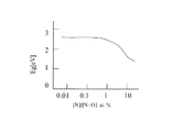
オキシナイトライドからなる薄膜は、膜中に含まれる窒素量を増やすと光学バンドギャップが小さくなり、可視光(近紫外光)の吸収を示すようになる。 図4はさまざまなZn―In―O―N系オキシナイトライド薄膜の光学バンドギャップとN/(N+O)組成比の相関を示した図である。Nは窒素原子の数、Oは酸素原子の数を示す。N/(N+O)組成比が1%(つまり、N/(N+O)=0.01)を超えると、光学バンドギャップが小さくなり、近紫外域の吸収を示すようになることがわかる。たとえば、Zn―In―Oからなる酸化物半導体チャンネルを用いたTFTにおいては、Zn−In−O−Nからなるオキシナイトライド電極のN/(N+O)組成比を0.01以上にすることで、近紫外光に起因したTFT特性変動を抑制できる。すなわち、オキシナイトライドからなるソース電極及びドレイン電極を有する薄膜トランジスタにおいて、オキシナイトライド薄膜のN/(N+O)組成比を0.01以上にすることが好ましい。 A thin film made of oxynitride has a reduced optical band gap when the amount of nitrogen contained in the film is increased, and exhibits absorption of visible light (near ultraviolet light). FIG. 4 shows the correlation between the optical band gap and the N / (N + O) composition ratio of various Zn—In—O—N oxynitride thin films. N represents the number of nitrogen atoms, and O represents the number of oxygen atoms. It can be seen that when the N / (N + O) composition ratio exceeds 1% (that is, N / (N + O) = 0.01), the optical band gap becomes small and absorption in the near ultraviolet region is exhibited. For example, in a TFT using an oxide semiconductor channel made of Zn—In—O, the N / (N + O) composition ratio of the oxynitride electrode made of Zn—In—O—N is set to 0.01 or more. , TFT characteristic fluctuations caused by near-ultraviolet light can be suppressed. That is, in a thin film transistor having a source electrode and a drain electrode made of oxynitride, it is preferable that the N / (N + O) composition ratio of the oxynitride thin film is 0.01 or more.
上述したように、酸化物半導体に影響を与える光を吸収する観点から、オキシナイトライドからなる電極の光学バンドギャップが酸化物半導体の光学バンドギャップよりも小さいことが好ましい。たとえば、アモルファス構造を有するInGaZnO4は光学バンドギャップが2.9eV程度で可視光に対して透明であるが、アモルファス構造を有するInGaZnO4をチャンネルに用いたトランジスタは、2.7eV程度以上の近紫外光が照射されると、特性が変化する場合がある。このような観点から、酸化物半導体の光学バンドギャップが、オキシナイトライドからなる電極の光学バンドギャップがより0.2eV以上、さらに好ましくは0.5eV以上、大きいことが好ましい。(以後「アモルファス構造を有する」を単にアモルファスと記載する。) As described above, from the viewpoint of absorbing light that affects the oxide semiconductor, the optical band gap of the electrode made of oxynitride is preferably smaller than the optical band gap of the oxide semiconductor. For example, InGaZnO 4 having an amorphous structure has an optical band gap of about 2.9 eV and is transparent to visible light. However, a transistor using an amorphous structure of InGaZnO 4 for a channel has a near ultraviolet of about 2.7 eV or more. When irradiated with light, the characteristics may change. From such a viewpoint, it is preferable that the optical band gap of the oxide semiconductor is larger than that of the electrode made of oxynitride by 0.2 eV or more, more preferably 0.5 eV or more. (Hereinafter, “having an amorphous structure” is simply referred to as amorphous.)
光学バンドギャップは、薄膜の分光特性(透過スペクトル)を分光光度計で評価し、その光吸収端から求めることができる。本明細書中では、光波長を800nmから短波長側にスキャンしながら光吸収係数を評価し、光吸収係数が104(1/cm)以上になる波長を光吸収端波長としている。さらに、光吸収端波長をエネルギー単位(eV)に変換することで光学バンドギャップとしている。 The optical band gap can be obtained from the light absorption edge of a thin film by evaluating the spectral characteristics (transmission spectrum) with a spectrophotometer. In this specification, the light absorption coefficient is evaluated while scanning the light wavelength from 800 nm to the short wavelength side, and the wavelength at which the light absorption coefficient is 10 4 (1 / cm) or more is defined as the light absorption edge wavelength. Furthermore, the optical band gap is obtained by converting the light absorption edge wavelength into energy units (eV).
(オキシナイトライド膜の作成方法)
オキシナイトライド薄膜の形成方法としては、酸化物薄膜を形成後に窒素を添加する方法や直接オキシナイトライド膜を形成する方法が挙げられる。
前者としては、たとえば酸化物薄膜中にイオン注入により所望の窒素を薄膜中に注入することができる。イオン注入において用いるイオン種としては、N+イオン、N-イオン、N2 +イオン(窒素分子イオン)などを用いることができる。
本発明者らは、アモルファス酸化物半導体薄膜に、窒素を添加することで酸化物薄膜の電気伝導度が大きくなることを見出した。このようにして形成されたオキシナイトライド薄膜は、電極として用いるのに十分な電気伝導度を有する。
(Oxynitride film creation method)
Examples of the method for forming an oxynitride thin film include a method of adding nitrogen after forming an oxide thin film and a method of directly forming an oxynitride film.
As the former, for example, desired nitrogen can be implanted into the thin film by ion implantation into the oxide thin film. As ion species used in the ion implantation, N + ions, N − ions, N 2 + ions (nitrogen molecular ions) and the like can be used.
The present inventors have found that the electrical conductivity of an oxide thin film is increased by adding nitrogen to the amorphous oxide semiconductor thin film. The oxynitride thin film thus formed has sufficient electrical conductivity to be used as an electrode.
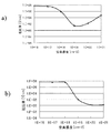
図3a)は、膜厚がおよそ400nmのInGaZnO4薄膜に、窒素をイオン注入した際の、イオン注入量に対する電気伝導率の変化を示している。図3b)は、膜厚がおよそ400nmのZn−In−O薄膜(ZnとInの組成比はZn:In=6:4)に、窒素をイオン注入した際の、イオン注入量に対する電気伝導率の変化を示している。横軸は、単位体積あたりの窒素イオンの注入量(窒素濃度)、縦軸は抵抗率である。膜中窒素濃度に対する抵抗率の変化は、酸化物薄膜の組成や膜質などに依存する。
たとえば、図3a)に示すように、1E+8Ωcm程度のInGaZnO4薄膜に、体積あたり1019(1/cm3)程度の窒素イオンを注入することで数10Ωcm程度の抵抗率の膜とすることができる。さらに、図3b)に示すように、1E+8Ωcm程度のZn−In−O系薄膜に、体積あたり1019(1/cm3)程度の窒素イオンを注入することで100Ωcm程度の抵抗率の膜を得ることができる。さらには体積あたり1020(1/cm3)程度の窒素イオンを注入することで10Ωcm程度の抵抗率の膜とすることができる。窒素の濃度範囲は、1019(1/cm3)程以上とすることで、ソース電極及びドレイン電極として用いることが可能となる。
FIG. 3a) shows the change in electrical conductivity with respect to the amount of ion implantation when nitrogen is ion-implanted into an InGaZnO 4 thin film having a thickness of about 400 nm. FIG. 3b) shows the electric conductivity with respect to the ion implantation amount when nitrogen is ion-implanted into a Zn—In—O thin film having a film thickness of about 400 nm (the composition ratio of Zn and In is Zn: In = 6: 4). Shows changes. The horizontal axis represents the amount of nitrogen ions implanted per unit volume (nitrogen concentration), and the vertical axis represents the resistivity. The change in resistivity with respect to the nitrogen concentration in the film depends on the composition and quality of the oxide thin film.
For example, as shown in FIG. 3a), a film having a resistivity of about several tens of ohm-cm can be obtained by implanting nitrogen ions of about 10 19 (1 / cm 3 ) per volume into an InGaZnO 4 thin film of about 1E + 8 Ωcm. . Furthermore, as shown in FIG. 3b), a film having a resistivity of about 100 Ωcm is obtained by implanting about 10 19 (1 / cm 3 ) nitrogen ions into a Zn—In—O thin film of about 1E + 8 Ωcm. be able to. Furthermore, a film having a resistivity of about 10 Ωcm can be obtained by implanting nitrogen ions of about 10 20 (1 / cm 3 ) per volume. When the concentration range of nitrogen is about 10 19 (1 / cm 3 ) or more, it can be used as a source electrode and a drain electrode.
前記のごとく、酸化物薄膜の少なくとも一部に後から窒素イオンを添加することでオキシナイトライド薄膜を形成することができる。
次に、別のオキシナイトライド薄膜の形成方法として、真空中や制御された雰囲気中で、基板上にオキシナイトライド薄膜を成膜する方法を説明する。
具体的には、オキシナイトライドの材料源を用いて成膜する手法、酸化物の材料源を用いて窒素雰囲気中で成膜する手法、窒化物の材料源を用いて酸素雰囲気中で成膜する手法があげられる。他にも、金属の材料源を用いて、酸素や窒素さらにはその混合雰囲気中で成膜することができる。たとえば、In2O3,ZnO,GaNの3つのターゲットを用いて同時スパッタ成膜することで、又はInGaZnO4のターゲットを用いて窒素含有雰囲気中で成膜することで、In−Ga−Zn−O−N膜を形成することができる。他にもIn2O3とZnOのターゲットを用いて、窒素含有雰囲気中で同時スパッタ成膜することで、Zn−In−O−N膜を形成することができる。Zn−In−O−N膜においては、このような手法により、抵抗率が10のマイナス3乗台の小さな抵抗率(単位:Ωcm)が得ることができる。例えば1mΩcm(1×10⁻³Ωcm)から10mΩcmの膜を得ることができる。これらは、電極として用いるのに十分な電気伝導率を有している。
ここではスパッタ法について説明したが、パルスレーザー蒸着法(PLD法)、及び電子ビーム蒸着法などの気相法を用いることができる。成膜中にラジカル源等を用いてNラジカルを照射することも、膜中窒素濃度を大きくしたい場合に効果的である。しかし、成膜法は、これらの方法に限られるのものではない。
必要であれば、オキシナイトライド電極上にさらに電気伝導度の高い薄膜を配しても良い。これにより良好な半導体―オキシナイトライド電極間の電気コンタクトと、電極内で生じる直列抵抗を小さくすることができる。
As described above, the oxynitride thin film can be formed by adding nitrogen ions to at least a part of the oxide thin film later.
Next, as another method for forming an oxynitride thin film, a method for forming an oxynitride thin film on a substrate in a vacuum or in a controlled atmosphere will be described.
Specifically, film formation using an oxynitride material source, film formation in a nitrogen atmosphere using an oxide material source, film formation in an oxygen atmosphere using a nitride material source The technique to do is given. In addition, a metal material source can be used to form a film in oxygen, nitrogen, or a mixed atmosphere thereof. For example, In—Ga—Zn— can be formed by simultaneous sputtering deposition using three targets of In 2 O 3 , ZnO, and GaN, or by deposition in a nitrogen-containing atmosphere using a target of InGaZnO 4. An O—N film can be formed. In addition, a Zn—In—O—N film can be formed by simultaneous sputtering deposition in a nitrogen-containing atmosphere using an In 2 O 3 and ZnO target. With a Zn—In—O—N film, a small resistivity (unit: Ωcm) with a resistivity of 10 minus the third power can be obtained by such a method. For example, a film of 1 mΩcm (1 × 10 −3 Ωcm) to 10 mΩcm can be obtained. These have sufficient electrical conductivity to be used as electrodes.
Although the sputtering method has been described here, a gas phase method such as a pulse laser deposition method (PLD method) or an electron beam deposition method can be used. Irradiation with N radicals using a radical source or the like during film formation is also effective when it is desired to increase the nitrogen concentration in the film. However, the film forming method is not limited to these methods.
If necessary, a thin film having higher electrical conductivity may be disposed on the oxynitride electrode. This makes it possible to reduce the electrical contact between the semiconductor-oxynitride electrode and the series resistance generated in the electrode.
(チャンネル層) チャンネル層の材料は、酸化物であればどのような材料も用いることができるが、大きな移動度を得ることができるInやZn系の酸化物が挙げられる。たとえば、In−Ga−Zn―O系やZn−In−O系、Zn−Sn−O系のアモルファス酸化物や、ZnOやIn2O3などの結晶性酸化物などがあげられる。特に、チャンネル層はアモルファスの酸化物からなることが好ましい。ZnOなどの多結晶薄膜を用いると多結晶粒子の形状や相互接続が成膜方法により大きく異なるため、TFT素子の特性がばらついてしまうからである。さらには、InとGaとZnを含有したアモルファス酸化物からなることが、特に、好ましい。すなわちIn−Ga−Zn−O膜やZn−In−O膜が好適である。 アモルファス酸化物は、成膜条件(成膜時の雰囲気、温度、成膜レートなど)やアニール条件などによりその電気伝導度を制御することができる。0.1S/cm以下の電気伝導度を有したアモルファス酸化物半導体膜をチャンネルに適用することができる。チャンネルは、良好な半導体特性を示すものであれば窒素を含有した酸化物であっても良い。 (Channel Layer) Any material can be used as the material of the channel layer as long as it is an oxide, and examples thereof include In and Zn-based oxides that can obtain high mobility. For example, an In—Ga—Zn—O-based, Zn—In—O-based, or Zn—Sn—O-based amorphous oxide, or a crystalline oxide such as ZnO or In 2 O 3 can be given. In particular, the channel layer is preferably made of an amorphous oxide. This is because when a polycrystalline thin film such as ZnO is used, the shape and interconnection of the polycrystalline particles vary greatly depending on the film forming method, and the characteristics of the TFT element vary. Further, it is particularly preferable to be made of an amorphous oxide containing In, Ga, and Zn. That is, an In—Ga—Zn—O film or a Zn—In—O film is preferable. The electrical conductivity of the amorphous oxide can be controlled by film formation conditions (atmosphere during film formation, temperature, film formation rate, etc.) and annealing conditions. An amorphous oxide semiconductor film having an electric conductivity of 0.1 S / cm or less can be applied to the channel. The channel may be an oxide containing nitrogen as long as it exhibits good semiconductor characteristics.
(ゲート電極)
ゲート電極15は、たとえば、In2O3:Sn、ZnOなどの透明導電膜や、Au、Pt、Al、Niなどの金属膜を用いることができる。上述のソース電極及びドレイン電極と同様にオキシナイトライドからなる膜を用いても良い。
(Gate electrode)
For the
(ゲート絶縁層)
ゲート絶縁層12の材料は良好な絶縁性を有するものであれば、特に材料は限定されない。たとえば、ゲート絶縁層12としては、SiO2、Al2O3、Y2O3、又はHfO2の1種、又はそれらの化合物を少なくとも二種以上含む混晶化合物を用いることができる。これにより、ソース・ゲート電極間及びドレイン・ゲート電極間のリーク電流を約10−10(A)以下にすることができる。
(Gate insulation layer)
The material of the
(基板)
基板10としては、ガラス基板、プラスチック基板、プラスチックフィルムなどを用いることができる。
(substrate)
As the
(TFT特性)
図5に本発明の電界効果型トランジスタの典型的な特性を示す。ソース・ドレイン電極間に5〜15V程度の電圧Vdを印加したとき、ゲート電圧Vgの印加を0Vと10Vの間でオン・オフすることで、ソース・ドレイン電極間の電流Idを制御する(オン・オフする)ことができる。図5a)はさまざまなVgでのId−Vd特性、図5b)はVd=10VにおけるId−Vg特性(トランスファ特性)の例である。TFT特性の評価には、オン・オフ比や電界効果移動度が用いられる。オン・オフ比は、オン時のIdとオフ時のIdの比から求める。電界効果移動度は√Id−Vgのグラフを作成し、その傾きから見積もることができる。
(TFT characteristics)
FIG. 5 shows typical characteristics of the field effect transistor of the present invention. When a voltage Vd of about 5 to 15 V is applied between the source and drain electrodes, the gate voltage Vg is turned on and off between 0 V and 10 V to control the current Id between the source and drain electrodes (on・ It can be turned off. FIG. 5a) is an example of Id-Vd characteristics at various Vg, and FIG. 5b) is an example of Id-Vg characteristics (transfer characteristics) at Vd = 10V. For evaluation of TFT characteristics, an on / off ratio and field effect mobility are used. The on / off ratio is obtained from the ratio of Id at the on time to Id at the off time. The field effect mobility can be estimated from a slope of √Id−Vg.
本実施例は、図1a)に示すトップゲート型TFTの例である。チャンネル層11にIn−Ga−Zn−O系のアモルファス酸化物半導体を用い、ソース電極13及びドレイン電極14にIn―Ga―Zn―O―N系のオキシナイトライド膜を用いている。このようなTFTを製造する工程を以下に説明する。
まず、ガラス基板10(コーニング社製1737)上にチャンネル層としてアモルファス酸化物半導体膜11を形成する。本実施例では、アルゴンガスと酸素ガスとの混合雰囲気中で高周波スパッタ法により、In−Ga−Zn−O系アモルファス酸化物膜を形成する。
ターゲット(材料源)としては、2インチサイズのInGaZnO4組成を有する多結晶焼結体を用い、投入RFパワーは100Wとしている。成膜時の雰囲気は、全圧0.45Paであり、ガス流量比としてAr:O2=100:1である。成膜レートは12nm/minである。また、基板温度は25℃であり、成膜後に280℃で40分間のアニールを行う。膜厚は約30nmであり、蛍光X線(XRF)分析によると、薄膜の金属組成比はIn:Ga:Zn=35:35:30である。X線回折で評価すると、明瞭なピークは存在せず、薄膜はアモルファスである。
This example is an example of a top gate type TFT shown in FIG. An In—Ga—Zn—O-based amorphous oxide semiconductor is used for the channel layer 11, and an In—Ga—Zn—O—N-based oxynitride film is used for the source electrode 13 and the drain electrode 14. A process for manufacturing such a TFT will be described below.
First, an amorphous oxide semiconductor film 11 is formed as a channel layer on a glass substrate 10 (Corning 1737). In this embodiment, an In—Ga—Zn—O-based amorphous oxide film is formed by high-frequency sputtering in a mixed atmosphere of argon gas and oxygen gas.
As a target (material source), a polycrystalline sintered body having a 2-inch size InGaZnO 4 composition is used, and the input RF power is 100 W. The atmosphere during film formation is a total pressure of 0.45 Pa, and the gas flow rate ratio is Ar: O 2 = 100: 1. The film formation rate is 12 nm / min. The substrate temperature is 25 ° C., and annealing is performed at 280 ° C. for 40 minutes after film formation. The film thickness is about 30 nm, and according to fluorescent X-ray (XRF) analysis, the metal composition ratio of the thin film is In: Ga: Zn = 35: 35: 30. When evaluated by X-ray diffraction, there is no clear peak and the thin film is amorphous.
次に、オキシナイトライドからなる、ドレイン電極14及びソース電極13を形成する。パターン形成には、フォトリソグラフィー法とリフトオフ法を用いている。ソース電極及びドレイン電極はIn―Ga―Zn―O―N膜からなり、厚さ100nmである。
オキシナイトライド膜の成膜には、図6に示すようなスパッタ成膜装置を用いている。
図6において、51は試料、52はターゲット、53は真空ポンプ、54は真空計、55は基板保持手段、56はそれぞれのガス導入系に対して設けられたガス流量制御手段、57は圧力制御手段、58は成膜室である。
真空ポンプ53は成膜室58内を排気するための排気手段となる。基板保持手段55は、基板を成膜室内に保持する。ターゲット52は、基板保持手段55に対向して配置された固体材料源である。さらに、固体材料源から材料を蒸発させるためのエネルギー源(不図示の高周波電源)と、成膜室内にガスを供給する手段を有する。ガス導入系としては、アルゴンと窒素の2系統を有している。それぞれのガス流量を独立に制御可能とするガス流量制御手段56と、排気速度を制御するための圧力制御手段57により、成膜室58の中に所定のガス雰囲気を得ることができる。
Next, the drain electrode 14 and the source electrode 13 made of oxynitride are formed. For pattern formation, a photolithography method and a lift-off method are used. The source electrode and the drain electrode are made of an In—Ga—Zn—O—N film and have a thickness of 100 nm.
A sputtering film forming apparatus as shown in FIG. 6 is used for forming the oxynitride film.
In FIG. 6, 51 is a sample, 52 is a target, 53 is a vacuum pump, 54 is a vacuum gauge, 55 is a substrate holding means, 56 is a gas flow rate control means provided for each gas introduction system, and 57 is a pressure control. Means 58 is a film forming chamber.
The
In―Ga―Zn―O―N膜の成膜には、InGaZnO4のターゲットを用いている。成膜時の全圧は0.4Paであり、ガス流量比はAr:N2=10:1である。金属組成比はIn:Ga:Zn=35:36:29であり、N/O比は0.1である。抵抗率は約0.1Ωcmと見積もっている。X線回折で評価すると、明瞭なピークは存在せず、薄膜はアモルファスである。
次に、ゲート絶縁層12を形成する。ゲート絶縁層12は、SiOx膜をスパッタ成膜法により成膜し、厚みは150nmである。またSiOx膜の比誘電率は約3.7である。
さらに、ゲート電極15を形成する。電極材質はMoであり、厚さは100nmである。薄膜トランジスタのチャンネル長は、50μmで、チャンネル幅は、200μmである。
An InGaZnO 4 target is used to form the In—Ga—Zn—O—N film. The total pressure during film formation is 0.4 Pa, and the gas flow ratio is Ar: N 2 = 10: 1. The metal composition ratio is In: Ga: Zn = 35: 36: 29, and the N / O ratio is 0.1. The resistivity is estimated to be about 0.1 Ωcm. When evaluated by X-ray diffraction, there is no clear peak and the thin film is amorphous.
Next, the
Further, the
(特性評価)
TFT特性を評価すると、閾値は約+1.5Vであり、オン・オフ比は109、電界効果移動度は約8cm2(Vs)−1である。オキシナイトライド電極と酸化物半導体の接触抵抗を見積もると、2x10⁻⁴Ωcm2程度であり、良好なオーミック接続が得られている。オーミック接続とは、電流−電圧特性が直線又は略直線となる接続を意味する。また、接触抵抗の素子間ばらつきが小さく、これにより、TFT素子の特性ばらつきも小さい。このように、In−Ga−Zn−O―Nというオキシナイトライドからなるソース電極及びドレイン電極を適用することで、良好なトランジスタ特性を実現することができる。
チャンネルを構成するアモルファス酸化物InGaZnO4の光学バンドギャップが2.9eVであるのに対し、オキシナイトライド膜の光学バンドギャップは2.6eVである。すなわち、In―Ga―Zn―O―N膜(オキシナイトライド膜)は、チャンネルに影響を与えうる近紫外光(波長450nm以下の光)を十分に吸収する。このようなオキシナイトライド膜からなる電極を用いることで、電極からチャンネルへの近紫外光の入射を抑制することができる。すなわち、光に対して安定なTFT基板を作成できる。
光照射に対して安定な特性を有した電界効果トランジスタは、有機発光ダイオードの動作回路への利用などが期待できる。
(Characteristic evaluation)
When the TFT characteristics are evaluated, the threshold is about +1.5 V, the on / off ratio is 10 9 , and the field-effect mobility is about 8 cm 2 (Vs) −1 . When the contact resistance between the oxynitride electrode and the oxide semiconductor is estimated, it is about 2 × 10 −4 Ωcm 2 , and a good ohmic connection is obtained. The ohmic connection means a connection in which the current-voltage characteristic is a straight line or a substantially straight line. In addition, the variation in contact resistance between elements is small, and thus the characteristic variation in TFT elements is also small. In this manner, favorable transistor characteristics can be realized by using a source electrode and a drain electrode formed of oxynitride of In—Ga—Zn—O—N.
The optical band gap of the amorphous oxide InGaZnO 4 constituting the channel is 2.9 eV, whereas the optical band gap of the oxynitride film is 2.6 eV. That is, the In—Ga—Zn—O—N film (oxynitride film) sufficiently absorbs near-ultraviolet light (light having a wavelength of 450 nm or less) that can affect the channel. By using an electrode made of such an oxynitride film, incidence of near ultraviolet light from the electrode to the channel can be suppressed. That is, a TFT substrate that is stable against light can be produced.
A field effect transistor having stable characteristics against light irradiation can be expected to be used in an operation circuit of an organic light emitting diode.
本実施例は、図1b)に示すボトムゲート型TFTの例である。チャンネル層11にはZn―In−O系のアモルファス酸化物を用い、ソース電極13及びドレイン電極14には、Zn―In−O―N系のオキシナイトライド膜を用いている。このようなTFTを製造する工程を以下に説明する。
まず、ガラス基板(コーニング社製1737)上にゲート電極として厚さ100nmのMo膜をスパッタ法により形成する。
次に、ゲート電極絶縁層12として厚さ150nmのSiOx膜をスパッタ法により形成する。
引き続き、チャンネル層としてZn―In−O系アモルファス酸化物半導体膜を、ZnOとIn2O3のターゲットを用いた同時スパッタリングの手法により形成する。アルゴンと酸素の混合比はAr:O2=80:1である。成膜レートは12nm/minである。また、基板温度は25℃である。膜厚は約30nmである。作製したZn−In−O膜はアモルファスであり、金属組成比率はZn:In=64:36である。X線回折で評価すると、明瞭なピークは存在せず、薄膜はアモルファスである。
This example is an example of a bottom gate type TFT shown in FIG. A Zn—In—O-based amorphous oxide is used for the channel layer 11, and a Zn—In—O—N-based oxynitride film is used for the source electrode 13 and the drain electrode 14. A process for manufacturing such a TFT will be described below.
First, a Mo film having a thickness of 100 nm is formed by sputtering as a gate electrode on a glass substrate (Corning 1737).
Next, a 150 nm thick SiOx film is formed as the gate
Subsequently, a Zn—In—O amorphous oxide semiconductor film is formed as a channel layer by a co-sputtering technique using ZnO and In 2 O 3 targets. The mixing ratio of argon and oxygen is Ar: O 2 = 80: 1. The film formation rate is 12 nm / min. The substrate temperature is 25 ° C. The film thickness is about 30 nm. The manufactured Zn—In—O film is amorphous, and the metal composition ratio is Zn: In = 64: 36. When evaluated by X-ray diffraction, there is no clear peak and the thin film is amorphous.
次に、オキシナイトライドからなる、ドレイン電極14及びソース電極13を形成する。電極はZn―In−O―N膜からなり、厚さ150nmである。Zn―In−O―N膜の成膜には、ZnOとInを用いた同時スパッタリングの手法を用いている。成膜時の全圧は0.4Paであり、ガス流量比はAr:N2=1:1である。また、窒素ガスはラジカル源を用い、電子サイクロトロン共鳴プラズマにより励起している。金属組成比はZn:Inは61:39であり、N:Oは6:4程度である。抵抗率は約10mΩcmであり、電極として用いるのに十分に低い値を有している。本実施例のオキシナイトライド薄膜は、X線回折の評価によると結晶構造を有した多結晶膜からなっており、これが低い抵抗率の一因であると考えられる。 Next, the drain electrode 14 and the source electrode 13 made of oxynitride are formed. The electrode is made of a Zn—In—O—N film and has a thickness of 150 nm. For the formation of the Zn—In—O—N film, a simultaneous sputtering method using ZnO and In is used. The total pressure during film formation is 0.4 Pa, and the gas flow ratio is Ar: N 2 = 1: 1. Nitrogen gas is excited by electron cyclotron resonance plasma using a radical source. The metal composition ratio is about 61:39 for Zn: In and about 6: 4 for N: O. The resistivity is about 10 mΩcm, which is a value low enough to be used as an electrode. The oxynitride thin film of this example consists of a polycrystalline film having a crystal structure according to the evaluation of X-ray diffraction, and this is considered to be a cause of low resistivity.
(特性評価)
TFT特性を評価すると、閾値は約0.5Vであり、オン・オフ比が109、電界効果移動度は約16cm2(Vs)−1である。オキシナイトライド電極と酸化物半導体の接触抵抗を見積もると、1x10⁻⁴Ωcm2程度であり、良好なオーミック接続が得られる。また、接触抵抗のばらつきが小さく、TFT素子の特性ばらつきも小さい。
このように、Zn―In−O―Nというオキシナイトライドからなるソース電極及びドレイン電極とアモルファスZn−In−O半導体を適用することで、良好なトランジスタ特性を実現することができる。
チャンネルを構成するアモルファス酸化物Zn―In−Oの光学バンドギャップが2.6eVであるのに対し、オキシナイトライド膜(Zn−In−O−N膜)の光学バンドギャップは1.6eVである。すなわち、Zn―In−O―N膜は、チャンネルに影響を与えうる近紫外光を十分に吸収する。このようなオキシナイトライドからなる電極を用いることで、電極からチャンネルへの近紫外光の入射を抑制することができる。すなわち、光に対して安定なTFT基板を作成できる。
光照射に対して安定な特性を有した電界効果トランジスタは、有機発光ダイオードの動作回路への利用などが期待できる。
(Characteristic evaluation)
When the TFT characteristics are evaluated, the threshold is about 0.5 V, the on / off ratio is 10 9 , and the field-effect mobility is about 16 cm 2 (Vs) −1 . When the contact resistance between the oxynitride electrode and the oxide semiconductor is estimated, it is about 1 × 10 −4 Ωcm 2 , and a good ohmic connection can be obtained. In addition, variations in contact resistance are small, and variations in characteristics of TFT elements are also small.
As described above, by using the source electrode and the drain electrode made of oxynitride called Zn—In—O—N and the amorphous Zn—In—O semiconductor, good transistor characteristics can be realized.
The optical band gap of the amorphous oxide Zn—In—O constituting the channel is 2.6 eV, whereas the optical band gap of the oxynitride film (Zn—In—O—N film) is 1.6 eV. . That is, the Zn—In—O—N film sufficiently absorbs near ultraviolet light that can affect the channel. By using such an electrode made of oxynitride, it is possible to suppress the near ultraviolet light from entering the channel from the electrode. That is, a TFT substrate that is stable against light can be produced.
A field effect transistor having stable characteristics against light irradiation can be expected to be used in an operation circuit of an organic light emitting diode.
本実施例は、図2に示すコプレーナ型の電界効果型トランジスタの例である。図2は断面図であり、図において10は基板、11はチャンネル層(酸化物薄膜)、12はゲート絶縁層、15はゲート電極、である。チャンネル層11の中には、窒素が添加されたソース部位16(実施例1におけるソース電極に相当)、窒素が添加されたドレイン部位17(実施例1におけるドレイン電極に相当)、チャンネル部位18(実施例1におけるチャンネル層に相当)がある。 チャンネル層11にIn−Ga―Zn−O系のアモルファス酸化物を用い、電極であるソース部位16、ドレイン部位17の形成には、窒素のイオン注入の手法を用いている。また、図7において、ソース部位、ドレイン部位の形成方法を記している。このようなトランジスタを製造する工程を以下に説明する。
This embodiment is an example of a coplanar field effect transistor shown in FIG. 2 is a cross-sectional view, in which 10 is a substrate, 11 is a channel layer (oxide thin film), 12 is a gate insulating layer, and 15 is a gate electrode. In the channel layer 11, a
まず、ガラス基板10(コーニング社製1737)上にチャンネル層11としてアモルファス酸化物膜を形成する。 本実施例では、アルゴンガスと酸素ガスとの混合雰囲気中で高周波スパッタ法により、In−Zn−Ga−O系アモルファス酸化物膜を形成する。ターゲット(材料源)としては、2インチサイズのInGaZnO4組成を有する多結晶焼結体を用い、投入RFパワーは100Wとする。成膜時の雰囲気は、全圧は0.45Paであり、その際ガス流量比はAr:O2=80:1である。成膜レートは11nm/minである。また、基板温度は25℃である。膜厚は約50nmであり、蛍光X線分析の結果、薄膜の金属組成比はIn:Ga:Zn=36:35:29である。X線回折で評価すると、明瞭なピークは存在せず、薄膜はアモルファスである。 First, an amorphous oxide film is formed as a channel layer 11 on a glass substrate 10 (Corning 1737). In this embodiment, an In—Zn—Ga—O-based amorphous oxide film is formed by high-frequency sputtering in a mixed atmosphere of argon gas and oxygen gas. As a target (material source), a polycrystalline sintered body having a 2-inch size InGaZnO 4 composition is used, and the input RF power is 100 W. As for the atmosphere during film formation, the total pressure is 0.45 Pa, and the gas flow rate ratio is Ar: O 2 = 80: 1. The film formation rate is 11 nm / min. The substrate temperature is 25 ° C. The film thickness is about 50 nm, and as a result of fluorescent X-ray analysis, the metal composition ratio of the thin film is In: Ga: Zn = 36: 35: 29. When evaluated by X-ray diffraction, there is no clear peak and the thin film is amorphous.
次に、ゲート絶縁層12をパターニング形成する。ゲート絶縁層12は、SiOx膜をスパッタ法により成膜し、厚みは150nmである。 さらに、Moからなる厚さ100nmのゲート電極15を形成する。 次に、アモルファス酸化物薄膜11に窒素イオン注入を行い(図7a))、チャンネル層11の中に、ソース部位16及びドレイン部位17を形成する(図7b))。イオン注入において、図7に示すように窒素イオンは、ゲート絶縁層12を介してチャンネル層(酸化物薄膜)11の中に注入される。このような手法によって、ゲート電極15がマスクとなり、ゲート電極のパターンに対応して、N注入されたソース部位16、ドレイン部位17が自己整合的に配置される。 イオン注入に際しては、イオン種としてN+を用い、加速電圧は30kVである。ソース部位16及びドレイン部位17の窒素濃度は2x10¹⁹(1/cm3)程度である。また、別途、同様な条件でN注入された試料の抵抗率を評価すると、10Ωcm程度である。 さらに、図7c)に示すように、SiO2からなる絶縁層19とMoからなる埋め込み配線20、21を形成した。最後に300℃で20分間のアニールを行っている。チャンネル部位18の長さは、40μmで、チャンネル部位18の幅は、200μmである。電極材質はMoであり、厚さは100nmである。
Next, the
(TFT素子の特性評価) TFT特性を評価すると、閾値は約1Vであり、オン・オフ比は109、電界効果移動度は約9cm2(Vs)−1である。オキシナイトライド電極と酸化物半導体の接触抵抗を見積もると、8x10⁻⁵Ωcm2程度であり、良好なオーミック接続が得られる。また、接触抵抗のばらつきが小さく、TFT素子の特性ばらつきも小さい。 本実施例の電界効果トランジスタは、チャンネル層(酸化物薄膜)11の中に、チャンネル部位18と、チャンネル部位18に比べて窒素濃度の大きなソース部位16及びドレイン部位17を有している。ソース部位16とドレイン部位17に窒素を添加することで、チャンネル部位18よりも電気伝導率が大きくなっている。このようにチャンネル部位18とほぼ同一の材料系でソース部位16及びドレイン部位17を構成することで、チャンネル部位18とソース用の配線20、ドレイン用の配線21に良好な電気的な接続を実現できる。すなわち、配線20、配線21は、ソース部位16、ドレイン部位17を介して、チャンネル部位18と接続されることで、良好な電気接続がなされる。これにより、チャンネル部位18と配線20、配線21との間で、安定な電気接続が可能となり、素子の均一性、信頼性が向上すると考えられる。
(Characteristic evaluation of TFT element) When the TFT characteristic is evaluated, the threshold value is about 1 V, the on / off ratio is 10 9 , and the field-effect mobility is about 9 cm 2 (Vs) −1 . When the contact resistance between the oxynitride electrode and the oxide semiconductor is estimated, it is about 8 × 10 −5 Ωcm 2 , and a good ohmic connection can be obtained. In addition, variations in contact resistance are small, and variations in characteristics of TFT elements are also small. The field effect transistor of this embodiment has a channel part (oxide thin film) 11 having a
また、本実施例のTFTは、ヒステリシス特性も良好である(ヒステリシスが小さい)。ヒステリシスとは、TFTトランスファ特性の評価において、ソース・ドレイン電極間の電圧Vdを固定して、ゲート電圧Vgを掃引(上下)させた際に、ゲート電圧Vgの上昇時と下降時でソース・ドレイン電極間の電流Idが異なる値を示すことを言う。ヒステリシスが大きいと、設定したVgに対して得られるIdの値がばらついてしまうため、ヒステリシスが小さい素子が好ましい。本実施例では、ソース、ドレイン電極とチャンネルの間で、チャージがトラップされにくい良好な電気接続が実現できるため、ヒステリシスが小さい薄膜トランジスタとなっている。 Further, the TFT of this example also has good hysteresis characteristics (small hysteresis). In the evaluation of TFT transfer characteristics, hysteresis means that when the gate voltage Vg rises and falls when the voltage Vd between the source and drain electrodes is fixed and the gate voltage Vg is swept (up and down), It means that the current Id between the electrodes shows different values. If the hysteresis is large, the value of Id obtained with respect to the set Vg varies. Therefore, an element having a small hysteresis is preferable. In this embodiment, since a good electrical connection in which charge is not easily trapped between the source and drain electrodes and the channel can be realized, the thin film transistor has a small hysteresis.
本実施例のTFTは動特性が良好である。ソース、ドレイン間に5Vを印加し、ゲート電極に+5Vおよび−5Vの電圧を交互にパルス幅30μsec、周期30msecで切り替えて印加し、ドレイン電流の応答を測定すると、電流立ち上がりに優れ、さらに立ち上がり時間の素子間ばらつきが小さい。本実施例においては自己整合的な手法を用いることで、ソース部位とゲート電極の重なり及びドレイン部位とゲート電極の重なりが小さく、さらにこの重なりが均一なトランジスタを実現できる。この結果、ソース部位とゲート電極のオーバーラップ部及びドレイン部位とゲート電極のオーバーラップ部に形成されるトランジスタの寄生容量を小さく、さらには均一にすることができる。寄生容量が小さいために、高速動作が可能となる。また寄生容量が均一であるために、特性の均一性に優れたトランジスタを実現できる。すなわち、本実施例において、自己整合的な手法により、ゲート電極、ソース部位、及びドレイン部位の位置関係を精度良く作成できたことで、高速動作が可能であるとともに、均一性が高い素子を実現できる。 The TFT of this example has good dynamic characteristics. When 5V is applied between the source and drain, + 5V and -5V are alternately applied to the gate electrode with a pulse width of 30 μsec and a cycle of 30 msec, and the response of the drain current is measured, the current rise is excellent and the rise time is further improved. The variation between elements is small. In this embodiment, by using a self-alignment technique, a transistor in which the overlap between the source region and the gate electrode and the overlap between the drain region and the gate electrode are small and the overlap is uniform can be realized. As a result, the parasitic capacitance of the transistors formed in the overlap portion between the source portion and the gate electrode and the overlap portion between the drain portion and the gate electrode can be reduced and made uniform. Since the parasitic capacitance is small, high-speed operation is possible. Further, since the parasitic capacitance is uniform, a transistor having excellent characteristic uniformity can be realized. In other words, in this embodiment, the self-aligned technique enables the positional relationship between the gate electrode, the source region, and the drain region to be created with high accuracy, thereby realizing high-speed operation and highly uniform elements. it can.
本発明者らは、特開2007−250983において、酸化物半導体において水素又は重水素が添加されたソース部を設けることで、良好な電気接続が可能であることを技術開示している。しかしながら水素を添加した電極部(ソース部)を配した構成においては、たとえば350℃程度以上の高温での熱処理を行った場合に、TFT特性にばらつきが生じる場合がある。原因は定かではないが、水素が酸化物半導体中を拡散するためであると考えることができる。 一方、本発明の窒素を添加した電極部(ソース部)を配した構成においては熱処理下によるTFT特性のばらつきが小さい。窒素の酸化物半導体中の拡散が遅いために、温度耐性の高い電気接続が実現できる。 本発明の酸化物半導体と電極との接合性に優れた電界効果トランジスタは、有機発光ダイオードの動作回路への利用などが期待できる。 In Japanese Patent Application Laid-Open No. 2007-250983, the present inventors have disclosed that a good electrical connection is possible by providing a source portion to which hydrogen or deuterium is added in an oxide semiconductor. However, in the configuration in which the electrode portion (source portion) to which hydrogen is added is arranged, the TFT characteristics may vary when a heat treatment is performed at a high temperature of, for example, about 350 ° C. or more. Although the cause is not clear, it can be considered that hydrogen is diffused in the oxide semiconductor. On the other hand, in the configuration in which the electrode portion (source portion) to which nitrogen is added according to the present invention is arranged, variation in TFT characteristics due to heat treatment is small. Since the diffusion of nitrogen in the oxide semiconductor is slow, an electrical connection with high temperature resistance can be realized. The field effect transistor excellent in bondability between the oxide semiconductor and the electrode of the present invention can be expected to be used for an operation circuit of an organic light emitting diode.
本実施例は、図1b)に示すボトムゲート型TFT素子の例である。チャンネル層11にZnOからなる結晶性を有した酸化物半導体を用い、ソース電極13及びドレイン電極14にZn―In―O―Nからなる結晶性を有したオキシナイトライドを用いる例である。また、ゲート電極15にもオキシナイトライド膜を用いている。
まず、ガラス基板(コーニング社製1737)10の上にゲート電極15として厚さ100nmのZn−In−O−N膜をスパッタ法により形成する。成膜方法は、実施例2のZn−In−O−N膜の作成に準じている。
次に、ゲート電極絶縁層12として厚さ150nmのSiOx膜をスパッタリング法により形成する。
引き続き、スパッタリング法によりチャンネル層11として多結晶のZnO膜を形成する。ZnO焼結体ターゲットを用い、アルゴンと酸素の混合比はAr:O2=10:1である。成膜レートは12nm/minである。また、基板温度は25℃である。膜厚は約30nmである。本実施例のチャンネル層を構成するZnO膜は、ウルツ鉱型の結晶構造を有した多結晶膜からなっている。
次に、オキシナイトライドからなる、ドレイン電極14及びソース電極13を形成する。電極はZn―In−O―N膜からなり、150nmである。Zn―In−O―N膜の成膜には、ZnOとInを用いた同時スパッタリング法を用いる。成膜時の全圧は0.3Paであり、ガス流量比はAr:N2=1:1である。また、窒素ガスはラジカル源により電子サイクロトロン共鳴プラズマにより励起している。金属組成比はZn:Inは1:1程度であり、N:Oもほぼ1:1程度である。抵抗率は約3mΩcmと十分に低い値を有している。本実施例のオキシナイトライド薄膜は、X線回折の評価によると多結晶構造を有している。
This example is an example of a bottom gate type TFT device shown in FIG. This is an example in which an oxide semiconductor having crystallinity made of ZnO is used for the channel layer 11 and an oxynitride having crystallinity made of Zn—In—O—N is used for the source electrode 13 and the drain electrode 14. An oxynitride film is also used for the
First, a Zn—In—O—N film having a thickness of 100 nm is formed as a
Next, a 150 nm thick SiOx film is formed as the gate
Subsequently, a polycrystalline ZnO film is formed as the channel layer 11 by sputtering. Using a ZnO sintered compact target, the mixing ratio of argon and oxygen is Ar: O 2 = 10: 1. The film formation rate is 12 nm / min. The substrate temperature is 25 ° C. The film thickness is about 30 nm. The ZnO film constituting the channel layer of this example is a polycrystalline film having a wurtzite crystal structure.
Next, the drain electrode 14 and the source electrode 13 made of oxynitride are formed. The electrode is made of a Zn—In—O—N film and has a thickness of 150 nm. For the formation of the Zn—In—O—N film, a simultaneous sputtering method using ZnO and In is used. The total pressure during film formation is 0.3 Pa, and the gas flow rate ratio is Ar: N 2 = 1: 1. Nitrogen gas is excited by electron cyclotron resonance plasma from a radical source. The metal composition ratio is about 1: 1 for Zn: In, and about 1: 1 for N: O. The resistivity has a sufficiently low value of about 3 mΩcm. The oxynitride thin film of this example has a polycrystalline structure according to the evaluation of X-ray diffraction.
(特性評価)
TFT特性を評価すると、閾値は約0.5Vであり、オン・オフ比が107、電界効果移動度は約4cm2(Vs)−1である。オキシナイトライド電極と酸化物半導体の接触抵抗を見積もると、1x10⁻⁴Ωcm2程度であり、良好な電気接続が得られる。このように、Zn―In−O―Nというオキシナイトライドからなるソース電極及びドレイン電極と、結晶性ZnO半導体とを適用することで、良好なトランジスタ特性を実現することができる。
チャンネルを構成するZnOの光学バンドギャップが3.3eV程度であるのに対してオキシナイトライド膜(Zn−In−O−N)の光学バンドギャップは1.5eV程度である。すなわち、Zn―In−O―N膜は、チャンネルに影響を与えうる近紫外光を十分に吸収する。このようなオキシナイトライドからなる電極を用いることで、電極からチャンネルへの近紫外光の入射を抑制することができる。すなわち、光に対して安定なTFT基板を作成できる。
光照射に対して安定な特性を有する電界効果トランジスタは、有機発光ダイオードの動作回路への利用などが期待できる。
(Characteristic evaluation)
When the TFT characteristics are evaluated, the threshold is about 0.5 V, the on / off ratio is 10 7 , and the field-effect mobility is about 4 cm 2 (Vs) −1 . When the contact resistance between the oxynitride electrode and the oxide semiconductor is estimated, it is about 1 × 10 −4 Ωcm 2 , and a good electrical connection can be obtained. As described above, by using the source electrode and the drain electrode made of oxynitride called Zn—In—O—N and the crystalline ZnO semiconductor, good transistor characteristics can be realized.
The optical band gap of ZnO constituting the channel is about 3.3 eV, whereas the optical band gap of the oxynitride film (Zn—In—O—N) is about 1.5 eV. That is, the Zn—In—O—N film sufficiently absorbs near ultraviolet light that can affect the channel. By using such an electrode made of oxynitride, it is possible to suppress the near ultraviolet light from entering the channel from the electrode. That is, a TFT substrate that is stable against light can be produced.
Field effect transistors having stable characteristics with respect to light irradiation can be expected to be used in operation circuits of organic light emitting diodes.
本発明の酸化物半導体を用いた薄膜トランジスタは、低温で薄膜形成を行うことが可能で、かつ光照射環境下の安定性が高いためLCDや有機ELディスプレイのスイッチング素子として応用することができる。さらには、フレキシブル・ディスプレイをはじめ、シースルー型のディスプレイ、ICカードやIDタグなどに幅広く応用できる。 A thin film transistor using an oxide semiconductor of the present invention can be formed as a switching element for an LCD or an organic EL display because it can form a thin film at a low temperature and has high stability under a light irradiation environment. Furthermore, it can be widely applied to flexible displays, see-through displays, IC cards and ID tags.
Claims (6)
前記ゲート絶縁層は、前記チャンネル、前記ソース電極及び前記ドレイン電極と、前記ゲート電極との間に配置され、
前記チャンネルは、亜鉛(Zn)を含有する酸化物半導体からなり、
前記ソース電極またはドレイン電極は、少なくとも亜鉛(Zn)またはインジウム(In)を含有するオキシナイトライドからなり、
前記酸化物半導体に含有される金属元素は、前記オキシナイトライドに含有されていることを特徴とする電界効果型トランジスタ。 A field effect transistor having a gate electrode, a gate insulating layer, a channel, and a source electrode and a drain electrode electrically connected to the channel on a substrate,
The gate insulating layer is disposed between the channel, the source electrode and the drain electrode, and the gate electrode;
The channel is made of an oxide semiconductor containing zinc (Zn),
The source electrode or the drain electrode is made of an oxynitride having containing at least zinc (Zn) or indium (In),
The metallic element contained in the oxide semiconductor, field effect transistor, characterized in that it is contained in the oxynitride.
前記オキシナイトライドは亜鉛(Zn)とインジウム(In)と酸素(O)と窒素(N)を含有する結晶を含むことを特徴とする請求項1に記載の電界効果型トランジスタ。 The oxide semiconductor contains zinc (Zn), indium (In), and oxygen (O), and has an amorphous structure.
2. The field effect transistor according to claim 1, wherein the oxynitride includes a crystal containing zinc (Zn), indium (In), oxygen (O), and nitrogen (N).
窒素原子の数/(窒素原子の数+酸素原子の数)≧0.01 (1) The field effect transistor according to claim 1 or 2, wherein a composition ratio of oxygen and nitrogen contained in the oxynitride satisfies the following formula (1).
Number of nitrogen atoms / (number of nitrogen atoms + number of oxygen atoms) ≧ 0.01 (1)
Priority Applications (6)
| Application Number | Priority Date | Filing Date | Title |
|---|---|---|---|
| JP2008261878A JP5430113B2 (en) | 2008-10-08 | 2008-10-08 | Field effect transistor and manufacturing method thereof |
| CN2009102044658A CN101719514B (en) | 2008-10-08 | 2009-09-29 | Field effect transistor and process for production thereof |
| US12/573,381 US8164090B2 (en) | 2008-10-08 | 2009-10-05 | Field effect transistor and process for production thereof |
| KR1020090094184A KR101224943B1 (en) | 2008-10-08 | 2009-10-05 | Field effect transistor and process for production thereof |
| EP09012657A EP2175493B1 (en) | 2008-10-08 | 2009-10-06 | Field effect transistor and process for production thereof |
| AT09012657T ATE555503T1 (en) | 2008-10-08 | 2009-10-06 | FIELD EFFECT TRANSISTOR AND METHOD FOR THE PRODUCTION THEREOF |
Applications Claiming Priority (1)
| Application Number | Priority Date | Filing Date | Title |
|---|---|---|---|
| JP2008261878A JP5430113B2 (en) | 2008-10-08 | 2008-10-08 | Field effect transistor and manufacturing method thereof |
Publications (3)
| Publication Number | Publication Date |
|---|---|
| JP2010093070A JP2010093070A (en) | 2010-04-22 |
| JP2010093070A5 JP2010093070A5 (en) | 2011-11-24 |
| JP5430113B2 true JP5430113B2 (en) | 2014-02-26 |
Family
ID=41445710
Family Applications (1)
| Application Number | Title | Priority Date | Filing Date |
|---|---|---|---|
| JP2008261878A Expired - Fee Related JP5430113B2 (en) | 2008-10-08 | 2008-10-08 | Field effect transistor and manufacturing method thereof |
Country Status (6)
| Country | Link |
|---|---|
| US (1) | US8164090B2 (en) |
| EP (1) | EP2175493B1 (en) |
| JP (1) | JP5430113B2 (en) |
| KR (1) | KR101224943B1 (en) |
| CN (1) | CN101719514B (en) |
| AT (1) | ATE555503T1 (en) |
Families Citing this family (111)
| Publication number | Priority date | Publication date | Assignee | Title |
|---|---|---|---|---|
| WO2009091013A1 (en) * | 2008-01-17 | 2009-07-23 | Idemitsu Kosan Co., Ltd. | Field effect transistor, semiconductor device and semiconductor device manufacturing method |
| US8143093B2 (en) * | 2008-03-20 | 2012-03-27 | Applied Materials, Inc. | Process to make metal oxide thin film transistor array with etch stopping layer |
| KR102089200B1 (en) * | 2009-11-28 | 2020-03-13 | 가부시키가이샤 한도오따이 에네루기 켄큐쇼 | Semiconductor device and manufacturing method thereof |
| JP5727204B2 (en) | 2009-12-11 | 2015-06-03 | 株式会社半導体エネルギー研究所 | Method for manufacturing semiconductor device |
| WO2011074407A1 (en) | 2009-12-18 | 2011-06-23 | Semiconductor Energy Laboratory Co., Ltd. | Semiconductor device and method for manufacturing the same |
| CN105353551A (en) | 2009-12-28 | 2016-02-24 | 株式会社半导体能源研究所 | Liquid crystal display device and electronic device |
| KR101913657B1 (en) * | 2010-02-26 | 2018-11-01 | 가부시키가이샤 한도오따이 에네루기 켄큐쇼 | Method for manufacturing semiconductor device |
| KR20130055607A (en) | 2010-04-23 | 2013-05-28 | 가부시키가이샤 한도오따이 에네루기 켄큐쇼 | Manufacturing method of semiconductor device |
| US9336739B2 (en) * | 2010-07-02 | 2016-05-10 | Semiconductor Energy Laboratory Co., Ltd. | Liquid crystal display device |
| US20120001179A1 (en) * | 2010-07-02 | 2012-01-05 | Semiconductor Energy Laboratory Co., Ltd. | Semiconductor device |
| JP5917035B2 (en) * | 2010-07-26 | 2016-05-11 | 株式会社半導体エネルギー研究所 | Semiconductor device |
| KR101145916B1 (en) * | 2010-09-15 | 2012-05-15 | 경희대학교 산학협력단 | Method for manufacturing flexible multilayer transparent eletrode |
| US8546892B2 (en) * | 2010-10-20 | 2013-10-01 | Semiconductor Energy Laboratory Co., Ltd. | Semiconductor device and method for manufacturing semiconductor device |
| CN102468162B (en) * | 2010-10-29 | 2014-03-12 | 中芯国际集成电路制造(北京)有限公司 | Production method for n-channel metal oxide semiconductor (NMOS) field effect transistor |
| TWI555205B (en) | 2010-11-05 | 2016-10-21 | 半導體能源研究所股份有限公司 | Semiconductor device and method for manufacturing the same |
| US8569754B2 (en) | 2010-11-05 | 2013-10-29 | Semiconductor Energy Laboratory Co., Ltd. | Semiconductor device and manufacturing method thereof |
| TWI654764B (en) | 2010-11-11 | 2019-03-21 | 日商半導體能源研究所股份有限公司 | Semiconductor device and method of manufacturing same |
| US8936965B2 (en) * | 2010-11-26 | 2015-01-20 | Semiconductor Energy Laboratory Co., Ltd. | Semiconductor device and manufacturing method thereof |
| US8816425B2 (en) * | 2010-11-30 | 2014-08-26 | Semiconductor Energy Laboratory Co., Ltd. | Semiconductor device and method for manufacturing the same |
| TWI525818B (en) | 2010-11-30 | 2016-03-11 | 半導體能源研究所股份有限公司 | Semiconductor device and method for manufacturing semiconductor device |
| US8629496B2 (en) * | 2010-11-30 | 2014-01-14 | Semiconductor Energy Laboratory Co., Ltd. | Semiconductor device and method for manufacturing the same |
| US8894825B2 (en) | 2010-12-17 | 2014-11-25 | Semiconductor Energy Laboratory Co., Ltd. | Sputtering target, method for manufacturing the same, manufacturing semiconductor device |
| US20130271690A1 (en) * | 2010-12-27 | 2013-10-17 | Sharp Kabushiki Kaisha | Semiconductor device and method for manufacturing same |
| US9048142B2 (en) * | 2010-12-28 | 2015-06-02 | Semiconductor Energy Laboratory Co., Ltd. | Semiconductor device |
| US9443984B2 (en) * | 2010-12-28 | 2016-09-13 | Semiconductor Energy Laboratory Co., Ltd. | Semiconductor device and manufacturing method thereof |
| WO2012090799A1 (en) * | 2010-12-28 | 2012-07-05 | Semiconductor Energy Laboratory Co., Ltd. | Semiconductor device and method for manufacturing the same |
| JP5975635B2 (en) | 2010-12-28 | 2016-08-23 | 株式会社半導体エネルギー研究所 | Semiconductor device |
| JP2012151453A (en) * | 2010-12-28 | 2012-08-09 | Semiconductor Energy Lab Co Ltd | Semiconductor device and driving method of the same |
| JP5784479B2 (en) | 2010-12-28 | 2015-09-24 | 株式会社半導体エネルギー研究所 | Semiconductor device |
| WO2012090973A1 (en) * | 2010-12-28 | 2012-07-05 | Semiconductor Energy Laboratory Co., Ltd. | Semiconductor device and manufacturing method thereof |
| WO2012090974A1 (en) * | 2010-12-28 | 2012-07-05 | Semiconductor Energy Laboratory Co., Ltd. | Semiconductor device and method for manufacturing the same |
| KR101800888B1 (en) * | 2010-12-29 | 2017-11-24 | 엘지디스플레이 주식회사 | Thin Film Transistor Substrate Including Oxide Semiconductor |
| TWI416737B (en) | 2010-12-30 | 2013-11-21 | Au Optronics Corp | Thin film transistor and fabricating method thereof |
| JP5982125B2 (en) | 2011-01-12 | 2016-08-31 | 株式会社半導体エネルギー研究所 | Method for manufacturing semiconductor device |
| TWI535032B (en) * | 2011-01-12 | 2016-05-21 | 半導體能源研究所股份有限公司 | Method for manufacturing semiconductor device |
| US8575678B2 (en) * | 2011-01-13 | 2013-11-05 | Semiconductor Energy Laboratory Co., Ltd. | Semiconductor memory device with floating gate |
| TW202211311A (en) * | 2011-01-26 | 2022-03-16 | 日商半導體能源研究所股份有限公司 | Semiconductor device and manufacturing method thereof |
| KR102233959B1 (en) * | 2011-01-28 | 2021-03-29 | 가부시키가이샤 한도오따이 에네루기 켄큐쇼 | Method for manufacturing semiconductor device and semiconductor device |
| US8541781B2 (en) | 2011-03-10 | 2013-09-24 | Semiconductor Energy Laboratory Co., Ltd. | Semiconductor device and method for manufacturing the same |
| WO2012128030A1 (en) * | 2011-03-18 | 2012-09-27 | Semiconductor Energy Laboratory Co., Ltd. | Oxide semiconductor film, semiconductor device, and manufacturing method of semiconductor device |
| TWI545652B (en) * | 2011-03-25 | 2016-08-11 | 半導體能源研究所股份有限公司 | Semiconductor device and manufacturing method thereof |
| US9960278B2 (en) * | 2011-04-06 | 2018-05-01 | Yuhei Sato | Manufacturing method of semiconductor device |
| US9012905B2 (en) * | 2011-04-08 | 2015-04-21 | Semiconductor Energy Laboratory Co., Ltd. | Semiconductor device including transistor comprising oxide semiconductor and method for manufacturing the same |
| TWI532822B (en) | 2011-04-29 | 2016-05-11 | 半導體能源研究所股份有限公司 | Light-emitting device, electronic device, and lighting device utilizing phosphorescence |
| CN103502256B (en) | 2011-04-29 | 2017-06-20 | 株式会社半导体能源研究所 | Organometallic complex, light-emitting component, light-emitting device, electronic equipment and lighting device |
| JP6005401B2 (en) | 2011-06-10 | 2016-10-12 | 株式会社半導体エネルギー研究所 | Method for manufacturing semiconductor device |
| JP6104522B2 (en) * | 2011-06-10 | 2017-03-29 | 株式会社半導体エネルギー研究所 | Semiconductor device |
| JP6009226B2 (en) * | 2011-06-10 | 2016-10-19 | 株式会社半導体エネルギー研究所 | Method for manufacturing semiconductor device |
| US9001564B2 (en) * | 2011-06-29 | 2015-04-07 | Semiconductor Energy Laboratory Co., Ltd. | Semiconductor device and a method for driving the same |
| US9130044B2 (en) * | 2011-07-01 | 2015-09-08 | Semiconductor Energy Laboratory Co., Ltd. | Semiconductor device and manufacturing method thereof |
| JP6013685B2 (en) * | 2011-07-22 | 2016-10-25 | 株式会社半導体エネルギー研究所 | Semiconductor device |
| US8643008B2 (en) * | 2011-07-22 | 2014-02-04 | Semiconductor Energy Laboratory Co., Ltd. | Semiconductor device |
| US8802493B2 (en) | 2011-09-13 | 2014-08-12 | Semiconductor Energy Laboratory Co., Ltd. | Manufacturing method of oxide semiconductor device |
| US8952379B2 (en) | 2011-09-16 | 2015-02-10 | Semiconductor Energy Laboratory Co., Ltd. | Semiconductor device |
| US9082663B2 (en) | 2011-09-16 | 2015-07-14 | Semiconductor Energy Laboratory Co., Ltd. | Semiconductor device and manufacturing method thereof |
| WO2013039126A1 (en) | 2011-09-16 | 2013-03-21 | Semiconductor Energy Laboratory Co., Ltd. | Semiconductor device |
| US8841675B2 (en) | 2011-09-23 | 2014-09-23 | Semiconductor Energy Laboratory Co., Ltd. | Minute transistor |
| US9431545B2 (en) | 2011-09-23 | 2016-08-30 | Semiconductor Energy Laboratory Co., Ltd. | Semiconductor device and method for manufacturing the same |
| US8637864B2 (en) | 2011-10-13 | 2014-01-28 | Semiconductor Energy Laboratory Co., Ltd. | Semiconductor device and method of manufacturing the same |
| JP5912394B2 (en) | 2011-10-13 | 2016-04-27 | 株式会社半導体エネルギー研究所 | Semiconductor device |
| WO2013054823A1 (en) * | 2011-10-14 | 2013-04-18 | Semiconductor Energy Laboratory Co., Ltd. | Semiconductor device and manufacturing method thereof |
| KR20130043063A (en) | 2011-10-19 | 2013-04-29 | 가부시키가이샤 한도오따이 에네루기 켄큐쇼 | Semiconductor device and manufacturing method thereof |
| KR20130046357A (en) * | 2011-10-27 | 2013-05-07 | 가부시키가이샤 한도오따이 에네루기 켄큐쇼 | Semiconductor device |
| US10026847B2 (en) | 2011-11-18 | 2018-07-17 | Semiconductor Energy Laboratory Co., Ltd. | Semiconductor element, method for manufacturing semiconductor element, and semiconductor device including semiconductor element |
| US9076871B2 (en) * | 2011-11-30 | 2015-07-07 | Semiconductor Energy Laboratory Co., Ltd. | Semiconductor device and method for manufacturing the same |
| JP2013147490A (en) | 2011-12-23 | 2013-08-01 | Semiconductor Energy Lab Co Ltd | Iridium complex, light-emitting element, light-emitting device, electronic device, and lighting device |
| JP6053490B2 (en) | 2011-12-23 | 2016-12-27 | 株式会社半導体エネルギー研究所 | Method for manufacturing semiconductor device |
| TWI569446B (en) * | 2011-12-23 | 2017-02-01 | 半導體能源研究所股份有限公司 | Semiconductor element, method for manufacturing the semiconductor element, and semiconductor device including the semiconductor element |
| JP6087058B2 (en) * | 2012-01-18 | 2017-03-01 | 株式会社半導体エネルギー研究所 | Semiconductor device |
| US8969867B2 (en) | 2012-01-18 | 2015-03-03 | Semiconductor Energy Laboratory Co., Ltd. | Semiconductor device |
| JP6088142B2 (en) * | 2012-01-18 | 2017-03-01 | 株式会社半導体エネルギー研究所 | Semiconductor device |
| US9653614B2 (en) | 2012-01-23 | 2017-05-16 | Semiconductor Energy Laboratory Co., Ltd. | Semiconductor device and method for manufacturing the same |
| JP6220526B2 (en) * | 2012-02-29 | 2017-10-25 | 株式会社半導体エネルギー研究所 | Method for manufacturing semiconductor device |
| JP6100071B2 (en) * | 2012-04-30 | 2017-03-22 | 株式会社半導体エネルギー研究所 | Method for manufacturing semiconductor device |
| JP6035195B2 (en) | 2012-05-01 | 2016-11-30 | 株式会社半導体エネルギー研究所 | Method for manufacturing semiconductor device |
| US8921549B2 (en) | 2012-06-01 | 2014-12-30 | Semiconductor Energy Laboratory Co., Ltd. | Organometallic complex, light-emitting element, light-emitting device, electronic device, and lighting device |
| US20130320335A1 (en) * | 2012-06-01 | 2013-12-05 | Semiconductor Energy Laboratory Co., Ltd. | Semiconductor device and method for manufacturing the same |
| US9153699B2 (en) | 2012-06-15 | 2015-10-06 | Semiconductor Energy Laboratory Co., Ltd. | Thin film transistor with multiple oxide semiconductor layers |
| KR102099445B1 (en) | 2012-06-29 | 2020-04-09 | 가부시키가이샤 한도오따이 에네루기 켄큐쇼 | Semiconductor device and method for manufacturing semiconductor device |
| DE112013003841T5 (en) * | 2012-08-03 | 2015-04-30 | Semiconductor Energy Laboratory Co., Ltd. | Semiconductor device |
| TWI575663B (en) | 2012-08-31 | 2017-03-21 | 半導體能源研究所股份有限公司 | Semiconductor device |
| KR20230175323A (en) | 2012-09-13 | 2023-12-29 | 가부시키가이샤 한도오따이 에네루기 켄큐쇼 | Display device |
| KR102459007B1 (en) | 2012-12-25 | 2022-10-27 | 가부시키가이샤 한도오따이 에네루기 켄큐쇼 | Semiconductor device |
| KR102290247B1 (en) | 2013-03-14 | 2021-08-13 | 가부시키가이샤 한도오따이 에네루기 켄큐쇼 | Semiconductor device and manufacturing method thereof |
| WO2014148872A1 (en) * | 2013-03-21 | 2014-09-25 | 한양대학교 산학협력단 | Two-terminal switching element having bidirectional switching characteristic, resistive memory cross-point array including same, and method for manufacturing two-terminal switching element and cross-point resistive memory array |
| US9231002B2 (en) | 2013-05-03 | 2016-01-05 | Semiconductor Energy Laboratory Co., Ltd. | Display device and electronic device |
| JP6217196B2 (en) * | 2013-07-11 | 2017-10-25 | 三菱電機株式会社 | Semiconductor material, thin film transistor, and method of manufacturing thin film transistor |
| JP2015065202A (en) * | 2013-09-24 | 2015-04-09 | 株式会社東芝 | Semiconductor element, display device, method of manufacturing semiconductor element, and method of manufacturing display device |
| CN103500710B (en) * | 2013-10-11 | 2015-11-25 | 京东方科技集团股份有限公司 | A kind of thin-film transistor manufacture method, thin-film transistor and display device |
| KR102227637B1 (en) | 2013-11-07 | 2021-03-16 | 삼성디스플레이 주식회사 | Infrared detection device, infrared detection sensor having an infrared dection device and method of manufaturing the same |
| JP2016027597A (en) | 2013-12-06 | 2016-02-18 | 株式会社半導体エネルギー研究所 | Semiconductor device |
| KR102309629B1 (en) | 2013-12-27 | 2021-10-07 | 가부시키가이샤 한도오따이 에네루기 켄큐쇼 | Light-emitting device |
| US9397149B2 (en) | 2013-12-27 | 2016-07-19 | Semiconductor Energy Laboratory Co., Ltd. | Semiconductor device |
| CN103715267A (en) * | 2013-12-30 | 2014-04-09 | 京东方科技集团股份有限公司 | TFT, TFT array substrate, manufacturing method of TFT array substrate and display device |
| US9929279B2 (en) | 2014-02-05 | 2018-03-27 | Semiconductor Energy Laboratory Co., Ltd. | Semiconductor device and manufacturing method thereof |
| US9443876B2 (en) | 2014-02-05 | 2016-09-13 | Semiconductor Energy Laboratory Co., Ltd. | Semiconductor device, display device including the semiconductor device, display module including the display device, and electronic device including the semiconductor device, the display device, and the display module |
| JP2015162633A (en) * | 2014-02-28 | 2015-09-07 | 株式会社東芝 | semiconductor device |
| JP6585354B2 (en) | 2014-03-07 | 2019-10-02 | 株式会社半導体エネルギー研究所 | Semiconductor device |
| CN104167448B (en) * | 2014-08-05 | 2017-06-30 | 京东方科技集团股份有限公司 | Thin film transistor (TFT) and preparation method thereof, array base palte and display device |
| US20160225915A1 (en) * | 2015-01-30 | 2016-08-04 | Cindy X. Qiu | Metal oxynitride transistor devices |
| US10147823B2 (en) | 2015-03-19 | 2018-12-04 | Semiconductor Energy Laboratory Co., Ltd. | Semiconductor device |
| JP6697299B2 (en) | 2015-04-01 | 2020-05-20 | 株式会社半導体エネルギー研究所 | Organometallic complex, light emitting element, light emitting device, electronic device, and lighting device |
| CN105161523B (en) | 2015-08-13 | 2018-09-25 | 京东方科技集团股份有限公司 | A kind of electrode, thin film transistor (TFT), array substrate and display equipment |
| JP6851166B2 (en) | 2015-10-12 | 2021-03-31 | 株式会社半導体エネルギー研究所 | Manufacturing method of semiconductor device |
| CN105977304B (en) * | 2016-05-31 | 2019-01-11 | 京东方科技集团股份有限公司 | Transistor, its manufacturing method, array substrate, display panel and display device |
| JP6411556B2 (en) * | 2017-02-03 | 2018-10-24 | 株式会社半導体エネルギー研究所 | Semiconductor memory device |
| CN107731929B (en) * | 2017-09-28 | 2019-12-13 | 信利(惠州)智能显示有限公司 | Method for manufacturing thin film transistor |
| JP6896020B2 (en) * | 2017-11-14 | 2021-06-30 | 株式会社半導体エネルギー研究所 | Semiconductor device |
| CN110137355B (en) * | 2019-05-15 | 2021-05-25 | 华东师范大学 | Organic thin film transistor with improved sub-threshold swing amplitude and on-off ratio and preparation method thereof |
| JP7209043B2 (en) * | 2019-06-12 | 2023-01-19 | 株式会社半導体エネルギー研究所 | semiconductor equipment |
| CN114152857A (en) * | 2021-12-07 | 2022-03-08 | 华东师范大学 | Preparation method of two-dimensional material field effect transistor failure sample |
Family Cites Families (19)
| Publication number | Priority date | Publication date | Assignee | Title |
|---|---|---|---|---|
| JP3423896B2 (en) * | 1999-03-25 | 2003-07-07 | 科学技術振興事業団 | Semiconductor devices |
| JP2003060576A (en) | 2001-08-22 | 2003-02-28 | Nec Corp | Polarized wave scrambler unit and multiple-relay transmission system using the same |
| TWI221340B (en) * | 2003-05-30 | 2004-09-21 | Ind Tech Res Inst | Thin film transistor and method for fabricating thereof |
| WO2005088726A1 (en) * | 2004-03-12 | 2005-09-22 | Japan Science And Technology Agency | Amorphous oxide and thin film transistor |
| CA2585190A1 (en) * | 2004-11-10 | 2006-05-18 | Canon Kabushiki Kaisha | Amorphous oxide and field effect transistor |
| RU2358354C2 (en) * | 2004-11-10 | 2009-06-10 | Кэнон Кабусики Кайся | Light-emitting device |
| KR101152128B1 (en) * | 2005-07-04 | 2012-07-02 | 삼성전자주식회사 | Thin film transistor array panel and driving method thereof |
| JP4560502B2 (en) * | 2005-09-06 | 2010-10-13 | キヤノン株式会社 | Field effect transistor |
| EP1998373A3 (en) * | 2005-09-29 | 2012-10-31 | Semiconductor Energy Laboratory Co, Ltd. | Semiconductor device having oxide semiconductor layer and manufacturing method thereof |
| CN101667544B (en) * | 2005-11-15 | 2012-09-05 | 株式会社半导体能源研究所 | Semiconductor device and method of manufacturing a semiconductor device |
| JP5250929B2 (en) | 2005-11-30 | 2013-07-31 | 凸版印刷株式会社 | Transistor and manufacturing method thereof |
| JP2007220818A (en) * | 2006-02-15 | 2007-08-30 | Kochi Prefecture Sangyo Shinko Center | Thin-film transistor and manufacturing method thereof |
| JP5016831B2 (en) * | 2006-03-17 | 2012-09-05 | キヤノン株式会社 | LIGHT EMITTING ELEMENT USING OXIDE SEMICONDUCTOR THIN FILM TRANSISTOR AND IMAGE DISPLAY DEVICE USING THE SAME |
| JP5110803B2 (en) | 2006-03-17 | 2012-12-26 | キヤノン株式会社 | FIELD EFFECT TRANSISTOR USING OXIDE FILM FOR CHANNEL AND METHOD FOR MANUFACTURING THE SAME |
| JP2007250982A (en) * | 2006-03-17 | 2007-09-27 | Canon Inc | Thin-film transistor employing nitride semiconductor, and display |
| JP4404881B2 (en) * | 2006-08-09 | 2010-01-27 | 日本電気株式会社 | Thin film transistor array, manufacturing method thereof, and liquid crystal display device |
| JP2008112909A (en) | 2006-10-31 | 2008-05-15 | Kochi Prefecture Sangyo Shinko Center | Thin film semiconductor device, and manufacturing method therefor |
| JP2008276212A (en) | 2007-04-05 | 2008-11-13 | Fujifilm Corp | Organic electroluminescent display device |
| CN101663762B (en) * | 2007-04-25 | 2011-09-21 | 佳能株式会社 | Oxynitride semiconductor |
-
2008
- 2008-10-08 JP JP2008261878A patent/JP5430113B2/en not_active Expired - Fee Related
-
2009
- 2009-09-29 CN CN2009102044658A patent/CN101719514B/en not_active Expired - Fee Related
- 2009-10-05 US US12/573,381 patent/US8164090B2/en not_active Expired - Fee Related
- 2009-10-05 KR KR1020090094184A patent/KR101224943B1/en active IP Right Grant
- 2009-10-06 AT AT09012657T patent/ATE555503T1/en active
- 2009-10-06 EP EP09012657A patent/EP2175493B1/en not_active Not-in-force
Also Published As
| Publication number | Publication date |
|---|---|
| CN101719514B (en) | 2012-06-27 |
| EP2175493B1 (en) | 2012-04-25 |
| EP2175493A1 (en) | 2010-04-14 |
| US8164090B2 (en) | 2012-04-24 |
| CN101719514A (en) | 2010-06-02 |
| ATE555503T1 (en) | 2012-05-15 |
| JP2010093070A (en) | 2010-04-22 |
| KR20100039806A (en) | 2010-04-16 |
| US20100084655A1 (en) | 2010-04-08 |
| KR101224943B1 (en) | 2013-01-22 |
Similar Documents
| Publication | Publication Date | Title |
|---|---|---|
| JP5430113B2 (en) | Field effect transistor and manufacturing method thereof | |
| KR101142327B1 (en) | Field effect transistor using oxide film for channel and method of manufacturing the same | |
| US7906780B2 (en) | Field effect transistor | |
| KR101194255B1 (en) | Amorphous oxide semiconductor and thin film transistor using the same | |
| US8742412B2 (en) | Thin film transistor using an oxide semiconductor and display | |
| JP4332545B2 (en) | Field effect transistor and manufacturing method thereof | |
| JP5295170B2 (en) | Manufacturing method of field effect transistor using amorphous oxide film for channel layer | |
| US8154024B2 (en) | Field effect transistor using amorphous oxide film as channel layer, manufacturing method of field effect transistor using amorphous oxide film as channel layer, and manufacturing method of amorphous oxide film | |
| JP5213429B2 (en) | Field effect transistor | |
| KR101186858B1 (en) | Field-effect transistor using amorphous oxide | |
| Wang | Composition Engineering for Solution-Processed Gallium-Rich Indium-Gallium-Zinc-Oxide Thin Film Transistors |
Legal Events
| Date | Code | Title | Description |
|---|---|---|---|
| RD04 | Notification of resignation of power of attorney |
Free format text: JAPANESE INTERMEDIATE CODE: A7424 Effective date: 20110112 |
|
| A521 | Request for written amendment filed |
Free format text: JAPANESE INTERMEDIATE CODE: A523 Effective date: 20111007 |
|
| A621 | Written request for application examination |
Free format text: JAPANESE INTERMEDIATE CODE: A621 Effective date: 20111007 |
|
| A977 | Report on retrieval |
Free format text: JAPANESE INTERMEDIATE CODE: A971007 Effective date: 20130809 |
|
| A131 | Notification of reasons for refusal |
Free format text: JAPANESE INTERMEDIATE CODE: A131 Effective date: 20130819 |
|
| A521 | Request for written amendment filed |
Free format text: JAPANESE INTERMEDIATE CODE: A523 Effective date: 20131007 |
|
| TRDD | Decision of grant or rejection written | ||
| A01 | Written decision to grant a patent or to grant a registration (utility model) |
Free format text: JAPANESE INTERMEDIATE CODE: A01 Effective date: 20131105 |
|
| A61 | First payment of annual fees (during grant procedure) |
Free format text: JAPANESE INTERMEDIATE CODE: A61 Effective date: 20131203 |
|
| R151 | Written notification of patent or utility model registration |
Ref document number: 5430113 Country of ref document: JP Free format text: JAPANESE INTERMEDIATE CODE: R151 |
|
| LAPS | Cancellation because of no payment of annual fees |