JP6185311B2 - Power supply control circuit and signal processing circuit - Google Patents
Power supply control circuit and signal processing circuit Download PDFInfo
- Publication number
- JP6185311B2 JP6185311B2 JP2013147161A JP2013147161A JP6185311B2 JP 6185311 B2 JP6185311 B2 JP 6185311B2 JP 2013147161 A JP2013147161 A JP 2013147161A JP 2013147161 A JP2013147161 A JP 2013147161A JP 6185311 B2 JP6185311 B2 JP 6185311B2
- Authority
- JP
- Japan
- Prior art keywords
- transistor
- power supply
- processor
- potential
- circuit
- Prior art date
- Legal status (The legal status is an assumption and is not a legal conclusion. Google has not performed a legal analysis and makes no representation as to the accuracy of the status listed.)
- Expired - Fee Related
Links
Images


Classifications
-
- G—PHYSICS
- G06—COMPUTING; CALCULATING OR COUNTING
- G06F—ELECTRIC DIGITAL DATA PROCESSING
- G06F1/00—Details not covered by groups G06F3/00 - G06F13/00 and G06F21/00
- G06F1/26—Power supply means, e.g. regulation thereof
- G06F1/32—Means for saving power
- G06F1/3203—Power management, i.e. event-based initiation of a power-saving mode
- G06F1/3234—Power saving characterised by the action undertaken
-
- G—PHYSICS
- G06—COMPUTING; CALCULATING OR COUNTING
- G06F—ELECTRIC DIGITAL DATA PROCESSING
- G06F1/00—Details not covered by groups G06F3/00 - G06F13/00 and G06F21/00
- G06F1/26—Power supply means, e.g. regulation thereof
-
- G—PHYSICS
- G06—COMPUTING; CALCULATING OR COUNTING
- G06F—ELECTRIC DIGITAL DATA PROCESSING
- G06F1/00—Details not covered by groups G06F3/00 - G06F13/00 and G06F21/00
- G06F1/26—Power supply means, e.g. regulation thereof
- G06F1/30—Means for acting in the event of power-supply failure or interruption, e.g. power-supply fluctuations
Landscapes
- Engineering & Computer Science (AREA)
- Theoretical Computer Science (AREA)
- Physics & Mathematics (AREA)
- General Engineering & Computer Science (AREA)
- General Physics & Mathematics (AREA)
- Semiconductor Integrated Circuits (AREA)
- Thin Film Transistor (AREA)
- Power Sources (AREA)
Description
本発明は、電源の供給を停止してもデータの保持が可能な信号処理回路、またはその駆動方法に関する。 The present invention relates to a signal processing circuit capable of holding data even when power supply is stopped, or a driving method thereof.
近年、半導体集積回路の高集積化及び大規模化に伴い、回路動作が複雑になっている。また、半導体集積回路のプロセスの微細化に伴い、トランジスタのリーク電流が増加し、半導体集積回路が動作していないときも、リーク電流により、余分な電力を消費してしまうことが問題となっている。 In recent years, circuit operation has become complicated with the high integration and large scale of semiconductor integrated circuits. Further, with the miniaturization of the process of the semiconductor integrated circuit, the leakage current of the transistor increases, and even when the semiconductor integrated circuit is not operating, it is a problem that extra power is consumed due to the leakage current. Yes.
そこで、近年、半導体集積回路に形成された複数の関連する回路ブロックごとに、電力の供給を行う、または電力の供給を遮断して、使用していない回路ブロックにおけるリーク電流による電力消費を抑えるパワーゲーティング(電源遮断)技術が提案されている。 Therefore, in recent years, a power gate that supplies power to each of a plurality of related circuit blocks formed in a semiconductor integrated circuit or cuts off power supply to suppress power consumption due to leakage current in unused circuit blocks. Technology has been proposed.
例えば、特許文献1には、ロジック回路と電源との間にMOSトランジスタで構成されたスイッチを設け、回路ブロックに対して一括して電力の供給及び電力供給の遮断を行い、SRAM回路は、MOSトランジスタの基板電位を制御することで、リーク電流による電力消費を抑える半導体集積回路が記載されている。このようなパワーゲーティング技術により、半導体集積回路内で使用しない回路への電力供給を回路ブロックごとに遮断することができるため、リーク電流による余分な電力消費を抑えることが可能となる。
For example, in
ところで、半導体集積回路は、ユーザーの操作等により電源がオフされる場合の他に、落雷等による停電や電源がコンセントから抜かれるなどによって、突然電源供給が遮断される場合がある。回路ブロックのデータが格納される記憶装置は、通常、SRAM等の揮発性の記憶装置を使用しており、回路ブロックに電源が供給されている状態で、突然電源供給が遮断されてしまうと、回路ブロックのデータは、電源供給の遮断とともに消滅してしまう。 By the way, the semiconductor integrated circuit may be suddenly cut off in power supply due to a power failure due to a lightning strike or the power supply being disconnected from the outlet in addition to the case where the power supply is turned off by a user operation or the like. The storage device in which the data of the circuit block is stored usually uses a volatile storage device such as SRAM, and when the power supply is suddenly interrupted while the power is supplied to the circuit block, The data in the circuit block disappears when the power supply is interrupted.
このようなことを防止するために、電源供給の遮断と同時にパワーゲーティング用のスイッチをオフにすることで、回路ブロックから、電源線へ電荷が流出することを抑制することもできるが、通常の半導体(例えば、シリコン)を用いたトランジスタでは、オフ状態でもリーク電流が流れてしまうため、完全に電荷の流出を遮断することはできないという問題が生じる。 To prevent this, it is possible to suppress the flow of electric charge from the circuit block to the power line by turning off the power gating switch at the same time as the power supply is cut off. In a transistor using a semiconductor (for example, silicon), a leakage current flows even in an off state, which causes a problem that charge outflow cannot be completely blocked.
上記問題に鑑み、本発明の一態様では、消費電力を低減することができ、突然、電源供給が遮断した場合であっても、回路ブロックのデータの消滅を防止することができる電源制御回路を提供することを目的の一とする。また、当該電源制御回路を備えた信号処理回路を提供することを目的の一とする。 In view of the above problems, according to one embodiment of the present invention, a power supply control circuit that can reduce power consumption and can prevent loss of data in a circuit block even when power supply is suddenly cut off is provided. One purpose is to provide. Another object is to provide a signal processing circuit including the power supply control circuit.
本発明の一態様では、電源と、プロセッサなどの回路ブロックとの間において、電源供給または遮断を制御するための電源制御回路を設ける。電源制御回路は、回路ブロックへの電源供給、又は遮断を意図的に行うのみならず、突然、電源供給が遮断された場合に、回路ブロックのデータが消滅することを防止するために、電源の電位を保持することができる。電源制御回路によって保持された電源の電位を利用して、回路ブロックのデータを不揮発性の記憶装置に退避させることで、回路ブロックのデータが消滅することを防止することができる。このように、電源制御回路は、パワーゲーティング用のスイッチ、及び電源供給が突然遮断されてしまった場合に、電源の電位を保持するための回路として機能する。 In one embodiment of the present invention, a power supply control circuit for controlling power supply or cutoff is provided between a power supply and a circuit block such as a processor. The power supply control circuit not only intentionally supplies power to the circuit block or shuts it off, but also prevents power loss of the circuit block if the power supply is suddenly cut off. The potential can be maintained. By using the potential of the power supply held by the power supply control circuit to save the data in the circuit block in a nonvolatile storage device, the data in the circuit block can be prevented from disappearing. As described above, the power supply control circuit functions as a power gating switch and a circuit for holding the power supply potential when the power supply is suddenly cut off.
本発明の一態様に係る電源制御回路には、電源の供給または遮断を制御する第1のスイッチング素子が設けられている。また、第1のスイッチング素子のオンまたはオフを制御するスイッチング制御部が設けられ、当該スイッチング制御部には、第2及び第3のスイッチング素子が設けられている。また、第1のスイッチング素子がオフのときに、電源電位を保持する容量素子が、第1のスイッチング素子と、回路ブロックとの間に、並列に設けられている。 The power supply control circuit according to one embodiment of the present invention includes a first switching element that controls supply or interruption of power. In addition, a switching control unit that controls on or off of the first switching element is provided, and the second and third switching elements are provided in the switching control unit. In addition, when the first switching element is off, a capacitor element that holds the power supply potential is provided in parallel between the first switching element and the circuit block.
スイッチング制御部において、第2のスイッチング素子がオンとなり、第3のスイッチング素子がオフとなることで、第1のスイッチング素子をオンとすることができ、第2のスイッチング素子がオフ、第3のスイッチング素子がオンとなることで、第1のスイッチング素子をオフとする。 In the switching control unit, the second switching element is turned on and the third switching element is turned off, so that the first switching element can be turned on, the second switching element is turned off, When the switching element is turned on, the first switching element is turned off.
第1のスイッチング素子として、オフ電流が小さいトランジスタを用いることが好ましい。オフ電流が小さいトランジスタとして、例えば、シリコンよりもバンドギャップが広く、真性キャリア密度がシリコンよりも低い半導体にチャネルが形成されるトランジスタであることが好ましい。このような半導体としては、例えば、シリコンの2倍以上のバンドギャップを有することが好ましく、例えば、酸化ガリウムなどの酸化物半導体、窒化ガリウムなどの窒化物半導体、炭化シリコン、ガリウムヒ素などの化合物半導体が挙げられる。 As the first switching element, a transistor with a low off-state current is preferably used. As the transistor having a small off-state current, for example, a transistor in which a channel is formed in a semiconductor having a wider band gap and lower intrinsic carrier density than silicon is preferable. As such a semiconductor, for example, it is preferable to have a band gap twice or more that of silicon. For example, an oxide semiconductor such as gallium oxide, a nitride semiconductor such as gallium nitride, a compound semiconductor such as silicon carbide or gallium arsenide. Is mentioned.
なお、本明細書等において、オフ電流とは、トランジスタがオフ状態のときに、ソースとドレインとの間に流れる電流をいう。nチャネル型トランジスタ(例えば、しきい値電圧が0V乃至2V程度)では、ゲートとソースの間に印加される電圧が負の電圧の場合に、ソースとドレインとの間を流れる電流のことをいう。 Note that in this specification and the like, off-state current refers to current that flows between a source and a drain when a transistor is off. In an n-channel transistor (for example, a threshold voltage of about 0 V to 2 V), a current flowing between a source and a drain when a voltage applied between the gate and the source is a negative voltage. .
例えば、酸化物半導体を有するトランジスタはオフ電流が極めて小さいため、第1のスイッチング素子として適用することにより、回路ブロックから電源線へ電荷が流出することを抑制することができる。これにより、回路ブロックの動作が停止している間、電源から回路ブロックへ電源の供給を遮断しても、回路ブロックで記憶されているデータが消滅することを防止することができる。 For example, a transistor including an oxide semiconductor has extremely low off-state current; therefore, by applying the transistor as the first switching element, leakage of charge from the circuit block to the power supply line can be suppressed. Thereby, even if the supply of power from the power supply to the circuit block is interrupted while the operation of the circuit block is stopped, it is possible to prevent the data stored in the circuit block from being lost.
また、停電などにより、電源の供給が突然遮断された場合は、第3のスイッチング素子をオフとし、第2のスイッチング素子が一定時間オンとしてからオフとすることで、第1のスイッチング素子を確実にオフさせる。これにより、第1のスイッチング素子と、回路ブロックとの間に並列に接続された容量素子において、蓄積された電荷がリークすることを防止できるため、電源電位を回路ブロックに一定期間保持することができる。この間に、回路ブロックに保持されたデータを、不揮発性の記憶装置に退避させることで、回路ブロックのデータが、電源の遮断と同時に消滅することを防止することができる。 In addition, when the power supply is suddenly interrupted due to a power failure or the like, the third switching element is turned off, and the second switching element is turned on for a certain period of time and then turned off, so that the first switching element is securely connected. To turn off. As a result, it is possible to prevent the accumulated charge from leaking in the capacitor connected in parallel between the first switching element and the circuit block, so that the power supply potential can be held in the circuit block for a certain period. it can. During this time, the data held in the circuit block is saved in a nonvolatile storage device, whereby the data in the circuit block can be prevented from disappearing simultaneously with the power-off.
本発明の一態様において、電源制御回路は、第1のスイッチング素子として機能する第1のトランジスタと、第2のスイッチング素子として機能する第2のトランジスタと、第3のスイッチング素子として機能する第3のトランジスタと、第1及び第2の容量素子と、で構成される。 In one embodiment of the present invention, the power supply control circuit includes a first transistor that functions as a first switching element, a second transistor that functions as a second switching element, and a third transistor that functions as a third switching element. And the first and second capacitor elements.
電源制御回路は、第1及び第2の電源線と、第1乃至第3のトランジスタと、第1及び第2の容量素子と、を有し、第1のトランジスタのソース及びドレインの一方は、第1の容量素子の一対の電極のうちの一方と電気的に接続されてノードを構成し、ソース及びドレインの他方は、ハイレベル電位が与えられる第1の電源線と電気的に接続され、第2のトランジスタのソース及びドレインの一方は、第3のトランジスタのソース及びドレインの一方と、第1のトランジスタのゲートと電気的に接続され、第2のトランジスタのソース及びドレインの他方は、第1の電源線と電気的に接続され、第3のトランジスタのソース及びドレインの他方及び第1の容量素子の一対の電極のうちの他方は、ローレベル電位が与えられる第2の電源線と電気的に接続される。 The power supply control circuit includes first and second power supply lines, first to third transistors, and first and second capacitors, and one of a source and a drain of the first transistor is A node is formed by being electrically connected to one of a pair of electrodes of the first capacitor, and the other of the source and the drain is electrically connected to a first power supply line to which a high level potential is applied, One of the source and the drain of the second transistor is electrically connected to one of the source and the drain of the third transistor and the gate of the first transistor, and the other of the source and the drain of the second transistor is The other of the source and drain of the third transistor and the other of the pair of electrodes of the first capacitor are electrically connected to the second power supply line to which a low level potential is applied. They are connected to each other.
上記構成では、第1のトランジスタとして、オフ電流が極めて小さいトランジスタを用いている。そのため、第1のトランジスタをオフ状態とすることにより、第1の電源線から、プロセッサなどの回路ブロックへ流れる電流を遮断することができる。これにより、回路ブロックで消費される電力を削減することができる。これにより、電源制御回路は、パワーゲーティング用のスイッチとして機能させることができる。 In the above structure, a transistor with extremely small off-state current is used as the first transistor. Therefore, by turning off the first transistor, current flowing from the first power supply line to a circuit block such as a processor can be cut off. Thereby, the power consumed in the circuit block can be reduced. Thereby, the power supply control circuit can function as a switch for power gating.
信号処理回路は、第1及び第2の電源線と、第1及び第2の電源線に電気的に接続された検知回路及び電源制御回路と、電源制御回路を介して、第2の電源線と、電気的に接続された第1及び第2のプロセッサ、並びに不揮発性記憶装置と、を有し、電源制御回路は、第1の電源線から第1のプロセッサへ電源供給または遮断の制御を行い、検知回路は、第1の電源線の電位がハイレベル電位からローレベル電位へと変化したことを検知した場合には、第2のプロセッサに、検知信号を送信し、第2のプロセッサは、検知信号が入力されると、第1のプロセッサのデータを、不揮発性記憶装置に保持するよう第1のプロセッサに、バックアップ指令を送信し、第1のプロセッサは、バックアップ指令を受けてデータを不揮発性記憶装置に送信し、不揮発性記憶装置は、第1のプロセッサのデータの保持を行う。 The signal processing circuit includes first and second power lines, a detection circuit and a power control circuit electrically connected to the first and second power lines, and a second power line via the power control circuit. And a first and second processors electrically connected to each other and a non-volatile memory device, and a power supply control circuit controls power supply or cutoff from the first power supply line to the first processor. When the detection circuit detects that the potential of the first power supply line has changed from the high level potential to the low level potential, the detection circuit transmits a detection signal to the second processor, and the second processor When the detection signal is input, the backup command is transmitted to the first processor so that the data of the first processor is held in the nonvolatile storage device, and the first processor receives the backup command and receives the data. Send to non-volatile storage The nonvolatile memory device for holding data of the first processor.
上記構成において、電源と、第1のプロセッサとの間に、電源制御回路を設けることにより、電源の供給が突然遮断した場合であっても、速やかに、第1のプロセッサから不揮発性記憶装置へデータを退避させることができるため、第1のプロセッサにおけるデータの消失を防止することができる。 In the above structure, by providing a power supply control circuit between the power supply and the first processor, even if the supply of power is suddenly cut off, the first processor can be promptly transferred to the nonvolatile memory device. Since data can be saved, data loss in the first processor can be prevented.
高速動作が要求される第1及び第2のプロセッサ等を、例えば、シリコンでなる層または基板を用いたトランジスタで形成し、当該トランジスタが形成された層の上に、電源制御回路を積層して形成することにより、信号処理回路の面積を縮小することができる。 For example, the first and second processors that are required to operate at high speed are formed of transistors using a layer made of silicon or a substrate, and a power supply control circuit is stacked on the layer where the transistors are formed. By forming, the area of the signal processing circuit can be reduced.
本発明の一態様によれば、消費電力を低減することができ、突然電源の供給が停止した場合であっても、回路ブロックのデータの消滅を防止することができる電源制御回路を提供することを目的の一とする。また、当該電源制御回路を備えた信号処理回路を提供することができる。 According to one embodiment of the present invention, it is possible to provide a power supply control circuit that can reduce power consumption and can prevent data loss of a circuit block even when power supply is suddenly stopped. Is one of the purposes. In addition, a signal processing circuit including the power supply control circuit can be provided.
以下では、本発明の実施の形態について図面を用いて詳細に説明する。ただし、本発明は以下の説明に限定されず、本発明の趣旨及びその範囲から逸脱することなくその形態及び詳細を様々に変更し得ることは、当業者であれば容易に理解される。したがって、本発明は、以下に示す実施の形態の記載内容に限定して解釈されるものではない。 Hereinafter, embodiments of the present invention will be described in detail with reference to the drawings. However, the present invention is not limited to the following description, and it will be easily understood by those skilled in the art that modes and details can be variously changed without departing from the spirit and scope of the present invention. Therefore, the present invention should not be construed as being limited to the description of the embodiments below.
なお、「ソース」や「ドレイン」の機能は、異なる極性のトランジスタを採用する場合や、回路動作において電流の方向が変化する場合などには入れかわることがある。このため、本明細書においては、「ソース」や「ドレイン」の用語は、入れかえて用いることができるものとする。 Note that the functions of “source” and “drain” may be interchanged when transistors having different polarities are employed or when the direction of current changes during circuit operation. Therefore, in this specification, the terms “source” and “drain” can be used interchangeably.
「電気的に接続」には、「何らかの電気的作用を有するもの」を介して接続されている場合が含まれる。ここで、「何らかの電気的作用を有するもの」は、接続対象間での電気信号の授受を可能とするものであれば、特に制限はない。例えば、「何らかの電気的作用を有するもの」には、電極や配線をはじめ、トランジスタなどのスイッチング素子、抵抗素子、インダクタ、キャパシタ、その他の各種機能を有する素子などが含まれる。 “Electrically connected” includes a case of being connected via “something having an electric action”. Here, the “having some electric action” is not particularly limited as long as it can exchange electric signals between the connection targets. For example, “thing having some electric action” includes electrodes, wiring, switching elements such as transistors, resistance elements, inductors, capacitors, and other elements having various functions.
回路図上は独立している構成要素どうしが電気的に接続しているように図示されている場合であっても、実際には、例えば配線の一部が電極としても機能する場合など、一の導電膜が、複数の構成要素の機能を併せ持っている場合もある。本明細書において電気的に接続とは、このような、一の導電膜が、複数の構成要素の機能を併せ持っている場合も、その範疇に含める。 Even in the case where independent components are illustrated as being electrically connected to each other on the circuit diagram, in practice, for example, when a part of the wiring also functions as an electrode, In some cases, the conductive film has the functions of a plurality of components. In this specification, the term “electrically connected” also includes such a case where one conductive film has functions of a plurality of components.
「上」や「下」の用語は、構成要素の位置関係が「直上」または「直下」であることを限定するものではない。例えば、「ゲート絶縁層上のゲート電極」の表現であれば、ゲート絶縁層とゲート電極との間に他の構成要素を含むものを除外しない。また、「上」「下」の用語は説明の便宜のために用いる表現に過ぎない。 The terms “upper” and “lower” do not limit that the positional relationship between the components is “directly above” or “directly below”. For example, the expression “a gate electrode over a gate insulating layer” does not exclude the case where another component is included between the gate insulating layer and the gate electrode. The terms “upper” and “lower” are merely expressions used for convenience of explanation.
図面等において示す各構成の、位置、大きさ、範囲などは、理解の簡単のため、実際の位置、大きさ、範囲などを表していない場合がある。このため、開示する発明は、必ずしも、図面等に開示された位置、大きさ、範囲などに限定されない。 The position, size, range, and the like of each component illustrated in the drawings and the like may not represent the actual position, size, range, or the like for easy understanding. Therefore, the disclosed invention is not necessarily limited to the position, size, range, or the like disclosed in the drawings and the like.
「第1」、「第2」、「第3」などの序数詞は、構成要素の混同を避けるために付すものである。 Ordinal numbers such as “first”, “second”, and “third” are used to avoid confusion between components.
(実施の形態1)
本実施の形態では、電源制御回路を有する信号処理回路の一例について、図1及び図2を参照して説明する。
(Embodiment 1)
In this embodiment, an example of a signal processing circuit including a power supply control circuit is described with reference to FIGS.
(電源制御回路の構成)
本発明の一態様に係る電源制御回路は、電源の供給または遮断を制御する第1のスイッチング素子と、第1のスイッチング素子のオン又はオフを制御するスイッチング制御部と、第1のスイッチング素子がオフのときに、電源電位を保持する容量素子と、を有する。スイッチング制御部は、第2のスイッチング素子及び第3のスイッチング素子を有する。
(Configuration of power supply control circuit)
A power supply control circuit according to one embodiment of the present invention includes a first switching element that controls supply or interruption of power, a switching control unit that controls on or off of the first switching element, and a first switching element. And a capacitor that holds a power supply potential when the transistor is off. The switching control unit includes a second switching element and a third switching element.
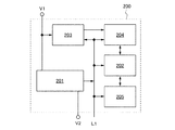
図1に示す電源制御回路201は、トランジスタ101、トランジスタ102、トランジスタ103、容量素子104、及び容量素子105を有する。また、プロセッサ202は、例えば、レジスタやキャッシュメモリ等の揮発性の記憶装置を一または複数有する。
A power
第1のスイッチング素子として機能するトランジスタ101のソース及びドレインの一方は、容量素子104の一対の電極のうちの一方と、プロセッサ202と、電気的に接続され、ノードN1を構成し、ソース及びドレインの他方は、第1の電位が与えられる第1の電源線V1と電気的に接続される。また、容量素子104の一対の電極のうち他方は、第1の電位よりも低い第2の電位が与えられる第2の電源線V2と電気的に接続されている。
One of a source and a drain of the
第2のスイッチング素子として機能するトランジスタ102のソース及びドレインの一方は、第3のスイッチング素子として機能するトランジスタ103のソース及びドレインの一方と、トランジスタ101のゲートと電気的に接続され、ノードN2を構成している。トランジスタ102のソース及びドレインの他方は、第1の電源線V1と電気的に接続されている。また、トランジスタ103のソース及びドレインの他方は、第2の電源線V2と電気的に接続されている。
One of a source and a drain of the
トランジスタ102のゲートは、制御信号S1が入力される信号線と、容量素子105の一対の電極のうちの一方とが電気的に接続されてノードN3を構成する。容量素子105をトランジスタ102のゲートに電気的に接続することにより、制御信号S1が入力される信号線からの電位の供給が停止しても、一定期間オンを保つことができる。また、トランジスタ103のゲートは、制御信号S2が入力される信号線と、電気的に接続される。容量素子105の一対の電極のうち他方は、第2の電源線V2と電気的に接続される。
A gate of the
トランジスタ101は、ノードN2の電位に基づいてオン状態またはオフ状態が制御され、トランジスタ102は、制御信号S1に基づいてオン状態またはオフ状態が制御され、トランジスタ103は、制御信号S2に基づいてオン状態またはオフ状態が制御される。
The
トランジスタ101は、オフ電流が小さいトランジスタを用いることが好ましい。オフ電流が小さいトランジスタとして、例えば、シリコンよりもバンドギャップが広く、真性キャリア密度がシリコンよりも低い半導体にチャネルが形成されるトランジスタであることが好ましい。このような半導体としては、例えば、シリコンの2倍以上のバンドギャップを有することが好ましく、例えば、酸化ガリウムなどの酸化物半導体、窒化ガリウムなどの窒化物半導体、炭化シリコン、ガリウムヒ素などの化合物半導体が挙げられる。
As the
トランジスタ101に用いる半導体は、電子供与体(ドナー)となる水または水素などの不純物が低減され、なおかつ酸素欠損が低減されることにより、高純度化された酸化物半導体(purified Oxide Semiconductor)であることが好ましい。高純度化された酸化物半導体は、i型(真性半導体)又はi型に限りなく近い。そのため、上記酸化物半導体を用いたトランジスタは、オフ電流が著しく小さいという特性を有する。また、酸化物半導体のバンドギャップは、2eV以上、好ましくは、2.5eV以上、より好ましくは3.0eV以上である。さらに、水または水素などの不純物濃度が十分に低減され、なおかつ酸素欠損が低減されることにより、高純度化された酸化物半導体を用いることにより、トランジスタのオフ電流を著しく小さくすることができる。
A semiconductor used for the
具体的に、高純度化された酸化物半導体膜を用いたトランジスタのオフ電流が小さいことは、いろいろな実験により証明できる。例えば、チャネル幅が1×106μmでチャネル長が10μmの素子であっても、ソースとドレイン間の電圧(ドレイン電圧)が1Vから10Vの範囲において、オフ電流が、半導体パラメータアナライザの測定限界以下、すなわち1×10⁻¹³A以下という特性を得ることができる。この場合、オフ電流をトランジスタのチャネル幅で除した数値に相当するオフ電流密度は、100zA/μm以下であることが分かる。また、容量素子とトランジスタとを接続して、容量素子に流入または容量素子から流出する電荷を当該トランジスタで制御する回路を用いて、オフ電流密度の測定を行った。当該測定では、上記トランジスタに高純度化された酸化物半導体膜をチャネル形成領域に用い、容量素子の単位時間あたりの電荷量の推移から当該トランジスタのオフ電流密度を測定した。その結果、トランジスタのソースとドレイン間の電圧が3Vの場合に、数十yA/μmという、さらに低いオフ電流密度が得られることが分かった。従って、高純度化された酸化物半導体膜をチャネル形成領域に用いたトランジスタは、シリコンを用いたトランジスタに比べてオフ電流が著しく小さいといえる。 Specifically, the low off-state current of a transistor including a highly purified oxide semiconductor film can be proved by various experiments. For example, even if the device has a channel width of 1 × 10 6 μm and a channel length of 10 μm, the off-current is the measurement limit of the semiconductor parameter analyzer when the voltage between the source and drain (drain voltage) is in the range of 1V to 10V. The following characteristics can be obtained, that is, 1 × 10 −13 A or less. In this case, it can be seen that the off-current density corresponding to a value obtained by dividing the off-current by the channel width of the transistor is 100 zA / μm or less. Further, off-state current density was measured using a circuit in which a capacitor and a transistor are connected and charge flowing into or out of the capacitor is controlled by the transistor. In this measurement, a highly purified oxide semiconductor film of the transistor was used for a channel formation region, and the off-state current density of the transistor was measured from the change in charge amount per unit time of the capacitor. As a result, it was found that when the voltage between the source and drain of the transistor is 3 V, an even lower off-current density of several tens of yA / μm can be obtained. Therefore, a transistor using a highly purified oxide semiconductor film for a channel formation region can be said to have significantly smaller off-state current than a transistor using silicon.
トランジスタ101として、酸化物半導体膜にチャネルが形成されるトランジスタを用いることにより、ノードN1の電位が一定に保たれた後、トランジスタ101をオフ状態としても、トランジスタ101を介してリークする電荷量を著しく小さくすることができる。よって、ノードN1に電位を保持した後、トランジスタ101をオフ状態とすることにより、ノードN1の電位を長期間にわたり保持することができる。
By using a transistor in which a channel is formed in the oxide semiconductor film as the
また、トランジスタ102及びトランジスタ103として、酸化物半導体膜にチャネルが形成されるトランジスタを用いることにより、ノードN2の電位が一定に保たれた後、トランジスタ102又はトランジスタ103をオフ状態としても、トランジスタ102またはトランジスタ103を介してリークする電荷量を著しく小さくすることができる。よって、ノードN2の電位を保持した後、トランジスタ102またはトランジスタ103をオフ状態とすることにより、電源制御回路201で消費される電力を低減することができる。
Further, by using a transistor in which a channel is formed in the oxide semiconductor film as the
なお、トランジスタ102及びトランジスタ103は、酸化物半導体以外の半導体でなる層または基板にチャネルが形成されるトランジスタとすることもできる。例えば、シリコン層またはシリコン基板にチャネルが形成されるトランジスタとすることができる。
Note that the
なお、トランジスタ101〜トランジスタ103は、酸化物半導体層を挟んで上下に2つのゲートを有していてもよい。一方のゲートには、トランジスタのオン状態またはオフ状態を制御するための制御信号が与えられ、他方のゲートは、電気的に絶縁しているフローティングの状態であってもよいし、電位が他から与えられている状態であってもよい。後者の場合、一対のゲートに、同じ高さの電位が与えられていてもよいし、他方のゲートにのみ接地電位などの固定電位が与えられていてもよい。他方のゲートに与える電位の高さを制御することで、トランジスタのしきい値電圧を制御することができる。
Note that the
(電源制御回路の動作)
次に、プロセッサ202へ電源の供給の後、消費電力を削減するために電源の供給を停止し、再び電源を供給する場合の電源制御回路201の駆動方法について、図2を参照して説明する。
(Operation of power control circuit)
Next, a driving method of the power
(通常動作)
図2(A)に示す通常動作について説明する。図2(A)は、プロセッサ202に、電源(第1の電源線V1としてハイレベル電位)が与えられている状態を示している。トランジスタ102のゲートに、制御信号S1としてハイレベル電位が与えられることにより、トランジスタ102はオン状態となる。また、トランジスタ103のゲートに、制御信号S2としてローレベル電位が与えられることにより、トランジスタ103はオフ状態となる。よって、ノードN2の電位はハイレベル電位となり、トランジスタ101のゲートにハイレベル電位が与えられるため、トランジスタ101はオン状態となる。こうして、プロセッサ202に第1の電源線V1のハイレベル電位が与えられる。
(Normal operation)
A normal operation illustrated in FIG. 2A will be described. FIG. 2A shows a state where power is supplied to the processor 202 (high-level potential as the first power supply line V1). By applying a high-level potential as the control signal S1 to the gate of the
(回路ブロックへ電源供給停止動作)
図2(B)に示すプロセッサ202へ電源の供給を停止する動作について説明する。トランジスタ102のゲートに、制御信号S1としてローレベル電位が与えられることにより、トランジスタ102はオフ状態となる。また、トランジスタ103のゲートに、制御信号S2としてハイレベル電位が与えられることにより、トランジスタ103はオン状態となる。よって、ノードN2の電位はローレベル電位となり、トランジスタ101のゲートにローレベル電位が与えられるため、トランジスタ101はオフ状態となる。
(Operation to stop power supply to the circuit block)
An operation for stopping the supply of power to the
本実施の形態に示す電源制御回路201では、トランジスタ101として、オフ電流が極めて小さいトランジスタを用いている。そのため、トランジスタ101をオフ状態とすることにより、第1の電源線V1から、プロセッサ202へ流れる電流を遮断することができる。これにより、プロセッサ202で消費される電力を削減することができる。このように、電源制御回路201は、パワーゲーティング用のスイッチとして機能させることができる。
In the power
(通常動作再開)
また、プロセッサ202において、通常動作を再開する際には、図2(A)に示すように、トランジスタ102のゲートに、制御信号S1としてハイレベル電位を与えることにより、トランジスタ102をオン状態とする。また、トランジスタ103のゲートに、制御信号S2としてローレベル電位を与えることにより、トランジスタ103をオフ状態とする。よって、ノードN3の電位はハイレベル電位となり、トランジスタ101のゲートにハイレベル電位が与えられるため、トランジスタ101はオン状態となる。こうして、プロセッサ202に第1の電源線V1のハイレベル電位が与えられ、通常動作が再開される。
(Resume normal operation)
When the
本実施の形態は、他の実施の形態と適宜組み合わせて実施することが可能である。 This embodiment can be implemented in appropriate combination with any of the other embodiments.
(実施の形態2)
本実施の形態では、プロセッサ202へ電源を供給した後、突然、電源の供給が停止した場合の信号処理回路200の駆動方法について、図3乃至図6を参照して説明する。
(Embodiment 2)
In this embodiment, a driving method of the
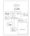
図3に、電源制御回路201を含む信号処理回路200のブロック図を示す。信号処理回路200は、電源制御回路201と、プロセッサ202と、検知回路203と、プロセッサ204と、不揮発性の記憶装置205と、を有する。ここで、プロセッサ202は、信号処理回路200を含む電子機器の動作を制御するためのメインのプロセッサであり、プロセッサ204は、電子機器への電源の供給が停止した場合に動作するサブのプロセッサである。また、検知回路203、プロセッサ204、記憶装置205、及びプロセッサ202は、それぞれL1などの配線によって接続される。
FIG. 3 shows a block diagram of the
プロセッサ202は、キャッシュメモリ、レジスタ等の揮発性の記憶装置を一又は複数有する。
The
記憶装置205は、ROM、EEPROM、フラッシュメモリ、磁気ディスク、光ディスク等の不揮発性の記憶装置を一又は複数有する。記憶装置205には、メインのプロセッサ202を動作させるためのプログラムや、サブのプロセッサ204を動作させるためのプログラムが格納されている。また、メインのプロセッサ202及びサブのプロセッサ204がプログラムを実行する際、各種データを一時的に格納するワークメモリとして使用される。また、メインのプロセッサ202の動作中に、突然、電源の供給が停止した場合、プロセッサ202に保持されているデータを保存するためのメモリとして使用される。
The
検知回路203は、第1の電源線V1に電気的に接続される。検知回路203は、第1の電源線V1の電位が、ハイレベル電位、ローレベル電位のいずれであるかを検知する。また、検知回路203は、検知された電位に基づき生成される第1の検知信号S3または第2の検知信号S4を、サブのプロセッサ204に送信する。検知回路203は、第1の電源線V1の電位がハイレベル電位からローレベル電位に変化したことを検知した場合は、第1の検知信号S3を、プロセッサ204に送信する。また、検知回路203は、第1の電源線V1の電位がローレベル電位からハイレベル電位に変化したことを検知した場合は、第2の検知信号S4を、プロセッサ204に送信する。
The
プロセッサ204は、プロセッサ202の動作とは独立して動作する。また、プロセッサ204は、電源の供給が停止した場合であっても動作することができる。プロセッサ204は、検知回路203から送信された第1の検知信号S3を受信すると、メインのプロセッサ202内に保持されたデータを、記憶装置205にバックアップするように、プロセッサ202にバックアップ指令を出す。また、検知回路203から送信された第2の検知信号S4を受信すると、記憶装置205に保持されたデータを、プロセッサ202にロードするように、プロセッサ202及び記憶装置205にロード指令を出す。
The
電源制御回路201は、実施の形態1に示す電源制御回路を適用することができる。
As the power
(信号処理回路200の動作方法)
次に、信号処理回路200の動作方法について、図4乃至図5を参照して説明する。
(Operation method of signal processing circuit 200)
Next, an operation method of the
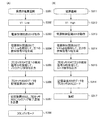
(突然の電源供給停止)
図4(A)に示すフローチャートのように、信号処理回路200に供給されていた電源が、突然、遮断される(ステップS301)。これにより、第1の電源線V1の第1の電位がハイレベル電位からローレベル電位となる(ステップS302)。そして、電源制御回路201が動作する(ステップS303)。
(Sudden power supply stop)
As in the flowchart shown in FIG. 4A, the power supplied to the
図5(A1)に、突然、電源の供給が停止した瞬間の電源制御回路201を示す。突然、電源の供給が停止すると、トランジスタ102のゲートに与えられていたハイレベル電位がローレベル電位となり、トランジスタ102がオフ状態となる。このとき、ノードN2に、電荷が残ったままトランジスタ102がオフ状態になってしまうと、トランジスタ101を完全にオフ状態にすることができなくなってしまう。
FIG. 5A1 illustrates the power
図5(A2)に、トランジスタ101の電気的特性を示すグラフを示す。例えば、ノードN2に、電荷が残っている場合、トランジスタ101のゲートには、正の電位であるVgaが与えられてしまい、トランジスタ101をオフ状態とすることができなくなる。これにより、トランジスタ101には、リーク電流が流れてしまい、ノードN1の電位も変動してしまうため、プロセッサ202は、動作を維持できなくなってしまう。
FIG. 5A2 is a graph illustrating the electrical characteristics of the
しかしながら、図5(B)に示すように、トランジスタ102のゲートには、容量素子105の一対の電極のうち一方が接続されたノードN3によって、電位が保持されている。これにより、トランジスタ102のゲートには、正の電位が与えられ続けるため、トランジスタ102がオフ状態となる時間を遅延させることができる。トランジスタ102がオフ状態となるまでの間に、ノードN2に残った電荷を第1の電源線V1へと移動させることにより、ノードN2の電位をローレベル電位とする。これにより、トランジスタ101をオフ状態とすることができる。
However, as illustrated in FIG. 5B, a potential is held at the gate of the
トランジスタ101として、酸化物半導体膜にチャネルが形成されるトランジスタを用いている。当該トランジスタは、オフ電流が著しく小さいため、容量素子104によって保持されたノードN1の電位を長期間保持することができる。よって、ノードN1の電位の変動を抑制することができる。
As the
そして、ノードN1には、電源供給時の電位であるハイレベル電位が保持されているため、プロセッサ202には、電力が供給され続ける(図5(C)参照)。 Since the node N1 holds a high-level potential which is a potential at the time of power supply, power is continuously supplied to the processor 202 (see FIG. 5C).
また、第1の電源線V1の電位がハイレベル電位からローレベル電位になると、検知回路203で、電位の変化が検知される。なお、ノードN1としてハイレベル電位が保持されることにより、配線L1もハイレベル電位が保たれている。よって、検知回路203は、配線L1から電源の供給を受けている。検知回路203で、電位の変化が検知されると、検知回路203では第1の検知信号S3を生成して、プロセッサ204に送信する(図4、ステップS304参照)。
Further, when the potential of the first power supply line V1 changes from the high level potential to the low level potential, the
プロセッサ204は、第1の検知信号S3を受信すると、プロセッサ202に保持されているデータを、記憶装置205に保持するようにプロセッサ202にバックアップ指令を出す(図4、ステップS305参照)。
Upon receiving the first detection signal S3, the
バックアップ指令を受けたプロセッサ202は、プロセッサ202から記憶装置205へデータを保存する(図4、ステップS306参照)。
Receiving the backup command, the
記憶装置205へデータが保存されたら、記憶装置205は、プロセッサ202に、バックアップ終了通知を送信(図4、ステップS307参照)することで、信号処理回路200は、スタンバイモードとなる(図4、ステップS308参照)。
When the data is stored in the
(電源復帰動作)
図4(B)に示すフローチャートのように、信号処理回路200への電源の供給が再開される(ステップS311参照)。これにより、第1の電源線V1の第1の電位がローレベル電位からハイレベル電位となる(ステップS312参照)。このとき、制御信号S1もローレベル電位からハイレベル電位となるため、トランジスタ102がオン状態となる。また、トランジスタ103のゲートには、制御信号S2として、ローレベル電位が与えられるため、トランジスタ103はオフ状態となる。よって、ノードN2の電位はハイレベル電位となり、トランジスタ101のゲートにはハイレベル電位が与えられるため、トランジスタ101はオン状態となる。こうして、プロセッサ202に第1の電源線V1のハイレベル電位が与えられる(ステップS313参照)。
(Power recovery operation)
As in the flowchart shown in FIG. 4B, the supply of power to the
また、第1の電源線V1の電位がローレベル電位からハイレベル電位になると、検知回路203で、電位の変化が検知される。検知回路203で、電位の変化が検知されると、検知回路203では第2の検知信号S4を生成して、プロセッサ204に送信する(ステップS314)。
Further, when the potential of the first power supply line V1 changes from the low level potential to the high level potential, the
プロセッサ204は、第2の検知信号S4を受信すると、記憶装置205に保持されているデータを、プロセッサ202にロードするように、プロセッサ202及び記憶装置205にロード指令を出す(ステップS315)。そして、記憶装置205のデータを、プロセッサ202にロードする(ステップS316)。
Upon receiving the second detection signal S4, the
こうして、信号処理回路200のデータの復帰が完了する(ステップS317)。
Thus, the data restoration of the
信号処理回路200において、電源制御回路201を設けることにより、信号処理回路200へ電源の供給が突然遮断された場合であっても、速やかに、プロセッサ202から記憶装置205へデータを退避させることができるため、プロセッサ202におけるデータの消失を防止することができる。
In the
また、パワーゲーティングを行っている最中に、突然、電源の供給が遮断された場合であっても、プロセッサ202に保持されたデータを速やかに記憶装置205へ退避させることができるため、プロセッサ202に保持されたデータの消滅を防止することができる。
In addition, even when power supply is suddenly interrupted during power gating, the data stored in the
例えば、電源制御回路201のトランジスタ101として、シリコンを用いたトランジスタを用いた場合では、オフ電流は1pAとなる。また、容量素子104の容量を例えば1pFとすると、ノードN1で電源電位(例えば、VDD)を変化量1mV未満で保持できる期間は1msecとなる。したがって、第1の電源線からの電源が突然遮断されてしまうと、プロセッサ202の動作は直ちに停止してしまうので、データは消滅してしまう。
For example, when a transistor using silicon is used as the
しかし、本発明の一態様では、電源制御回路201のトランジスタ101として、酸化物半導体を用いたトランジスタを用いているため、オフ電流を、100yAとすることができる。また、容量素子104の容量を例えば1pFとすると、ノードN1で電源電位を変化量1mV未満で保持できる期間は、107secとなる。したがって、この間に、プロセッサ202のデータを不揮発性の記憶装置205に保持することによって、突然電源の供給が停止した場合であってもプロセッサ202のデータの消滅を防止することができる。
However, in one embodiment of the present invention, a transistor including an oxide semiconductor is used as the
なお、実施の形態1に示す図1は、図3に示す信号処理回路200の一部を示している。したがって、図3に示す信号処理回路200において、プロセッサ202へ意図的に電源供給の遮断を行う場合には、実施の形態1に示すプロセッサ202へ電源供給停止動作を参照すればよい。
Note that FIG. 1 shown in
以上説明したように、電源制御回路201は、プロセッサ202への電源供給または遮断を意図的に行うのみならず、突然、電源供給が遮断された場合に、プロセッサ202のデータが消滅することを防止するために、電源の電位を保持することができる。電源制御回路201によって保持された電源の電位を利用して、プロセッサ202のデータを不揮発性の記憶装置205に退避させることで、プロセッサ202のデータが消滅することを防止することができる。このように、電源制御回路201は、パワーゲーティング用のスイッチ、及び電源供給が突然遮断されてしまった場合に、電源の電位を保持するための回路として機能させることができる。
As described above, the
(実施の形態3)
本実施の形態では、先の実施の形態に示す電源制御回路の断面の一部について、図6を参照して説明する。図6では、図3に示すプロセッサ202が有するトランジスタ510及び520上に、電源制御回路201が有するトランジスタ101及び容量素子104が、積層されている図を示す。
(Embodiment 3)
In this embodiment, part of a cross section of the power supply control circuit described in the above embodiment is described with reference to FIGS. 6 illustrates a diagram in which the
なお、上記トランジスタ101及びトランジスタ510は、nチャネル型トランジスタであり、トランジスタ520は、pチャネル型トランジスタである場合について説明する。
Note that the case where the
まず、下部に形成されたトランジスタ510及びトランジスタ520について説明する。
First, the
n型のトランジスタ510は、半導体材料を含む基板500に設けられたチャネル形成領域501と、チャネル形成領域501を挟むように設けられた低濃度不純物領域502及び高濃度不純物領域503(これらを合わせて単に不純物領域とも呼ぶ)と、該不純物領域に接して設けられた金属間化合物領域507と、チャネル形成領域501上に設けられたゲート絶縁層504aと、ゲート絶縁層504a上に設けられたゲート電極層505aと、金属間化合物領域507と接して設けられたソース電極層506a及びドレイン電極層506bと、を有する。ゲート電極層505aの側面には、側壁絶縁層508aが設けられている。トランジスタ510を覆うように絶縁層521及び絶縁層522が設けられている。絶縁層521及び絶縁層522に形成された開口を通じて、ソース電極層506a及びドレイン電極層506bと、金属間化合物領域507とが接続されている。
The n-
低濃度不純物領域502及び高濃度不純物領域503には、n型の導電型を付与する不純物が添加されている。n型を付与する不純物元素としては、リンやヒ素等を用いることができる。
An impurity imparting n-type conductivity is added to the low concentration impurity region 502 and the high
p型のトランジスタ520は、半導体材料を含む基板500に設けられたチャネル形成領域511と、チャネル形成領域511を挟むように設けられた低濃度不純物領域512及び高濃度不純物領域513(これらを合わせて単に不純物領域とも呼ぶ)と、該不純物領域に接して設けられた金属間化合物領域517と、チャネル形成領域511上に設けられたゲート絶縁層504bと、ゲート絶縁層504b上に設けられたゲート電極層505bと、金属間化合物領域517と接して設けられたソース電極層506c及びドレイン電極層506dと、を有する。ゲート電極層505bの側面には、側壁絶縁層508bが設けられている。トランジスタ520を覆うように絶縁層521及び絶縁層522が設けられている。絶縁層521及び絶縁層522に形成された開口を通じて、ソース電極層506c及びドレイン電極層506dと、金属間化合物領域517とが接続している。
A p-
低濃度不純物領域512及び高濃度不純物領域513には、p型の導電型を付与する不純物が添加されている。p型を付与する不純物元素として、硼素、アルミニウム、ガリウム等を用いることができる。
An impurity imparting p-type conductivity is added to the low
また、基板500には、トランジスタ510と、トランジスタ520のそれぞれを囲むように素子分離絶縁膜509が設けられている。
In addition, an element
基板500として、例えば、ガラス基板、セラミック基板、石英基板、サファイア基板等を用いることができる。また、シリコンや炭化シリコンなどの単結晶半導体基板や、多結晶半導体基板、GaAs基板、InP基板、GaN基板、SiC基板、GaP基板、GaInAsP基板、ZnSe基板等の化合物半導体基板を用いることができる。
As the
図6では、トランジスタ510及びトランジスタ520が、半導体基板にチャネルが形成されるトランジスタである場合について示すが、トランジスタ510及びトランジスタ520が、絶縁表面上に形成された半導体膜にチャネルが形成されるトランジスタであってもよい。
FIG. 6 illustrates the case where the
半導体膜は、非晶質シリコン、多結晶シリコン、単結晶シリコンなどを用いて形成される。非晶質シリコンは、CVD法やスパッタリング法などにより成膜され、多結晶シリコンは、非晶質シリコンにレーザビームを照射することにより結晶化される。また、単結晶シリコンは、単結晶シリコン基板に水素イオンを注入して表層部を剥離することにより形成される。 The semiconductor film is formed using amorphous silicon, polycrystalline silicon, single crystal silicon, or the like. Amorphous silicon is formed by CVD, sputtering, or the like, and polycrystalline silicon is crystallized by irradiating the amorphous silicon with a laser beam. Single crystal silicon is formed by implanting hydrogen ions into a single crystal silicon substrate and peeling off the surface layer portion.
半導体基板として、単結晶半導体基板を用いることにより、トランジスタ510及びトランジスタ520を、高速動作させることができる。なお、図6に図示しないが、先の実施の形態に示すプロセッサ202、プロセッサ204、及び検知回路203も、単結晶半導体基板に形成されることが好ましい。
By using a single crystal semiconductor substrate as the semiconductor substrate, the
ゲート絶縁層504a、504b上に形成されたゲート電極層505a、505bの側面には、側壁絶縁層508a、508bが設けられている。基板500にn型の不純物を添加する際に、ゲート電極層505a及び側壁絶縁層508aをマスクとして用いることで、不純物濃度が異なる低濃度不純物領域502と、高濃度不純物領域503を、自己整合的に形成することができる。また、基板500にp型の不純物を添加する際に、ゲート電極層505b及び側壁絶縁層508bをそれぞれマスクとして用いることで、不純物濃度が異なる低濃度不純物領域512と、高濃度不純物領域513を、自己整合的に形成することができる。
Side
ゲート絶縁層504a及びゲート絶縁層504bは、CVD法、スパッタリング法、熱酸化法などにより、酸化シリコン、酸化窒化シリコン、窒化シリコン、窒化酸化シリコン等を用いて形成される。
The
ゲート電極層505a、505bは、スパッタリング法やCVD法により、モリブデン、チタン、タンタル、タングステン、アルミニウム、銅、クロム、ネオジム、スカンジウム等の金属材料、またはこれらを主成分とする合金材料を用いて形成される。
The
側壁絶縁層508a、508bは、CVD法、スパッタリング法により、酸化シリコン、酸化窒化シリコン、窒化シリコン、窒化酸化シリコン等を用いて形成される。図6では、側壁絶縁層508a、508bは、積層構造で形成されている場合について示す。
The
絶縁層521及び絶縁層522は、CVD法、スパッタリング法等により、酸化シリコン、酸化窒化シリコン、窒化酸化シリコン等を用いて形成される。また、低温酸化(LTO:Low Temperature Oxidation)法により形成された酸化シリコンを用いてもよい。また、TEOS(Tetraethyl−Ortho−Silicate)若しくはシラン等と、酸素若しくは亜酸化窒素等とを反応させて形成した段差被覆性のよい酸化シリコンを用いてもよい。なお、絶縁層522は、その表面の平坦性を高めるために研磨処理(例えば、化学的機械研磨(Chemical Mechanical Polishing:CMP)法)、ドライエッチング処理、プラズマ処理が行われることが好ましい。
The insulating
ソース電極層506a、ドレイン電極層506b、ソース電極層506c、及びドレイン電極層506dは、スパッタリング法やPECVD法により、モリブデン、チタン、タンタル、タングステン、アルミニウム、銅、クロム、ネオジム、スカンジウム等の金属材料、またはこれらを主成分とする合金材料を用いて形成される。
The
絶縁層522上には、配線層523a〜523cが形成されている。配線層523a〜523cは、ソース電極層506aなどの記載を参酌できる。
On the insulating
配線層523a〜523c上に、絶縁層524が形成されている。絶縁層524は、絶縁層521などの記載を参酌できる。
An insulating
絶縁層524上には、電極層525が形成されている。電極層525は、トランジスタ101のゲートとして機能する。電極層525は、ソース電極層506aなどの記載を参酌できる。
An
電極層525に絶縁層526が接して設けられている。絶縁層526は、電極層525上に絶縁膜を形成した後、電極層525の上面が露出するまで、CMP法などの研磨処理、ドライエッチング処理、プラズマ処理を行うことで形成される。
An insulating
電極層525及び絶縁層526上に、絶縁層527、絶縁層528、絶縁層529が形成されている。絶縁層526〜529は、絶縁層521、522と同様の方法により、同様の材料を用いて形成される。本実施の形態では、電極層525、絶縁層526上に、3層の絶縁層を形成する例について示しているが、1層または2層であってもよいし、4層以上であってもよい。
An insulating
絶縁層529上には、酸化物半導体層530が設けられている。
An
酸化物半導体層530は、少なくともインジウム(In)あるいは亜鉛(Zn)を含むことが好ましい。また、該酸化物半導体層を用いたトランジスタの電気的特性のばらつきを減らすためのスタビライザーとして、それらに加えてガリウム(Ga)、スズ(Sn)、ハフニウム(Hf)、アルミニウム(Al)、ジルコニウム(Zr)のいずれか一または複数を含むことが好ましい。
The
また、他のスタビライザーとして、ランタノイドである、ランタン(La)、セリウム(Ce)、プラセオジム(Pr)、ネオジム(Nd)、サマリウム(Sm)、ユウロピウム(Eu)、ガドリニウム(Gd)、テルビウム(Tb)、ジスプロシウム(Dy)、ホルミウム(Ho)、エルビウム(Er)、ツリウム(Tm)、イッテルビウム(Yb)、ルテチウム(Lu)のいずれか一種または複数種を含んでいてもよい。 As other stabilizers, lanthanoids such as lanthanum (La), cerium (Ce), praseodymium (Pr), neodymium (Nd), samarium (Sm), europium (Eu), gadolinium (Gd), terbium (Tb) , Dysprosium (Dy), holmium (Ho), erbium (Er), thulium (Tm), ytterbium (Yb), or lutetium (Lu) may be included.
例えば、酸化物半導体として、酸化インジウム、酸化ガリウム、酸化スズ、酸化亜鉛、二元系金属の酸化物であるIn−Zn系酸化物、Sn−Zn系酸化物、Al−Zn系酸化物、Zn−Mg系酸化物、Sn−Mg系酸化物、In−Mg系酸化物、In−Ga系酸化物、三元系金属の酸化物であるIn−Ga−Zn系酸化物(IGZOとも表記する)、In−Al−Zn系酸化物、In−Sn−Zn系酸化物、Sn−Ga−Zn系酸化物、Al−Ga−Zn系酸化物、Sn−Al−Zn系酸化物、In−Hf−Zn系酸化物、In−La−Zn系酸化物、In−Pr−Zn系酸化物、In−Nd−Zn系酸化物、In−Sm−Zn系酸化物、In−Eu−Zn系酸化物、In−Gd−Zn系酸化物、In−Tb−Zn系酸化物、In−Dy−Zn系酸化物、In−Ho−Zn系酸化物、In−Er−Zn系酸化物、In−Tm−Zn系酸化物、In−Yb−Zn系酸化物、In−Lu−Zn系酸化物、四元系金属の酸化物であるIn−Sn−Ga−Zn系酸化物、In−Hf−Ga−Zn系酸化物、In−Al−Ga−Zn系酸化物、In−Sn−Al−Zn系酸化物、In−Sn−Hf−Zn系酸化物、In−Hf−Al−Zn系酸化物を用いることができる。 For example, as an oxide semiconductor, indium oxide, gallium oxide, tin oxide, zinc oxide, binary metal oxides such as In—Zn oxide, Sn—Zn oxide, Al—Zn oxide, Zn -Mg-based oxide, Sn-Mg-based oxide, In-Mg-based oxide, In-Ga-based oxide, In-Ga-Zn-based oxide which is an oxide of a ternary metal (also referred to as IGZO) In-Al-Zn-based oxide, In-Sn-Zn-based oxide, Sn-Ga-Zn-based oxide, Al-Ga-Zn-based oxide, Sn-Al-Zn-based oxide, In-Hf- Zn-based oxide, In-La-Zn-based oxide, In-Pr-Zn-based oxide, In-Nd-Zn-based oxide, In-Sm-Zn-based oxide, In-Eu-Zn-based oxide, In-Gd-Zn-based oxide, In-Tb-Zn-based oxide, In-Dy- n-based oxide, In-Ho-Zn-based oxide, In-Er-Zn-based oxide, In-Tm-Zn-based oxide, In-Yb-Zn-based oxide, In-Lu-Zn-based oxide, In-Sn-Ga-Zn-based oxides, In-Hf-Ga-Zn-based oxides, In-Al-Ga-Zn-based oxides, In-Sn-Al-Zn-based oxides that are quaternary metal oxides An oxide, an In—Sn—Hf—Zn-based oxide, or an In—Hf—Al—Zn-based oxide can be used.
なお、例えば、In−Ga−Zn系酸化物とは、InとGaとZnを含む酸化物という意味であり、InとGaとZnの比率は問わない。また、InとGaとZn以外の金属元素を含んでいてもよい。当該In−Ga−Zn系酸化物を用いたトランジスタは、無電界時の抵抗が十分に高くオフ電流を十分に小さくすることが可能であり、また、移動度も高い。 Note that for example, an In—Ga—Zn-based oxide means an oxide containing In, Ga, and Zn, and there is no limitation on the ratio of In, Ga, and Zn. Moreover, metal elements other than In, Ga, and Zn may be included. A transistor using the In—Ga—Zn-based oxide has sufficiently high resistance when no electric field is applied, can sufficiently reduce off-state current, and has high mobility.
例えば、In:Ga:Zn=1:1:1(=1/3:1/3:1/3)あるいはIn:Ga:Zn=2:2:1(=2/5:2/5:1/5)の原子比のIn−Ga−Zn系酸化物やその組成の近傍の酸化物を用いることができる。あるいは、In:Sn:Zn=1:1:1(=1/3:1/3:1/3)、In:Sn:Zn=2:1:3(=1/3:1/6:1/2)あるいはIn:Sn:Zn=2:1:5(=1/4:1/8:5/8)の原子比のIn−Sn−Zn系酸化物やその組成の近傍の酸化物を用いるとよい。 For example, In: Ga: Zn = 1: 1: 1 (= 1/3: 1/3: 1/3) or In: Ga: Zn = 2: 2: 1 (= 2/5: 2/5: 1). / 5) atomic ratio In—Ga—Zn-based oxides and oxides in the vicinity of the composition can be used. Alternatively, In: Sn: Zn = 1: 1: 1 (= 1/3: 1/3: 1/3), In: Sn: Zn = 2: 1: 3 (= 1/3: 1/6: 1) / 2) or In: Sn: Zn = 2: 1: 5 (= 1/4: 1/8: 5/8) atomic ratio In—Sn—Zn-based oxide or an oxide in the vicinity of the composition. Use it.
例えば、In−Sn−Zn系酸化物では比較的容易に高い移動度が得られる。しかしながら、In−Ga−Zn系酸化物でも、バルク内欠陥密度を低減することにより移動度を上げることができる。 For example, high mobility can be obtained relatively easily with an In—Sn—Zn-based oxide. However, mobility can be increased by reducing the defect density in the bulk also in the case of using an In—Ga—Zn-based oxide.
以下では、酸化物半導体膜の構造について説明する。 Hereinafter, the structure of the oxide semiconductor film is described.
酸化物半導体膜は、非単結晶酸化物半導体膜と単結晶酸化物半導体膜とに大別される。非単結晶酸化物半導体膜とは、CAAC−OS(C Axis Aligned Crystalline Oxide Semiconductor)膜、多結晶酸化物半導体膜、微結晶酸化物半導体膜、非晶質酸化物半導体膜などをいう。 An oxide semiconductor film is roughly classified into a non-single-crystal oxide semiconductor film and a single-crystal oxide semiconductor film. The non-single-crystal oxide semiconductor film refers to a CAAC-OS (C Axis Crystalline Oxide Semiconductor) film, a polycrystalline oxide semiconductor film, a microcrystalline oxide semiconductor film, an amorphous oxide semiconductor film, or the like.
まずは、CAAC−OS膜について説明する。 First, the CAAC-OS film is described.
CAAC−OS膜は、複数の結晶部を有する酸化物半導体膜の一つであり、ほとんどの結晶部は、一辺が100nm未満の立方体内に収まる大きさである。従って、CAAC−OS膜に含まれる結晶部は、一辺が10nm未満、5nm未満または3nm未満の立方体内に収まる大きさの場合も含まれる。 The CAAC-OS film is one of oxide semiconductor films having a plurality of crystal parts, and most of the crystal parts are large enough to fit in a cube whose one side is less than 100 nm. Therefore, the case where a crystal part included in the CAAC-OS film fits in a cube whose one side is less than 10 nm, less than 5 nm, or less than 3 nm is included.
CAAC−OS膜を透過型電子顕微鏡(TEM:Transmission Electron Microscope)によって観察すると、明確な結晶部同士の境界、即ち結晶粒界(グレインバウンダリーともいう。)を確認することができない。そのため、CAAC−OS膜は、結晶粒界に起因する電子移動度の低下が起こりにくいといえる。 When the CAAC-OS film is observed with a transmission electron microscope (TEM), a clear boundary between crystal parts, that is, a grain boundary (also referred to as a grain boundary) cannot be confirmed. Therefore, it can be said that the CAAC-OS film is unlikely to decrease in electron mobility due to crystal grain boundaries.
CAAC−OS膜を、試料面と概略平行な方向からTEMによって観察(断面TEM観察)すると、結晶部において、金属原子が層状に配列していることを確認できる。金属原子の各層は、CAAC−OS膜の膜を形成する面(被形成面ともいう。)または上面の凹凸を反映した形状であり、CAAC−OS膜の被形成面または上面と平行に配列する。 When the CAAC-OS film is observed by TEM (cross-sectional TEM observation) from a direction substantially parallel to the sample surface, it can be confirmed that metal atoms are arranged in layers in the crystal part. Each layer of metal atoms has a shape reflecting unevenness of a surface (also referred to as a formation surface) or an upper surface on which the CAAC-OS film is formed, and is arranged in parallel with the formation surface or the upper surface of the CAAC-OS film. .
一方、CAAC−OS膜を、試料面と概略垂直な方向からTEMによって観察(平面TEM観察)すると、結晶部において、金属原子が三角形状または六角形状に配列していることを確認できる。しかしながら、異なる結晶部間で、金属原子の配列に規則性は見られない。 On the other hand, when the CAAC-OS film is observed by TEM (planar TEM observation) from a direction substantially perpendicular to the sample surface, it can be confirmed that metal atoms are arranged in a triangular shape or a hexagonal shape in the crystal part. However, there is no regularity in the arrangement of metal atoms between different crystal parts.
断面TEM観察および平面TEM観察より、CAAC−OS膜の結晶部は配向性を有していることがわかる。 From the cross-sectional TEM observation and the planar TEM observation, it is found that the crystal part of the CAAC-OS film has orientation.
CAAC−OS膜に対し、X線回折(XRD:X−Ray Diffraction)装置を用いて構造解析を行うと、例えばInGaZnO4の結晶を有するCAAC−OS膜のout−of−plane法による解析では、回折角(2θ)が31°近傍にピークが現れる場合がある。このピークは、InGaZnO4の結晶の(009)面に帰属されることから、CAAC−OS膜の結晶がc軸配向性を有し、c軸が被形成面または上面に概略垂直な方向を向いていることが確認できる。 When structural analysis is performed on a CAAC-OS film using an X-ray diffraction (XRD) apparatus, for example, in the analysis of a CAAC-OS film having an InGaZnO 4 crystal by an out-of-plane method, A peak may appear when the diffraction angle (2θ) is around 31 °. Since this peak is attributed to the (009) plane of the InGaZnO 4 crystal, the CAAC-OS film crystal has c-axis orientation, and the c-axis is in a direction substantially perpendicular to the formation surface or the top surface. Can be confirmed.
一方、CAAC−OS膜に対し、c軸に概略垂直な方向からX線を入射させるin−plane法による解析では、2θが56°近傍にピークが現れる場合がある。このピークは、InGaZnO4の結晶の(110)面に帰属される。InGaZnO4の単結晶酸化物半導体膜であれば、2θを56°近傍に固定し、試料面の法線ベクトルを軸(φ軸)として試料を回転させながら分析(φスキャン)を行うと、(110)面と等価な結晶面に帰属されるピークが6本観察される。これに対し、CAAC−OS膜の場合は、2θを56°近傍に固定してφスキャンした場合でも、明瞭なピークが現れない。 On the other hand, when the CAAC-OS film is analyzed by an in-plane method in which X-rays are incident from a direction substantially perpendicular to the c-axis, a peak may appear when 2θ is around 56 °. This peak is attributed to the (110) plane of the InGaZnO 4 crystal. In the case of a single crystal oxide semiconductor film of InGaZnO 4 , when 2θ is fixed in the vicinity of 56 ° and analysis (φ scan) is performed while rotating the sample with the normal vector of the sample surface as the axis (φ axis), Six peaks attributed to the crystal plane equivalent to the (110) plane are observed. On the other hand, in the case of a CAAC-OS film, a peak is not clearly observed even when φ scan is performed with 2θ fixed at around 56 °.
以上のことから、CAAC−OS膜では、異なる結晶部間ではa軸およびb軸の配向は不規則であるが、c軸配向性を有し、かつc軸が被形成面または上面の法線ベクトルに平行な方向を向いていることがわかる。従って、前述の断面TEM観察で確認された層状に配列した金属原子の各層は、結晶のab面に平行な面である。 From the above, in the CAAC-OS film, the orientation of the a-axis and the b-axis is irregular between different crystal parts, but the c-axis is aligned, and the c-axis is a normal line of the formation surface or the top surface. It can be seen that the direction is parallel to the vector. Therefore, each layer of metal atoms arranged in a layer shape confirmed by the above-mentioned cross-sectional TEM observation is a plane parallel to the ab plane of the crystal.
なお、結晶部は、CAAC−OS膜を成膜した際、または加熱処理などの結晶化処理を行った際に形成される。上述したように、結晶のc軸は、CAAC−OS膜の被形成面または上面の法線ベクトルに平行な方向に配向する。従って、例えば、CAAC−OS膜の形状をエッチングなどによって変化させた場合、結晶のc軸がCAAC−OS膜の被形成面または上面の法線ベクトルと平行にならないこともある。 Note that the crystal part is formed when a CAAC-OS film is formed or when crystallization treatment such as heat treatment is performed. As described above, the c-axis of the crystal is oriented in a direction parallel to the normal vector of the formation surface or the top surface of the CAAC-OS film. Therefore, for example, when the shape of the CAAC-OS film is changed by etching or the like, the c-axis of the crystal may not be parallel to the normal vector of the formation surface or the top surface of the CAAC-OS film.
また、CAAC−OS膜中の結晶化度が均一でなくてもよい。例えば、CAAC−OS膜の結晶部が、CAAC−OS膜の上面近傍からの結晶成長によって形成される場合、上面近傍の領域は、被形成面近傍の領域よりも結晶化度が高くなることがある。また、CAAC−OS膜に不純物を添加する場合、不純物が添加された領域の結晶化度が変化し、部分的に結晶化度の異なる領域が形成されることもある。 Further, the crystallinity in the CAAC-OS film is not necessarily uniform. For example, in the case where the crystal part of the CAAC-OS film is formed by crystal growth from the vicinity of the top surface of the CAAC-OS film, the region near the top surface can have a higher degree of crystallinity than the region near the formation surface. is there. In addition, in the case where an impurity is added to the CAAC-OS film, the crystallinity of a region to which the impurity is added changes, and a region having a different degree of crystallinity may be formed.
なお、InGaZnO4の結晶を有するCAAC−OS膜のout−of−plane法による解析では、2θが31°近傍のピークの他に、2θが36°近傍にもピークが現れる場合がある。2θが36°近傍のピークは、CAAC−OS膜中の一部に、c軸配向性を有さない結晶が含まれることを示している。CAAC−OS膜は、2θが31°近傍にピークを示し、2θが36°近傍にピークを示さないことが好ましい。 Note that when the CAAC-OS film including an InGaZnO 4 crystal is analyzed by an out-of-plane method, a peak may also appear when 2θ is around 36 ° in addition to the peak where 2θ is around 31 °. A peak at 2θ of around 36 ° indicates that a crystal having no c-axis alignment is included in part of the CAAC-OS film. The CAAC-OS film preferably has a peak at 2θ of around 31 ° and no peak at 2θ of around 36 °.
CAAC−OS膜は、不純物濃度の低い酸化物半導体膜である。不純物は、水素、炭素、シリコン、遷移金属元素などの酸化物半導体膜の主成分以外の元素である。特に、シリコンなどの、酸化物半導体膜を構成する金属元素よりも酸素との結合力の強い元素は、酸化物半導体膜から酸素を奪うことで酸化物半導体膜の原子配列を乱し、結晶性を低下させる要因となる。また、鉄やニッケルなどの重金属、アルゴン、二酸化炭素などは、原子半径(または分子半径)が大きいため、酸化物半導体膜内部に含まれると、酸化物半導体膜の原子配列を乱し、結晶性を低下させる要因となる。なお、酸化物半導体膜に含まれる不純物は、キャリアトラップやキャリア発生源となる場合がある。 The CAAC-OS film is an oxide semiconductor film with a low impurity concentration. The impurity is an element other than the main component of the oxide semiconductor film, such as hydrogen, carbon, silicon, or a transition metal element. In particular, an element such as silicon, which has a stronger bonding force with oxygen than the metal element included in the oxide semiconductor film, disturbs the atomic arrangement of the oxide semiconductor film by depriving the oxide semiconductor film of oxygen, and has crystallinity. It becomes a factor to reduce. In addition, heavy metals such as iron and nickel, argon, carbon dioxide, and the like have large atomic radii (or molecular radii). Therefore, if they are contained inside an oxide semiconductor film, the atomic arrangement of the oxide semiconductor film is disturbed, resulting in crystallinity. It becomes a factor to reduce. Note that the impurity contained in the oxide semiconductor film might serve as a carrier trap or a carrier generation source.
また、CAAC−OS膜は、欠陥準位密度の低い酸化物半導体膜である。例えば、酸化物半導体膜中の酸素欠損は、キャリアトラップとなることや、水素を捕獲することによってキャリア発生源となることがある。 The CAAC-OS film is an oxide semiconductor film with a low density of defect states. For example, oxygen vacancies in the oxide semiconductor film can serve as carrier traps or can generate carriers by capturing hydrogen.
不純物濃度が低く、欠陥準位密度が低い(酸素欠損の少ない)ことを、高純度真性または実質的に高純度真性と呼ぶ。高純度真性または実質的に高純度真性である酸化物半導体膜は、キャリア発生源が少ないため、キャリア密度を低くすることができる。従って、当該酸化物半導体膜を用いたトランジスタは、しきい値電圧がマイナスとなる電気特性(ノーマリーオンともいう。)になることが少ない。また、高純度真性または実質的に高純度真性である酸化物半導体膜は、キャリアトラップが少ない。そのため、当該酸化物半導体膜を用いたトランジスタは、電気特性の変動が小さく、信頼性の高いトランジスタとなる。なお、酸化物半導体膜のキャリアトラップに捕獲された電荷は、放出するまでに要する時間が長く、あたかも固定電荷のように振る舞うことがある。そのため、不純物濃度が高く、欠陥準位密度が高い酸化物半導体膜を用いたトランジスタは、電気特性が不安定となる場合がある。 A low impurity concentration and a low density of defect states (small number of oxygen vacancies) is called high purity intrinsic or substantially high purity intrinsic. A highly purified intrinsic or substantially highly purified intrinsic oxide semiconductor film has few carrier generation sources, and thus can have a low carrier density. Therefore, a transistor including the oxide semiconductor film rarely has electrical characteristics (also referred to as normally-on) in which the threshold voltage is negative. A highly purified intrinsic or substantially highly purified intrinsic oxide semiconductor film has few carrier traps. Therefore, a transistor including the oxide semiconductor film has a small change in electrical characteristics and has high reliability. Note that the charge trapped in the carrier trap of the oxide semiconductor film takes a long time to be released, and may behave as if it were a fixed charge. Therefore, a transistor including an oxide semiconductor film with a high impurity concentration and a high density of defect states may have unstable electrical characteristics.
また、CAAC−OS膜を用いたトランジスタは、可視光や紫外光の照射による電気特性の変動が小さい。 In addition, a transistor including a CAAC-OS film has little variation in electrical characteristics due to irradiation with visible light or ultraviolet light.
次に、微結晶酸化物半導体膜について説明する。 Next, a microcrystalline oxide semiconductor film is described.
微結晶酸化物半導体膜は、TEMによる観察像では、明確に結晶部を確認することができない場合がある。微結晶酸化物半導体膜に含まれる結晶部は、1nm以上100nm以下、または1nm以上10nm以下の大きさであることが多い。特に、1nm以上10nm以下、または1nm以上3nm以下の微結晶であるナノ結晶(nc:nanocrystal)を有する酸化物半導体膜を、nc−OS(nanocrystalline Oxide Semiconductor)膜と呼ぶ。また、nc−OS膜は、例えば、TEMによる観察像では、結晶粒界を明確に確認できない場合がある。 In the microcrystalline oxide semiconductor film, there is a case where a crystal part cannot be clearly confirmed in an observation image using a TEM. In most cases, a crystal part included in the microcrystalline oxide semiconductor film has a size of 1 nm to 100 nm, or 1 nm to 10 nm. In particular, an oxide semiconductor film including a nanocrystal (nc) that is a microcrystal of 1 nm to 10 nm, or 1 nm to 3 nm is referred to as an nc-OS (nanocrystalline Oxide Semiconductor) film. In the nc-OS film, for example, a crystal grain boundary may not be clearly confirmed in an observation image using a TEM.
nc−OS膜は、微小な領域(例えば、1nm以上10nm以下の領域、特に1nm以上3nm以下の領域)において原子配列に周期性を有する。また、nc−OS膜は、異なる結晶部間で結晶方位に規則性が見られない。そのため、膜全体で配向性が見られない。従って、nc−OS膜は、分析方法によっては、非晶質酸化物半導体膜と区別が付かない場合がある。例えば、nc−OS膜に対し、結晶部よりも大きい径のX線を用いるXRD装置を用いて構造解析を行うと、out−of−plane法による解析では、結晶面を示すピークが検出されない。また、nc−OS膜は、結晶部よりも大きいプローブ径(例えば50nm以上)の電子線を用いる電子線回折(制限視野電子線回折ともいう。)を行うと、ハローパターンのような回折像が観測される。一方、nc−OS膜は、結晶部の大きさと近いか結晶部より小さいプローブ径(例えば1nm以上30nm以下)の電子線を用いる電子線回折(ナノビーム電子線回折ともいう。)を行うと、スポットが観測される。また、nc−OS膜のナノビーム電子線回折を行うと、円を描くように(リング状に)輝度の高い領域が観測される場合がある。また、nc−OS膜のナノビーム電子線回折を行うと、リング状の領域内に複数のスポットが観測される場合がある。 The nc-OS film has periodicity in atomic arrangement in a very small region (eg, a region of 1 nm to 10 nm, particularly a region of 1 nm to 3 nm). In addition, the nc-OS film does not have regularity in crystal orientation between different crystal parts. Therefore, orientation is not seen in the whole film. Therefore, the nc-OS film may not be distinguished from an amorphous oxide semiconductor film depending on an analysis method. For example, when structural analysis is performed on the nc-OS film using an XRD apparatus using X-rays having a diameter larger than that of the crystal part, a peak indicating a crystal plane is not detected in the analysis by the out-of-plane method. Further, when nc-OS film is subjected to electron diffraction (also referred to as limited-field electron diffraction) using an electron beam with a probe diameter (for example, 50 nm or more) larger than that of a crystal part, a diffraction image like a halo pattern is obtained. Observed. On the other hand, when the nc-OS film is subjected to electron diffraction (also referred to as nanobeam electron diffraction) using an electron beam with a probe diameter (for example, 1 nm to 30 nm) that is close to the crystal part or smaller than the crystal part, Is observed. Further, when nanobeam electron diffraction of the nc-OS film is performed, a region with high luminance may be observed so as to draw a circle (in a ring shape). Further, when nanobeam electron diffraction is performed on the nc-OS film, a plurality of spots may be observed in the ring-shaped region.
nc−OS膜は、非晶質酸化物半導体膜よりも規則性の高い酸化物半導体膜である。そのため、nc−OS膜は、非晶質酸化物半導体膜よりも欠陥準位密度が低くなる。ただし、nc−OS膜は、異なる結晶部間で結晶方位に規則性が見られない。そのため、nc−OS膜は、CAAC−OS膜と比べて欠陥準位密度が高くなる。 The nc-OS film is an oxide semiconductor film that has higher regularity than an amorphous oxide semiconductor film. Therefore, the nc-OS film has a lower density of defect states than the amorphous oxide semiconductor film. Note that the nc-OS film does not have regularity in crystal orientation between different crystal parts. Therefore, the nc-OS film has a higher density of defect states than the CAAC-OS film.
なお、酸化物半導体膜は、例えば、非晶質酸化物半導体膜、微結晶酸化物半導体膜、CAAC−OS膜のうち、二種以上を有する積層膜であってもよい。 Note that the oxide semiconductor film may be a stacked film including two or more of an amorphous oxide semiconductor film, a microcrystalline oxide semiconductor film, and a CAAC-OS film, for example.
なお、非晶質酸化物半導体膜は、不純物が取り込まれやすくキャリア密度が高くなる傾向があるため、比較的容易に、比較的高い電界効果移動度を得ることができる。 Note that since an amorphous oxide semiconductor film tends to incorporate impurities and tends to have a high carrier density, a relatively high field-effect mobility can be obtained relatively easily.
また、平坦な表面上に酸化物半導体膜を成膜することにより、結晶性を高めることができる。酸化物半導体膜は、例えば、平均面粗さ(Ra)が1nm以下、好ましくは0.3nm以下、より好ましくは0.1nm以下の表面上に形成するとよい。 In addition, crystallinity can be increased by forming an oxide semiconductor film over a flat surface. For example, the oxide semiconductor film may be formed over a surface having an average surface roughness (Ra) of 1 nm or less, preferably 0.3 nm or less, more preferably 0.1 nm or less.
なお、Raは、JIS B0601:2001(ISO4287:1997)で定義されている算術平均粗さを曲面に対して適用できるよう三次元に拡張したものであり、「基準面から指定面までの偏差の絶対値を平均した値」で表現でき、以下の式にて定義される。 Ra is an arithmetic mean roughness defined in JIS B0601: 2001 (ISO4287: 1997) expanded to three dimensions so that it can be applied to curved surfaces. It can be expressed as “average value of absolute values” and is defined by the following equation.

ここで、指定面とは、粗さ計測の対象となる面であり、座標(x1,y1,f(x1,y1)),
(x1,y2,f(x1,y2)),(x2,y1,f(x2,y1)),(x2,y2,f(x2,y2))の4点で表される四角形の領域とし、指定面をxy平面に投影した長方形の面積をS0、基準面の高さ(指定面の平均の高さ)をZ0とする。Raは原子間力顕微鏡(AFM:Atomic Force Microscope)にて測定可能である。
Here, the designated surface is a surface to be subjected to roughness measurement, and coordinates (x 1 , y 1 , f (x 1 , y 1 )),
(X 1, y 2, f (
よって、絶縁層529において酸化物半導体層530が接して形成される領域に、平坦化処理を施すことが好ましい。平坦化処理としては、特に限定されないが、研磨処理(例えば、化学的機械研磨(Chemical Mechanical Polishing:CMP)法)、ドライエッチング処理、プラズマ処理を用いることができる。
Therefore, planarization treatment is preferably performed on a region of the insulating
また、CAAC−OS膜を成膜するために、以下の条件を適用することが好ましい。 In order to form the CAAC-OS film, the following conditions are preferably applied.
成膜時の不純物混入を低減することで、不純物によって結晶状態が崩れることを抑制できる。例えば、成膜室内に存在する不純物濃度(水素、水、二酸化炭素および窒素など)を低減することが好ましい。また、成膜ガス中の不純物濃度を低減することが好ましい。具体的には、露点が−80℃以下、好ましくは−100℃以下である成膜ガスを用いる。 By reducing the mixing of impurities during film formation, the crystal state can be prevented from being broken by impurities. For example, it is preferable to reduce the concentration of impurities (such as hydrogen, water, carbon dioxide, and nitrogen) present in the deposition chamber. In addition, it is preferable to reduce the impurity concentration in the deposition gas. Specifically, a deposition gas having a dew point of −80 ° C. or lower, preferably −100 ° C. or lower is used.
また、成膜時の基板加熱温度を高めることで、基板到達後にスパッタリング粒子のマイグレーションが起こる。具体的には、基板加熱温度を100℃以上740℃以下、好ましくは200℃以上500℃以下として成膜する。成膜時の基板加熱温度を高めることで、平板状のスパッタリング粒子が基板に到達した場合、基板上でマイグレーションが起こり、スパッタリング粒子の平らな面が基板に付着する。 Further, by increasing the substrate heating temperature during film formation, migration of sputtered particles occurs after reaching the substrate. Specifically, the film is formed at a substrate heating temperature of 100 ° C. to 740 ° C., preferably 200 ° C. to 500 ° C. By increasing the substrate heating temperature at the time of film formation, when the flat sputtered particles reach the substrate, migration occurs on the substrate, and the flat surface of the sputtered particles adheres to the substrate.
また、成膜ガス中の酸素割合を高め、電力を最適化することで成膜時のプラズマダメージを軽減すると好ましい。成膜ガス中の酸素割合は、30体積%以上、好ましくは100体積%とする。 In addition, it is preferable to reduce plasma damage during film formation by increasing the oxygen ratio in the film formation gas and optimizing electric power. The oxygen ratio in the deposition gas is 30% by volume or more, preferably 100% by volume.
スパッタリング用ターゲットの一例として、多結晶のIn−Ga−Zn系酸化物ターゲットについて以下に示す。 As an example of the sputtering target, a polycrystalline In—Ga—Zn-based oxide target is described below.
多結晶のIn−Ga−Zn系酸化物ターゲットは、InOX粉末、GaOY粉末およびZnOZ粉末を所定のmol数比で混合し、加圧処理後、1000℃以上1500℃以下の温度で加熱処理をすることで得られる。なお、X、YおよびZは任意の正数である。ここで、InOX粉末、GaOY粉末およびZnOZ粉末のmol数比は、例えば、2:2:1、8:4:3、3:1:1、1:1:1、4:2:3または3:1:2とする。なお、粉末の種類、およびその混合するmol数比は、作製するスパッタリング用ターゲットによって適宜変更すればよい。 A polycrystalline In—Ga—Zn-based oxide target is prepared by mixing InO X powder, GaO Y powder, and ZnO Z powder at a predetermined molar ratio, and heating at a temperature of 1000 ° C. or higher and 1500 ° C. or lower after pressure treatment. It is obtained by processing. X, Y and Z are arbitrary positive numbers. Here, the molar ratio of InO X powder, GaO Y powder and ZnO Z powder is, for example, 2: 2: 1, 8: 4: 3, 3: 1: 1, 1: 1: 1, 4: 2: 3 or 3: 1: 2. Note that the type of powder and the mol number ratio to be mixed may be changed as appropriate depending on the sputtering target to be manufactured.
酸化物半導体層530として、CAAC−OS膜を用いることにより、可視光や紫外光の照射による電気的特性の変動が低減されたトランジスタとすることができる。
By using a CAAC-OS film as the
また、酸化物半導体層530は、成膜前、成膜時、成膜後において、水素や水などの不純物が含まれないようにすることが好ましい。例えば、絶縁層529に含まれる水素や水などを極力除去することや、酸化物半導体層530の成膜時に、水素や水が極力含まれないように成膜することが好ましい。また、酸化物半導体層530の成膜後には、酸化物半導体層530に含まれてしまった水素や水などを除去するために加熱処理(脱水化または脱水素化処理ともいう)を行ってもよい。さらに、酸化物半導体層530に含まれる水素や水を低減するために、酸化物半導体層530と接する絶縁膜も、水素や水が極力含まれないように成膜することが好ましい。また、絶縁膜の成膜後に、脱水化または脱水素化処理を行ってもよい。
The
さらに、絶縁層527、絶縁層528の少なくとも一に、水素が透過することを防止する膜を用いることにより、下部のトランジスタ510及びトランジスタ520や、絶縁層524、絶縁層526等に含まれる水素が、酸化物半導体層530に到達することを防止することができる。水素が透過することを防止する膜として、窒化シリコン膜、酸化窒化シリコン膜、酸化アルミニウム膜、酸化窒化アルミニウム膜等を用いることが好ましい。また、絶縁層534として、水素が透過することを防止する膜を用いることにより、絶縁層535に含まれる水素が、酸化物半導体層530に到達することを防止することができる。
Further, by using a film that prevents hydrogen from permeating as at least one of the insulating
また、酸化物半導体層530に含まれる酸素欠損を低減するために、酸化物半導体層530に酸素を供給する処理を行ってもよい。例えば、酸化物半導体層530と、酸素が過剰に含まれる絶縁膜とを接して設け、加熱処理を行うことで、酸素が過剰に含まれる絶縁膜から酸化物半導体層530に、酸素を供給することができる。酸化物半導体層530に酸素が供給されることにより、酸化物半導体層530に含まれる酸素欠損を低減することができる。また、酸化物半導体層530に脱水化または脱水素化処理を行った後、酸化物半導体層530に酸素を添加する処理を行ってもよい。酸素を添加する処理としては、例えば、イオン注入法、イオンドーピング法、プラズマ処理等により、酸素ラジカル、オゾン、酸素原子、酸素イオン等を、酸化物半導体層530に添加して行う。なお、酸素を添加する処理は、ゲート絶縁層532を介して行っても良い。
Further, in order to reduce oxygen vacancies contained in the
このように、電子供与体(ドナー)となる水または水素などの不純物を低減し、なおかつ酸素欠損を低減することにより、高純度化された酸化物半導体(purified OS)を形成することができる。高純度化された酸化物半導体は、i型(真性半導体)又はi型に限りなく近い。そのため、高純度化された酸化物半導体膜にチャネル形成領域を有するトランジスタは、オフ電流を著しく小さくすることができる。 In this manner, a highly purified oxide semiconductor (purified OS) can be formed by reducing impurities such as water or hydrogen which serve as an electron donor (donor) and reducing oxygen vacancies. A highly purified oxide semiconductor is infinitely close to i-type (intrinsic semiconductor) or i-type. Therefore, a transistor having a channel formation region in a highly purified oxide semiconductor film can significantly reduce off-state current.
また、酸化物半導体層530において、水素や水などの不純物や酸素欠損が低減されることにより、キャリアの発生を抑制することができる。キャリア密度が高まることを抑制することで、キャリア密度に起因して、トランジスタのしきい値電圧がマイナス方向にシフトしてしまうことを抑制することができる。そのため、トランジスタの他方のゲート電極に印加する電位によって、トランジスタのしきい値電圧を容易に制御することが可能となる。よって、信頼性の高いトランジスタとなる。
Further, in the
酸化物半導体層530と接するように、ソース電極層531a及びドレイン電極層531bが形成されている。ソース電極層531aは、容量素子104の一対の電極のうちの一方として機能する。また、ドレイン電極層531bは、ゲート絶縁層532、絶縁層534、535に形成された開口を介して、配線層536と接続されている。
A
ソース電極層531a及びドレイン電極層531bは、スパッタリング法やPECVD法により、モリブデン、チタン、タンタル、タングステン、アルミニウム、銅、クロム、ネオジム、スカンジウム等の金属材料またはこれらを主成分とする合金材料を用いて形成される。また、ソース電極層531a及びドレイン電極層531bは、窒化タングステン、窒化タンタル、窒化チタン、窒化モリブデン等の窒化金属材料を用いて形成されていてもよい。また、ソース電極層531a及びドレイン電極層531bは、酸化インジウム酸化スズ、酸化タングステンを含むインジウム酸化物、酸化タングステンを含むインジウム亜鉛酸化物、酸化チタンを含むインジウム酸化物、酸化チタンを含むインジウムスズ酸化物、酸化インジウム酸化亜鉛、酸化ケイ素を添加したインジウムスズ酸化物などの導電性材料を用いて形成されていても良い。
The
ソース電極層531a及びドレイン電極層531bは、チャネル長方向の断面において、その下端部が突出した領域を有する。このような形状は、絶縁層529及び酸化物半導体層530上に導電膜を形成した後、この導電膜にエッチングを複数行うことにより、形成することができる。ソース電極層531a及びドレイン電極層531bをこのような形状とすることにより、後に形成されるゲート絶縁層532のカバレッジを良好にすることができる。
The
酸化物半導体層530、ソース電極層531a、及びドレイン電極層531b上に、ゲート絶縁層532が形成されている。
A
ゲート絶縁層532は、スパッタリング法、MBE法、プラズマCVD法、パルスレーザ堆積法、ALD法により、酸化シリコン、酸化ガリウム、酸化アルミニウム、酸化窒化アルミニウム、酸化窒化シリコン、窒化酸化シリコン、または窒化シリコン等を用いて形成される。また、ゲート絶縁層532として、酸化ハフニウム、酸化イットリウム、ハフニウムシリケート(HfSixOy(x>0、y>0))、窒素が添加されたハフニウムシリケート(HfSiOxNy(x>0、y>0))、ハフニウムアルミネート(HfAlxOy(x>0、y>0))、酸化ランタンなどのhigh−k材料を用いることでゲートリーク電流を低減できる。また、ゲート絶縁層532は、上記の材料を用いて、単層構造または積層構造で形成される。
The
酸化物半導体層530と重畳する領域に、ゲート電極層533aが形成され、ソース電極層531aと重畳する領域に、電極層533bが形成されている。電極層533bは、容量素子104の一対の電極のうち他方として機能する。
A
ゲート電極層533a及び電極層533bは、スパッタリング法やPECVD法により、モリブデン、チタン、タンタル、タングステン、アルミニウム、銅、クロム、ネオジム、スカンジウム等の金属材料またはこれらを主成分とする合金材料を用いて形成される。また、ゲート電極層533a及び電極層533bは、窒化タングステン、窒化タンタル、窒化チタン、窒化モリブデン等の窒化金属材料を用いて形成されていてもよい。また、ゲート電極層533a及び電極層533bは、酸化インジウム酸化スズ、酸化タングステンを含むインジウム酸化物、酸化タングステンを含むインジウム亜鉛酸化物、酸化チタンを含むインジウム酸化物、酸化チタンを含むインジウムスズ酸化物、酸化インジウム酸化亜鉛、酸化ケイ素を添加したインジウムスズ酸化物などの導電性材料を用いて形成されていても良い。
The
ゲート電極層533a、電極層533b上に、絶縁層534、絶縁層535が形成されている。絶縁層534及び絶縁層535は、絶縁層521〜522と同様の形成方法により、同様の材料を用いて形成される。上述したように、絶縁層534及び絶縁層535の少なくとも一方に、水素や水などが透過することを防止する膜を用いてもよい。
An insulating
ゲート絶縁層532、絶縁層534、及び絶縁層535にドレイン電極層531bに達する開口が設けられ、開口に、配線層536が設けられている。配線層536は、ソース電極層531a、ドレイン電極層531bと同様の形成方法により、同様の材料を用いて形成される。
An opening reaching the
さらに、絶縁層535及び配線層536上に、さらに絶縁膜や配線を有していてもよい。
Further, an insulating film or a wiring may be further provided over the insulating
なお、トランジスタ520が形成された層には、トランジスタ520の他、図3に示すプロセッサ202、プロセッサ204、検知回路203などが形成されている。トランジスタ520のように、シリコンなどの材料を用いて構成されたトランジスタは、高速動作が容易である。そのため、プロセッサ202やプロセッサ204で行われる演算処理を高速に行うことができる。
Note that in addition to the
なお、先の実施の形態に示す電源制御回路201を形成する場合、電源制御回路201が有するトランジスタ102及びトランジスタ103は、図6に示す図において、トランジスタ101及び容量素子104と同じ層に形成することもできるし、トランジスタ101及び容量素子104が形成された層(例えば、絶縁層535及び配線層536)上に形成することもできる。また、先の実施の形態に示す記憶装置205も、トランジスタ101及び容量素子104と同じ層に形成することもできるし、トランジスタ101及び容量素子104が形成された層上に形成することもできる。
Note that in the case where the power
酸化物半導体を用いたトランジスタは、シリコンを用いたトランジスタと比較して、積層して形成することが容易である。そのため、トランジスタ101及び容量素子104が形成された層の上に、トランジスタ102及びトランジスタ103を形成することによって、信号処理回路200の占める面積を縮小することができる。
A transistor including an oxide semiconductor is easier to stack by stacking than a transistor including silicon. Therefore, the area occupied by the
次に、酸化物半導体にチャネルが形成されるトランジスタを用いて構成された記憶装置について、図7を参照して説明する。 Next, a memory device including a transistor in which a channel is formed in an oxide semiconductor is described with reference to FIGS.
図7に示す記憶装置は、m本のワード線WLと、n本のビット線BLと、メモリセルが縦m個(行)×横n個(列)のマトリクス状に設けられた複数の記憶素子610を有する。記憶素子610は、酸化物半導体にチャネルが形成されるトランジスタ611と、容量素子612によって構成される。
The memory device illustrated in FIG. 7 includes a plurality of memories in which m word lines WL, n bit lines BL, and memory cells are provided in a matrix of m (rows) × n (columns) horizontally. An
記憶素子610において、ビット線BLと、トランジスタ611のソース又はドレインの一方と、は電気的に接続され、ワード線WLと、トランジスタ611のゲートと、は電気的に接続され、トランジスタ611のソース又はドレインの他方と、容量素子612の一対の電極のうちの一方と、は電気的に接続されている。
In the
上述したように、酸化物半導体にチャネルが形成されるトランジスタは、オフ電流が極めて小さいという特徴を有する。そのため、トランジスタ611をオフ状態とすることで、容量素子612の一対の電極のうちの一方の電位(または、容量素子612に蓄積された電荷)を長期間にわたって保持することができる。
As described above, a transistor in which a channel is formed in an oxide semiconductor has a feature of extremely low off-state current. Therefore, by turning off the
次に、記憶素子610に、情報の書き込み及び保持を行う場合について説明する。
Next, a case where information is written to and stored in the
まず、ワード線WLの電位を、トランジスタ611がオン状態となる電位とすることにより、トランジスタ611をオン状態とする。これにより、ビット線BLの電位が、容量素子612の一対の電極のうちの一方に与えられる(書き込み)。その後、ワード線WLの電位をトランジスタ611がオフ状態となる電位として、トランジスタ611をオフ状態とすることにより、容量素子612の一対の電極のうち一方の電位が保持される(保持)。
First, the potential of the word line WL is set to a potential at which the
トランジスタ611のオフ電流は極めて小さいことにより、容量素子612の一対の電極のうちの一方の電位(または容量素子612に蓄積された電荷)は長期間にわたって保持することができる。
Since the off-state current of the
例えば、容量素子612の第1の端子の電位をV、容量素子612の容量をC、ビット線BLが有する容量成分(以下、ビット線容量とも呼ぶ)をCB、電荷が再分配される前のビット線BLの電位をVB0とすると、電荷が再分配された後のビット線BLの電位は、(CB×VB0+C×V)/(CB+C)となる。従って、記憶素子610の状態として、容量素子612の第1の端子の電位がV1とV0(V1>V0)の2状態をとるとすると、電位V1を保持している場合のビット線BLの電位(=(CB×VB0+C×V1)/(CB+C))は、電位V0を保持している場合のビット線BLの電位(=(CB×VB0+C×V0)/(CB+C))よりも高くなることがわかる。
For example, the potential of the first terminal of the
そして、ビット線BLの電位を所定の電位と比較することで、情報を読み出すことができる。 Then, information can be read by comparing the potential of the bit line BL with a predetermined potential.
このように、図7に示す記憶素子610は、トランジスタ611のオフ電流が極めて小さいという特徴から、容量素子612に蓄積された電荷は長時間にわたって保持することができる。つまり、リフレッシュ動作が不要となるか、または、リフレッシュ動作の頻度を極めて低くすることが可能となるため、消費電力を十分に低減することができる。また、電力の供給がない場合であっても、長期にわたって記憶内容を保持することが可能である。
As described above, the
このような記憶素子610を複数用いることにより、例えば、図3に示す不揮発性の記憶装置205を構成することができる。図7に示す記憶装置をプロセッサ202等の上に形成する場合、記憶素子610を構成するトランジスタ611及び容量素子612は、図6に示す電源制御回路201を構成するトランジスタ101及び容量素子104と同じ層に形成することができる。その上に、さらに記憶装置を積層して設けることもできるので、記憶装置の集積化を図ることができる。また、記憶装置の占める面積を縮小することができる。
By using a plurality of
本実施の形態は、上記実施の形態と適宜組み合わせて実施することが可能である。 This embodiment can be implemented in combination with any of the above embodiments as appropriate.
(実施の形態4)
本実施の形態では、本発明の一態様に係る信号処理回路が備えるプロセッサの構成について説明する。
(Embodiment 4)
In this embodiment, a structure of a processor included in the signal processing circuit according to one embodiment of the present invention will be described.
図8に、本実施の形態のプロセッサの構成を示す。図8に示すプロセッサは、基板9900上に、ALU9901、ALU・Controller9902、Instruction・Decoder9903、Interrupt・Controller9904、Timing・Controller9905、Register9906、Register・Controller9907、Bus・I/F9908、書き換え可能なROM9909、ROM・I/F9910と、を主に有している。なお、ALUはArithmetic logic unitであり、Bus・I/Fはバスインターフェースであり、ROM・I/FはROMインターフェースである。ROM9909及びROM・I/F9910は、別チップに設けても良い。勿論、図8に示すプロセッサは、その構成を簡略化して示した一例にすぎず、実際のプロセッサはその用途によって多種多様な構成を有している。
FIG. 8 shows the configuration of the processor of this embodiment. The processors shown in FIG. / F9910. The ALU is an Arithmetic logic unit, the Bus / I / F is a bus interface, and the ROM / I / F is a ROM interface. The
実施の形態1に示す信号処理回路200におけるメインのプロセッサ202及びサブのプロセッサ204として、図8に示すプロセッサを適用することができる。なお、メインのプロセッサ202と、サブのプロセッサ204とは、同じ構成でなくともよい。
As the
Bus・I/F9908を介してプロセッサに入力された命令は、Instruction・Decoder9903に入力され、デコードされた後、ALU・Controller9902、Interrupt・Controller9904、Register・Controller9907、Timing・Controller9905に入力される。
An instruction input to the processor via the Bus I /
ALU・Controller9902、Interrupt・Controller9904、Register・Controller9907、Timing・Controller9905は、デコードされた命令に基づき、各種制御を行なう。具体的にALU・Controller9902は、ALU9901の動作を制御するための信号を生成する。また、Interrupt・Controller9904は、プロセッサのプログラム実行中に、外部の入出力装置や、周辺回路からの割り込み要求を、その優先度やマスク状態から判断し、処理する。Register・Controller9907は、Register9906のアドレスを生成し、プロセッサの状態に応じてRegister9906の読み出しや書き込みを行なう。
The ALU /
また、Timing・Controller9905は、ALU9901、ALU・Controller9902、Instruction・Decoder9903、Interrupt・Controller9904、Register・Controller9907の動作のタイミングを制御する信号を生成する。例えば、Timing・Controller9905は、基準クロック信号CLK1を元に、内部クロック信号CLK2を生成する内部クロック生成部を備えており、クロック信号CLK2を上記各種回路に供給する。
Further, the
例えば、メインのプロセッサ202に対して、電源の供給の後、消費電力を削減するために電源の供給を停止し、再び電源を供給する場合には、以下のような動作を行う。ALU9901からの指示により、Register・Controller9907は、Register9906のデータを、記憶装置205に保持するように指令を出す。そして、図2(B)に示すように、電源制御回路201におけるトランジスタ101をオフ状態とすることで、プロセッサ202は、第1の電源線V1からの電源の供給が停止される。しかしながら、電源制御回路201おけるノードN1に保持された電位によって、プロセッサ202は、動作が可能となる。
For example, when supplying power to the
このようにして、一時的にプロセッサへの電源の供給を停止した場合においても、電源制御回路201に保持された電位によって、電流の供給を行うことができるため、信号処理回路で消費される電力を削減することができる。具体的には、例えば、パーソナルコンピュータのユーザーが、キーボードなどの入力装置への情報の入力を停止している間でも、プロセッサを停止することができ、それにより消費電力を低減することができる。
In this way, even when the supply of power to the processor is temporarily stopped, current can be supplied by the potential held in the power
本実施の形態では、プロセッサを例に挙げて説明したが、本発明の信号処理回路はプロセッサに限定されず、画像処理回路、DSP、FPGA等のLSIにも応用可能である。 In this embodiment, the processor is described as an example. However, the signal processing circuit of the present invention is not limited to the processor, and can be applied to an LSI such as an image processing circuit, a DSP, or an FPGA.
本実施の形態は、他の実施の形態と組み合わせて実施することが可能である。 This embodiment can be implemented in combination with any of the other embodiments.
(実施の形態5)
本発明の一態様に係る信号処理回路を用いることで、消費電力の低い電子機器を提供することが可能である。特に、電力の供給を常時受けることが困難な携帯用の電子機器の場合、本発明の一態様に係る消費電力の低い信号処理回路をその構成要素に追加することにより、連続使用時間が長くなるといったメリットが得られる。また、オフ電流が低いトランジスタを用いることで、オフ電流の高さをカバーするための冗長な回路設計が不要となるため、信号処理回路の集積度を高めることができ、信号処理回路を高機能化させることができる。
(Embodiment 5)
With the use of the signal processing circuit according to one embodiment of the present invention, an electronic device with low power consumption can be provided. In particular, in the case of a portable electronic device that is difficult to constantly receive power supply, the continuous use time is increased by adding a signal processing circuit with low power consumption according to one embodiment of the present invention to its components. The merit is obtained. In addition, the use of a transistor with low off-current eliminates the need for redundant circuit design to cover the high off-current, so that the degree of integration of the signal processing circuit can be increased and the signal processing circuit has high functionality. It can be made.
本発明の一態様に係る信号処理回路は、表示装置、パーソナルコンピュータ、記録媒体を備えた画像再生装置(代表的にはDVD:Digital Versatile Disc等の記録媒体を再生し、その画像を表示しうるディスプレイを有する装置)に用いることができる。その他に、本発明の一態様に係る信号処理回路を用いることができる電子機器として、携帯電話、携帯型を含むゲーム機、携帯情報端末、電子書籍、ビデオカメラ、デジタルスチルカメラ、ゴーグル型ディスプレイ(ヘッドマウントディスプレイ)、ナビゲーションシステム、音響再生装置(カーオーディオ、デジタルオーディオプレイヤー等)、複写機、ファクシミリ、プリンター、プリンター複合機、現金自動預け入れ払い機(ATM)、自動販売機などが挙げられる。 A signal processing circuit according to one embodiment of the present invention can reproduce a recording medium such as a display device, a personal computer, and a recording medium (typically a DVD: Digital Versatile Disc) and display the image. It can be used for a device having a display. In addition, as an electronic device that can use the signal processing circuit of one embodiment of the present invention, a mobile phone, a game machine including a portable type, a portable information terminal, an electronic book, a video camera, a digital still camera, a goggle type display ( Head mounted display), navigation system, sound reproduction device (car audio, digital audio player, etc.), copying machine, facsimile, printer, printer multifunction device, automatic teller machine (ATM), vending machine, and the like.
本発明の一態様に係る信号処理回路を、携帯電話、スマートフォン、電子書籍などの携帯用の電子機器に応用した場合について説明する。 The case where the signal processing circuit according to one embodiment of the present invention is applied to a portable electronic device such as a mobile phone, a smartphone, or an e-book reader will be described.
図9は、携帯用の電子機器のブロック図である。図9に示す携帯用の電子機器はRF回路421、アナログベースバンド回路422、デジタルベースバンド回路423、バッテリー424、電源回路425、アプリケーションプロセッサ426、フラッシュメモリ430、ディスプレイコントローラ431、メモリ回路432、ディスプレイ433、タッチセンサ439、音声回路437、キーボード438などより構成されている。ディスプレイ433は表示部434、ソースドライバ435、ゲートドライバ436によって構成されている。アプリケーションプロセッサ426はDSP428、インターフェース429、信号処理回路427を有している。信号処理回路427として、上記実施の形態で示した信号処理回路200を採用することによって、消費電力を低減することができる。また、一般的にメモリ回路432はSRAMまたはDRAMで構成されているが、メモリ回路432に図7で示した記憶装置を用いることによって、消費電力を低減することが可能になる。
FIG. 9 is a block diagram of a portable electronic device. 9 includes an RF circuit 421, an analog baseband circuit 422, a digital baseband circuit 423, a battery 424, a power supply circuit 425, an application processor 426, a
図10に、メモリ回路432の構成をブロック図で示す。メモリ回路432は、記憶装置442、記憶装置443、スイッチ444、スイッチ445、及びメモリコントローラ441を有している。
FIG. 10 is a block diagram illustrating the configuration of the
まず、ある画像データが、携帯用の電子機器において受信されるか、またはアプリケーションプロセッサ426によって形成される。この画像データは、スイッチ444を介して記憶装置442に記憶される。そして、スイッチ444を介して出力された画像データは、ディスプレイコントローラ431を介してディスプレイ433に送られる。ディスプレイ433が、画像データを用いて画像の表示を行う。
First, certain image data is received by a portable electronic device or formed by an application processor 426. This image data is stored in the storage device 442 via the switch 444. The image data output via the switch 444 is sent to the display 433 via the
静止画のように、表示される画像に変更がなければ、通常30Hz〜60Hz程度の周期で、記憶装置442から読み出された画像データが、スイッチ445を介して、ディスプレイコントローラ431に送られ続ける。ユーザーが画面に表示されている画像を書き換える操作を行ったとき、アプリケーションプロセッサ426は、新たな画像データを形成し、その画像データはスイッチ444を介して記憶装置443に記憶される。こ新たな画像データの記憶装置443への記憶が行われている間にも、記憶装置442からスイッチ445を介して定期的に画像データが読み出される。
If there is no change in the displayed image like a still image, the image data read from the storage device 442 continues to be sent to the
記憶装置443への新たな画像データの記憶が完了すると、次のフレーム期間より、記憶装置443に記憶された新しい画像データが読み出され、スイッチ445、ディスプレイコントローラ431を介して、ディスプレイ433に上記画像データが送られる。ディスプレイ433では、送られてきた新しい画像データを用いて、画像の表示を行う。
When the storage of the new image data in the storage device 443 is completed, the new image data stored in the storage device 443 is read from the next frame period, and the above-described image data is displayed on the display 433 via the switch 445 and the
この画像データの読み出しは、さらに次の新しい画像データが記憶装置442に記憶されるまで、継続される。このように、記憶装置442、記憶装置443が交互に画像データの書き込みと読み出しを行い、ディスプレイ433は画像の表示を行う。 The reading of the image data is continued until the next new image data is stored in the storage device 442. In this manner, the storage device 442 and the storage device 443 alternately write and read image data, and the display 433 displays an image.
記憶装置442、記憶装置443はそれぞれ別の記憶装置には限定されず、1つの記憶装置が有するメモリ領域を、分割して使用してもよい。 The storage device 442 and the storage device 443 are not limited to different storage devices, and a memory area included in one storage device may be divided and used.
図11は電子書籍のブロック図である。電子書籍はバッテリー471、電源回路472、マイクロプロセッサ473、フラッシュメモリ474、音声回路475、キーボード476、メモリ回路477、タッチパネル478、ディスプレイ479、ディスプレイコントローラ480によって構成される。上記実施の形態で示した信号処理回路をマイクロプロセッサ473に採用することで、消費電力を低減することが可能になる。
FIG. 11 is a block diagram of an electronic book. The electronic book includes a battery 471, a power supply circuit 472, a microprocessor 473, a
例えば、ユーザーが、書籍データ中の特定の箇所において、表示の色を変える、アンダーラインを引く、文字を太くする、文字の書体を変えるなどにより、当該箇所とそれ以外の箇所との違いを明確にするハイライト機能を利用する場合、書籍データのうちユーザーが指定した箇所のデータを記憶する必要がある。メモリ回路477は、上記データを一時的に記憶する機能を持つ。なお、上記データを長期に渡って保存する場合には、フラッシュメモリ474に上記データをコピーしておいても良い。
For example, when a user changes the display color, underline, thicken a character, or change the typeface of a character in a specific part of book data, the difference between the part and other parts is clarified. When the highlight function is used, it is necessary to store data of a part specified by the user in the book data. The
本実施の形態は、他の実施の形態と適宜組み合わせて実施することが可能である。 This embodiment can be implemented in appropriate combination with any of the other embodiments.
101 トランジスタ
102 トランジスタ
103 トランジスタ
104 容量素子
105 容量素子
200 信号処理回路
201 電源制御回路
202 プロセッサ
203 検知回路
204 プロセッサ
205 記憶装置
421 RF回路
422 アナログベースバンド回路
423 デジタルベースバンド回路
424 バッテリー
425 電源回路
426 アプリケーションプロセッサ
427 信号処理回路
428 DSP
429 インターフェース
430 フラッシュメモリ
431 ディスプレイコントローラ
432 メモリ回路
433 ディスプレイ
434 表示部
435 ソースドライバ
436 ゲートドライバ
437 音声回路
438 キーボード
439 タッチセンサ
441 メモリコントローラ
442 記憶装置
443 記憶装置
444 スイッチ
445 スイッチ
471 バッテリー
472 電源回路
473 マイクロプロセッサ
474 フラッシュメモリ
475 音声回路
476 キーボード
477 メモリ回路
478 タッチパネル
479 ディスプレイ
480 ディスプレイコントローラ
500 基板
501 チャネル形成領域
502 低濃度不純物領域
503 高濃度不純物領域
504a ゲート絶縁層
504b ゲート絶縁層
505a ゲート電極層
505b ゲート電極層
506a ソース電極層
506b ドレイン電極層
506c ソース電極層
506d ドレイン電極層
507 金属間化合物領域
508a 側壁絶縁層
508b 側壁絶縁層
509 素子分離絶縁膜
510 トランジスタ
511 チャネル形成領域
512 低濃度不純物領域
513 高濃度不純物領域
517 金属間化合物領域
520 トランジスタ
521 絶縁層
522 絶縁層
523a 配線層
523c 配線層
524 絶縁層
525 電極層
526 絶縁層
527 絶縁層
528 絶縁層
529 絶縁層
530 酸化物半導体層
531a ソース電極層
531b ドレイン電極層
532 ゲート絶縁層
533a ゲート電極層
533b 電極層
534 絶縁層
535 絶縁層
536 配線層
610 記憶素子
611 トランジスタ
612 容量素子
9900 基板
9901 ALU
9902 ALU・Controller
9903 Instruction・Decoder
9904 Interrupt・Controller
9905 Timing・Controller
9906 Register
9907 Register・Controller
9908 Bus・I/F
9909 ROM
9910 ROM・I/F
DESCRIPTION OF
429
9902 ALU Controller
9903 Instruction Decoder
9904 Interrupt Controller
9905 Timing Controller
9906 Register
9907 Register Controller
9908 Bus I / F
9909 ROM
9910 ROM ・ I / F
Claims (3)
第2のトランジスタと、 A second transistor;
第3のトランジスタと、 A third transistor;
第1の容量素子と、 A first capacitive element;
第2の容量素子と、を有し、 A second capacitive element;
前記第1のトランジスタのソース及びドレインの一方は、前記第1の容量素子の一方の電極に電気的に接続され、前記ソース及び前記ドレインの他方は、第1の電源線に電気的に接続され、 One of the source and the drain of the first transistor is electrically connected to one electrode of the first capacitor, and the other of the source and the drain is electrically connected to a first power supply line. ,
前記第2のトランジスタのソース及びドレインの一方は、前記第3のトランジスタのソース及びドレインの一方と、前記第1のトランジスタのゲートと電気的に接続され、 One of a source and a drain of the second transistor is electrically connected to one of a source and a drain of the third transistor and a gate of the first transistor;
前記第2のトランジスタの前記ソース及び前記ドレインの他方は、前記第1の電源線と電気的に接続され、 The other of the source and the drain of the second transistor is electrically connected to the first power line,
前記第3のトランジスタの前記ソース及び前記ドレインの他方は、第2の電源線と電気的に接続され、 The other of the source and the drain of the third transistor is electrically connected to a second power supply line,
前記第2のトランジスタのゲートは、第1の信号線と、前記第2の容量素子の一方の電極と電気的に接続され、 A gate of the second transistor is electrically connected to the first signal line and one electrode of the second capacitor;
前記第3のトランジスタのゲートは、第2の信号線と電気的に接続され、 A gate of the third transistor is electrically connected to a second signal line;
前記第1の容量素子の他方の電極は、前記第2の電源線と電気的に接続され、 The other electrode of the first capacitive element is electrically connected to the second power line;
前記第2の容量素子の他方の電極は、前記第2の電源線と電気的に接続され、 The other electrode of the second capacitor element is electrically connected to the second power line,
前記第1のトランジスタは、チャネルが形成される酸化物半導体膜を有する電源制御回路。 The first transistor is a power supply control circuit including an oxide semiconductor film in which a channel is formed.
前記第1の電源線及び前記第2の電源線に電気的に接続された検知回路と、 A detection circuit electrically connected to the first power supply line and the second power supply line;
前記電源制御回路を介して、前記第2の電源線と電気的に接続された第1のプロセッサ及び第2のプロセッサ、並びに不揮発性記憶装置と、を有する信号処理回路。 A signal processing circuit comprising: a first processor and a second processor electrically connected to the second power supply line through the power supply control circuit; and a nonvolatile memory device.
前記電源制御回路は、前記第1の電源線から前記第1のプロセッサへ電源供給または遮断の制御を行い、 The power control circuit performs control of power supply or cutoff from the first power line to the first processor,
前記検知回路は、前記第1の電源線の電位がハイレベル電位からローレベル電位へと変化したことを検知した場合には、前記第2のプロセッサに、検知信号を送信し、 When the detection circuit detects that the potential of the first power supply line has changed from a high level potential to a low level potential, the detection circuit transmits a detection signal to the second processor;
前記第2のプロセッサは、前記検知信号が入力されると、前記第1のプロセッサのデータを、前記不揮発性記憶装置に保持するよう前記第1のプロセッサに、バックアップ指令を送信し、 When the detection signal is input, the second processor transmits a backup command to the first processor so as to hold the data of the first processor in the nonvolatile storage device,
前記第1のプロセッサは、前記バックアップ指令を受けて前記データを前記不揮発性記憶装置に送信し、 The first processor receives the backup command and transmits the data to the nonvolatile storage device,
前記不揮発性記憶装置は、前記第1のプロセッサの前記データの保持を行う、信号処理回路。 The nonvolatile storage device is a signal processing circuit that holds the data of the first processor.
Priority Applications (1)
| Application Number | Priority Date | Filing Date | Title |
|---|---|---|---|
| JP2013147161A JP6185311B2 (en) | 2012-07-20 | 2013-07-15 | Power supply control circuit and signal processing circuit |
Applications Claiming Priority (3)
| Application Number | Priority Date | Filing Date | Title |
|---|---|---|---|
| JP2012161932 | 2012-07-20 | ||
| JP2012161932 | 2012-07-20 | ||
| JP2013147161A JP6185311B2 (en) | 2012-07-20 | 2013-07-15 | Power supply control circuit and signal processing circuit |
Publications (3)
| Publication Number | Publication Date |
|---|---|
| JP2014038603A JP2014038603A (en) | 2014-02-27 |
| JP2014038603A5 JP2014038603A5 (en) | 2016-08-12 |
| JP6185311B2 true JP6185311B2 (en) | 2017-08-23 |
Family
ID=49947594
Family Applications (1)
| Application Number | Title | Priority Date | Filing Date |
|---|---|---|---|
| JP2013147161A Expired - Fee Related JP6185311B2 (en) | 2012-07-20 | 2013-07-15 | Power supply control circuit and signal processing circuit |
Country Status (3)
| Country | Link |
|---|---|
| US (1) | US9857860B2 (en) |
| JP (1) | JP6185311B2 (en) |
| TW (1) | TWI611401B (en) |
Families Citing this family (14)
| Publication number | Priority date | Publication date | Assignee | Title |
|---|---|---|---|---|
| US9320316B2 (en) | 2013-03-14 | 2016-04-26 | Under Armour, Inc. | 3D zonal compression shoe |
| JP6537892B2 (en) | 2014-05-30 | 2019-07-03 | 株式会社半導体エネルギー研究所 | Semiconductor device and electronic device |
| US9971535B2 (en) | 2014-11-05 | 2018-05-15 | Industrial Technology Research Institute | Conversion method for reducing power consumption and computing apparatus using the same |
| US10010133B2 (en) | 2015-05-08 | 2018-07-03 | Under Armour, Inc. | Midsole lattice with hollow tubes for footwear |
| US10010134B2 (en) | 2015-05-08 | 2018-07-03 | Under Armour, Inc. | Footwear with lattice midsole and compression insert |
| US10039343B2 (en) | 2015-05-08 | 2018-08-07 | Under Armour, Inc. | Footwear including sole assembly |
| DE102015212099B4 (en) | 2015-06-29 | 2022-01-27 | Adidas Ag | soles for sports shoes |
| WO2018015833A1 (en) | 2016-07-19 | 2018-01-25 | Semiconductor Energy Laboratory Co., Ltd. | Semiconductor device |
| US10120470B2 (en) | 2016-07-22 | 2018-11-06 | Semiconductor Energy Laboratory Co., Ltd. | Semiconductor device, display device and electronic device |
| US10797706B2 (en) | 2016-12-27 | 2020-10-06 | Semiconductor Energy Laboratory Co., Ltd. | Semiconductor device |
| CN113660439A (en) * | 2016-12-27 | 2021-11-16 | 株式会社半导体能源研究所 | Imaging device and electronic apparatus |
| US10779614B2 (en) | 2017-06-21 | 2020-09-22 | Under Armour, Inc. | Cushioning for a sole structure of performance footwear |
| US11167375B2 (en) | 2018-08-10 | 2021-11-09 | The Research Foundation For The State University Of New York | Additive manufacturing processes and additively manufactured products |
| JP2023015748A (en) * | 2021-07-20 | 2023-02-01 | 株式会社サンセイアールアンドディ | game machine |
Family Cites Families (130)
| Publication number | Priority date | Publication date | Assignee | Title |
|---|---|---|---|---|
| JPS60198861A (en) | 1984-03-23 | 1985-10-08 | Fujitsu Ltd | Thin film transistor |
| JPH0244256B2 (en) | 1987-01-28 | 1990-10-03 | Kagaku Gijutsucho Mukizaishitsu Kenkyushocho | INGAZN2O5DESHIMESARERUROTSUHOSHOKEINOSOJOKOZOOJUSURUKAGOBUTSUOYOBISONOSEIZOHO |
| JPH0244260B2 (en) | 1987-02-24 | 1990-10-03 | Kagaku Gijutsucho Mukizaishitsu Kenkyushocho | INGAZN5O8DESHIMESARERUROTSUHOSHOKEINOSOJOKOZOOJUSURUKAGOBUTSUOYOBISONOSEIZOHO |
| JPS63210023A (en) | 1987-02-24 | 1988-08-31 | Natl Inst For Res In Inorg Mater | Compound having laminar structure of hexagonal crystal system expressed by ingazn4o7 and its production |
| JPH0244258B2 (en) | 1987-02-24 | 1990-10-03 | Kagaku Gijutsucho Mukizaishitsu Kenkyushocho | INGAZN3O6DESHIMESARERUROTSUHOSHOKEINOSOJOKOZOOJUSURUKAGOBUTSUOYOBISONOSEIZOHO |
| JPH0244262B2 (en) | 1987-02-27 | 1990-10-03 | Kagaku Gijutsucho Mukizaishitsu Kenkyushocho | INGAZN6O9DESHIMESARERUROTSUHOSHOKEINOSOJOKOZOOJUSURUKAGOBUTSUOYOBISONOSEIZOHO |
| JPH0244263B2 (en) | 1987-04-22 | 1990-10-03 | Kagaku Gijutsucho Mukizaishitsu Kenkyushocho | INGAZN7O10DESHIMESARERUROTSUHOSHOKEINOSOJOKOZOOJUSURUKAGOBUTSUOYOBISONOSEIZOHO |
| JPH05251705A (en) | 1992-03-04 | 1993-09-28 | Fuji Xerox Co Ltd | Thin-film transistor |
| JP3479375B2 (en) | 1995-03-27 | 2003-12-15 | 科学技術振興事業団 | Metal oxide semiconductor device in which a pn junction is formed with a thin film transistor made of a metal oxide semiconductor such as cuprous oxide, and methods for manufacturing the same |
| DE69635107D1 (en) | 1995-08-03 | 2005-09-29 | Koninkl Philips Electronics Nv | SEMICONDUCTOR ARRANGEMENT WITH A TRANSPARENT CIRCUIT ELEMENT |
| JP3625598B2 (en) | 1995-12-30 | 2005-03-02 | 三星電子株式会社 | Manufacturing method of liquid crystal display device |
| JP4170454B2 (en) | 1998-07-24 | 2008-10-22 | Hoya株式会社 | Article having transparent conductive oxide thin film and method for producing the same |
| JP3248576B2 (en) * | 1998-10-05 | 2002-01-21 | 日本電気株式会社 | Boost circuit and boost method |
| JP2000150861A (en) | 1998-11-16 | 2000-05-30 | Tdk Corp | Oxide thin film |
| JP3276930B2 (en) | 1998-11-17 | 2002-04-22 | 科学技術振興事業団 | Transistor and semiconductor device |
| JP2001078437A (en) * | 1999-06-30 | 2001-03-23 | Toshiba Corp | Pump circuit |
| TW460731B (en) | 1999-09-03 | 2001-10-21 | Ind Tech Res Inst | Electrode structure and production method of wide viewing angle LCD |
| JP4089858B2 (en) | 2000-09-01 | 2008-05-28 | 国立大学法人東北大学 | Semiconductor device |
| KR20020038482A (en) | 2000-11-15 | 2002-05-23 | 모리시타 요이찌 | Thin film transistor array, method for producing the same, and display panel using the same |
| JP3997731B2 (en) | 2001-03-19 | 2007-10-24 | 富士ゼロックス株式会社 | Method for forming a crystalline semiconductor thin film on a substrate |
| JP2002289859A (en) | 2001-03-23 | 2002-10-04 | Minolta Co Ltd | Thin-film transistor |
| JP3925839B2 (en) | 2001-09-10 | 2007-06-06 | シャープ株式会社 | Semiconductor memory device and test method thereof |
| JP4090716B2 (en) | 2001-09-10 | 2008-05-28 | 雅司 川崎 | Thin film transistor and matrix display device |
| JP2003132683A (en) | 2001-10-23 | 2003-05-09 | Hitachi Ltd | Semiconductor device |
| JP4164562B2 (en) | 2002-09-11 | 2008-10-15 | 独立行政法人科学技術振興機構 | Transparent thin film field effect transistor using homologous thin film as active layer |
| US7061014B2 (en) | 2001-11-05 | 2006-06-13 | Japan Science And Technology Agency | Natural-superlattice homologous single crystal thin film, method for preparation thereof, and device using said single crystal thin film |
| JP4083486B2 (en) | 2002-02-21 | 2008-04-30 | 独立行政法人科学技術振興機構 | Method for producing LnCuO (S, Se, Te) single crystal thin film |
| CN1445821A (en) | 2002-03-15 | 2003-10-01 | 三洋电机株式会社 | Forming method of ZnO film and ZnO semiconductor layer, semiconductor element and manufacturing method thereof |
| JP3933591B2 (en) | 2002-03-26 | 2007-06-20 | 淳二 城戸 | Organic electroluminescent device |
| US7339187B2 (en) | 2002-05-21 | 2008-03-04 | State Of Oregon Acting By And Through The Oregon State Board Of Higher Education On Behalf Of Oregon State University | Transistor structures |
| JP2004022625A (en) | 2002-06-13 | 2004-01-22 | Murata Mfg Co Ltd | Manufacturing method of semiconductor device and its manufacturing method |
| US7105868B2 (en) | 2002-06-24 | 2006-09-12 | Cermet, Inc. | High-electron mobility transistor with zinc oxide |
| US7067843B2 (en) | 2002-10-11 | 2006-06-27 | E. I. Du Pont De Nemours And Company | Transparent oxide semiconductor thin film transistors |
| JP4166105B2 (en) | 2003-03-06 | 2008-10-15 | シャープ株式会社 | Semiconductor device and manufacturing method thereof |
| JP2004273732A (en) | 2003-03-07 | 2004-09-30 | Sharp Corp | Active matrix substrate and its producing process |
| JP4108633B2 (en) | 2003-06-20 | 2008-06-25 | シャープ株式会社 | THIN FILM TRANSISTOR, MANUFACTURING METHOD THEREOF, AND ELECTRONIC DEVICE |
| US7262463B2 (en) | 2003-07-25 | 2007-08-28 | Hewlett-Packard Development Company, L.P. | Transistor including a deposited channel region having a doped portion |
| US7297977B2 (en) | 2004-03-12 | 2007-11-20 | Hewlett-Packard Development Company, L.P. | Semiconductor device |
| US7282782B2 (en) | 2004-03-12 | 2007-10-16 | Hewlett-Packard Development Company, L.P. | Combined binary oxide semiconductor device |
| US7145174B2 (en) | 2004-03-12 | 2006-12-05 | Hewlett-Packard Development Company, Lp. | Semiconductor device |
| WO2005088726A1 (en) | 2004-03-12 | 2005-09-22 | Japan Science And Technology Agency | Amorphous oxide and thin film transistor |
| US7183825B2 (en) * | 2004-04-06 | 2007-02-27 | Freescale Semiconductor, Inc. | State retention within a data processing system |
| US7211825B2 (en) | 2004-06-14 | 2007-05-01 | Yi-Chi Shih | Indium oxide-based thin film transistors and circuits |
| JP2006100760A (en) | 2004-09-02 | 2006-04-13 | Casio Comput Co Ltd | Thin-film transistor and its manufacturing method |
| US7285501B2 (en) | 2004-09-17 | 2007-10-23 | Hewlett-Packard Development Company, L.P. | Method of forming a solution processed device |
| US7126370B2 (en) * | 2004-10-28 | 2006-10-24 | International Business Machines Corporation | Power gating techniques able to have data retention and variability immunity properties |
| US7298084B2 (en) | 2004-11-02 | 2007-11-20 | 3M Innovative Properties Company | Methods and displays utilizing integrated zinc oxide row and column drivers in conjunction with organic light emitting diodes |
| US7829444B2 (en) | 2004-11-10 | 2010-11-09 | Canon Kabushiki Kaisha | Field effect transistor manufacturing method |
| BRPI0517560B8 (en) | 2004-11-10 | 2018-12-11 | Canon Kk | field effect transistor |
| US7863611B2 (en) | 2004-11-10 | 2011-01-04 | Canon Kabushiki Kaisha | Integrated circuits utilizing amorphous oxides |
| US7791072B2 (en) | 2004-11-10 | 2010-09-07 | Canon Kabushiki Kaisha | Display |
| US7453065B2 (en) | 2004-11-10 | 2008-11-18 | Canon Kabushiki Kaisha | Sensor and image pickup device |
| RU2358354C2 (en) | 2004-11-10 | 2009-06-10 | Кэнон Кабусики Кайся | Light-emitting device |
| CA2585190A1 (en) | 2004-11-10 | 2006-05-18 | Canon Kabushiki Kaisha | Amorphous oxide and field effect transistor |
| US7579224B2 (en) | 2005-01-21 | 2009-08-25 | Semiconductor Energy Laboratory Co., Ltd. | Method for manufacturing a thin film semiconductor device |
| TWI505473B (en) | 2005-01-28 | 2015-10-21 | Semiconductor Energy Lab | Semiconductor device, electronic device, and method of manufacturing semiconductor device |
| TWI390735B (en) | 2005-01-28 | 2013-03-21 | Semiconductor Energy Lab | Semiconductor device, electronic device, and method of manufacturing semiconductor device |
| US7858451B2 (en) | 2005-02-03 | 2010-12-28 | Semiconductor Energy Laboratory Co., Ltd. | Electronic device, semiconductor device and manufacturing method thereof |
| US7948171B2 (en) | 2005-02-18 | 2011-05-24 | Semiconductor Energy Laboratory Co., Ltd. | Light emitting device |
| US7113006B2 (en) * | 2005-02-25 | 2006-09-26 | International Business Machines Corporation | Capacitor reliability for multiple-voltage power supply systems |
| US20060197092A1 (en) | 2005-03-03 | 2006-09-07 | Randy Hoffman | System and method for forming conductive material on a substrate |
| US8681077B2 (en) | 2005-03-18 | 2014-03-25 | Semiconductor Energy Laboratory Co., Ltd. | Semiconductor device, and display device, driving method and electronic apparatus thereof |
| WO2006105077A2 (en) | 2005-03-28 | 2006-10-05 | Massachusetts Institute Of Technology | Low voltage thin film transistor with high-k dielectric material |
| US7645478B2 (en) | 2005-03-31 | 2010-01-12 | 3M Innovative Properties Company | Methods of making displays |
| US8300031B2 (en) | 2005-04-20 | 2012-10-30 | Semiconductor Energy Laboratory Co., Ltd. | Semiconductor device comprising transistor having gate and drain connected through a current-voltage conversion element |
| JP2006344849A (en) | 2005-06-10 | 2006-12-21 | Casio Comput Co Ltd | Thin film transistor |
| US7691666B2 (en) | 2005-06-16 | 2010-04-06 | Eastman Kodak Company | Methods of making thin film transistors comprising zinc-oxide-based semiconductor materials and transistors made thereby |
| US7402506B2 (en) | 2005-06-16 | 2008-07-22 | Eastman Kodak Company | Methods of making thin film transistors comprising zinc-oxide-based semiconductor materials and transistors made thereby |
| US7507618B2 (en) | 2005-06-27 | 2009-03-24 | 3M Innovative Properties Company | Method for making electronic devices using metal oxide nanoparticles |
| KR100711890B1 (en) | 2005-07-28 | 2007-04-25 | 삼성에스디아이 주식회사 | Organic Light Emitting Display and Fabrication Method for the same |
| US7088131B1 (en) * | 2005-07-29 | 2006-08-08 | International Business Machines Corporation | System and method for power gating |
| JP2007059128A (en) | 2005-08-23 | 2007-03-08 | Canon Inc | Organic electroluminescent display device and manufacturing method thereof |
| JP2007073705A (en) | 2005-09-06 | 2007-03-22 | Canon Inc | Oxide-semiconductor channel film transistor and its method of manufacturing same |
| JP5116225B2 (en) | 2005-09-06 | 2013-01-09 | キヤノン株式会社 | Manufacturing method of oxide semiconductor device |
| JP4280736B2 (en) | 2005-09-06 | 2009-06-17 | キヤノン株式会社 | Semiconductor element |
| JP4850457B2 (en) | 2005-09-06 | 2012-01-11 | キヤノン株式会社 | Thin film transistor and thin film diode |
| EP1998373A3 (en) | 2005-09-29 | 2012-10-31 | Semiconductor Energy Laboratory Co, Ltd. | Semiconductor device having oxide semiconductor layer and manufacturing method thereof |
| JP5037808B2 (en) | 2005-10-20 | 2012-10-03 | キヤノン株式会社 | Field effect transistor using amorphous oxide, and display device using the transistor |
| CN101667544B (en) | 2005-11-15 | 2012-09-05 | 株式会社半导体能源研究所 | Semiconductor device and method of manufacturing a semiconductor device |
| TWI292281B (en) | 2005-12-29 | 2008-01-01 | Ind Tech Res Inst | Pixel structure of active organic light emitting diode and method of fabricating the same |
| US7867636B2 (en) | 2006-01-11 | 2011-01-11 | Murata Manufacturing Co., Ltd. | Transparent conductive film and method for manufacturing the same |
| JP4977478B2 (en) | 2006-01-21 | 2012-07-18 | 三星電子株式会社 | ZnO film and method of manufacturing TFT using the same |
| US7576394B2 (en) | 2006-02-02 | 2009-08-18 | Kochi Industrial Promotion Center | Thin film transistor including low resistance conductive thin films and manufacturing method thereof |
| US7977169B2 (en) | 2006-02-15 | 2011-07-12 | Kochi Industrial Promotion Center | Semiconductor device including active layer made of zinc oxide with controlled orientations and manufacturing method thereof |
| KR20070101595A (en) | 2006-04-11 | 2007-10-17 | 삼성전자주식회사 | Zno thin film transistor |
| US20070252928A1 (en) | 2006-04-28 | 2007-11-01 | Toppan Printing Co., Ltd. | Structure, transmission type liquid crystal display, reflection type display and manufacturing method thereof |
| JP5028033B2 (en) | 2006-06-13 | 2012-09-19 | キヤノン株式会社 | Oxide semiconductor film dry etching method |
| JP4999400B2 (en) | 2006-08-09 | 2012-08-15 | キヤノン株式会社 | Oxide semiconductor film dry etching method |
| JP4609797B2 (en) | 2006-08-09 | 2011-01-12 | Nec液晶テクノロジー株式会社 | Thin film device and manufacturing method thereof |
| JP4332545B2 (en) | 2006-09-15 | 2009-09-16 | キヤノン株式会社 | Field effect transistor and manufacturing method thereof |
| JP5164357B2 (en) | 2006-09-27 | 2013-03-21 | キヤノン株式会社 | Semiconductor device and manufacturing method of semiconductor device |
| JP4274219B2 (en) | 2006-09-27 | 2009-06-03 | セイコーエプソン株式会社 | Electronic devices, organic electroluminescence devices, organic thin film semiconductor devices |
| US7622371B2 (en) | 2006-10-10 | 2009-11-24 | Hewlett-Packard Development Company, L.P. | Fused nanocrystal thin film semiconductor and method |
| US7772021B2 (en) | 2006-11-29 | 2010-08-10 | Samsung Electronics Co., Ltd. | Flat panel displays comprising a thin-film transistor having a semiconductive oxide in its channel and methods of fabricating the same for use in flat panel displays |
| JP2008140684A (en) | 2006-12-04 | 2008-06-19 | Toppan Printing Co Ltd | Color el display, and its manufacturing method |
| KR101303578B1 (en) | 2007-01-05 | 2013-09-09 | 삼성전자주식회사 | Etching method of thin film |
| KR101316788B1 (en) * | 2007-01-08 | 2013-10-11 | 삼성전자주식회사 | Semiconductor integrated circuit device |
| US8207063B2 (en) | 2007-01-26 | 2012-06-26 | Eastman Kodak Company | Process for atomic layer deposition |
| KR100851215B1 (en) | 2007-03-14 | 2008-08-07 | 삼성에스디아이 주식회사 | Thin film transistor and organic light-emitting dislplay device having the thin film transistor |
| US7795613B2 (en) | 2007-04-17 | 2010-09-14 | Toppan Printing Co., Ltd. | Structure with transistor |
| KR101325053B1 (en) | 2007-04-18 | 2013-11-05 | 삼성디스플레이 주식회사 | Thin film transistor substrate and manufacturing method thereof |
| KR20080094300A (en) | 2007-04-19 | 2008-10-23 | 삼성전자주식회사 | Thin film transistor and method of manufacturing the same and flat panel display comprising the same |
| KR101334181B1 (en) | 2007-04-20 | 2013-11-28 | 삼성전자주식회사 | Thin Film Transistor having selectively crystallized channel layer and method of manufacturing the same |
| CN101663762B (en) | 2007-04-25 | 2011-09-21 | 佳能株式会社 | Oxynitride semiconductor |
| KR101345376B1 (en) | 2007-05-29 | 2013-12-24 | 삼성전자주식회사 | Fabrication method of ZnO family Thin film transistor |
| EP2058725A3 (en) * | 2007-06-11 | 2015-07-22 | Mediatek Inc. | Method of and apparatus for reducing power consumption within an integrated circuit |
| US8296534B1 (en) * | 2007-06-29 | 2012-10-23 | Emc Corporation | Techniques for using flash-based memory in recovery processing |
| JP5215158B2 (en) | 2007-12-17 | 2013-06-19 | 富士フイルム株式会社 | Inorganic crystalline alignment film, method for manufacturing the same, and semiconductor device |
| US20110213947A1 (en) * | 2008-06-11 | 2011-09-01 | John George Mathieson | System and Method for Power Optimization |
| JP5211889B2 (en) | 2008-06-25 | 2013-06-12 | 富士通株式会社 | Semiconductor integrated circuit |
| JP4623179B2 (en) | 2008-09-18 | 2011-02-02 | ソニー株式会社 | Thin film transistor and manufacturing method thereof |
| JP5451280B2 (en) | 2008-10-09 | 2014-03-26 | キヤノン株式会社 | Wurtzite crystal growth substrate, manufacturing method thereof, and semiconductor device |
| US9003118B2 (en) * | 2009-01-09 | 2015-04-07 | Dell Products L.P. | Systems and methods for non-volatile cache control |
| TWI451424B (en) * | 2009-04-17 | 2014-09-01 | Mstar Semiconductor Inc | Protecting circuit and power supply system for flash memory |
| KR101675561B1 (en) * | 2010-05-04 | 2016-11-15 | 삼성전자주식회사 | Power device |
| CN103069717B (en) | 2010-08-06 | 2018-01-30 | 株式会社半导体能源研究所 | Semiconductor integrated circuit |
| US8446171B2 (en) | 2011-04-29 | 2013-05-21 | Semiconductor Energy Laboratory Co., Ltd. | Signal processing unit |
| KR101957315B1 (en) | 2011-05-13 | 2019-03-12 | 가부시키가이샤 한도오따이 에네루기 켄큐쇼 | Semiconductor device |
| US8837203B2 (en) | 2011-05-19 | 2014-09-16 | Semiconductor Energy Laboratory Co., Ltd. | Semiconductor device |
| TWI616873B (en) | 2011-05-20 | 2018-03-01 | 半導體能源研究所股份有限公司 | Memory device and signal processing circuit |
| US9966940B2 (en) * | 2011-09-23 | 2018-05-08 | Intel Corporation | Charge-saving power-gate apparatus and method |
| US8990604B2 (en) * | 2011-10-14 | 2015-03-24 | Apple Inc. | Alternately sensing voltage on supply side or load side of a power gate of an electronic device and modifying feedback input of a power supply controlled by the power gate based on which side of the power gate is currently sensed |
| TWI591611B (en) | 2011-11-30 | 2017-07-11 | 半導體能源研究所股份有限公司 | Semiconductor display device |
| US8995218B2 (en) * | 2012-03-07 | 2015-03-31 | Semiconductor Energy Laboratory Co., Ltd. | Semiconductor device |
| US9372694B2 (en) * | 2012-03-29 | 2016-06-21 | Semiconductor Energy Laboratory Co., Ltd. | Reducing data backup and recovery periods in processors |
| JP6100076B2 (en) * | 2012-05-02 | 2017-03-22 | 株式会社半導体エネルギー研究所 | Processor |
| US9058867B2 (en) * | 2012-06-01 | 2015-06-16 | Semiconductor Energy Laboratory Co., Ltd. | Semiconductor device and driving method thereof |
| US9298238B2 (en) * | 2012-06-28 | 2016-03-29 | Nxp B.V. | CMOS power backup switching circuit and method for operating a CMOS power backup switching circuit |
| KR102022355B1 (en) * | 2012-07-10 | 2019-09-18 | 삼성전자주식회사 | Power Gating Circuit of System On Chip |
| US9058126B2 (en) * | 2012-09-10 | 2015-06-16 | Texas Instruments Incorporated | Nonvolatile logic array with retention flip flops to reduce switching power during wakeup |
-
2013
- 2013-07-15 JP JP2013147161A patent/JP6185311B2/en not_active Expired - Fee Related
- 2013-07-16 US US13/942,963 patent/US9857860B2/en not_active Expired - Fee Related
- 2013-07-17 TW TW102125563A patent/TWI611401B/en not_active IP Right Cessation
Also Published As
| Publication number | Publication date |
|---|---|
| TW201407612A (en) | 2014-02-16 |
| JP2014038603A (en) | 2014-02-27 |
| US9857860B2 (en) | 2018-01-02 |
| TWI611401B (en) | 2018-01-11 |
| US20140025978A1 (en) | 2014-01-23 |
Similar Documents
| Publication | Publication Date | Title |
|---|---|---|
| JP6185311B2 (en) | Power supply control circuit and signal processing circuit | |
| US11393918B2 (en) | Semiconductor device and method for manufacturing semiconductor device | |
| JP6689340B2 (en) | Semiconductor device | |
| JP6203300B2 (en) | Semiconductor device | |
| JP6587656B2 (en) | Storage device | |
| JP6661697B2 (en) | Semiconductor device | |
| JP6563530B2 (en) | Semiconductor device | |
| JP5256339B2 (en) | Storage device | |
| JP2023052915A (en) | Semiconductor device | |
| JP6097037B2 (en) | Semiconductor device | |
| JP5839474B2 (en) | Signal processing circuit | |
| US9559105B2 (en) | Signal processing circuit | |
| KR20120087087A (en) | Memory circuit | |
| JP6122709B2 (en) | Signal processing circuit | |
| JP2014199709A (en) | Memory device and semiconductor device | |
| KR102220602B1 (en) | Semiconductor device | |
| JP2013250965A (en) | Semiconductor device and driving method thereof |
Legal Events
| Date | Code | Title | Description |
|---|---|---|---|
| A521 | Request for written amendment filed |
Free format text: JAPANESE INTERMEDIATE CODE: A523 Effective date: 20160624 |
|
| A621 | Written request for application examination |
Free format text: JAPANESE INTERMEDIATE CODE: A621 Effective date: 20160624 |
|
| TRDD | Decision of grant or rejection written | ||
| A01 | Written decision to grant a patent or to grant a registration (utility model) |
Free format text: JAPANESE INTERMEDIATE CODE: A01 Effective date: 20170711 |
|
| A61 | First payment of annual fees (during grant procedure) |
Free format text: JAPANESE INTERMEDIATE CODE: A61 Effective date: 20170727 |
|
| R150 | Certificate of patent or registration of utility model |
Ref document number: 6185311 Country of ref document: JP Free format text: JAPANESE INTERMEDIATE CODE: R150 |
|
| R250 | Receipt of annual fees |
Free format text: JAPANESE INTERMEDIATE CODE: R250 |
|
| LAPS | Cancellation because of no payment of annual fees |