JP6143423B2 - Manufacturing method of semiconductor device - Google Patents
Manufacturing method of semiconductor device Download PDFInfo
- Publication number
- JP6143423B2 JP6143423B2 JP2012093303A JP2012093303A JP6143423B2 JP 6143423 B2 JP6143423 B2 JP 6143423B2 JP 2012093303 A JP2012093303 A JP 2012093303A JP 2012093303 A JP2012093303 A JP 2012093303A JP 6143423 B2 JP6143423 B2 JP 6143423B2
- Authority
- JP
- Japan
- Prior art keywords
- film
- oxide semiconductor
- semiconductor film
- oxide
- transistor
- Prior art date
- Legal status (The legal status is an assumption and is not a legal conclusion. Google has not performed a legal analysis and makes no representation as to the accuracy of the status listed.)
- Active
Links
- 239000004065 semiconductor Substances 0.000 title claims description 167
- 238000004519 manufacturing process Methods 0.000 title claims description 16
- 239000000758 substrate Substances 0.000 claims description 72
- 238000010438 heat treatment Methods 0.000 claims description 43
- 238000000034 method Methods 0.000 claims description 32
- 239000013078 crystal Substances 0.000 claims description 29
- 239000007789 gas Substances 0.000 claims description 28
- 230000015572 biosynthetic process Effects 0.000 claims description 25
- 229910044991 metal oxide Inorganic materials 0.000 claims description 18
- 150000004706 metal oxides Chemical class 0.000 claims description 18
- 238000004544 sputter deposition Methods 0.000 claims description 15
- MYMOFIZGZYHOMD-UHFFFAOYSA-N Dioxygen Chemical compound O=O MYMOFIZGZYHOMD-UHFFFAOYSA-N 0.000 claims description 13
- 229910001882 dioxygen Inorganic materials 0.000 claims description 13
- 238000002441 X-ray diffraction Methods 0.000 claims description 11
- 238000012545 processing Methods 0.000 claims description 9
- 239000010408 film Substances 0.000 description 301
- 239000001301 oxygen Substances 0.000 description 37
- 229910052760 oxygen Inorganic materials 0.000 description 37
- QVGXLLKOCUKJST-UHFFFAOYSA-N atomic oxygen Chemical compound [O] QVGXLLKOCUKJST-UHFFFAOYSA-N 0.000 description 35
- 239000011701 zinc Substances 0.000 description 35
- 229910052739 hydrogen Inorganic materials 0.000 description 21
- 239000001257 hydrogen Substances 0.000 description 21
- 229910052751 metal Inorganic materials 0.000 description 17
- UFHFLCQGNIYNRP-UHFFFAOYSA-N Hydrogen Chemical compound [H][H] UFHFLCQGNIYNRP-UHFFFAOYSA-N 0.000 description 16
- 239000012535 impurity Substances 0.000 description 15
- 239000002184 metal Substances 0.000 description 14
- XLYOFNOQVPJJNP-UHFFFAOYSA-N water Substances O XLYOFNOQVPJJNP-UHFFFAOYSA-N 0.000 description 14
- 239000000463 material Substances 0.000 description 13
- XLOMVQKBTHCTTD-UHFFFAOYSA-N Zinc monoxide Chemical compound [Zn]=O XLOMVQKBTHCTTD-UHFFFAOYSA-N 0.000 description 12
- 125000004429 atom Chemical group 0.000 description 12
- 230000001965 increasing effect Effects 0.000 description 12
- 239000000203 mixture Substances 0.000 description 12
- 239000010409 thin film Substances 0.000 description 12
- XKRFYHLGVUSROY-UHFFFAOYSA-N Argon Chemical compound [Ar] XKRFYHLGVUSROY-UHFFFAOYSA-N 0.000 description 10
- IJGRMHOSHXDMSA-UHFFFAOYSA-N Atomic nitrogen Chemical compound N#N IJGRMHOSHXDMSA-UHFFFAOYSA-N 0.000 description 10
- 239000011521 glass Substances 0.000 description 10
- 229910052738 indium Inorganic materials 0.000 description 9
- 239000010410 layer Substances 0.000 description 9
- 239000012298 atmosphere Substances 0.000 description 8
- 238000000151 deposition Methods 0.000 description 8
- 230000008021 deposition Effects 0.000 description 8
- 229910052733 gallium Inorganic materials 0.000 description 8
- 208000005156 Dehydration Diseases 0.000 description 7
- 230000007547 defect Effects 0.000 description 7
- 230000018044 dehydration Effects 0.000 description 7
- 238000006297 dehydration reaction Methods 0.000 description 7
- 238000006356 dehydrogenation reaction Methods 0.000 description 7
- 239000011229 interlayer Substances 0.000 description 7
- TWNQGVIAIRXVLR-UHFFFAOYSA-N oxo(oxoalumanyloxy)alumane Chemical compound O=[Al]O[Al]=O TWNQGVIAIRXVLR-UHFFFAOYSA-N 0.000 description 7
- 229910052719 titanium Inorganic materials 0.000 description 7
- 239000010936 titanium Substances 0.000 description 7
- 229910052725 zinc Inorganic materials 0.000 description 7
- XUIMIQQOPSSXEZ-UHFFFAOYSA-N Silicon Chemical compound [Si] XUIMIQQOPSSXEZ-UHFFFAOYSA-N 0.000 description 6
- 229910052782 aluminium Inorganic materials 0.000 description 6
- 239000011261 inert gas Substances 0.000 description 6
- 229910052710 silicon Inorganic materials 0.000 description 6
- 239000010703 silicon Substances 0.000 description 6
- 239000011787 zinc oxide Substances 0.000 description 6
- 229910052581 Si3N4 Inorganic materials 0.000 description 5
- VYPSYNLAJGMNEJ-UHFFFAOYSA-N Silicium dioxide Chemical compound O=[Si]=O VYPSYNLAJGMNEJ-UHFFFAOYSA-N 0.000 description 5
- RTAQQCXQSZGOHL-UHFFFAOYSA-N Titanium Chemical compound [Ti] RTAQQCXQSZGOHL-UHFFFAOYSA-N 0.000 description 5
- 229910052786 argon Inorganic materials 0.000 description 5
- 238000005530 etching Methods 0.000 description 5
- 150000002431 hydrogen Chemical class 0.000 description 5
- 238000005259 measurement Methods 0.000 description 5
- 229910052757 nitrogen Inorganic materials 0.000 description 5
- -1 oxygen radicals Chemical class 0.000 description 5
- HQVNEWCFYHHQES-UHFFFAOYSA-N silicon nitride Chemical compound N12[Si]34N5[Si]62N3[Si]51N64 HQVNEWCFYHHQES-UHFFFAOYSA-N 0.000 description 5
- 229910052814 silicon oxide Inorganic materials 0.000 description 5
- 229910052721 tungsten Inorganic materials 0.000 description 5
- XAGFODPZIPBFFR-UHFFFAOYSA-N aluminium Chemical compound [Al] XAGFODPZIPBFFR-UHFFFAOYSA-N 0.000 description 4
- APFVFJFRJDLVQX-UHFFFAOYSA-N indium atom Chemical compound [In] APFVFJFRJDLVQX-UHFFFAOYSA-N 0.000 description 4
- 230000005855 radiation Effects 0.000 description 4
- GYHNNYVSQQEPJS-UHFFFAOYSA-N Gallium Chemical compound [Ga] GYHNNYVSQQEPJS-UHFFFAOYSA-N 0.000 description 3
- DGAQECJNVWCQMB-PUAWFVPOSA-M Ilexoside XXIX Chemical compound C[C@@H]1CC[C@@]2(CC[C@@]3(C(=CC[C@H]4[C@]3(CC[C@@H]5[C@@]4(CC[C@@H](C5(C)C)OS(=O)(=O)[O-])C)C)[C@@H]2[C@]1(C)O)C)C(=O)O[C@H]6[C@@H]([C@H]([C@@H]([C@H](O6)CO)O)O)O.[Na+] DGAQECJNVWCQMB-PUAWFVPOSA-M 0.000 description 3
- 229910052802 copper Inorganic materials 0.000 description 3
- 239000010949 copper Substances 0.000 description 3
- 238000003795 desorption Methods 0.000 description 3
- AJNVQOSZGJRYEI-UHFFFAOYSA-N digallium;oxygen(2-) Chemical compound [O-2].[O-2].[O-2].[Ga+3].[Ga+3] AJNVQOSZGJRYEI-UHFFFAOYSA-N 0.000 description 3
- 238000001312 dry etching Methods 0.000 description 3
- 230000005669 field effect Effects 0.000 description 3
- 229910001195 gallium oxide Inorganic materials 0.000 description 3
- 229910052735 hafnium Inorganic materials 0.000 description 3
- 229910003437 indium oxide Inorganic materials 0.000 description 3
- PJXISJQVUVHSOJ-UHFFFAOYSA-N indium(iii) oxide Chemical compound [O-2].[O-2].[O-2].[In+3].[In+3] PJXISJQVUVHSOJ-UHFFFAOYSA-N 0.000 description 3
- 229910052750 molybdenum Inorganic materials 0.000 description 3
- 238000000206 photolithography Methods 0.000 description 3
- 238000004151 rapid thermal annealing Methods 0.000 description 3
- 229910052708 sodium Inorganic materials 0.000 description 3
- 239000011734 sodium Substances 0.000 description 3
- XOLBLPGZBRYERU-UHFFFAOYSA-N tin dioxide Chemical compound O=[Sn]=O XOLBLPGZBRYERU-UHFFFAOYSA-N 0.000 description 3
- 229910001887 tin oxide Inorganic materials 0.000 description 3
- 239000010937 tungsten Substances 0.000 description 3
- OKTJSMMVPCPJKN-UHFFFAOYSA-N Carbon Chemical compound [C] OKTJSMMVPCPJKN-UHFFFAOYSA-N 0.000 description 2
- GQPLMRYTRLFLPF-UHFFFAOYSA-N Nitrous Oxide Chemical compound [O-][N+]#N GQPLMRYTRLFLPF-UHFFFAOYSA-N 0.000 description 2
- BPQQTUXANYXVAA-UHFFFAOYSA-N Orthosilicate Chemical compound [O-][Si]([O-])([O-])[O-] BPQQTUXANYXVAA-UHFFFAOYSA-N 0.000 description 2
- 229910004298 SiO 2 Inorganic materials 0.000 description 2
- 229910020994 Sn-Zn Inorganic materials 0.000 description 2
- 229910009069 Sn—Zn Inorganic materials 0.000 description 2
- NRTOMJZYCJJWKI-UHFFFAOYSA-N Titanium nitride Chemical compound [Ti]#N NRTOMJZYCJJWKI-UHFFFAOYSA-N 0.000 description 2
- HCHKCACWOHOZIP-UHFFFAOYSA-N Zinc Chemical compound [Zn] HCHKCACWOHOZIP-UHFFFAOYSA-N 0.000 description 2
- 229910021417 amorphous silicon Inorganic materials 0.000 description 2
- 238000000231 atomic layer deposition Methods 0.000 description 2
- GPBUGPUPKAGMDK-UHFFFAOYSA-N azanylidynemolybdenum Chemical compound [Mo]#N GPBUGPUPKAGMDK-UHFFFAOYSA-N 0.000 description 2
- 229910052788 barium Inorganic materials 0.000 description 2
- DSAJWYNOEDNPEQ-UHFFFAOYSA-N barium atom Chemical compound [Ba] DSAJWYNOEDNPEQ-UHFFFAOYSA-N 0.000 description 2
- 229910052799 carbon Inorganic materials 0.000 description 2
- 150000001875 compounds Chemical class 0.000 description 2
- 238000011049 filling Methods 0.000 description 2
- VBJZVLUMGGDVMO-UHFFFAOYSA-N hafnium atom Chemical compound [Hf] VBJZVLUMGGDVMO-UHFFFAOYSA-N 0.000 description 2
- 229910052736 halogen Inorganic materials 0.000 description 2
- 150000002367 halogens Chemical class 0.000 description 2
- 239000001307 helium Substances 0.000 description 2
- 229910052734 helium Inorganic materials 0.000 description 2
- SWQJXJOGLNCZEY-UHFFFAOYSA-N helium atom Chemical compound [He] SWQJXJOGLNCZEY-UHFFFAOYSA-N 0.000 description 2
- 125000004435 hydrogen atom Chemical group [H]* 0.000 description 2
- 125000002887 hydroxy group Chemical group [H]O* 0.000 description 2
- 238000005468 ion implantation Methods 0.000 description 2
- MRELNEQAGSRDBK-UHFFFAOYSA-N lanthanum(3+);oxygen(2-) Chemical compound [O-2].[O-2].[O-2].[La+3].[La+3] MRELNEQAGSRDBK-UHFFFAOYSA-N 0.000 description 2
- 239000004973 liquid crystal related substance Substances 0.000 description 2
- QSHDDOUJBYECFT-UHFFFAOYSA-N mercury Chemical compound [Hg] QSHDDOUJBYECFT-UHFFFAOYSA-N 0.000 description 2
- 229910052753 mercury Inorganic materials 0.000 description 2
- 229910001507 metal halide Inorganic materials 0.000 description 2
- 150000005309 metal halides Chemical class 0.000 description 2
- 229910052754 neon Inorganic materials 0.000 description 2
- GKAOGPIIYCISHV-UHFFFAOYSA-N neon atom Chemical compound [Ne] GKAOGPIIYCISHV-UHFFFAOYSA-N 0.000 description 2
- 150000004767 nitrides Chemical class 0.000 description 2
- 239000012299 nitrogen atmosphere Substances 0.000 description 2
- 230000003287 optical effect Effects 0.000 description 2
- 125000004430 oxygen atom Chemical group O* 0.000 description 2
- 238000006213 oxygenation reaction Methods 0.000 description 2
- 239000002356 single layer Substances 0.000 description 2
- 238000000391 spectroscopic ellipsometry Methods 0.000 description 2
- 238000004611 spectroscopical analysis Methods 0.000 description 2
- 239000003381 stabilizer Substances 0.000 description 2
- 230000003068 static effect Effects 0.000 description 2
- 229910052715 tantalum Inorganic materials 0.000 description 2
- 238000012360 testing method Methods 0.000 description 2
- 229910052724 xenon Inorganic materials 0.000 description 2
- FHNFHKCVQCLJFQ-UHFFFAOYSA-N xenon atom Chemical compound [Xe] FHNFHKCVQCLJFQ-UHFFFAOYSA-N 0.000 description 2
- 239000004925 Acrylic resin Substances 0.000 description 1
- 229920000178 Acrylic resin Polymers 0.000 description 1
- ZOXJGFHDIHLPTG-UHFFFAOYSA-N Boron Chemical compound [B] ZOXJGFHDIHLPTG-UHFFFAOYSA-N 0.000 description 1
- OYPRJOBELJOOCE-UHFFFAOYSA-N Calcium Chemical compound [Ca] OYPRJOBELJOOCE-UHFFFAOYSA-N 0.000 description 1
- RYGMFSIKBFXOCR-UHFFFAOYSA-N Copper Chemical compound [Cu] RYGMFSIKBFXOCR-UHFFFAOYSA-N 0.000 description 1
- 229910004129 HfSiO Inorganic materials 0.000 description 1
- 206010021143 Hypoxia Diseases 0.000 description 1
- 108010083687 Ion Pumps Proteins 0.000 description 1
- FYYHWMGAXLPEAU-UHFFFAOYSA-N Magnesium Chemical compound [Mg] FYYHWMGAXLPEAU-UHFFFAOYSA-N 0.000 description 1
- ZOKXTWBITQBERF-UHFFFAOYSA-N Molybdenum Chemical compound [Mo] ZOKXTWBITQBERF-UHFFFAOYSA-N 0.000 description 1
- 229910052779 Neodymium Inorganic materials 0.000 description 1
- 239000004642 Polyimide Substances 0.000 description 1
- 229910020868 Sn-Ga-Zn Inorganic materials 0.000 description 1
- ATJFFYVFTNAWJD-UHFFFAOYSA-N Tin Chemical compound [Sn] ATJFFYVFTNAWJD-UHFFFAOYSA-N 0.000 description 1
- 229910007541 Zn O Inorganic materials 0.000 description 1
- AZWHFTKIBIQKCA-UHFFFAOYSA-N [Sn+2]=O.[O-2].[In+3] Chemical compound [Sn+2]=O.[O-2].[In+3] AZWHFTKIBIQKCA-UHFFFAOYSA-N 0.000 description 1
- NIXOWILDQLNWCW-UHFFFAOYSA-N acrylic acid group Chemical group C(C=C)(=O)O NIXOWILDQLNWCW-UHFFFAOYSA-N 0.000 description 1
- 239000000956 alloy Substances 0.000 description 1
- 239000005407 aluminoborosilicate glass Substances 0.000 description 1
- 239000005354 aluminosilicate glass Substances 0.000 description 1
- UMIVXZPTRXBADB-UHFFFAOYSA-N benzocyclobutene Chemical compound C1=CC=C2CCC2=C1 UMIVXZPTRXBADB-UHFFFAOYSA-N 0.000 description 1
- 230000005540 biological transmission Effects 0.000 description 1
- 229910052796 boron Inorganic materials 0.000 description 1
- 239000005388 borosilicate glass Substances 0.000 description 1
- 229910052791 calcium Inorganic materials 0.000 description 1
- 239000011575 calcium Substances 0.000 description 1
- 125000004432 carbon atom Chemical group C* 0.000 description 1
- 238000005229 chemical vapour deposition Methods 0.000 description 1
- 229910052804 chromium Inorganic materials 0.000 description 1
- 238000000576 coating method Methods 0.000 description 1
- 239000004020 conductor Substances 0.000 description 1
- 229910021419 crystalline silicon Inorganic materials 0.000 description 1
- 238000002425 crystallisation Methods 0.000 description 1
- 230000008025 crystallization Effects 0.000 description 1
- 230000006866 deterioration Effects 0.000 description 1
- 238000009792 diffusion process Methods 0.000 description 1
- 238000009826 distribution Methods 0.000 description 1
- 230000005611 electricity Effects 0.000 description 1
- 238000011156 evaluation Methods 0.000 description 1
- 238000001704 evaporation Methods 0.000 description 1
- 230000001747 exhibiting effect Effects 0.000 description 1
- 229910000449 hafnium oxide Inorganic materials 0.000 description 1
- WIHZLLGSGQNAGK-UHFFFAOYSA-N hafnium(4+);oxygen(2-) Chemical compound [O-2].[O-2].[Hf+4] WIHZLLGSGQNAGK-UHFFFAOYSA-N 0.000 description 1
- 150000004678 hydrides Chemical class 0.000 description 1
- 238000007654 immersion Methods 0.000 description 1
- AMGQUBHHOARCQH-UHFFFAOYSA-N indium;oxotin Chemical compound [In].[Sn]=O AMGQUBHHOARCQH-UHFFFAOYSA-N 0.000 description 1
- 230000001939 inductive effect Effects 0.000 description 1
- 150000002500 ions Chemical class 0.000 description 1
- 229910052742 iron Inorganic materials 0.000 description 1
- 238000005224 laser annealing Methods 0.000 description 1
- 238000001307 laser spectroscopy Methods 0.000 description 1
- 229910052749 magnesium Inorganic materials 0.000 description 1
- 239000011777 magnesium Substances 0.000 description 1
- 229910052748 manganese Inorganic materials 0.000 description 1
- 239000007769 metal material Substances 0.000 description 1
- 239000013081 microcrystal Substances 0.000 description 1
- 239000011733 molybdenum Substances 0.000 description 1
- QEFYFXOXNSNQGX-UHFFFAOYSA-N neodymium atom Chemical compound [Nd] QEFYFXOXNSNQGX-UHFFFAOYSA-N 0.000 description 1
- 239000001272 nitrous oxide Substances 0.000 description 1
- 230000003647 oxidation Effects 0.000 description 1
- 238000007254 oxidation reaction Methods 0.000 description 1
- SIWVEOZUMHYXCS-UHFFFAOYSA-N oxo(oxoyttriooxy)yttrium Chemical compound O=[Y]O[Y]=O SIWVEOZUMHYXCS-UHFFFAOYSA-N 0.000 description 1
- 238000009832 plasma treatment Methods 0.000 description 1
- 229910021420 polycrystalline silicon Inorganic materials 0.000 description 1
- 229920001721 polyimide Polymers 0.000 description 1
- 239000003870 refractory metal Substances 0.000 description 1
- 239000011347 resin Substances 0.000 description 1
- 229920005989 resin Polymers 0.000 description 1
- 230000027756 respiratory electron transport chain Effects 0.000 description 1
- 229910052706 scandium Inorganic materials 0.000 description 1
- SIXSYDAISGFNSX-UHFFFAOYSA-N scandium atom Chemical compound [Sc] SIXSYDAISGFNSX-UHFFFAOYSA-N 0.000 description 1
- 238000001004 secondary ion mass spectrometry Methods 0.000 description 1
- 229910052712 strontium Inorganic materials 0.000 description 1
- CIOAGBVUUVVLOB-UHFFFAOYSA-N strontium atom Chemical compound [Sr] CIOAGBVUUVVLOB-UHFFFAOYSA-N 0.000 description 1
- 238000000859 sublimation Methods 0.000 description 1
- 230000008022 sublimation Effects 0.000 description 1
- 230000003746 surface roughness Effects 0.000 description 1
- GUVRBAGPIYLISA-UHFFFAOYSA-N tantalum atom Chemical compound [Ta] GUVRBAGPIYLISA-UHFFFAOYSA-N 0.000 description 1
- JBQYATWDVHIOAR-UHFFFAOYSA-N tellanylidenegermanium Chemical compound [Te]=[Ge] JBQYATWDVHIOAR-UHFFFAOYSA-N 0.000 description 1
- WFKWXMTUELFFGS-UHFFFAOYSA-N tungsten Chemical compound [W] WFKWXMTUELFFGS-UHFFFAOYSA-N 0.000 description 1
- 238000001039 wet etching Methods 0.000 description 1
- OYQCBJZGELKKPM-UHFFFAOYSA-N zinc indium(3+) oxygen(2-) Chemical compound [O-2].[Zn+2].[O-2].[In+3] OYQCBJZGELKKPM-UHFFFAOYSA-N 0.000 description 1
- YVTHLONGBIQYBO-UHFFFAOYSA-N zinc indium(3+) oxygen(2-) Chemical compound [O--].[Zn++].[In+3] YVTHLONGBIQYBO-UHFFFAOYSA-N 0.000 description 1
Images


Classifications
-
- H—ELECTRICITY
- H01—ELECTRIC ELEMENTS
- H01L—SEMICONDUCTOR DEVICES NOT COVERED BY CLASS H10
- H01L29/00—Semiconductor devices specially adapted for rectifying, amplifying, oscillating or switching and having potential barriers; Capacitors or resistors having potential barriers, e.g. a PN-junction depletion layer or carrier concentration layer; Details of semiconductor bodies or of electrodes thereof ; Multistep manufacturing processes therefor
- H01L29/66—Types of semiconductor device ; Multistep manufacturing processes therefor
- H01L29/68—Types of semiconductor device ; Multistep manufacturing processes therefor controllable by only the electric current supplied, or only the electric potential applied, to an electrode which does not carry the current to be rectified, amplified or switched
- H01L29/76—Unipolar devices, e.g. field effect transistors
- H01L29/772—Field effect transistors
- H01L29/78—Field effect transistors with field effect produced by an insulated gate
- H01L29/786—Thin film transistors, i.e. transistors with a channel being at least partly a thin film
- H01L29/7869—Thin film transistors, i.e. transistors with a channel being at least partly a thin film having a semiconductor body comprising an oxide semiconductor material, e.g. zinc oxide, copper aluminium oxide, cadmium stannate
-
- H—ELECTRICITY
- H01—ELECTRIC ELEMENTS
- H01L—SEMICONDUCTOR DEVICES NOT COVERED BY CLASS H10
- H01L29/00—Semiconductor devices specially adapted for rectifying, amplifying, oscillating or switching and having potential barriers; Capacitors or resistors having potential barriers, e.g. a PN-junction depletion layer or carrier concentration layer; Details of semiconductor bodies or of electrodes thereof ; Multistep manufacturing processes therefor
- H01L29/66—Types of semiconductor device ; Multistep manufacturing processes therefor
- H01L29/66007—Multistep manufacturing processes
- H01L29/66075—Multistep manufacturing processes of devices having semiconductor bodies comprising group 14 or group 13/15 materials
- H01L29/66227—Multistep manufacturing processes of devices having semiconductor bodies comprising group 14 or group 13/15 materials the devices being controllable only by the electric current supplied or the electric potential applied, to an electrode which does not carry the current to be rectified, amplified or switched, e.g. three-terminal devices
- H01L29/66409—Unipolar field-effect transistors
- H01L29/66477—Unipolar field-effect transistors with an insulated gate, i.e. MISFET
- H01L29/66742—Thin film unipolar transistors
-
- H—ELECTRICITY
- H01—ELECTRIC ELEMENTS
- H01L—SEMICONDUCTOR DEVICES NOT COVERED BY CLASS H10
- H01L29/00—Semiconductor devices specially adapted for rectifying, amplifying, oscillating or switching and having potential barriers; Capacitors or resistors having potential barriers, e.g. a PN-junction depletion layer or carrier concentration layer; Details of semiconductor bodies or of electrodes thereof ; Multistep manufacturing processes therefor
- H01L29/66—Types of semiconductor device ; Multistep manufacturing processes therefor
- H01L29/66007—Multistep manufacturing processes
- H01L29/66969—Multistep manufacturing processes of devices having semiconductor bodies not comprising group 14 or group 13/15 materials
-
- H—ELECTRICITY
- H01—ELECTRIC ELEMENTS
- H01L—SEMICONDUCTOR DEVICES NOT COVERED BY CLASS H10
- H01L29/00—Semiconductor devices specially adapted for rectifying, amplifying, oscillating or switching and having potential barriers; Capacitors or resistors having potential barriers, e.g. a PN-junction depletion layer or carrier concentration layer; Details of semiconductor bodies or of electrodes thereof ; Multistep manufacturing processes therefor
- H01L29/66—Types of semiconductor device ; Multistep manufacturing processes therefor
- H01L29/68—Types of semiconductor device ; Multistep manufacturing processes therefor controllable by only the electric current supplied, or only the electric potential applied, to an electrode which does not carry the current to be rectified, amplified or switched
- H01L29/76—Unipolar devices, e.g. field effect transistors
- H01L29/772—Field effect transistors
- H01L29/78—Field effect transistors with field effect produced by an insulated gate
- H01L29/786—Thin film transistors, i.e. transistors with a channel being at least partly a thin film
- H01L29/78606—Thin film transistors, i.e. transistors with a channel being at least partly a thin film with supplementary region or layer in the thin film or in the insulated bulk substrate supporting it for controlling or increasing the safety of the device
-
- H—ELECTRICITY
- H01—ELECTRIC ELEMENTS
- H01L—SEMICONDUCTOR DEVICES NOT COVERED BY CLASS H10
- H01L29/00—Semiconductor devices specially adapted for rectifying, amplifying, oscillating or switching and having potential barriers; Capacitors or resistors having potential barriers, e.g. a PN-junction depletion layer or carrier concentration layer; Details of semiconductor bodies or of electrodes thereof ; Multistep manufacturing processes therefor
- H01L29/66—Types of semiconductor device ; Multistep manufacturing processes therefor
- H01L29/68—Types of semiconductor device ; Multistep manufacturing processes therefor controllable by only the electric current supplied, or only the electric potential applied, to an electrode which does not carry the current to be rectified, amplified or switched
- H01L29/76—Unipolar devices, e.g. field effect transistors
- H01L29/772—Field effect transistors
- H01L29/78—Field effect transistors with field effect produced by an insulated gate
- H01L29/786—Thin film transistors, i.e. transistors with a channel being at least partly a thin film
- H01L29/78696—Thin film transistors, i.e. transistors with a channel being at least partly a thin film characterised by the structure of the channel, e.g. multichannel, transverse or longitudinal shape, length or width, doping structure, or the overlap or alignment between the channel and the gate, the source or the drain, or the contacting structure of the channel
-
- H—ELECTRICITY
- H01—ELECTRIC ELEMENTS
- H01L—SEMICONDUCTOR DEVICES NOT COVERED BY CLASS H10
- H01L21/00—Processes or apparatus adapted for the manufacture or treatment of semiconductor or solid state devices or of parts thereof
- H01L21/02—Manufacture or treatment of semiconductor devices or of parts thereof
- H01L21/02104—Forming layers
- H01L21/02107—Forming insulating materials on a substrate
- H01L21/02109—Forming insulating materials on a substrate characterised by the type of layer, e.g. type of material, porous/non-porous, pre-cursors, mixtures or laminates
- H01L21/02112—Forming insulating materials on a substrate characterised by the type of layer, e.g. type of material, porous/non-porous, pre-cursors, mixtures or laminates characterised by the material of the layer
- H01L21/02172—Forming insulating materials on a substrate characterised by the type of layer, e.g. type of material, porous/non-porous, pre-cursors, mixtures or laminates characterised by the material of the layer the material containing at least one metal element, e.g. metal oxides, metal nitrides, metal oxynitrides or metal carbides
Landscapes
- Engineering & Computer Science (AREA)
- Microelectronics & Electronic Packaging (AREA)
- Power Engineering (AREA)
- Physics & Mathematics (AREA)
- Ceramic Engineering (AREA)
- Condensed Matter Physics & Semiconductors (AREA)
- General Physics & Mathematics (AREA)
- Computer Hardware Design (AREA)
- Manufacturing & Machinery (AREA)
- Thin Film Transistor (AREA)
- Recrystallisation Techniques (AREA)
Description
本発明は、酸化物半導体を用いた半導体装置及びその製造方法に関する。なお、本明細書において、半導体装置とは、半導体素子自体または半導体素子を含むものをいい、このような半導体素子として、例えばトランジスタ(薄膜トランジスタなど)が挙げられる。また、液晶表示装置などの表示装置も半導体装置に含まれる。 The present invention relates to a semiconductor device using an oxide semiconductor and a manufacturing method thereof. Note that in this specification, a semiconductor device refers to a semiconductor element itself or a device including a semiconductor element, and examples of such a semiconductor element include a transistor (such as a thin film transistor). A display device such as a liquid crystal display device is also included in the semiconductor device.
液晶表示装置に代表されるように、ガラス基板等の平板に形成される薄膜トランジスタは、アモルファスシリコン、多結晶シリコンによって作製されている。アモルファスシリコンを用いた薄膜トランジスタは、電界効果移動度が低いもののガラス基板の大面積化に対応することができ、一方、結晶シリコンを用いた薄膜トランジスタは電界効果移動度が高いものの、レーザアニール等の結晶化工程が必要であり、ガラス基板の大面積化には必ずしも適応しないといった特性を有している。 As represented by a liquid crystal display device, a thin film transistor formed on a flat plate such as a glass substrate is made of amorphous silicon or polycrystalline silicon. A thin film transistor using amorphous silicon can cope with an increase in the area of a glass substrate although the field effect mobility is low. On the other hand, a thin film transistor using crystalline silicon has a high field effect mobility, but crystal such as laser annealing. Therefore, it has a characteristic that it is not necessarily adapted to increase the area of the glass substrate.
これに対し、酸化物半導体を用いて薄膜トランジスタを作製し、電子デバイスや光デバイスに応用する技術が注目されている。例えば、酸化物半導体膜として酸化亜鉛、In−Ga−Zn−O系酸化物半導体を用いて薄膜トランジスタを作製し、画像表示装置のスイッチング素子などに用いる技術が特許文献1及び特許文献2で開示されている。
In contrast, a technique in which a thin film transistor is manufactured using an oxide semiconductor and applied to an electronic device or an optical device has attracted attention. For example,
一方、アモルファス状態のIn−Ga−Zn系酸化物半導体膜(以下、「a−IGZO膜」という。)を用いた薄膜トランジスタでは、チャネル長が短い領域において導通モードになってしまうため、チャネル長の縮小が難しい状況であった。なお、本明細書において、導通モードとは、ノーマリーオン特性やon/off比が取れないで電流が流れてしまう特性を有するモードである。 On the other hand, in a thin film transistor using an amorphous In—Ga—Zn-based oxide semiconductor film (hereinafter referred to as an “a-IGZO film”), a conduction mode is obtained in a region where the channel length is short. It was difficult to reduce. Note that in this specification, the conduction mode is a mode having a characteristic in which a normally-on characteristic or an on / off ratio cannot be obtained and a current flows.
本発明の一態様は、チャネル長が短い酸化物半導体膜を用いたトランジスタであっても導通モード不良を抑制することを課題とする。 An object of one embodiment of the present invention is to suppress a conduction mode failure even in a transistor including an oxide semiconductor film with a short channel length.
本発明の一態様は、ゲート電極と、酸化物半導体膜と、ソース電極及びドレイン電極と、を具備し、前記酸化物半導体膜に形成されるチャネル長は1〜50μmであり、前記酸化物半導体膜をX線回折によって測定した回転角2θは31°にピークを有することを特徴とする半導体装置である。 One embodiment of the present invention includes a gate electrode, an oxide semiconductor film, a source electrode, and a drain electrode, and a channel length formed in the oxide semiconductor film is 1 to 50 μm. The rotation angle 2θ measured by X-ray diffraction of the film has a peak at 31 °, which is a semiconductor device.
本発明の一態様は、ゲート電極と、酸化物半導体膜と、ソース電極及びドレイン電極と、を具備し、前記酸化物半導体膜に形成されるチャネル長は1〜50μmであり、前記酸化物半導体膜をX線回折によって測定した回転角2θは31°近傍にピークを有することを特徴とする半導体装置である。 One embodiment of the present invention includes a gate electrode, an oxide semiconductor film, a source electrode, and a drain electrode, and a channel length formed in the oxide semiconductor film is 1 to 50 μm. The rotation angle 2θ measured by X-ray diffraction of the film is a semiconductor device characterized by having a peak near 31 °.
また、本発明の一態様において、前記チャネル長は5μm未満であるとよい。 In one embodiment of the present invention, the channel length is preferably less than 5 μm.
また、本発明の一態様において、前記酸化物半導体膜のバンドギャップは3.1eV以上であるとよい。 In one embodiment of the present invention, the oxide semiconductor film preferably has a band gap of 3.1 eV or more.
また、本発明の一態様において、前記酸化物半導体膜は、インジウム酸化物、亜鉛酸化物、ガリウム酸化物、及びスズ酸化物の群から選択された少なくとも一つの酸化物を含む膜であるとよい。 In one embodiment of the present invention, the oxide semiconductor film may be a film including at least one oxide selected from the group consisting of indium oxide, zinc oxide, gallium oxide, and tin oxide. .
また、本発明の一態様において、前記酸化物半導体膜はIn−Ga−Zn系酸化物半導体膜であるとよい。
また、本発明の一態様において、前記酸化物半導体膜は、結晶部を含み、
前記結晶部は、c軸が前記酸化物半導体膜の被形成面の法線ベクトルに平行な方向に揃うとよい。
In one embodiment of the present invention, the oxide semiconductor film may be an In—Ga—Zn-based oxide semiconductor film.
In one embodiment of the present invention, the oxide semiconductor film includes a crystal part,
The crystal part may have a c-axis aligned in a direction parallel to a normal vector of a formation surface of the oxide semiconductor film.
本発明の一態様は、ゲート電極と、酸化物半導体膜と、ソース電極及びドレイン電極と、を具備し、前記酸化物半導体膜に形成されるチャネル長は1〜50μmであり、前記酸化物半導体膜は、結晶部を含み、前記結晶部は、c軸が前記酸化物半導体膜の被形成面の法線ベクトルに平行な方向に揃うことを特徴とする半導体装置である。
また、前記チャネル長は5μm未満であるとよい。
また、前記酸化物半導体膜はIn−Ga−Zn系酸化物半導体膜であるとよい。
One embodiment of the present invention includes a gate electrode, an oxide semiconductor film, a source electrode, and a drain electrode, and a channel length formed in the oxide semiconductor film is 1 to 50 μm. The film includes a crystal part, and the crystal part has a c-axis aligned in a direction parallel to a normal vector of a formation surface of the oxide semiconductor film.
The channel length is preferably less than 5 μm.
The oxide semiconductor film may be an In—Ga—Zn-based oxide semiconductor film.
本発明の一態様は、基板上にゲート電極を形成し、前記ゲート電極上にゲート絶縁膜を形成し、前記基板を加熱し、酸素ガス及び希ガスを用いた条件で、金属酸化物ターゲットをスパッタリングすることにより、前記ゲート絶縁膜上に酸化物半導体膜を形成し、前記酸化物半導体膜を加工することにより、前記ゲート絶縁膜上に活性層を形成し、前記活性層上に、前記活性層のチャネル長が1〜50μmとなるようにソース電極及びドレイン電極を形成する半導体装置の製造方法であって、前記条件は、前記基板の加熱温度が100℃以上で且つ前記酸素ガスの流量比が70%以上である条件、または、前記基板の加熱温度が170℃以上で且つ前記酸素ガスの流量比が30%以上である条件であり、前記酸化物半導体膜をX線回折によって測定した回転角2θは31°近傍にピークを有することを特徴とする半導体装置の製造方法である。 In one embodiment of the present invention, a gate electrode is formed over a substrate, a gate insulating film is formed over the gate electrode, the substrate is heated, and a metal oxide target is formed using oxygen gas and a rare gas. An oxide semiconductor film is formed on the gate insulating film by sputtering, an active layer is formed on the gate insulating film by processing the oxide semiconductor film, and the active layer is formed on the active layer. A method of manufacturing a semiconductor device in which a source electrode and a drain electrode are formed so that a channel length of a layer is 1 to 50 μm, wherein the heating temperature of the substrate is 100 ° C. or more and the flow rate ratio of the oxygen gas Is 70% or more, or the heating temperature of the substrate is 170 ° C. or more and the flow rate ratio of the oxygen gas is 30% or more, and the oxide semiconductor film is obtained by X-ray diffraction. Boss was rotation angle 2θ is the method of manufacturing a semiconductor device characterized by having a peak around 31 °.
また、本発明の一態様において、前記金属酸化物ターゲットはIn−Ga−Zn系酸化物ターゲットであるとよい。 In one embodiment of the present invention, the metal oxide target may be an In—Ga—Zn-based oxide target.
本発明の一態様を適用することで、チャネル長が短い酸化物半導体膜を用いたトランジスタであっても導通モード不良を抑制することができる。 By applying one embodiment of the present invention, a conduction mode failure can be suppressed even in a transistor including an oxide semiconductor film with a short channel length.
以下では、本発明の実施の形態について図面を用いて詳細に説明する。ただし、本発明は以下の説明に限定されず、本発明の趣旨及びその範囲から逸脱することなくその形態及び詳細を様々に変更し得ることは、当業者であれば容易に理解される。従って、本発明は以下に示す実施の形態の記載内容に限定して解釈されるものではない。 Hereinafter, embodiments of the present invention will be described in detail with reference to the drawings. However, the present invention is not limited to the following description, and it will be easily understood by those skilled in the art that modes and details can be variously changed without departing from the spirit and scope of the present invention. Therefore, the present invention should not be construed as being limited to the description of the embodiments below.
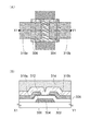
<CE構造(チャネルエッチ型)>
図1(A)は、本発明の一態様に係る半導体装置を示す平面図であり、図1(B)は、図1(A)に示すX1−Y1線に沿った断面図である。この半導体装置はボトムゲート構造(逆スタガ型構造ともいう)のトランジスタを有している。なお、図1(A)では、煩雑になることを避けるため、トランジスタの構成要素の一部(例えば、ゲート絶縁膜306など)を省略して図示している。
<CE structure (channel etch type)>
FIG. 1A is a plan view illustrating a semiconductor device according to one embodiment of the present invention, and FIG. 1B is a cross-sectional view taken along line X1-Y1 in FIG. This semiconductor device includes a transistor having a bottom gate structure (also referred to as an inverted staggered structure). Note that in FIG. 1A, some components (eg, the gate insulating film 306) are not illustrated in order to avoid complexity.
図1(B)に示すように、基板302上には下地絶縁膜(図示せず)が形成されている。この下地絶縁膜の表面から3nm以下の領域において、基板302中に含まれる金属元素の濃度が、1×10¹⁸atoms/cm3以下であることが好ましい。
As shown in FIG. 1B, a base insulating film (not shown) is formed over the
下地絶縁膜上にはゲート電極304が形成されている。下地絶縁膜及びゲート電極304の上にはゲート絶縁膜306が形成されており、ゲート絶縁膜306上にはチャネル領域を有する島状の酸化物半導体膜308が形成されている。酸化物半導体膜308は、ゲート絶縁膜306と接し、ゲート電極304と重畳する位置に設けられている。酸化物半導体膜308上及びゲート絶縁膜306上にはソース電極310a及びドレイン電極310bが形成されており、ソース電極310a及びドレイン電極310bは酸化物半導体膜308と電気的に接続されている。
A
酸化物半導体膜308には1〜50μm(好ましくは5μm未満)のチャネル長Lが形成されており、酸化物半導体膜308にはチャネル幅Wが形成されている(図1(A)参照)。また、酸化物半導体膜308をX線回折によって測定した回転角2θは31°近傍にピークを有し、酸化物半導体膜のバンドギャップは3.1eV以上であることが好ましい。なお、酸化物半導体膜308の詳細については後述する。
A channel length L of 1 to 50 μm (preferably less than 5 μm) is formed in the
トランジスタ上には、さらに層間絶縁膜312、及び平坦化絶縁膜314が設けられる構成としてもよい。詳細には、酸化物半導体膜308、ソース電極310a及びドレイン電極310bの上には層間絶縁膜312が設けられており、層間絶縁膜312上には平坦化絶縁膜314が設けられている。
An interlayer insulating
本実施の形態によれば、X線回折によって測定した回転角2θが31°近傍にピークを有し、バンドギャップが3.1eV以上である酸化物半導体膜308を用いることにより、チャネル長が短い酸化物半導体膜を用いたトランジスタであっても導通モード不良を抑制することができる。なお、本明細書等において、回転角2θが31°近傍にピークを有するとは、31°±1°の範囲を表す。
According to this embodiment, the channel length is short by using the
[酸化物半導体膜の詳細な説明]
酸化物半導体膜308は、CAAC−OS(C Axis Aligned Crystalline Oxide Semiconductor)膜であることが好ましい。
[Detailed description of oxide semiconductor film]
The
CAAC−OS膜は、完全な単結晶ではなく、完全な非晶質でもない。CAAC−OS膜は、非晶質相に結晶部を有する結晶−非晶質混相構造の酸化物半導体膜である。なお、当該結晶部は、一辺が100nm未満の立方体内に収まる大きさであることが多い。また、透過型電子顕微鏡(TEM:Transmission Electron Microscope)による観察像では、CAAC−OS膜に含まれる非晶質部と結晶部との境界は明確ではない。また、TEMによってCAAC−OS膜には粒界(グレインバウンダリーともいう)は確認できない。そのため、CAAC−OS膜は、粒界に起因する電子移動の低下が抑制される。 The CAAC-OS film is not completely single crystal nor completely amorphous. The CAAC-OS film is an oxide semiconductor film with a crystal-amorphous mixed phase structure where crystal parts are included in an amorphous phase. Note that the crystal part is often large enough to fit in a cube whose one side is less than 100 nm. Further, in the observation image obtained by a transmission electron microscope (TEM), the boundary between the amorphous part and the crystal part included in the CAAC-OS film is not clear. Further, a grain boundary (also referred to as a grain boundary) cannot be confirmed in the CAAC-OS film by TEM. Therefore, in the CAAC-OS film, reduction in electron transfer due to grain boundaries is suppressed.
CAAC−OS膜に含まれる結晶部は、c軸がCAAC−OS膜の被形成面の法線ベクトルまたは表面の法線ベクトルに平行な方向に揃い、かつab面に垂直な方向から見て三角形状または六角形状の原子配列を有し、c軸に垂直な方向から見て金属原子が層状または金属原子と酸素原子とが層状に配列している。なお、異なる結晶部間で、それぞれa軸およびb軸の向きが異なっていてもよい。本明細書等において、単に垂直と記載する場合、85°以上95°以下の範囲も含まれることとする。また、単に平行と記載する場合、−5°以上5°以下の範囲も含まれることとする。 In the crystal part included in the CAAC-OS film, the c-axis is aligned in a direction parallel to the normal vector of the formation surface of the CAAC-OS film or the normal vector of the surface, and triangular when viewed from the direction perpendicular to the ab plane. It has a shape or hexagonal atomic arrangement, and metal atoms are arranged in layers or metal atoms and oxygen atoms are arranged in layers as viewed from the direction perpendicular to the c-axis. Note that the directions of the a-axis and the b-axis may be different between different crystal parts. In this specification and the like, a simple term “vertical” includes a range from 85 ° to 95 °. In addition, a simple term “parallel” includes a range from −5 ° to 5 °.
なお、CAAC−OS膜において、結晶部の分布が一様でなくてもよい。例えば、CAAC−OS膜の形成過程において、酸化物半導体膜の表面側から結晶成長させる場合、表面の近傍では結晶部の占める割合が高くなることがある。また、CAAC−OS膜へ不純物を添加することにより、当該不純物添加領域において結晶部が非晶質化することもある。 Note that the distribution of crystal parts in the CAAC-OS film is not necessarily uniform. For example, in the formation process of the CAAC-OS film, when crystal growth is performed from the surface side of the oxide semiconductor film, the ratio of crystal parts in the vicinity of the surface might be high. In addition, when an impurity is added to the CAAC-OS film, the crystal part in a region to which the impurity is added becomes amorphous in some cases.
CAAC−OS膜に含まれる結晶部のc軸は、CAAC−OS膜の被形成面の法線ベクトルまたは表面の法線ベクトルに平行な方向に揃うため、CAAC−OS膜の形状(被形成面の断面形状または表面の断面形状)によっては互いに異なる方向を向くことがある。 Since the c-axis of the crystal part included in the CAAC-OS film is aligned in a direction parallel to the normal vector of the formation surface of the CAAC-OS film or the normal vector of the surface, the shape of the CAAC-OS film (formation surface) Depending on the cross-sectional shape of the surface or the cross-sectional shape of the surface).
なお、結晶部のc軸の方向は、CAAC−OS膜が形成されたときの被形成面の法線ベクトルまたは表面の法線ベクトルに平行な方向となる。結晶部は、成膜することにより、または成膜後に加熱処理などの結晶化処理を行うことにより形成される。 Note that the c-axis direction of the crystal part is parallel to the normal vector of the surface where the CAAC-OS film is formed or the normal vector of the surface. The crystal part is formed by film formation or by performing crystallization treatment such as heat treatment after film formation.
CAAC−OS膜を用いたトランジスタは、可視光や紫外光の照射によるトランジスタの電気特性の変動を低減することが可能である。また、しきい値の変動、及びバラツキを抑制できる。よって、当該トランジスタは信頼性が高い。 A transistor including a CAAC-OS film can reduce variation in electrical characteristics of the transistor due to irradiation with visible light or ultraviolet light. Further, fluctuations and variations in the threshold value can be suppressed. Therefore, the transistor has high reliability.
また、結晶部または結晶性を有する酸化物半導体膜では、よりバルク内欠陥を低減することができる。さらに、結晶部または結晶性を有する酸化物半導体膜表面の平坦性を高めることによって、該酸化物半導体膜を用いたトランジスタは、アモルファス状態の酸化物半導体膜を用いたトランジスタ以上の電界効果移動度を得ることができる。酸化物半導体膜表面の平坦性を高めるためには、平坦な表面上に酸化物半導体膜を形成することが好ましく、具体的には、平坦面粗さ(Ra)が0.15nm以下、好ましくは0.1nm以下の表面上に形成するとよい。 In an oxide semiconductor film having a crystal part or crystallinity, defects in the bulk can be further reduced. Further, by increasing planarity of a crystalline portion or a surface of an oxide semiconductor film having crystallinity, a transistor using the oxide semiconductor film has a higher field-effect mobility than a transistor using an amorphous oxide semiconductor film. Can be obtained. In order to improve the flatness of the surface of the oxide semiconductor film, it is preferable to form the oxide semiconductor film over a flat surface. Specifically, the flat surface roughness (Ra) is preferably 0.15 nm or less, preferably It is good to form on the surface of 0.1 nm or less.
なお、Raは、日本工業規格JIS B0601で定義されている中心線平均粗さを面に対して適用できるよう三次元に拡張したものであり、「基準面から指定面までの偏差の絶対値を平均した値」と表現でき、以下の式にて定義される。 Ra is a three-dimensional extension of the centerline average roughness defined in Japanese Industrial Standards JIS B0601 so that it can be applied to the surface. “The absolute value of the deviation from the reference surface to the specified surface is It can be expressed as “average value” and is defined by the following formula.

なお、上記において、S0は、測定面(座標(x1,y1)(x1,y2)(x2,y1)(x2,y2)で表される4点によって囲まれる長方形の領域)の面積を指し、Z0は測定面の平均高さを指す。Raは原子間力顕微鏡(AFM:Atomic Force Microscope)にて評価可能である。 In the above, S 0 is surrounded by four points represented by the measurement plane (coordinates (x 1 , y 1 ) (x 1 , y 2 ) (x 2 , y 1 ) (x 2 , y 2 )). (Rectangular region) indicates the area, and Z 0 indicates the average height of the measurement surface. Ra can be evaluated with an atomic force microscope (AFM).
また、酸化物半導体膜は、シリコンの1.1eVよりも大きい禁制帯幅を持つ酸化物半導体を適用することが好ましく、例えば、禁制帯幅が3.15eVであるIn−Ga−Zn系酸化物、禁制帯幅が約3.0eVである酸化インジウム、禁制帯幅が約3.0eVであるインジウム錫酸化物、禁制帯幅が約3.3eVであるインジウムガリウム酸化物、禁制帯幅が約2.7eVであるインジウム亜鉛酸化物、禁制帯幅が約3.3eVである酸化錫、禁制帯幅が約3.37eVである酸化亜鉛などを好ましく用いることができる。このような材料を用いることにより、トランジスタのオフ電流を極めて低く保つことが可能である。ただし、本発明の一態様では、酸化物半導体膜の禁制帯幅は3.1eV以上であることがより好ましい。 As the oxide semiconductor film, an oxide semiconductor having a forbidden band width larger than 1.1 eV of silicon is preferably used. For example, an In—Ga—Zn-based oxide having a forbidden band width of 3.15 eV is used. Indium oxide having a forbidden band width of about 3.0 eV, Indium tin oxide having a forbidden band width of about 3.0 eV, Indium gallium oxide having a forbidden band width of about 3.3 eV, Forbidden band width of about 2 Indium zinc oxide having a band gap of about 3.3 eV, tin oxide having a band gap of about 3.3 eV, zinc oxide having a band gap of about 3.37 eV, and the like can be preferably used. By using such a material, the off-state current of the transistor can be kept extremely low. However, in one embodiment of the present invention, the forbidden band width of the oxide semiconductor film is more preferably 3.1 eV or more.
また、酸化物半導体膜に用いる酸化物半導体としては、インジウム(In)、亜鉛(Zn)、及びガリウム(Ga)の群から選ばれた少なくとも一つを含むことが好ましい。特にInとZnを含むことが好ましい。また、該酸化物半導体を用いたトランジスタの電気特性のばらつきを減らすためのスタビライザーとしてスズ(Sn)を有することが好ましい。 The oxide semiconductor used for the oxide semiconductor film preferably contains at least one selected from the group of indium (In), zinc (Zn), and gallium (Ga). In particular, In and Zn are preferably included. In addition, it is preferable to include tin (Sn) as a stabilizer for reducing variation in electric characteristics of the transistor including the oxide semiconductor.
例えば、酸化物半導体として、酸化インジウム、酸化スズ、酸化亜鉛、二元系金属の酸化物であるIn−Zn系酸化物、Sn−Zn系酸化物、In−Ga系酸化物、三元系金属の酸化物であるIn−Ga−Zn系酸化物(IGZOとも表記する)、In−Sn−Zn系酸化物、Sn−Ga−Zn系酸化物、四元系金属の酸化物であるIn−Sn−Ga−Zn系酸化物を用いることができる。 For example, as an oxide semiconductor, indium oxide, tin oxide, zinc oxide, binary metal oxides In—Zn oxide, Sn—Zn oxide, In—Ga oxide, ternary metal In-Ga-Zn-based oxide (also referred to as IGZO), In-Sn-Zn-based oxide, Sn-Ga-Zn-based oxide, and In-Sn that is an oxide of a quaternary metal A -Ga-Zn-based oxide can be used.
ここで、In−Ga−Zn系酸化物とは、InとGaとZnを主成分として有する酸化物という意味であり、InとGaとZnの比率は問わない。また、InとGaとZn以外の金属元素が入っていてもよい。 Here, the In—Ga—Zn-based oxide means an oxide containing In, Ga, and Zn as main components, and there is no limitation on the ratio of In, Ga, and Zn. Moreover, metal elements other than In, Ga, and Zn may be contained.
また、酸化物半導体として、InMO3(ZnO)m(m>0、且つ、mは整数でない)で表記される材料を用いてもよい。なお、Mは、Ga、Fe、Mn及びCoから選ばれた一の金属元素もしくは複数の金属元素、または上記のスタビライザーとしての元素を示す。また、酸化物半導体として、In2SnO5(ZnO)n(n>0、且つ、nは整数)で表記される材料を用いてもよい。 Alternatively, a material represented by InMO 3 (ZnO) m (m> 0 is satisfied, and m is not an integer) may be used as the oxide semiconductor. Note that M represents one metal element or a plurality of metal elements selected from Ga, Fe, Mn, and Co, or the above-described element as a stabilizer. Alternatively, a material represented by In 2 SnO 5 (ZnO) n (n> 0 is satisfied, and n is an integer) may be used as the oxide semiconductor.
例えば、In:Ga:Zn=1:1:1、In:Ga:Zn=3:1:2、あるいはIn:Ga:Zn=2:1:3の原子数比のIn−Ga−Zn系酸化物やその組成の近傍の酸化物を用いるとよい。 For example, In: Ga: Zn = 1: 1: 1, In: Ga: Zn = 3: 1: 2, or In: Ga: Zn = 2: 1: 3 atomic ratio In—Ga—Zn-based oxidation An oxide in the vicinity of the product or its composition may be used.
また、酸化物半導体膜の成膜工程において、酸化物半導体膜に水素、または水がなるべく含まれないことが好ましい。例えば、酸化物半導体膜の成膜工程の前処理として、スパッタリング装置の予備加熱室で基板を予備加熱し、基板に吸着した水素、水分などの不純物を脱離し排気することが好ましい。また、酸化物半導体膜の成膜時、残留水分が排気された成膜室(成膜チャンバーともいう)で行うことが好ましい。 In the oxide semiconductor film formation step, it is preferable that hydrogen or water be contained as little as possible in the oxide semiconductor film. For example, it is preferable to preheat the substrate in a preheating chamber of a sputtering apparatus as a pretreatment for the oxide semiconductor film formation step, and to desorb and exhaust impurities such as hydrogen and moisture adsorbed on the substrate. The oxide semiconductor film is preferably formed in a deposition chamber (also referred to as a deposition chamber) from which residual moisture is exhausted.
なお、予備加熱室、及び成膜室の水分を除去するためには、吸着型の真空ポンプ、例えば、クライオポンプ、イオンポンプ、チタンサブリメーションポンプを用いることが好ましい。また、排気手段は、ターボポンプにコールドトラップを加えたものであってもよい。クライオポンプを用いて排気した、予備加熱室、及び成膜室は、例えば、水素原子、水(H2O)など水素原子を含む化合物(より好ましくは炭素原子を含む化合物も)等が排気されるため、酸化物半導体膜に含まれる水素、水分などの不純物の濃度を低減できる。 Note that in order to remove moisture from the preheating chamber and the deposition chamber, an adsorption-type vacuum pump such as a cryopump, an ion pump, or a titanium sublimation pump is preferably used. The exhaust means may be a turbo pump provided with a cold trap. In the preheating chamber and the film formation chamber exhausted using a cryopump, for example, a compound containing hydrogen atoms such as hydrogen atoms and water (H 2 O) (more preferably a compound containing carbon atoms) is exhausted. Therefore, the concentration of impurities such as hydrogen and moisture contained in the oxide semiconductor film can be reduced.
なお、酸化物半導体膜としてIn−Ga−Zn系酸化物をスパッタリング法により成膜する。また、酸化物半導体膜は、希ガス(代表的にはアルゴン)雰囲気下、酸素雰囲気下、または希ガスと酸素の混合雰囲気下においてスパッタリング法により形成することができる。 Note that an In—Ga—Zn-based oxide is formed as the oxide semiconductor film by a sputtering method. The oxide semiconductor film can be formed by a sputtering method in a rare gas (typically argon) atmosphere, an oxygen atmosphere, or a mixed atmosphere of a rare gas and oxygen.
酸化物半導体膜として、In−Ga−Zn系酸化物をスパッタリング法で作製するためのターゲットとしては、例えば、原子数比がIn:Ga:Zn=1:1:1の金属酸化物ターゲットや、原子数比がIn:Ga:Zn=3:1:2の金属酸化物ターゲットや、原子数比がIn:Ga:Zn=2:1:3の金属酸化物ターゲットを用いることができる。ただし、酸化物半導体膜に用いることのできるターゲットは、これらのターゲットの材料、及び組成に限定されるものではない。 As a target for manufacturing an In—Ga—Zn-based oxide by a sputtering method as an oxide semiconductor film, for example, a metal oxide target having an atomic ratio of In: Ga: Zn = 1: 1: 1, A metal oxide target having an atomic ratio of In: Ga: Zn = 3: 1: 2 or a metal oxide target having an atomic ratio of In: Ga: Zn = 2: 1: 3 can be used. Note that targets that can be used for the oxide semiconductor film are not limited to materials and compositions of these targets.
また、酸化物半導体膜を上述した金属酸化物ターゲットを用いて形成した場合、ターゲットの組成と、基板上に形成される薄膜の組成とが異なる場合がある。例えば、原子数比がIn:Ga:Zn=1:1:1の金属酸化物ターゲットを用いた場合、成膜条件にも依存するが、薄膜である酸化物半導体膜の組成比は、原子数比がIn:Ga:Zn=1:1:0.6〜0.8となる場合がある。これは、酸化物半導体膜の成膜中において、Znが昇華する、またはIn、Ga、Znの各成分のスパッタリングレートが異なるためであると考えられる。 In the case where the oxide semiconductor film is formed using the above-described metal oxide target, the composition of the target may be different from the composition of the thin film formed over the substrate. For example, in the case where a metal oxide target with an atomic ratio of In: Ga: Zn = 1: 1: 1 is used, the composition ratio of the oxide semiconductor film that is a thin film depends on the number of atoms, depending on the deposition conditions. The ratio may be In: Ga: Zn = 1: 1: 0.6 to 0.8. This is considered to be because Zn is sublimated during the formation of the oxide semiconductor film or the sputtering rate of each component of In, Ga, and Zn is different.
したがって、所望の組成比の薄膜を形成したい場合においては、予め金属酸化物ターゲットの組成比を調整する必要がある。例えば、薄膜である酸化物半導体膜の組成比を、原子数比がIn:Ga:Zn=1:1:1とする場合においては、金属酸化物ターゲットの組成比を、原子数比がIn:Ga:Zn=1:1:1.5とすればよい。すなわち、金属酸化物ターゲットのZnの含有量を予め多くすればよい。ただし、ターゲットの組成比は、上記数値に限定されず、成膜条件や、形成される薄膜の組成により適宜調整することができる。また、金属酸化物ターゲットのZnの含有量を多くすることにより、得られる薄膜の結晶性が向上するため好ましい。 Therefore, when it is desired to form a thin film having a desired composition ratio, it is necessary to adjust the composition ratio of the metal oxide target in advance. For example, in the case where the composition ratio of the thin oxide semiconductor film is an atomic ratio of In: Ga: Zn = 1: 1: 1, the composition ratio of the metal oxide target is the atomic ratio of In: Ga: Zn = 1: 1: 1.5 may be used. That is, the Zn content in the metal oxide target may be increased in advance. However, the composition ratio of the target is not limited to the above numerical values, and can be appropriately adjusted depending on the film forming conditions and the composition of the thin film to be formed. Further, increasing the Zn content of the metal oxide target is preferable because the crystallinity of the obtained thin film is improved.
また、金属酸化物ターゲットの相対密度は90%以上100%以下、好ましくは95%以上99.9%以下である。相対密度の高い金属酸化物ターゲットを用いることにより、成膜した酸化物半導体膜は緻密な膜とすることができる。 The relative density of the metal oxide target is 90% to 100%, preferably 95% to 99.9%. By using a metal oxide target having a high relative density, the formed oxide semiconductor film can be a dense film.
また、酸化物半導体膜を成膜する際に用いるスパッタリングガスとしては、水素、水、水酸基、または水素化物などの不純物が除去された高純度ガスを用いることが好ましい。 As a sputtering gas used for forming the oxide semiconductor film, a high-purity gas from which impurities such as hydrogen, water, a hydroxyl group, or hydride are removed is preferably used.
酸化物半導体膜として、CAAC−OS膜を適用する場合、該CAAC−OS膜を形成する方法としては、三つ挙げられる。一つめは、成膜温度を100℃以上450℃以下として酸化物半導体膜の成膜を行うことで、酸化物半導体膜に含まれる結晶部のc軸が、被形成面の法線ベクトルまたは表面の法線ベクトルに平行な方向に揃った結晶部を形成する方法である。二つめは、酸化物半導体膜を薄い膜厚で成膜した後、200℃以上700℃以下の熱処理を行うことで、酸化物半導体膜に含まれる結晶部のc軸が、被形成面の法線ベクトルまたは表面の法線ベクトルに平行な方向に揃った結晶部を形成する方法である。三つめは、一層目の酸化物半導体膜を薄く成膜した後、200℃以上700℃以下の熱処理を行い、さらに二層目の酸化物半導体膜の成膜を行うことで、酸化物半導体膜に含まれる結晶部のc軸が、被形成面の法線ベクトルまたは表面の法線ベクトルに平行な方向に揃った結晶部を形成する方法である。 In the case where a CAAC-OS film is used as the oxide semiconductor film, there are three methods for forming the CAAC-OS film. First, the oxide semiconductor film is formed at a deposition temperature of 100 ° C. to 450 ° C. so that the c-axis of the crystal part included in the oxide semiconductor film is a normal vector of the surface to be formed or the surface This is a method for forming crystal parts aligned in a direction parallel to the normal vector. Second, after the oxide semiconductor film is formed with a small thickness, heat treatment is performed at 200 ° C. to 700 ° C. so that the c-axis of the crystal part included in the oxide semiconductor film is a method of forming a surface. This is a method of forming a crystal part aligned in a direction parallel to a line vector or a surface normal vector. Third, after forming a thin oxide semiconductor film of the first layer, heat treatment at 200 ° C. to 700 ° C. is performed, and further, a second oxide semiconductor film is formed. In which the c-axis of the crystal part is aligned in a direction parallel to the normal vector of the surface to be formed or the normal vector of the surface.
また、基板を加熱しながら成膜することにより、成膜した酸化物半導体膜に含まれる水素や水などの不純物濃度を低減することができる。また、スパッタリングによる損傷が軽減されるため好ましい。また、酸化物半導体膜を、ALD(Atomic Layer Deposition)法、蒸着法、塗布法などで成膜してもよい。 In addition, by forming a film while heating the substrate, the concentration of impurities such as hydrogen and water contained in the formed oxide semiconductor film can be reduced. Further, it is preferable because damage due to sputtering is reduced. Alternatively, the oxide semiconductor film may be formed by an ALD (Atomic Layer Deposition) method, an evaporation method, a coating method, or the like.
なお、酸化物半導体膜として、CAAC−OS膜以外の結晶性を有する酸化物半導体膜(単結晶または微結晶)を成膜する場合には、成膜温度は特に限定されない。 Note that in the case where an oxide semiconductor film (single crystal or microcrystal) having crystallinity other than the CAAC-OS film is formed as the oxide semiconductor film, the deposition temperature is not particularly limited.
また、酸化物半導体膜の加工方法としては、ウエットエッチング法、またはドライエッチング法により酸化物半導体膜のエッチングを行うことができる。ドライエッチング法のエッチングガスには、BCl3、Cl2、O2等を用いることができる。エッチング速度の向上にはECR(Electron Cycrotron Resonance)やICP(Inductive Coupled Plasma)などの高密度プラズマ源を用いたドライエッチング装置を用いることができる。 As a method for processing the oxide semiconductor film, the oxide semiconductor film can be etched by a wet etching method or a dry etching method. BCl 3 , Cl 2 , O 2, or the like can be used as an etching gas for the dry etching method. A dry etching apparatus using a high-density plasma source such as ECR (Electron Cyclotron Resonance) or ICP (Inductive Coupled Plasma) can be used to improve the etching rate.
また、酸化物半導体膜の形成後、酸化物半導体膜に対して、熱処理を行ってもよい。当該熱処理の温度は、300℃以上700℃以下、または基板の歪み点未満とする。当該熱処理を行うことで、酸化物半導体膜に含まれる過剰な水素(水や水酸基を含む)を除去することが可能である。なお、当該熱処理は、本明細書等において、脱水化処理(脱水素化処理)と記す場合がある。 Further, after the oxide semiconductor film is formed, heat treatment may be performed on the oxide semiconductor film. The temperature of the heat treatment is 300 ° C. or higher and 700 ° C. or lower, or lower than the strain point of the substrate. By performing the heat treatment, excess hydrogen (including water and a hydroxyl group) contained in the oxide semiconductor film can be removed. Note that the heat treatment may be referred to as dehydration treatment (dehydrogenation treatment) in this specification and the like.
当該熱処理は、例えば、抵抗発熱体などを用いた電気炉に被処理物を導入し、窒素雰囲気下、450℃、1時間の条件で行うことができる。この間、酸化物半導体膜は大気に触れさせず、水や水素の混入が生じないようにする。 The heat treatment can be performed, for example, by introducing an object to be processed into an electric furnace using a resistance heating element and the like under a nitrogen atmosphere at 450 ° C. for one hour. During this time, the oxide semiconductor film is not exposed to the air so that water and hydrogen are not mixed.
熱処理装置は、電気炉に限られず、加熱されたガスなどの媒体からの熱伝導、または熱輻射によって、被処理物を加熱する装置を用いてもよい。例えば、GRTA(Gas Rapid Thermal Anneal)装置、LRTA(Lamp Rapid Thermal Anneal)装置等のRTA(Rapid Thermal Anneal)装置を用いることができる。LRTA装置は、ハロゲンランプ、メタルハライドランプ、キセノンアークランプ、カーボンアークランプ、高圧ナトリウムランプ、高圧水銀ランプなどのランプから発する光(電磁波)の輻射により、被処理物を加熱する装置である。GRTA装置は、高温のガスを用いて熱処理を行う装置である。ガスとしては、アルゴンなどの希ガス、または窒素のような、熱処理によって被処理物と反応しない不活性気体が用いられる。 The heat treatment apparatus is not limited to an electric furnace, and an apparatus for heating an object to be processed by heat conduction or heat radiation from a medium such as a heated gas may be used. For example, a rapid thermal annealing (RTA) device such as a GRTA (Gas Rapid Thermal Anneal) device or an LRTA (Lamp Rapid Thermal Anneal) device can be used. The LRTA apparatus is an apparatus that heats an object to be processed by radiation of light (electromagnetic waves) emitted from a lamp such as a halogen lamp, a metal halide lamp, a xenon arc lamp, a carbon arc lamp, a high pressure sodium lamp, or a high pressure mercury lamp. The GRTA apparatus is an apparatus that performs heat treatment using a high-temperature gas. As the gas, an inert gas that does not react with an object to be processed by heat treatment, such as nitrogen or a rare gas such as argon, is used.
例えば、当該熱処理として、熱せられた不活性ガス雰囲気中に被処理物を投入し、数分間熱した後、当該不活性ガス雰囲気から被処理物を取り出すGRTA処理を行ってもよい。GRTA処理を用いると短時間での高温熱処理が可能となる。また、被処理物の耐熱温度を超える温度条件であっても適用が可能となる。なお、処理中に、不活性ガスを、酸素を含むガスに切り替えても良い。 For example, as the heat treatment, a GRTA process may be performed in which an object to be processed is put in a heated inert gas atmosphere, heated for several minutes, and then the object to be processed is taken out from the inert gas atmosphere. When GRTA treatment is used, high-temperature heat treatment can be performed in a short time. In addition, application is possible even under temperature conditions exceeding the heat resistance temperature of the object to be processed. Note that the inert gas may be switched to a gas containing oxygen during the treatment.
なお、不活性ガス雰囲気としては、窒素、または希ガス(ヘリウム、ネオン、アルゴン等)を主成分とする雰囲気であって、水、水素などが含まれない雰囲気を適用するのが望ましい。例えば、熱処理装置に導入する窒素や、ヘリウム、ネオン、アルゴン等の希ガスの純度を、6N(99.9999%)以上、好ましくは7N(99.99999%)以上(すなわち、不純物濃度が1ppm以下、好ましくは0.1ppm以下)とする。 Note that as the inert gas atmosphere, an atmosphere containing nitrogen or a rare gas (such as helium, neon, or argon) as a main component and not including water, hydrogen, or the like is preferably used. For example, the purity of nitrogen or a rare gas such as helium, neon, or argon introduced into the heat treatment apparatus is 6N (99.9999%) or more, preferably 7N (99.99999%) or more (that is, the impurity concentration is 1 ppm or less). , Preferably 0.1 ppm or less).
また、上述の脱水化処理(脱水素化処理)を行うと、酸化物半導体膜を構成する主成分材料である酸素が同時に脱離して減少してしまうおそれがある。酸化物半導体膜において、酸素が脱離した箇所では酸素欠損が存在し、該酸素欠損に起因してトランジスタの電気的特性変動を招くドナー準位が生じてしまう。よって、脱水化処理(脱水素化処理)を行った場合、酸化物半導体膜中に、酸素を供給することが好ましい。酸化物半導体膜中に酸素を供給することにより、膜中の酸素欠損を補填することができる。 Further, when the above-described dehydration treatment (dehydrogenation treatment) is performed, oxygen that is a main component material included in the oxide semiconductor film may be simultaneously desorbed and reduced. In the oxide semiconductor film, oxygen vacancies exist at locations where oxygen is released, and donor levels that cause fluctuations in electrical characteristics of the transistor are generated due to the oxygen vacancies. Therefore, when dehydration treatment (dehydrogenation treatment) is performed, oxygen is preferably supplied to the oxide semiconductor film. By supplying oxygen into the oxide semiconductor film, oxygen vacancies in the film can be filled.
酸化物半導体膜中の酸素欠損を補填する方法の一例としては、酸化物半導体膜に対して脱水化処理(脱水素化処理)を行った後、同じ炉に高純度の酸素ガス、二窒化酸素ガス、高純度の亜酸化窒素ガス、又は超乾燥エア(CRDS(キャビティリングダウンレーザー分光法)方式の露点計を用いて測定した場合の水分量が20ppm(露点換算で−55℃)以下、好ましくは1ppm以下、より好ましくは10ppm以下の空気)を導入すればよい。酸素ガス、または二窒化酸素ガスに、水、水素などが含まれないことが好ましい。または、熱処理装置に導入する酸素ガス、または二窒化酸素ガスの純度を、6N(99.9999%)以上、好ましくは7N(99.99999%)以上(即ち、酸素ガスまたは二窒化酸素ガス中の不純物濃度を1ppm以下、好ましくは0.1ppm以下)とすることが好ましい。 As an example of a method for filling oxygen vacancies in an oxide semiconductor film, after dehydration treatment (dehydrogenation treatment) is performed on the oxide semiconductor film, high-purity oxygen gas or oxygen dinitride is supplied to the same furnace. Gas, high-purity nitrous oxide gas, or ultra-dry air (CRDS (cavity ring-down laser spectroscopy) method) using a dew point meter of 20 ppm (-55 ° C in terms of dew point) or less, preferably 1 ppm or less, more preferably 10 ppm or less. It is preferable that water, hydrogen, or the like be not contained in the oxygen gas or the oxygen dinitride gas. Alternatively, the purity of the oxygen gas or oxygen dinitride gas introduced into the heat treatment apparatus is 6N (99.9999%) or higher, preferably 7N (99.99999%) or higher (that is, in oxygen gas or oxygen dinitride gas). The impurity concentration is preferably 1 ppm or less, preferably 0.1 ppm or less.
また、酸化物半導体膜中に酸素を供給する方法の一例としては、酸化物半導体膜に酸素(少なくとも、酸素ラジカル、酸素原子、酸素イオンのいずれかを含む)を添加することで、酸化物半導体膜中に酸素を供給してもよい。酸素の添加方法としては、イオン注入法、イオンドーピング法、プラズマイマージョンイオンインプランテーション法、プラズマ処理などを用いることができる。 As an example of a method for supplying oxygen into the oxide semiconductor film, an oxide semiconductor can be obtained by adding oxygen (including at least one of oxygen radicals, oxygen atoms, and oxygen ions) to the oxide semiconductor film. Oxygen may be supplied into the film. As an oxygen addition method, an ion implantation method, an ion doping method, a plasma immersion ion implantation method, a plasma treatment, or the like can be used.
また、酸化物半導体膜中に酸素を供給する方法の一例としては、下地絶縁膜、または後に形成されるゲート絶縁膜等を加熱することにより、酸素の一部を脱離させ、酸化物半導体膜に酸素を供給してもよい。 As an example of a method for supplying oxygen into the oxide semiconductor film, part of oxygen is released by heating the base insulating film or a gate insulating film to be formed later, so that the oxide semiconductor film Oxygen may be supplied.
上述のように、酸化物半導体膜の形成後において、脱水化処理(脱水素化処理)を行い酸化物半導体膜から、水素、または水分を除去して不純物が極力含まれないように高純度化し、脱水化処理(脱水素化処理)によって同時に減少してしまった酸素を酸化物半導体に加える、または過剰な酸素を供給し酸化物半導体膜の酸素欠損を補填することが好ましい。また、酸化物半導体膜に酸素を供給する場合を、加酸素化処理、または過酸素化処理と記す場合がある。 As described above, after the oxide semiconductor film is formed, dehydration treatment (dehydrogenation treatment) is performed to remove hydrogen or moisture from the oxide semiconductor film so that impurities are contained as little as possible. It is preferable to add oxygen that has been simultaneously reduced by dehydration treatment (dehydrogenation treatment) to the oxide semiconductor, or supply excess oxygen to fill oxygen vacancies in the oxide semiconductor film. The case where oxygen is supplied to the oxide semiconductor film may be referred to as oxygenation treatment or peroxygenation treatment.
このように、酸化物半導体膜は、脱水化処理(脱水素化処理)により、水素または水分が除去され、加酸素化処理により酸素欠損を補填することによって、電気的にi型(真性)化またはi型に限りなく近い酸化物半導体膜とすることができる。具体的には、酸化物半導体膜中の水素濃度は、5×10¹⁹atoms/cm3以下、好ましくは5×1018atoms/cm3以下、さらに好ましくは5×1017atoms/cm3以下とする。なお、上述の酸化物半導体膜中の水素濃度は、二次イオン質量分析法(SIMS:Secondary Ion Mass Spectroscopy)で測定されるものである。 In this manner, the oxide semiconductor film is electrically i-type (intrinsic) by removing hydrogen or moisture by dehydration treatment (dehydrogenation treatment) and filling oxygen vacancies by oxygenation treatment. Alternatively, an oxide semiconductor film which is almost as i-type can be obtained. Specifically, the hydrogen concentration in the oxide semiconductor film is 5 × 10 19 atoms / cm 3 or less, preferably 5 × 10 18 atoms / cm 3 or less, more preferably 5 × 10 17 atoms / cm 3 or less. To do. Note that the hydrogen concentration in the oxide semiconductor film is measured by secondary ion mass spectrometry (SIMS).
このように、水素濃度が十分に低減されて高純度化され、十分な酸素の供給により酸素欠乏に起因するエネルギーギャップ中の欠陥準位が低減された酸化物半導体膜では、ドナーに由来するキャリアが極めて少なく(ゼロに近い)、キャリア濃度が1×10¹²/cm3
未満、好ましくは1×10¹¹/cm3未満、さらに好ましくは、1.45×1010/cm3未満となる。このような酸化物半導体膜を用いたトランジスタにおいて、例えば、室温(25℃)でのオフ電流(ここでは、単位チャネル幅(1μm)あたりの値)は、100zA(1zA(ゼプトアンペア)は1×10−21A)以下、好ましくは10zA以下、さらに好ましくは100yA(1yA(ヨクトアンペア)は1×10−24A)以下となる。このように、i型化(真性化)または実質的にi型化された酸化物半導体を用いることで、極めて優れたオフ電流特性のトランジスタとすることができる。
In this manner, in the oxide semiconductor film in which the hydrogen concentration is sufficiently reduced to be highly purified and the defect level in the energy gap due to oxygen deficiency is reduced by supplying sufficient oxygen, the carrier derived from the donor Is very small (close to zero) and the carrier concentration is 1 × 10 12 / cm 3.
Less, preferably less than 1 × 10 11 / cm 3 , more preferably less than 1.45 × 10 10 / cm 3 . In a transistor including such an oxide semiconductor film, for example, an off current at room temperature (25 ° C.) (here, a value per unit channel width (1 μm)) is 100 zA (1 zA (zeptoampere) is 1 × 10 −21 A) or less, preferably 10 zA or less, and more preferably 100 yA (1 yA (yokutoampere) is 1 × 10 −24 A) or less. In this manner, by using an i-type (intrinsic) or substantially i-type oxide semiconductor, a transistor with extremely excellent off-state current characteristics can be obtained.
<トランジスタの作製方法>
図1(B)に示した半導体装置の作製方法について説明する。
まず、基板302上に下地絶縁膜(図示せず)を形成する。
<Method for Manufacturing Transistor>
A method for manufacturing the semiconductor device illustrated in FIG. 1B will be described.
First, a base insulating film (not shown) is formed over the
基板302としては、アルミノシリケートガラス、アルミノホウケイ酸ガラス、バリウムホウケイ酸ガラスなどのガラス材料を用いる。量産する上では、基板102は、第8世代(2160mm×2460mm)、第9世代(2400mm×2800mm、または2450mm×3050mm)、第10世代(2950mm×3400mm)等のマザーガラスを用いることが好ましい。マザーガラスは、処理温度が高く、処理時間が長いと大幅に収縮するため、マザーガラスを使用して量産を行う場合、作製工程の加熱処理は、好ましくは600℃以下、さらに好ましくは450℃以下、さらに好ましくは350℃以下とすることが望ましい。
As the
下地絶縁膜としては、例えば、酸化シリコン、酸化窒化シリコン、窒化酸化シリコン、窒化シリコン、または酸化アルミニウム膜等を用いることができる。酸化アルミニウム膜は、スパッタリング法により形成し、好ましくは密度が3.2g/cm3以上、さらに好ましくは3.6g/cm3以上であるとよい。下地絶縁膜として、上述した酸化アルミニウム膜を用いることで、基板302からトランジスタ中に拡散する不純物を防止することができる。基板302からの不純物としては、例えば、水素、金属元素等がある。金属元素としては、ナトリウム、アルミニウム、マグネシウム、カルシウム、ストロンチウム、バリウム、シリコン、ボロンといった元素が挙げられる。また、下地絶縁膜の膜厚は、5nm以上150nm以下(好ましくは10nm以上100nm以下)とすることができる。
As the base insulating film, for example, silicon oxide, silicon oxynitride, silicon nitride oxide, silicon nitride, an aluminum oxide film, or the like can be used. The aluminum oxide film is formed by a sputtering method, and preferably has a density of 3.2 g / cm 3 or more, more preferably 3.6 g / cm 3 or more. By using the above-described aluminum oxide film as the base insulating film, impurities that diffuse from the
下地絶縁膜の表面から3nm以下の領域において、ガラス基板中に含まれる金属元素の濃度が、1×10¹⁸atoms/cm3以下であることが好ましい。 In the region of 3 nm or less from the surface of the base insulating film, the concentration of the metal element contained in the glass substrate is preferably 1 × 10 18 atoms / cm 3 or less.
また、下地絶縁膜としては、水(H2O)、または水素(H2)の放出量が少ない膜が好ましい。例えば、下地絶縁膜として、酸化アルミニウム膜を用いることができる。酸化アルミニウム膜の水(H2O)の放出量が、好ましくは5×10¹⁵atoms/cm3以下、さらに好ましくは1×1015atoms/cm3以下であるとよい。また、酸化アルミニウム膜の水素(H2)の放出量が、好ましくは5×1015atoms/cm3以下、さらに好ましくは1×1015atoms/cm3以下であるとよい。 In addition, as the base insulating film, a film that releases less water (H 2 O) or hydrogen (H 2 ) is preferable. For example, an aluminum oxide film can be used as the base insulating film. The amount of water (H 2 O) released from the aluminum oxide film is preferably 5 × 10 15 atoms / cm 3 or less, more preferably 1 × 10 15 atoms / cm 3 or less. The amount of hydrogen (H 2 ) released from the aluminum oxide film is preferably 5 × 10 15 atoms / cm 3 or less, more preferably 1 × 10 15 atoms / cm 3 or less.
例えば、下地絶縁膜の膜中に水素、または水の放出量が多い膜を用いると、トランジスタの形成工程中に下地絶縁膜から水、または水素が放出し、トランジスタ中の酸化物半導体膜308内に拡散する可能性がある。そのため、上述した放出量の下地絶縁膜とすることで、トランジスタに拡散する不純物を抑制し、信頼性の高い半導体装置とすることができる。
For example, when a film with a large amount of hydrogen or water released is used for the base insulating film, water or hydrogen is released from the base insulating film during the transistor formation process, and the
なお、上述した水の放出量、及び水素の放出量は、昇温脱離ガス分光法(TDS:Thermal Desorption Spectroscopy)により、測定することができる。 Note that the above-described water release amount and hydrogen release amount can be measured by temperature-desorption gas spectroscopy (TDS: Thermal Desorption Spectroscopy).
次に、下地絶縁膜上に、導電膜を形成した後、フォトリソグラフィ工程、及びエッチング工程によりゲート電極304を形成し、その後、下地絶縁膜、及びゲート電極304上にゲート絶縁膜306を形成する。
Next, after a conductive film is formed over the base insulating film, the
ゲート電極304としては、スパッタリング法等により、モリブデン、チタン、タンタル、タングステン、アルミニウム、銅、ネオジム、及びスカンジウム等の金属材料、または、これらの少なくとも一つを含む合金材料を用いて、単層、または積層して形成することができる。
As the
ゲート絶縁膜306としては、例えば、PE−CVD法等により、酸化シリコン、酸化ガリウム、酸化アルミニウム、窒化シリコン、酸化窒化シリコン、酸化窒化アルミニウム、または窒化酸化シリコン等を用いることができる。また、ゲート絶縁膜306の膜厚としては、例えば、10nm以上500nm以下、好ましくは50nm以上300nm以下とすることができる。また、ゲート絶縁膜306として、基板302からの不純物の拡散を防止できる膜とすることで、下地絶縁膜を設けない構成とすることもできる。
As the
また、ゲート絶縁膜306は、のちに形成される酸化物半導体膜308と接する部分において酸素を含むことが好ましい。特に、ゲート絶縁膜306は、膜中に少なくとも化学量論的組成比を超える量の酸素が存在することが好ましく、例えば、ゲート絶縁膜306として、酸化シリコンを用いる場合には、SiO2+α(ただし、α>0)とすることが好ましい。本実施の形態では、ゲート絶縁膜306として、SiO2+α(ただし、α>0)である酸化シリコンを用いる。この酸化シリコンをゲート絶縁膜306として用いることで、のちに形成される酸化物半導体膜308に酸素を供給することができ、酸化物半導体膜308の電気特性を良好にすることができる。
The
また、ゲート絶縁膜306のその他の材料としては、酸化ハフニウム、酸化イットリウム、ハフニウムシリケート(HfSixOy(x>0、y>0))、窒素が添加されたハフニウムシリケート(HfSiOxNy(x>0、y>0))、ハフニウムアルミネート(HfAlxOy(x>0、y>0))、酸化ランタンなどのhigh−k材料を用いることができる。このような材料を用いることでゲートリーク電流を低減できる。さらに、ゲート絶縁膜306は、単層構造としても良いし、積層構造としても良い。
Other materials for the
次に、ゲート絶縁膜306が形成された基板302に対して、加熱処理を行っても良い。
Next, heat treatment may be performed on the
例えば、加熱処理としては、電気炉、もしくは抵抗発熱体などの発熱体からの熱伝導または熱輻射によって、被処理物を加熱する装置を用いることができ、GRTA(Gas Rapid Thermal Anneal)装置、LRTA(Lamp Rapid Thermal Anneal)装置等のRTA(Rapid Thermal Anneal)装置を用いることができる。LRTA装置は、ハロゲンランプ、メタルハライドランプ、キセノンアークランプ、カーボンアークランプ、高圧ナトリウムランプ、高圧水銀ランプなどのランプから発する光(電磁波)の輻射により、被処理物を加熱する装置である。GRTA装置は、高温のガスを用いて加熱処理を行う装置である。高温のガスには、アルゴンなどの希ガス、または窒素のような、加熱処理によって被処理物と反応しない不活性気体が用いられる。また、高温のガスのその他の一例としては、酸素を用いてもよい。酸素を用いることにより、ゲート絶縁膜306からの酸素の脱離を抑制、またはゲート絶縁膜306へ酸素の供給を行うことができる。
For example, as the heat treatment, an apparatus for heating an object to be processed by heat conduction or heat radiation from an electric furnace or a heating element such as a resistance heating element can be used. A GRTA (Gas Rapid Thermal Anneal) apparatus, LRTA An RTA (Rapid Thermal Anneal) apparatus such as a (Lamp Rapid Thermal Anneal) apparatus can be used. The LRTA apparatus is an apparatus that heats an object to be processed by radiation of light (electromagnetic waves) emitted from a lamp such as a halogen lamp, a metal halide lamp, a xenon arc lamp, a carbon arc lamp, a high pressure sodium lamp, or a high pressure mercury lamp. The GRTA apparatus is an apparatus that performs heat treatment using a high-temperature gas. As the high-temperature gas, an inert gas that does not react with an object to be processed by heat treatment, such as nitrogen or a rare gas such as argon, is used. As another example of the high temperature gas, oxygen may be used. By using oxygen, desorption of oxygen from the
加熱処理の処理温度としては、基板302として、マザーガラスを用いた場合、処理温度が高く、処理時間が長いと大幅に収縮するため、好ましくは、200℃以上450℃以下、さらに好ましくは、250℃以上350℃以下である。
As the processing temperature of the heat treatment, when mother glass is used as the
なお、上記加熱処理を行うことで、ゲート絶縁膜306の膜中に含まれる水、水素等の不純物を除去することができる。また、当該加熱処理により、ゲート絶縁膜306の膜中の欠陥密度を低減することができる。ゲート絶縁膜306の膜中の不純物、または膜中の欠陥密度が低減することにより、半導体装置の信頼性が向上する。例えば、半導体装置の信頼性試験の一つである光負バイアスストレス試験における半導体装置の劣化を抑制させることができる。
Note that by performing the heat treatment, impurities such as water and hydrogen contained in the
また、上記加熱処理は、のちに形成される酸化物半導体膜308の成膜前処理として、行ってもよい。例えば、ゲート絶縁膜306を形成した後、スパッタリング装置の予備加熱室にて、真空中で加熱処理を行った後、酸化物半導体膜308を形成してもよい。
Further, the heat treatment may be performed as pretreatment for forming the
また、上記加熱処理は、複数回行ってもよい。例えば、ゲート絶縁膜306の形成後、電気炉等により窒素雰囲気中で加熱処理を行い、その後、スパッタリング装置の予備加熱室にて、真空中で加熱処理を行った後、酸化物半導体膜308を形成してもよい。
Further, the heat treatment may be performed a plurality of times. For example, after the
次に、ゲート絶縁膜306上に、酸化物半導体膜を成膜し、フォトリソグラフィ工程、及びエッチング工程を行い、島状の酸化物半導体膜308を形成する。
Next, an oxide semiconductor film is formed over the
酸化物半導体膜308の詳細な内容及び作製方法等については、[酸化物半導体膜の詳細な説明]の欄に記載したが、本発明の一態様では、基板302を加熱し、酸素ガス及び希ガスを用いた第1及び第2の条件で、In−Ga−Zn系酸化物ターゲットをスパッタリングすることにより、ゲート絶縁膜306上に酸化物半導体膜を形成し、この酸化物半導体膜を加工することにより、ゲート絶縁膜306上に活性層としての酸化物半導体膜306を形成することが好ましい。第1の条件は、基板302の加熱温度が100℃以上で且つ酸素ガスの流量比が70%以上であり、第2の条件は、基板302の加熱温度が170℃以上で且つ酸素ガスの流量比が30%以上であることが好ましい。このようにして、X線回折によって測定した回転角2θが31°近傍にピークを有し、且つバンドギャップが3.1eV以上である酸化物半導体膜308を作製することができる。
The detailed content and manufacturing method of the
次に、ゲート絶縁膜306及び酸化物半導体膜308の上に導電膜を形成し、当該導電膜にフォトリソグラフィ工程、及びエッチング工程を行い、酸化物半導体膜308に電気的に接続されたソース電極310a及びドレイン電極310bを形成する。酸化物半導体膜308のチャネル長Lは1〜50μmであり、好ましくは5μm未満である。なお、この段階でトランジスタが形成される。
Next, a conductive film is formed over the
ソース電極310a及びドレイン電極310bに用いる導電膜としては、例えば、Al、Cr、Cu、Ta、Ti、Mo、Wから選ばれた元素を含む金属膜、または上述した元素を成分とする金属窒化物膜(窒化チタン膜、窒化モリブデン膜、窒化タングステン膜)等を用いることができる。また、Al、Cuなどの金属膜の下側又は上側の一方または双方にTi、Mo、Wなどの高融点金属膜、またはそれらの金属窒化物膜(窒化チタン膜、窒化モリブデン膜、窒化タングステン膜)を積層させた構成としても良い。
As the conductive film used for the
次に、トランジスタ上に、層間絶縁膜312及び平坦化絶縁膜314を形成する。層間絶縁膜312としては、ゲート絶縁膜306に用いた材料及び方法と、同様な材料及び方法により形成することができる。
Next, an
平坦化絶縁膜314としては、例えば、ポリイミド、アクリル、ベンゾシクロブテン、等の有機樹脂材料を用いることができる。平坦化絶縁膜314により、トランジスタの凹凸を低減させることができる。
As the
また、平坦化絶縁膜314上に導電膜を形成してもよい(図示しない)。導電膜としては、例えば、酸化インジウム−酸化スズ(ITO:Indium Tin Oxide)、または酸化インジウム−酸化亜鉛などの透光性を有する導電材料を用いることができる。ただし、導電膜として用いることのできる材料は、上記材料に限定されない。例えば、金属膜(アルミニウム、チタンなど)を用いることもできる。このような金属膜を用いることにより、トランジスタを外光から遮光することができるので、好適である。 Further, a conductive film may be formed over the planarization insulating film 314 (not illustrated). As the conductive film, a light-transmitting conductive material such as indium oxide-tin oxide (ITO) or indium oxide-zinc oxide can be used, for example. Note that a material that can be used for the conductive film is not limited to the above materials. For example, a metal film (aluminum, titanium, etc.) can also be used. Use of such a metal film is preferable because the transistor can be shielded from external light.
なお、上述した導電膜は、外部からの静電気(所謂、ESD:Electro Static Discharge)に対して、トランジスタを保護する機能も有する。トランジスタ上に導電膜を有することで、外部からの静電気放電等の電荷を当該導電膜により、逃がすことができる。 Note that the above-described conductive film also has a function of protecting the transistor against external static electricity (so-called ESD: Electro Static Discharge). With the conductive film over the transistor, charges such as external electrostatic discharge can be released by the conductive film.
以上の工程により、図1(B)に示す半導体装置を作製することができる。 Through the above steps, the semiconductor device illustrated in FIG. 1B can be manufactured.
チャネルエッチ構造においては、バックチャネル側はチャネルエッチの際にプラズマ処理に曝される。チャネル長Lが長ければ活性層における欠損の発生確率の関係で導通モード不良が発生しにくいが、チャネル長Lが短いと導通モード不良が発生しやすくなる。しかし、本発明の一態様に係るチャネルエッチ構造では、X線回折によって測定した回転角2θが31°近傍にピークを有し、バンドギャップが3.1eV以上であるIGZOからなる酸化物半導体膜308を用いることにより、その酸化物半導体膜308における欠損の発生確率を低くすることができ、導通モード不良が抑制できる。
In the channel etch structure, the back channel side is exposed to plasma processing during channel etch. If the channel length L is long, the conduction mode failure is less likely to occur due to the probability of occurrence of defects in the active layer, but if the channel length L is short, the conduction mode failure tends to occur. However, in the channel etch structure according to one embodiment of the present invention, the
以上説明したように、チャネル長Lが短い酸化物半導体膜を用いたトランジスタであっても導通モード不良を抑制できるため、チャネル長の短いトランジスタが作製可能になり、チャネル長を5μm未満または2μm以下とすることが可能となる。その結果、広い範囲でのチャネル長/チャネル幅(L/W)サイズのトランジスタが作製可能になる。また、チャネル長を短くできるため、トランジスタのサイズを小さくできる。従って、パネルに用いる場合は、開口率向上や高精細化に有利となり、ドライバに用いる場合は、ドライバ領域を小さくでき、額縁を小さくできる。 As described above, since a conduction mode failure can be suppressed even with a transistor using an oxide semiconductor film with a short channel length L, a transistor with a short channel length can be manufactured, and the channel length is less than 5 μm or 2 μm or less. It becomes possible. As a result, a transistor having a channel length / channel width (L / W) size in a wide range can be manufactured. In addition, since the channel length can be shortened, the size of the transistor can be reduced. Therefore, when used for a panel, it is advantageous for improving the aperture ratio and increasing the definition, and when used for a driver, the driver area can be reduced and the frame can be reduced.
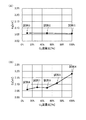
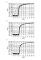
本実施例では、インジウム、ガリウム、及び亜鉛を含む酸化物半導体膜(以下、「IGZO膜」と表す)を作製し、作製したIGZO膜のバンドギャップ(エネルギーギャップとも言う、以下「Eg」と表す)、及び結晶性について、評価を行った。なお、Egについては、IGZO膜の分光エリプソメトリーで測定して得られた値を評価し、結晶性については、IGZO膜のX線回折(XRD:X−Ray Diffraction、以下、「XRD測定」と表す)測定による評価を行った。 In this example, an oxide semiconductor film containing indium, gallium, and zinc (hereinafter referred to as an “IGZO film”) was manufactured, and a band gap (also referred to as an energy gap, hereinafter referred to as “Eg”) of the manufactured IGZO film. ) And crystallinity were evaluated. In addition, about Eg, the value obtained by measuring by spectroscopic ellipsometry of the IGZO film was evaluated, and for crystallinity, X-ray diffraction of the IGZO film (XRD: X-Ray Diffraction, hereinafter referred to as “XRD measurement”) Representation) Evaluation by measurement was performed.
また、作製したIGZO膜は、In:Ga:Zn=1:1:1(原子数比)の金属酸化物ターゲットを用い、成膜圧力=0.6Pa、成膜電力=5kw、膜厚=100nmを固定の条件とし、基板温度、及びO2流量(O2流量比)の条件振りを行い、試料1乃至試料18を作製した。以下に試料1乃至試料18の条件の詳細を示す。
The manufactured IGZO film uses a metal oxide target of In: Ga: Zn = 1: 1: 1 (atomic ratio), a deposition pressure = 0.6 Pa, a deposition power = 5 kW, and a film thickness = 100 nm. Was set as a fixed condition, and the conditions of the substrate temperature and the O 2 flow rate (O 2 flow rate ratio) were varied to prepare
(試料1)
基板温度=室温(R.T.)、O2流量=200sccm(O2流量比=100%)
(試料2)
基板温度=室温(R.T.)、Ar/O2流量=100/100sccm(O2流量比=50%)
(試料3)
基板温度=室温(R.T.)、Ar/O2流量=180/20sccm(O2流量比=10%)
(試料4)
基板温度=100℃、O2流量=200sccm(O2流量比=100%)
(試料5)
基板温度=100℃、Ar/O2流量=60/140sccm(O2流量比=70%)
(試料6)
基板温度=100℃、Ar/O2流量=100/100sccm(O2流量比=50%)
(試料7)
基板温度=100℃、Ar/O2流量=140/60sccm(O2流量比=30%)
(試料8)
基板温度=100℃、Ar/O2流量=180/20sccm(O2流量比=10%)
(試料9)
基板温度=170℃、O2流量=200sccm(O2流量比=100%)
(試料10)
基板温度=170℃、Ar/O2流量=60/140sccm(O2流量比=70%)
(試料11)
基板温度=170℃、Ar/O2流量=100/100sccm(O2流量比=50%)
(試料12)
基板温度=170℃、Ar/O2流量=140/60sccm(O2流量比=30%)
(試料13)
基板温度=170℃、Ar/O2流量=180/20sccm(O2流量比=10%)
(試料14)
基板温度=200℃、O2流量=200sccm(O2流量比=100%)
(試料15)
基板温度=200℃、Ar/O2流量=60/140sccm(O2流量比=70%)
(試料16)
基板温度=200℃、Ar/O2流量=100/100sccm(O2流量比=50%)
(試料17)
基板温度=200℃、Ar/O2流量=140/60sccm(O2流量比=30%)
(試料18)
基板温度=200℃、Ar/O2流量=180/20sccm(O2流量比=10%)
(Sample 1)
Substrate temperature = room temperature (RT), O 2 flow rate = 200 sccm (O 2 flow rate ratio = 100%)
(Sample 2)
Substrate temperature = room temperature (RT), Ar / O 2 flow rate = 100/100 sccm (O 2 flow rate ratio = 50%)
(Sample 3)
Substrate temperature = room temperature (RT), Ar / O 2 flow rate = 180/20 sccm (O 2 flow rate ratio = 10%)
(Sample 4)
Substrate temperature = 100 ° C., O 2 flow rate = 200 sccm (O 2 flow rate ratio = 100%)
(Sample 5)
Substrate temperature = 100 ° C., Ar / O 2 flow rate = 60/140 sccm (O 2 flow rate ratio = 70%)
(Sample 6)
Substrate temperature = 100 ° C., Ar / O 2 flow rate = 100/100 sccm (O 2 flow rate ratio = 50%)
(Sample 7)
Substrate temperature = 100 ° C., Ar / O 2 flow rate = 140/60 sccm (O 2 flow rate ratio = 30%)
(Sample 8)
Substrate temperature = 100 ° C., Ar / O 2 flow rate = 180/20 sccm (O 2 flow rate ratio = 10%)
(Sample 9)
Substrate temperature = 170 ° C., O 2 flow rate = 200 sccm (O 2 flow rate ratio = 100%)
(Sample 10)
Substrate temperature = 170 ° C., Ar / O 2 flow rate = 60/140 sccm (O 2 flow rate ratio = 70%)
(Sample 11)
Substrate temperature = 170 ° C., Ar / O 2 flow rate = 100/100 sccm (O 2 flow rate ratio = 50%)
(Sample 12)
Substrate temperature = 170 ° C., Ar / O 2 flow rate = 140/60 sccm (O 2 flow rate ratio = 30%)
(Sample 13)
Substrate temperature = 170 ° C., Ar / O 2 flow rate = 180/20 sccm (O 2 flow rate ratio = 10%)
(Sample 14)
Substrate temperature = 200 ° C., O 2 flow rate = 200 sccm (O 2 flow rate ratio = 100%)
(Sample 15)
Substrate temperature = 200 ° C., Ar / O 2 flow rate = 60/140 sccm (O 2 flow rate ratio = 70%)
(Sample 16)
Substrate temperature = 200 ° C., Ar / O 2 flow rate = 100/100 sccm (O 2 flow rate ratio = 50%)
(Sample 17)
Substrate temperature = 200 ° C., Ar / O 2 flow rate = 140/60 sccm (O 2 flow rate ratio = 30%)
(Sample 18)
Substrate temperature = 200 ° C., Ar / O 2 flow rate = 180/20 sccm (O 2 flow rate ratio = 10%)
まず、分光エリプソメトリーで測定して得られたEgの結果を図2、及び図3に示す。図2(A)には、試料1乃至試料3の結果を、図2(B)には、試料4乃至試料8の結果を、図3(A)には、試料9乃至試料13の結果を、図3(B)には、試料14乃至試料18の結果を、それぞれ示す。なお、図2、及び図3において、縦軸はEg[eV]であり、横軸はO2流量比[%]である。
First, the results of Eg obtained by spectroscopic ellipsometry are shown in FIG. 2 and FIG. 2A shows the results of
図2(A)より、基板温度を室温(R.T.)とした条件においては、O2流量比を変化させても、Egに大きな差がなく、概ね3.06eVであることがわかる。また、図2(B)より、基板温度を100℃とした条件においては、O2流量比を増加させることで、Egが大きくなり、O2流量比70%の条件である試料5、及びO2流量100%条件である試料4のEgが3.10eVを超えていることが分かる。また、図3(A)より、基板温度を170℃とした条件においては、O2流量比を増加させることで、Egが大きくなり、O2流量比30%の条件である試料12、O2流量比50%の条件である試料11、O2流量比70%の条件である試料10、及びO2流量100%条件である試料9のEgが3.10eVを超えていることが分かる。また、図3(B)より、基板温度を200℃とした条件においては、O2流量比を増加させることで、Egが大きくなり、O2流量比30%の条件である試料17、O2流量比50%の条件である試料16、O2流量比70%の条件である試料15、及びO2流量100%条件である試料14のEgが3.10eVを超えていることが分かる。
From FIG. 2A, it can be seen that under the condition that the substrate temperature is room temperature (RT), there is no large difference in Eg even when the O 2 flow rate ratio is changed, and it is approximately 3.06 eV. Further, from FIG. 2 (B), the in the condition where the substrate temperature of 100 ° C., by increasing the O 2 flow ratio, Eg is increased, the O 2
以上のように、IGZO膜の成膜条件である基板温度、及びO2流量比を変えることで、IGZO膜のEgを制御できることが確認された。 As described above, it was confirmed that Eg of the IGZO film can be controlled by changing the substrate temperature and the O 2 flow rate ratio, which are film formation conditions of the IGZO film.
次に、XRD測定の結果を図4、及び図5に示す。図4(A)には、試料1乃至試料3の結果を、図4(B)には、試料4乃至試料8の結果を、図5(A)には、試料9乃至試料13の結果を、図5(B)には、試料14乃至試料18の結果を、それぞれ示す。なお、図4、及び図5において、縦軸はX線回折の強度[任意単位]であり、横軸は回転角2θ[deg.]である。
Next, the results of XRD measurement are shown in FIG. 4 and FIG. 4A shows the results of
図4(A)より、基板温度を室温(R.T.)とした試料1乃至試料3には、結晶性を示すピークが確認されない。また、図4(B)より、基板温度を100℃とし、O2流量比10%、30%、及び50%の条件である試料8、試料7、及び試料6には、結晶性を示すピークが確認されない。一方、基板温度を100℃とし、O2流量比70%、及び100%の条件である試料5、及び試料4には、2θ=31°近傍に結晶性を示すピークが確認された。また、図5(A)より、基板温度を170℃とし、O2流量比10%の条件である試料13には、結晶性を示すピークが確認されない。一方、基板温度を170℃とし、O2流量比30%、50%、70%、及び100%の条件である試料12、試料11、試料10、及び試料9には、2θ=31°近傍に結晶性を示すピークが確認された。また、図5(B)より、基板温度を200℃とし、O2流量比10%の条件である試料18には、結晶性を示すピークが確認されない。一方、基板温度を200℃とし、O2流量比30%、50%、70%、及び100%の条件である試料17、試料16、試料15、及び試料14には、2θ=31°近傍に結晶性を示すピークが確認された。
4A, no peak indicating crystallinity is observed in
なお、2θ=31°近傍の結晶性を示すピークについては、c軸がIGZO膜の被形成面の法線ベクトルに平行な方向に揃う結晶部であり、本明細書等においては、CAAC−OS膜と記載する膜である。 Note that the peak indicating crystallinity near 2θ = 31 ° is a crystal part in which the c-axis is aligned in a direction parallel to the normal vector of the formation surface of the IGZO film. In this specification and the like, the CAAC-OS It is a film described as a film.
以上のように、IGZO膜の成膜条件である基板温度、及びO2流量比を変えることで、結晶性を制御できることが確認された。 As described above, it was confirmed that crystallinity can be controlled by changing the substrate temperature and the O 2 flow rate ratio, which are film formation conditions of the IGZO film.
ここで、上述した試料1乃至試料18について、基板温度、O2流量比、Eg、2θ=31°近傍のピークについて、表1に示す。
Here, Table 1 shows the substrate temperature, the O 2 flow rate ratio, Eg, and the peak in the vicinity of 2θ = 31 ° for
このように、図2乃至図5、及び表1に示すように、IGZO膜のEgと、結晶性を示す2θ=31°近傍のピークと相関があり、Egが3.1eV以上であるIGZO膜には、結晶性を示す2θ=31°近傍のピークが確認されている。すなわち、Egが3.1eV以上のIGZO膜を用いることで、CAAC−OS膜とすることができる。 Thus, as shown in FIGS. 2 to 5 and Table 1, there is a correlation between Eg of the IGZO film and a peak in the vicinity of 2θ = 31 ° indicating crystallinity, and the Eg is 3.1 eV or more. Shows a peak in the vicinity of 2θ = 31 ° indicating crystallinity. That is, a CAAC-OS film can be obtained by using an IGZO film with an Eg of 3.1 eV or more.
本実施例では、インジウム、ガリウム、及び亜鉛を含む酸化物半導体膜(以下、IGZO膜と表す)を用いたトランジスタを作製し、当該トランジスタの電気特性について評価を行った。 In this example, a transistor including an oxide semiconductor film containing indium, gallium, and zinc (hereinafter referred to as an IGZO film) was manufactured, and electrical characteristics of the transistor were evaluated.
本実施例で作製したトランジスタの平面図を図1(A)に、トランジスタの断面図を図1(B)にそれぞれ示す。図1(B)は、図1(A)におけるX1−Y1に係る断面図に相当する。なお、図1(A)では、煩雑になることを避けるために、トランジスタの構成要素の一部(例えば、ゲート絶縁膜306など)を省略している。本実施例で作製したトランジスタについて、詳細を以下に示す。 A plan view of the transistor manufactured in this embodiment is shown in FIG. 1A, and a cross-sectional view of the transistor is shown in FIG. FIG. 1B corresponds to a cross-sectional view taken along X1-Y1 in FIG. Note that in FIG. 1A, some components of the transistor (eg, the gate insulating film 306) are omitted in order to avoid complexity. The details of the transistor manufactured in this example are described below.
基板302としてガラス基板を用いた。また、ゲート電極304としてチタン膜(厚さ100nm)を用い、ゲート絶縁膜306として窒化シリコン膜(厚さ325nm)と、酸化窒化シリコン膜(厚さ50nm)の積層膜を用いた。また、IGZO膜308としてIn:Ga:Zn=1:1:1(原子数比)の金属酸化物ターゲットを用い、スパッタリング法により形成したIGZO膜(厚さ50nm)を用いた。また、IGZO膜を成膜後450℃、1時間、大気雰囲気下において、IGZO膜に対し加熱処理を行った。また、ソース電極310a、及びドレイン電極310bとしてチタン膜(厚さ100nm)を用いた。また、層間絶縁膜312として酸化窒化シリコン膜(厚さ265nm)を用いた。また、平坦化絶縁膜314としては、アクリル樹脂(厚さ2.3μm)を用いた。
A glass substrate was used as the
また、IGZO膜308の成膜条件としては、成膜圧力=0.3Pa、成膜電力=11kW(DC電源、電力密度=3.3W/cm2)を固定の条件とし、基板温度、及びO2流量(O2流量比)の条件振り(条件A乃至条件D)を行った。以下に条件A乃至条件Dの詳細を示す。
The film formation conditions of the
(条件A)
基板温度=100℃、Ar/O2流量=90/10sccm(O2流量比=10%)
(条件B)
基板温度=100℃、Ar/O2流量=50/50sccm(O2流量比=50%)
(条件C)
基板温度=200℃、Ar/O2流量=90/10sccm(O2流量比=10%)
(条件D)
基板温度=200℃、Ar/O2流量=50/50sccm(O2流量比=50%)
(Condition A)
Substrate temperature = 100 ° C., Ar / O 2 flow rate = 90/10 sccm (O 2 flow rate ratio = 10%)
(Condition B)
Substrate temperature = 100 ° C., Ar / O 2 flow rate = 50/50 sccm (O 2 flow rate ratio = 50%)
(Condition C)
Substrate temperature = 200 ° C., Ar / O 2 flow rate = 90/10 sccm (O 2 flow rate ratio = 10%)
(Condition D)
Substrate temperature = 200 ° C., Ar / O 2 flow rate = 50/50 sccm (O 2 flow rate ratio = 50%)
また、上述した条件A乃至条件Dにおいて、それぞれ図1に示すトランジスタを複数形成した。なお、トランジスタのチャネル長L(図1(A)中、Lと表記)は、2μm、3μm、4μm、12μm、46μm、及び96μmの6条件とし、トランジスタのチャネル幅W(図1(A)中、Wと表記)は、28μmの固定とした。また、各チャネル長Lに対し、それぞれ12個のトランジスタについて電気特性の評価を行った。 Further, a plurality of transistors illustrated in FIG. 1 were formed under the above-described conditions A to D, respectively. Note that the transistor channel length L (indicated as L in FIG. 1A) is 6 conditions of 2 μm, 3 μm, 4 μm, 12 μm, 46 μm, and 96 μm, and the transistor channel width W (in FIG. 1A). , W) was fixed at 28 μm. For each channel length L, electrical characteristics of 12 transistors were evaluated.
条件Aで形成したチャネル長L=2μmのトランジスタの電気特性結果を図6(A)に、条件Aで形成したチャネル長L=3μmのトランジスタの電気特性結果を図6(B)に、条件Aで形成したチャネル長L=4μmのトランジスタの電気特性結果を図6(C)に、条件Aで形成したチャネル長L=12μmのトランジスタの電気特性結果を図7(A)に、条件Aで形成したチャネル長L=46μmのトランジスタの電気特性結果を図7(B)に、条件Aで形成したチャネル長L=96μmのトランジスタの電気特性結果を図7(C)に、それぞれ示す。また、条件Bで形成したチャネル長L=2μmのトランジスタの電気特性結果を図8(A)に、条件Bで形成したチャネル長L=3μmのトランジスタの電気特性結果を図8(B)に、条件Bで形成したチャネル長L=4μmのトランジスタの電気特性結果を図8(C)に、条件Bで形成したチャネル長L=12μmのトランジスタの電気特性結果を図9(A)に、条件Bで形成したチャネル長L=46μmのトランジスタの電気特性結果を図9(B)に、条件Bで形成したチャネル長L=96μmのトランジスタの電気特性結果を図9(C)に、それぞれ示す。また、条件Cで形成したチャネル長L=2μmのトランジスタの電気特性結果を図10(A)に、条件Cで形成したチャネル長L=3μmのトランジスタの電気特性結果を図10(B)に、条件Cで形成したチャネル長L=4μmのトランジスタの電気特性結果を図10(C)に、条件Cで形成したチャネル長L=12μmのトランジスタの電気特性結果を図11(A)に、条件Cで形成したチャネル長L=46μmのトランジスタの電気特性結果を図11(B)に、条件Cで形成したチャネル長L=96μmのトランジスタの電気特性結果を図11(C)に、それぞれ示す。また、条件Dで形成したチャネル長L=2μmのトランジスタの電気特性結果を図12(A)に、条件Dで形成したチャネル長L=3μmのトランジスタの電気特性結果を図12(B)に、条件Dで形成したチャネル長L=4μmのトランジスタの電気特性結果を図12(C)に、条件Dで形成したチャネル長L=12μmのトランジスタの電気特性結果を図13(A)に、条件Cで形成したチャネル長L=46μmのトランジスタの電気特性結果を図13(B)に、条件Cで形成したチャネル長L=96μmのトランジスタの電気特性結果を図13(C)に、それぞれ示す。
FIG. 6A shows the electrical characteristic result of the transistor with the channel length L = 2 μm formed under the condition A, and FIG. 6B shows the electrical characteristic result of the transistor with the channel length L = 3 μm formed under the condition A. FIG. 6C shows the electrical characteristic result of the transistor with the channel length L = 4 μm formed in step A, and FIG. 7A shows the electrical characteristic result of the transistor with the channel length L = 12 μm formed in the condition A. FIG. 7B shows the electrical characteristic result of the transistor with the channel length L = 46 μm and FIG. 7C shows the electrical characteristic result of the transistor with the channel length L = 96 μm formed under the condition A. In addition, FIG. 8A shows the electrical characteristic result of the transistor with the channel length L = 2 μm formed under the condition B, and FIG. 8B shows the electrical characteristic result of the transistor with the channel length L = 3 μm formed under the condition B. FIG. 8C shows the electrical characteristic result of the transistor with the channel length L = 4 μm formed under the condition B, and FIG. 9A shows the electrical characteristic result of the transistor with the channel length L = 12 μm formed under the condition B. FIG. 9B shows the electrical characteristic result of the transistor with the channel length L = 46 μm formed in Step B, and FIG. 9C shows the electrical characteristic result of the transistor with the channel length L = 96 μm formed in Condition B. In addition, FIG. 10A shows the electrical characteristic result of the transistor with the channel length L = 2 μm formed under the condition C, and FIG. 10B shows the electrical characteristic result of the transistor with the channel length L = 3 μm formed under the condition C. FIG. 10C shows the electrical characteristic result of the transistor with the channel length L = 4 μm formed under the condition C, and FIG. 11A shows the electrical characteristic result of the transistor with the channel length L = 12 μm formed under the condition C. FIG. 11B shows the electrical characteristic result of the transistor with the channel length L = 46 μm formed in
また、図6乃至図13に示すトランジスタの電気特性結果は、横軸がゲート電圧(V)(以下、Vgと表す)を、縦軸がドレイン電流(A)(以下、Idと表す)を、それぞれ表し、12個のトランジスタのデータを各々重ねて表示させている。また、ソース電極とドレイン電極間の電圧(V)(以下、Vdと表す)は10Vとし、−15Vから35Vまで0.5V間隔でVgを印加した結果を示している。 6 to 13, the horizontal axis indicates the gate voltage (V) (hereinafter referred to as Vg), and the vertical axis indicates the drain current (A) (hereinafter referred to as Id). Represented respectively, the data of 12 transistors are overlaid and displayed. Further, the voltage (V) between the source electrode and the drain electrode (hereinafter referred to as Vd) is 10 V, and the result of applying Vg at intervals of 0.5 V from −15 V to 35 V is shown.
図6乃至図13より、条件A、条件B、及び条件Cで作製したトランジスタにおいては、チャネル長Lが2μmとなると、一部のトランジスタで導通モード(ノーマリーオン特性)になっていることが確認される。一方、条件Dで作製したトランジスタにおいては、チャネル長Lが2μmの条件においても、導通モード(ノーマリーオン特性)が発現しておらず、良好なトランジスタ特性であることが確認された。 6 to 13, in the transistors manufactured under the conditions A, B, and C, when the channel length L is 2 μm, some transistors are in the conduction mode (normally on characteristics). It is confirmed. On the other hand, in the transistor manufactured under condition D, even when the channel length L was 2 μm, the conduction mode (normally on characteristic) was not exhibited, and it was confirmed that the transistor characteristic was good.
実施例1及び実施例2の結果によれば、IGZO膜の成膜時のO2流量比をより大きくすること、IGZO膜の成膜時の基板温度をより高くすることで導通不良を抑制できる傾向にあることがわかる。 According to the results of Example 1 and Example 2, poor conduction can be suppressed by increasing the O 2 flow rate ratio during film formation of the IGZO film and by increasing the substrate temperature during film formation of the IGZO film. It turns out that there is a tendency.
また、チャネル長が2μmであるIGZO膜を用いたトランジスタであっても導通モード不良が発生しないようにするには、基板温度を200℃、IGZO成膜時のO2流量比を50%とするとよいことがわかる。 In order to prevent a conduction mode failure from occurring even in a transistor using an IGZO film with a channel length of 2 μm, the substrate temperature is set to 200 ° C. and the O 2 flow rate ratio during IGZO film formation is set to 50%. I know it ’s good.
以上のように、IGZO膜308の成膜条件を変えることで、トランジスタの電気特性に影響を与えることが確認され、特に、トランジスタのチャネル長が短いLが2μmの場合において、顕著に確認される。なお、条件Dで作製したトランジスタは、実施例1で記載した2θ=31°近傍に結晶性を示すピークを有し、c軸がIGZO膜の被形成面の法線ベクトルに平行な方向に揃う結晶部を有したCAAC−OS膜である。
As described above, it has been confirmed that changing the film formation conditions of the
このように、CAAC−OS膜をトランジスタに適用することで、トランジスタのチャネル長が短い場合において、電気特性の導通モード(ノーマリーオン特性)を抑制できることが確認された。従って、CAAC−OS膜を用いればチャネル長が短いトランジスタを作製することができる。 In this manner, it was confirmed that application of a CAAC-OS film to a transistor can suppress a conduction mode (normally on characteristic) of electrical characteristics when the channel length of the transistor is short. Therefore, when a CAAC-OS film is used, a transistor with a short channel length can be manufactured.
302 基板
304 ゲート電極
306 ゲート絶縁膜
308 酸化物半導体膜
310a ソース電極
310b ドレイン電極
312 層間絶縁膜
314 平坦化絶縁膜
302
Claims (4)
前記ゲート電極上にゲート絶縁膜を形成し、
前記基板を加熱し、酸素ガス及び希ガスを用いた条件で、金属酸化物ターゲットをスパッタリングすることにより、前記ゲート絶縁膜上に酸化物半導体膜を形成し、
前記酸化物半導体膜を加工することにより、前記ゲート絶縁膜上に活性層を形成し、
前記活性層上に、前記活性層のチャネル長が1〜50μmとなるようにソース電極及びドレイン電極を形成する半導体装置の製造方法であって、
前記条件は、前記基板の加熱温度が100℃以上で且つ前記酸素ガスの流量比が70%以上である条件、または、前記基板の加熱温度が170℃以上で且つ前記酸素ガスの流量比が30%以上である条件であり、
前記酸化物半導体膜をX線回折によって測定した回転角2θは31°近傍にピークを有し、
前記金属酸化物ターゲットはIn−Ga−Zn系酸化物ターゲットであることを特徴とする半導体装置の製造方法。 Forming a gate electrode on the substrate;
Forming a gate insulating film on the gate electrode;
By heating the substrate and sputtering a metal oxide target under conditions using oxygen gas and a rare gas, an oxide semiconductor film is formed over the gate insulating film,
An active layer is formed on the gate insulating film by processing the oxide semiconductor film,
A method of manufacturing a semiconductor device, wherein a source electrode and a drain electrode are formed on the active layer so that a channel length of the active layer is 1 to 50 μm,
The condition is that the heating temperature of the substrate is 100 ° C. or more and the flow rate ratio of the oxygen gas is 70% or more, or the heating temperature of the substrate is 170 ° C. or more and the flow rate ratio of the oxygen gas is 30. % Or more,
The rotation angle 2θ measured by X-ray diffraction of the oxide semiconductor film has a peak in the vicinity of 31 °,
The method for manufacturing a semiconductor device, wherein the metal oxide target is an In-Ga-Zn-based oxide target.
前記酸化物半導体膜のバンドギャップは3.1eV以上であることを特徴とする半導体装置の製造方法。 In claim 1 ,
The method of manufacturing a semiconductor device, wherein the oxide semiconductor film has a band gap of 3.1 eV or more.
前記チャネル長は5μm未満であることを特徴とする半導体装置の製造方法。 In claim 1 or 2 ,
The method for manufacturing a semiconductor device, wherein the channel length is less than 5 μm.
前記酸化物半導体膜は、結晶部を含み、
前記結晶部は、c軸が前記酸化物半導体膜の被形成面の法線ベクトルに平行な方向に揃うことを特徴とする半導体装置の製造方法。 In any one of Claims 1 thru | or 3 ,
The oxide semiconductor film includes a crystal part,
The method for manufacturing a semiconductor device, wherein the crystal part has a c-axis aligned in a direction parallel to a normal vector of a formation surface of the oxide semiconductor film.
Priority Applications (3)
| Application Number | Priority Date | Filing Date | Title |
|---|---|---|---|
| JP2012093303A JP6143423B2 (en) | 2012-04-16 | 2012-04-16 | Manufacturing method of semiconductor device |
| US13/861,587 US9362411B2 (en) | 2012-04-16 | 2013-04-12 | Semiconductor device and manufacturing method thereof |
| US15/168,291 US20160276489A1 (en) | 2012-04-16 | 2016-05-31 | Semiconductor device and manufacturing method thereof |
Applications Claiming Priority (1)
| Application Number | Priority Date | Filing Date | Title |
|---|---|---|---|
| JP2012093303A JP6143423B2 (en) | 2012-04-16 | 2012-04-16 | Manufacturing method of semiconductor device |
Publications (2)
| Publication Number | Publication Date |
|---|---|
| JP2013222812A JP2013222812A (en) | 2013-10-28 |
| JP6143423B2 true JP6143423B2 (en) | 2017-06-07 |
Family
ID=49324277
Family Applications (1)
| Application Number | Title | Priority Date | Filing Date |
|---|---|---|---|
| JP2012093303A Active JP6143423B2 (en) | 2012-04-16 | 2012-04-16 | Manufacturing method of semiconductor device |
Country Status (2)
| Country | Link |
|---|---|
| US (2) | US9362411B2 (en) |
| JP (1) | JP6143423B2 (en) |
Families Citing this family (4)
| Publication number | Priority date | Publication date | Assignee | Title |
|---|---|---|---|---|
| JP6076615B2 (en) * | 2012-04-27 | 2017-02-08 | 東京エレクトロン株式会社 | Impurity diffusion method, substrate processing apparatus, and semiconductor device manufacturing method |
| TWI686874B (en) | 2014-12-26 | 2020-03-01 | 日商半導體能源研究所股份有限公司 | Semiconductor device, display device, display module, electronic evice, oxide, and manufacturing method of oxide |
| DE112016001033T5 (en) * | 2015-03-03 | 2017-12-21 | Semiconductor Energy Laboratory Co., Ltd. | Semiconductor device, method for producing the same or display device with the same |
| US20200006570A1 (en) * | 2018-06-29 | 2020-01-02 | Intel Corporation | Contact structures for thin film transistor devices |
Family Cites Families (126)
| Publication number | Priority date | Publication date | Assignee | Title |
|---|---|---|---|---|
| US3926443A (en) * | 1974-03-05 | 1975-12-16 | Coors Porcelain Co | Composite seal ring and assembly |
| JPS60198861A (en) | 1984-03-23 | 1985-10-08 | Fujitsu Ltd | Thin film transistor |
| JPH0244256B2 (en) | 1987-01-28 | 1990-10-03 | Kagaku Gijutsucho Mukizaishitsu Kenkyushocho | INGAZN2O5DESHIMESARERUROTSUHOSHOKEINOSOJOKOZOOJUSURUKAGOBUTSUOYOBISONOSEIZOHO |
| JPH0244260B2 (en) | 1987-02-24 | 1990-10-03 | Kagaku Gijutsucho Mukizaishitsu Kenkyushocho | INGAZN5O8DESHIMESARERUROTSUHOSHOKEINOSOJOKOZOOJUSURUKAGOBUTSUOYOBISONOSEIZOHO |
| JPS63210023A (en) | 1987-02-24 | 1988-08-31 | Natl Inst For Res In Inorg Mater | Compound having laminar structure of hexagonal crystal system expressed by ingazn4o7 and its production |
| JPH0244258B2 (en) | 1987-02-24 | 1990-10-03 | Kagaku Gijutsucho Mukizaishitsu Kenkyushocho | INGAZN3O6DESHIMESARERUROTSUHOSHOKEINOSOJOKOZOOJUSURUKAGOBUTSUOYOBISONOSEIZOHO |
| JPH0244262B2 (en) | 1987-02-27 | 1990-10-03 | Kagaku Gijutsucho Mukizaishitsu Kenkyushocho | INGAZN6O9DESHIMESARERUROTSUHOSHOKEINOSOJOKOZOOJUSURUKAGOBUTSUOYOBISONOSEIZOHO |
| JPH0244263B2 (en) | 1987-04-22 | 1990-10-03 | Kagaku Gijutsucho Mukizaishitsu Kenkyushocho | INGAZN7O10DESHIMESARERUROTSUHOSHOKEINOSOJOKOZOOJUSURUKAGOBUTSUOYOBISONOSEIZOHO |
| JPH05251705A (en) | 1992-03-04 | 1993-09-28 | Fuji Xerox Co Ltd | Thin-film transistor |
| JP3479375B2 (en) | 1995-03-27 | 2003-12-15 | 科学技術振興事業団 | Metal oxide semiconductor device in which a pn junction is formed with a thin film transistor made of a metal oxide semiconductor such as cuprous oxide, and methods for manufacturing the same |
| DE69635107D1 (en) | 1995-08-03 | 2005-09-29 | Koninkl Philips Electronics Nv | SEMICONDUCTOR ARRANGEMENT WITH A TRANSPARENT CIRCUIT ELEMENT |
| JP3625598B2 (en) | 1995-12-30 | 2005-03-02 | 三星電子株式会社 | Manufacturing method of liquid crystal display device |
| JP4170454B2 (en) | 1998-07-24 | 2008-10-22 | Hoya株式会社 | Article having transparent conductive oxide thin film and method for producing the same |
| JP2000150861A (en) | 1998-11-16 | 2000-05-30 | Tdk Corp | Oxide thin film |
| JP3276930B2 (en) | 1998-11-17 | 2002-04-22 | 科学技術振興事業団 | Transistor and semiconductor device |
| TW460731B (en) | 1999-09-03 | 2001-10-21 | Ind Tech Res Inst | Electrode structure and production method of wide viewing angle LCD |
| JP4089858B2 (en) | 2000-09-01 | 2008-05-28 | 国立大学法人東北大学 | Semiconductor device |
| KR20020038482A (en) | 2000-11-15 | 2002-05-23 | 모리시타 요이찌 | Thin film transistor array, method for producing the same, and display panel using the same |
| JP3997731B2 (en) | 2001-03-19 | 2007-10-24 | 富士ゼロックス株式会社 | Method for forming a crystalline semiconductor thin film on a substrate |
| JP2002289859A (en) | 2001-03-23 | 2002-10-04 | Minolta Co Ltd | Thin-film transistor |
| JP4090716B2 (en) | 2001-09-10 | 2008-05-28 | 雅司 川崎 | Thin film transistor and matrix display device |
| JP3925839B2 (en) | 2001-09-10 | 2007-06-06 | シャープ株式会社 | Semiconductor memory device and test method thereof |
| JP4164562B2 (en) | 2002-09-11 | 2008-10-15 | 独立行政法人科学技術振興機構 | Transparent thin film field effect transistor using homologous thin film as active layer |
| US7061014B2 (en) | 2001-11-05 | 2006-06-13 | Japan Science And Technology Agency | Natural-superlattice homologous single crystal thin film, method for preparation thereof, and device using said single crystal thin film |
| JP4083486B2 (en) | 2002-02-21 | 2008-04-30 | 独立行政法人科学技術振興機構 | Method for producing LnCuO (S, Se, Te) single crystal thin film |
| CN1445821A (en) | 2002-03-15 | 2003-10-01 | 三洋电机株式会社 | Forming method of ZnO film and ZnO semiconductor layer, semiconductor element and manufacturing method thereof |
| JP3933591B2 (en) | 2002-03-26 | 2007-06-20 | 淳二 城戸 | Organic electroluminescent device |
| US7339187B2 (en) | 2002-05-21 | 2008-03-04 | State Of Oregon Acting By And Through The Oregon State Board Of Higher Education On Behalf Of Oregon State University | Transistor structures |
| JP2004022625A (en) | 2002-06-13 | 2004-01-22 | Murata Mfg Co Ltd | Manufacturing method of semiconductor device and its manufacturing method |
| US7105868B2 (en) | 2002-06-24 | 2006-09-12 | Cermet, Inc. | High-electron mobility transistor with zinc oxide |
| US7067843B2 (en) | 2002-10-11 | 2006-06-27 | E. I. Du Pont De Nemours And Company | Transparent oxide semiconductor thin film transistors |
| JP4166105B2 (en) | 2003-03-06 | 2008-10-15 | シャープ株式会社 | Semiconductor device and manufacturing method thereof |
| JP2004273732A (en) | 2003-03-07 | 2004-09-30 | Sharp Corp | Active matrix substrate and its producing process |
| JP4108633B2 (en) | 2003-06-20 | 2008-06-25 | シャープ株式会社 | THIN FILM TRANSISTOR, MANUFACTURING METHOD THEREOF, AND ELECTRONIC DEVICE |
| US7262463B2 (en) | 2003-07-25 | 2007-08-28 | Hewlett-Packard Development Company, L.P. | Transistor including a deposited channel region having a doped portion |
| US7282782B2 (en) | 2004-03-12 | 2007-10-16 | Hewlett-Packard Development Company, L.P. | Combined binary oxide semiconductor device |
| US7297977B2 (en) | 2004-03-12 | 2007-11-20 | Hewlett-Packard Development Company, L.P. | Semiconductor device |
| WO2005088726A1 (en) | 2004-03-12 | 2005-09-22 | Japan Science And Technology Agency | Amorphous oxide and thin film transistor |
| US7145174B2 (en) | 2004-03-12 | 2006-12-05 | Hewlett-Packard Development Company, Lp. | Semiconductor device |
| US7211825B2 (en) | 2004-06-14 | 2007-05-01 | Yi-Chi Shih | Indium oxide-based thin film transistors and circuits |
| JP2006100760A (en) | 2004-09-02 | 2006-04-13 | Casio Comput Co Ltd | Thin-film transistor and its manufacturing method |
| US7285501B2 (en) | 2004-09-17 | 2007-10-23 | Hewlett-Packard Development Company, L.P. | Method of forming a solution processed device |
| US7298084B2 (en) | 2004-11-02 | 2007-11-20 | 3M Innovative Properties Company | Methods and displays utilizing integrated zinc oxide row and column drivers in conjunction with organic light emitting diodes |
| US7453065B2 (en) | 2004-11-10 | 2008-11-18 | Canon Kabushiki Kaisha | Sensor and image pickup device |
| US7829444B2 (en) | 2004-11-10 | 2010-11-09 | Canon Kabushiki Kaisha | Field effect transistor manufacturing method |
| US7863611B2 (en) | 2004-11-10 | 2011-01-04 | Canon Kabushiki Kaisha | Integrated circuits utilizing amorphous oxides |
| US7791072B2 (en) | 2004-11-10 | 2010-09-07 | Canon Kabushiki Kaisha | Display |
| BRPI0517560B8 (en) | 2004-11-10 | 2018-12-11 | Canon Kk | field effect transistor |
| CA2585190A1 (en) | 2004-11-10 | 2006-05-18 | Canon Kabushiki Kaisha | Amorphous oxide and field effect transistor |
| RU2358354C2 (en) | 2004-11-10 | 2009-06-10 | Кэнон Кабусики Кайся | Light-emitting device |
| US7579224B2 (en) | 2005-01-21 | 2009-08-25 | Semiconductor Energy Laboratory Co., Ltd. | Method for manufacturing a thin film semiconductor device |
| TWI390735B (en) | 2005-01-28 | 2013-03-21 | Semiconductor Energy Lab | Semiconductor device, electronic device, and method of manufacturing semiconductor device |
| TWI505473B (en) | 2005-01-28 | 2015-10-21 | Semiconductor Energy Lab | Semiconductor device, electronic device, and method of manufacturing semiconductor device |
| US7858451B2 (en) | 2005-02-03 | 2010-12-28 | Semiconductor Energy Laboratory Co., Ltd. | Electronic device, semiconductor device and manufacturing method thereof |
| US7948171B2 (en) | 2005-02-18 | 2011-05-24 | Semiconductor Energy Laboratory Co., Ltd. | Light emitting device |
| US20060197092A1 (en) | 2005-03-03 | 2006-09-07 | Randy Hoffman | System and method for forming conductive material on a substrate |
| US8681077B2 (en) | 2005-03-18 | 2014-03-25 | Semiconductor Energy Laboratory Co., Ltd. | Semiconductor device, and display device, driving method and electronic apparatus thereof |
| WO2006105077A2 (en) | 2005-03-28 | 2006-10-05 | Massachusetts Institute Of Technology | Low voltage thin film transistor with high-k dielectric material |
| US7645478B2 (en) | 2005-03-31 | 2010-01-12 | 3M Innovative Properties Company | Methods of making displays |
| US8300031B2 (en) | 2005-04-20 | 2012-10-30 | Semiconductor Energy Laboratory Co., Ltd. | Semiconductor device comprising transistor having gate and drain connected through a current-voltage conversion element |
| JP2006344849A (en) | 2005-06-10 | 2006-12-21 | Casio Comput Co Ltd | Thin film transistor |
| US7691666B2 (en) | 2005-06-16 | 2010-04-06 | Eastman Kodak Company | Methods of making thin film transistors comprising zinc-oxide-based semiconductor materials and transistors made thereby |
| US7402506B2 (en) | 2005-06-16 | 2008-07-22 | Eastman Kodak Company | Methods of making thin film transistors comprising zinc-oxide-based semiconductor materials and transistors made thereby |
| US7507618B2 (en) | 2005-06-27 | 2009-03-24 | 3M Innovative Properties Company | Method for making electronic devices using metal oxide nanoparticles |
| KR100711890B1 (en) | 2005-07-28 | 2007-04-25 | 삼성에스디아이 주식회사 | Organic Light Emitting Display and Fabrication Method for the same |
| JP2007059128A (en) | 2005-08-23 | 2007-03-08 | Canon Inc | Organic electroluminescent display device and manufacturing method thereof |
| JP4280736B2 (en) | 2005-09-06 | 2009-06-17 | キヤノン株式会社 | Semiconductor element |
| JP5116225B2 (en) | 2005-09-06 | 2013-01-09 | キヤノン株式会社 | Manufacturing method of oxide semiconductor device |
| JP2007073705A (en) | 2005-09-06 | 2007-03-22 | Canon Inc | Oxide-semiconductor channel film transistor and its method of manufacturing same |
| JP4850457B2 (en) | 2005-09-06 | 2012-01-11 | キヤノン株式会社 | Thin film transistor and thin film diode |
| JP5064747B2 (en) | 2005-09-29 | 2012-10-31 | 株式会社半導体エネルギー研究所 | Semiconductor device, electrophoretic display device, display module, electronic device, and method for manufacturing semiconductor device |
| JP5078246B2 (en) | 2005-09-29 | 2012-11-21 | 株式会社半導体エネルギー研究所 | Semiconductor device and manufacturing method of semiconductor device |
| EP1998373A3 (en) | 2005-09-29 | 2012-10-31 | Semiconductor Energy Laboratory Co, Ltd. | Semiconductor device having oxide semiconductor layer and manufacturing method thereof |
| JP5037808B2 (en) | 2005-10-20 | 2012-10-03 | キヤノン株式会社 | Field effect transistor using amorphous oxide, and display device using the transistor |
| CN101667544B (en) | 2005-11-15 | 2012-09-05 | 株式会社半导体能源研究所 | Semiconductor device and method of manufacturing a semiconductor device |
| TWI292281B (en) | 2005-12-29 | 2008-01-01 | Ind Tech Res Inst | Pixel structure of active organic light emitting diode and method of fabricating the same |
| US7867636B2 (en) | 2006-01-11 | 2011-01-11 | Murata Manufacturing Co., Ltd. | Transparent conductive film and method for manufacturing the same |
| JP4977478B2 (en) | 2006-01-21 | 2012-07-18 | 三星電子株式会社 | ZnO film and method of manufacturing TFT using the same |
| US7576394B2 (en) | 2006-02-02 | 2009-08-18 | Kochi Industrial Promotion Center | Thin film transistor including low resistance conductive thin films and manufacturing method thereof |
| US7977169B2 (en) | 2006-02-15 | 2011-07-12 | Kochi Industrial Promotion Center | Semiconductor device including active layer made of zinc oxide with controlled orientations and manufacturing method thereof |
| KR20070101595A (en) | 2006-04-11 | 2007-10-17 | 삼성전자주식회사 | Zno thin film transistor |
| US20070252928A1 (en) | 2006-04-28 | 2007-11-01 | Toppan Printing Co., Ltd. | Structure, transmission type liquid crystal display, reflection type display and manufacturing method thereof |
| JP5028033B2 (en) | 2006-06-13 | 2012-09-19 | キヤノン株式会社 | Oxide semiconductor film dry etching method |
| JP4999400B2 (en) | 2006-08-09 | 2012-08-15 | キヤノン株式会社 | Oxide semiconductor film dry etching method |
| JP4609797B2 (en) | 2006-08-09 | 2011-01-12 | Nec液晶テクノロジー株式会社 | Thin film device and manufacturing method thereof |
| JP4332545B2 (en) | 2006-09-15 | 2009-09-16 | キヤノン株式会社 | Field effect transistor and manufacturing method thereof |
| JP4274219B2 (en) | 2006-09-27 | 2009-06-03 | セイコーエプソン株式会社 | Electronic devices, organic electroluminescence devices, organic thin film semiconductor devices |
| JP5164357B2 (en) | 2006-09-27 | 2013-03-21 | キヤノン株式会社 | Semiconductor device and manufacturing method of semiconductor device |
| US7622371B2 (en) | 2006-10-10 | 2009-11-24 | Hewlett-Packard Development Company, L.P. | Fused nanocrystal thin film semiconductor and method |
| US20100104495A1 (en) * | 2006-10-16 | 2010-04-29 | Mitsubishi Chemical Corporation | Method for producing nitride semiconductor, crystal growth rate increasing agent, single crystal nitride, wafer and device |
| US7772021B2 (en) | 2006-11-29 | 2010-08-10 | Samsung Electronics Co., Ltd. | Flat panel displays comprising a thin-film transistor having a semiconductive oxide in its channel and methods of fabricating the same for use in flat panel displays |
| JP2008140684A (en) | 2006-12-04 | 2008-06-19 | Toppan Printing Co Ltd | Color el display, and its manufacturing method |
| KR101303578B1 (en) | 2007-01-05 | 2013-09-09 | 삼성전자주식회사 | Etching method of thin film |
| US8207063B2 (en) | 2007-01-26 | 2012-06-26 | Eastman Kodak Company | Process for atomic layer deposition |
| KR100851215B1 (en) | 2007-03-14 | 2008-08-07 | 삼성에스디아이 주식회사 | Thin film transistor and organic light-emitting dislplay device having the thin film transistor |
| US8158974B2 (en) | 2007-03-23 | 2012-04-17 | Idemitsu Kosan Co., Ltd. | Semiconductor device, polycrystalline semiconductor thin film, process for producing polycrystalline semiconductor thin film, field effect transistor, and process for producing field effect transistor |
| US7795613B2 (en) | 2007-04-17 | 2010-09-14 | Toppan Printing Co., Ltd. | Structure with transistor |
| KR101325053B1 (en) | 2007-04-18 | 2013-11-05 | 삼성디스플레이 주식회사 | Thin film transistor substrate and manufacturing method thereof |
| KR20080094300A (en) | 2007-04-19 | 2008-10-23 | 삼성전자주식회사 | Thin film transistor and method of manufacturing the same and flat panel display comprising the same |
| KR101334181B1 (en) | 2007-04-20 | 2013-11-28 | 삼성전자주식회사 | Thin Film Transistor having selectively crystallized channel layer and method of manufacturing the same |
| CN101663762B (en) | 2007-04-25 | 2011-09-21 | 佳能株式会社 | Oxynitride semiconductor |
| KR101345376B1 (en) | 2007-05-29 | 2013-12-24 | 삼성전자주식회사 | Fabrication method of ZnO family Thin film transistor |
| JP5215158B2 (en) | 2007-12-17 | 2013-06-19 | 富士フイルム株式会社 | Inorganic crystalline alignment film, method for manufacturing the same, and semiconductor device |
| JP4555358B2 (en) | 2008-03-24 | 2010-09-29 | 富士フイルム株式会社 | Thin film field effect transistor and display device |
| KR100941850B1 (en) | 2008-04-03 | 2010-02-11 | 삼성모바일디스플레이주식회사 | Thin film transistor, method of manufacturing the thin film transistor and flat panel display device having the thin film transistor |
| KR100963027B1 (en) | 2008-06-30 | 2010-06-10 | 삼성모바일디스플레이주식회사 | Thin film transistor, method of manufacturing the thin film transistor and flat panel display device having the thin film transistor |
| KR100963026B1 (en) | 2008-06-30 | 2010-06-10 | 삼성모바일디스플레이주식회사 | Thin film transistor, method of manufacturing the thin film transistor and flat panel display device having the thin film transistor |
| JP5345456B2 (en) | 2008-08-14 | 2013-11-20 | 富士フイルム株式会社 | Thin film field effect transistor |
| JP4623179B2 (en) | 2008-09-18 | 2011-02-02 | ソニー株式会社 | Thin film transistor and manufacturing method thereof |
| JP5451280B2 (en) | 2008-10-09 | 2014-03-26 | キヤノン株式会社 | Wurtzite crystal growth substrate, manufacturing method thereof, and semiconductor device |
| JP5616012B2 (en) | 2008-10-24 | 2014-10-29 | 株式会社半導体エネルギー研究所 | Method for manufacturing semiconductor device |
| JP5606682B2 (en) | 2009-01-29 | 2014-10-15 | 富士フイルム株式会社 | Thin film transistor, method for manufacturing polycrystalline oxide semiconductor thin film, and method for manufacturing thin film transistor |
| EP2256814B1 (en) * | 2009-05-29 | 2019-01-16 | Semiconductor Energy Laboratory Co, Ltd. | Oxide semiconductor device and method for manufacturing the same |
| JP4415062B1 (en) | 2009-06-22 | 2010-02-17 | 富士フイルム株式会社 | THIN FILM TRANSISTOR AND METHOD FOR PRODUCING THIN FILM TRANSISTOR |
| JP4571221B1 (en) | 2009-06-22 | 2010-10-27 | 富士フイルム株式会社 | IGZO-based oxide material and method for producing IGZO-based oxide material |
| JP2011066070A (en) * | 2009-09-15 | 2011-03-31 | Idemitsu Kosan Co Ltd | Polycrystalline thin film, deposition method of the same, and thin film transistor |
| JP4875135B2 (en) * | 2009-11-18 | 2012-02-15 | 出光興産株式会社 | In-Ga-Zn-O-based sputtering target |
| KR20170100065A (en) * | 2009-12-04 | 2017-09-01 | 가부시키가이샤 한도오따이 에네루기 켄큐쇼 | Semiconductor device and manufacturing method thereof |
| JP2011138934A (en) | 2009-12-28 | 2011-07-14 | Sony Corp | Thin film transistor, display device, and electronic equipment |
| WO2011108346A1 (en) * | 2010-03-05 | 2011-09-09 | Semiconductor Energy Laboratory Co., Ltd. | Manufacturing method of oxide semiconductor film and manufacturing method of transistor |
| US8207025B2 (en) * | 2010-04-09 | 2012-06-26 | Semiconductor Energy Laboratory Co., Ltd. | Manufacturing method of semiconductor device |
| JP5735872B2 (en) | 2010-07-27 | 2015-06-17 | 株式会社半導体エネルギー研究所 | Semiconductor device |
| US8603841B2 (en) * | 2010-08-27 | 2013-12-10 | Semiconductor Energy Laboratory Co., Ltd. | Manufacturing methods of semiconductor device and light-emitting display device |
| KR101457833B1 (en) * | 2010-12-03 | 2014-11-05 | 가부시키가이샤 한도오따이 에네루기 켄큐쇼 | Semiconductor device |
| JP2012160679A (en) | 2011-02-03 | 2012-08-23 | Sony Corp | Thin-film transistor, display device, and electronic apparatus |
| US8859330B2 (en) * | 2011-03-23 | 2014-10-14 | Semiconductor Energy Laboratory Co., Ltd. | Method for manufacturing semiconductor device |
-
2012
- 2012-04-16 JP JP2012093303A patent/JP6143423B2/en active Active
-
2013
- 2013-04-12 US US13/861,587 patent/US9362411B2/en active Active
-
2016
- 2016-05-31 US US15/168,291 patent/US20160276489A1/en not_active Abandoned
Also Published As
| Publication number | Publication date |
|---|---|
| US9362411B2 (en) | 2016-06-07 |
| JP2013222812A (en) | 2013-10-28 |
| US20160276489A1 (en) | 2016-09-22 |
| US20130270555A1 (en) | 2013-10-17 |
Similar Documents
| Publication | Publication Date | Title |
|---|---|---|
| JP6989656B2 (en) | Semiconductor device | |
| US9331207B2 (en) | Oxide semiconductor device and manufacturing method therof | |
| JP7101739B2 (en) | Method for manufacturing oxide semiconductor film and method for manufacturing transistor | |
| JP6487088B2 (en) | Method for manufacturing semiconductor device | |
| JP5964024B2 (en) | Method for manufacturing semiconductor device | |
| JP5839554B2 (en) | Semiconductor device | |
| US9196690B2 (en) | Oxide semiconductor film and semiconductor device | |
| JP6141777B2 (en) | Method for manufacturing semiconductor device | |
| JP6810783B2 (en) | Semiconductor device | |
| JP5838059B2 (en) | Electronic device and manufacturing method thereof | |
| US20160053362A1 (en) | Film formation apparatus and film formation method | |
| US8853697B2 (en) | Semiconductor device | |
| US9196743B2 (en) | Field effect device with oxide semiconductor layer | |
| US20160276489A1 (en) | Semiconductor device and manufacturing method thereof | |
| US8785926B2 (en) | Semiconductor device |
Legal Events
| Date | Code | Title | Description |
|---|---|---|---|
| A621 | Written request for application examination |
Free format text: JAPANESE INTERMEDIATE CODE: A621 Effective date: 20150330 |
|
| A977 | Report on retrieval |
Free format text: JAPANESE INTERMEDIATE CODE: A971007 Effective date: 20160324 |
|
| A131 | Notification of reasons for refusal |
Free format text: JAPANESE INTERMEDIATE CODE: A131 Effective date: 20160329 |
|
| A521 | Request for written amendment filed |
Free format text: JAPANESE INTERMEDIATE CODE: A523 Effective date: 20160510 |
|
| A02 | Decision of refusal |
Free format text: JAPANESE INTERMEDIATE CODE: A02 Effective date: 20161018 |
|
| A521 | Request for written amendment filed |
Free format text: JAPANESE INTERMEDIATE CODE: A523 Effective date: 20161228 |
|
| A911 | Transfer to examiner for re-examination before appeal (zenchi) |
Free format text: JAPANESE INTERMEDIATE CODE: A911 Effective date: 20170207 |
|
| TRDD | Decision of grant or rejection written | ||
| A01 | Written decision to grant a patent or to grant a registration (utility model) |
Free format text: JAPANESE INTERMEDIATE CODE: A01 Effective date: 20170418 |
|
| A61 | First payment of annual fees (during grant procedure) |
Free format text: JAPANESE INTERMEDIATE CODE: A61 Effective date: 20170509 |
|
| R150 | Certificate of patent or registration of utility model |
Ref document number: 6143423 Country of ref document: JP Free format text: JAPANESE INTERMEDIATE CODE: R150 |
|
| R250 | Receipt of annual fees |
Free format text: JAPANESE INTERMEDIATE CODE: R250 |
|
| R250 | Receipt of annual fees |
Free format text: JAPANESE INTERMEDIATE CODE: R250 |
|
| R250 | Receipt of annual fees |
Free format text: JAPANESE INTERMEDIATE CODE: R250 |
|
| R250 | Receipt of annual fees |
Free format text: JAPANESE INTERMEDIATE CODE: R250 |
|
| R250 | Receipt of annual fees |
Free format text: JAPANESE INTERMEDIATE CODE: R250 |