JP4732080B2 - Light emitting element - Google Patents
Light emitting element Download PDFInfo
- Publication number
- JP4732080B2 JP4732080B2 JP2005258265A JP2005258265A JP4732080B2 JP 4732080 B2 JP4732080 B2 JP 4732080B2 JP 2005258265 A JP2005258265 A JP 2005258265A JP 2005258265 A JP2005258265 A JP 2005258265A JP 4732080 B2 JP4732080 B2 JP 4732080B2
- Authority
- JP
- Japan
- Prior art keywords
- electrode
- layer
- film
- transparent
- light emitting
- Prior art date
- Legal status (The legal status is an assumption and is not a legal conclusion. Google has not performed a legal analysis and makes no representation as to the accuracy of the status listed.)
- Expired - Fee Related
Links
Images


Landscapes
- Electroluminescent Light Sources (AREA)
- Electrodes Of Semiconductors (AREA)
- Thin Film Transistor (AREA)
Description
本発明は、酸化物を用いた発光素子に関し、特に、有機EL素子や無機EL素子に関する。 The present invention relates to a light-emitting element using an oxide, and particularly relates to an organic EL element or an inorganic EL element.
また、発光素子はトップエミッションもしくはボトムエミッション型又は、両面発光型に関する。また、これら有機EL素子や無機EL素子を用いた画像表示素子に関する。 The light-emitting element relates to a top emission type, a bottom emission type, or a dual emission type. The present invention also relates to an image display element using these organic EL elements and inorganic EL elements.
ITOは、透明電極として透過型の液晶デバイスなどに用いられているが、ITOの主原料であるIn2O3は希少金属であり、今後も継続的に所望の供給ができるかどうかが懸念されている。 ITO is used as a transparent electrode in transmissive liquid crystal devices, etc., but In 2 O 3 which is the main raw material of ITO is a rare metal and there is concern that it can be continuously supplied in the future. ing.
そこで、In2O3の含有量を低く抑え、低抵抗かつ光学吸収端が紫外域にあり、青色透過性に優れた新規な透明導電体材料の製造方法及び電極材が、例えば、特許文献1に開示されている。 Thus, a novel transparent conductor material production method and electrode material having a low In 2 O 3 content, low resistance, an optical absorption edge in the ultraviolet region, and excellent blue transmittance are disclosed in, for example, Patent Document 1. Is disclosed.
また、ITOに代替し得る材料の研究開発が盛んに行われており、例えば、酸化亜鉛膜(ZnO)、亜鉛−インジウム系酸化物のものが、特許文献2に開示されている。
In addition, research and development of materials that can be substituted for ITO have been actively conducted. For example, a zinc oxide film (ZnO) or a zinc-indium oxide is disclosed in
また、亜鉛−インジウム系酸化物に所定量のガリウムなどを加えた酸化物のものが、特許文献3に開示されている。
An oxide in which a predetermined amount of gallium or the like is added to a zinc-indium oxide is disclosed in
また、近年では、電極のみならず、たとえばトランジスタのチャネル層をも透明な膜で形成しようとする試みもある。 In recent years, there have been attempts to form not only electrodes but also channel layers of transistors, for example, with transparent films.
例えば、特許文献4に開示されるように、ZnOを主成分として用いた透明伝導性酸化物多結晶薄膜をチャネル層に用いたTFTの開発が活発に行われている。
For example, as disclosed in
上記の薄膜は、低温で成膜でき、かつ可視光に透明であるため、プラスチック板やフィルムなどの基板上にフレキシブルな透明TFTを形成することが可能であるとされている。 The above thin film can be formed at a low temperature and is transparent to visible light. Therefore, it is said that a flexible transparent TFT can be formed on a substrate such as a plastic plate or a film.
また、近年では有機ELの発光素子の研究開発が活発であるが、この有機ELをディスプレイに応用する場合にはアクティブマトリックス型で駆動されるのが主流である。 In recent years, research and development of organic EL light-emitting elements are active, but when this organic EL is applied to a display, it is mainly driven by an active matrix type.
このアクティブマトリックス駆動には通常アモルファスシリコン又はポリシリコンを用いたTFTが利用されている。
しかし、ZnOを主成分とした伝導性透明酸化物では、酸素欠陥が入りやすく、キャリア電子が多数発生し電気伝導度を小さくすることが難しい。 However, in the conductive transparent oxide mainly composed of ZnO, oxygen defects are likely to occur, and a large number of carrier electrons are generated, making it difficult to reduce the electrical conductivity.
このために、ゲート電圧無印加時でも、ソース端子とドレイン端子間に大きな電流が流れてしまい、TFTのノーマリーオフ動作を実現できない。 For this reason, even when no gate voltage is applied, a large current flows between the source terminal and the drain terminal, and the normally-off operation of the TFT cannot be realized.
また、トランジスタのオン・オフ比を大きくすることも難しい。 It is also difficult to increase the on / off ratio of the transistor.
また、特許文献3に記載されているような非晶質酸化物膜(ZxMyInzO(x+3y/2+3z/2)(式中、MはAl及びGaのうち少なくとも一つの元素であり、比率x/yが0.2〜12の範囲であり、比率z/y0.4〜1.4の範囲にある))をTFTのチャネル層に用いたのでは、該非晶質膜の電子キャリア濃度は1018/cm3超である。 Further, the amorphous oxide film as described in Patent Document 3 (Z x M y In z O (x + 3y / 2 + 3z / 2) ( wherein, M is at least one of Al and Ga And the ratio x / y is in the range of 0.2 to 12, and the ratio z / y is in the range of 0.4 to 1.4))). The electron carrier concentration of the film is greater than 10 18 / cm 3 .
そのため、ノーマリーオフ型のTFTチャネル層としては好ましくない。 Therefore, it is not preferable as a normally-off type TFT channel layer.
従来、このような透明なアモルファス酸化物膜で、電子キャリア濃度が1018/cm3未満の膜を得ることはできていなかった。 Conventionally, it has not been possible to obtain a film having an electron carrier concentration of less than 10 18 / cm 3 using such a transparent amorphous oxide film.
また、従来のアモルファスシリコンやポリシリコンでは可視光域に、光感度があるため、TFTのチャネル部を遮光する必要があった。 Further, since conventional amorphous silicon and polysilicon have photosensitivity in the visible light region, it is necessary to shield the channel portion of the TFT.
そのため、高解像度の画質を得るために画素数を上げた場合、開口効率が極端に下がり、高輝度ディスプレイは期待できないという課題があった。 Therefore, when the number of pixels is increased in order to obtain a high-resolution image quality, there is a problem that the aperture efficiency is extremely lowered and a high-luminance display cannot be expected.
そこで、本発明は、電子キャリア濃度が1018/cm3未満の酸化物を用いた透明TFTを有し、透明電極のみならず少なくとも画素部の配線電極にも透明電極を使用することでプロセスが簡素化できるようにすることを目的とする。それにより、コストダウンが容易となる。 Therefore, the present invention has a transparent TFT using an oxide having an electron carrier concentration of less than 10 18 / cm 3 , and uses a transparent electrode not only for the transparent electrode but also for at least the wiring electrode of the pixel portion. It aims to be able to simplify. This facilitates cost reduction.
また、本発明は、プラスチック基板のような軽量で割れ難い基板、又は可撓性のある基板を用いた発光素子を提供することも目的とする。 It is another object of the present invention to provide a light-emitting element using a lightweight substrate that is difficult to break, such as a plastic substrate, or a flexible substrate.
さらに、本発明は、電子キャリア濃度が1018/cm3未満の酸化物を用いた透明TFTを有し、電極の端部が順テーパーとなるよう配置された発光素子を提供することも目的とする。(ここでいう電極の端部が順テーパーとは、電極の上端部から下地に向けて下ろした垂線よりも電極の下端部が長い向きにテーパーとなっていることをいう。)
また、本発明は、電子キャリア濃度が1018/cm3未満の酸化物を用いた透明TFTを有し、電極の端部が順テーパーとなるよう配置された透明電極若しくは透明配線電極を有した発光素子を提供することも目的とする。(ここでいう電極の端部が順テーパーとは、電極の上端部から下地に向けて下ろした垂線よりも電極の下端部が長い向きにテーパーとなっていることをいう。)
なお、上記においては、透明酸化物膜をTFTのチャネル層を使用する場合に主眼をおいて説明したが、本発明はこのようにチャネル層に使用する場合に限定されるものではない。
Another object of the present invention is to provide a light emitting device having a transparent TFT using an oxide having an electron carrier concentration of less than 10 18 / cm 3 and arranged so that the end of the electrode is forward tapered. To do. (Here, the end of the electrode is forward-tapered means that the lower end of the electrode is tapered in a direction longer than the perpendicular drawn from the upper end of the electrode toward the base.)
In addition, the present invention has a transparent TFT using an oxide having an electron carrier concentration of less than 10 18 / cm 3 , and has a transparent electrode or a transparent wiring electrode arranged so that the end of the electrode is forward tapered. Another object is to provide a light-emitting element. (Here, the end of the electrode is forward-tapered means that the lower end of the electrode is tapered in a direction longer than the perpendicular drawn from the upper end of the electrode toward the base.)
In the above description, the transparent oxide film has been mainly described when the TFT channel layer is used. However, the present invention is not limited to the case where the transparent oxide film is used for the channel layer.
本発明は、上記課題を解決するための手段として、ソース電極と、ドレイン電極と、ゲート電極と、を有する薄膜トランジスタ(Thin Film Transistor TFT)と、前記薄膜トランジスタで駆動する第1の電極と第2の電極とで挟まれた発光層と、保持容量と、スイッチングトランジスタと、を含む発光素子において、前記薄膜トランジスタの活性層がInとGaとZnを含む非晶質の酸化物からなり、前記非晶質酸化物は、電子キャリア濃度が10 18 /cm 3 未満であり、かつ電子数の増加とともに、電子移動度が大きくなる特性を有しており、前記薄膜トランジスタは、ゲート電圧無印加時のドレイン・ソース端子間の電流が10マイクロアンペア未満であり、前記ドレイン電極に前記発光層の一部が電気的に接続され、少なくとも前記ソース、ドレイン及びゲート電極と、前記第1の電極と、前記第1の電極と前記ドレイン電極とを接続する電極と、前記保持容量と、前記スイッチングトランジスタのソース、ドレイン及びゲート電極と、が透明であることを特徴とする。 As means for solving the above-described problems, the present invention provides a thin film transistor (Thin Film Transistor TFT) having a source electrode, a drain electrode, and a gate electrode, a first electrode driven by the thin film transistor , and a second electrode. and the clamping or light emitting layer in the electrode, a storage capacitor, a switching transistor, in the including light-emitting elements, Ri Tona active layer oxide including amorphous in, Ga and Zn of the thin film transistors, wherein The amorphous oxide has a characteristic that the electron carrier concentration is less than 10 18 / cm 3 and the electron mobility increases with an increase in the number of electrons. current between the drain and source terminals is less than 10 microamps, a portion of the light-emitting layer to the drain electrode is electrically contacts It is, at least prior Kiso chromatography scan, a drain, and a gate electrode, wherein the first of the electrodes, an electrode for connecting the drain electrode and the first electrode, the storage capacitor, the source of the switching transistor, the drain And the gate electrode is transparent.
本発明によれば、少なくとも上部電極以外の電極について透明導電性物質を用いるので、有機EL発光層などの自発光素子を用いてディスプレイを作製する際に、両面で発光するディスプレイを作製することができる。 According to the present invention, since a transparent conductive material is used for at least the electrodes other than the upper electrode, a display that emits light on both sides can be manufactured when a display is manufactured using a self-luminous element such as an organic EL light emitting layer. it can.
以下、添付図面を参照して本発明を実施するための最良の実施の形態を説明する。 DESCRIPTION OF THE PREFERRED EMBODIMENTS The best mode for carrying out the present invention will be described below with reference to the accompanying drawings.
(1)まず、本発明者らが作製することに成功した電子キャリア濃度が1018/cm3未満の透明酸化物膜について詳述する(その後、本発明自体の具体的形態について、(2)として後述する。)。 (1) First, a transparent oxide film having an electron carrier concentration of less than 10 18 / cm 3 successfully produced by the present inventors will be described in detail (then, a specific form of the present invention is described in (2) Will be described later.)
上記透明酸化物膜とは具体的には、In−Ga−Zn−Oを含み構成され、結晶状態における組成は、InGaO3(ZnO)m (mは6未満の自然数)で表され、電子キャリア濃度が1018/cm3未満である。結晶状態はアモルファスである。 Specifically, the transparent oxide film includes In—Ga—Zn—O , the composition in the crystalline state is represented by InGaO 3 (ZnO) m (m is a natural number of less than 6), and an electron carrier The concentration is less than 10 18 / cm 3 . The crystalline state is amorphous.
または、In−Ga−Zn−Mg−Oを含み構成され、結晶状態の組成がInGaO3(Zn1-xMgxO)m (mは6未満の自然数)、0<x≦1で表され、電子キャリア濃度が1018/cm3未満である。結晶状態はアモルファスである。 Alternatively, In—Ga—Zn—Mg—O is included, and the composition of the crystal state is represented by InGaO 3 (Zn 1-x Mg x O) m (m is a natural number less than 6), 0 <x ≦ 1 The electron carrier concentration is less than 10 18 / cm 3 . The crystalline state is amorphous.
なお、これらの膜において、電子移動度が1cm2/(V・秒)超にすることも好ましい形態である。 In these films, it is also a preferable form that the electron mobility exceeds 1 cm 2 / (V · sec).
上記膜をチャネル層に用いれば、トランジスタオフ時のゲート電流が0.1マイクロアンペア未満のノーマリーオフで、オン・オフ比が103超のトランジスタ特性を持ち、かつ可視光に透明でフレキシブルにできる。 When the above film is used for the channel layer, the transistor current is normally off with a gate current of less than 0.1 microamperes when the transistor is turned off, an on / off ratio of more than 10 3 , and is transparent to visible light and flexible. it can.
なお、上記透明膜は、伝導電子数の増加とともに、電子移動度が大きくなることを特徴とする。 The transparent film is characterized in that the electron mobility increases as the number of conduction electrons increases.
透明膜を形成する基板としては、ガラス基板、プラスチック基板又はプラスチックフィルムなどを用いることができる。 As the substrate on which the transparent film is formed, a glass substrate, a plastic substrate, a plastic film, or the like can be used.
上記透明酸化物膜をチャネル層に利用する際には、Al2O3、Y2O3若しくはHfO2の1種又はそれらの化合物を少なくとも二種以上含む混晶化合物をゲート絶縁膜を用いトランジスタを形成することも好ましい形態である。 When the transparent oxide film is used for a channel layer, a transistor using a gate insulating film of a mixed crystal compound containing at least one of Al 2 O 3 , Y 2 O 3 or HfO 2 or a compound thereof is used. Forming is also a preferred form.
また、電気抵抗を高めるための不純物イオンを意図的に添加せず、酸素ガスを含む雰囲気中で成膜することも好ましい形態である。 In addition, it is a preferable mode to form a film in an atmosphere containing oxygen gas without intentionally adding impurity ions for increasing electric resistance.
本発明者らは、この半絶縁性酸化物アモルファス薄膜が伝導電子数の増加とともに電子移動度が大きくなるという特異な特性を見出した。 The present inventors have found that the semi-insulating oxide amorphous thin film has a unique characteristic that the electron mobility increases as the number of conduction electrons increases.
この特性を持つ半絶縁性酸化物アモルファス薄膜を用いてTFTを作成し、オン・オフ比、ピンチオフ状態での飽和電流、スイッチ速度などのトランジスタ特性がさらに向上することを見出した。 A TFT was fabricated using a semi-insulating oxide amorphous thin film having this characteristic, and it was found that transistor characteristics such as an on / off ratio, a saturation current in a pinch-off state, and a switch speed were further improved.
透明半絶縁性アモルファスシリコン酸化物薄膜を膜トランジスタのチャネル層として用いると、電子移動度が1cm2/(V・秒)超、電子キャリア濃度が1018/cm3未満で、オフ時(ゲート電圧無印加時)のドレイン・ソース端子間の電流を10マイクロアンペア未満にすることができる。 When a transparent semi-insulating amorphous silicon oxide thin film is used as a channel layer of a film transistor, the electron mobility is more than 1 cm 2 / (V · sec), the electron carrier concentration is less than 10 18 / cm 3 , and when off (gate voltage) The current between the drain and source terminals when no voltage is applied can be less than 10 microamperes.
さらに好ましくは、電子移動度が5cm2/(V・秒)超、電子キャリア濃度が1016/cmで、0.1マイクロアンペア未満にすることができる。 More preferably, the electron mobility is more than 5 cm 2 / (V · sec), the electron carrier concentration is 10 16 / cm, and can be less than 0.1 microampere.
また、該薄膜を用いれば、電子移動度が1cm2/(V・秒)超、好ましくは5cm2/(V・秒)超の時は、ピンチオフ後の飽和電流を10マイクロアンペア超にでき、オン・オフ比を103超とすることができる。 When the thin film is used, when the electron mobility exceeds 1 cm 2 / (V · sec), preferably more than 5 cm 2 / (V · sec), the saturation current after pinch-off can exceed 10 microamperes, The on / off ratio can be greater than 10 3 .
TFTでは、ピンチオフ状態では、ゲート端子に高電圧が印加され、チャネル中には高密度の電子が存在している。 In the TFT, in a pinch-off state, a high voltage is applied to the gate terminal, and high-density electrons exist in the channel.
したがって、本実施の形態によれば、電子移動度が増加した分だけ、より飽和電流値を大きくすることができる。 Therefore, according to the present embodiment, the saturation current value can be further increased by the amount of increase in electron mobility.
この結果、オン・オフ比の増大、飽和電流の増大、スイッチング速度の増大など、ほとんど全てのトランジスタ特性が向上する。 As a result, almost all transistor characteristics such as an increase in on / off ratio, an increase in saturation current, and an increase in switching speed are improved.
なお、通常の化合物中では、電子数が増大すると、電子間の衝突により、電子移動度は減少する。 In a normal compound, when the number of electrons increases, electron mobility decreases due to collisions between electrons.
なお、上記TFTの構造としては、半導体チャネル層の上にゲート絶縁膜とゲート端子とを順に形成するスタガ(トップゲート)構造のものが用いることができる。また、ゲート端子の上にゲート絶縁膜と半導体チャネル層を順に形成する逆スタガ(ボトムゲート)構造のものなども用いることができる。 As the TFT structure, a staggered (top gate) structure in which a gate insulating film and a gate terminal are sequentially formed on a semiconductor channel layer can be used. Alternatively, an inverted staggered (bottom gate) structure in which a gate insulating film and a semiconductor channel layer are formed in order on a gate terminal can be used.
(膜組成について)
結晶状態における組成がInGaO3(ZnO)m(mは6未満の自然数)で表される透明アモルファス酸化物薄膜は、mの値が6未満の場合は、800℃以上の高温までアモルファス状態が安定に保たれる。
(About film composition)
The transparent amorphous oxide thin film whose composition in the crystalline state is represented by InGaO 3 (ZnO) m (m is a natural number less than 6) is stable in the amorphous state up to a high temperature of 800 ° C. or higher when the value of m is less than 6. To be kept.
しかし、mの値が大きくなるにつれ、すなわち、InGaO3に対するZnOの比が増大して、ZnO組成に近づくにつれ結晶化しやすくなる。 However, as the value of m increases, that is, the ratio of ZnO to InGaO 3 increases, and crystallization becomes easier as the ZnO composition is approached.
したがって、アモルファスTFTのチャネル層としては、mの値が6未満であることが好ましい。 Therefore, the value of m is preferably less than 6 for the channel layer of the amorphous TFT.
成膜方法は、InGaO3(ZnO)m組成を有する多結晶焼結体をターゲットとして、気相成膜法を用いるのが良い。 As a film forming method, a vapor phase film forming method is preferably used with a polycrystalline sintered body having an InGaO 3 (ZnO) m composition as a target.
気相成膜法の中でも、スパッタ法、パルスレーザー蒸着法が適している。さらに、量産性の観点からスパッタ法が最も適している。 Of the vapor deposition methods, sputtering and pulsed laser deposition are suitable. Furthermore, the sputtering method is most suitable from the viewpoint of mass productivity.
しかしながら、通常の条件で該アモルファス膜を作成すると、主として酸素欠損が生じ、これまで、電子キャリア濃度を1018/cm3未満、電気伝導度にして、10S/cm以下にすることができなかった。 However, when the amorphous film is formed under normal conditions, oxygen vacancies mainly occur, and until now, the electron carrier concentration has been less than 10 18 / cm 3 and the electric conductivity has not been able to be reduced to 10 S / cm or less. .
そうした薄膜を用いた場合、ノーマリーオフのトランジスタを構成することができない。 When such a thin film is used, a normally-off transistor cannot be formed.
本発明者らは、パルスレーザー蒸着法で作成したIn−Ga−Zn−Oから構成され、結晶状態における組成がInGaO3(ZnO)m(mは6未満の自然数)で表される透明アモルファス酸化物薄膜を酸素分圧を4.5Pa超の高い雰囲気中で成膜することにより、図1に示すように、電子キャリア濃度を1018/cm3未満に低下させることができた。 The inventors of the present invention are composed of In—Ga—Zn—O prepared by a pulse laser deposition method, and a transparent amorphous oxide whose composition in a crystalline state is represented by InGaO 3 (ZnO) m (m is a natural number of less than 6). By depositing a physical thin film in an atmosphere having a high oxygen partial pressure of more than 4.5 Pa, the electron carrier concentration could be reduced to less than 10 18 / cm 3 as shown in FIG.
この場合、基板の温度は意図的に加温しない状態で、ほぼ室温に維持されている。プラスチックフィルムを基板として使用できるために、基板温度は100℃未満に保つことが好ましい。 In this case, the temperature of the substrate is maintained at substantially room temperature without intentionally heating. Since a plastic film can be used as a substrate, the substrate temperature is preferably kept below 100 ° C.
酸素分圧をさらに大きくすると、電子キャリア数をさらに低下させることができる。 If the oxygen partial pressure is further increased, the number of electron carriers can be further reduced.
例えば、図1に示すように、基板温度25℃、酸素分圧6Paで成膜したInGaO3(ZnO)4薄膜では、さらに、電子キャリア数を1016/cm3(電気伝導:約10-4S/cm)に低下させることができた。 For example, as shown in FIG. 1, in an InGaO 3 (ZnO) 4 thin film formed at a substrate temperature of 25 ° C. and an oxygen partial pressure of 6 Pa, the number of electron carriers is 10 16 / cm 3 (electric conduction: about 10 −4 S / cm).
得られた薄膜は、図3に示すように、電子移動度が1cm2/(V・秒)超であった。 As shown in FIG. 3, the obtained thin film had an electron mobility of more than 1 cm 2 / (V · sec).
しかし、パルスレーザー蒸着法では、酸素分圧を6.5Pa以上にすると、堆積した膜の表面が凸凹となり、TFTのチャネル層として用いることができない。 However, in the pulse laser vapor deposition method, when the oxygen partial pressure is set to 6.5 Pa or more, the surface of the deposited film becomes uneven and cannot be used as a channel layer of the TFT.
すなわち、酸素分圧4.5Pa超6.5Pa未満の雰囲気でパルスレーザー蒸着法で作製されるほうがよい。 That is, it is better to produce by the pulse laser vapor deposition method in an atmosphere having an oxygen partial pressure of more than 4.5 Pa and less than 6.5 Pa.
この方法で作製されれば、In−Ga−Zn−Oから構成され、結晶状態における組成InGaO3(ZnO)m(mは6未満の自然数)で表される透明アモルファス酸化物薄膜を用いて、ノーマリーオフのトランジスタを作製することができる。 If produced by this method, using a transparent amorphous oxide thin film composed of In—Ga—Zn—O and represented by a composition InGaO 3 (ZnO) m (m is a natural number of less than 6) in a crystalline state, A normally-off transistor can be manufactured.
すなわち、パルスレーザー蒸着法で膜を作製する場合の酸素分圧としては、4.5Pa以上6.5Pa未満、より好適には5Pa以上6.5Pa未満である。 That is, the oxygen partial pressure in the case of forming a film by the pulse laser deposition method is 4.5 Pa or more and less than 6.5 Pa, more preferably 5 Pa or more and less than 6.5 Pa.
また、該薄膜の電子移動度は、1cm2/V・秒超が得られ、オン・オフ比を103超に大きくすることができた。 Further, the electron mobility of the thin film was obtained to exceed 1 cm 2 / V · sec, and the on / off ratio could be increased to more than 10 3 .
また、In−Ga−Zn−Oから構成され、結晶状態における組成がInGaO3(ZnO)m(mは6未満の自然数)で表される透明アモルファス酸化物薄膜を、図2に示すように、電気伝導度を10S/cm未満に低下させることができる。これは、アルゴンガスも用いたスパッタ蒸着法で酸素分圧を3×10-2Pa超の高い雰囲気中で成膜することにより、作成することができる。 In addition, a transparent amorphous oxide thin film composed of In—Ga—Zn—O and having a composition in a crystalline state represented by InGaO 3 (ZnO) m (m is a natural number of less than 6), as shown in FIG. Electrical conductivity can be reduced to less than 10 S / cm. This can be created by forming a film in an atmosphere having an oxygen partial pressure higher than 3 × 10 −2 Pa by a sputtering vapor deposition method using argon gas.
この場合、基板の温度は意図的に加温しない状態で、ほぼ室温に維持されている。 In this case, the temperature of the substrate is maintained at substantially room temperature without intentionally heating.
プラスチックフィルムを基板として使用できるために、基板温度は100℃未満に保つことが好ましい。 Since a plastic film can be used as a substrate, the substrate temperature is preferably kept below 100 ° C.
酸素分圧をさらに大きくすることにより、電子キャリア数を低下させることができた。 By further increasing the oxygen partial pressure, the number of electron carriers could be reduced.
例えば、図2に示すように、基板温度25℃、酸素分圧10-1Paで成膜したInGaO3(ZnO)4薄膜では、さらに、電気伝導を約10-10S/cmに低下させることができた。 For example, as shown in FIG. 2, in an InGaO 3 (ZnO) 4 thin film formed at a substrate temperature of 25 ° C. and an oxygen partial pressure of 10 −1 Pa, the electric conduction is further reduced to about 10 −10 S / cm. I was able to.
また、酸素分圧10-1Pa超で成膜したInGaO3(ZnO)4薄膜は、電気抵抗が高すぎて測定できなかった。 In addition, the InGaO 3 (ZnO) 4 thin film formed at an oxygen partial pressure exceeding 10 −1 Pa was too high to be measured.
電気抵抗が10-2S/cm超の薄膜では、電子移動度が1cm2/(V・秒)超であった。 In a thin film having an electric resistance of more than 10 −2 S / cm, the electron mobility was more than 1 cm 2 / (V · sec).
電気抵抗が10-2S/cm以下の薄膜では、電気抵抗が高すぎて、電子移動度は測定できなかったが、その値は、測定できた電気抵抗と電子移動度の関係を外挿して1cm2/(V・秒)超と推定される。 In a thin film having an electric resistance of 10 −2 S / cm or less, the electric resistance was too high to measure the electron mobility, but the value was extrapolated from the relationship between the measured electric resistance and the electron mobility. It is estimated to exceed 1 cm 2 / (V · sec).
すなわち、酸素分圧3×10⁻¹Pa超のアルゴンガス雰囲気で、スパッタ蒸着法で作製されるほうがよい。望ましくは5×10⁻¹Pa超のアルゴンガス雰囲気で、スパッタ蒸着法で作製されるほうがよい。 That is, it is better to produce by an sputtering vapor deposition method in an argon gas atmosphere with an oxygen partial pressure exceeding 3 × 10 −1 Pa. Desirably, it is better to be produced by sputter deposition in an argon gas atmosphere exceeding 5 × 10 −1 Pa.
この方法で作製されれば、In−Ga−Zn−Oから構成され、結晶状態における組成InGaO3 (ZnO)m(mは6未満の自然数)で表される透明アモルファス酸化物薄膜を用いて、ノーマリーオフのトランジスタを作製できる。さらに、オン・オフ比を103超とすることもできる。 If produced by this method, using a transparent amorphous oxide thin film composed of In—Ga—Zn—O and represented by a composition InGaO 3 (ZnO) m (m is a natural number of less than 6) in a crystalline state, A normally-off transistor can be manufactured. Further, the on / off ratio can be more than 10 3 .
パルスレーザー蒸着法およびスパッタ法で作成された薄膜では、図3に示すように、キャリア電子密度の増加とともに、電子移動度が増加する。 In a thin film formed by the pulse laser deposition method and the sputtering method, as shown in FIG. 3, the electron mobility increases as the carrier electron density increases.
同様に、ターゲットとして、多結晶InGaO3(Zn1-xMgxO)m(mは6未満の自然数、0<x≦1を用いれば、1Pa未満の酸素分圧下でも、高抵抗アモルファスInGaO3(Zn1-xMgxO)m膜を得ることができた。 Similarly, polycrystalline InGaO 3 (Zn 1−x Mg x O) m (m is a natural number of less than 6 and 0 <x ≦ 1 is used as a target, even under an oxygen partial pressure of less than 1 Pa, a high resistance amorphous InGaO 3 A (Zn 1-x Mg x O) m film could be obtained.
例えば、図4に示すように、Znを80at%のMgで置換したターゲットを使用した場合、酸素分圧0.8Paの雰囲気でパルスレーザー堆積法で得られた膜のキャリア電子密度を1016/cm3未満とすることができる(電気抵抗値は、約10-2S/cmである。)。 For example, as shown in FIG. 4, when a target in which Zn is replaced with 80 at% Mg is used, the carrier electron density of the film obtained by the pulse laser deposition method in an atmosphere with an oxygen partial pressure of 0.8 Pa is 10 16 / It can be less than cm 3 (the electrical resistance is about 10 −2 S / cm).
こうした膜の電子移動度は、Mg無添加膜に比べて低下するが、その程度は少なく、室温での電子移動度は約5cm2/(V・秒)でアモルファスシリコンに比べて1桁程度大きな値を示す。 The electron mobility of such a film is lower than that of the Mg-free film, but the degree is small, and the electron mobility at room temperature is about 5 cm 2 / (V · sec), which is about an order of magnitude higher than that of amorphous silicon. Indicates the value.
同じ条件で成膜した場合、Mg含有量の増加に対して、電気伝導度と電子移動度は共に低下するので、Mgの含有量は好ましくは、20%超85%未満(xにして、0.2<x<0.85)である。 When the film is formed under the same conditions, both the electrical conductivity and the electron mobility decrease as the Mg content increases. Therefore, the Mg content is preferably more than 20% and less than 85% (x is 0). .2 <x <0.85).
上記のとおり、酸素分圧を制御することにより、酸素欠陥を低減でき、その結果、特定の不純物イオンを添加することなしに、電子キャリア濃度を減少できる。 As described above, by controlling the oxygen partial pressure, oxygen defects can be reduced, and as a result, the electron carrier concentration can be decreased without adding specific impurity ions.
また、アモルファス状態では、多結晶状態とは異なり、本質的に粒子界面が存在しないために、高電子移動度のアモルファス薄膜を得ることができる。 In the amorphous state, unlike the polycrystalline state, there is essentially no particle interface, so that an amorphous thin film with high electron mobility can be obtained.
さらに、特定の不純物を添加せずに伝導電子数を減少できるので、不純物による散乱がなく電子移動度を高く保つことができる。 Furthermore, since the number of conduction electrons can be reduced without adding a specific impurity, there is no scattering by the impurity, and the electron mobility can be kept high.
上記した透明膜を用いた薄膜トランジスタにおいて、Al2O3,Y2O3、HfO2又はそれらの化合物を少なくとも二つ以上含む混晶化合物をゲート絶縁膜とすることが好ましい。 In the thin film transistor using the transparent film described above, a mixed crystal compound containing at least two of Al 2 O 3 , Y 2 O 3 , HfO 2, or a compound thereof is preferably used as the gate insulating film.
ゲート絶縁薄膜とチャネル層薄膜との界面に欠陥が存在すると、電子移動度の低下及びトランジスタ特性にヒステリシスが生じる。 If there is a defect at the interface between the gate insulating thin film and the channel layer thin film, the electron mobility is lowered and the transistor characteristics are hysteresis.
また、ゲート絶縁膜の種類によりリーク電流が大きく異なる。 Further, the leakage current varies greatly depending on the type of the gate insulating film.
このために、チャネル層に適合したゲート絶縁膜を選定する必要がある。Al2O3膜を用いればリーク電流を低減できる。 For this purpose, it is necessary to select a gate insulating film suitable for the channel layer. If an Al 2 O 3 film is used, the leakage current can be reduced.
また、Y2O3膜を用いればヒステリシスを小さくできる。 Further, the hysteresis can be reduced by using a Y 2 O 3 film.
さらに、高誘電率のHfO2膜を用いれば、電子移動度を大きくすることができる。 Further, if a high dielectric constant HfO 2 film is used, the electron mobility can be increased.
また、これらの膜の混晶を用いて、リーク電流、ヒステリシスが小さく、電子移動度の大きなTFTを形成できる。 Further, by using mixed crystals of these films, a TFT with small leakage current and hysteresis and high electron mobility can be formed.
また、ゲート絶縁膜形成プロセス及びチャネル層形成プロセスは、室温で行うことができるので、TFT構造としてスタガ構造及び逆スタガ構造いずれをも形成することができる。 In addition, since the gate insulating film formation process and the channel layer formation process can be performed at room temperature, both a staggered structure and an inverted staggered structure can be formed as the TFT structure.
薄膜トランジスタ(Thin Film Transistor, TFT)は、ゲート端子、ソース端子、及びドレイン端子を備えた3端子素子で、セラミックス、ガラス、又はプラスチックなどの絶縁基板上に成膜した半導体薄膜を、電子又はホールが移動するチャネル層として用いる。 A thin film transistor (TFT) is a three-terminal element having a gate terminal, a source terminal, and a drain terminal, and a semiconductor thin film formed on an insulating substrate such as ceramics, glass, or plastic, with electrons or holes. Used as a moving channel layer.
この薄膜トランジスタはゲート端子に電圧を印加して、チャンネル層に流れる電流を制御し、ソース端子とドレイン端子間の電流をスイッチングする機能を有するアクティブ素子である。 This thin film transistor is an active element having a function of switching a current between a source terminal and a drain terminal by applying a voltage to a gate terminal to control a current flowing in a channel layer.
なお、本発明では、活性層の組成としてInGaO3(ZnO)m(mは6未満の自然数)やInGaO3(Zn1-xMgxO)m(mは6未満の自然数、0<x≦1)に限定されるものではない。電子キャリア濃度が1018/cm3未満であること、特にオン・オフ比が103超であり電子移動度が1cm2/(V・秒)超のトランジスタを構成できれば、In:Ga:(Zn+Mg)の比率は整数1:1:mでなくても構わない。 In the present invention, the composition of the active layer is InGaO 3 (ZnO) m (m is a natural number less than 6) or InGaO 3 (Zn 1−x Mg x O) m (m is a natural number less than 6, 0 <x ≦ It is not limited to 1). If a transistor having an electron carrier concentration of less than 10 18 / cm 3 , particularly an on / off ratio of more than 10 3 and an electron mobility of more than 1 cm 2 / (V · sec) can be formed, In: Ga: (Zn + Mg ) Ratio may not be an integer 1: 1: m.
(2)次に、本発明の実施の形態を具体的に説明する。 (2) Next, an embodiment of the present invention will be specifically described.
本実施の形態は、上記透明膜を用いた発光素子に関する。 The present embodiment relates to a light-emitting element using the transparent film.
具体的には、上記透明膜である半導体を用いた TFTにより駆動される発光素子に関するものであり、特に有機ELを駆動して発光させる光源やディスプレイに関するものである。 Specifically, the present invention relates to a light emitting element driven by a TFT using a semiconductor that is the transparent film, and particularly to a light source or a display that drives an organic EL to emit light.
これにより、軽量で割れにくいプラスチック等の基板でも発光素子を提供できる。 Thereby, a light emitting element can be provided even on a substrate made of plastic or the like that is light and difficult to break.
本発明の基本的構成をまず図7を用いて説明する。 First, the basic configuration of the present invention will be described with reference to FIG.
図7において、700は基板、701は本発明特有の半導体材料からなる活性層、702は第一透明電極、703は絶縁層、704は第二透明電極(ゲート電極)、705は本発明の駆動トランジスタ、706は保持容量である。
In FIG. 7, 700 is a substrate, 701 is an active layer made of a semiconductor material peculiar to the present invention, 702 is a first transparent electrode, 703 is an insulating layer, 704 is a second transparent electrode (gate electrode), and 705 is a drive of the present invention. A
また、707は走査線、708は平坦化膜、709は第1の電極としての下部透明電極、710は素子分離膜、711は有機層、712はホール輸送層、713は発光層、714は電子輸送層、715は第2の電極としての上部電極、716は保護層、717はカバーガラス、718はスイッチングトランジスタ、719は半導体層、720は第4透明電極、721は第5透明電極である。 707 is a scanning line, 708 is a planarization film, 709 is a lower transparent electrode as a first electrode, 710 is an element isolation film, 711 is an organic layer, 712 is a hole transport layer, 713 is a light emitting layer, and 714 is an electron. A transport layer, 715 is an upper electrode as a second electrode, 716 is a protective layer, 717 is a cover glass, 718 is a switching transistor, 719 is a semiconductor layer, 720 is a fourth transparent electrode, and 721 is a fifth transparent electrode.
ここで、この図では有機EL素子の構成例を示しているが、無機ELでも同様な構成が可能である。 Here, although the structural example of an organic EL element is shown in this figure, the same structure is possible also with inorganic EL.
まず、本実施の形態の半導体層(活性層)701には第一透明電極702(ソース電極兼保持容量706の電極)と第三透明電極716(ドレイン電極)が直接接合されている。 First, the first transparent electrode 702 (the electrode of the source / storage capacitor 706) and the third transparent electrode 716 (the drain electrode) are directly joined to the semiconductor layer (active layer) 701 of the present embodiment.
半導体層701は、絶縁層703を介して第二透明電極704(ゲート電極)で制御される。
The
発光部である有機層711(有機EL層)は下部透明電極709を介して第三透明電極716(ドレイン電極)へコンタクトホールを介して接続されている。
The organic layer 711 (organic EL layer) which is a light emitting part is connected to the third transparent electrode 716 (drain electrode) via the lower
下部透明電極709とTFT部分の間には平坦化膜708があり、電気的に絶縁されている。
There is a
この平坦化膜708は単層である必要はない。
The
有機層711(有機EL層)は、ホール輸送層712、発光層713及び電子輸送層714から構成されているが、この構成に何ら限定されるものではない。
The organic layer 711 (organic EL layer) includes a
有機層711(有機EL層)の上部には上部電極715があり、TFTがON状態の時には有機層711(有機EL層)には電圧が印加されて発光に至る。
An
上部電極715は、発光素子がボトムエミッションとして使用する場合には、金属電極を使用し両面発光をさせるには、透明電極を使用してもよい。その発光素子の目的によって変更することができる。
When the light emitting element is used as bottom emission, the
また、TFTをON/OFFする走査線707は、発光部の下に位置するので本発明の透明電極にする必要がある。
Further, since the
走査線707、第一透明電極702、第二透明電極704、第三透明電極716、下部透明電極709、さらに必要に応じて上部電極715は、InとGaとZnの内少なくとも1原子以上を含むように酸素流量等の堆積条件を調整した。電子キャリア濃度が1018/cm3以上となるようにもした。
The
さらに、少なくとも一部が非晶質の酸化物であるようにした。 Further, at least a part of the oxide is an amorphous oxide.
また、走査線707、第一透明電極702、第二透明電極704、第三透明電極716、下部透明電極709は、電極の端部が電極の上端部から下地に向けて下ろした垂線よりも電極の下端部が長い向きにテーパーとなっている。
In addition, the
また、必要に応じて上部電極715も電極の端部が電極の上端部から下地に向けて下ろした垂線よりも電極の下端部が長い向きにテーパーとなるようにした。
Further, if necessary, the
本実施形態のIn−Ga−Zn−O系の活性層を用いることにより、電圧、電流ともに有機EL素子に十分な駆動力が得られるため、発光素子として有用である。 By using the In—Ga—Zn—O-based active layer of this embodiment, a sufficient driving force can be obtained for the organic EL element in terms of voltage and current, which is useful as a light emitting element.
図7ではTFT層上部に発光層を用いた例を示しているが、逆でも機能を果たす上で問題なければ構わない。 Although FIG. 7 shows an example in which the light emitting layer is used above the TFT layer, there is no problem if the function is reversed.
この場合、発光層に隣接する下部電極は見かけ上は上部にあることになるが、機能上ドレイン電極と接続されていれば同じことである。 In this case, the lower electrode adjacent to the light emitting layer is apparently in the upper part, but the same is true if it is functionally connected to the drain electrode.
特に、無機ELではプロセス耐性が有機ELと比較して強いので、逆の場合もありえる。 In particular, since the process resistance of inorganic EL is stronger than that of organic EL, the reverse is also possible.
図8は本発明の発光素子の画素部の平面を示す模式図である。 FIG. 8 is a schematic view showing the plane of the pixel portion of the light emitting device of the present invention.
図8において、901は駆動トランジスタ、902はスイッチングトランジスタ、903は保持容量、904は共通電極線、905は走査線である。 In FIG. 8, reference numeral 901 denotes a driving transistor, 902 denotes a switching transistor, 903 denotes a storage capacitor, 904 denotes a common electrode line, and 905 denotes a scanning line.
図8において、駆動トランジスタ901、スイッチングトランジスタ902、保持容量903は透明である。 In FIG. 8, the drive transistor 901, the switching transistor 902, and the storage capacitor 903 are transparent.
これにより、画素部の電極が透明になり、発光層における発光が画素部を透過できるようになった。 Thereby, the electrode of the pixel portion becomes transparent, and light emission in the light emitting layer can be transmitted through the pixel portion.
次に、ディスプレイ応用の構成例を図9を用いて説明する。 Next, a configuration example of display application will be described with reference to FIG.
図9において、81は有機層84を駆動するトランジスタ1であり、82は画素を選択するトランジスタ2である。
In FIG. 9, reference numeral 81 denotes a transistor 1 for driving the organic layer 84, and
また、コンデンサー83は選択された状態を保持するためのものであり、共通電極線87とトランジスタ2のソース部分との間に電荷を蓄え、トランジスタ1のゲートの信号を保持している。
The
画素選択は走査電極線85と信号電極線86により決定される。画像信号がドライバー回路(不図示)から走査電極線85を通してゲート電極へパルス信号で印加されると同時に、別のドライバー回路(不図示)から信号電極86を通してパルス信号でトランジスタ82へと印加されて画素が選択される。
Pixel selection is determined by the scanning electrode line 85 and the signal electrode line 86. An image signal is applied as a pulse signal from a driver circuit (not shown) to the gate electrode through the scanning electrode line 85, and at the same time, is applied to the
そのとき、トランジスタ82がONとなり信号電極線86とトランジスタ82のソースの間にあるコンデンサー83に電荷が蓄積される。
At that time, the
これによりトランジスタ81のゲート電圧が所望の電圧に保持されトランジスタ81はONになる。 As a result, the gate voltage of the transistor 81 is maintained at a desired voltage, and the transistor 81 is turned on.
この状態は次の信号を受け取るまで保持される。 This state is maintained until the next signal is received.
トランジスタ81がONである状態の間、有機層84には電圧、電流が供給され続け発光が維持されることになる。 While the transistor 81 is in the ON state, voltage and current are continuously supplied to the organic layer 84 and light emission is maintained.
この図9の例では1画素にトランジスタ2個、コンデンサー1個の構成であるが、性能を向上させるためにさらに多くのトランジスタ等を組み込んでも構わない。 In the example of FIG. 9, the configuration includes two transistors and one capacitor per pixel, but more transistors and the like may be incorporated in order to improve performance.
トランジスタ部分に、低温で形成でき透明のTFTであるIn−Ga−Zn−O系のTFTを用いることと、画素部の発光面側に位置する電極が全て透明電極とすることにより、高輝度な発光素子が得られることが重要である。 The transistor portion is made of In-Ga-Zn-O-based TFT, which can be formed at a low temperature and is transparent, and the electrodes located on the light emitting surface side of the pixel portion are all transparent electrodes. It is important to obtain a light emitting device.
以下、各構成要素について詳しく説明する。 Hereinafter, each component will be described in detail.
1.基板
一般的に発光素子にはガラス基板が用いられているが、本発明に用いる基板としては、基本的には平坦性があれば構わない。
1. Substrate Generally, a glass substrate is used for a light-emitting element, but the substrate used in the present invention may basically have flatness.
本発明で用いているTFTは低温で形成可能であるので、一般的にはアクティブマトリックスでは使用が困難であるプラスチック基板が使用可能である。 Since the TFT used in the present invention can be formed at a low temperature, a plastic substrate that is generally difficult to use in an active matrix can be used.
これにより軽量で壊れにくい発光素子が得られるが、ある程度ならば曲げることも可能になる。 As a result, a light-emitting element that is light and hard to break can be obtained, but can be bent to some extent.
これ以外にもSiのような半導体基板やセラミックス基板も利用可能である。また平坦であれば金属基板上に絶縁層を設けた基板も利用可能である。 In addition, a semiconductor substrate such as Si or a ceramic substrate can be used. In addition, a substrate in which an insulating layer is provided on a metal substrate can be used as long as it is flat.
2.トランジスタ
活性層に関しては詳しく上記したようにIn−Ga−Zn−O系の半導体を用いる。
2. As described in detail above for the transistor active layer, an In—Ga—Zn—O-based semiconductor is used.
この組成にMgなどを置換もしくは添加することが可能であるが、所望の特性すなわち電子キャリア濃度が1018/cm3未満であり、電子移動度が1cm2/(V・秒)超であれば構わない。 Mg or the like can be substituted or added to this composition, but if the desired characteristics, that is, the electron carrier concentration is less than 10 18 / cm 3 and the electron mobility exceeds 1 cm 2 / (V · sec), I do not care.
活性層の形成には前述通りスパッタ法やパルスレーザー蒸着法が適しているが、生産性に有利な各種スパッタリング法がより好ましい。 As described above, the sputtering method and the pulse laser deposition method are suitable for forming the active layer, but various sputtering methods advantageous for productivity are more preferable.
また、この活性層と基板の間には適宜バッファー層を挿入することも有効である。 It is also effective to insert a buffer layer as appropriate between the active layer and the substrate.
ゲート絶縁膜には前述したAl2O3,Y2O3、又はHfO2の1種、又はそれらの化合物を少なくとも二種以上含む混晶化合物が好ましいが、その限りではない。 The gate insulating film is preferably one of Al 2 O 3 , Y 2 O 3 , or HfO 2 described above, or a mixed crystal compound containing at least two of these compounds, but is not limited thereto.
3.平坦化膜
下部電極の下地となる平坦化膜にはゲート絶縁層の素材をそのまま用いることが可能である。
3. Planarization Film The material of the gate insulating layer can be used as it is for the planarization film that is the base of the lower electrode.
平坦化のためにそれ以外の絶縁層も形成可能であり、例えばポリイミド膜をスピンコートさせたり、酸化シリコンをプラズマCVD法やPECVD法、LPCVD法、もしくはアルコキシド等の塗布焼成でも形成可能である。 Other insulating layers can be formed for planarization. For example, a polyimide film can be formed by spin coating, or silicon oxide can be formed by a plasma CVD method, a PECVD method, an LPCVD method, or an application baking such as an alkoxide.
平坦化膜にはソースやドレインを接続するためのコンタクトホールを形成することが適宜必要になる。 It is necessary to appropriately form contact holes for connecting the source and drain in the planarizing film.
4.透明電極層
第一透明電極層、第二透明電極層、第三透明電極層、下部透明電極層、必要に応じて上部電極及び発光面側に位置する走査線(走査電極)、信号線は、InとGaとZnの内少なくとも1原子以上を含むように酸素流量等の堆積条件を調整した。電子キャリア濃度が1018/cm3以上となるようにもした。さらに、少なくとも一部が非晶質の酸化物にした。
4). Transparent electrode layer The first transparent electrode layer, the second transparent electrode layer, the third transparent electrode layer, the lower transparent electrode layer, if necessary, the upper electrode and the scanning line located on the light emitting surface side (scanning electrode), the signal line is The deposition conditions such as the oxygen flow rate were adjusted so as to include at least one atom of In, Ga, and Zn. The electron carrier concentration was set to 10 18 / cm 3 or more. Furthermore, at least a part of the oxide was an amorphous oxide.
また、電極の端部が、電極の上端部から下地に向けて下ろした垂線よりも長い向きに電極の下端部がテーパーとなっていることにより、段差による他の電極切れ(いわゆる段切れ現象)やリークパスを抑えることが可能となった。 In addition, since the end of the electrode has a taper at the lower end of the electrode in a direction longer than the vertical line extending from the upper end of the electrode toward the base, other electrode breaks due to steps (so-called step breakage phenomenon) And the leak path can be suppressed.
段差による他の電極切れ(いわゆる段切れ現象)は、電極が厚い場合に、電極の厚さから発生すると思われる。また、リークパスは隣接する絶縁層のカバーレッジの悪さから発生すると思われる。 It is considered that other electrode breaks due to a step (so-called step breakage phenomenon) occur from the thickness of the electrode when the electrode is thick. In addition, the leak path seems to occur due to the poor coverage of the adjacent insulating layer.
テーパーの角度については、電極の厚さと隣接する堆積膜(絶縁層、平坦化膜、保護膜等々)の厚さや素材によって決められるもので、一概には表せないが、金属電極使用時よりもテーパー面を長くするような角度にすべきである。 The taper angle is determined by the thickness of the electrode and the thickness and material of the deposited film (insulating layer, planarization film, protective film, etc.) adjacent to the electrode. The angle should be such that the surface is long.
発光層が有機ELに代表される電流注入型のものの場合には、その構成により好ましい電極がある。 When the light emitting layer is of a current injection type typified by organic EL, there is a preferable electrode depending on its configuration.
例えば、下部透明電極に接続される発光層が陽極の場合には仕事関数の大きな透明電極であることが好ましい。 For example, when the light emitting layer connected to the lower transparent electrode is an anode, it is preferably a transparent electrode having a large work function.
例としては、電子キャリア濃度が1018/cm3以上のITOや導電性ZnO、In−Zn−Oなどが挙げられる。また、電子キャリア濃度が1018/cm3以上のIn−Ga−Zn−O系も利用可能である。 Examples include ITO having an electron carrier concentration of 10 18 / cm 3 or more, conductive ZnO, In—Zn—O, and the like. Further, an In—Ga—Zn—O system having an electron carrier concentration of 10 18 / cm 3 or more can also be used.
この場合には、TFTの場合とは異なりキャリア濃度は多いほど、例えば1019/cm3以上が好ましい。 In this case, unlike the TFT, the higher the carrier concentration, the better, for example, 10 19 / cm 3 or more.
5.発光層
発光層としてはIn−Ga−Zn−O系のTFTで駆動できるものであれば限定されるものではないが、特に有機ELが好都合である。
5. Light-Emitting Layer The light-emitting layer is not limited as long as it can be driven by an In—Ga—Zn—O-based TFT, but organic EL is particularly convenient.
本発明に用いる有機層711は、一般的には、
ホール輸送層/発光層+電子輸送層(電子輸送機能を有する発光層の意味)
ホール輸送層/発光層/電子輸送層
ホール注入層/ホール輸送層/発光層/電子輸送層
ホール注入層/ホール輸送層/発光層/電子輸送層/電子注入層
などの複数層の構成となっている。
The
Hole transport layer / light emitting layer + electron transport layer (meaning light emitting layer having electron transport function)
Hole transport layer / light-emitting layer / electron transport layer Hole injection layer / hole transport layer / light-emitting layer / electron transport layer Hole injection layer / hole transport layer / light-emitting layer / electron transport layer / electron injection layer ing.
この他電子障壁層や付着改善層なども挿入する場合がある。 In addition, an electron barrier layer or an adhesion improving layer may be inserted.
代表して、ホール輸送層712/発光層713/電子輸送層714を図7に記載したが、何ら限定するものではない。
As a representative example, the
発光層部分には蛍光と燐光を用いる場合があるが発光効率から燐光を用いるのが有効である。 In some cases, fluorescence and phosphorescence are used for the light emitting layer portion, but it is effective to use phosphorescence from the viewpoint of luminous efficiency.
燐光材料としてはイリジウム錯体が有用である。 An iridium complex is useful as the phosphorescent material.
また、用いる分子としては低分子系、高分子系双方利用であり、低分子系では一般的に蒸着で、高分子系はインクジェットや印刷で形成可能である。 Moreover, as a molecule | numerator to be used, both a low molecular type | system | group and a high molecular type | system | group are utilized, a low molecular type can generally be formed by vapor deposition, and a high molecular type | system | group can be formed by inkjet or printing.
例としては、低分子系ではアミン錯体、アントラセン類、希土類錯体、貴金属錯体、高分子系としてはπ共役系と色素含有ポリマーが挙げられる。 Examples include amine complexes, anthracenes, rare earth complexes, noble metal complexes for low molecular weight systems, and π-conjugated systems and dye-containing polymers for high molecular weight systems.
電子注入層としてはアルカリ金属やアルカリ土類金属及びそれらの化合物やアルカリ金属をドープした有機層などが挙げられる。また電子輸送層としてはアルミ錯体やオキサジアゾール、トリアゾール類、フェナントロリン類などが挙げられる。 Examples of the electron injection layer include an alkali metal, an alkaline earth metal, an organic layer doped with these compounds, and an alkali metal. Examples of the electron transport layer include aluminum complexes, oxadiazoles, triazoles, and phenanthrolines.
ホール注入層としてはアリールアミン類、フタロシアニン類、ルイス酸ドープ有機層が挙げられ、ホール輸送層としてはアリールアミン類が挙げられる。 Examples of the hole injection layer include arylamines, phthalocyanines, and Lewis acid-doped organic layers, and examples of the hole transport layer include arylamines.
6.上部電極
上部電極は両面発光タイプかボトムエミッションタイプか、及び陰極や陽極かで好ましい材料が異なってくる。
6). Upper electrode The preferred material of the upper electrode differs depending on whether it is a double-sided emission type or a bottom emission type, and a cathode or an anode.
両面発光タイプでは透明であることが必要であり、本発明のInとGaとZnの内少なくとも1原子以上を含み、かつ電子キャリア濃度が1018/cm3以上となるよう酸素流量等の堆積条件を調整した。さらに、少なくとも一部が非晶質の酸化物である。そのような導電性物質としては、ZnO、In−Zn−O又はITOなどが挙げられる。 The double-sided light emitting type needs to be transparent, and includes deposition conditions such as an oxygen flow rate so as to include at least one atom of In, Ga, and Zn of the present invention and an electron carrier concentration of 10 18 / cm 3 or more. Adjusted. Furthermore, at least a part is an amorphous oxide. Examples of such a conductive substance include ZnO, In—Zn—O, and ITO.
また、電子キャリア濃度が1018/cm3以上のIn−Ga−Zn−O系も利用可能である。 Further, an In—Ga—Zn—O system having an electron carrier concentration of 10 18 / cm 3 or more can also be used.
また、アルカリ金属やアルカリ土類金属をドープした合金を数10nm以下に形成して、その上部に本発明の透明電極を形成することにより上部電極とすることができる。 Moreover, it can be set as an upper electrode by forming the alloy which doped the alkali metal and the alkaline-earth metal to several 10 nm or less, and forming the transparent electrode of this invention in the upper part.
ボトムエミッションタイプの場合には透明である必要がないので陽極の場合には仕事関数の大きなAu合金やPt合金等が、陰極の場合にはAg添加Mg、Li添加Al、シリサイド、ホウ化物、窒化物などが利用可能である。 In the case of the bottom emission type, it is not necessary to be transparent, so in the case of the anode, an Au alloy or Pt alloy having a large work function is used. In the case of the cathode, Ag-added Mg, Li-added Al, silicide, boride, nitriding Things can be used.
また、上部電極は、電極の端部が、電極の上端部から下地に向けて下ろした垂線よりも長い向きに電極の下端部がテーパーとなっている必要は必ずしもなく、必要に応じてテーパー形状とする。 In addition, the upper electrode does not necessarily have a taper at the lower end of the electrode so that the end of the electrode is longer than the perpendicular extending from the upper end of the electrode toward the base. And
7.その他電極線
発光面に位置しない走査電極線や信号電極線等の電極線としては、AlやCr、Wなどの金属やAl合金、WSi等のシリサイドなどが利用可能である。
7. Other electrode lines As electrode lines such as scanning electrode lines and signal electrode lines that are not located on the light emitting surface, metals such as Al, Cr, and W, Al alloys, silicides such as WSi, and the like can be used.
また、電極の端部が、電極の上端部から下地に向けて下ろした垂線よりも長い向きに電極の下端部がテーパーとなっている必要は必ずしもないが、電極の厚さが厚い場合にはテーパー形状をとる。 In addition, it is not always necessary that the end of the electrode is tapered so that the lower end of the electrode is longer than the perpendicular extending from the upper end of the electrode toward the base, but when the electrode is thick Takes a tapered shape.
発光素子の作製について(例)
以下にドレイン電極と下部電極を配線を介して接続し、有機ELを用いた場合の発光素子の作製例を説明する。
Production of light-emitting elements (example)
Hereinafter, an example of manufacturing a light-emitting element in the case where an organic EL is used by connecting a drain electrode and a lower electrode through a wiring will be described.
(トランジスタ形成)
パルスレーザー蒸着法により、InGaO3(ZnO)4組成を有する多結晶焼結体をターゲットとして、ガラス基板上にIn−Ga−Zn−O系アモルファス酸化物半導体薄膜を酸素分圧は6Pa、室温で60nm堆積させる。
(Transistor formation)
By using a pulsed laser deposition method, a polycrystalline sintered body having an InGaO 3 (ZnO) 4 composition is used as a target, and an In—Ga—Zn—O amorphous oxide semiconductor thin film is formed on a glass substrate at an oxygen partial pressure of 6 Pa at room temperature.
その上に、チャンバー内酸素分圧を1Pa未満にして、パルスレーザー堆積法により電気伝導度の大きなInGaO3(ZnO)4それぞれ10nm積層する。 On top of that, InGaO 3 (ZnO) 4 having a high electrical conductivity is laminated with a thickness of 10 nm by a pulse laser deposition method with an oxygen partial pressure in the chamber of less than 1 Pa.
その上にソース、ドレイン電極としてIn-Zn-Oをスパッタ法により150nm形成する。 A 150 nm thick In—Zn—O film is formed thereon as a source and drain electrode by sputtering.
さらにゲート絶縁膜としてY2O3膜を、ゲート電極としてIn-Zn-Oをスパッタ法によりそれぞれ150nm、150nm成膜する。 Further, a Y 2 O 3 film as a gate insulating film and In—Zn—O as a gate electrode are formed to a thickness of 150 nm and 150 nm, respectively, by sputtering.
上記一連のプロセスにおいてフォトリゾグラフィー法とリフトオフ法により各々の層を所望のサイズに形成しておく。 In the above series of processes, each layer is formed in a desired size by a photolithographic method and a lift-off method.
この際、電極端部が電極の上端部から下地に向けて下ろした垂線よりも電極の下端部が長い向きにテーパーとなるようフォトリゾグラフィー法のレジスト条件及びリフトオフ条件をあらかじめつかんでおく。 At this time, the resist conditions and lift-off conditions of the photolithographic method are grasped in advance so that the lower end portion of the electrode is tapered in a direction longer than the perpendicular line extending from the upper end portion of the electrode toward the base.
さらに絶縁層を同様の方法で成膜するが、その際もドレイン電極用のコンタクトホールを形成しておく。 Further, an insulating layer is formed by the same method, and a contact hole for the drain electrode is also formed at that time.
(下部電極層形成)
その後にITOをスパッタリング法により350nm形成して下部電極とするが、この際にドレイン電極と下部電極をコンタクトホールを介して接合する。
(Lower electrode layer formation)
Thereafter, ITO is formed to a thickness of 350 nm by sputtering to form a lower electrode. At this time, the drain electrode and the lower electrode are joined through a contact hole.
(有機EL発光層)
次に抵抗蒸発法により4,4’−ビス[N,N−ジアミノ]−4”−フェニルートリフェニルアミンをホール注入層として55nm形成する。
(Organic EL light emitting layer)
Next, 4,4′-bis [N, N-diamino] -4 ″ -phenyl-triphenylamine is formed to 55 nm as a hole injection layer by a resistance evaporation method.
ホール注入層上にホール輸送層である4,4’−ビス[N−(1−ナフチル)−N−フェニルアミノ]ビフェニル膜を20nmを形成する。 On the hole injection layer, a 4,4′-bis [N- (1-naphthyl) -N-phenylamino] biphenyl film as a hole transport layer is formed to a thickness of 20 nm.
ホール輸送層上に発光層として4,4’−ビス(2,2−ジフェニルビニル膜を45nmを形成し、発光層上に電子輸送層としてトリス(8−キノリノール)アルミニウム膜を25nm成膜し、全体で有機EL発光層とする。 A 4,4′-bis (2,2-diphenylvinyl film having a thickness of 45 nm is formed as a light emitting layer on the hole transport layer, and a tris (8-quinolinol) aluminum film having a thickness of 25 nm is formed as an electron transport layer on the light emitting layer. The whole is an organic EL light emitting layer.
(上部電極)
最後に2元蒸着法によりAlとAgの合金を50nm、Alを50nm成膜して上部電極とする。
(Upper electrode)
Finally, an alloy of Al and Ag is deposited with a thickness of 50 nm and Al is deposited with a thickness of 50 nm by a binary vapor deposition method to form an upper electrode.
上記した素子にプローブを当てて駆動すると、基板裏側から、即ちボトムエミッションタイプで青色の発光が得られる。 When driven by applying a probe to the above-described element, blue light emission is obtained from the back side of the substrate, that is, a bottom emission type.
なお、酸素欠損量を制御して所望の電子キャリア濃度を達成できていることが重要である。 It is important that the desired electron carrier concentration can be achieved by controlling the oxygen deficiency.
上記においては、透明酸化物膜の酸素量(酸素欠損量)の制御を成膜時に酸素を所定濃度含む雰囲気中で行うことで制御しているが、成膜後酸化物膜を酸素を含む雰囲気中で後処理して酸素欠損量を制御することも好ましい。 In the above, the oxygen amount (oxygen deficiency) of the transparent oxide film is controlled by performing it in an atmosphere containing oxygen at a predetermined concentration at the time of film formation. It is also preferable to control the amount of oxygen vacancies by post-treatment.
効率的に酸素欠損量を制御するには、酸素を含む雰囲気中の温度を0℃以上300℃以下、好ましくは、25℃以上、250℃以下、さらに好ましくは100℃以上200℃以下で行うのがよい。 In order to efficiently control the amount of oxygen vacancies, the temperature in the atmosphere containing oxygen is 0 ° C. or higher and 300 ° C. or lower, preferably 25 ° C. or higher and 250 ° C. or lower, more preferably 100 ° C. or higher and 200 ° C. or lower. Is good.
成膜時にも酸素を含む雰囲気中で行い、かつ成膜後の後処理でも酸素を含む雰囲気中で後処理してもよい。 The film formation may be performed in an atmosphere containing oxygen, and the post-treatment after the film formation may be performed in the atmosphere containing oxygen.
また、所定の電子キャリア濃度(1018/cm3未満)を得られるのであれば、成膜時には酸素分圧制御は行わないで、成膜後の後処理を酸素を含む雰囲気中で行ってもよい。 If a predetermined electron carrier concentration (less than 10 18 / cm 3 ) can be obtained, oxygen partial pressure control is not performed during film formation, and post-treatment after film formation may be performed in an atmosphere containing oxygen. Good.
なお、電子キャリア濃度の下限としては、得られる酸化物膜をどのような素子や回路あるいは装置に用いるかにもよるが、例えば1014/cm3以上である。 The lower limit of the electron carrier concentration is, for example, 10 14 / cm 3 or more, although it depends on what kind of element, circuit or device the oxide film obtained is used for.
なお、上記の実施形態では、画素として駆動トランジスタの他に保持容量と、スイッチングトランジスタを含む構成を記載しているが、これに限定されず、駆動トランジスタのみの構成でも構わない。 In the above-described embodiment, a configuration including a storage capacitor and a switching transistor in addition to the drive transistor as the pixel is described. However, the present invention is not limited to this, and a configuration including only the drive transistor may be used.
以上では、In−Ga−Znを含み構成されるアモルファス酸化物を例示して説明しているが、本発明には、Sn、In、Znの少なくとも1種類の元素を含み構成されるアモルファス酸化物に適用できる。 The amorphous oxide including In—Ga—Zn is described above as an example, but the present invention includes an amorphous oxide including at least one element of Sn, In, and Zn. Applicable to.
さらに、アモルファス酸化物の構成元素の少なくとも一部にSnを選択する場合、Snを、Sn1-xM4x(0<x<1、M4は、Snより原子番号の小さい4族元素のSi、Ge又はZrから選ばれる。)に置換することもできる。
Further, when Sn is selected as at least a part of the constituent elements of the amorphous oxide, Sn is Sn 1-x M4 x (0 <x <1, M4 is Si of the
また、アモルファス酸化物の構成元素の少なくとも一部にInを選択する場合、InをIn1-yM3y(0<y<1、M3はLu又はInより原子番号の小さい3族元素のB、Al、Ga又はYから選ばれる。)に置換することもできる。 Further, when In is selected as at least a part of the constituent elements of the amorphous oxide, In is replaced with In 1-y M3 y (0 <y <1, M3 is B or a group III element having an atomic number smaller than Lu or In, (Al, Ga or Y is also selected).
また、アモルファス酸化物の構成元素の少なくとも一部にZnを選択する場合、Znを、Zn1-zM2z(0<z<1、M2は、Znより原子番号の小さい2族元素のMg又はCaから選ばれる。)に置換することもできる。
Further, when Zn is selected as at least a part of the constituent elements of the amorphous oxide, Zn is replaced by Zn 1-z M2 z (0 <z <1, M2 is a
適用できるアモルファス材料は、具体的にはSn−In−Zn酸化物、In−Zn−Ga−Mg酸化物、In酸化物、In−Sn酸化物、In−Ga酸化物、In−Zn酸化物、Zn−Ga酸化物、Sn−In−Zn酸化物等である。 Specific examples of applicable amorphous materials include Sn—In—Zn oxide, In—Zn—Ga—Mg oxide, In oxide, In—Sn oxide, In—Ga oxide, In—Zn oxide, Zn-Ga oxide, Sn-In-Zn oxide, and the like.
もちろん、構成材料の組成比は必ずしも1:1である必要は無い。 Of course, the composition ratio of the constituent materials is not necessarily 1: 1.
なお、ZnやSnは、単独ではアモルファスを形成し難い場合があるが、Inを含ませることによりアモルファス層が形成され易くなる。 In addition, Zn or Sn alone may be difficult to form an amorphous state, but an amorphous layer is easily formed by including In.
例えば、In−Zn系の場合は、酸素を除く原子数割合が、Inが約20原子%以上含まれる組成にするのがよい。 For example, in the case of an In—Zn-based material, the atomic ratio excluding oxygen is preferably a composition containing In of about 20 atomic% or more.
Sn−In系の場合は、酸素を除く原子数割合が、Inが約80原子%以上含まれる組成にするのがよい。 In the case of the Sn—In system, it is preferable that the ratio of the number of atoms excluding oxygen is such that In is included at about 80 atomic% or more.
Sn−In−Zn系の場合は、酸素を除く原子数割合が、Inが約15原子%以上含まれる組成にするのがよい。 In the case of the Sn—In—Zn system, it is preferable that the ratio of the number of atoms excluding oxygen is such that In is included at about 15 atomic% or more.
また、アモルファスとは、測定対象薄膜に、入射角度0.5度程度の低入射角によるX線回折を行った場合に明瞭な回折ピークが検出されない(即ちハローパターンが観測される)ことで確認できる。 Amorphous is confirmed by the fact that a clear diffraction peak is not detected (ie, a halo pattern is observed) when X-ray diffraction is performed on a thin film to be measured at a low incident angle of about 0.5 degrees. it can.
なお、本発明は、上記した材料を電界効果型トランジスタのチャネル層に用いる場合に、当該チャネル層が微結晶状態の構成材料を含むことを除外するものではない。 Note that the present invention does not exclude that when the above-described material is used for a channel layer of a field effect transistor, the channel layer includes a constituent material in a microcrystalline state.
次に実施例により発光素子を作製する例について詳しく説明する。 Next, an example of manufacturing a light-emitting element according to an example will be described in detail.
まず、上記の実施形態に適用できる透明膜の製造方法について説明する。 First, the manufacturing method of the transparent film applicable to said embodiment is demonstrated.
(アモルファスIn−Ga−Zn−O薄膜の作製)
KrFエキシマレーザーを用いたパルスレーザー蒸着法により、InGaO3(ZnO)4組成を有する多結晶焼結体をターゲットにして、ガラス基板(コーニング社製1737)上にIn−Ga−Zn−O系アモルファス酸化物半導体薄膜を堆積させた。
(Preparation of amorphous In-Ga-Zn-O thin film)
In-Ga-Zn-O-based amorphous on a glass substrate (Corning 1737) by targeting a polycrystalline sintered body having an InGaO 3 (ZnO) 4 composition by a pulsed laser deposition method using a KrF excimer laser. An oxide semiconductor thin film was deposited.
チャンバー内酸素分圧は6.1Pa、基板温度は23℃である。 The oxygen partial pressure in the chamber is 6.1 Pa, and the substrate temperature is 23 ° C.
薄膜のすれすれ入射X線回折(薄膜法、入射角0.5度)を行ったところ、明瞭な回折ピークは認めらなかったことから、作製したIn−Ga−Zn−O系薄膜はアモルファスであるといえる。 When the thin film was subjected to grazing incidence X-ray diffraction (thin film method, incident angle 0.5 °), no clear diffraction peak was observed, and thus the produced In—Ga—Zn—O thin film was amorphous. It can be said.
さらに、X線反射率測定を行い、パターンの解析を行った結果、薄膜の平均二乗粗さ(Rrms)は約0.5nmであり、膜厚は約125nmであることが分かった。 Furthermore, as a result of measuring the X-ray reflectivity and analyzing the pattern, it was found that the mean square roughness (Rrms) of the thin film was about 0.5 nm and the film thickness was about 125 nm.
蛍光X線(XRF)分析の結果、薄膜の金属組成比はIn:Ga:Zn=0.98:1.02:4であった。 As a result of X-ray fluorescence (XRF) analysis, the metal composition ratio of the thin film was In: Ga: Zn = 0.98: 1.02: 4.
電気伝導度は、約10-2S/cm未満であった。 The electrical conductivity was less than about 10 −2 S / cm.
電子キャリア濃度は約1016/cm3以下、電子移動度は約5cm2/(V・秒)と推定される。 The electron carrier concentration is estimated to be about 10 16 / cm 3 or less, and the electron mobility is estimated to be about 5 cm 2 / (V · sec).
光吸収スペクトルの解析から、作製したアモルファス薄膜の禁制帯エネルギー幅は約3.2eVであった。 From the analysis of the light absorption spectrum, the forbidden band energy width of the produced amorphous thin film was about 3.2 eV.
以上のことから、作製したIn−Ga−Zn−O系薄膜は、結晶のInGaO3(ZnO)4の組成に近いアモルファス層であり、酸素欠損が少なく、電気伝導度が小さな透明な平坦薄膜であることが分かった。 From the above, the produced In—Ga—Zn—O-based thin film is an amorphous layer close to the composition of crystalline InGaO 3 (ZnO) 4 , and is a transparent flat thin film with little oxygen deficiency and low electrical conductivity. I found out.
(MISFET素子の作製)
図5に示すトップゲート型MISFET素子を作製した。
(Preparation of MISFET device)
The top gate type MISFET device shown in FIG. 5 was produced.
まず、ガラス基板(1)上に上記のアモルファスIn−Ga−Zn−O薄膜の作製法により、チャンネル層(2)として用いる厚さ120nmの半絶縁性アモルファスInGaO3(ZnO)4膜を形成した。 First, a 120-nm-thick semi-insulating amorphous InGaO 3 (ZnO) 4 film used as the channel layer (2) was formed on the glass substrate (1) by the above-described method for producing an amorphous In—Ga—Zn—O thin film. .
さらにその上に、チャンバー内酸素分圧を1Pa未満にして、パルスレーザー堆積法により電気伝導度の大きなInGaO3(ZnO)4及び金膜をそれぞれ30nm積層し、フォトリゾグラフィー法とリフトオフ法により、ドレイン端子(5)及びソース端子(6)を形成した。 On top of that, InGaO 3 (ZnO) 4 and a gold film having a large electrical conductivity were stacked by 30 nm by pulse laser deposition method with an oxygen partial pressure in the chamber of less than 1 Pa, respectively, and by photolithography and lift-off methods, A drain terminal (5) and a source terminal (6) were formed.
最後にゲート絶縁膜(3)として用いるY2O3膜を電子ビーム蒸着法により成膜し(厚み:100nm、比誘電率:約15、リーク電流密度:0.5MV/cm印加時に10-3A/cm2)、その上に金を成膜し、フォトリソグラフィー法とリフトオフ法により、ゲート端子(4)を形成した。 Finally, a Y 2 O 3 film used as a gate insulating film (3) is formed by electron beam evaporation (thickness: 100 nm, relative dielectric constant: about 15, leakage current density: 10 −3 when 0.5 MV / cm is applied) A / cm 2 ), a gold film was formed thereon, and a gate terminal (4) was formed by a photolithography method and a lift-off method.
(MISFET素子の特性評価)
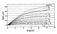
図6に、室温下で測定したMISFET素子の電流−電圧特性を示す。
(Characteristic evaluation of MISFET device)
FIG. 6 shows current-voltage characteristics of the MISFET element measured at room temperature.
ドレイン電圧VDSの増加に伴い、ドレイン電流IDSが増加したことからチャネルがn型半導体であることが分かる。 As the drain voltage V DS increases, the drain current I DS increases, which indicates that the channel is an n-type semiconductor.
これは、アモルファスIn−Ga−Zn−O系半導体がn型であるということ矛盾しない。 This is consistent with the fact that the amorphous In—Ga—Zn—O-based semiconductor is n-type.
IDSはVDS=6V程度で飽和(ピンチオフ)する典型的な半導体トランジスタの挙動を示した。 I DS shows the behavior of a typical semiconductor transistor that saturates (pinch off) at about V DS = 6V.
利得特性を調べたところ、VDS=4V印加時におけるゲート電圧VGSの閾値は約−0.5Vであった。 When the gain characteristics were examined, the threshold value of the gate voltage V GS when V DS = 4 V was applied was about −0.5V.
また、VG=10V時には、IDS=3.1×10⁻⁵Aの電流が流れた。 When V G = 10 V, a current of I DS = 3.1 × 10 −5 A flowed.
これはゲートバイアスにより絶縁体のIn−Ga−Zn−O系アモルファス半導体薄膜内にキャリアを誘起できたことに対応する。トランジスタのオン・オフ比は、103超であった。 This corresponds to the fact that carriers can be induced in the insulator In—Ga—Zn—O-based amorphous semiconductor thin film by the gate bias. The on / off ratio of the transistor was more than 10 3 .
また、出力特性から電界効果移動度を算出したところ、飽和領域において約6.5cm2(Vs)-1の電界効果移動度が得られた。 Further, when the field effect mobility was calculated from the output characteristics, a field effect mobility of about 6.5 cm 2 (Vs) −1 was obtained in the saturation region.
作製した素子に可視光を照射して同様の測定を行ったが、トランジスタ特性の変化は認められなかった。 A similar measurement was performed by irradiating the fabricated device with visible light, but no change in transistor characteristics was observed.
このことから、トランジスタ領域を光から遮断する必要がなく、ボトムエミッションタイプでも開口部として利用できることが分かる。 This indicates that the transistor region does not need to be shielded from light and can be used as an opening even in the bottom emission type.
上記方法とほぼ同じ方法でMISFET素子を形成する。 A MISFET element is formed by substantially the same method as described above.
ただし、電極及び画素部の走査線は全て所望のパルスレーザー堆積法により透明電極(ここではITO使用)を使用し、電極端部は本発明のテーパー形状を形成できるよう、フォトリゾグラフィー法のレジスト条件及びリフトオフ条件を使用した。 However, all the scanning lines of the electrode and the pixel portion use a transparent electrode (in this case, ITO is used) by a desired pulse laser deposition method, and the end portion of the electrode is a resist of the photolithographic method so that the tapered shape of the present invention can be formed. Conditions and lift-off conditions were used.
また、絶縁層は、駆動トランジスタ部のゲート絶縁層と保持容量部の絶縁層を兼用してもよく、又は所望の異なる絶縁層を用いてもよい。本実施例では、同一の絶縁層を用いた。 In addition, the gate insulating layer of the drive transistor portion and the insulating layer of the storage capacitor portion may be used as the insulating layer, or different insulating layers may be used as desired. In this example, the same insulating layer was used.
また、MISFET素子形成した後、平坦化膜をパルスレーザー堆積法により400nm成膜する。この際、ドレイン端子と下部電極を接合させるためのコンタクトホールを形成しておく。 Further, after forming the MISFET element, a flattening film is formed to 400 nm by a pulse laser deposition method. At this time, a contact hole for joining the drain terminal and the lower electrode is formed.
次に再び、パルスレーザー堆積法により透明電極(ここではITO使用)を420nm形成し、下部電極とする。 Next, again, a transparent electrode (in this case, using ITO) is formed with a thickness of 420 nm by a pulse laser deposition method to form a lower electrode.
この下部電極はコンタクトホールを介してドレイン電極と接続されている。 This lower electrode is connected to the drain electrode through a contact hole.
次に、抵抗蒸発法によりホール注入層として4,4’−ビス[N,N−ジアミノ]−4”−フェニルートリフェニルアミンを55nm成膜する。 Next, 55 nm of 4,4'-bis [N, N-diamino] -4 "-phenyl-triphenylamine is formed as a hole injection layer by resistance evaporation.
ホール注入層上にホール輸送層である4,4’−ビス[N−(1−ナフチル)−N−フェニルアミノ]ビフェニル膜を20nm成膜する。 A 4,4′-bis [N- (1-naphthyl) -N-phenylamino] biphenyl film, which is a hole transport layer, is formed to a thickness of 20 nm on the hole injection layer.
次に、発光層として4,4’−ビス(2,2−ジフェニルビニル膜を25nm、さらにその上に電子輸送層としてトリス(8−キノリノール)アルミニウム膜を15nm形成して全体で有機EL発光層とする。 Next, a 4,4′-bis (2,2-diphenylvinyl film as a light emitting layer is formed with a thickness of 25 nm, and a tris (8-quinolinol) aluminum film is formed as an electron transport layer thereon with a thickness of 15 nm. And
最後に抵抗加熱蒸着法によりAlとLiの合金を50nm形成し、その上Alを200nm成膜して上部電極とする。 Finally, an alloy of Al and Li is formed to a thickness of 50 nm by resistance heating vapor deposition, and an Al film is formed thereon to form an upper electrode.
上記した素子にプローブを当てて駆動すると、基板下面から、即ちボトムエミッションタイプで青色の発光が得られた。 When driven by applying a probe to the above-described element, blue light emission was obtained from the bottom surface of the substrate, that is, a bottom emission type.
また同様の方法で、複数の画素を有する発光素子を作成し駆動した。 In the same manner, a light emitting element having a plurality of pixels was produced and driven.
高輝度のきれいな青色の発光が得られた。 A clear blue light emission with high brightness was obtained.
次に両面発光タイプの発光素子を作製する例について説明する。 Next, an example of manufacturing a double-sided light emitting element will be described.
上記方法とほぼ同じ方法でMISFET素子を形成する。 A MISFET element is formed by substantially the same method as described above.
ただし上部電極は抵抗加熱蒸着法によりマグネシウム銀合金を6nm形成し、パルスレーザー堆積法により透明電極(ここではITO使用)を20nm形成し、上部透明電極とする。 However, the upper electrode is formed by forming a magnesium silver alloy with a thickness of 6 nm by a resistance heating vapor deposition method, and forming a transparent electrode (using ITO here) with a thickness of 20 nm by a pulse laser deposition method.
全体で両面発光する有機EL発光層とする。 The organic EL light emitting layer emits light on both sides as a whole.
上記した素子にプローブを当てて駆動すると、両面から、即ち高輝度の青色の発光が得られる。 When driven by applying a probe to the above element, blue light emission with high luminance can be obtained from both sides.
[比較例1]
前記実施例1と同様な方法で、複数の画素を有する発光素子を、本発明の一つである電極端部のテーパー形状をあえて形成しない方法で作成した。
[Comparative Example 1]
In the same manner as in Example 1, a light emitting element having a plurality of pixels was formed by a method that does not dare to form the tapered shape of the electrode end, which is one aspect of the present invention.
ゲート電極とドレイン電極、ソース電極がほぼリーク状態になり、ON状態となり有機層は発光しつづけ、OFF状態にできない部分が数箇所あり、画質としては、実施例1に比べ若干劣っていた。 The gate electrode, the drain electrode, and the source electrode were almost leaked, turned ON, the organic layer continued to emit light, and there were several portions that could not be turned OFF. The image quality was slightly inferior to that of Example 1.
また、上記の説明では、In−Ga−Znを含み構成される。 In the above description, In—Ga—Zn is included.
本発明に係る発光素子は、プラスチックフィルムをはじめとするフレキシブル素材に半導体の薄膜を形成し、フレキシブル・ディスプレイをはじめ、ICカードやIDタグなどに幅広く応用できる。 The light emitting device according to the present invention can be widely applied to a flexible display, an IC card, an ID tag, and the like by forming a semiconductor thin film on a flexible material such as a plastic film.
700 基板
701 半導体層(活性層)
702 第一透明電極
703 絶縁層
704 第二透明電極
705 駆動トランジスタ
706 保持容量
707 走査線
708 平坦化膜
709 下部透明電極
710 素子分離膜
711 有機層(有機EL層)
712 ホール輸送層
713 発光層
714 電子輸送層
715 上部電極
716 第三透明電極
717 カバーガラス
718 スイッチングトランジスタ
719 半導体層
720 第4透明電極
721 第5透明電極
722 第6透明電極
723 保護層
81 トランジスタ1
82 トランジスタ2
83 コンデンサー(保持容量)
84 有機層(有機EL層)
85 走査電極線
86 信号電極線
87 共通電極線
901 駆動トランジスタ
902 スイッチングトランジスタ
903 保持容量
904 共通電極線
905 走査線
906 信号線
700
702 First
712
82
83 Condenser (holding capacity)
84 Organic layer (organic EL layer)
85 Scan electrode line 86 Signal electrode line 87 Common electrode line 901 Drive transistor 902 Switching transistor 903 Retention capacity 904 Common electrode line 905 Scan line 906 Signal line
Claims (11)
前記薄膜トランジスタの活性層がInとGaとZnを含む非晶質の酸化物からなり、
前記非晶質酸化物は、電子キャリア濃度が10 18 /cm 3 未満であり、かつ電子数の増加とともに、電子移動度が大きくなる特性を有しており、
前記薄膜トランジスタは、ゲート電圧無印加時のドレイン・ソース端子間の電流が10マイクロアンペア未満であり、
前記ドレイン電極に前記発光層の一部が電気的に接続され、
少なくとも前記ソース、ドレイン及びゲート電極と、前記第1の電極と、前記第1の電極と前記ドレイン電極とを接続する電極と、前記保持容量と、前記スイッチングトランジスタのソース、ドレイン及びゲート電極と、が透明であることを特徴とする発光素子。 Includes a source electrode, a drain electrode, a gate electrode, a thin film transistor; and a clamping or light emitting layer between the first electrode and the second electrode to be driven by the thin film transistor, a storage capacitor, a switching transistor, the In the light emitting element,
Active layer of the thin film transistor is an oxide of amorphous containing In, Ga, and Zn, and
The amorphous oxide has a characteristic that the electron carrier concentration is less than 10 18 / cm 3 and the electron mobility increases as the number of electrons increases.
In the thin film transistor, the current between the drain and source terminals when no gate voltage is applied is less than 10 microamperes,
Some of the light-emitting layer is electrically connected to the drain electrode,
At least before Kiso over scan, a drain, and a gate electrode, the first electrode, the electrode of the first electrode connecting the drain electrode, the storage capacitor, the source of the switching transistor, the drain and gate A light-emitting element , wherein the electrode is transparent.
Priority Applications (1)
| Application Number | Priority Date | Filing Date | Title |
|---|---|---|---|
| JP2005258265A JP4732080B2 (en) | 2005-09-06 | 2005-09-06 | Light emitting element |
Applications Claiming Priority (1)
| Application Number | Priority Date | Filing Date | Title |
|---|---|---|---|
| JP2005258265A JP4732080B2 (en) | 2005-09-06 | 2005-09-06 | Light emitting element |
Publications (2)
| Publication Number | Publication Date |
|---|---|
| JP2007073311A JP2007073311A (en) | 2007-03-22 |
| JP4732080B2 true JP4732080B2 (en) | 2011-07-27 |
Family
ID=37934602
Family Applications (1)
| Application Number | Title | Priority Date | Filing Date |
|---|---|---|---|
| JP2005258265A Expired - Fee Related JP4732080B2 (en) | 2005-09-06 | 2005-09-06 | Light emitting element |
Country Status (1)
| Country | Link |
|---|---|
| JP (1) | JP4732080B2 (en) |
Families Citing this family (20)
| Publication number | Priority date | Publication date | Assignee | Title |
|---|---|---|---|---|
| JP2007286150A (en) * | 2006-04-13 | 2007-11-01 | Idemitsu Kosan Co Ltd | Electrooptical device, and tft substrate for controlling electric current and method of manufacturing the same |
| JP5105842B2 (en) * | 2006-12-05 | 2012-12-26 | キヤノン株式会社 | Display device using oxide semiconductor and manufacturing method thereof |
| JP2009194351A (en) | 2007-04-27 | 2009-08-27 | Canon Inc | Thin film transistor and its manufacturing method |
| JP2008300612A (en) * | 2007-05-31 | 2008-12-11 | Panasonic Corp | Display device and manufacturing method thereof |
| KR101392276B1 (en) | 2007-10-31 | 2014-05-07 | 삼성디스플레이 주식회사 | Thin film transistor substrate and method of manufacturing the same |
| JP5191247B2 (en) * | 2008-02-06 | 2013-05-08 | 富士フイルム株式会社 | Thin film field effect transistor and display device using the same |
| TWI491048B (en) * | 2008-07-31 | 2015-07-01 | Semiconductor Energy Lab | Semiconductor device |
| WO2010018875A1 (en) * | 2008-08-15 | 2010-02-18 | 株式会社アルバック | Process for producing field effect transistor |
| TWI478356B (en) | 2008-10-31 | 2015-03-21 | Semiconductor Energy Lab | Semiconductor device and method for manufacturing the same |
| US8461582B2 (en) | 2009-03-05 | 2013-06-11 | Semiconductor Energy Laboratory Co., Ltd. | Semiconductor device and method for manufacturing the same |
| TWI830077B (en) * | 2009-08-07 | 2024-01-21 | 日商半導體能源研究所股份有限公司 | Semiconductor device |
| WO2011027701A1 (en) * | 2009-09-04 | 2011-03-10 | Semiconductor Energy Laboratory Co., Ltd. | Light-emitting device and method for manufacturing the same |
| KR102377866B1 (en) * | 2009-10-21 | 2022-03-22 | 가부시키가이샤 한도오따이 에네루기 켄큐쇼 | Analog circuit and semiconductor device |
| KR101750982B1 (en) | 2009-11-06 | 2017-06-26 | 가부시키가이샤 한도오따이 에네루기 켄큐쇼 | Semiconductor device and manufacturing method thereof |
| WO2011068028A1 (en) * | 2009-12-04 | 2011-06-09 | Semiconductor Energy Laboratory Co., Ltd. | Semiconductor element, semiconductor device, and method for manufacturing the same |
| US8780629B2 (en) | 2010-01-15 | 2014-07-15 | Semiconductor Energy Laboratory Co., Ltd. | Semiconductor device and driving method thereof |
| JP5627929B2 (en) * | 2010-05-28 | 2014-11-19 | 富士フイルム株式会社 | Method for manufacturing amorphous oxide thin film and method for manufacturing field effect transistor |
| US8907392B2 (en) * | 2011-12-22 | 2014-12-09 | Semiconductor Energy Laboratory Co., Ltd. | Semiconductor memory device including stacked sub memory cells |
| JP5971849B2 (en) * | 2012-07-11 | 2016-08-17 | パナソニック液晶ディスプレイ株式会社 | Display device and pixel defect correcting method |
| KR101471149B1 (en) * | 2013-11-12 | 2014-12-11 | 삼성디스플레이 주식회사 | Thin film transistor substrate and method of manufacturing the same |
Citations (5)
| Publication number | Priority date | Publication date | Assignee | Title |
|---|---|---|---|---|
| JP2000150900A (en) * | 1998-11-17 | 2000-05-30 | Japan Science & Technology Corp | Transistor and semiconductor device |
| JP2002076356A (en) * | 2000-09-01 | 2002-03-15 | Japan Science & Technology Corp | Semiconductor device |
| JP2002289859A (en) * | 2001-03-23 | 2002-10-04 | Minolta Co Ltd | Thin-film transistor |
| JP2004103957A (en) * | 2002-09-11 | 2004-04-02 | Japan Science & Technology Corp | Transparent thin film field effect type transistor using homologous thin film as active layer |
| JP2006186319A (en) * | 2004-11-10 | 2006-07-13 | Canon Inc | Light emitting device and indicating device |
-
2005
- 2005-09-06 JP JP2005258265A patent/JP4732080B2/en not_active Expired - Fee Related
Patent Citations (5)
| Publication number | Priority date | Publication date | Assignee | Title |
|---|---|---|---|---|
| JP2000150900A (en) * | 1998-11-17 | 2000-05-30 | Japan Science & Technology Corp | Transistor and semiconductor device |
| JP2002076356A (en) * | 2000-09-01 | 2002-03-15 | Japan Science & Technology Corp | Semiconductor device |
| JP2002289859A (en) * | 2001-03-23 | 2002-10-04 | Minolta Co Ltd | Thin-film transistor |
| JP2004103957A (en) * | 2002-09-11 | 2004-04-02 | Japan Science & Technology Corp | Transparent thin film field effect type transistor using homologous thin film as active layer |
| JP2006186319A (en) * | 2004-11-10 | 2006-07-13 | Canon Inc | Light emitting device and indicating device |
Also Published As
| Publication number | Publication date |
|---|---|
| JP2007073311A (en) | 2007-03-22 |
Similar Documents
| Publication | Publication Date | Title |
|---|---|---|
| JP4732080B2 (en) | Light emitting element | |
| JP5016831B2 (en) | LIGHT EMITTING ELEMENT USING OXIDE SEMICONDUCTOR THIN FILM TRANSISTOR AND IMAGE DISPLAY DEVICE USING THE SAME | |
| US10714627B2 (en) | Bottom gate type thin film transistor, method of manufacturing the same, and display apparatus | |
| JP5105842B2 (en) | Display device using oxide semiconductor and manufacturing method thereof | |
| KR100953596B1 (en) | Light-emitting device | |
| EP1984954B1 (en) | Field effect transistor using oxide film for channel and method of manufacturing the same | |
| JP5224676B2 (en) | Manufacturing method of display device | |
| JP5553868B2 (en) | Display device using oxide semiconductor and manufacturing method thereof | |
| TW202317788A (en) | Oxide semiconductor sputtering target and method of fabricating thin-film transistor using same |
Legal Events
| Date | Code | Title | Description |
|---|---|---|---|
| RD04 | Notification of resignation of power of attorney |
Free format text: JAPANESE INTERMEDIATE CODE: A7424 Effective date: 20080207 |
|
| A621 | Written request for application examination |
Free format text: JAPANESE INTERMEDIATE CODE: A621 Effective date: 20080905 |
|
| RD01 | Notification of change of attorney |
Free format text: JAPANESE INTERMEDIATE CODE: A7421 Effective date: 20090324 |
|
| RD04 | Notification of resignation of power of attorney |
Free format text: JAPANESE INTERMEDIATE CODE: A7424 Effective date: 20100201 |
|
| RD01 | Notification of change of attorney |
Free format text: JAPANESE INTERMEDIATE CODE: A7421 Effective date: 20100630 |
|
| A977 | Report on retrieval |
Free format text: JAPANESE INTERMEDIATE CODE: A971007 Effective date: 20101014 |
|
| A131 | Notification of reasons for refusal |
Free format text: JAPANESE INTERMEDIATE CODE: A131 Effective date: 20101116 |
|
| A521 | Request for written amendment filed |
Free format text: JAPANESE INTERMEDIATE CODE: A523 Effective date: 20110117 |
|
| TRDD | Decision of grant or rejection written | ||
| A01 | Written decision to grant a patent or to grant a registration (utility model) |
Free format text: JAPANESE INTERMEDIATE CODE: A01 Effective date: 20110419 |
|
| A01 | Written decision to grant a patent or to grant a registration (utility model) |
Free format text: JAPANESE INTERMEDIATE CODE: A01 |
|
| A61 | First payment of annual fees (during grant procedure) |
Free format text: JAPANESE INTERMEDIATE CODE: A61 Effective date: 20110420 |
|
| FPAY | Renewal fee payment (event date is renewal date of database) |
Free format text: PAYMENT UNTIL: 20140428 Year of fee payment: 3 |
|
| R150 | Certificate of patent or registration of utility model |
Ref document number: 4732080 Country of ref document: JP Free format text: JAPANESE INTERMEDIATE CODE: R150 Free format text: JAPANESE INTERMEDIATE CODE: R150 |
|
| LAPS | Cancellation because of no payment of annual fees |