JP5883699B2 - Programmable LSI - Google Patents
Programmable LSI Download PDFInfo
- Publication number
- JP5883699B2 JP5883699B2 JP2012075636A JP2012075636A JP5883699B2 JP 5883699 B2 JP5883699 B2 JP 5883699B2 JP 2012075636 A JP2012075636 A JP 2012075636A JP 2012075636 A JP2012075636 A JP 2012075636A JP 5883699 B2 JP5883699 B2 JP 5883699B2
- Authority
- JP
- Japan
- Prior art keywords
- circuit
- memory
- transistor
- data
- memory cell
- Prior art date
- Legal status (The legal status is an assumption and is not a legal conclusion. Google has not performed a legal analysis and makes no representation as to the accuracy of the status listed.)
- Expired - Fee Related
Links
- 230000015654 memory Effects 0.000 claims description 631
- 239000004065 semiconductor Substances 0.000 claims description 256
- 239000003990 capacitor Substances 0.000 claims description 57
- 238000003860 storage Methods 0.000 claims description 30
- 230000006870 function Effects 0.000 claims description 27
- 229910052710 silicon Inorganic materials 0.000 claims description 19
- 239000010703 silicon Substances 0.000 claims description 19
- 238000012545 processing Methods 0.000 claims description 18
- 239000010408 film Substances 0.000 description 299
- 239000010410 layer Substances 0.000 description 244
- 238000000034 method Methods 0.000 description 93
- 229910052760 oxygen Inorganic materials 0.000 description 54
- QVGXLLKOCUKJST-UHFFFAOYSA-N atomic oxygen Chemical compound [O] QVGXLLKOCUKJST-UHFFFAOYSA-N 0.000 description 53
- 239000001301 oxygen Substances 0.000 description 53
- 238000010438 heat treatment Methods 0.000 description 44
- 239000000758 substrate Substances 0.000 description 44
- 239000012535 impurity Substances 0.000 description 33
- IJGRMHOSHXDMSA-UHFFFAOYSA-N Atomic nitrogen Chemical compound N#N IJGRMHOSHXDMSA-UHFFFAOYSA-N 0.000 description 32
- 230000015572 biosynthetic process Effects 0.000 description 31
- 239000000463 material Substances 0.000 description 30
- 239000007789 gas Substances 0.000 description 28
- 239000000872 buffer Substances 0.000 description 25
- 239000013078 crystal Substances 0.000 description 25
- 239000001257 hydrogen Substances 0.000 description 24
- 229910052739 hydrogen Inorganic materials 0.000 description 24
- 238000005530 etching Methods 0.000 description 23
- 239000000203 mixture Substances 0.000 description 23
- XKRFYHLGVUSROY-UHFFFAOYSA-N Argon Chemical compound [Ar] XKRFYHLGVUSROY-UHFFFAOYSA-N 0.000 description 22
- UFHFLCQGNIYNRP-UHFFFAOYSA-N Hydrogen Chemical compound [H][H] UFHFLCQGNIYNRP-UHFFFAOYSA-N 0.000 description 21
- 238000010586 diagram Methods 0.000 description 20
- 239000010936 titanium Substances 0.000 description 20
- 229910052782 aluminium Inorganic materials 0.000 description 19
- 238000004544 sputter deposition Methods 0.000 description 19
- 229910052719 titanium Inorganic materials 0.000 description 19
- XUIMIQQOPSSXEZ-UHFFFAOYSA-N Silicon Chemical compound [Si] XUIMIQQOPSSXEZ-UHFFFAOYSA-N 0.000 description 18
- RTAQQCXQSZGOHL-UHFFFAOYSA-N Titanium Chemical compound [Ti] RTAQQCXQSZGOHL-UHFFFAOYSA-N 0.000 description 17
- XAGFODPZIPBFFR-UHFFFAOYSA-N aluminium Chemical compound [Al] XAGFODPZIPBFFR-UHFFFAOYSA-N 0.000 description 17
- 229910052733 gallium Inorganic materials 0.000 description 17
- 229910001195 gallium oxide Inorganic materials 0.000 description 17
- 229910052757 nitrogen Inorganic materials 0.000 description 17
- XLOMVQKBTHCTTD-UHFFFAOYSA-N Zinc monoxide Chemical compound [Zn]=O XLOMVQKBTHCTTD-UHFFFAOYSA-N 0.000 description 16
- 239000012298 atmosphere Substances 0.000 description 16
- 229910007541 Zn O Inorganic materials 0.000 description 15
- 230000008569 process Effects 0.000 description 15
- 239000011701 zinc Substances 0.000 description 15
- 229910052751 metal Inorganic materials 0.000 description 14
- 239000002184 metal Substances 0.000 description 13
- TWNQGVIAIRXVLR-UHFFFAOYSA-N oxo(oxoalumanyloxy)alumane Chemical compound O=[Al]O[Al]=O TWNQGVIAIRXVLR-UHFFFAOYSA-N 0.000 description 13
- AJNVQOSZGJRYEI-UHFFFAOYSA-N digallium;oxygen(2-) Chemical compound [O-2].[O-2].[O-2].[Ga+3].[Ga+3] AJNVQOSZGJRYEI-UHFFFAOYSA-N 0.000 description 12
- 238000004519 manufacturing process Methods 0.000 description 12
- GYHNNYVSQQEPJS-UHFFFAOYSA-N Gallium Chemical compound [Ga] GYHNNYVSQQEPJS-UHFFFAOYSA-N 0.000 description 11
- 229910052786 argon Inorganic materials 0.000 description 11
- 239000002019 doping agent Substances 0.000 description 10
- VYPSYNLAJGMNEJ-UHFFFAOYSA-N silicon dioxide Inorganic materials O=[Si]=O VYPSYNLAJGMNEJ-UHFFFAOYSA-N 0.000 description 10
- 229910052721 tungsten Inorganic materials 0.000 description 10
- 239000010937 tungsten Substances 0.000 description 10
- 229910052581 Si3N4 Inorganic materials 0.000 description 9
- 239000000460 chlorine Substances 0.000 description 9
- 229910052750 molybdenum Inorganic materials 0.000 description 9
- HQVNEWCFYHHQES-UHFFFAOYSA-N silicon nitride Chemical compound N12[Si]34N5[Si]62N3[Si]51N64 HQVNEWCFYHHQES-UHFFFAOYSA-N 0.000 description 9
- WFKWXMTUELFFGS-UHFFFAOYSA-N tungsten Chemical compound [W] WFKWXMTUELFFGS-UHFFFAOYSA-N 0.000 description 9
- XLYOFNOQVPJJNP-UHFFFAOYSA-N water Substances O XLYOFNOQVPJJNP-UHFFFAOYSA-N 0.000 description 9
- 239000010949 copper Substances 0.000 description 8
- 238000002425 crystallisation Methods 0.000 description 8
- 239000011733 molybdenum Substances 0.000 description 8
- 229910052814 silicon oxide Inorganic materials 0.000 description 8
- 239000011787 zinc oxide Substances 0.000 description 8
- ZAMOUSCENKQFHK-UHFFFAOYSA-N Chlorine atom Chemical compound [Cl] ZAMOUSCENKQFHK-UHFFFAOYSA-N 0.000 description 7
- ZOKXTWBITQBERF-UHFFFAOYSA-N Molybdenum Chemical compound [Mo] ZOKXTWBITQBERF-UHFFFAOYSA-N 0.000 description 7
- 229910052783 alkali metal Inorganic materials 0.000 description 7
- 150000001340 alkali metals Chemical class 0.000 description 7
- 230000004888 barrier function Effects 0.000 description 7
- 229910052801 chlorine Inorganic materials 0.000 description 7
- 239000011810 insulating material Substances 0.000 description 7
- 239000011159 matrix material Substances 0.000 description 7
- 239000002356 single layer Substances 0.000 description 7
- 239000011734 sodium Substances 0.000 description 7
- 229910052715 tantalum Inorganic materials 0.000 description 7
- GUVRBAGPIYLISA-UHFFFAOYSA-N tantalum atom Chemical compound [Ta] GUVRBAGPIYLISA-UHFFFAOYSA-N 0.000 description 7
- 229910052725 zinc Inorganic materials 0.000 description 7
- RYGMFSIKBFXOCR-UHFFFAOYSA-N Copper Chemical compound [Cu] RYGMFSIKBFXOCR-UHFFFAOYSA-N 0.000 description 6
- 229910045601 alloy Inorganic materials 0.000 description 6
- 239000000956 alloy Substances 0.000 description 6
- 229910052795 boron group element Inorganic materials 0.000 description 6
- 239000011651 chromium Substances 0.000 description 6
- 229910052802 copper Inorganic materials 0.000 description 6
- 238000013500 data storage Methods 0.000 description 6
- 229910052734 helium Inorganic materials 0.000 description 6
- 239000001307 helium Substances 0.000 description 6
- SWQJXJOGLNCZEY-UHFFFAOYSA-N helium atom Chemical compound [He] SWQJXJOGLNCZEY-UHFFFAOYSA-N 0.000 description 6
- 238000004151 rapid thermal annealing Methods 0.000 description 6
- VYZAMTAEIAYCRO-UHFFFAOYSA-N Chromium Chemical compound [Cr] VYZAMTAEIAYCRO-UHFFFAOYSA-N 0.000 description 5
- RNQKDQAVIXDKAG-UHFFFAOYSA-N aluminum gallium Chemical compound [Al].[Ga] RNQKDQAVIXDKAG-UHFFFAOYSA-N 0.000 description 5
- 229910052804 chromium Inorganic materials 0.000 description 5
- 230000006378 damage Effects 0.000 description 5
- 238000001312 dry etching Methods 0.000 description 5
- 229910052738 indium Inorganic materials 0.000 description 5
- 229910044991 metal oxide Inorganic materials 0.000 description 5
- 150000004706 metal oxides Chemical class 0.000 description 5
- 238000005240 physical vapour deposition Methods 0.000 description 5
- 238000009832 plasma treatment Methods 0.000 description 5
- 239000010409 thin film Substances 0.000 description 5
- QGZKDVFQNNGYKY-UHFFFAOYSA-N Ammonia Chemical compound N QGZKDVFQNNGYKY-UHFFFAOYSA-N 0.000 description 4
- 239000012300 argon atmosphere Substances 0.000 description 4
- 125000004429 atom Chemical group 0.000 description 4
- 150000001875 compounds Chemical class 0.000 description 4
- 239000000470 constituent Substances 0.000 description 4
- PMHQVHHXPFUNSP-UHFFFAOYSA-M copper(1+);methylsulfanylmethane;bromide Chemical compound Br[Cu].CSC PMHQVHHXPFUNSP-UHFFFAOYSA-M 0.000 description 4
- 239000011521 glass Substances 0.000 description 4
- -1 hafnium aluminate Chemical class 0.000 description 4
- 150000002431 hydrogen Chemical class 0.000 description 4
- 125000004435 hydrogen atom Chemical group [H]* 0.000 description 4
- 125000002887 hydroxy group Chemical group [H]O* 0.000 description 4
- 238000009616 inductively coupled plasma Methods 0.000 description 4
- 230000003071 parasitic effect Effects 0.000 description 4
- 239000000126 substance Substances 0.000 description 4
- VZGDMQKNWNREIO-UHFFFAOYSA-N tetrachloromethane Chemical compound ClC(Cl)(Cl)Cl VZGDMQKNWNREIO-UHFFFAOYSA-N 0.000 description 4
- 229910052984 zinc sulfide Inorganic materials 0.000 description 4
- QTBSBXVTEAMEQO-UHFFFAOYSA-N Acetic acid Chemical compound CC(O)=O QTBSBXVTEAMEQO-UHFFFAOYSA-N 0.000 description 3
- 101100191136 Arabidopsis thaliana PCMP-A2 gene Proteins 0.000 description 3
- MYMOFIZGZYHOMD-UHFFFAOYSA-N Dioxygen Chemical compound O=O MYMOFIZGZYHOMD-UHFFFAOYSA-N 0.000 description 3
- YCKRFDGAMUMZLT-UHFFFAOYSA-N Fluorine atom Chemical compound [F] YCKRFDGAMUMZLT-UHFFFAOYSA-N 0.000 description 3
- DGAQECJNVWCQMB-PUAWFVPOSA-M Ilexoside XXIX Chemical compound C[C@@H]1CC[C@@]2(CC[C@@]3(C(=CC[C@H]4[C@]3(CC[C@@H]5[C@@]4(CC[C@@H](C5(C)C)OS(=O)(=O)[O-])C)C)[C@@H]2[C@]1(C)O)C)C(=O)O[C@H]6[C@@H]([C@H]([C@@H]([C@H](O6)CO)O)O)O.[Na+] DGAQECJNVWCQMB-PUAWFVPOSA-M 0.000 description 3
- MUBZPKHOEPUJKR-UHFFFAOYSA-N Oxalic acid Chemical compound OC(=O)C(O)=O MUBZPKHOEPUJKR-UHFFFAOYSA-N 0.000 description 3
- OAICVXFJPJFONN-UHFFFAOYSA-N Phosphorus Chemical compound [P] OAICVXFJPJFONN-UHFFFAOYSA-N 0.000 description 3
- 101100422768 Saccharomyces cerevisiae (strain ATCC 204508 / S288c) SUL2 gene Proteins 0.000 description 3
- 101100048260 Saccharomyces cerevisiae (strain ATCC 204508 / S288c) UBX2 gene Proteins 0.000 description 3
- HCHKCACWOHOZIP-UHFFFAOYSA-N Zinc Chemical compound [Zn] HCHKCACWOHOZIP-UHFFFAOYSA-N 0.000 description 3
- 230000009471 action Effects 0.000 description 3
- 230000003197 catalytic effect Effects 0.000 description 3
- 238000005229 chemical vapour deposition Methods 0.000 description 3
- KRKNYBCHXYNGOX-UHFFFAOYSA-N citric acid Chemical compound OC(=O)CC(O)(C(O)=O)CC(O)=O KRKNYBCHXYNGOX-UHFFFAOYSA-N 0.000 description 3
- 229910001882 dioxygen Inorganic materials 0.000 description 3
- 230000000694 effects Effects 0.000 description 3
- 229910052731 fluorine Inorganic materials 0.000 description 3
- 239000011737 fluorine Substances 0.000 description 3
- 229910052735 hafnium Inorganic materials 0.000 description 3
- 150000004678 hydrides Chemical class 0.000 description 3
- 229910003437 indium oxide Inorganic materials 0.000 description 3
- PJXISJQVUVHSOJ-UHFFFAOYSA-N indium(iii) oxide Chemical compound [O-2].[O-2].[O-2].[In+3].[In+3] PJXISJQVUVHSOJ-UHFFFAOYSA-N 0.000 description 3
- 238000005468 ion implantation Methods 0.000 description 3
- 238000010884 ion-beam technique Methods 0.000 description 3
- 150000002500 ions Chemical class 0.000 description 3
- 230000014759 maintenance of location Effects 0.000 description 3
- 125000004433 nitrogen atom Chemical group N* 0.000 description 3
- 229910052698 phosphorus Inorganic materials 0.000 description 3
- 239000011574 phosphorus Substances 0.000 description 3
- 230000000717 retained effect Effects 0.000 description 3
- 230000002441 reversible effect Effects 0.000 description 3
- 229910052708 sodium Inorganic materials 0.000 description 3
- TXEYQDLBPFQVAA-UHFFFAOYSA-N tetrafluoromethane Chemical compound FC(F)(F)F TXEYQDLBPFQVAA-UHFFFAOYSA-N 0.000 description 3
- FAQYAMRNWDIXMY-UHFFFAOYSA-N trichloroborane Chemical compound ClB(Cl)Cl FAQYAMRNWDIXMY-UHFFFAOYSA-N 0.000 description 3
- ZOXJGFHDIHLPTG-UHFFFAOYSA-N Boron Chemical compound [B] ZOXJGFHDIHLPTG-UHFFFAOYSA-N 0.000 description 2
- XPDWGBQVDMORPB-UHFFFAOYSA-N Fluoroform Chemical compound FC(F)F XPDWGBQVDMORPB-UHFFFAOYSA-N 0.000 description 2
- MHAJPDPJQMAIIY-UHFFFAOYSA-N Hydrogen peroxide Chemical compound OO MHAJPDPJQMAIIY-UHFFFAOYSA-N 0.000 description 2
- 229910003023 Mg-Al Inorganic materials 0.000 description 2
- 229910019092 Mg-O Inorganic materials 0.000 description 2
- 229910019395 Mg—O Inorganic materials 0.000 description 2
- 229910052779 Neodymium Inorganic materials 0.000 description 2
- GQPLMRYTRLFLPF-UHFFFAOYSA-N Nitrous Oxide Chemical compound [O-][N+]#N GQPLMRYTRLFLPF-UHFFFAOYSA-N 0.000 description 2
- BPQQTUXANYXVAA-UHFFFAOYSA-N Orthosilicate Chemical compound [O-][Si]([O-])([O-])[O-] BPQQTUXANYXVAA-UHFFFAOYSA-N 0.000 description 2
- NBIIXXVUZAFLBC-UHFFFAOYSA-N Phosphoric acid Chemical compound OP(O)(O)=O NBIIXXVUZAFLBC-UHFFFAOYSA-N 0.000 description 2
- 229910001069 Ti alloy Inorganic materials 0.000 description 2
- 229910000611 Zinc aluminium Inorganic materials 0.000 description 2
- HXFVOUUOTHJFPX-UHFFFAOYSA-N alumane;zinc Chemical compound [AlH3].[Zn] HXFVOUUOTHJFPX-UHFFFAOYSA-N 0.000 description 2
- JYMITAMFTJDTAE-UHFFFAOYSA-N aluminum zinc oxygen(2-) Chemical compound [O-2].[Al+3].[Zn+2] JYMITAMFTJDTAE-UHFFFAOYSA-N 0.000 description 2
- 229910021529 ammonia Inorganic materials 0.000 description 2
- 229910052785 arsenic Inorganic materials 0.000 description 2
- RQNWIZPPADIBDY-UHFFFAOYSA-N arsenic atom Chemical compound [As] RQNWIZPPADIBDY-UHFFFAOYSA-N 0.000 description 2
- 229910052796 boron Inorganic materials 0.000 description 2
- 229910052799 carbon Inorganic materials 0.000 description 2
- 230000018044 dehydration Effects 0.000 description 2
- 238000006297 dehydration reaction Methods 0.000 description 2
- 238000006356 dehydrogenation reaction Methods 0.000 description 2
- 238000011161 development Methods 0.000 description 2
- 239000000428 dust Substances 0.000 description 2
- 238000011049 filling Methods 0.000 description 2
- VBJZVLUMGGDVMO-UHFFFAOYSA-N hafnium atom Chemical compound [Hf] VBJZVLUMGGDVMO-UHFFFAOYSA-N 0.000 description 2
- 229910000449 hafnium oxide Inorganic materials 0.000 description 2
- WIHZLLGSGQNAGK-UHFFFAOYSA-N hafnium(4+);oxygen(2-) Chemical compound [O-2].[O-2].[Hf+4] WIHZLLGSGQNAGK-UHFFFAOYSA-N 0.000 description 2
- APFVFJFRJDLVQX-UHFFFAOYSA-N indium atom Chemical compound [In] APFVFJFRJDLVQX-UHFFFAOYSA-N 0.000 description 2
- AMGQUBHHOARCQH-UHFFFAOYSA-N indium;oxotin Chemical compound [In].[Sn]=O AMGQUBHHOARCQH-UHFFFAOYSA-N 0.000 description 2
- 239000011261 inert gas Substances 0.000 description 2
- 238000005499 laser crystallization Methods 0.000 description 2
- 239000000696 magnetic material Substances 0.000 description 2
- 229910052748 manganese Inorganic materials 0.000 description 2
- 239000011572 manganese Substances 0.000 description 2
- QEFYFXOXNSNQGX-UHFFFAOYSA-N neodymium atom Chemical compound [Nd] QEFYFXOXNSNQGX-UHFFFAOYSA-N 0.000 description 2
- 229910052754 neon Inorganic materials 0.000 description 2
- GKAOGPIIYCISHV-UHFFFAOYSA-N neon atom Chemical compound [Ne] GKAOGPIIYCISHV-UHFFFAOYSA-N 0.000 description 2
- 239000010955 niobium Substances 0.000 description 2
- 150000004767 nitrides Chemical class 0.000 description 2
- 238000000206 photolithography Methods 0.000 description 2
- 238000005268 plasma chemical vapour deposition Methods 0.000 description 2
- 238000001020 plasma etching Methods 0.000 description 2
- 239000010453 quartz Substances 0.000 description 2
- 230000005855 radiation Effects 0.000 description 2
- 230000009467 reduction Effects 0.000 description 2
- 239000003870 refractory metal Substances 0.000 description 2
- 229910052706 scandium Inorganic materials 0.000 description 2
- SIXSYDAISGFNSX-UHFFFAOYSA-N scandium atom Chemical compound [Sc] SIXSYDAISGFNSX-UHFFFAOYSA-N 0.000 description 2
- 230000003068 static effect Effects 0.000 description 2
- SFZCNBIFKDRMGX-UHFFFAOYSA-N sulfur hexafluoride Chemical compound FS(F)(F)(F)(F)F SFZCNBIFKDRMGX-UHFFFAOYSA-N 0.000 description 2
- 229960000909 sulfur hexafluoride Drugs 0.000 description 2
- MZLGASXMSKOWSE-UHFFFAOYSA-N tantalum nitride Chemical compound [Ta]#N MZLGASXMSKOWSE-UHFFFAOYSA-N 0.000 description 2
- 229910052718 tin Inorganic materials 0.000 description 2
- 238000007740 vapor deposition Methods 0.000 description 2
- 238000001039 wet etching Methods 0.000 description 2
- 229910052724 xenon Inorganic materials 0.000 description 2
- FHNFHKCVQCLJFQ-UHFFFAOYSA-N xenon atom Chemical compound [Xe] FHNFHKCVQCLJFQ-UHFFFAOYSA-N 0.000 description 2
- YVTHLONGBIQYBO-UHFFFAOYSA-N zinc indium(3+) oxygen(2-) Chemical compound [O--].[Zn++].[In+3] YVTHLONGBIQYBO-UHFFFAOYSA-N 0.000 description 2
- VXEGSRKPIUDPQT-UHFFFAOYSA-N 4-[4-(4-methoxyphenyl)piperazin-1-yl]aniline Chemical compound C1=CC(OC)=CC=C1N1CCN(C=2C=CC(N)=CC=2)CC1 VXEGSRKPIUDPQT-UHFFFAOYSA-N 0.000 description 1
- VHUUQVKOLVNVRT-UHFFFAOYSA-N Ammonium hydroxide Chemical compound [NH4+].[OH-] VHUUQVKOLVNVRT-UHFFFAOYSA-N 0.000 description 1
- CPELXLSAUQHCOX-UHFFFAOYSA-M Bromide Chemical compound [Br-] CPELXLSAUQHCOX-UHFFFAOYSA-M 0.000 description 1
- OKTJSMMVPCPJKN-UHFFFAOYSA-N Carbon Chemical compound [C] OKTJSMMVPCPJKN-UHFFFAOYSA-N 0.000 description 1
- 229910002601 GaN Inorganic materials 0.000 description 1
- JMASRVWKEDWRBT-UHFFFAOYSA-N Gallium nitride Chemical compound [Ga]#N JMASRVWKEDWRBT-UHFFFAOYSA-N 0.000 description 1
- CPELXLSAUQHCOX-UHFFFAOYSA-N Hydrogen bromide Chemical compound Br CPELXLSAUQHCOX-UHFFFAOYSA-N 0.000 description 1
- 108010083687 Ion Pumps Proteins 0.000 description 1
- WHXSMMKQMYFTQS-UHFFFAOYSA-N Lithium Chemical compound [Li] WHXSMMKQMYFTQS-UHFFFAOYSA-N 0.000 description 1
- FYYHWMGAXLPEAU-UHFFFAOYSA-N Magnesium Chemical compound [Mg] FYYHWMGAXLPEAU-UHFFFAOYSA-N 0.000 description 1
- GRYLNZFGIOXLOG-UHFFFAOYSA-N Nitric acid Chemical compound O[N+]([O-])=O GRYLNZFGIOXLOG-UHFFFAOYSA-N 0.000 description 1
- 238000006124 Pilkington process Methods 0.000 description 1
- ZLMJMSJWJFRBEC-UHFFFAOYSA-N Potassium Chemical compound [K] ZLMJMSJWJFRBEC-UHFFFAOYSA-N 0.000 description 1
- 229910018503 SF6 Inorganic materials 0.000 description 1
- 229910003902 SiCl 4 Inorganic materials 0.000 description 1
- 229910004298 SiO 2 Inorganic materials 0.000 description 1
- 229910020833 Sn-Al-Zn Inorganic materials 0.000 description 1
- 229910020923 Sn-O Inorganic materials 0.000 description 1
- NRTOMJZYCJJWKI-UHFFFAOYSA-N Titanium nitride Chemical compound [Ti]#N NRTOMJZYCJJWKI-UHFFFAOYSA-N 0.000 description 1
- QCWXUUIWCKQGHC-UHFFFAOYSA-N Zirconium Chemical compound [Zr] QCWXUUIWCKQGHC-UHFFFAOYSA-N 0.000 description 1
- 229910009369 Zn Mg Inorganic materials 0.000 description 1
- 229910007573 Zn-Mg Inorganic materials 0.000 description 1
- 230000001133 acceleration Effects 0.000 description 1
- 229910052784 alkaline earth metal Inorganic materials 0.000 description 1
- 150000001342 alkaline earth metals Chemical class 0.000 description 1
- 229910000147 aluminium phosphate Inorganic materials 0.000 description 1
- 235000011114 ammonium hydroxide Nutrition 0.000 description 1
- 230000003321 amplification Effects 0.000 description 1
- 229910052787 antimony Inorganic materials 0.000 description 1
- WATWJIUSRGPENY-UHFFFAOYSA-N antimony atom Chemical compound [Sb] WATWJIUSRGPENY-UHFFFAOYSA-N 0.000 description 1
- 238000003491 array Methods 0.000 description 1
- SWXQKHHHCFXQJF-UHFFFAOYSA-N azane;hydrogen peroxide Chemical compound [NH4+].[O-]O SWXQKHHHCFXQJF-UHFFFAOYSA-N 0.000 description 1
- GPBUGPUPKAGMDK-UHFFFAOYSA-N azanylidynemolybdenum Chemical compound [Mo]#N GPBUGPUPKAGMDK-UHFFFAOYSA-N 0.000 description 1
- 229910052790 beryllium Inorganic materials 0.000 description 1
- ATBAMAFKBVZNFJ-UHFFFAOYSA-N beryllium atom Chemical compound [Be] ATBAMAFKBVZNFJ-UHFFFAOYSA-N 0.000 description 1
- 230000033228 biological regulation Effects 0.000 description 1
- 230000005540 biological transmission Effects 0.000 description 1
- 150000001721 carbon Chemical group 0.000 description 1
- 239000000919 ceramic Substances 0.000 description 1
- 238000006243 chemical reaction Methods 0.000 description 1
- 238000011109 contamination Methods 0.000 description 1
- 230000007797 corrosion Effects 0.000 description 1
- 238000005260 corrosion Methods 0.000 description 1
- 230000008025 crystallization Effects 0.000 description 1
- 230000007547 defect Effects 0.000 description 1
- 238000000151 deposition Methods 0.000 description 1
- 230000000994 depressogenic effect Effects 0.000 description 1
- 238000013461 design Methods 0.000 description 1
- 230000006866 deterioration Effects 0.000 description 1
- 238000007599 discharging Methods 0.000 description 1
- 238000009826 distribution Methods 0.000 description 1
- 230000005684 electric field Effects 0.000 description 1
- 239000000284 extract Substances 0.000 description 1
- 230000002349 favourable effect Effects 0.000 description 1
- 230000009477 glass transition Effects 0.000 description 1
- 229910052736 halogen Inorganic materials 0.000 description 1
- 150000002367 halogens Chemical class 0.000 description 1
- QOSATHPSBFQAML-UHFFFAOYSA-N hydrogen peroxide;hydrate Chemical compound O.OO QOSATHPSBFQAML-UHFFFAOYSA-N 0.000 description 1
- 230000010354 integration Effects 0.000 description 1
- 238000002955 isolation Methods 0.000 description 1
- 238000001307 laser spectroscopy Methods 0.000 description 1
- 229910052744 lithium Inorganic materials 0.000 description 1
- 229910052749 magnesium Inorganic materials 0.000 description 1
- 239000011777 magnesium Substances 0.000 description 1
- 230000005389 magnetism Effects 0.000 description 1
- 230000005415 magnetization Effects 0.000 description 1
- WPBNNNQJVZRUHP-UHFFFAOYSA-L manganese(2+);methyl n-[[2-(methoxycarbonylcarbamothioylamino)phenyl]carbamothioyl]carbamate;n-[2-(sulfidocarbothioylamino)ethyl]carbamodithioate Chemical compound [Mn+2].[S-]C(=S)NCCNC([S-])=S.COC(=O)NC(=S)NC1=CC=CC=C1NC(=S)NC(=O)OC WPBNNNQJVZRUHP-UHFFFAOYSA-L 0.000 description 1
- 230000008018 melting Effects 0.000 description 1
- 238000002844 melting Methods 0.000 description 1
- 239000012528 membrane Substances 0.000 description 1
- QSHDDOUJBYECFT-UHFFFAOYSA-N mercury Chemical compound [Hg] QSHDDOUJBYECFT-UHFFFAOYSA-N 0.000 description 1
- 229910052753 mercury Inorganic materials 0.000 description 1
- 229910001507 metal halide Inorganic materials 0.000 description 1
- 150000005309 metal halides Chemical class 0.000 description 1
- 150000002739 metals Chemical class 0.000 description 1
- 239000011259 mixed solution Substances 0.000 description 1
- 238000002156 mixing Methods 0.000 description 1
- 150000002751 molybdenum Chemical class 0.000 description 1
- 229910021421 monocrystalline silicon Inorganic materials 0.000 description 1
- QKCGXXHCELUCKW-UHFFFAOYSA-N n-[4-[4-(dinaphthalen-2-ylamino)phenyl]phenyl]-n-naphthalen-2-ylnaphthalen-2-amine Chemical compound C1=CC=CC2=CC(N(C=3C=CC(=CC=3)C=3C=CC(=CC=3)N(C=3C=C4C=CC=CC4=CC=3)C=3C=C4C=CC=CC4=CC=3)C3=CC4=CC=CC=C4C=C3)=CC=C21 QKCGXXHCELUCKW-UHFFFAOYSA-N 0.000 description 1
- RUFLMLWJRZAWLJ-UHFFFAOYSA-N nickel silicide Chemical compound [Ni]=[Si]=[Ni] RUFLMLWJRZAWLJ-UHFFFAOYSA-N 0.000 description 1
- 229910021334 nickel silicide Inorganic materials 0.000 description 1
- 229910052758 niobium Inorganic materials 0.000 description 1
- GUCVJGMIXFAOAE-UHFFFAOYSA-N niobium atom Chemical compound [Nb] GUCVJGMIXFAOAE-UHFFFAOYSA-N 0.000 description 1
- 229910017604 nitric acid Inorganic materials 0.000 description 1
- 239000012299 nitrogen atmosphere Substances 0.000 description 1
- GVGCUCJTUSOZKP-UHFFFAOYSA-N nitrogen trifluoride Chemical compound FN(F)F GVGCUCJTUSOZKP-UHFFFAOYSA-N 0.000 description 1
- 239000001272 nitrous oxide Substances 0.000 description 1
- 238000003199 nucleic acid amplification method Methods 0.000 description 1
- 150000007524 organic acids Chemical class 0.000 description 1
- 238000007500 overflow downdraw method Methods 0.000 description 1
- 235000006408 oxalic acid Nutrition 0.000 description 1
- 230000003647 oxidation Effects 0.000 description 1
- 238000007254 oxidation reaction Methods 0.000 description 1
- SIWVEOZUMHYXCS-UHFFFAOYSA-N oxo(oxoyttriooxy)yttrium Chemical compound O=[Y]O[Y]=O SIWVEOZUMHYXCS-UHFFFAOYSA-N 0.000 description 1
- 125000004430 oxygen atom Chemical group O* 0.000 description 1
- BPUBBGLMJRNUCC-UHFFFAOYSA-N oxygen(2-);tantalum(5+) Chemical compound [O-2].[O-2].[O-2].[O-2].[O-2].[Ta+5].[Ta+5] BPUBBGLMJRNUCC-UHFFFAOYSA-N 0.000 description 1
- 230000000737 periodic effect Effects 0.000 description 1
- 239000012466 permeate Substances 0.000 description 1
- 230000000704 physical effect Effects 0.000 description 1
- 238000007747 plating Methods 0.000 description 1
- 238000005498 polishing Methods 0.000 description 1
- 229910021420 polycrystalline silicon Inorganic materials 0.000 description 1
- 239000011148 porous material Substances 0.000 description 1
- 229910052700 potassium Inorganic materials 0.000 description 1
- 239000011591 potassium Substances 0.000 description 1
- 229910052761 rare earth metal Inorganic materials 0.000 description 1
- 239000011347 resin Substances 0.000 description 1
- 229920005989 resin Polymers 0.000 description 1
- 238000001004 secondary ion mass spectrometry Methods 0.000 description 1
- 238000004904 shortening Methods 0.000 description 1
- HBMJWWWQQXIZIP-UHFFFAOYSA-N silicon carbide Chemical compound [Si+]#[C-] HBMJWWWQQXIZIP-UHFFFAOYSA-N 0.000 description 1
- 229910010271 silicon carbide Inorganic materials 0.000 description 1
- FDNAPBUWERUEDA-UHFFFAOYSA-N silicon tetrachloride Chemical compound Cl[Si](Cl)(Cl)Cl FDNAPBUWERUEDA-UHFFFAOYSA-N 0.000 description 1
- 239000005049 silicon tetrachloride Substances 0.000 description 1
- 239000005361 soda-lime glass Substances 0.000 description 1
- 239000007787 solid Substances 0.000 description 1
- 239000000243 solution Substances 0.000 description 1
- 238000004528 spin coating Methods 0.000 description 1
- 230000006641 stabilisation Effects 0.000 description 1
- 238000011105 stabilization Methods 0.000 description 1
- 238000000859 sublimation Methods 0.000 description 1
- 230000008022 sublimation Effects 0.000 description 1
- 229910001936 tantalum oxide Inorganic materials 0.000 description 1
- JBQYATWDVHIOAR-UHFFFAOYSA-N tellanylidenegermanium Chemical compound [Te]=[Ge] JBQYATWDVHIOAR-UHFFFAOYSA-N 0.000 description 1
- 238000007725 thermal activation Methods 0.000 description 1
- XOLBLPGZBRYERU-UHFFFAOYSA-N tin dioxide Chemical compound O=[Sn]=O XOLBLPGZBRYERU-UHFFFAOYSA-N 0.000 description 1
- 229910001887 tin oxide Inorganic materials 0.000 description 1
- 238000012546 transfer Methods 0.000 description 1
- WQJQOUPTWCFRMM-UHFFFAOYSA-N tungsten disilicide Chemical compound [Si]#[W]#[Si] WQJQOUPTWCFRMM-UHFFFAOYSA-N 0.000 description 1
- 229910021342 tungsten silicide Inorganic materials 0.000 description 1
- 238000001771 vacuum deposition Methods 0.000 description 1
- 229910052727 yttrium Inorganic materials 0.000 description 1
- VWQVUPCCIRVNHF-UHFFFAOYSA-N yttrium atom Chemical compound [Y] VWQVUPCCIRVNHF-UHFFFAOYSA-N 0.000 description 1
- 229910052726 zirconium Inorganic materials 0.000 description 1
Images


Classifications
-
- H—ELECTRICITY
- H03—ELECTRONIC CIRCUITRY
- H03K—PULSE TECHNIQUE
- H03K19/00—Logic circuits, i.e. having at least two inputs acting on one output; Inverting circuits
- H03K19/02—Logic circuits, i.e. having at least two inputs acting on one output; Inverting circuits using specified components
- H03K19/173—Logic circuits, i.e. having at least two inputs acting on one output; Inverting circuits using specified components using elementary logic circuits as components
- H03K19/177—Logic circuits, i.e. having at least two inputs acting on one output; Inverting circuits using specified components using elementary logic circuits as components arranged in matrix form
- H03K19/1778—Structural details for adapting physical parameters
- H03K19/17796—Structural details for adapting physical parameters for physical disposition of blocks
-
- G—PHYSICS
- G11—INFORMATION STORAGE
- G11C—STATIC STORES
- G11C16/00—Erasable programmable read-only memories
- G11C16/02—Erasable programmable read-only memories electrically programmable
- G11C16/04—Erasable programmable read-only memories electrically programmable using variable threshold transistors, e.g. FAMOS
- G11C16/0408—Erasable programmable read-only memories electrically programmable using variable threshold transistors, e.g. FAMOS comprising cells containing floating gate transistors
- G11C16/0433—Erasable programmable read-only memories electrically programmable using variable threshold transistors, e.g. FAMOS comprising cells containing floating gate transistors comprising cells containing a single floating gate transistor and one or more separate select transistors
-
- H—ELECTRICITY
- H01—ELECTRIC ELEMENTS
- H01L—SEMICONDUCTOR DEVICES NOT COVERED BY CLASS H10
- H01L27/00—Devices consisting of a plurality of semiconductor or other solid-state components formed in or on a common substrate
- H01L27/02—Devices consisting of a plurality of semiconductor or other solid-state components formed in or on a common substrate including semiconductor components specially adapted for rectifying, oscillating, amplifying or switching and having potential barriers; including integrated passive circuit elements having potential barriers
- H01L27/04—Devices consisting of a plurality of semiconductor or other solid-state components formed in or on a common substrate including semiconductor components specially adapted for rectifying, oscillating, amplifying or switching and having potential barriers; including integrated passive circuit elements having potential barriers the substrate being a semiconductor body
- H01L27/10—Devices consisting of a plurality of semiconductor or other solid-state components formed in or on a common substrate including semiconductor components specially adapted for rectifying, oscillating, amplifying or switching and having potential barriers; including integrated passive circuit elements having potential barriers the substrate being a semiconductor body including a plurality of individual components in a repetitive configuration
- H01L27/118—Masterslice integrated circuits
- H01L27/11803—Masterslice integrated circuits using field effect technology
-
- H—ELECTRICITY
- H01—ELECTRIC ELEMENTS
- H01L—SEMICONDUCTOR DEVICES NOT COVERED BY CLASS H10
- H01L27/00—Devices consisting of a plurality of semiconductor or other solid-state components formed in or on a common substrate
- H01L27/02—Devices consisting of a plurality of semiconductor or other solid-state components formed in or on a common substrate including semiconductor components specially adapted for rectifying, oscillating, amplifying or switching and having potential barriers; including integrated passive circuit elements having potential barriers
- H01L27/12—Devices consisting of a plurality of semiconductor or other solid-state components formed in or on a common substrate including semiconductor components specially adapted for rectifying, oscillating, amplifying or switching and having potential barriers; including integrated passive circuit elements having potential barriers the substrate being other than a semiconductor body, e.g. an insulating body
- H01L27/1203—Devices consisting of a plurality of semiconductor or other solid-state components formed in or on a common substrate including semiconductor components specially adapted for rectifying, oscillating, amplifying or switching and having potential barriers; including integrated passive circuit elements having potential barriers the substrate being other than a semiconductor body, e.g. an insulating body the substrate comprising an insulating body on a semiconductor body, e.g. SOI
Landscapes
- Engineering & Computer Science (AREA)
- Microelectronics & Electronic Packaging (AREA)
- Physics & Mathematics (AREA)
- Power Engineering (AREA)
- Computer Hardware Design (AREA)
- Mathematical Physics (AREA)
- Condensed Matter Physics & Semiconductors (AREA)
- General Physics & Mathematics (AREA)
- Computing Systems (AREA)
- General Engineering & Computer Science (AREA)
- Logic Circuits (AREA)
- Thin Film Transistor (AREA)
- Design And Manufacture Of Integrated Circuits (AREA)
- Semiconductor Integrated Circuits (AREA)
- Static Random-Access Memory (AREA)
- Dram (AREA)
- Metal-Oxide And Bipolar Metal-Oxide Semiconductor Integrated Circuits (AREA)
- Semiconductor Memories (AREA)
Description
半導体装置に関する。特に、プログラマブルLSIやプログラマブルLSIを用いた半導体装置に関する。また、半導体装置を用いた電子機器に関する。 The present invention relates to a semiconductor device. In particular, the present invention relates to a programmable LSI and a semiconductor device using the programmable LSI. Further, the present invention relates to an electronic device using the semiconductor device.
プログラマブルLSIは、従来のASIC(Application Specific Integrated Circuit)やゲートアレイなどに比べて、開発期間の短縮や設計仕様の変更に対する柔軟性などの利点を有しており、半導体装置への利用が進んでいる。 Programmable LSIs have advantages such as shortening the development period and flexibility in changing design specifications compared to conventional ASIC (Application Specific Integrated Circuit) and gate arrays, and their use in semiconductor devices has progressed. Yes.
プログラマブルLSIは、例えば、複数のロジックエレメントと、ロジックエレメント間の配線と、で構成される。各ロジックエレメントの機能を変更することで、プログラマブルLSIの機能は変更することができる。ロジックエレメントは、例えば、ルックアップテーブルなどを用いて構成されている。ルックアップテーブルは、入力信号に対して、設定データに応じた演算処理を行い出力信号とする。ここで、設定データは、各ロジックエレメントに対応して設けられた記憶回路に記憶される。つまり、当該記憶回路に記憶されたデータに応じて、ルックアップテーブルは異なる演算処理を行うことができる。そのため、ロジックエレメントの機能は、当該記憶回路に特定の設定データを記憶させることで特定することができる。 The programmable LSI is composed of, for example, a plurality of logic elements and wiring between the logic elements. The function of the programmable LSI can be changed by changing the function of each logic element. The logic element is configured using, for example, a lookup table. The look-up table performs an arithmetic process on the input signal according to the setting data to generate an output signal. Here, the setting data is stored in a storage circuit provided corresponding to each logic element. That is, the look-up table can perform different arithmetic processing depending on the data stored in the storage circuit. Therefore, the function of the logic element can be specified by storing specific setting data in the storage circuit.
当該ルックアップテーブルの設定データなどをコンフィギュレーションデータと呼ぶ。また、各ロジックエレメントに対応して設けられ、コンフィギュレーションデータを記憶する記憶回路をコンフィギュレーションメモリと呼ぶ。更に、コンフィギュレーションデータをコンフィギュレーションメモリに記憶させることをコンフィギュレーションと呼ぶ。特に、コンフィギュレーションメモリに記憶されたコンフィギュレーションデータを書き換える(更新)することを再コンフィギュレーションと呼ぶ。プログラマブルLSIをユーザーの目的に応じた回路構成に変更することは、所望のコンフィギュレーションデータを作成(プログラム)し、コンフィギュレーションを行うことで実現できる。 The setting data of the lookup table is called configuration data. A memory circuit provided corresponding to each logic element and storing configuration data is called a configuration memory. Furthermore, storing configuration data in the configuration memory is called configuration. In particular, rewriting (updating) the configuration data stored in the configuration memory is called reconfiguration. Changing the programmable LSI to a circuit configuration according to the user's purpose can be realized by creating (programming) desired configuration data and performing configuration.
プログラマブルLSIは、一般には、プログラマブルLSIを有する半導体装置の動作を停止した状態でコンフィギュレーションを行う(静的コンフィギュレーション)。一方、プログラマブルLSIの特徴をより活かすため、半導体装置の動作中にコンフィギュレーションを行う(動的コンフィギュレーション)ことが注目されている。 In general, the programmable LSI is configured in a state where the operation of the semiconductor device having the programmable LSI is stopped (static configuration). On the other hand, in order to make better use of the characteristics of the programmable LSI, attention has been focused on performing configuration (dynamic configuration) during the operation of the semiconductor device.
動的コンフィギュレーションの方法として、特許文献1では、コンフィギュレーションメモリとは別に、DRAM(Dynamic Random Access Memory)を設け、コンフィギュレーションメモリに書き込むためのコンフィギュレーションデータを当該DRAMに格納する。また、コンフィギュレーションメモリはSRAM(Static Random Access Memory)で構成している。コンフィギュレーションデータをDRAMから読み出し、コンフィギュレーションメモリであるSRAMに書き込むことで、短時間でコンフィギュレーションを行うプログラマブルLSIを提案している。
As a dynamic configuration method, in
消費電力低減のために、半導体装置全体またはその一部への電源電圧供給を一時的に停止し、必要なときのみ必要な回路ブロックにおいて電源電圧供給を選択する駆動方法(以下、ノーマリオフの駆動方法と呼ぶ)が提案されている。ここで、特許文献1のプログラマブルLSIの構成では、仮にノーマリオフの駆動方法を採用すると、コンフィギュレーションメモリとして揮発性の記憶回路であるSRAMが用いられるため、プログラマブルLSIへの電源電圧の供給が停止すると、コンフィギュレーションメモリに記憶されたコンフィギュレーションデータは消える。そのため、再び電源電圧が供給された際に、コンフィギュレーションメモリへのコンフィギュレーションデータの書き込みが必要となる。それ故、再び電源電圧が供給された後、プログラマブルLSIが所定の機能を発揮可能な状態となる(以下、起動するともいう)までの時間(以下、起動時間ともいう)が長い。従って、特許文献1のプログラマブルLSIの構成では、起動時間が長いため、消費電力低減のための頻繁な電源電圧供給停止を行うことが難しく、ノーマリオフの駆動方法に適しているとは言い難い。
In order to reduce power consumption, a driving method for temporarily stopping power supply voltage supply to the whole semiconductor device or a part thereof and selecting power supply voltage supply in a necessary circuit block only when necessary (hereinafter referred to as normally-off drive method) Has been proposed). Here, in the configuration of the programmable LSI of
そこで、ノーマリオフの駆動方法を適用し低消費電力化を図ることが可能な、起動時間が短いプログラマブルLSIを提供することを課題の一つとする。また、動的コンフィギュレーションにも対応可能なプログラマブルLSIを提供することを課題の一つとする。 Therefore, an object is to provide a programmable LSI with a short start-up time that can reduce power consumption by applying a normally-off driving method. Another object is to provide a programmable LSI that can handle dynamic configuration.
本発明のプログラマブルLSI(プログラマブルロジック回路ともいう)の一態様は、複数のロジックエレメントを有し、複数のロジックエレメントそれぞれは、コンフィギュレーションメモリを有する。また、複数のロジックエレメントそれぞれは、コンフィギュレーションメモリに記憶されたコンフィギュレーションデータに応じて、異なる演算処理を行い、且つ、ロジックエレメント間の電気的接続を変更する手段を有する。コンフィギュレーションメモリとして、電源電圧の供給が停止した後も記憶されたデータ(コンフィギュレーションデータ)を保持可能な記憶回路を用いる。 One embodiment of a programmable LSI (also referred to as a programmable logic circuit) of the present invention includes a plurality of logic elements, and each of the plurality of logic elements includes a configuration memory. In addition, each of the plurality of logic elements has means for performing different arithmetic processing according to configuration data stored in the configuration memory and changing the electrical connection between the logic elements. As the configuration memory, a memory circuit that can hold stored data (configuration data) even after supply of power supply voltage is stopped is used.
本発明のプログラマブルLSIの一態様は、複数のロジックエレメントを有し、複数のロジックエレメントはそれぞれ、コンフィギュレーションメモリと、ルックアップテーブルと、選択回路と、を有する。複数のロジックエレメントそれぞれにおいて、ルックアップテーブルは、コンフィギュレーションメモリに記憶されたコンフィギュレーションデータが入力され、コンフィギュレーションデータに応じて、異なる演算処理を行う。また、選択回路は、コンフィギュレーションメモリに記憶されたコンフィギュレーションデータが入力され、コンフィギュレーションデータに応じて、ロジックエレメント間の電気的接続を変更する。コンフィギュレーションメモリとして、電源電圧の供給が停止した後も記憶されたデータ(コンフィギュレーションデータ)を保持可能な記憶回路を用いる。 One aspect of the programmable LSI of the present invention includes a plurality of logic elements, and each of the plurality of logic elements includes a configuration memory, a lookup table, and a selection circuit. In each of the plurality of logic elements, configuration data stored in the configuration memory is input to the lookup table, and different arithmetic processing is performed according to the configuration data. The selection circuit receives the configuration data stored in the configuration memory, and changes the electrical connection between the logic elements in accordance with the configuration data. As the configuration memory, a memory circuit that can hold stored data (configuration data) even after supply of power supply voltage is stopped is used.
本発明のプログラマブルLSIの一態様は、複数のロジックエレメントを有し、複数のロジックエレメントはそれぞれ、コンフィギュレーションメモリと、ルックアップテーブルと、選択回路と、レジスタとを有する。複数のロジックエレメントそれぞれにおいて、ルックアップテーブルは、コンフィギュレーションメモリに記憶されたコンフィギュレーションデータが入力され、コンフィギュレーションデータに応じて、異なる演算処理を行う。また、選択回路は、コンフィギュレーションメモリに記憶されたコンフィギュレーションデータが入力され、コンフィギュレーションデータに応じて、ロジックエレメント間の電気的接続を変更する。レジスタは、ルックアップテーブルの出力信号とクロック信号とが入力され、当該出力信号に対応する信号をクロック信号に同期して出力する。コンフィギュレーションメモリとして、電源電圧の供給が停止した後も記憶されたデータ(コンフィギュレーションデータ)を保持可能な記憶回路を用いる。 One embodiment of the programmable LSI of the present invention includes a plurality of logic elements, and each of the plurality of logic elements includes a configuration memory, a lookup table, a selection circuit, and a register. In each of the plurality of logic elements, configuration data stored in the configuration memory is input to the lookup table, and different arithmetic processing is performed according to the configuration data. The selection circuit receives the configuration data stored in the configuration memory, and changes the electrical connection between the logic elements in accordance with the configuration data. The register receives the output signal of the look-up table and the clock signal, and outputs a signal corresponding to the output signal in synchronization with the clock signal. As the configuration memory, a memory circuit that can hold stored data (configuration data) even after supply of power supply voltage is stopped is used.
なお、本発明のプログラマブルLSIの一態様は、メモリエレメントを更に有する構成であってもよい。メモリエレメントは、複数のロジックエレメントに入力するためのコンフィギュレーションデータを記憶する。メモリエレメントに記憶されたコンフィギュレーションデータの少なくとも一部は、コンフィギュレーションメモリに入力されて記憶される。メモリエレメントは、電源電圧の供給が停止した後も記憶されたデータ(コンフィギュレーションデータ)を保持可能な記憶回路を用いて構成してもよい。 Note that one aspect of the programmable LSI according to the present invention may further include a memory element. The memory element stores configuration data for input to a plurality of logic elements. At least a part of the configuration data stored in the memory element is input and stored in the configuration memory. The memory element may be configured using a memory circuit capable of holding stored data (configuration data) even after supply of power supply voltage is stopped.
本発明のプログラマブルLSIの一態様は、複数のロジックエレメントへの電源電圧の供給を制御する電源回路を更に有する構成とすることができる。電源回路によって、例えば、複数のロジックエレメントのうちの一部のロジックエレメントに選択的に電源電圧を供給し、残りのロジックエレメントへの電源電圧の供給を停止することができる。 One embodiment of the programmable LSI of the present invention can further include a power supply circuit that controls supply of power supply voltage to a plurality of logic elements. For example, the power supply circuit can selectively supply a power supply voltage to some of the plurality of logic elements and stop supplying the power supply voltage to the remaining logic elements.
(コンフィギュレーションメモリの具体例)
コンフィギュレーションメモリに用いる記憶回路は、揮発性の記憶回路と、不揮発性の記憶回路との組を有する構成とすることができる。当該構成のコンフィギュレーションメモリでは、ノーマリオフの駆動方法を行う場合において、電源電圧供給停止前に、揮発性の記憶回路に保持されたデータ(コンフィギュレーションデータ)を不揮発性の記憶回路に記憶(以下、データ格納ともいう)させることができる。そして、電源電圧供給が停止している間は、当該データ(コンフィギュレーションデータ)を不揮発性の記憶回路において保持(以下、データ待機ともいう)することができる。そして、電源電圧の供給が選択された際に、不揮発性の記憶回路に保持されたデータ(コンフィギュレーションデータ)を揮発性の記憶回路に入力(以下、データ提供ともいう)することによって、電源電圧供給停止前に保持されていたデータ(コンフィギュレーションデータ)を揮発性の記憶回路に再び保持させることが可能となる。
(Specific example of configuration memory)
A memory circuit used for the configuration memory can include a set of a volatile memory circuit and a nonvolatile memory circuit. In the configuration memory of the configuration, when performing the normally-off driving method, the data (configuration data) held in the volatile memory circuit is stored in the nonvolatile memory circuit (hereinafter, referred to as “non-volatile memory circuit”) before the power supply voltage supply is stopped. Data storage). While the supply of power supply voltage is stopped, the data (configuration data) can be held in the nonvolatile memory circuit (hereinafter also referred to as data standby). When supply of the power supply voltage is selected, data (configuration data) held in the nonvolatile storage circuit is input to the volatile storage circuit (hereinafter also referred to as data provision), thereby supplying the power supply voltage. Data (configuration data) held before the supply is stopped can be held again in the volatile memory circuit.
ここで、揮発性の記憶回路としては、少なくとも2つの演算回路を有し、一方の演算回路の出力が他方の演算回路に入力され、他方の演算回路の出力が一方の演算回路に入力されるような、帰還ループを有する構成とすることができる。このような構成の揮発性の記憶回路としては、フリップフロップ回路やラッチ回路がある。 Here, the volatile memory circuit has at least two arithmetic circuits, the output of one arithmetic circuit is input to the other arithmetic circuit, and the output of the other arithmetic circuit is input to the one arithmetic circuit. It can be set as the structure which has such a feedback loop. Examples of the volatile memory circuit having such a structure include a flip-flop circuit and a latch circuit.
なお、コンフィギュレーションメモリにおいて、1ビットのデータを記憶する揮発性の記憶回路1つに、1ビットのデータを記憶する上記不揮発性の記憶回路が複数対応するように設けられていてもよい。当該構成のコンフィギュレーションメモリでは、ノーマリオフの駆動方法を行う場合において、電源電圧供給停止前に、複数の不揮発性の記憶回路それぞれに異なるデータ(コンフィギュレーションデータ)を格納することができる。電源電圧供給停止時において、これらのデータを待機することができる。そして、電源電圧の供給を選択された際に、複数の不揮発性の記憶回路から1つの不揮発性の記憶回路を選択し、選択された不揮発性の記憶回路に保持された1ビットのデータを揮発性の記憶回路に提供することができる。こうして、電源電圧供給後のコンフィギュレーションメモリの状態を複数の状態から選択することが可能となる。 In the configuration memory, one volatile storage circuit that stores 1-bit data may be provided so as to correspond to a plurality of the nonvolatile storage circuits that store 1-bit data. In the configuration memory having such a configuration, when the normally-off driving method is performed, different data (configuration data) can be stored in each of the plurality of nonvolatile memory circuits before the supply of power supply voltage is stopped. When the supply of power supply voltage is stopped, these data can be waited. When supply of power supply voltage is selected, one nonvolatile memory circuit is selected from a plurality of nonvolatile memory circuits, and 1-bit data held in the selected nonvolatile memory circuit is volatilized. Can be provided in the memory circuit. Thus, the state of the configuration memory after the power supply voltage is supplied can be selected from a plurality of states.
コンフィギュレーションメモリに用いる不揮発性の記憶回路としては、オフ電流が著しく小さいトランジスタと、当該トランジスタがオフ状態となることによってフローティングとなるノードに一対の電極のうちの一方が電気的に接続された容量素子とを有する構成の記憶回路を用いることができる。なお、当該容量素子としてトランジスタのゲート容量を用いることも可能である。当該記憶回路では、容量素子の一対の電極のうちの一方の電位(またはそれに対応する電荷量)をデータに応じて制御することによって、データを記憶する。例えば、容量素子に所定の電荷が充電された状態を「1」に対応させ、容量素子に電荷が充電されていない状態を「0」に対応させることによって、1ビットのデータを記憶することができる。ここで、オフ電流が極めて小さいトランジスタとしては、シリコンよりも広いバンドギャップを有する半導体でなる層や基板中にチャネルが形成されるトランジスタを用いることができる。シリコンよりも広いバンドギャップを有する半導体として化合物半導体があり、例えば、酸化物半導体、窒化物半導体などがある。例えば、オフ電流が著しく小さいトランジスタとして、チャネルが酸化物半導体層に形成されるトランジスタを用いることができる。 A nonvolatile memory circuit used for a configuration memory includes a transistor having an extremely small off-state current and a capacitor in which one of a pair of electrodes is electrically connected to a node that is floating when the transistor is turned off. A memory circuit including an element can be used. Note that a gate capacitor of a transistor can be used as the capacitor. In the memory circuit, data is stored by controlling one potential (or a charge amount corresponding to the potential) of the pair of electrodes of the capacitor according to the data. For example, 1-bit data can be stored by making a state in which a predetermined charge is charged in a capacitor element correspond to “1” and making a state in which a charge is not charged in a capacitor element correspond to “0”. it can. Here, as the transistor with extremely small off-state current, a semiconductor layer having a wider band gap than silicon or a transistor in which a channel is formed in a substrate can be used. As a semiconductor having a wider band gap than silicon, there are compound semiconductors such as an oxide semiconductor and a nitride semiconductor. For example, a transistor whose channel is formed in an oxide semiconductor layer can be used as the transistor with extremely low off-state current.
上記不揮発性の記憶回路では、オフ電流が著しく小さいトランジスタをオフ状態とすることにより、電源電圧の供給が停止した後も、容量素子の一対の電極のうちの一方の電位を長期間に渡って保持することが可能となる。そのため、上記不揮発性の記憶回路を用いたコンフィギュレーションメモリでは、電源電圧の供給が停止した後も記憶されたデータ(コンフィギュレーションデータ)を保持可能である。 In the nonvolatile memory circuit, by turning off a transistor with extremely low off-state current, the potential of one of the pair of electrodes of the capacitor element is maintained for a long time after supply of power supply voltage is stopped. It becomes possible to hold. Therefore, in the configuration memory using the nonvolatile memory circuit, stored data (configuration data) can be held even after the supply of power supply voltage is stopped.
また、上記不揮発性の記憶回路では、データに対応する信号電位を所定のノード(容量素子の一対の電極のうちの一方)に入力し、オフ電流が非常に小さなトランジスタをオフ状態として、当該ノードをフローティング状態とすることにより、データを記憶する構成である。そのため、上記不揮発性の記憶回路において、データの書き換えを繰り返すことによる疲労は少なく、データの書き換え可能な回数を多くすることができる。 In the nonvolatile memory circuit, a signal potential corresponding to data is input to a predetermined node (one of a pair of electrodes of a capacitor), and a transistor with a very small off-state current is turned off, so that the node In this configuration, data is stored by putting the in a floating state. Therefore, in the nonvolatile memory circuit, fatigue due to repeated data rewriting is small, and the number of times data can be rewritten can be increased.
なお、不揮発性の記憶回路としては、公知な構成を用いることもできる。例えば、磁気トンネル接合(MTJ: Magnetic Tunnel Junction)を有するトンネル磁気抵抗(TMR:Tunnel Magnetoresistance)素子を用いた不揮発性の記憶回路を用いることができる。また例えば、強誘電体素子を用いた不揮発性の記憶回路を用いることができる。 Note that a known structure can be used as the nonvolatile memory circuit. For example, a nonvolatile memory circuit using a tunnel magnetoresistance (TMR) element having a magnetic tunnel junction (MTJ) can be used. Further, for example, a nonvolatile memory circuit using a ferroelectric element can be used.
(メモリエレメントの具体例)
メモリエレメントは、複数の記憶回路を有する構成とすることができる。なお、複数の記憶回路がマトリクス状に設けられた構成であってもよい。メモリエレメントに用いる記憶回路としては、オフ電流が著しく小さいトランジスタと、当該トランジスタがオフ状態となることによってフローティングとなるノードに一対の電極のうちの一方が電気的に接続された容量素子とを有する構成の記憶回路を用いることができる。当該記憶回路の構成は、例えば、上記コンフィギュレーションメモリに用いる不揮発性の記憶回路と同様にすることができる。
(Specific examples of memory elements)
The memory element can have a plurality of memory circuits. Note that a plurality of memory circuits may be provided in a matrix. A memory circuit used for a memory element includes a transistor with extremely low off-state current and a capacitor in which one of a pair of electrodes is electrically connected to a node that is floated when the transistor is turned off A memory circuit having a structure can be used. The configuration of the memory circuit can be the same as that of the nonvolatile memory circuit used for the configuration memory, for example.
上述の不揮発性の記憶回路を用いることによって、電源電圧の供給を停止した後も、コンフィギュレーションメモリはコンフィギュレーションデータを長期間にわたって保持し続けることができる。よって、電源電圧供給停止後、再び電源電圧が供給された際に、コンフィギュレーションメモリへのコンフィギュレーションデータの書き込みが不要となり、プログラマブルLSIの起動時間を短くすることができる。そのため、プログラマブルLSIにおいて、電源電圧供給を頻繁に停止することが可能となり、ノーマリオフの駆動方法を適用して消費電力を大幅に低減することができる。 By using the above-described nonvolatile memory circuit, the configuration memory can keep the configuration data for a long time even after the supply of the power supply voltage is stopped. Therefore, when the power supply voltage is supplied again after the supply of the power supply voltage is stopped, it is not necessary to write the configuration data to the configuration memory, and the startup time of the programmable LSI can be shortened. Therefore, in the programmable LSI, the power supply voltage supply can be frequently stopped, and the power consumption can be significantly reduced by applying the normally-off driving method.
また、コンフィギュレーションメモリが、揮発性の記憶回路と不揮発性の記憶回路との組を有する構成とすることによって、電源電圧が供給されている間は、揮発性の記憶回路を用いてコンフィギュレーションデータの記憶及び出力を行うことができる。ここで、フリップフロップ回路やラッチ回路等の揮発性の記憶回路は動作速度が速い。そのため、コンフィギュレーションメモリのアクセススピードを高速化することが可能である。こうして、動的コンフィギュレーションにも対応可能なプログラマブルLSIを提供することができる。更に、コンフィギュレーションメモリに用いる不揮発性の記憶回路として、書き込み可能な回数が多く信頼性の高い回路を用いることによって、プログラマブルLSIの耐久性、信頼性を向上させることができる。 In addition, since the configuration memory has a combination of a volatile memory circuit and a nonvolatile memory circuit, configuration data can be obtained using the volatile memory circuit while the power supply voltage is supplied. Can be stored and output. Here, a volatile memory circuit such as a flip-flop circuit or a latch circuit has a high operating speed. Therefore, it is possible to increase the access speed of the configuration memory. In this way, a programmable LSI that can cope with dynamic configuration can be provided. Furthermore, by using a highly reliable circuit with a large number of writable times as a nonvolatile memory circuit used for the configuration memory, the durability and reliability of the programmable LSI can be improved.
以下では、実施の形態及び実施例について図面を用いて詳細に説明する。ただし、本発明は以下の説明に限定されず、本発明の趣旨及びその範囲から逸脱することなくその形態及び詳細を様々に変更し得ることは、当業者であれば容易に理解される。したがって、本発明は、以下に示す実施の形態及び実施例の記載内容に限定して解釈されるものではない。 Hereinafter, embodiments and examples will be described in detail with reference to the drawings. However, the present invention is not limited to the following description, and it will be easily understood by those skilled in the art that modes and details can be variously changed without departing from the spirit and scope of the present invention. Therefore, the present invention should not be construed as being limited to the description of the embodiments and examples below.
なお、「ソース」や「ドレイン」の機能は、異なる極性のトランジスタを採用する場合や、回路動作において電流の方向が変化する場合などには入れかわることがある。このため、本明細書においては、「ソース」や「ドレイン」の用語は、入れかえて用いることができるものとする。 Note that the functions of “source” and “drain” may be interchanged when transistors having different polarities are employed or when the direction of current changes during circuit operation. Therefore, in this specification, the terms “source” and “drain” can be used interchangeably.
「電気的に接続」には、「何らかの電気的作用を有するもの」を介して接続されている場合が含まれる。ここで、「何らかの電気的作用を有するもの」は、接続対象間での電気信号の授受を可能とするものであれば、特に制限はない。例えば、「何らかの電気的作用を有するもの」には、電極や配線をはじめ、トランジスタなどのスイッチング素子、抵抗素子、インダクタ、キャパシタ、その他の各種機能を有する素子などが含まれる。 “Electrically connected” includes a case of being connected via “something having an electric action”. Here, the “having some electric action” is not particularly limited as long as it can exchange electric signals between the connection targets. For example, “thing having some electric action” includes electrodes, wiring, switching elements such as transistors, resistance elements, inductors, capacitors, and other elements having various functions.
回路図上は独立している構成要素どうしが電気的に接続しているように図示されている場合であっても、実際には、例えば配線の一部が電極としても機能する場合など、一の導電膜が、複数の構成要素の機能を併せ持っている場合もある。本明細書において電気的に接続とは、このような、一の導電膜が、複数の構成要素の機能を併せ持っている場合も、その範疇に含める。 Even in the case where independent components are illustrated as being electrically connected to each other on the circuit diagram, in practice, for example, when a part of the wiring also functions as an electrode, In some cases, the conductive film has the functions of a plurality of components. In this specification, the term “electrically connected” also includes such a case where one conductive film has functions of a plurality of components.
「上」や「下」の用語は、構成要素の位置関係が「直上」または「直下」であることを限定するものではない。例えば、「ゲート絶縁層上のゲート電極」の表現であれば、ゲート絶縁層とゲート電極との間に他の構成要素を含むものを除外しない。 The terms “upper” and “lower” do not limit that the positional relationship between the components is “directly above” or “directly below”. For example, the expression “a gate electrode over a gate insulating layer” does not exclude the case where another component is included between the gate insulating layer and the gate electrode.
図面等において示す各構成の、位置、大きさ、範囲などは、理解の簡単のため、実際の位置、大きさ、範囲などを表していない場合がある。このため、開示する発明は、必ずしも、図面等に開示された位置、大きさ、範囲などに限定されない。 The position, size, range, and the like of each component illustrated in the drawings and the like may not represent the actual position, size, range, or the like for easy understanding. Therefore, the disclosed invention is not necessarily limited to the position, size, range, or the like disclosed in the drawings and the like.
「第1」、「第2」、「第3」などの序数詞は、構成要素の混同を避けるために付すものである。 Ordinal numbers such as “first”, “second”, and “third” are used to avoid confusion between components.
(実施の形態1)
プログラマブルLSIの一態様について説明する。
(Embodiment 1)
One aspect of the programmable LSI will be described.
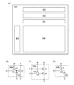
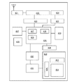
図1(A)に、プログラマブルLSIの構成を模式的に示す。プログラマブルLSIは、ロジックエレメント310を複数と、メモリエレメント300と、を有する。図1(A)では、ロジックエレメント310を3つ代表的に示した。ロジックエレメントの数は、任意の個数とすることができる。また、プログラマブルLSIは、ロジックエレメント310を複数と、メモリエレメント300と、の組を更に複数有していてもよい。また、プログラマブルLSIは、更に、マルチプライヤ(乗算器)や、RAMブロックや、PLLブロックや、I/Oエレメントを有していてもよい。マルチプライヤ(乗算器)は、複数のデータの乗算を高速で行う機能を有する。RAMブロックは、メモリとして任意のデータを記憶する機能を有する。PLLブロックは、クロック信号をプログラマブルLSI内部の回路に供給する機能を有する。I/Oエレメントは、プログラマブルLSIと外部回路との信号の受け渡しを制御する機能を有する。
FIG. 1A schematically shows the configuration of a programmable LSI. The programmable LSI has a plurality of
ロジックエレメント310は、コンフィギュレーションメモリ311と、ルックアップテーブル312と、選択回路314と、レジスタ313とを有する。なお、更に、別のレジスタを有していてもよいし、マルチプレクサを有していてもよいし、スイッチを有していてもよい。
The
ロジックエレメント310において、ルックアップテーブル312は、コンフィギュレーションメモリ311に記憶されたコンフィギュレーションデータに応じて、異なる演算処理を行う。
In the
ロジックエレメント310において、選択回路314は、コンフィギュレーションメモリ311に記憶されたコンフィギュレーションデータに応じて、他のロジックエレメント310との電気的接続を変更する。例えば、選択回路314は、プログラマブルLSIに設けられた配線リソースにおける電気的接続関係を変更する。こうして、ロジックエレメント310同士の電気的接続関係や、ロジックエレメント310とその他回路(マルチプライヤ(乗算器)や、RAMブロックや、PLLブロックや、I/Oエレメント等)との電気的接続関係を変更する。
In the
ロジックエレメント310において、レジスタ313は、ルックアップテーブル312の出力信号とクロック信号(CLK)とが入力され、当該出力信号に対応する信号をクロック信号(CLK)に同期して出力する。レジスタ313の出力信号や、ルックアップテーブル312の出力信号を、ロジックエレメント310の出力信号として、選択回路314によって選択された電気的接続に応じて別のロジックエレメント310(例えば、隣接するロジックエレメント310)等へ出力する。ここで、ロジックエレメント310において、レジスタ313の出力信号、またはルックアップテーブル312の出力信号を選択するマルチプレクサ等を設けてもよい。
In the
なお、図1(A)では、1つのロジックエレメント310内において、コンフィギュレーションメモリ311が1カ所にまとまって配置される構成を模式的に示したがこれに限定されない。コンフィギュレーションメモリ311は、複数に分散され、ルックアップテーブル312や選択回路314等にそれぞれ設けられていてもよい。
1A schematically illustrates a configuration in which the
なお、図1(A)に示したロジックエレメント310の構成において、レジスタ313を省略することもできる。また、レジスタ313を有するロジックエレメント310と、レジスタ313を省略したロジックエレメント310の両方が混在するプログラマブルLSIであってもよい。レジスタ313を省略したロジックエレメント310では、ルックアップテーブル312の出力を、ロジックエレメント310の出力とすることができる。
Note that the
(コンフィギュレーションメモリ311の構成)
コンフィギュレーションメモリ311に用いる記憶回路の一態様を図1(C)に示す。図1(C)において、コンフィギュレーションメモリ311に用いる記憶回路は、揮発性の記憶回路200と、不揮発性の記憶回路10と、の組でなる。コンフィギュレーションメモリ311は、当該記憶回路を複数有する構成とすることができる。
(Configuration Memory of Configuration Memory 311)
One mode of a memory circuit used for the
図1(C)における不揮発性の記憶回路10の構成を図1(B)に示す。図1(B)において、不揮発性の記憶回路10は、トランジスタ11と容量素子12とを有する。なお、図1(B)では、トランジスタ11のチャネルが酸化物半導体層に形成されていることを示すため、「OS」の符号を付している。トランジスタ11のゲートは端子Wと電気的に接続され、トランジスタ11のソース及びドレインの一方は端子Bと電気的に接続される。トランジスタ11のソース及びドレインの他方は、容量素子12の一対の電極のうちの一方と電気的に接続される。容量素子12の一対の電極のうちの他方は、端子Cと電気的に接続される。
A structure of the
不揮発性の記憶回路10では、容量素子12の一対の電極のうちの一方の電位(またはそれに対応する電荷量)をデータに応じて制御することによって、データを記憶する。例えば、容量素子12に所定の電荷が充電された状態を「1」に対応させ、容量素子12に電荷が充電されていない状態を「0」に対応させることによって、1ビットのデータを記憶することができる。不揮発性の記憶回路10では、トランジスタ11のオフ電流が極めて小さいため、トランジスタ11をオフ状態とすることにより、電源電圧の供給が停止した後も容量素子12の一対の電極のうちの一方の電位、即ちデータを長期間に渡って保持することが可能となる。また、不揮発性の記憶回路10では、データに対応する信号電位を所定のノード(容量素子12の一対の電極のうちの一方)に入力し、トランジスタ11をオフ状態として、当該ノードをフローティング状態とすることにより、データを記憶する構成である。そのため、不揮発性の記憶回路10において、データの書き換えを繰り返すことによる疲労は少なく、データの書き換え可能な回数を多くすることができる。
The
図1(C)における揮発性の記憶回路200は、演算回路201及び演算回路202を有し、演算回路201の出力が演算回路202に入力され、演算回路202の出力が演算回路201に入力されるような、帰還ループを有する。揮発性の記憶回路200としては、フリップフロップ回路やラッチ回路がある。なお、演算回路201及び演算回路202の一方または両方において、クロック信号が入力される構成であってもよい。
A
図1(C)において、不揮発性の記憶回路10の端子Bは、演算回路202の入力端子と演算回路201の出力端子との間に存在するノードMと電気的に接続される。また揮発性の記憶回路200は、ノードMと演算回路201の出力端子との電気的接続を選択するスイッチ203を有し、スイッチ203は制御信号SEL0によって導通状態または非導通状態が選択される。なお、演算回路201が制御信号(例えば、クロック信号等)に応じて選択的に信号を出力する回路の場合には、スイッチ203を必ずしも設ける必要はなく、省略することも可能である。不揮発性の記憶回路10の端子Wには制御信号SELが入力されている。なお、不揮発性の記憶回路10の端子Cには、一定の電位、例えば、低電源電位が入力される構成とすることができる。
In FIG. 1C, the terminal B of the
図1(C)に示す揮発性の記憶回路200と不揮発性の記憶回路10との組でなる記憶回路を有するコンフィギュレーションメモリ311を採用したプログラマブルLSIにおいて、ノーマリオフの駆動方法を適用する場合について説明する。
Description will be made regarding a case where a normally-off driving method is applied to a programmable LSI that employs a
(電源電圧供給時の動作)
当該組に電源電圧が供給されている間、つまり当該組を有するコンフィギュレーションメモリ311に電源電圧が供給されている間は、制御信号SEL0によってスイッチ203は導通状態である。こうして、揮発性の記憶回路200は、演算回路201及び演算回路202でなる帰還ループによってデータを保持する。つまり、図1(C)に示す組において、入力されるデータ(コンフィギュレーションデータ)は揮発性の記憶回路200の帰還ループによって保持され、また揮発性の記憶回路200の帰還ループからデータ(コンフィギュレーションデータ)が出力される。このような揮発性の記憶回路200の帰還ループによるデータ(コンフィギュレーションデータ)の保持及び出力は、高速に行うことが可能である。こうして、動的コンフィギュレーションを容易に行うこともできる。
(Operation when supplying power supply voltage)
While the power supply voltage is supplied to the set, that is, while the power supply voltage is supplied to the
(データ格納の動作)
上記のとおり、揮発性の記憶回路200の帰還ループによるデータ(コンフィギュレーションデータ)の保持が行われると同時に、または当該データ(コンフィギュレーションデータ)の保持が行われた後に、制御信号SEL0によってスイッチ203を導通状態としたまま、制御信号SELによって、不揮発性の記憶回路10のトランジスタ11をオン状態とする。こうして、揮発性の記憶回路200のノードMの電位を、不揮発性の記憶回路10の容量素子12の一対の電極のうちの一方に入力して、揮発性の記憶回路200に保持されたデータを不揮発性の記憶回路10に記憶させることができる。こうして、データの格納を行うことができる。
(Data storage operation)
As described above, the data (configuration data) is held by the feedback loop of the
(データ待機の動作)
データ格納の後、不揮発性の記憶回路10のトランジスタ11をオフ状態とすることによって、不揮発性の記憶回路10に記憶されたデータが揮発性の記憶回路200からの信号によって変動しないような状態とする。こうしてデータの待機を行うことができる。不揮発性の記憶回路10では、トランジスタ11のオフ電流が極めて小さいため、トランジスタ11をオフ状態とすることにより、電源電圧の供給が停止した後も容量素子12の一対の電極のうちの一方の電位、即ちデータを長期間に渡って保持することが可能となる。
(Data waiting operation)
After data storage, the
以上のとおり、データの待機を行った後、コンフィギュレーションメモリ311への電源電圧の供給を停止する。
As described above, after waiting for data, the supply of power supply voltage to the
(データ供給の動作)
当該組に電源電圧供給が選択された後、つまり当該組を有するコンフィギュレーションメモリ311に電源電圧が供給されはじめた後に、制御信号SEL0によってスイッチ203を非導通状態とし、且つ制御信号SELによって、不揮発性の記憶回路10のトランジスタ11をオン状態とする。こうして、揮発性の記憶回路200のノードMに、不揮発性の記憶回路10の容量素子12の一対の電極のうちの一方の電位(またはそれに対応する電荷量)を入力する。その後、制御信号SEL0によってスイッチ203を導通状態とする。こうして、不揮発性の記憶回路10に保持されていたデータ(コンフィギュレーションデータ)を、揮発性の記憶回路200に入力し、帰還ループによって保持させることができる。このように揮発性の記憶回路200にデータを供給することができる。ここで、揮発性の記憶回路200は、不揮発性の記憶回路10よりもデータ書き込み及び読み出しのスピードが速い。よって、電源電圧供給が選択された組における動作速度を速くすることが可能である。こうして、動的コンフィギュレーションを容易に行うこともできる。
(Data supply operation)
After power supply voltage supply is selected for the set, that is, after power supply voltage starts to be supplied to the
なお、演算回路201を制御信号(例えば、クロック信号等)に応じて選択的に信号を出力する回路として、スイッチ203を省略する構成を採用した場合には、上記説明においてスイッチ203が非導通状態となる際に、演算回路201の出力が無い(不定となる)ように演算回路201を制御する。演算回路201以外の駆動方法は上記と同様とすることができる。
Note that when the
以上が、図1(C)に示す揮発性の記憶回路200と不揮発性の記憶回路10との組でなる記憶回路を有するコンフィギュレーションメモリ311を採用したプログラマブルLSIにおけるノーマリオフの駆動方法についての説明である。
The above is the description of the normally-off driving method in the programmable LSI that employs the
(コンフィギュレーションメモリ311のバリエーション1)
コンフィギュレーションメモリ311に用いる記憶回路は、図1(C)に示した構成に限定されない。例えば、図1(D)に示す構成とすることができる。
(
The memory circuit used for the
例えば、1ビットのデータを記憶する揮発性の記憶回路1つに対して、1ビットのデータを記憶する不揮発性の記憶回路が複数対応するように設けられていてもよい。図1(D)に示す構成では、揮発性の記憶回路200に対して、不揮発性の記憶回路10−1及び不揮発性の記憶回路10−2が設けられている。図1(D)に示す構成において、不揮発性の記憶回路10−1及び不揮発性の記憶回路10−2はそれぞれ、図1(B)における不揮発性の記憶回路10と同様の構成とすることができるので、詳細な説明は省略する。なお、不揮発性の記憶回路10−1の端子Wには制御信号SEL1が入力され、不揮発性の記憶回路10−2の端子Wには制御信号SEL2が入力され、不揮発性の記憶回路10−1の端子B及び不揮発性の記憶回路10−2の端子Bは供にノードMと電気的に接続されている。また、揮発性の記憶回路200は、図1(B)における揮発性の記憶回路200と同様の構成とすることができるので、詳細な説明は省略する。
For example, a single volatile storage circuit that stores 1-bit data may be provided so as to correspond to a plurality of nonvolatile storage circuits that store 1-bit data. In the structure illustrated in FIG. 1D, a nonvolatile memory circuit 10-1 and a nonvolatile memory circuit 10-2 are provided for the
図1(D)に示した構成の記憶回路を有するコンフィギュレーションメモリ311では、ノーマリオフの駆動方法を行う場合において、電源電圧供給停止前に、制御信号SEL1及び制御信号SEL2によって、複数の不揮発性の記憶回路(不揮発性の記憶回路10−1及び不揮発性の記憶回路10−2)それぞれに異なるデータ(コンフィギュレーションデータ)を格納することができる。電源電圧供給停止時において、これらのデータを待機することができる。そして、電源電圧の供給を選択された際に、制御信号SEL1及び制御信号SEL2によって、複数の不揮発性の記憶回路(不揮発性の記憶回路10−1及び不揮発性の記憶回路10−2)から1つの不揮発性の記憶回路を選択し、選択された不揮発性の記憶回路に保持された1ビットのデータを揮発性の記憶回路200に提供することができる。こうして、電源電圧供給後のコンフィギュレーションメモリ311の状態を複数の状態から選択することが可能となる。また、複数の不揮発性の記憶回路(不揮発性の記憶回路10−1及び不揮発性の記憶回路10−2)から1つの不揮発性の記憶回路を選択し、選択された不揮発性の記憶回路に保持されたデータを揮発性の記憶回路200に提供することによって、動的コンフィギュレーションを容易に行うこともできる。
In the
(コンフィギュレーションメモリ311のバリエーション2)
また例えば、コンフィギュレーションメモリ311に用いる記憶回路は、図2(C)に示す構成とすることもできる。図2(C)における揮発性の記憶回路200では、図1(C)におけるスイッチ203は必ずしも必要ないため、設けられていない。図2(C)における不揮発性の記憶回路10の端子Fは、図2(A)に示すように、容量素子12の一対の電極のうちの一方と電気的に接続されている。図2(C)では、不揮発性の記憶回路10の端子Fは演算回路204及びスイッチ205を介して、揮発性の記憶回路の演算回路202の出力端子及び演算回路201の入力端子と電気的に接続されている。演算回路204として、例えばインバータ224を用いることができる。また、スイッチ205は制御信号SELRによって、導通状態または非導通状態が選択される。
(
For example, the memory circuit used for the
図2(C)に示す揮発性の記憶回路200と不揮発性の記憶回路10との組でなる記憶回路を有するコンフィギュレーションメモリ311を採用したプログラマブルLSIにおいて、ノーマリオフの駆動方法を適用する場合について説明する。
A description will be given of a case where a normally-off driving method is applied to a programmable LSI that employs a
(電源電圧供給時の動作)
当該組に電源電圧が供給されている間、つまり当該組を有するコンフィギュレーションメモリ311に電源電圧が供給されている間は、制御信号SELRによってスイッチ205は非導通状態である。こうして、揮発性の記憶回路200は、演算回路201及び演算回路202でなる帰還ループによってデータを保持する。つまり、図2(C)に示す組において、入力されるデータ(コンフィギュレーションデータ)は揮発性の記憶回路200の帰還ループによって保持され、また揮発性の記憶回路200の帰還ループからデータ(コンフィギュレーションデータ)が出力される。このような揮発性の記憶回路200の帰還ループによるデータ(コンフィギュレーションデータ)の保持及び出力は、高速に行うことが可能である。こうして、動的コンフィギュレーションを容易に行うこともできる。
(Operation when supplying power supply voltage)
While the power supply voltage is supplied to the set, that is, while the power supply voltage is supplied to the
(データ格納の動作)
上記のとおり、揮発性の記憶回路200の帰還ループによるデータ(コンフィギュレーションデータ)の保持が行われると同時に、または当該データ(コンフィギュレーションデータ)の保持が行われた後に、制御信号SELRによってスイッチ205は非導通状態としたまま、制御信号SELによって、不揮発性の記憶回路10のトランジスタ11をオン状態とする。こうして、揮発性の記憶回路200のノードMの電位を、不揮発性の記憶回路10の容量素子12の一対の電極のうちの一方に入力して、揮発性の記憶回路200に保持されたデータを不揮発性の記憶回路10に記憶させることができる。こうして、データの格納を行うことができる。
(Data storage operation)
As described above, the data (configuration data) is held by the feedback loop of the
(データ待機の動作)
データ格納の後、不揮発性の記憶回路10のトランジスタ11をオフ状態とすることによって、不揮発性の記憶回路10に記憶されたデータが揮発性の記憶回路200からの信号によって変動しないような状態とする。こうして、データの待機を行うことができる。不揮発性の記憶回路10では、トランジスタ11のオフ電流が極めて小さいため、トランジスタ11をオフ状態とすることにより、電源電圧の供給が停止した後も容量素子12の一対の電極のうちの一方の電位、即ちデータを長期間に渡って保持することが可能となる。
(Data waiting operation)
After data storage, the
以上のとおり、データの待機を行った後、コンフィギュレーションメモリ311への電源電圧の供給を停止する。
As described above, after waiting for data, the supply of power supply voltage to the
(データ供給の動作)
当該組に電源電圧供給が選択された後、つまり当該組を有するコンフィギュレーションメモリ311に電源電圧が供給されはじめた後に、制御信号SELRによって、スイッチ205を導通状態とする。こうして、揮発性の記憶回路200のノードMbに、不揮発性の記憶回路10の容量素子12の一対の電極のうちの一方の電位(またはそれに対応する電荷量)に対応する信号をインバータ224によって反転させて入力することができる。こうして、不揮発性の記憶回路10に保持されていたデータ(コンフィギュレーションデータ)を、揮発性の記憶回路200に入力し、帰還ループによって保持させることができる。このように揮発性の記憶回路200にデータを供給することができる。ここで、揮発性の記憶回路200は、不揮発性の記憶回路10よりもデータ書き込み及び読み出しのスピードが速い。よって、電源電圧供給が選択された組における動作速度を速くすることが可能である。こうして、動的コンフィギュレーションを容易に行うこともできる。
(Data supply operation)
After the power supply voltage supply is selected for the set, that is, after the power supply voltage starts to be supplied to the
なお、演算回路204を制御信号(例えば、クロック信号等)に応じて選択的に信号を出力する回路として、スイッチ205を省略する構成を採用することもできる。この場合には、上記説明においてスイッチ205が非導通状態となる際に、演算回路204の出力が無い(不定となる)ように演算回路204を制御する。演算回路204以外の駆動方法は上記と同様とすることができる。
Note that a configuration in which the switch 205 is omitted may be employed as the circuit that selectively outputs the
以上が、図2(C)に示す揮発性の記憶回路200と不揮発性の記憶回路10との組でなる記憶回路を有するコンフィギュレーションメモリ311を採用したプログラマブルLSIにおけるノーマリオフの駆動方法についての説明である。
The above is the description of the normally-off driving method in the programmable LSI that employs the
(コンフィギュレーションメモリ311のバリエーション3)
また例えば、コンフィギュレーションメモリ311に用いる記憶回路は、図2(B)に示す構成とすることもできる。図2(B)に示した記憶回路では、揮発性の記憶回路200内に不揮発性の記憶回路10が含まれる。図2(B)における不揮発性の記憶回路10の端子Fは、図2(A)に示すように、容量素子12の一対の電極のうちの一方と電気的に接続されている。
(Variation 3 of the configuration memory 311)
For example, the memory circuit used for the
図2(B)に示す揮発性の記憶回路200と不揮発性の記憶回路10との組でなる記憶回路を有するコンフィギュレーションメモリ311を採用したプログラマブルLSIにおいて、ノーマリオフの駆動方法を適用する場合について説明する。
A description will be given of a case where a normally-off driving method is applied to a programmable LSI that employs a
(電源電圧供給時の動作)
当該組に電源電圧が供給されている間、つまり当該組を有するコンフィギュレーションメモリ311に電源電圧が供給されている間は、制御信号SELによって不揮発性の記憶回路10のトランジスタ11はオン状態である。こうして、揮発性の記憶回路200は、演算回路201及び演算回路202でなる帰還ループによってデータを保持する。つまり、図2(B)に示す組において、入力されるデータは揮発性の記憶回路200の帰還ループによって保持され、また揮発性の記憶回路200の帰還ループからデータが出力される。このような揮発性の記憶回路200の帰還ループによるデータの保持及び出力は、高速に行うことが可能である。こうして、動的コンフィギュレーションを容易に行うこともできる。
(Operation when supplying power supply voltage)
While the power supply voltage is supplied to the set, that is, while the power supply voltage is supplied to the
(データ格納の動作)
上記のとおり、揮発性の記憶回路200の帰還ループによるデータの保持が行われると同時に、揮発性の記憶回路200のノードMの電位は、不揮発性の記憶回路10の容量素子12の一対の電極のうちの一方に入力され、揮発性の記憶回路200に保持されたデータを不揮発性の記憶回路10に記憶させることができる。こうして、データの格納を行うことができる。
(Data storage operation)
As described above, data is held by the feedback loop of the
(データ待機の動作)
データ格納の後、制御信号SELによって不揮発性の記憶回路10のトランジスタ11をオフ状態とすることによって、不揮発性の記憶回路10に記憶されたデータが揮発性の記憶回路200の演算回路201からの信号によって変動しないような状態とする。こうして、データの待機を行うことができる。
(Data waiting operation)
After the data is stored, the
以上のとおり、データの待機を行った後、電源電圧の供給を停止する。 As described above, after waiting for data, the supply of the power supply voltage is stopped.
(データ供給の動作)
当該組に電源電圧供給が選択された後、つまり当該組を有するコンフィギュレーションメモリ311に電源電圧が再び供給されはじめた後に、制御信号SELによって不揮発性の記憶回路10のトランジスタ11をオン状態とする。こうして、揮発性の記憶回路200のノードMに、不揮発性の記憶回路10の容量素子12の一対の電極のうちの一方の電位(または対応する電荷)を入力する。こうして、不揮発性の記憶回路10に保持されていたデータを、揮発性の記憶回路200の帰還ループによって保持させることができる。このように揮発性の記憶回路200にデータを供給することができる。ここで、揮発性の記憶回路200は、不揮発性の記憶回路10よりもデータ書き込み及び読み出しのスピードが速い。よって、電源電圧供給が選択された組における動作速度を速くすることが可能である。こうして、動的コンフィギュレーションを容易に行うこともできる。
(Data supply operation)
After the power supply voltage supply is selected for the set, that is, after the power supply voltage starts to be supplied again to the
なお、上記データ供給を行う際、電源電圧供給が選択された後、制御信号SELによって不揮発性の記憶回路10のトランジスタ11をオン状態とするとき、演算回路201から信号が出力されない(演算回路201の出力が不定である)構成とすることが好ましい。例えば、演算回路201として、制御信号(例えば、クロック信号等)に応じて選択的に信号を出力する回路を用いることが好ましい。また例えば、演算回路201の出力端子と、不揮発性の記憶回路100の端子Bとの間にスイッチ等を設ける構成として、電源電圧供給が選択された後、制御信号SELによって不揮発性の記憶回路10のトランジスタ11をオン状態とする際に、当該スイッチを非導通状態とすることが好ましい。
Note that when supplying the data, after the power supply voltage supply is selected, when the
以上が、図2(B)に示す揮発性の記憶回路200と不揮発性の記憶回路10との組でなる記憶回路を有するコンフィギュレーションメモリ311を採用したプログラマブルLSIにおけるノーマリオフの駆動方法についての説明である。
The above is the description of the normally-off driving method in the programmable LSI that employs the
本実施の形態に示すプログラマブルLSIでは、電源電圧供給停止後、再び電源電圧が供給された際に、コンフィギュレーションメモリへのコンフィギュレーションデータの書き込みが不要となり、プログラマブルLSIの起動時間を短くすることができる。そのため、プログラマブルLSIにおいて、電源電圧供給を頻繁に停止することが可能となり、ノーマリオフの駆動方法を適用して消費電力を大幅に低減することができる。 In the programmable LSI shown in this embodiment, when the power supply voltage is supplied again after the supply of the power supply voltage is stopped, it is not necessary to write the configuration data to the configuration memory, and the startup time of the programmable LSI can be shortened. it can. Therefore, in the programmable LSI, the power supply voltage supply can be frequently stopped, and the power consumption can be significantly reduced by applying the normally-off driving method.
また、電源電圧が供給されている間は、揮発性の記憶回路200を用いてコンフィギュレーションデータの記憶及び出力を行うことができる。ここで、フリップフロップ回路やラッチ回路等の揮発性の記憶回路は動作速度が速い。そのため、コンフィギュレーションメモリ311のアクセススピードを高速化することが可能である。こうして、動的コンフィギュレーションにも対応可能なプログラマブルLSIを提供することができる。更に、コンフィギュレーションメモリ311に用いる不揮発性の記憶回路として、書き込み可能な回数が多く信頼性の高い回路を用いるため、プログラマブルLSIの耐久性、信頼性を向上させることができる。
In addition, while the power supply voltage is supplied, the configuration data can be stored and output using the
本実施の形態は、他の実施の形態と適宜組み合わせて実施することが可能である。 This embodiment can be implemented in appropriate combination with any of the other embodiments.
(実施の形態2)
本実施の形態では、メモリエレメント300の具体的な一態様について説明する。メモリエレメント300は、複数の記憶回路を有する構成とすることができる。メモリエレメント300に用いる記憶回路としては、チャネルが酸化物半導体層に形成されるトランジスタと、当該トランジスタがオフ状態となることによってフローティングとなるノードと、を有する記憶回路(以下、メモリセルと呼ぶ)を用いることができる。メモリセルの一態様を、図5(B)乃至図5(D)に示す。
(Embodiment 2)
In this embodiment, a specific mode of the
(メモリセルの構成1)
図5(B)に示すメモリセル100aは、トランジスタ101と、トランジスタ102と、容量素子103とを有する。トランジスタ101はチャネルが酸化物半導体層に形成される。なお、図5(B)では、トランジスタ101のチャネルが酸化物半導体層に形成されていることを示すため、「OS」の符号を付している。トランジスタ101のゲートは端子Wと電気的に接続され、トランジスタ101のソース及びドレインの一方は端子Dと電気的に接続される。トランジスタ101のソース及びドレインの他方は、トランジスタ102のゲートと電気的に接続される。トランジスタ102のソース及びドレインの一方は、端子Sと電気的に接続される。トランジスタ102のソース及びドレインの他方は、端子Bと電気的に接続される。容量素子103の一対の電極のうちの一方は、トランジスタ102のゲートと電気的に接続される。容量素子103の一対の電極のうちの他方は、端子Cと電気的に接続される。ここで、各端子は、配線や電極と電気的に接続される構成とすることができる。
(
A
端子Wに電気的に接続される配線を書き込みワード線、端子Cに電気的に接続される配線を読み出しワード線、端子Dに電気的に接続される配線をデータ線、端子Bに電気的に接続される配線をビット線とも呼ぶ。なお、データ線とビット線は共有することもできる。ここで、データ線とビット線とを共有して同じ配線とした場合に、当該配線はビット線と呼ぶことにする。 The wiring electrically connected to the terminal W is a write word line, the wiring electrically connected to the terminal C is a read word line, and the wiring electrically connected to the terminal D is electrically connected to the data line and the terminal B. The wiring to be connected is also called a bit line. The data line and the bit line can be shared. Here, when the data line and the bit line are shared to form the same wiring, the wiring is referred to as a bit line.
ここで、チャネルが酸化物半導体層に形成されるトランジスタ101がオフ状態となることによってフローティングとなるノードは、トランジスタ102のゲート、または容量素子103の一対の電極のうちの一方とすることができる。
Here, the node which is floated when the
(メモリセル100aの駆動方法)
図5(B)に示したメモリセル100aの駆動方法について説明する。
(Driving method of
A driving method of the
まず、メモリセル100aにデータを書き込む動作について説明する。ゲートに入力される制御信号(端子Wに入力される制御信号)によってオン状態を選択されたトランジスタ101を介して、データ(コンフィギュレーションデータ)に対応する信号電位(端子Dに入力される信号電位)をトランジスタ102のゲート、及び容量素子103の一対の電極のうちの一方に入力する。その後、ゲートに入力される制御信号(端子Wに入力される制御信号)によってトランジスタ101をオフ状態とすることによって、トランジスタ102のゲート、及び容量素子103の一対の電極のうちの一方に当該信号電位を保持する。こうして、メモリセル100aにデータを書き込むことができる。
First, an operation for writing data in the
ここで、酸化物半導体層にチャネルが形成されるトランジスタ101はオフ電流が著しく小さい。そのため、メモリセル100aに電源電圧が供給されない間も、トランジスタ102のゲート、及び容量素子103の一対の電極のうちの一方の電位(信号電位)は長期間にわたって保持される。よって、電源電圧の供給を停止した後もメモリセル100aはデータを保持することができる。
Here, the
次いで、メモリセル100aからデータを読み出す動作について説明する。トランジスタ102のソース(端子S)、及び容量素子103の一対の電極のうちの他方(端子C)の電位を、当該信号電位に応じてトランジスタ102のソースとドレイン間の状態が異なるような電位とする。ここで、トランジスタ102のソースとドレイン間の状態とは、非導通状態であるか導通状態であるかを示すものとする。トランジスタ102のソースとドレイン間の状態を検出することによって、メモリセル100aに保持されたデータを読み出す。
Next, an operation of reading data from the
なお、端子Cの電位を制御することによって、メモリセル100aに保持されたデータに関わらず、トランジスタ102をオン状態、つまり、トランジスタ102のソースとドレイン間を導通状態とすることもできる。また、端子Cの電位を制御することによって、メモリセル100aに保持されたデータに関わらず、トランジスタ102をオフ状態、つまり、トランジスタ102のソースとドレイン間を非導通状態とすることもできる。
Note that by controlling the potential of the terminal C, the
以上が、メモリセル100aの駆動方法についての説明である。
The above is the description of the driving method of the
メモリエレメント300が有する複数のメモリセル100aそれぞれにおいて、上記のようにデータの書き込み及び読み出しを行うことによって、メモリエレメント300は複数のデータ(コンフィギュレーションデータ)の書き込み及び読み出しを行うことができる。
By writing and reading data as described above in each of the plurality of
(メモリセルの構成2)
上記(メモリセルの構成1)とは異なる構成のメモリセルについて説明する。
(Memory cell configuration 2)
A memory cell having a configuration different from the above (Memory cell configuration 1) will be described.
図5(C)に示すメモリセル100bは、トランジスタ101と、トランジスタ102と、トランジスタ141とを有する。トランジスタ101はチャネルが酸化物半導体層に形成される。なお、図5(C)では、トランジスタ101のチャネルが酸化物半導体層に形成されていることを示すため、「OS」の符号を付している。トランジスタ101のゲートは端子Wと電気的に接続される。トランジスタ101のソース及びドレインの一方は端子Dと電気的に接続される。トランジスタ101のソース及びドレインの他方は、トランジスタ102のゲートと電気的に接続される。トランジスタ102のソース及びドレインの一方は、端子Sと電気的に接続される。トランジスタ102のソース及びドレインの他方は、トランジスタ141のソースとドレイン間を介して端子Bと電気的に接続され、トランジスタ141のゲートは端子Xと電気的に接続される。ここで、各端子は、配線や電極と電気的に接続される構成とすることができる。
A
端子Wに電気的に接続される配線を書き込みワード線、端子Xに電気的に接続される配線を読み出しワード線、端子Dに電気的に接続される配線をデータ線、端子Bに電気的に接続される配線をビット線とも呼ぶ。なお、データ線とビット線は共有することもできる。ここで、データ線とビット線とを共有して同じ配線とした場合に、当該配線はビット線と呼ぶことにする。 The wiring electrically connected to the terminal W is a write word line, the wiring electrically connected to the terminal X is a read word line, the wiring electrically connected to the terminal D is electrically connected to the data line, and the terminal B The wiring to be connected is also called a bit line. The data line and the bit line can be shared. Here, when the data line and the bit line are shared to form the same wiring, the wiring is referred to as a bit line.
ここで、チャネルが酸化物半導体層に形成されるトランジスタ101がオフ状態となることによってフローティングとなるノードは、トランジスタ102のゲートとすることができる。
Here, a node which is floated when the
(メモリセル100bの駆動方法)
図5(C)に示したメモリセル100bの駆動方法について説明する。
(Driving method of
A driving method of the
まず、メモリセル100bにデータを書き込む動作について説明する。ゲートに入力される制御信号(端子Wに入力される制御信号)によってオン状態を選択されたトランジスタ101を介して、データ(コンフィギュレーションデータ)に対応する信号電位(端子Dに入力される信号電位)をトランジスタ102のゲートに入力する。その後、ゲートに入力される制御信号(端子Wに入力される制御信号)によってトランジスタ101をオフ状態とすることによって、トランジスタ102のゲートに当該信号電位を保持する。こうして、メモリセル100bにデータを書き込むことができる。
First, an operation for writing data in the
ここで、酸化物半導体層にチャネルが形成されるトランジスタ101はオフ電流が著しく小さい。そのため、メモリセル100bに電源電圧が供給されない間も、トランジスタ102のゲートの電位(信号電位)は長期間にわたって保持される。よって、電源電圧の供給を停止した後もメモリセル100bはデータを保持することができる。
Here, the
次いで、メモリセル100bからデータを読み出す動作について説明する。トランジスタ102のソース(端子S)を、当該信号電位に応じてトランジスタ102のソースとドレイン間の状態が異なるような電位とする。ここで、トランジスタ102のソースとドレイン間の状態とは、非導通状態であるか導通状態であるかを示すものとする。そして、ゲートに入力される制御信号(端子Xに入力される制御信号)によってトランジスタ141をオン状態として、トランジスタ102のソースとドレイン間の状態を検出することによって、メモリセル100bに保持されたデータを読み出す。
Next, an operation of reading data from the
なお、端子S(端子Sに電気的に接続される配線)は、一定の電位(例えば、接地電位等の低電源電位)が入力される構成とすることができる。 Note that the terminal S (a wiring electrically connected to the terminal S) can have a structure in which a constant potential (for example, a low power supply potential such as a ground potential) is input.
以上が、メモリセル100bの駆動方法についての説明である。
The above is the description of the driving method of the
メモリエレメント300が有する複数のメモリセル100bそれぞれにおいて、上記のようにデータの書き込み及び読み出しを行うことによって、メモリエレメント300は複数のデータ(コンフィギュレーションデータ)の書き込み及び読み出しを行うことができる。
By writing and reading data in each of the plurality of
(メモリセルの構成3)
上記(メモリセルの構成1)や(メモリセルの構成2)とは異なる構成のメモリセルについて説明する。
(Configuration 3 of memory cell)
A memory cell having a configuration different from the above (Memory cell configuration 1) and (Memory cell configuration 2) will be described.
図5(D)に示すメモリセル100cは、トランジスタ104と、容量素子105とを有する。トランジスタ104はチャネルが酸化物半導体層に形成される。図5(D)では、トランジスタ104のチャネルが酸化物半導体層に形成されていることを示すため、「OS」の符号を付している。トランジスタ104のゲートは端子Wと電気的に接続される。トランジスタ104のソース及びドレインの一方は端子Bと電気的に接続される。トランジスタ104のソース及びドレインの他方は、容量素子105の一対の電極のうちの一方と電気的に接続される。ここで、各端子は、配線や電極と電気的に接続される構成とすることができる。
A
端子Wに電気的に接続される配線をワード線、端子Bに電気的に接続される配線をビット線とも呼ぶ。 A wiring electrically connected to the terminal W is also called a word line, and a wiring electrically connected to the terminal B is also called a bit line.
ここで、チャネルが酸化物半導体層に形成されるトランジスタ104がオフ状態となることによってフローティングとなるノードは、容量素子105の一対の電極のうちの一方とすることができる。
Here, a node which is floated when the
(メモリセル100cの駆動方法)
図5(D)に示したメモリセル100cの駆動方法について説明する。
(Driving method of
A driving method of the
まず、メモリセル100cにデータを書き込む動作について説明する。ゲートに入力される制御信号(端子Wに入力される制御信号)によってオン状態を選択されたトランジスタ104を介して、データ(コンフィギュレーションデータ)に対応する信号電位(端子Bに入力される信号電位)を容量素子105の一対の電極のうちの一方に入力する。その後、ゲートに入力される制御信号(端子Wに入力される制御信号)によってトランジスタ104をオフ状態とすることによって、容量素子105に当該信号電位を保持する。こうして、メモリセル100cにデータを書き込むことができる。
First, an operation for writing data in the
ここで、酸化物半導体層にチャネルが形成されるトランジスタ104はオフ電流が著しく小さい。そのため、メモリセル100cに電源電圧が供給されない間も、容量素子105の一対の電極のうちの一方の電位(信号電位)は長期間にわたって保持される。よって、電源電圧の供給を停止した後もメモリセル100cはデータを保持することができる。
Here, the
次いで、メモリセル100cからデータを読み出す動作について説明する。ゲートに入力される制御信号(端子Wに入力される制御信号)によってトランジスタ104をオン状態として、端子Bから容量素子105の一対の電極のうちの一方に保持されていた信号電位(当該信号電位に対応する電荷量ということもできる)を検出することによって、メモリセル100cに保持されたデータを読み出す。
Next, an operation of reading data from the
なお、容量素子105の一対の電極のうちの他方は、端子Cと電気的に接続される構成とすることができる。端子Cは、一定の電位(例えば、接地電位等の低電源電位)が入力される構成とすることができる。 Note that the other of the pair of electrodes of the capacitor 105 can be electrically connected to the terminal C. The terminal C can be configured to receive a constant potential (for example, a low power supply potential such as a ground potential).
以上が、メモリセル100cの駆動方法についての説明である。
The above is the description of the driving method of the
メモリエレメント300が有する複数のメモリセル100cそれぞれにおいて、上記のようにデータの書き込み及び読み出しを行うことによって、メモリエレメント300は複数のデータ(コンフィギュレーションデータ)の書き込み及び読み出しを行うことができる。
By writing and reading data in each of the plurality of
(メモリセルのバリエーション)
上述した(メモリセルの構成1)、(メモリセルの構成2)、(メモリセルの構成3)において、メモリセルは更に、ダイオードや、抵抗素子や、スイッチを有していても良い。スイッチとしては、例えばアナログスイッチや、トランジスタ等を用いることができる。例えば、(メモリセルの構成2)において、更に容量素子を有し、当該容量素子の一対の電極のうちの一方はトランジスタ102のゲートと電気的に接続されていてもよい。当該容量素子の一対の電極のうちの他方は、一定の電位(例えば、接地電位等の低電源電位)が入力される構成とすることができる。
(Variation of memory cells)
In the above-described (Memory Cell Configuration 1), (Memory Cell Configuration 2), and (Memory Cell Configuration 3), the memory cell may further include a diode, a resistance element, and a switch. As the switch, for example, an analog switch, a transistor, or the like can be used. For example, in (Memory Cell Structure 2), a capacitor may be further provided, and one of the pair of electrodes of the capacitor may be electrically connected to the gate of the
なお、メモリエレメント300は、ロジックエレメント310の状態(ルックアップテーブル312によって行われる論理演算の種類、及び選択回路314が選択する接続関係)に対応するコンフィギュレーションデータを複数組記憶するメモリ容量を有し、複数組のコンフィギュレーションデータから任意の1組のコンフィギュレーションデータを選択してコンフィギュレーションメモリ311に記憶させることができる。
The
以上が、本発明のプログラマブルLSIの一態様である。 The above is one aspect of the programmable LSI of the present invention.
上記構成によって、メモリエレメント300への電源電圧の供給が停止した後も、メモリエレメント300は、長期間に渡って、データ(コンフィギュレーションデータ)に対応する信号電位を保持し続けることが可能となる。つまり、メモリエレメント300は不揮発性メモリのように機能させることができる。
With the above configuration, even after the supply of power supply voltage to the
このようなメモリエレメント300と、複数のロジックエレメント310とを有するプログラマブルLSIでは、メモリエレメント300の定期的なリフレッシュ動作が不要、若しくはリフレッシュ動作を行う頻度を非常に低くすることができ、消費電力を低減することができる。また、プログラマブルLSIへの電源電圧の供給開始のたびにメモリエレメント300へのデータの書き込みを行う必要がない。こうして、動的コンフィギュレーションにも対応できる高速なコンフィギュレーションを可能とし、低消費電力で、起動時間が高速なプログラマブルLSIを提供することができる。なお、コンフィギュレーションメモリ311として実施の形態1で示した様な不揮発性の記憶回路を用いることによって、メモリエレメント300を省略することも可能である。
In a programmable LSI having such a
本実施の形態は、他の実施の形態と適宜組み合わせて実施することが可能である。 This embodiment can be implemented in appropriate combination with any of the other embodiments.
(実施の形態3)
本実施の形態では、実施の形態2において示したメモリエレメント300の更に具体的な一態様について説明する。
(Embodiment 3)
In this embodiment, a more specific mode of the
メモリエレメント300は、実施の形態2で示したメモリセル((メモリセルの構成1)、(メモリセルの構成2)、または(メモリセルの構成3))をマトリクス状に複数配置したメモリセルアレイを有する構成とすることができる。
The
メモリエレメント300は、メモリセルアレイに加えて、デコーダ(行デコーダ、列デコーダ)、プリチャージ回路、センスアンプ回路、及び一時記憶回路のいずれかまたは全てを有する構成とすることができる。なお、これらの回路のうちのいくつかをまとめて1つの回路とすることもできる。例えば、センスアンプ回路は、一時記憶回路の機能を有していてもよい。
The
デコーダ(行デコーダ、列デコーダ)は、メモリセルアレイ中の任意のメモリセルを選択する機能を有する。メモリエレメント300は、デコーダ(行デコーダ、列デコーダ)によって選択されたメモリセルにおいて、データの書き込みや読み出しを行う。プリチャージ回路は、メモリセルからデータを読み出す前に、メモリセルアレイに含まれるビット線を所定の電位にする(プリチャージする)機能を有する。プリチャージ回路によって、ビット線の電位を所定の電位とした後にメモリセルからデータを読み出すことができるので、メモリセルからのデータの読み出し速度を速くすることができる。センスアンプ回路は、メモリセルに保持されたデータに対応するビット線の電位を増幅し、出力する機能を有する。センスアンプ回路によって、データをより高速且つ正確に読み出すことができる。一時記憶回路は、ページバッファやラッチ回路とも呼ばれ、メモリエレメントの外部から入力されたデータを一時的に保持する機能を有する。また、一時記憶回路は、メモリセルアレイから読み出されたデータを保持する機能を有していてもよい。
The decoder (row decoder, column decoder) has a function of selecting an arbitrary memory cell in the memory cell array. The
図5(A)に、メモリエレメント300の構成の一態様を模式的に示す。図5(A)において、メモリエレメント300は、メモリセルアレイ400と、列デコーダ403と、行デコーダ404と、プリチャージ回路402と、センスアンプ回路401とを有する。
FIG. 5A schematically illustrates one mode of the structure of the
なお、図5(A)において、プリチャージ回路402と、センスアンプ回路401とは、メモリセルアレイ400の列デコーダ403が設けられた側に設けた構成を示したがこれに限定されない。プリチャージ回路402とセンスアンプ回路401の一方または両方は、メモリセルアレイ400を挟んで列デコーダ403と対向する側に設けてもよい。また、プリチャージ回路402とセンスアンプ回路401とはまとめて1つの回路としてもよい。また、列デコーダ403、行デコーダ404、プリチャージ回路402、及びセンスアンプ回路401等の駆動回路と重なる様に、メモリセルアレイ400が設けられていてもよい。
In FIG. 5A, the
なお、メモリエレメント300は、ダイオード、抵抗素子、演算回路(演算素子)、スイッチのいずれかまたは全てを更に有していても良い。演算回路(演算素子)としては、バッファ、インバータ、NAND回路、NOR回路、スリーステートバッファ、クロックドインバータ等を用いることができる。スイッチとしては、例えばアナログスイッチ、トランジスタ等を用いることができる。また、スイッチとして、クロック信号及びクロック信号の反転信号の一方または両方が入力される演算回路(演算素子)を用いることもできる。
Note that the
(メモリセルアレイの構成)
メモリセルアレイ400の構成の更に具体的な一態様について説明する。
(Configuration of memory cell array)
A more specific aspect of the configuration of the
(メモリセルアレイの構成1)
メモリセルアレイ400は、実施の形態2において図5(B)で示したメモリセル100aをマトリクス状に複数有する構成とすることができる。例えば、図6に示すメモリセルアレイ400はm×n(mは2以上の自然数、nは2以上の自然数)個のメモリセル(メモリセル100a(i,j):iはm以下の自然数、jはn以下の自然数)を有する。m×n個のメモリセル(メモリセル100a(i,j))それぞれは、図5(B)に示したメモリセル100aとすることができる。
(
The
図6において、同じ列に並んだメモリセルにおいて、端子B及び端子Dに電気的に接続される配線(BLj)を共有している。例えば、第1列に並んだメモリセル(メモリセル100a(1,1)乃至メモリセル100a(m,1))において、端子B及び端子Dに電気的に接続される配線(BL1)を共有している。配線(BLj)はビット線と呼ぶことができる。
In FIG. 6, the memory cells arranged in the same column share the wiring (BLj) electrically connected to the terminal B and the terminal D. For example, in the memory cells arranged in the first column (
図6において、同じ列に並んだメモリセルにおいて、端子Sに電気的に接続される配線(SLj)を共有している。例えば、第1列に並んだメモリセル(メモリセル100a(1,1)乃至メモリセル100a(m,1))において、端子Sに電気的に接続される配線(SL1)を共有している。なお、端子Sに電気的に接続される配線(SLj)は、メモリセルアレイに含まれる全てのメモリセルにおいて共有することもできる。
In FIG. 6, the memory cells arranged in the same column share a wiring (SLj) electrically connected to the terminal S. For example, the memory cells (
図6において、同じ行に並んだメモリセルにおいて、端子Wに電気的に接続される配線(WLi)を共有している。例えば、第1行に並んだメモリセル(メモリセル100a(1,1)乃至メモリセル100a(1,n))において、端子Wに電気的に接続される配線(WL1)を共有している。配線(WLi)は書き込みワード線と呼ぶこともできる。
In FIG. 6, the memory cells arranged in the same row share a wiring (WLi) electrically connected to the terminal W. For example, the memory cells (
図6において、同じ行に並んだメモリセルにおいて、端子Cに電気的に接続される配線(CLi)を共有している。例えば、第1行に並んだメモリセル(メモリセル100a(1,1)乃至メモリセル100a(1,n))において、端子Cに電気的に接続される配線(CL1)を共有している。配線(CLi)は読み出しワード線と呼ぶこともできる。
In FIG. 6, the memory cells arranged in the same row share a wiring (CLi) electrically connected to the terminal C. For example, the memory cells (
しかし、これに限定されず、同じ列に並んだメモリセルにおいて、複数の配線(BLj)、複数の配線(SLj)を設けてもよいし、同じ行に並んだメモリセルにおいて、複数の配線(WLi)、複数の配線(CLi)を設けてもよい。 However, the present invention is not limited to this, and a plurality of wirings (BLj) and a plurality of wirings (SLj) may be provided in the memory cells arranged in the same column, or a plurality of wirings ( WLi) and a plurality of wirings (CLi) may be provided.
また、図6に示した構成において、各配線を更に共有することもできる。配線を共有することによって、メモリセルアレイ400の微細化及び高集積化を実現することができる。
Further, in the configuration shown in FIG. 6, each wiring can be further shared. By sharing the wiring, the
図6に示すメモリセルアレイ400では、配線(WLi)に入力される信号によって指定された行のメモリセル(メモリセル100a(i,j))において選択的に、データの書き込みが行われる。具体的には、配線(WLi)に入力される信号によって、同じ配線(BLj)に電気的に接続されたメモリセルのうち、データを書き込む対象のメモリセル以外のトランジスタ101をオフ状態とし、且つデータを書き込む対象のメモリセルのトランジスタ101をオン状態とする。こうして、指定されたメモリセルにデータを書き込む。また、配線(CLi)に入力される信号によって指定された行のメモリセル(メモリセル100a(i,j))において選択的に、データの読み出しが行われる。具体的には、配線(CLi)に入力される信号によって、同じ配線(BLj)に電気的に接続されたメモリセルのうち、データを読み出す対象のメモリセル以外のトランジスタ102を(保持されたデータに関わらず)オフ状態とし、且つデータを読み出す対象のメモリセルのトランジスタ102は、保持されたデータ(信号電位)によって状態が異なるようにする。こうして、指定されたメモリセルからデータを読み出す。なお、指定されたメモリセルにおけるデータの書き込み及び読み出しの方法は、上記実施に形態で説明したメモリセル100aの駆動方法と同様であるため説明は省略する。
In the
(メモリセルアレイの構成2)
メモリセルアレイ400は、実施の形態2において図5(B)で示したメモリセル100aをマトリクス状に複数有する構成とすることができる。例えば、図9(B)に示すメモリセルアレイ400はm×n(mは2以上の自然数、nは2以上の自然数)個のメモリセル(メモリセル100a(i,j):iはm以下の自然数、jはn以下の自然数)を有する。m×n個のメモリセル(メモリセル100a(i,j))それぞれは、図5(B)に示したメモリセル100aとすることができる。
(
The
図9(B)に示す構成では、メモリセル群400_jの両端の一方に位置するメモリセル(メモリセル100a(1,j))において、端子Dは配線(BLj)に電気的に接続され、端子Bはスイッチとして機能するトランジスタ181を介して配線(BLj)に電気的に接続されている。メモリセル群400_jの両端の他方に位置するメモリセル(メモリセル100a(m,j))において、端子Sはスイッチとして機能するトランジスタ182を介して配線(SLj)に電気的に接続されている。なお、トランジスタ182を省略し、メモリセル群400_jの両端の他方に位置するメモリセル(メモリセル100a(m,j))において、端子Sが直接、配線(SLj)に接続されていてもよい。メモリセル群400_jの両端以外のメモリセルでは、隣接するメモリセルのうち一方のメモリセルの端子Sが他方のメモリセルの端子Bと電気的に接続され、且つ端子Fが他方のメモリセルの端子Dと電気的に接続される。ここで、端子Fは、図9(A)に示すとおり、トランジスタ102のゲートと電気的に接続されるノードに設けられた端子である。よって、図9(B)に示す構成では、メモリセル群400_jに含まれるトランジスタ102が直列に電気的に接続され、且つトランジスタ101が直列に電気的に接続された構成であるとみなすこともできる。配線(BLj)はビット線と呼ぶこともできる。
In the structure illustrated in FIG. 9B, the terminal D is electrically connected to the wiring (BLj) in the memory cell (
図9(B)において、同じ行に並んだメモリセルにおいて、端子Wに電気的に接続される配線(WLi)を共有している。例えば、第1行に並んだメモリセル(メモリセル100a(1,1)乃至メモリセル100a(1,n))において、端子Wに電気的に接続される配線(WL1)を共有している。配線(WLi)は書き込みワード線と呼ぶこともできる。
In FIG. 9B, the memory cells arranged in the same row share a wiring (WLi) electrically connected to the terminal W. For example, the memory cells (
図9(B)において、同じ行に並んだメモリセルにおいて、端子Cに電気的に接続される配線(CLi)を共有している。例えば、第1行に並んだメモリセル(メモリセル100a(1,1)乃至メモリセル100a(1,n))において、端子Cに電気的に接続される配線(CL1)を共有している。配線(CLi)は読み出しワード線と呼ぶこともできる。
In FIG. 9B, the memory cells arranged in the same row share a wiring (CLi) electrically connected to the terminal C. For example, the memory cells (
しかし、これに限定されず、同じ行に並んだメモリセルにおいて、複数の配線(WLi)、複数の配線(CLi)を設けてもよい。 However, the present invention is not limited to this, and a plurality of wirings (WLi) and a plurality of wirings (CLi) may be provided in memory cells arranged in the same row.
また、図9(B)に示した構成において、各配線を更に共有することもできる。配線を共有することによって、メモリセルアレイ400の微細化及び高集積化を実現することができる。
In the structure shown in FIG. 9B, each wiring can be further shared. By sharing the wiring, the
なお、図9(B)では、メモリセル群400_jが1行分設けられた構成のメモリセルアレイ400を例示したがこれに限定されない。メモリセルアレイ400には、メモリセル群400_jがマトリクス状に設けられていてもよい。
Note that although FIG. 9B illustrates the
図9(B)に示すメモリセルアレイ400では、配線(WLi)に入力される信号によって指定された行のメモリセル(メモリセル100a(i,j))において選択的に、データの書き込みが行われる。具体的には、配線(SLj)に近い側に配置されたメモリセルから順にデータの書き込みが行われる。書き込み対象のメモリセル及び当該メモリセルよりも配線(BLj)に近い側に設けられた全てのメモリセルのトランジスタ101を、配線(WLi)に入力される信号によってオン状態とする。また、書き込み対象のメモリセルよりも配線(SLj)に近い側に配置された全てのメモリセルのトランジスタ101を、配線(WLi)に入力される信号によってオフ状態とする。こうして、書き込み対象のメモリセルに配線(BLj)からデータに対応する信号電位を入力する。なお、データを書き込む間は、トランジスタ181及びトランジスタ182の一方または両方はオフ状態である。また、配線(CLi)に入力される信号によって指定された行のメモリセル(メモリセル100a(i,j))において選択的に、データの読み出しが行われる。具体的には、配線(CLi)に入力される信号によって、同じ配線(BLj)に電気的に接続されたメモリセルにおいて、データを読み出す対象のメモリセル以外のトランジスタ102を(保持されたデータに関わらず)オン状態とし、且つデータを読み出す対象のメモリセルのトランジスタ102は、保持されたデータ(信号電位)によって状態が異なるようにする。なお、データを読み出す間は、トランジスタ181及びトランジスタ182はオン状態である。こうして、指定されたメモリセルからデータを読み出す。指定されたメモリセルにおけるデータの書き込み及び読み出しの方法は、上記実施に形態で説明したメモリセル100aの駆動方法と同様であるため説明は省略する。
In the
(メモリセルアレイの構成3)
メモリセルアレイ400は、実施の形態2において図5(C)で示したメモリセル100bをマトリクス状に複数有する構成とすることができる。例えば、図7に示すメモリセルアレイ400はm×n(mは2以上の自然数、nは2以上の自然数)個のメモリセル(メモリセル100b(i,j):iはm以下の自然数、jはn以下の自然数)を有する。m×n個のメモリセル(メモリセル100b(i,j))それぞれは、図5(C)に示したメモリセル100bとすることができる。
(Configuration 3 of memory cell array)
The
図7において、同じ列に並んだメモリセルにおいて、端子B及び端子Dに電気的に接続される配線(BLj)を共有している。例えば、第1列に並んだメモリセル(メモリセル100b(1,1)乃至メモリセル100b(m,1))において、端子B及び端子Dに電気的に接続される配線(BL1)を共有している。配線(BLj)はビット線と呼ぶことができる。
In FIG. 7, the memory cells arranged in the same column share a wiring (BLj) electrically connected to the terminal B and the terminal D. For example, in the memory cells arranged in the first column (
図7において、同じ列に並んだメモリセルにおいて、端子Sに電気的に接続される配線(SLj)を共有している。例えば、第1列に並んだメモリセル(メモリセル100b(1,1)乃至メモリセル100b(m,1))において、端子Sに電気的に接続される配線(SL1)を共有している。なお、端子Sに電気的に接続される配線(SLj)は、メモリセルアレイに含まれる全てのメモリセルにおいて共有することもできる。
In FIG. 7, the memory cells arranged in the same column share a wiring (SLj) electrically connected to the terminal S. For example, the memory cells (
図7において、同じ行に並んだメモリセルにおいて、端子Wに電気的に接続される配線(WLi)を共有している。例えば、第1行に並んだメモリセル(メモリセル100b(1,1)乃至メモリセル100b(1,n))において、端子Wに電気的に接続される配線(WL1)を共有している。配線(WLi)は書き込みワード線と呼ぶこともできる。
In FIG. 7, the memory cells arranged in the same row share a wiring (WLi) that is electrically connected to the terminal W. For example, the memory cells (
図7において、同じ行に並んだメモリセルにおいて、端子Xに電気的に接続される配線(XLi)を共有している。例えば、第1行に並んだメモリセル(メモリセル100b(1,1)乃至メモリセル100b(1,n))において、端子Xに電気的に接続される配線(XL1)を共有している。配線(XLi)は読み出しワード線と呼ぶこともできる。
In FIG. 7, the memory cells arranged in the same row share a wiring (XLi) electrically connected to the terminal X. For example, the memory cells (
しかし、これに限定されず、同じ列に並んだメモリセルにおいて、複数の配線(BLj)、複数の配線(SLj)を設けてもよいし、同じ行に並んだメモリセルにおいて、複数の配線(WLi)、複数の配線(XLi)を設けてもよい。 However, the present invention is not limited to this, and a plurality of wirings (BLj) and a plurality of wirings (SLj) may be provided in the memory cells arranged in the same column, or a plurality of wirings ( WLi) and a plurality of wirings (XLi) may be provided.
また、図7に示した構成において、各配線を更に共有することもできる。配線を共有することによって、メモリセルアレイ400の微細化及び高集積化を実現することができる。
Further, in the configuration shown in FIG. 7, each wiring can be further shared. By sharing the wiring, the
図7に示すメモリセルアレイ400では、配線(WLi)に入力される信号によって指定された行のメモリセル(メモリセル100b(i,j))において選択的に、データの書き込みが行われる。具体的には、配線(WLi)に入力される信号によって、同じ配線(BLj)に電気的に接続されたメモリセルにおいて、データを書き込む対象のメモリセル以外のトランジスタ101をオフ状態とし、データを書き込む対象のメモリセルのトランジスタ101をオン状態とする。こうして、選択的にデータの書き込みが行われる。また、配線(XLi)に入力される信号によって指定された行のメモリセル(メモリセル100b(i,j))において選択的に、データの読み出しが行われる。具体的には、配線(XLi)に入力される信号によって、同じ配線(BLj)に電気的に接続されたメモリセルにおいて、データを読み出す対象のメモリセル以外のトランジスタ141をオフ状態とし、且つデータを読み出す対象のメモリセルのトランジスタ141をオン状態とする。こうして、選択的にデータの読み出しが行われる。指定されたメモリセルにおけるデータの書き込み及び読み出しの方法は、上記実施に形態で説明したメモリセル100bの駆動方法と同様であるため説明は省略する。
In the
(メモリセルアレイの構成4)
メモリセルアレイ400は、実施の形態2において図5(D)で示したメモリセル100cをマトリクス状に複数有する構成とすることができる。例えば、図8に示すメモリセルアレイ400はm×n(mは2以上の自然数、nは2以上の自然数)個のメモリセル(メモリセル100c(i,j):iはm以下の自然数、jはn以下の自然数)を有する。m×n個のメモリセル(メモリセル100c(i,j))それぞれは、図5(D)に示したメモリセル100cとすることができる。
(Configuration 4 of memory cell array)
The
図8において、同じ列に並んだメモリセルにおいて、端子Bに電気的に接続される配線(BLj)を共有している。例えば、第1列に並んだメモリセル(メモリセル100c(1,1)乃至メモリセル100c(m,1))において、端子Bに電気的に接続される配線(BL1)を共有している。配線(BLj)はビット線と呼ぶことができる。
In FIG. 8, the memory cells arranged in the same column share a wiring (BLj) electrically connected to the terminal B. For example, the memory cells (
図8において、同じ行に並んだメモリセルにおいて、端子Wに電気的に接続される配線(WLi)を共有している。例えば、第1行に並んだメモリセル(メモリセル100c(1,1)乃至メモリセル100c(1,n))において、端子Wに電気的に接続される配線(WL1)を共有している。配線(WLi)はワード線と呼ぶこともできる。
In FIG. 8, the memory cells arranged in the same row share a wiring (WLi) electrically connected to the terminal W. For example, the memory cells (
しかし、これに限定されず、同じ列に並んだメモリセルにおいて、複数の配線(BLj)を設けてもよいし、同じ行に並んだメモリセルにおいて、複数の配線(WLi)を設けてもよい。また、m×n個のメモリセル(メモリセル100c(i,j))において、端子Cは同じ電極や配線と電気的に接続されていても良いし、異なる電極や配線と電気的に接続されていてもよい。
However, the present invention is not limited to this, and a plurality of wirings (BLj) may be provided in the memory cells arranged in the same column, or a plurality of wirings (WLi) may be provided in the memory cells arranged in the same row. . In the m × n memory cells (
また、図8に示した構成において、各配線を更に共有することもできる。配線を共有することによって、メモリセルアレイ400の微細化及び高集積化を実現することができる。
Further, in the configuration shown in FIG. 8, each wiring can be further shared. By sharing the wiring, the
図8に示すメモリセルアレイ400では、配線(WLi)に入力される信号によって指定された行のメモリセル(メモリセル100c(i,j))において選択的に、データの書き込み及び読み出しが行われる。具体的には、配線(WLi)に入力される信号によって、書き込み対象のメモリセル以外のトランジスタ104をオフ状態とし、且つ書き込み対象のメモリセルのトランジスタ104をオン状態として、選択的にデータの書き込みを行う。また、配線(WLi)に入力される信号によって、読み出し対象のメモリセル以外のトランジスタ104をオフ状態とし、且つ読み出し対象のメモリセルのトランジスタ104をオン状態として、選択的にデータの読み出しを行う。指定されたメモリセルにおけるデータの書き込み及び読み出しの方法は、上記実施に形態で説明したメモリセル100cの駆動方法と同様であるため説明は省略する。
In the
(メモリセルアレイのバリエーション)
上述した(メモリセルアレイの構成1)、(メモリセルアレイの構成2)、(メモリセルアレイの構成3)、(メモリセルアレイの構成4)において、メモリセルアレイは更に、ダイオード、抵抗素子、演算回路(演算素子)、スイッチのいずれかまたは全てを更に有していても良い。演算回路(演算素子)としては、バッファ、インバータ、NAND回路、NOR回路、スリーステートバッファ、クロックドインバータ等を用いることができる。スイッチとしては、例えばアナログスイッチ、トランジスタ等を用いることができる。また、スイッチとして、クロック信号及びクロック信号の反転信号の一方または両方が入力される演算回路(演算素子)を用いることもできる。
(Variation of memory cell array)
In the above-described (Memory cell array configuration 1), (Memory cell array configuration 2), (Memory cell array configuration 3), and (Memory cell array configuration 4), the memory cell array further includes a diode, a resistance element, and an arithmetic circuit (arithmetic element). ), Any or all of the switches may be further included. As the arithmetic circuit (arithmetic element), a buffer, an inverter, a NAND circuit, a NOR circuit, a three-state buffer, a clocked inverter, or the like can be used. As the switch, for example, an analog switch, a transistor, or the like can be used. An arithmetic circuit (arithmetic element) to which one or both of the clock signal and the inverted signal of the clock signal are input can also be used as the switch.
なお、メモリエレメント300は、ロジックエレメント310の状態(ルックアップテーブル312によって行われる論理演算の種類、及び選択回路314が選択する接続関係)に対応するコンフィギュレーションデータを複数組記憶するメモリ容量を有し、複数組のコンフィギュレーションデータから任意の1組のコンフィギュレーションデータを選択してコンフィギュレーションメモリ311に記憶させることができる。この場合に、同じ組のコンフィギュレーションデータを、メモリセルアレイ400の同じ行のメモリセルに記憶させておくことによって、1行の読み出し動作で1組のコンフィギュレーションデータ読み出すことができる。こうして、コンフィギュレーションにかかる時間を短くすることができる。
The
(センスアンプ回路の構成)
次いで、図5(A)におけるセンスアンプ回路401の構成の具体的な一態様について説明する。センスアンプ回路401は、複数のセンスアンプを有する構成とすることができる。各センスアンプは、メモリセルアレイ400に配置されたビット線毎に設けることができる。各センスアンプによってビット線の電位を増幅し、各センスアンプの出力端子から検出することができる。ここで、ビット線の電位は、当該ビット線に電気的に接続され読み出しを選択されたメモリセルに保持された信号電位に応じた値となる。そのため、各センスアンプの出力端子から出力される信号は、読み出しを選択されたメモリセルに保持されたデータに対応する。こうして、センスアンプ回路401によって、メモリセルアレイ400の各メモリセルに保持されたデータを検出することができる。
(Configuration of sense amplifier circuit)
Next, a specific mode of the structure of the
センスアンプは、インバータや、バッファを用いて構成することができる。例えば、ラッチ回路を用いた構成(ラッチ型のセンスアンプ)とすることができる。また、センスアンプは、比較器を用いて構成することができる。例えば、差動増幅器(オペアンプ)を用いた構成(オペアンプ型のセンスアンプ)とすることもできる。 The sense amplifier can be configured using an inverter or a buffer. For example, a structure using a latch circuit (latch type sense amplifier) can be used. The sense amplifier can be configured using a comparator. For example, a configuration using a differential amplifier (operational amplifier) (operational amplifier type sense amplifier) may be used.
特に、メモリセルアレイ400を構成するメモリセルとして、図5(D)に示した様な構成のメモリセル100cを用いる場合には、センスアンプ回路401が有するセンスアンプとして、ラッチ型のセンスアンプを用いることが好ましい。ラッチ型のセンスアンプでは、入力信号を増幅し、且つ増幅した信号を保持することができる。そのため、メモリセル100cから情報を読み出す際に、メモリセル100cの容量素子105に保持された信号電位に対応する電荷が変化(読み出し破壊)しても、当該信号電位に対応する信号をラッチ型のセンスアンプによって保持し、メモリセル100cに再び書き込むことができる。
In particular, when the
以下、図11及び図12を用いて、センスアンプ回路401のより具体的な一態様について説明する。
Hereinafter, a more specific mode of the
(センスアンプ回路の構成1)
図11(A)は、バッファ441を用いて構成したセンスアンプ回路401の例である。センスアンプ回路401は、n個のバッファ441を有し、n個のバッファ441それぞれは、メモリセルアレイ400に配置されたビット線(BL1乃至BLn)毎に設けられる。n個のバッファ441によって、ビット線(BL1乃至BLn)の電位を増幅し、出力端子(OUT1乃至OUTn)から出力することができる。ここで、ビット線の電位は、当該ビット線に電気的に接続され読み出しを選択されたメモリセルに保持された信号電位に応じた値となる。そのため、各バッファ441の出力端子から出力される信号は、読み出しを選択されたメモリセルに保持されたデータに対応する。こうして、n個のバッファ441を用いたセンスアンプ回路401によって、メモリセルアレイ400の各メモリセルに保持されたデータを検出することができる。
(
FIG. 11A illustrates an example of the
(センスアンプ回路の構成2)
図11(B)は、比較器442を用いて構成したセンスアンプ回路401の例である。センスアンプ回路401は、n個の比較器442を有し、n個の比較器442それぞれは、メモリセルアレイ400に配置されたビット線(BL1乃至BLn)毎に設けられる。n個の比較器442によって、参照電位(図11(B)中、refと表記)と、ビット線(BL1乃至BLn)の電位とを比較し、その比較結果を出力端子(OUT1乃至OUTn)から出力することができる。ここで、ビット線の電位は、当該ビット線に電気的に接続され読み出しを選択されたメモリセルに保持された信号電位に応じた値となる。そのため、各比較器442の出力端子から出力される信号は、読み出しを選択されたメモリセルに保持されたデータに対応する。こうして、n個の比較器442を用いたセンスアンプ回路401によって、メモリセルアレイ400の各メモリセルに保持されたデータを検出することができる。
(
FIG. 11B illustrates an example of the
(センスアンプ回路の構成3)
図11(C)及び図11(D)は、ラッチ回路443を用いて構成したセンスアンプ回路401の例である。ラッチ回路443は、例えば、インバータ444とインバータ445によって構成することができる。センスアンプ回路401は、n個のラッチ回路443を有し、n個のラッチ回路443それぞれは、メモリセルアレイ400に配置されたビット線(BL1乃至BLn)毎に設けられる。n個のラッチ回路443によって、ビット線(BL1乃至BLn)の電位を増幅し、出力端子(OUT1乃至OUTn)から出力することができる。ここで、ビット線の電位は、当該ビット線に電気的に接続され読み出しを選択されたメモリセルに保持された信号電位に応じた値となる。そのため、各ラッチ回路443の出力端子から出力される信号(増幅した信号)は、読み出しを選択されたメモリセルに保持されたデータに対応する。こうして、n個のラッチ回路443を用いたセンスアンプ回路401によって、メモリセルアレイ400の各メモリセルに保持されたデータを検出することができる。
(Configuration 3 of the sense amplifier circuit)
11C and 11D illustrate examples of the
また、n個のラッチ回路443それぞれは、増幅した信号を保持することができる。そのため、メモリセルアレイ400のメモリセルから情報を読み出す際に、読み出し破壊が起こっても、対応する信号をn個のラッチ回路443それぞれによって保持し、当該メモリセルに再び書き込むことができる。
Each of the
例えば、メモリセルアレイ400を構成するメモリセルとして、図5(D)に示した様な構成のメモリセル100cを用いる場合に、図11(C)や図11(D)に示す構成のセンスアンプ回路401を用いるのが好ましい。メモリセル100cから情報を読み出す際に、メモリセル100cの容量素子105に保持された信号電位に対応する電荷が変化(読み出し破壊)しても、当該信号電位に対応する信号をラッチ回路443によって保持し、メモリセル100cに再び書き込むことができる。なお、ラッチ回路443に保持された信号を、インバータ等の演算素子を介して、メモリセル100cに再び書き込むこともできる。
For example, when the
また、図11(C)や図11(D)に示したような、ラッチ回路443を用いて構成したセンスアンプ回路401では、上述のとおり信号を保持する機能を有するため、一時記憶回路として用いることもできる。例えば、ラッチ回路443を用いて構成したセンスアンプ回路401は、メモリエレメント300の外部から入力されるデータを一時的に保持する回路(ページバッファ等)としても用いることができる。
Further, the
(センスアンプ回路のバリエーション)
なお、センスアンプ回路は、ダイオード、抵抗素子、演算回路(演算素子)、及びスイッチのいずれかまたは全てを更に有していても良い。演算回路(演算素子)としては、バッファ、インバータ、NAND回路、NOR回路、スリーステートバッファ、クロックドインバータ等を用いることができる。スイッチとしては、例えばアナログスイッチ、トランジスタ等を用いることができる。また、スイッチとして、クロック信号及びクロック信号の反転信号の一方または両方が入力される演算回路(演算素子)を用いることもできる。
(Variation of sense amplifier circuit)
Note that the sense amplifier circuit may further include any or all of a diode, a resistance element, an arithmetic circuit (arithmetic element), and a switch. As the arithmetic circuit (arithmetic element), a buffer, an inverter, a NAND circuit, a NOR circuit, a three-state buffer, a clocked inverter, or the like can be used. As the switch, for example, an analog switch, a transistor, or the like can be used. An arithmetic circuit (arithmetic element) to which one or both of the clock signal and the inverted signal of the clock signal are input can also be used as the switch.
図12(A)は、図11を用いて説明したセンスアンプ回路401の各センスアンプの構成を模式的に示した図である。センスアンプ1451は、図11(A)におけるバッファ441、図11(B)における比較器442、または図11(C)や図11(D)におけるラッチ回路443に相当する。BLxは、ビット線(BL1乃至BLn)のいずれか一に対応し、OUTxは、出力端子(OUT1乃至OUTn)のいずれか一に対応する。図12(A)に示した構成において、ダイオード、抵抗素子、演算回路(演算素子)、またはスイッチを追加した構成のセンスアンプ回路とすることができる。
FIG. 12A is a diagram schematically showing the configuration of each sense amplifier of the
図12(B)の様に、ビット線(BLx)とセンスアンプ1451との間に、素子1450を設けた構成としてもよい。素子1450として、例えばスイッチを用いることができる。
As illustrated in FIG. 12B, a structure in which an
図12(C)の様に、素子1450を介して端子VRがビット線(BLx)と電気的に接続される構成としてもよい。素子1450として、例えばスイッチ、抵抗素子、ダイオードを用いることができる。
As illustrated in FIG. 12C, the terminal VR may be electrically connected to the bit line (BLx) through the
図12(D)は、図12(C)における素子1450としてスイッチ1452を設けた例であり、図12(F)はスイッチ1452として、制御信号PSWがゲートに入力されるトランジスタを用いた例である。図12(D)や図12(F)に示す構成では、端子VRに所定の電位を与え、スイッチ1452をオン状態とすることによってビット線(BLx)を所定の電位にプリチャージすることができる。こうして、センスアンプ回路401を、プリチャージ回路402としても用いることができる。
12D illustrates an example in which the
図12(E)は、図12(C)における素子1450として負荷1453を設けた例であり、図12(G)は負荷1453として、ダイオード接続されたトランジスタを用いた例である。図12(E)や図12(G)に示す構成では、図5(B)に示したメモリセル100aや図5(C)に示したメモリセル100bから読み出し動作を行う際に、保持された信号電位によってトランジスタ102がオフ状態の場合には、端子VRの電位をセンスアンプに入力することができる。
FIG. 12E illustrates an example in which a
(プリチャージ回路の構成)
次いで、図5(A)におけるプリチャージ回路402の構成の具体的な一態様について、図10を用いて説明する。図10において、プリチャージ回路402はプリチャージ線PRと、複数のスイッチ446とを有する。各スイッチ446は、メモリセルアレイ400に配置されたビット線(BL1乃至BLn)毎に設けることができる。各スイッチ446によって各ビット線とプリチャージ線PRとの電気的接続を選択し、各ビット線にプリチャージ線PRの電位(プリチャージ電位)を入力することができる。スイッチ446としては、例えばアナログスイッチ、トランジスタ等を用いることができる。また、スイッチ446として、クロック信号及びクロック信号の反転信号の一方または両方が入力される演算回路(演算素子)を用いることもできる。
(Precharge circuit configuration)
Next, a specific mode of the structure of the
なお、プリチャージ回路402は、ダイオード、抵抗素子、演算回路(演算素子)、別のスイッチのいずれかまたは全てを更に有していても良い。演算回路(演算素子)としては、バッファ、インバータ、NAND回路、NOR回路、スリーステートバッファ、クロックドインバータ等を用いることができる。
Note that the
以上が、メモリエレメントのバリエーションの説明である。 The above is the description of the variation of the memory element.
本実施の形態は、他の実施の形態と適宜組み合わせて実施することが可能である。 This embodiment can be implemented in appropriate combination with any of the other embodiments.
(実施の形態4)
本実施の形態では、ロジックエレメント310が有するルックアップテーブル312の態様について説明する。ルックアップテーブル312は複数のマルチプレクサを用いて構成することができる。そして、複数のマルチプレクサの入力端子及び制御端子のうちのいずれかにコンフィギュレーションデータが入力される構成とすることができる。
(Embodiment 4)
In this embodiment, an aspect of the lookup table 312 included in the
図3(A)に、ロジックエレメント310が有するルックアップテーブル312の一態様を示す。
FIG. 3A illustrates one mode of the lookup table 312 included in the
図3(A)において、ルックアップテーブル312は、2入力のマルチプレクサを7つ(マルチプレクサ31、マルチプレクサ32、マルチプレクサ33、マルチプレクサ34、マルチプレクサ35、マルチプレクサ36、マルチプレクサ37)用いて構成されている。マルチプレクサ31乃至マルチプレクサ34の各入力端子が、ルックアップテーブル312の入力端子M1乃至M8となっている。マルチプレクサ31乃至マルチプレクサ34の各制御端子は電気的に接続されて、ルックアップテーブル312の入力端子IN3となっている。マルチプレクサ31の出力端子、及びマルチプレクサ32の出力端子は、マルチプレクサ35の2つの入力端子と電気的に接続され、マルチプレクサ33の出力端子、及びマルチプレクサ34の出力端子は、マルチプレクサ36の2つの入力端子と電気的に接続されている。マルチプレクサ35及びマルチプレクサ36の各制御端子は電気的に接続されて、ルックアップテーブル312の入力端子IN2となっている。マルチプレクサ35の出力端子、及びマルチプレクサ36の出力端子は、マルチプレクサ37の2つの入力端子と電気的に接続されている。マルチプレクサ37の制御端子は、ルックアップテーブル312の入力端子IN1となっている。マルチプレクサ37の出力端子がルックアップテーブル312の出力端子OUTとなっている。
In FIG. 3A, the look-up table 312 is configured using seven 2-input multiplexers (
入力端子M1乃至M8、及びIN1乃至IN3のいずれかにコンフィギュレーションメモリ311の各記憶回路からコンフィギュレーションデータを入力することによって、ルックアップテーブル312によって行われる演算処理の種類を特定することができる。
By inputting configuration data from each storage circuit of the
例えば、図3(A)のルックアップテーブル312において、入力端子M1乃至M8に、”0”、”1”、”0”、”1”、”0”、”1”、”1”、”1”のデータを入力した場合、図3(C)に示す等価回路の機能を実現することができる。ここで、入力端子IN1乃至IN3には、”A”、”B”、”C”を割り当て、出力端子OUTには”Y”を割り当てる。 For example, in the lookup table 312 in FIG. 3A, the input terminals M1 to M8 are connected to “0”, “1”, “0”, “1”, “0”, “1”, “1”, “ When 1 ″ data is input, the equivalent circuit function shown in FIG. 3C can be realized. Here, “A”, “B”, and “C” are assigned to the input terminals IN1 to IN3, and “Y” is assigned to the output terminal OUT.
図3(B)に、ロジックエレメント310が有するルックアップテーブル312の別の一態様を示す。
FIG. 3B illustrates another aspect of the lookup table 312 included in the
図3(B)において、ルックアップテーブル312は、2入力のマルチプレクサを3つ(マルチプレクサ41、マルチプレクサ42、マルチプレクサ43)と、2入力のOR回路44と、用いて構成されている。マルチプレクサ41及びマルチプレクサ42の各入力端子が、ルックアップテーブル312の入力端子M1乃至M4となっている。マルチプレクサ41の制御端子は、ルックアップテーブル312の入力端子IN1となっている。マルチプレクサ42の制御端子は、ルックアップテーブル312の入力端子IN2となっている。マルチプレクサ41の出力端子、及びマルチプレクサ42の出力端子は、マルチプレクサ43の2つの入力端子と電気的に接続されている。OR回路44の2つの入力端子はそれぞれ、ルックアップテーブル312の入力端子IN3、IN4となり、OR回路44の出力がマルチプレクサ43の制御端子に入力されている。マルチプレクサ43の出力端子がルックアップテーブル312の出力端子OUTとなっている。
In FIG. 3B, the lookup table 312 includes three 2-input multiplexers (
入力端子M1乃至M4、及びIN1乃至IN4のいずれかにコンフィギュレーションメモリ311の各記憶回路からコンフィギュレーションデータを入力することによって、ルックアップテーブル312によって行われる演算処理の種類を特定することができる。
By inputting configuration data from each storage circuit of the
例えば、図3(B)のルックアップテーブル312において、入力端子M1、M3、M4、IN2、IN4に、”0”、”1”、”0”、”0”、”0”のデータを入力した場合、図3(C)に示す等価回路の機能を実現することができる。ここで、入力端子IN1、M2、IN3には、”A”、”B”、”C”を割り当て、出力端子OUTには”Y”を割り当てる。 For example, in the lookup table 312 in FIG. 3B, data “0”, “1”, “0”, “0”, “0” is input to the input terminals M1, M3, M4, IN2, and IN4. In this case, the function of the equivalent circuit shown in FIG. 3C can be realized. Here, “A”, “B”, and “C” are assigned to the input terminals IN1, M2, and IN3, and “Y” is assigned to the output terminal OUT.
なお、図3(A)及び図3(B)では、2入力のマルチプレクサを用いて構成したルックアップテーブルの例を示したがこれに限定されない。より多くの入力のマルチプレクサを用いて構成したルックアップテーブルを用いることもできる。 3A and 3B illustrate an example of a lookup table configured using a 2-input multiplexer, the present invention is not limited to this. It is also possible to use a look-up table constructed using more input multiplexers.
また、ルックアップテーブルは、マルチプレクサの他に、ダイオード、抵抗素子、演算回路(演算素子)、スイッチのいずれかまたは全てを更に有していても良い。演算回路(演算素子)としては、バッファ、インバータ、NAND回路、NOR回路、スリーステートバッファ、クロックドインバータ等を用いることができる。スイッチとしては、例えばアナログスイッチ、トランジスタ等を用いることができる。また、スイッチとして、クロック信号及びクロック信号の反転信号の一方または両方が入力される演算回路(演算素子)を用いることもできる。 The look-up table may further include any or all of a diode, a resistance element, an arithmetic circuit (arithmetic element), and a switch in addition to the multiplexer. As the arithmetic circuit (arithmetic element), a buffer, an inverter, a NAND circuit, a NOR circuit, a three-state buffer, a clocked inverter, or the like can be used. As the switch, for example, an analog switch, a transistor, or the like can be used. An arithmetic circuit (arithmetic element) to which one or both of the clock signal and the inverted signal of the clock signal are input can also be used as the switch.
また、図3(A)や図3(B)に示したルックアップテーブル312を用いて、図3(C)の様な3入力1出力の演算処理を行う場合について示したがこれに限定されない。ルックアップテーブル及び入力するコンフィギュレーションデータを適宜定めることによって、より多くの入力、多くの出力の演算処理を実現することができる。 Further, although the case of performing the arithmetic processing of three inputs and one output as shown in FIG. 3C using the lookup table 312 shown in FIGS. 3A and 3B is shown, the present invention is not limited to this. . By appropriately determining the look-up table and the input configuration data, it is possible to realize arithmetic processing with more inputs and more outputs.
本実施の形態は、他の実施の形態と適宜組み合わせて実施することが可能である。 This embodiment can be implemented in appropriate combination with any of the other embodiments.
(実施の形態5)
本実施の形態では、ロジックエレメント310が有する選択回路314の態様について説明する。選択回路314はマルチプレクサやスイッチを用いて構成することができる。そして、マルチプレクサやスイッチの制御端子にコンフィギュレーションデータが入力される構成とすることができる。
(Embodiment 5)
In this embodiment, a mode of the
図4(A)に、ロジックエレメント310が有する選択回路314の一態様を示す。
FIG. 4A illustrates one mode of the
図4(A)において、選択回路314は、8入力のマルチプレクサ51によって構成される。3ビット分のコンフィギュレーションデータを制御端子Mに入力することによって、マルチプレクサ51の入力端子IN1乃至IN8それぞれに入力される信号のいずれかを選択的に出力端子OUTから出力することができる。
In FIG. 4A, the
なお、図4(A)では、8入力のマルチプレクサを用いて構成した選択回路の例を示したがこれに限定されない。より多くの入力のマルチプレクサを用いて構成した選択回路を用いることもできる。また、選択回路は、マルチプレクサの他に、ダイオード、抵抗素子、演算回路(演算素子)、スイッチのいずれかまたは全てを更に有していても良い。演算回路(演算素子)としては、バッファ、インバータ、NAND回路、NOR回路、スリーステートバッファ、クロックドインバータ等を用いることができる。スイッチとしては、例えばアナログスイッチ、トランジスタ等を用いることができる。また、スイッチとして、クロック信号及びクロック信号の反転信号の一方または両方が入力される演算回路(演算素子)を用いることもできる。 Note that although FIG. 4A illustrates an example of a selection circuit configured using an 8-input multiplexer, the invention is not limited to this. It is also possible to use a selection circuit configured using a multiplexer with more inputs. In addition to the multiplexer, the selection circuit may further include any or all of a diode, a resistance element, an arithmetic circuit (arithmetic element), and a switch. As the arithmetic circuit (arithmetic element), a buffer, an inverter, a NAND circuit, a NOR circuit, a three-state buffer, a clocked inverter, or the like can be used. As the switch, for example, an analog switch, a transistor, or the like can be used. An arithmetic circuit (arithmetic element) to which one or both of the clock signal and the inverted signal of the clock signal are input can also be used as the switch.
図4(B)に、ロジックエレメント310が有する選択回路314の別の一態様を示す。
FIG. 4B illustrates another mode of the
図4(B)において、選択回路314は、スイッチとして機能するトランジスタ61乃至トランジスタ64によって構成される。トランジスタ61のゲートは端子M1と電気的に接続され、トランジスタ62のゲートは端子M2と電気的に接続され、トランジスタ63のゲートは端子M3と電気的に接続され、トランジスタ64のゲートは端子M4と電気的に接続される。入力端子IN1は、トランジスタ61のソースとドレイン間を介して出力端子OUTと電気的に接続される。入力端子IN2は、トランジスタ62のソースとドレイン間を介して出力端子OUTと電気的に接続される。入力端子IN3は、トランジスタ63のソースとドレイン間を介して出力端子OUTと電気的に接続される。入力端子IN4は、トランジスタ64のソースとドレイン間を介して出力端子OUTと電気的に接続される。図4(B)において、4ビット分のコンフィギュレーションデータを入力端子M1乃至M4に入力することによって、入力端子IN1乃至IN4それぞれに入力される信号のいずれかを選択的に出力端子OUTから出力することができる。なお、トランジスタ61乃至トランジスタ64のうちの2つ以上を同時にオン状態とすることによって、入力端子IN1乃至IN4のうちの2つ以上を互いに電気的に接続することもできる。
In FIG. 4B, the
なお、トランジスタ61乃至トランジスタ64の代わりに、スイッチとしての機能を有する任意の素子を用いることが可能である。
Note that any element having a function as a switch can be used instead of the
また、図4(B)では、4入力、1出力の選択回路の例を示したがこれに限定されない。より多くの入力、より多くの出力の選択回路を用いることもできる。また、選択回路は、マルチプレクサ、ダイオード、抵抗素子、演算回路(演算素子)、スイッチのいずれかまたは全てを更に有していても良い。演算回路(演算素子)としては、バッファ、インバータ、NAND回路、NOR回路、スリーステートバッファ、クロックドインバータ等を用いることができる。スイッチとしては、例えばアナログスイッチ、トランジスタ等を用いることができる。また、スイッチとして、クロック信号及びクロック信号の反転信号の一方または両方が入力される演算回路(演算素子)を用いることもできる。 FIG. 4B illustrates an example of a 4-input, 1-output selection circuit; however, the present invention is not limited to this. A selection circuit with more inputs and more outputs can be used. The selection circuit may further include any or all of a multiplexer, a diode, a resistance element, an arithmetic circuit (arithmetic element), and a switch. As the arithmetic circuit (arithmetic element), a buffer, an inverter, a NAND circuit, a NOR circuit, a three-state buffer, a clocked inverter, or the like can be used. As the switch, for example, an analog switch, a transistor, or the like can be used. An arithmetic circuit (arithmetic element) to which one or both of the clock signal and the inverted signal of the clock signal are input can also be used as the switch.
本実施の形態は、他の実施の形態と適宜組み合わせて実施することが可能である。 This embodiment can be implemented in appropriate combination with any of the other embodiments.
(実施の形態6)
プログラマブルLSIの作製方法について説明する。本実施の形態では、図1(C)や、図1(D)や、図2(B)や、図2(C)に示した記憶回路を構成する素子のうち、チャネルが酸化物半導体層に形成されるトランジスタ11、容量素子12、及び演算回路201や演算回路202を構成するトランジスタ133を例に挙げて、プログラマブルLSIの作製方法について説明する。ここで、トランジスタ133は、チャネルがシリコン層に形成されるトランジスタである場合を例に挙げる。
(Embodiment 6)
A method for manufacturing a programmable LSI will be described. In this embodiment, among the elements included in the memory circuit illustrated in FIGS. 1C, 1D, 2B, and 2C, the channel is an oxide semiconductor layer. A method for manufacturing a programmable LSI will be described by using the
なお、図5(B)におけるトランジスタ101、図5(C)におけるトランジスタ101、図5(D)におけるトランジスタ104は、トランジスタ11と同様に作製することができる。また、図5(B)における容量素子103、図5(D)における容量素子105は、容量素子12と同様に作製することができる。図5(B)におけるトランジスタ102、図5(C)におけるトランジスタ102及びトランジスタ141は、トランジスタ133と同様に作製することができる。
Note that the
まず、図13(A)に示すように、基板700上に絶縁膜701と、単結晶の半導体基板から分離された半導体膜702とを形成する。
First, as illustrated in FIG. 13A, an insulating
基板700として使用することができる素材に大きな制限はないが、少なくとも、後の加熱処理に耐えうる程度の耐熱性を有していることが必要となる。例えば、基板700には、フュージョン法やフロート法で作製されるガラス基板、石英基板、半導体基板、セラミック基板等を用いることができる。ガラス基板としては、後の加熱処理の温度が高い場合には、歪み点が730℃以上のものを用いると良い。
There is no particular limitation on a material that can be used as the
また、本実施の形態では、半導体膜702が単結晶のシリコンである場合を例に挙げて、以下、トランジスタ133の作製方法について説明する。なお、具体的な単結晶の半導体膜702の作製方法の一例について、簡単に説明する。まず、単結晶の半導体基板であるボンド基板に、電界で加速されたイオンでなるイオンビームを注入し、ボンド基板の表面から一定の深さの領域に、結晶構造が乱されることで局所的に脆弱化された脆化層を形成する。脆化層が形成される領域の深さは、イオンビームの加速エネルギーとイオンビームの入射角によって調節することができる。そして、ボンド基板と、絶縁膜701が形成された基板700とを、間に当該絶縁膜701が挟まるように貼り合わせる。貼り合わせは、ボンド基板と基板700とを重ね合わせた後、ボンド基板と基板700の一部に、1N/cm2以上500N/cm2以下、好ましくは11N/cm2以上20N/cm2以下程度の圧力を加える。圧力を加えると、その部分からボンド基板と絶縁膜701とが接合を開始し、最終的には密着した面全体に接合がおよぶ。次いで、加熱処理を行うことで、脆化層に存在する微小ボイドどうしが結合して、微小ボイドの体積が増大する。その結果、脆化層においてボンド基板の一部である単結晶半導体膜が、ボンド基板から分離する。上記加熱処理の温度は、基板700の歪み点を越えない温度とする。そして、上記単結晶半導体膜をエッチング等により所望の形状に加工することで、半導体膜702を形成することができる。
In this embodiment, a method for manufacturing the
半導体膜702には、閾値電圧を制御するために、硼素、アルミニウム、ガリウムなどのp型の導電性を付与する不純物元素、若しくはリン、砒素などのn型の導電性を付与する不純物元素を添加しても良い。閾値電圧を制御するための不純物元素の添加は、所定の形状にエッチング加工する前の半導体膜に対して行っても良いし、所定の形状にエッチング加工した後の半導体膜702に対して行っても良い。また、閾値電圧を制御するための不純物元素の添加を、ボンド基板に対して行っても良い。若しくは、不純物元素の添加を、閾値電圧を大まかに調整するためにボンド基板に対して行った上で、閾値電圧を微調整するために、所定の形状にエッチング加工する前の半導体膜に対して、又は所定の形状にエッチング加工した後の半導体膜702に対しても行っても良い。
In order to control the threshold voltage, an impurity element imparting p-type conductivity such as boron, aluminum, or gallium or an impurity element imparting n-type conductivity such as phosphorus or arsenic is added to the
なお、本実施の形態では、単結晶の半導体膜を用いる例について説明しているが、本発明はこの構成に限定されない。例えば、STI(Shallow Trench Isolation)等により素子分離したバルクの半導体基板を用いてもよい。また例えば、絶縁膜701上に気相成長法を用いて形成された多結晶、微結晶、非晶質の半導体膜を用いても良いし、上記半導体膜を公知の技術により結晶化しても良い。公知の結晶化方法としては、レーザ光を用いたレーザ結晶化法、触媒元素を用いる結晶化法がある。或いは、触媒元素を用いる結晶化法とレーザ結晶化法とを組み合わせて用いることもできる。また、石英のような耐熱性に優れている基板を用いる場合、電熱炉を使用した熱結晶化方法、赤外光を用いたランプ加熱結晶化法、触媒元素を用いる結晶化法、950℃程度の高温加熱法を組み合わせた結晶化法を用いても良い。
Note that although an example in which a single crystal semiconductor film is used is described in this embodiment, the present invention is not limited to this structure. For example, a bulk semiconductor substrate separated by STI (Shallow Trench Isolation) or the like may be used. Further, for example, a polycrystalline, microcrystalline, or amorphous semiconductor film formed on the insulating
次に、図13(B)に示すように、半導体膜702を用いて半導体層704を形成する。そして、半導体層704上にゲート絶縁膜703を形成する。
Next, as illustrated in FIG. 13B, a
ゲート絶縁膜703は、例えば、プラズマCVD法又はスパッタリング法などを用い、酸化珪素、窒化酸化珪素、酸化窒化珪素、窒化珪素、酸化ハフニウム、酸化アルミニウム又は酸化タンタル、酸化イットリウム、ハフニウムシリケート(HfSixOy(x>0、y>0))、窒素が添加されたハフニウムシリケート(HfSixOyNz(x>0、y>0、z>0))、窒素が添加されたハフニウムアルミネート(HfAlxOyNz(x>0、y>0、z>0))等を含む膜を、単層で、又は積層させることで、形成することができる。
The
なお、本明細書において酸化窒化物とは、その組成として、窒素よりも酸素の含有量が多い物質であり、また、窒化酸化物とは、その組成として、酸素よりも窒素の含有量が多い物質を意味する。 Note that in this specification, oxynitride is a substance having a higher oxygen content than nitrogen in the composition, and nitride oxide has a nitrogen content higher than oxygen in the composition. Means a substance.
ゲート絶縁膜703の厚さは、例えば、1nm以上100nm以下、好ましくは10nm以上50nm以下とすることができる。本実施の形態では、プラズマCVD法を用いて、酸化珪素を含む単層の絶縁膜を、ゲート絶縁膜703として用いる。
The thickness of the
次いで、図13(C)に示すように、ゲート電極707を形成する。
Next, as illustrated in FIG. 13C, a
ゲート電極707は、導電膜を形成した後、該導電膜を所定の形状に加工することで、形成することができる。上記導電膜の形成にはCVD法、スパッタリング法、蒸着法、スピンコート法等を用いることができる。また、導電膜は、タンタル(Ta)、タングステン(W)、チタン(Ti)、モリブデン(Mo)、アルミニウム(Al)、銅(Cu)、クロム(Cr)、ニオブ(Nb)等を用いることができる。上記金属を主成分とする合金を用いても良いし、上記金属を含む化合物を用いても良い。又は、半導体膜に導電性を付与するリン等の不純物元素をドーピングした、多結晶珪素などの半導体を用いて形成しても良い。
The
なお、本実施の形態ではゲート電極707を単層の導電膜で形成しているが、本実施の形態はこの構成に限定されない。ゲート電極707は積層された複数の導電膜で形成されていても良い。
Note that although the
2つの導電膜の組み合わせとして、1層目に窒化タンタル又はタンタルを、2層目にタングステンを用いることができる。上記例の他に、窒化タングステンとタングステン、窒化モリブデンとモリブデン、アルミニウムとタンタル、アルミニウムとチタン等が挙げられる。タングステンや窒化タンタルは、耐熱性が高いため、2層の導電膜を形成した後の工程において、熱活性化を目的とした加熱処理を行うことができる。また、2層の導電膜の組み合わせとして、例えば、n型の導電性を付与する不純物元素がドーピングされた珪素とニッケルシリサイド、n型の導電性を付与する不純物元素がドーピングされた珪素とタングステンシリサイド等も用いることができる。 As a combination of the two conductive films, tantalum nitride or tantalum can be used for the first layer and tungsten can be used for the second layer. In addition to the above examples, tungsten nitride and tungsten, molybdenum nitride and molybdenum, aluminum and tantalum, aluminum and titanium, and the like can be given. Since tungsten and tantalum nitride have high heat resistance, heat treatment for thermal activation can be performed in the step after forming the two-layer conductive film. Further, as a combination of two conductive films, for example, silicon and nickel silicide doped with an impurity element imparting n-type conductivity, silicon and tungsten silicide doped with an impurity element imparting n-type conductivity Etc. can also be used.
3つの導電膜を積層する3層構造の場合は、モリブデン膜とアルミニウム膜とモリブデン膜の積層構造を採用するとよい。 In the case of a three-layer structure in which three conductive films are stacked, a stacked structure of a molybdenum film, an aluminum film, and a molybdenum film is preferably employed.
また、ゲート電極707に酸化インジウム、酸化インジウム酸化スズ、酸化インジウム酸化亜鉛、酸化亜鉛、酸化亜鉛アルミニウム、酸窒化亜鉛アルミニウム、又は酸化亜鉛ガリウム等の透光性を有する酸化物導電膜を用いることもできる。
Alternatively, the
なお、マスクを用いずに、液滴吐出法を用いて選択的にゲート電極707を形成しても良い。液滴吐出法とは、所定の組成物を含む液滴を細孔から吐出又は噴出することで所定のパターンを形成する方法を意味し、インクジェット法などがその範疇に含まれる。
Note that the
また、ゲート電極707は、導電膜を形成後、ICP(Inductively Coupled Plasma:誘導結合型プラズマ)エッチング法を用い、エッチング条件(コイル型の電極層に印加される電力量、基板側の電極層に印加される電力量、基板側の電極温度等)を適宜調節することにより、所望のテーパー形状を有するようにエッチングすることができる。また、テーパー形状は、マスクの形状によっても角度等を制御することができる。なお、エッチング用ガスとしては、塩素、塩化硼素、塩化珪素もしくは四塩化炭素などの塩素系ガス、四弗化炭素、弗化硫黄もしくは弗化窒素などのフッ素系ガス又は酸素を適宜用いることができる。
The
次に、図13(D)に示すように、ゲート電極707をマスクとして一導電性を付与する不純物元素を半導体層704に添加することで、ゲート電極707と重なるチャネル形成領域710と、チャネル形成領域710を間に挟む一対の不純物領域709とが、半導体層704に形成される。
Next, as illustrated in FIG. 13D, an impurity element imparting one conductivity is added to the
本実施の形態では、半導体層704にp型を付与する不純物元素(例えばボロン)を添加する場合を例に挙げる。
In this embodiment, the case where an impurity element imparting p-type conductivity (eg, boron) is added to the
次いで、図14(A)に示すように、ゲート絶縁膜703、ゲート電極707を覆うように、絶縁膜712、絶縁膜713を形成する。具体的に、絶縁膜712、絶縁膜713は、酸化珪素、窒化珪素、窒化酸化珪素、酸化窒化珪素、窒化アルミニウム、窒化酸化アルミニウムなどの無機の絶縁膜を用いることができる。特に、絶縁膜712、絶縁膜713に誘電率の低い(low−k)材料を用いることで、各種電極や配線の重なりに起因する容量を十分に低減することが可能になるため好ましい。なお、絶縁膜712、絶縁膜713に、上記材料を用いた多孔性の絶縁膜を適用しても良い。多孔性の絶縁膜では、密度の高い絶縁膜と比較して誘電率が低下するため、電極や配線の重なりに起因する寄生容量を更に低減することが可能である。
Next, as illustrated in FIG. 14A, an insulating
本実施の形態では、絶縁膜712として酸化窒化珪素、絶縁膜713として窒化酸化珪素を用いる場合を例に挙げる。また、本実施の形態では、ゲート電極707上に絶縁膜712、絶縁膜713を形成している場合を例示しているが、本発明はゲート電極707上に絶縁膜を1層だけ形成していても良いし、3層以上の複数の絶縁膜を積層するように形成していても良い。
In this embodiment, the case where silicon oxynitride is used for the insulating
次いで、図14(B)に示すように、絶縁膜713にCMP(化学的機械研磨)処理やエッチング処理を行うことにより、絶縁膜713の上面を平坦化する。なお、後に形成されるトランジスタ11の特性を向上させるために、絶縁膜713の表面は可能な限り平坦にしておくことが好ましい。
Next, as illustrated in FIG. 14B, the upper surface of the insulating
以上の工程により、トランジスタ133を形成することができる。
Through the above steps, the
次いで、トランジスタ11の作製方法について説明する。まず、図14(C)に示すように、絶縁膜713上に酸化物半導体層716を形成する。
Next, a method for manufacturing the
酸化物半導体層716は、絶縁膜713上に形成した酸化物半導体膜を所望の形状に加工することで、形成することができる。上記酸化物半導体膜の膜厚は、2nm以上200nm以下、好ましくは3nm以上50nm以下、更に好ましくは3nm以上20nm以下とする。酸化物半導体膜は、酸化物半導体をターゲットとして用い、スパッタ法により成膜する。また、酸化物半導体膜は、希ガス(例えばアルゴン)雰囲気下、酸素雰囲気下、又は希ガス(例えばアルゴン)及び酸素混合雰囲気下においてスパッタ法により形成することができる。
The
なお、酸化物半導体膜をスパッタ法により成膜する前に、アルゴンガスを導入してプラズマを発生させる逆スパッタを行い、絶縁膜713の表面に付着している塵埃を除去することが好ましい。逆スパッタとは、ターゲット側に電圧を印加せずに、アルゴン雰囲気下で基板側にRF電源を用いて電圧を印加して基板近傍にプラズマを形成して表面を改質する方法である。なお、アルゴン雰囲気に代えて窒素、ヘリウムなどを用いてもよい。また、アルゴン雰囲気に酸素、亜酸化窒素などを加えた雰囲気で行ってもよい。また、アルゴン雰囲気に塩素、四フッ化炭素などを加えた雰囲気で行ってもよい。
Note that before the oxide semiconductor film is formed by a sputtering method, reverse sputtering in which an argon gas is introduced to generate plasma is preferably performed to remove dust attached to the surface of the insulating
酸化物半導体層としては、少なくともIn、Ga、Sn及びZnから選ばれた一種以上の元素を含有する。例えば、四元系金属の酸化物であるIn−Sn−Ga−Zn−O系酸化物半導体や、三元系金属の酸化物であるIn−Ga−Zn−O系酸化物半導体、In−Sn−Zn−O系酸化物半導体、In−Al−Zn−O系酸化物半導体、Sn−Ga−Zn−O系酸化物半導体、Al−Ga−Zn−O系酸化物半導体、Sn−Al−Zn−O系酸化物半導体や、二元系金属の酸化物であるIn−Zn−O系酸化物半導体、Sn−Zn−O系酸化物半導体、Al−Zn−O系酸化物半導体、Zn−Mg−O系酸化物半導体、Sn−Mg−O系酸化物半導体、In−Mg−O系酸化物半導体や、In−Ga−O系の材料、一元系金属の酸化物であるIn−O系酸化物半導体、Sn−O系酸化物半導体、Zn−O系酸化物半導体などを用いることができる。また、上記酸化物半導体にInとGaとSnとZn以外の元素、例えばSiO2を含ませてもよい。 The oxide semiconductor layer contains at least one element selected from In, Ga, Sn, and Zn. For example, an In—Sn—Ga—Zn—O-based oxide semiconductor that is an oxide of a quaternary metal, an In—Ga—Zn—O-based oxide semiconductor that is an oxide of a ternary metal, or In—Sn -Zn-O-based oxide semiconductor, In-Al-Zn-O-based oxide semiconductor, Sn-Ga-Zn-O-based oxide semiconductor, Al-Ga-Zn-O-based oxide semiconductor, Sn-Al-Zn -O-based oxide semiconductors, In-Zn-O-based oxide semiconductors that are binary metal oxides, Sn-Zn-O-based oxide semiconductors, Al-Zn-O-based oxide semiconductors, Zn-Mg -O-based oxide semiconductors, Sn-Mg-O-based oxide semiconductors, In-Mg-O-based oxide semiconductors, In-Ga-O-based materials, and In-O-based oxides that are oxides of single-component metals A physical semiconductor, a Sn—O-based oxide semiconductor, a Zn—O-based oxide semiconductor, or the like can be used. Further, an element other than In, Ga, Sn, and Zn, for example, SiO 2 may be included in the oxide semiconductor.
例えば、In−Ga−Zn−O系酸化物半導体とは、インジウム(In)、ガリウム(Ga)、亜鉛(Zn)を有する酸化物半導体、という意味であり、その組成比は問わない。 For example, an In—Ga—Zn—O-based oxide semiconductor means an oxide semiconductor containing indium (In), gallium (Ga), and zinc (Zn), and there is no limitation on the composition ratio.
また、酸化物半導体層は、化学式InMO3(ZnO)m(m>0)で表記される薄膜を用いることができる。ここで、Mは、Zn、Ga、Al、Mn及びCoから選ばれた一または複数の金属元素を示す。例えばMとして、Ga、Ga及びAl、Ga及びMn、またはGa及びCoなどがある。 As the oxide semiconductor layer, a thin film represented by the chemical formula, InMO 3 (ZnO) m (m> 0) can be used. Here, M represents one or more metal elements selected from Zn, Ga, Al, Mn, and Co. For example, M includes Ga, Ga and Al, Ga and Mn, or Ga and Co.
また、酸化物半導体としてIn−Zn−O系の材料を用いる場合、用いるターゲットの組成比は、原子数比で、In:Zn=50:1〜1:2(モル数比に換算するとIn2O3:ZnO=25:1〜1:4)、好ましくはIn:Zn=20:1〜1:1(モル数比に換算するとIn2O3:ZnO=10:1〜1:2)、さらに好ましくはIn:Zn=1.5:1〜15:1(モル数比に換算するとIn2O3:ZnO=3:4〜15:2)とする。例えば、In−Zn−O系酸化物半導体の形成に用いるターゲットは、原子数比がIn:Zn:O=X:Y:Zのとき、Z>1.5X+Yとする。 In the case where an In—Zn—O-based material is used as the oxide semiconductor, the composition ratio of the target used is an atomic ratio, and In: Zn = 50: 1 to 1: 2 (in terms of the molar ratio, In 2 O 3 : ZnO = 25: 1 to 1: 4), preferably In: Zn = 20: 1 to 1: 1 (In 2 O 3 : ZnO = 10: 1 to 1: 2 in terms of molar ratio), More preferably, In: Zn = 1.5: 1 to 15: 1 (In 2 O 3 : ZnO = 3: 4 to 15: 2 in terms of molar ratio). For example, a target used for forming an In—Zn—O-based oxide semiconductor satisfies Z> 1.5X + Y when the atomic ratio is In: Zn: O = X: Y: Z.
本実施の形態では、In(インジウム)、Ga(ガリウム)、及びZn(亜鉛)を含むターゲットを用いたスパッタ法により得られる膜厚30nmのIn−Ga−Zn−O系酸化物半導体の薄膜を、酸化物半導体膜として用いる。上記ターゲットとして、例えば、各金属の組成比がIn:Ga:Zn=1:1:0.5、In:Ga:Zn=1:1:1、又はIn:Ga:Zn=1:1:2であるターゲットを用いることができる。また、In、Ga、及びZnを含むターゲットの充填率は90%以上100%以下、好ましくは95%以上100%未満である。充填率の高いターゲットを用いることにより、成膜した酸化物半導体膜は緻密な膜となる。 In this embodiment, a 30-nm-thick In—Ga—Zn—O-based oxide semiconductor thin film obtained by a sputtering method using a target containing In (indium), Ga (gallium), and Zn (zinc) is used. Used as an oxide semiconductor film. As the target, for example, the composition ratio of each metal is In: Ga: Zn = 1: 1: 0.5, In: Ga: Zn = 1: 1: 1, or In: Ga: Zn = 1: 1: 2. A target can be used. The filling rate of the target containing In, Ga, and Zn is 90% to 100%, preferably 95% to less than 100%. By using a target with a high filling rate, the formed oxide semiconductor film becomes a dense film.
本実施の形態では、減圧状態に保持された処理室内に基板を保持し、処理室内の残留水分を除去しつつ水素及び水分が除去されたスパッタガスを導入し、上記ターゲットを用いて酸化物半導体膜を成膜する。成膜時に、基板温度を100℃以上600℃以下、好ましくは200℃以上400℃以下としても良い。基板を加熱しながら成膜することにより、成膜した酸化物半導体膜に含まれる不純物濃度を低減することができる。また、スパッタリングによる損傷が軽減される。処理室内の残留水分を除去するためには、吸着型の真空ポンプを用いることが好ましい。例えば、クライオポンプ、イオンポンプ、チタンサブリメーションポンプを用いることが好ましい。また、排気手段としては、ターボポンプにコールドトラップを加えたものであってもよい。クライオポンプを用いて処理室を排気すると、例えば、水素原子、水(H2O)など水素原子を含む化合物(より好ましくは炭素原子を含む化合物も)等が排気されるため、当該処理室で成膜した酸化物半導体膜に含まれる不純物の濃度を低減できる。 In this embodiment, a substrate is held in a treatment chamber kept under reduced pressure, a sputtering gas from which hydrogen and moisture are removed is introduced while moisture remaining in the treatment chamber is removed, and an oxide semiconductor is formed using the above target. A film is formed. During film formation, the substrate temperature may be 100 ° C. or higher and 600 ° C. or lower, preferably 200 ° C. or higher and 400 ° C. or lower. By forming the film while heating the substrate, the concentration of impurities contained in the formed oxide semiconductor film can be reduced. Further, damage due to sputtering is reduced. In order to remove moisture remaining in the treatment chamber, an adsorption-type vacuum pump is preferably used. For example, it is preferable to use a cryopump, an ion pump, or a titanium sublimation pump. The exhaust means may be a turbo pump provided with a cold trap. When a processing chamber is exhausted using a cryopump, for example, a compound containing a hydrogen atom (more preferably a compound containing a carbon atom) such as a hydrogen atom or water (H 2 O) is exhausted. The concentration of impurities contained in the formed oxide semiconductor film can be reduced.
成膜条件の一例としては、基板とターゲットの間との距離を100mm、圧力0.6Pa、直流(DC)電源0.5kW、酸素(酸素流量比率100%)雰囲気下の条件が適用される。なお、パルス直流(DC)電源を用いると、成膜時に発生する塵埃が軽減でき、膜厚分布も均一となるために好ましい。 As an example of the film forming conditions, the distance between the substrate and the target is 100 mm, the pressure is 0.6 Pa, the direct current (DC) power source is 0.5 kW, and the oxygen (oxygen flow rate is 100%) atmosphere is applied. Note that a pulse direct current (DC) power source is preferable because dust generated in film formation can be reduced and the film thickness can be made uniform.
また、スパッタリング装置の処理室のリークレートを1×10⁻¹⁰Pa・m3/秒以下とすることで、スパッタリング法による成膜途中における酸化物半導体膜への、アルカリ金属、水素化物等の不純物の混入を低減することができる。また、排気系として上述した吸着型の真空ポンプを用いることで、排気系からのアルカリ金属、水素原子、水素分子、水、水酸基、または水素化物等の不純物の逆流を低減することができる。 Further, by setting the leak rate of the processing chamber of the sputtering apparatus to 1 × 10 −10 Pa · m 3 / sec or less, impurities such as alkali metal and hydride to the oxide semiconductor film during the film formation by the sputtering method Can be reduced. Further, by using the above-described adsorption-type vacuum pump as an exhaust system, backflow of impurities such as alkali metal, hydrogen atom, hydrogen molecule, water, hydroxyl group, or hydride from the exhaust system can be reduced.
また、ターゲットの純度を、99.99%以上とすることで、酸化物半導体膜に混入するアルカリ金属、水素原子、水素分子、水、水酸基、または水素化物等を低減することができる。また、当該ターゲットを用いることで、酸化物半導体膜において、リチウム、ナトリウム、カリウム等のアルカリ金属の濃度を低減することができる。 In addition, when the purity of the target is 99.99% or higher, alkali metals, hydrogen atoms, hydrogen molecules, water, hydroxyl groups, hydrides, or the like mixed in the oxide semiconductor film can be reduced. In addition, when the target is used, the concentration of alkali metal such as lithium, sodium, or potassium can be reduced in the oxide semiconductor film.
なお、酸化物半導体膜に水素、水酸基及び水分がなるべく含まれないようにするために、成膜の前処理として、スパッタリング装置の予備加熱室で絶縁膜712及び絶縁膜713までが形成された基板700を予備加熱し、基板700に吸着した水分又は水素などの不純物を脱離し排気することが好ましい。なお、予備加熱の温度は、100℃以上400℃以下、好ましくは150℃以上300℃以下である。また、予備加熱室に設ける排気手段はクライオポンプが好ましい。なお、この予備加熱の処理は省略することもできる。また、この予備加熱は、後に行われるゲート絶縁膜721の成膜前に、導電層719、導電層720まで形成した基板700にも同様に行ってもよい。
Note that in order to prevent the oxide semiconductor film from containing hydrogen, a hydroxyl group, and moisture as much as possible, a substrate in which the insulating
なお、酸化物半導体層716を形成するためのエッチングは、ドライエッチングでもウェットエッチングでもよく、両方を用いてもよい。ドライエッチングに用いるエッチングガスとしては、塩素を含むガス(塩素系ガス、例えば塩素(Cl2)、三塩化硼素(BCl3)、四塩化珪素(SiCl4)、四塩化炭素(CCl4)など)が好ましい。また、フッ素を含むガス(フッ素系ガス、例えば四弗化炭素(CF4)、六弗化硫黄(SF6)、三弗化窒素(NF3)、トリフルオロメタン(CHF3)など)、臭化水素(HBr)、酸素(O2)、これらのガスにヘリウム(He)やアルゴン(Ar)などの希ガスを添加したガス、などを用いることができる。
Note that etching for forming the
ドライエッチング法としては、平行平板型RIE(Reactive Ion Etching)法や、ICP(Inductively Coupled Plasma:誘導結合型プラズマ)エッチング法を用いることができる。所望の形状にエッチングできるように、エッチング条件(コイル型の電極に印加される電力量、基板側の電極に印加される電力量、基板側の電極温度等)を適宜調節する。 As the dry etching method, a parallel plate RIE (Reactive Ion Etching) method or an ICP (Inductively Coupled Plasma) etching method can be used. Etching conditions (such as the amount of power applied to the coil-type electrode, the amount of power applied to the substrate-side electrode, and the substrate-side electrode temperature) are adjusted as appropriate so that etching can be performed in a desired shape.
ウェットエッチングに用いるエッチング液として、燐酸と酢酸と硝酸を混ぜた溶液、クエン酸やシュウ酸などの有機酸を用いることができる。本実施の形態では、ITO−07N(関東化学社製)を用いる。 As an etchant used for wet etching, a mixed solution of phosphoric acid, acetic acid, and nitric acid, or an organic acid such as citric acid or oxalic acid can be used. In this embodiment, ITO-07N (manufactured by Kanto Chemical Co., Inc.) is used.
酸化物半導体層716を形成するためのレジストマスクをインクジェット法で形成してもよい。レジストマスクをインクジェット法で形成するとフォトマスクを使用しないため、製造コストを低減できる。
A resist mask for forming the
なお、次工程の導電膜を形成する前に逆スパッタを行い、酸化物半導体層716及び絶縁膜713の表面に付着しているレジスト残渣などを除去することが好ましい。
Note that before the conductive film in the next step is formed, reverse sputtering is preferably performed to remove a resist residue or the like attached to the surfaces of the
なお、スパッタ等で成膜された酸化物半導体膜中には、不純物としての水分又は水素(水酸基を含む)が含まれていることがある。水分又は水素はドナー準位を形成しやすいため、酸化物半導体にとっては不純物である。そこで、本発明の一態様では、酸化物半導体膜中の水分又は水素などの不純物を低減(脱水化または脱水素化)するために、酸化物半導体層716に対して、減圧雰囲気下、窒素や希ガスなどの不活性ガス雰囲気下、酸素ガス雰囲気下、又は超乾燥エア(CRDS(キャビティリングダウンレーザー分光法)方式の露点計を用いて測定した場合の水分量が20ppm(露点換算で−55℃)以下、好ましくは1ppm以下、好ましくは10ppb以下の空気)雰囲気下で、酸化物半導体層716に加熱処理を施す。
Note that an oxide semiconductor film formed by sputtering or the like may contain moisture or hydrogen (including a hydroxyl group) as an impurity. Since moisture or hydrogen easily forms a donor level, it is an impurity for an oxide semiconductor. Therefore, in one embodiment of the present invention, in order to reduce (dehydration or dehydrogenation) impurities such as moisture or hydrogen in the oxide semiconductor film, the
酸化物半導体層716に加熱処理を施すことで、酸化物半導体層716中の水分又は水素を脱離させることができる。具体的には、250℃以上750℃以下、好ましくは400℃以上基板の歪み点未満の温度で加熱処理を行えば良い。例えば、500℃、3分間以上6分間以下程度で行えばよい。加熱処理にRTA法を用いれば、短時間に脱水化又は脱水素化が行えるため、ガラス基板の歪点を超える温度でも処理することができる。
By performing heat treatment on the
本実施の形態では、加熱処理装置の一つである電気炉を用いる。 In this embodiment, an electric furnace which is one of heat treatment apparatuses is used.
なお、加熱処理装置は電気炉に限られず、抵抗発熱体などの発熱体からの熱伝導又は熱輻射によって、被処理物を加熱する装置を備えていてもよい。例えば、GRTA(Gas Rapid Thermal Annealing)装置、LRTA(Lamp Rapid Thermal Annealing)装置等のRTA(Rapid Thermal Annealing)装置を用いることができる。LRTA装置は、ハロゲンランプ、メタルハライドランプ、キセノンアークランプ、カーボンアークランプ、高圧ナトリウムランプ、高圧水銀ランプなどのランプから発する光(電磁波)の輻射により、被処理物を加熱する装置である。GRTA装置は、高温のガスを用いて加熱処理を行う装置である。気体には、アルゴンなどの希ガス、又は窒素のような、加熱処理によって被処理物と反応しない不活性気体が用いられる。 Note that the heat treatment apparatus is not limited to an electric furnace, and may include a device for heating an object to be processed by heat conduction or heat radiation from a heating element such as a resistance heating element. For example, an RTA (Rapid Thermal Annealing) device such as a GRTA (Gas Rapid Thermal Annealing) device or an LRTA (Lamp Rapid Thermal Annealing) device can be used. The LRTA apparatus is an apparatus that heats an object to be processed by radiation of light (electromagnetic waves) emitted from a lamp such as a halogen lamp, a metal halide lamp, a xenon arc lamp, a carbon arc lamp, a high pressure sodium lamp, or a high pressure mercury lamp. The GRTA apparatus is an apparatus that performs heat treatment using a high-temperature gas. As the gas, an inert gas that does not react with an object to be processed by heat treatment, such as nitrogen or a rare gas such as argon, is used.
加熱処理においては、窒素、又はヘリウム、ネオン、アルゴン等の希ガスに、水分又は水素などが含まれないことが好ましい。又は、加熱処理装置に導入する窒素、又はヘリウム、ネオン、アルゴン等の希ガスの純度を、6N(99.9999%)以上、好ましくは7N(99.99999%)以上、(即ち不純物濃度を1ppm以下、好ましくは0.1ppm以下)とすることが好ましい。 In the heat treatment, it is preferable that moisture, hydrogen, or the like be not contained in nitrogen or a rare gas such as helium, neon, or argon. Alternatively, the purity of nitrogen or a rare gas such as helium, neon, or argon introduced into the heat treatment apparatus is 6N (99.9999%) or more, preferably 7N (99.99999%) or more (that is, the impurity concentration is 1 ppm). Or less, preferably 0.1 ppm or less).
なお、酸化物半導体は不純物に対して鈍感であり、膜中にはかなりの金属不純物が含まれていても問題がなく、ナトリウムのようなアルカリ金属が多量に含まれる廉価なソーダ石灰ガラスも使えると指摘されている(神谷、野村、細野、「アモルファス酸化物半導体の物性とデバイス開発の現状」、固体物理、2009年9月号、Vol.44、pp.621−633.)。しかし、このような指摘は適切でない。アルカリ金属は酸化物半導体を構成する元素ではないため、不純物である。アルカリ土類金属も、酸化物半導体を構成する元素ではない場合において、不純物となる。特に、アルカリ金属のうちNaは、酸化物半導体層に接する絶縁膜が酸化物である場合、当該絶縁膜中に拡散してNa+となる。また、Naは、酸化物半導体層内において、酸化物半導体を構成する金属と酸素の結合を分断する、或いは、その結合中に割り込む。その結果、例えば、閾値電圧がマイナス方向にシフトすることによるノーマリオン化、移動度の低下等の、トランジスタの特性の劣化が起こり、加えて、特性のばらつきも生じる。この不純物によりもたらされるトランジスタの特性の劣化と、特性のばらつきは、酸化物半導体層中の水素濃度が十分に低い場合において顕著に現れる。従って、酸化物半導体層中の水素濃度が1×1018/cm3以下、より好ましくは1×1017/cm3以下である場合には、上記不純物の濃度を低減することが望ましい。具体的に、二次イオン質量分析法によるNa濃度の測定値は、5×1016/cm3以下、好ましくは1×1016/cm3以下、更に好ましくは1×1015/cm3以下とするとよい。同様に、Li濃度の測定値は、5×1015/cm3以下、好ましくは1×1015/cm3以下とするとよい。同様に、K濃度の測定値は、5×1015/cm3以下、好ましくは1×1015/cm3以下とするとよい。 Note that oxide semiconductors are insensitive to impurities, and there is no problem if the film contains considerable metal impurities, and inexpensive soda-lime glass containing a large amount of alkali metals such as sodium can also be used. (Kamiya, Nomura, Hosono, “Physical Properties of Amorphous Oxide Semiconductors and Current Status of Device Development”, Solid State Physics, September 2009, Vol. 44, pp. 621-633.). However, such an indication is not appropriate. An alkali metal is an impurity because it is not an element included in an oxide semiconductor. Alkaline earth metal is also an impurity when it is not an element constituting an oxide semiconductor. In particular, Na in the alkali metal diffuses into the insulating film and becomes Na + when the insulating film in contact with the oxide semiconductor layer is an oxide. In the oxide semiconductor layer, Na breaks or interrupts the bond between the metal and the oxygen included in the oxide semiconductor. As a result, for example, the transistor characteristics are deteriorated such as normally-on due to the shift of the threshold voltage in the negative direction and the mobility is lowered. In addition, the characteristics are also varied. The deterioration of the characteristics of the transistor and the variation in characteristics caused by the impurities are conspicuous when the hydrogen concentration in the oxide semiconductor layer is sufficiently low. Therefore, when the hydrogen concentration in the oxide semiconductor layer is 1 × 10 18 / cm 3 or less, more preferably 1 × 10 17 / cm 3 or less, it is desirable to reduce the concentration of the impurity. Specifically, the measured value of Na concentration by secondary ion mass spectrometry is 5 × 10 16 / cm 3 or less, preferably 1 × 10 16 / cm 3 or less, more preferably 1 × 10 15 / cm 3 or less. Good. Similarly, the measured value of the Li concentration is 5 × 10 15 / cm 3 or less, preferably 1 × 10 15 / cm 3 or less. Similarly, the measured value of the K concentration is 5 × 10 15 / cm 3 or less, preferably 1 × 10 15 / cm 3 or less.
以上の工程により、酸化物半導体層716中の水素の濃度を低減し、高純度化することができる。それにより酸化物半導体層の安定化を図ることができる。また、ガラス転移温度以下の加熱処理で、キャリア密度が極端に少なく、バンドギャップの広い酸化物半導体層を形成することができる。このため、大面積基板を用いてトランジスタを作製することができ、量産性を高めることができる。また、当該水素濃度が低減され高純度化された酸化物半導体層を用いることで、耐圧性が高く、オフ電流の著しく低いトランジスタを作製することができる。上記加熱処理は、酸化物半導体膜の成膜以降であれば、いつでも行うことができる。
Through the above steps, the concentration of hydrogen in the
酸化物半導体膜は、単結晶、多結晶(ポリクリスタルともいう。)または非晶質などの状態をとる。 An oxide semiconductor film is in a single crystal state, a polycrystalline (also referred to as polycrystal) state, an amorphous state, or the like.
好ましくは、酸化物半導体膜は、CAAC−OS(C Axis Aligned Crystalline Oxide Semiconductor)膜とする。 Preferably, the oxide semiconductor film is a CAAC-OS (C Axis Crystallized Oxide Semiconductor) film.
CAAC−OS膜は、完全な単結晶ではなく、完全な非晶質でもない。CAAC−OS膜は、非晶質相に結晶部を有する結晶−非晶質混相構造の酸化物半導体膜である。なお、当該結晶部は、一辺が100nm未満の立方体内に収まる大きさであることが多い。また、透過型電子顕微鏡(TEM:Transmission Electron Microscope)による観察像では、CAAC−OS膜に含まれる非晶質部と結晶部との境界は明確ではない。また、TEMによってCAAC−OS膜には粒界(グレインバウンダリーともいう。)は確認できない。そのため、CAAC−OS膜は、粒界に起因する電子移動度の低下が抑制される。 The CAAC-OS film is not completely single crystal nor completely amorphous. The CAAC-OS film is an oxide semiconductor film with a crystal-amorphous mixed phase structure where crystal parts are included in an amorphous phase. Note that the crystal part is often large enough to fit in a cube whose one side is less than 100 nm. Further, in the observation image obtained by a transmission electron microscope (TEM), the boundary between the amorphous part and the crystal part included in the CAAC-OS film is not clear. Further, a grain boundary (also referred to as a grain boundary) cannot be confirmed in the CAAC-OS film by TEM. Therefore, in the CAAC-OS film, reduction in electron mobility due to grain boundaries is suppressed.
CAAC−OS膜に含まれる結晶部は、c軸がCAAC−OS膜の被形成面の法線ベクトルまたは表面の法線ベクトルに平行な方向に揃い、かつab面に垂直な方向から見て三角形状または六角形状の原子配列を有し、c軸に垂直な方向から見て金属原子が層状または金属原子と酸素原子とが層状に配列している。なお、異なる結晶部間で、それぞれa軸およびb軸の向きが異なっていてもよい。本明細書において、単に垂直と記載する場合、85°以上95°以下の範囲も含まれることとする。また、単に平行と記載する場合、−5°以上5°以下の範囲も含まれることとする。 In the crystal part included in the CAAC-OS film, the c-axis is aligned in a direction parallel to the normal vector of the formation surface of the CAAC-OS film or the normal vector of the surface, and triangular when viewed from the direction perpendicular to the ab plane. It has a shape or hexagonal atomic arrangement, and metal atoms are arranged in layers or metal atoms and oxygen atoms are arranged in layers as viewed from the direction perpendicular to the c-axis. Note that the directions of the a-axis and the b-axis may be different between different crystal parts. In this specification, a simple term “perpendicular” includes a range from 85 ° to 95 °. In addition, a simple term “parallel” includes a range from −5 ° to 5 °.
なお、CAAC−OS膜において、結晶部の分布が一様でなくてもよい。例えば、CAAC−OS膜の形成過程において、酸化物半導体膜の表面側から結晶成長させる場合、被形成面の近傍に対し表面の近傍では結晶部の占める割合が高くなることがある。また、CAAC−OS膜へ不純物を添加することにより、当該不純物添加領域において結晶部が非晶質化することもある。 Note that the distribution of crystal parts in the CAAC-OS film is not necessarily uniform. For example, in the formation process of the CAAC-OS film, when crystal growth is performed from the surface side of the oxide semiconductor film, the ratio of crystal parts in the vicinity of the surface of the oxide semiconductor film is higher in the vicinity of the surface. In addition, when an impurity is added to the CAAC-OS film, the crystal part in a region to which the impurity is added becomes amorphous in some cases.
CAAC−OS膜に含まれる結晶部のc軸は、CAAC−OS膜の被形成面の法線ベクトルまたは表面の法線ベクトルに平行な方向に揃うため、CAAC−OS膜の形状(被形成面の断面形状または表面の断面形状)によっては互いに異なる方向を向くことがある。なお、結晶部のc軸の方向は、CAAC−OS膜が形成されたときの被形成面の法線ベクトルまたは表面の法線ベクトルに平行な方向となる。結晶部は、成膜することにより、または成膜後に加熱処理などの結晶化処理を行うことにより形成される。 Since the c-axis of the crystal part included in the CAAC-OS film is aligned in a direction parallel to the normal vector of the formation surface of the CAAC-OS film or the normal vector of the surface, the shape of the CAAC-OS film (formation surface) Depending on the cross-sectional shape of the surface or the cross-sectional shape of the surface). Note that the c-axis direction of the crystal part is parallel to the normal vector of the surface where the CAAC-OS film is formed or the normal vector of the surface. The crystal part is formed by film formation or by performing crystallization treatment such as heat treatment after film formation.
CAAC−OS膜を用いたトランジスタは、可視光や紫外光の照射による電気特性の変動を低減することが可能である。よって、当該トランジスタは、信頼性が高い。 A transistor including a CAAC-OS film can reduce variation in electrical characteristics due to irradiation with visible light or ultraviolet light. Therefore, the transistor has high reliability.
次いで、図15(A)に示すように、酸化物半導体層716と接する導電層719と、酸化物半導体層716と接する導電層720とを形成する。導電層719及び導電層720は、ソース電極又はドレイン電極として機能する。
Next, as illustrated in FIG. 15A, a
具体的に、導電層719及び導電層720は、スパッタ法や真空蒸着法で導電膜を形成した後、該導電膜を所定の形状に加工することで、形成することができる。
Specifically, the
導電層719及び導電層720となる導電膜は、アルミニウム、クロム、銅、タンタル、チタン、モリブデン、タングステンから選ばれた元素、又は上述した元素を成分とする合金か、上述した元素を組み合わせた合金膜等が挙げられる。また、アルミニウム、銅などの金属膜の下側もしくは上側にクロム、タンタル、チタン、モリブデン、タングステンなどの高融点金属膜を積層させた構成としても良い。また、アルミニウム又は銅は、耐熱性や腐食性の問題を回避するために、高融点金属材料と組み合わせて用いると良い。高融点金属材料としては、モリブデン、チタン、クロム、タンタル、タングステン、ネオジム、スカンジウム、イットリウム等を用いることができる。
The conductive film to be the
また、導電層719及び導電層720となる導電膜は、単層構造でも、2層以上の積層構造としてもよい。例えば、シリコンを含むアルミニウム膜の単層構造、アルミニウム膜上にチタン膜を積層する2層構造、チタン膜と、そのチタン膜上に重ねてアルミニウム膜を積層し、更にその上にチタン膜を成膜する3層構造などが挙げられる。また、Cu−Mg−Al合金、Mo−Ti合金、Ti、Mo、は、酸化膜との密着性が高い。よって、下層にCu−Mg−Al合金、Mo−Ti合金、Ti、或いはMoで構成される導電膜、上層にCuで構成される導電膜を積層し、上記積層された導電膜を導電層719及び導電層720に用いることで、酸化膜である絶縁膜と、導電層719及び導電層720との密着性を高めることができる。
The conductive film to be the
また、導電層719及び導電層720となる導電膜としては、導電性の金属酸化物で形成しても良い。導電性の金属酸化物としては酸化インジウム、酸化スズ、酸化亜鉛、酸化インジウム酸化スズ、酸化インジウム酸化亜鉛又は前記金属酸化物材料にシリコン若しくは酸化シリコンを含ませたものを用いることができる。
Alternatively, the conductive film to be the
導電膜形成後に加熱処理を行う場合には、この加熱処理に耐える耐熱性を導電膜に持たせることが好ましい。 In the case where heat treatment is performed after formation of the conductive film, the conductive film preferably has heat resistance enough to withstand the heat treatment.
なお、導電膜のエッチングの際に、酸化物半導体層716がなるべく除去されないようにそれぞれの材料及びエッチング条件を適宜調節する。エッチング条件によっては、酸化物半導体層716の露出した部分が一部エッチングされることで、溝部(凹部)が形成されることもある。
Note that each material and etching conditions are adjusted as appropriate so that the
本実施の形態では、導電膜にチタン膜を用いる。そのため、アンモニアと過酸化水素水を含む溶液(アンモニア過水)を用いて、選択的に導電膜をウェットエッチングすることができる。具体的には、31重量%の過酸化水素水と、28重量%のアンモニア水と水とを、体積比5:2:2で混合したアンモニア過水を用いる。或いは、塩素(Cl2)、塩化硼素(BCl3)などを含むガスを用いて、導電膜をドライエッチングしても良い。 In this embodiment, a titanium film is used for the conductive film. Therefore, the conductive film can be selectively wet-etched using a solution containing ammonia and aqueous hydrogen peroxide (ammonia hydrogen peroxide). Specifically, ammonia perwater obtained by mixing 31% by weight of hydrogen peroxide water, 28% by weight of ammonia water and water at a volume ratio of 5: 2: 2. Alternatively, the conductive film may be dry-etched using a gas containing chlorine (Cl 2 ), boron chloride (BCl 3 ), or the like.
なお、フォトリソグラフィ工程で用いるフォトマスク数及び工程数を削減するため、透過した光に多段階の強度をもたせる多階調マスクによって形成されたレジストマスクを用いてエッチング工程を行ってもよい。多階調マスクを用いて形成したレジストマスクは複数の膜厚を有する形状となり、エッチングを行うことで更に形状を変形することができるため、異なるパターンに加工する複数のエッチング工程に用いることができる。よって、一枚の多階調マスクによって、少なくとも二種類以上の異なるパターンに対応するレジストマスクを形成することができる。よって露光マスク数を削減することができ、対応するフォトリソグラフィ工程も削減できるため、工程の簡略化が可能となる。 Note that in order to reduce the number of photomasks used in the photolithography process and the number of processes, the etching process may be performed using a resist mask formed by a multi-tone mask that gives multi-level intensity to transmitted light. A resist mask formed using a multi-tone mask has a shape with a plurality of thicknesses, and the shape can be further deformed by etching. Therefore, the resist mask can be used for a plurality of etching processes for processing into different patterns. . Therefore, a resist mask corresponding to at least two kinds of different patterns can be formed by using one multi-tone mask. Therefore, the number of exposure masks can be reduced, and the corresponding photolithography process can be reduced, so that the process can be simplified.
また、酸化物半導体層716と、ソース電極又はドレイン電極として機能する導電層719及び導電層720との間に、ソース領域及びドレイン領域として機能する酸化物導電膜を設けるようにしても良い。酸化物導電膜の材料としては、酸化亜鉛を成分として含むものが好ましく、酸化インジウムを含まないものであることが好ましい。そのような酸化物導電膜として、酸化亜鉛、酸化亜鉛アルミニウム、酸窒化亜鉛アルミニウム、酸化亜鉛ガリウムなどを適用することができる。
An oxide conductive film functioning as a source region and a drain region may be provided between the
例えば、酸化物導電膜を形成する場合、酸化物導電膜を形成するためのエッチング加工と、導電層719及び導電層720を形成するためのエッチング加工とを一括で行うようにしても良い。
For example, in the case of forming an oxide conductive film, an etching process for forming the oxide conductive film and an etching process for forming the
ソース領域及びドレイン領域として機能する酸化物導電膜を設けることで、酸化物半導体層716と導電層719及び導電層720の間の抵抗を下げることができるので、トランジスタの高速動作を実現させることができる。また、ソース領域及びドレイン領域として機能する酸化物導電膜を設けることで、トランジスタの耐圧を高めることができる。
By providing the oxide conductive film functioning as the source and drain regions, the resistance between the
次いで、N2O、N2、又はArなどのガスを用いたプラズマ処理を行うようにしても良い。このプラズマ処理によって露出している酸化物半導体層の表面に付着した水などを除去する。また、酸素とアルゴンの混合ガスを用いてプラズマ処理を行ってもよい。 Next, plasma treatment using a gas such as N 2 O, N 2 , or Ar may be performed. Water or the like attached to the surface of the oxide semiconductor layer exposed by this plasma treatment is removed. Further, plasma treatment may be performed using a mixed gas of oxygen and argon.
なお、プラズマ処理を行った後、図15(B)に示すように、導電層719及び導電層720と、酸化物半導体層716とを覆うように、ゲート絶縁膜721を形成する。そして、ゲート絶縁膜721上において、酸化物半導体層716と重なる位置にゲート電極722を形成する。
Note that after the plasma treatment, a
そして、ゲート電極722が形成された後にゲート電極722をマスクとして酸化物半導体層716にn型の導電性を付与するドーパントを添加し、一対の高濃度領域908を形成する。なお、酸化物半導体層716のうち、ゲート絶縁膜721を間に挟んでゲート電極722と重なる領域がチャネル形成領域となる。酸化物半導体層716では、一対の高濃度領域908の間にチャネル形成領域が設けられている。高濃度領域908を形成するためのドーパントの添加は、イオン注入法を用いることができる。ドーパントは、例えばヘリウム、アルゴン、キセノンなどの希ガスや、窒素、リン、ヒ素、アンチモンなどの15族原子などを用いることができる。例えば、窒素をドーパントとして用いた場合、高濃度領域908中の窒素原子の濃度は、5×10¹⁹/cm3以上1×1022/cm3以下であることが望ましい。n型の導電性を付与するドーパントが添加されている高濃度領域908は、酸化物半導体層716中の他の領域に比べて導電性が高くなる。よって、高濃度領域908を酸化物半導体層716に設けることで、ソース電極とドレイン電極(導電層719と導電層720)の間の抵抗を下げることができる。
After the
そして、ソース電極とドレイン電極(導電層719と導電層720)の間の抵抗を下げることで、トランジスタ11の微細化を進めても、高いオン電流と、高速動作を確保することができる。また、トランジスタ11の微細化により、コンフィギュレーションメモリ311の単位面積あたりの記憶容量を高めることができる。
Then, by reducing the resistance between the source electrode and the drain electrode (the
また、In−Ga−Zn−O系酸化物半導体を酸化物半導体層716に用いた場合、窒素を添加した後、300℃以上600℃以下で1時間程度加熱処理を施すことにより、高濃度領域908中の酸化物半導体はウルツ鉱型の結晶構造を有するようになる。高濃度領域908中の酸化物半導体がウルツ鉱型の結晶構造を有することで、さらに高濃度領域908の導電性を高め、ソース電極とドレイン電極(導電層719と導電層720)の間の抵抗を下げることができる。なお、ウルツ鉱型の結晶構造を有する酸化物半導体を形成して、ソース電極とドレイン電極(導電層719と導電層720)の間の抵抗を効果的に下げるためには、窒素をドーパントとして用いた場合、高濃度領域908中の窒素原子の濃度を、1×10²⁰/cm3以上7atoms%以下とすることが望ましい。しかし、窒素原子が上記範囲よりも低い濃度であっても、ウルツ鉱型の結晶構造を有する酸化物半導体が得られる場合もある。
In the case where an In—Ga—Zn—O-based oxide semiconductor is used for the
ゲート絶縁膜721は、ゲート絶縁膜703と同様の材料、同様の積層構造を用いて形成することが可能である。なお、ゲート絶縁膜721は、水分や、水素などの不純物を極力含まないことが望ましく、単層の絶縁膜であっても良いし、積層された複数の絶縁膜で構成されていても良い。ゲート絶縁膜721に水素が含まれると、その水素が酸化物半導体層716へ侵入し、又は水素が酸化物半導体層716中の酸素を引き抜き、酸化物半導体層716が低抵抗化(n型化)してしまい、寄生チャネルが形成されるおそれがある。よって、ゲート絶縁膜721はできるだけ水素を含まない膜になるように、成膜方法に水素を用いないことが重要である。上記ゲート絶縁膜721には、バリア性の高い材料を用いるのが望ましい。例えば、バリア性の高い絶縁膜として、窒化珪素膜、窒化酸化珪素膜、窒化アルミニウム膜、又は窒化酸化アルミニウム膜などを用いることができる。複数の積層された絶縁膜を用いる場合、窒素の含有比率が低い酸化珪素膜、酸化窒化珪素膜などの絶縁膜を、上記バリア性の高い絶縁膜よりも、酸化物半導体層716に近い側に形成する。そして、窒素の含有比率が低い絶縁膜を間に挟んで、導電層719及び導電層720及び酸化物半導体層716と重なるように、バリア性の高い絶縁膜を形成する。バリア性の高い絶縁膜を用いることで、酸化物半導体層716内、ゲート絶縁膜721内、或いは、酸化物半導体層716と他の絶縁膜の界面とその近傍に、水分又は水素などの不純物が入り込むのを防ぐことができる。また、酸化物半導体層716に接するように窒素の比率が低い酸化珪素膜、酸化窒化珪素膜などの絶縁膜を形成することで、バリア性の高い材料を用いた絶縁膜が直接、酸化物半導体層716に接するのを防ぐことができる。
The
本実施の形態では、スパッタ法で形成された膜厚200nmの酸化珪素膜上に、スパッタ法で形成された膜厚100nmの窒化珪素膜を積層させた構造を有する、ゲート絶縁膜721を形成する。成膜時の基板温度は、室温以上300℃以下とすればよく、本実施の形態では100℃とする。
In this embodiment, the
なお、ゲート絶縁膜721を形成した後に、加熱処理を施しても良い。加熱処理は、窒素、超乾燥空気、又は希ガス(アルゴン、ヘリウムなど)の雰囲気下において、好ましくは200℃以上400℃以下、例えば250℃以上350℃以下で行う。上記ガスは、水の含有量が20ppm以下、好ましくは1ppm以下、より好ましくは10ppb以下であることが望ましい。本実施の形態では、例えば、窒素雰囲気下で250℃、1時間の加熱処理を行う。或いは、導電層719及び導電層720を形成する前に、水分又は水素を低減させるための酸化物半導体層に対して行った先の加熱処理と同様に、高温短時間のRTA処理を行っても良い。酸素を含むゲート絶縁膜721が設けられた後に、加熱処理が施されることによって、酸化物半導体層716に対して行った先の加熱処理により、酸化物半導体層716に酸素欠損が発生していたとしても、ゲート絶縁膜721から酸化物半導体層716に酸素が供与される。そして、酸化物半導体層716に酸素が供与されることで、酸化物半導体層716において、ドナーとなる酸素欠損を低減し、化学量論的組成比を満たすことが可能である。酸化物半導体層716には、化学量論的組成比を超える量の酸素が含まれていることが好ましい。その結果、酸化物半導体層716をi型に近づけることができ、酸素欠損によるトランジスタの電気特性のばらつきを軽減し、電気特性の向上を実現することができる。この加熱処理を行うタイミングは、ゲート絶縁膜721の形成後であれば特に限定されず、他の工程、例えば樹脂膜形成時の加熱処理や、透明導電膜を低抵抗化させるための加熱処理と兼ねることで、工程数を増やすことなく、酸化物半導体層716をi型に近づけることができる。
Note that heat treatment may be performed after the
また、酸素雰囲気下で酸化物半導体層716に加熱処理を施すことで、酸化物半導体に酸素を添加し、酸化物半導体層716中においてドナーとなる酸素欠損を低減させても良い。加熱処理の温度は、例えば100℃以上350℃未満、好ましくは150℃以上250℃未満で行う。上記酸素雰囲気下の加熱処理に用いられる酸素ガスには、水、水素などが含まれないことが好ましい。又は、加熱処理装置に導入する酸素ガスの純度を、6N(99.9999%)以上、好ましくは7N(99.99999%)以上、(即ち酸素中の不純物濃度を1ppm以下、好ましくは0.1ppm以下)とすることが好ましい。
Further, oxygen vacancies serving as donors in the
或いは、イオン注入法又はイオンドーピング法などを用いて、酸化物半導体層716に酸素を添加することで、ドナーとなる酸素欠損を低減させても良い。例えば、2.45GHzのマイクロ波でプラズマ化した酸素を酸化物半導体層716に添加すれば良い。
Alternatively, oxygen vacancies serving as donors may be reduced by adding oxygen to the
また、ゲート電極722は、ゲート絶縁膜721上に導電膜を形成した後、該導電膜をエッチング加工することで形成することができる。ゲート電極722は、ゲート電極707、或いは導電層719及び導電層720と同様の材料を用いて形成することが可能である。
The
ゲート電極722の膜厚は、10nm〜400nm、好ましくは100nm〜200nmとする。本実施の形態では、タングステンターゲットを用いたスパッタ法により150nmのゲート電極用の導電膜を形成した後、該導電膜をエッチングにより所望の形状に加工することで、ゲート電極722を形成する。なお、レジストマスクをインクジェット法で形成してもよい。レジストマスクをインクジェット法で形成するとフォトマスクを使用しないため、製造コストを低減できる。
The thickness of the
以上の工程により、トランジスタ11が形成される。
Through the above process, the
トランジスタ11は、ソース電極及びドレイン電極(導電層719及び導電層720)と、ゲート電極722とが重なっていない。すなわち、ソース電極及びドレイン電極(導電層719及び導電層720)とゲート電極722との間には、ゲート絶縁膜721の膜厚よりも大きい間隔が設けられている。よって、トランジスタ11は、ソース電極及びドレイン電極とゲート電極との間に形成される寄生容量を小さく抑えることができるので、高速動作を実現することができる。
In the
なお、トランジスタ11として、チャネルが酸化物半導体層に形成されるトランジスタに限定されず、シリコンよりもバンドギャップが広く、真性キャリア密度がシリコンよりも低い半導体材料を、チャネル形成領域に含むトランジスタを用いることもできる。このような半導体材料としては、酸化物半導体の他に、例えば、炭化シリコン、窒化ガリウムなどが挙げられる。このような半導体材料をチャネル形成領域に含むことで、オフ電流が極めて低いトランジスタを実現することができる。
Note that the
また、トランジスタ11はシングルゲート構造のトランジスタを用いて説明したが、必要に応じて、電気的に接続された複数のゲート電極を有することで、チャネル形成領域を複数有する、マルチゲート構造のトランジスタも形成することができる。
Although the
なお、酸化物半導体層716に接する絶縁膜(本実施の形態においては、ゲート絶縁膜721が該当する。)は、第13族元素及び酸素を含む絶縁材料を用いるようにしても良い。酸化物半導体材料には第13族元素を含むものが多く、第13族元素を含む絶縁材料は酸化物半導体との相性が良く、これを酸化物半導体層に接する絶縁膜に用いることで、酸化物半導体層との界面の状態を良好に保つことができる。
Note that for the insulating film in contact with the oxide semiconductor layer 716 (in this embodiment, the
第13族元素を含む絶縁材料とは、絶縁材料に一又は複数の第13族元素を含むことを意味する。第13族元素を含む絶縁材料としては、例えば、酸化ガリウム、酸化アルミニウム、酸化アルミニウムガリウム、酸化ガリウムアルミニウムなどがある。ここで、酸化アルミニウムガリウムとは、ガリウムの含有量(原子%)よりアルミニウムの含有量(原子%)が多いものを示し、酸化ガリウムアルミニウムとは、ガリウムの含有量(原子%)がアルミニウムの含有量(原子%)以上のものを示す。 An insulating material containing a Group 13 element means that the insulating material contains one or more Group 13 elements. Examples of the insulating material containing a Group 13 element include gallium oxide, aluminum oxide, aluminum gallium oxide, and gallium aluminum oxide. Here, aluminum gallium oxide indicates that the aluminum content (atomic%) is higher than gallium content (atomic%), and gallium aluminum oxide means that the gallium aluminum content (atomic%) contains aluminum. The amount (atomic%) or more is shown.
例えば、ガリウムを含有する酸化物半導体層に接して絶縁膜を形成する場合に、絶縁膜に酸化ガリウムを含む材料を用いることで酸化物半導体層と絶縁膜の界面特性を良好に保つことができる。例えば、酸化物半導体層と酸化ガリウムを含む絶縁膜とを接して設けることにより、酸化物半導体層と絶縁膜の界面における水素のパイルアップを低減することができる。なお、絶縁膜に酸化物半導体の成分元素と同じ族の元素を用いる場合には、同様の効果を得ることが可能である。例えば、酸化アルミニウムを含む材料を用いて絶縁膜を形成することも有効である。なお、酸化アルミニウムは、水を透過させにくいという特性を有しているため、当該材料を用いることは、酸化物半導体層への水の侵入防止という点においても好ましい。 For example, when an insulating film is formed in contact with an oxide semiconductor layer containing gallium, the interface characteristics between the oxide semiconductor layer and the insulating film can be kept favorable by using a material containing gallium oxide for the insulating film. . For example, when an oxide semiconductor layer and an insulating film containing gallium oxide are provided in contact with each other, pileup of hydrogen at the interface between the oxide semiconductor layer and the insulating film can be reduced. Note that a similar effect can be obtained when an element of the same group as a constituent element of the oxide semiconductor is used for the insulating film. For example, it is also effective to form an insulating film using a material containing aluminum oxide. Note that aluminum oxide has a characteristic that water is difficult to permeate, and thus the use of the material is preferable in terms of preventing water from entering the oxide semiconductor layer.
また、酸化物半導体層716に接する絶縁膜は、酸素雰囲気下による熱処理や、酸素ドープなどにより、絶縁材料を化学量論的組成比より酸素が多い状態とすることが好ましい。酸素ドープとは、酸素をバルクに添加することをいう。なお、当該バルクの用語は、酸素を薄膜表面のみでなく薄膜内部に添加することを明確にする趣旨で用いている。また、酸素ドープには、プラズマ化した酸素をバルクに添加する酸素プラズマドープが含まれる。また、酸素ドープは、イオン注入法又はイオンドーピング法を用いて行ってもよい。
The insulating film in contact with the
例えば、酸化物半導体層716に接する絶縁膜として酸化ガリウムを用いた場合、酸素雰囲気下による熱処理や、酸素ドープを行うことにより、酸化ガリウムの組成をGa2OX(X=3+α、0<α<1)とすることができる。
For example, in the case where gallium oxide is used as the insulating film in contact with the
また、酸化物半導体層716に接する絶縁膜として酸化アルミニウムを用いた場合、酸素雰囲気下による熱処理や、酸素ドープを行うことにより、酸化アルミニウムの組成をAl2OX(X=3+α、0<α<1)とすることができる。
In the case where aluminum oxide is used as the insulating film in contact with the
また、酸化物半導体層716に接する絶縁膜として酸化ガリウムアルミニウム(酸化アルミニウムガリウム)を用いた場合、酸素雰囲気下による熱処理や、酸素ドープを行うことにより、酸化ガリウムアルミニウム(酸化アルミニウムガリウム)の組成をGaXAl2−XO3+α(0<X<2、0<α<1)とすることができる。
In the case where gallium aluminum oxide (aluminum gallium oxide) is used as the insulating film in contact with the
酸素ドープ処理を行うことにより、化学量論的組成比より酸素が多い領域を有する絶縁膜を形成することができる。このような領域を備える絶縁膜と酸化物半導体層が接することにより、絶縁膜中の過剰な酸素が酸化物半導体層に供給され、酸化物半導体層中、又は酸化物半導体層と絶縁膜の界面における酸素欠陥を低減し、酸化物半導体層をi型化又はi型に限りなく近くすることができる。 By performing the oxygen doping treatment, an insulating film having a region where oxygen is higher than the stoichiometric composition ratio can be formed. When the insulating film including such a region is in contact with the oxide semiconductor layer, excess oxygen in the insulating film is supplied to the oxide semiconductor layer, and the oxide semiconductor layer or the interface between the oxide semiconductor layer and the insulating film is supplied. The number of oxygen defects can be reduced, and the oxide semiconductor layer can be made i-type or i-type as close as possible.
なお、化学量論的組成比より酸素が多い領域を有する絶縁膜は、酸化物半導体層716に接する絶縁膜のうち、上層に位置する絶縁膜又は下層に位置する絶縁膜のうち、どちらか一方のみに用いても良いが、両方の絶縁膜に用いる方が好ましい。化学量論的組成比より酸素が多い領域を有する絶縁膜を、酸化物半導体層716に接する絶縁膜の、上層及び下層に位置する絶縁膜に用い、酸化物半導体層716を挟む構成とすることで、上記効果をより高めることができる。
Note that the insulating film having a region containing more oxygen than the stoichiometric composition ratio is one of the insulating film located in the upper layer and the insulating film located in the lower layer among the insulating films in contact with the
また、酸化物半導体層716の上層又は下層に用いる絶縁膜は、上層と下層で同じ構成元素を有する絶縁膜としても良いし、異なる構成元素を有する絶縁膜としても良い。例えば、上層と下層とも、組成がGa2OX(X=3+α、0<α<1)の酸化ガリウムとしても良いし、上層と下層の一方を組成がGa2OX(X=3+α、0<α<1)の酸化ガリウムとし、他方を組成がAl2OX(X=3+α、0<α<1)の酸化アルミニウムとしても良い。
The insulating film used for the upper layer or the lower layer of the
また、酸化物半導体層716に接する絶縁膜は、化学量論的組成比より酸素が多い領域を有する絶縁膜の積層としても良い。例えば、酸化物半導体層716の上層に組成がGa2OX(X=3+α、0<α<1)の酸化ガリウムを形成し、その上に組成がGaXAl2−XO3+α(0<X<2、0<α<1)の酸化ガリウムアルミニウム(酸化アルミニウムガリウム)を形成してもよい。なお、酸化物半導体層716の下層を、化学量論的組成比より酸素が多い領域を有する絶縁膜の積層としても良いし、酸化物半導体層716の上層及び下層の両方を、化学量論的組成比より酸素が多い領域を有する絶縁膜の積層としても良い。
The insulating film in contact with the
次に、図15(C)に示すように、ゲート絶縁膜721、ゲート電極722を覆うように、絶縁膜724を形成する。絶縁膜724は、PVD法やCVD法などを用いて形成することができる。また、酸化珪素、酸化窒化珪素、窒化珪素、酸化ハフニウム、酸化ガリウム、酸化アルミニウム等の無機絶縁材料を含む材料を用いて形成することができる。なお、絶縁膜724には、誘電率の低い材料や、誘電率の低い構造(多孔性の構造など)を用いることが望ましい。絶縁膜724の誘電率を低くすることにより、配線や電極などの間に生じる寄生容量を低減し、動作の高速化を図ることができるためである。なお、本実施の形態では、絶縁膜724を単層構造としているが、本発明の一態様はこれに限定されず、2層以上の積層構造としても良い。
Next, as illustrated in FIG. 15C, an insulating
次に、ゲート絶縁膜721、絶縁膜724に開口部を形成し、導電層720の一部を露出させる。その後、絶縁膜724上に、上記開口部において導電層720と接する配線726を形成する。
Next, an opening is formed in the
配線726は、PVD法や、CVD法を用いて導電膜を形成した後、当該導電膜をエッチング加工することによって形成される。また、導電膜の材料としては、アルミニウム、クロム、銅、タンタル、チタン、モリブデン、タングステンから選ばれた元素や、上述した元素を成分とする合金等を用いることができる。マンガン、マグネシウム、ジルコニウム、ベリリウム、ネオジム、スカンジウムのいずれか、又はこれらを複数組み合わせた材料を用いてもよい。
The
より具体的には、例えば、絶縁膜724の開口を含む領域にPVD法によりチタン膜を薄く形成し、PVD法によりチタン膜を薄く(5nm程度)形成した後に、開口部に埋め込むようにアルミニウム膜を形成する方法を適用することができる。ここで、PVD法により形成されるチタン膜は、被形成面の酸化膜(自然酸化膜など)を還元し、下部電極など(ここでは導電層720)との接触抵抗を低減させる機能を有する。また、アルミニウム膜のヒロックを防止することができる。また、チタンや窒化チタンなどによるバリア膜を形成した後に、メッキ法により銅膜を形成してもよい。
More specifically, for example, a titanium film is thinly formed by a PVD method in a region including an opening of the insulating
次に、図15(D)に示すように、配線726を覆うように絶縁膜727を形成する。更に絶縁膜727上に導電膜を形成し、当該導電膜をエッチング加工することによって導電層7301を形成する。その後、導電層7301を覆うように絶縁膜7302を形成し、絶縁膜7302上に導電膜7303を形成する。こうして、容量素子12を形成することができる。容量素子12の一対の電極のうちの一方が導電層7301に対応し、一対の電極のうちの他方が導電膜7303に対応し、誘電体層が絶縁膜7302に対応する。ここで、絶縁膜727、導電層7301、絶縁膜7302、導電膜7303の材料は、その他絶縁膜や導電層と同様の材料を用いることができる。
Next, as illustrated in FIG. 15D, an insulating
上述した一連の工程により、プログラマブルLSIを作製することができる。 A programmable LSI can be manufactured through the series of steps described above.
上述の工程を用いることによって、コンフィギュレーションメモリ311が有する不揮発性の記憶回路10が含むトランジスタ11及び容量素子12は、揮発性の記憶回路200を構成するトランジスタ133と重ねて配置することができる。こうして、コンフィギュレーションメモリ311の占める面積を小さくしてプログラマブルLSIを小型化することができる。また、コンフィギュレーションメモリ311の不揮発性の記憶回路10と揮発性の記憶回路200の間の、電気的接続を容易にすることができる。
By using the above steps, the
本実施の形態は、他の実施の形態と適宜組み合わせて実施することが可能である。 This embodiment can be implemented in appropriate combination with any of the other embodiments.
(実施の形態7)
本実施の形態では、実施の形態3とは異なる構造を有した、酸化物半導体層を用いたトランジスタ11について説明する。なお、図15と同じ部分は同じ符号を用いて示し、説明は省略する。
(Embodiment 7)
In this embodiment, a
図16(A)に示すトランジスタ11は、ゲート電極722が酸化物半導体層716の上に形成されているトップゲート型であり、なおかつ、ソース電極及びドレイン電極(導電層719及び導電層720)が酸化物半導体層716の下に形成されているボトムコンタクト型である。
A
また、酸化物半導体層716は、ゲート電極722が形成された後に酸化物半導体層716にn型の導電性を付与するドーパントを添加することで得られる、一対の高濃度領域918を有する。また、酸化物半導体層716のうち、ゲート絶縁膜721を間に挟んでゲート電極722と重なる領域がチャネル形成領域919である。酸化物半導体層716では、一対の高濃度領域918の間にチャネル形成領域919が設けられている。
The
高濃度領域918は、実施の形態6において説明した高濃度領域908と同様に形成することができる。
The
図16(B)に示すトランジスタ11は、ゲート電極722が酸化物半導体層716の上に形成されているトップゲート型であり、なおかつ、ソース電極及びドレイン電極(導電層719及び導電層720)が酸化物半導体層716の上に形成されているトップコンタクト型である。そして、ゲート電極722の側部に設けられた、絶縁膜で形成されたサイドウォール930を有する。
A
また、酸化物半導体層716は、ゲート電極722が形成された後に酸化物半導体層716にn型の導電性を付与するドーパントを添加することで得られる、一対の高濃度領域928と、一対の低濃度領域929とを有する。また、酸化物半導体層716のうち、ゲート絶縁膜721を間に挟んでゲート電極722と重なる領域がチャネル形成領域931である。酸化物半導体層716では、一対の高濃度領域928の間に一対の低濃度領域929が設けられ、一対の低濃度領域929の間にチャネル形成領域931が設けられている。そして、一対の低濃度領域929は、酸化物半導体層716中の、ゲート絶縁膜721を間に挟んでサイドウォール930と重なる領域に設けられている。
The
高濃度領域928及び低濃度領域929は、実施の形態6において説明した高濃度領域908と同様に形成することができる。
The
図16(C)に示すトランジスタ11は、ゲート電極722が酸化物半導体層716の上に形成されているトップゲート型であり、なおかつ、ソース電極及びドレイン電極(導電層719及び導電層720)が酸化物半導体層716の下に形成されているボトムコンタクト型である。そして、ゲート電極722の側部に設けられた、絶縁膜で形成されたサイドウォール950を有する。
A
また、酸化物半導体層716は、ゲート電極722が形成された後に酸化物半導体層716にn型の導電性を付与するドーパントを添加することで得られる、一対の高濃度領域948と、一対の低濃度領域949とを有する。また、酸化物半導体層716のうち、ゲート絶縁膜721を間に挟んでゲート電極722と重なる領域がチャネル形成領域951である。酸化物半導体層716では、一対の高濃度領域948の間に一対の低濃度領域949が設けられ、一対の低濃度領域949の間にチャネル形成領域951が設けられている。そして、一対の低濃度領域949は、酸化物半導体層716中の、ゲート絶縁膜721を間に挟んでサイドウォール950と重なる領域に設けられている。
The
高濃度領域948及び低濃度領域949は、実施の形態6において説明した高濃度領域908と同様に形成することができる。
The
なお、酸化物半導体を用いたトランジスタにおいて、ソース領域またはドレイン領域として機能する高濃度領域をセルフアラインプロセスにて作製する方法の一つとして、酸化物半導体層の表面を露出させて、アルゴンプラズマ処理をおこない、酸化物半導体層のプラズマにさらされた領域の抵抗率を低下させる方法が開示されている(S. Jeon et al. ”180nm Gate Length Amorphous InGaZnO Thin Film Transistor for High Density Image Sensor Applications”, IEDM Tech. Dig., pp.504−507, 2010.)。 Note that in a transistor including an oxide semiconductor, as one method for manufacturing a high-concentration region functioning as a source region or a drain region by a self-alignment process, the surface of the oxide semiconductor layer is exposed and argon plasma treatment is performed. And the method of reducing the resistivity of the oxide semiconductor layer exposed to plasma has been disclosed (S. Jeon et al. “180 nm Gate Length Amorphous InGaZnO Thin Film Transistor for High Density Image Sensitive Image Amplification”). IEDM Tech.Dig., Pp.504-507, 2010.).
しかしながら、上記作製方法では、ゲート絶縁膜を形成した後に、ソース領域またはドレイン領域となるべき部分を露出するべく、ゲート絶縁膜を部分的に除去する必要がある。よって、ゲート絶縁膜が除去される際に、下層の酸化物半導体層も部分的にオーバーエッチングされ、ソース領域またはドレイン領域となるべき部分の膜厚が小さくなってしまう。その結果、ソース領域またはドレイン領域の抵抗が増加し、また、オーバーエッチングによるトランジスタの特性不良が起こりやすくなる。 However, in the above manufacturing method, after forming the gate insulating film, it is necessary to partially remove the gate insulating film so as to expose a portion to be a source region or a drain region. Therefore, when the gate insulating film is removed, the lower oxide semiconductor layer is also partially over-etched, and the thickness of a portion to be a source region or a drain region is reduced. As a result, the resistance of the source region or the drain region is increased, and the transistor characteristics are likely to be deteriorated due to over-etching.
トランジスタの微細化を進めるには、加工精度の高いドライエッチング法を採用する必要がある。しかし、上記オーバーエッチングは、酸化物半導体層とゲート絶縁膜の選択比が十分に確保できないドライエッチング法を採用する場合に、顕著に起こりやすい。 In order to advance the miniaturization of transistors, it is necessary to employ a dry etching method with high processing accuracy. However, the overetching is remarkably likely to occur when a dry etching method is employed in which a sufficient selection ratio between the oxide semiconductor layer and the gate insulating film cannot be ensured.
例えば、酸化物半導体層が十分な厚さであればオーバーエッチングも問題にはならないが、チャネル長を200nm以下とする場合には、短チャネル効果を防止する上で、チャネル形成領域となる部分の酸化物半導体層の厚さは20nm以下、好ましくは10nm以下であることが求められる。そのような薄い酸化物半導体層を扱う場合には、酸化物半導体層のオーバーエッチングは、上述したような、ソース領域またはドレイン領域の抵抗が増加、トランジスタの特性不良を生じさせるため、好ましくない。 For example, overetching is not a problem when the oxide semiconductor layer has a sufficient thickness. However, when the channel length is set to 200 nm or less, in order to prevent the short channel effect, The thickness of the oxide semiconductor layer is required to be 20 nm or less, preferably 10 nm or less. In the case of handling such a thin oxide semiconductor layer, overetching of the oxide semiconductor layer is not preferable because the resistance of the source region or the drain region as described above is increased and the characteristics of the transistor are deteriorated.
しかし、本発明の一態様のように、酸化物半導体層へのドーパントの添加を、酸化物半導体層を露出させず、ゲート絶縁膜を残したまま行うことで、酸化物半導体層のオーバーエッチングを防ぎ、酸化物半導体層への過剰なダメージを軽減することができる。また、加えて、酸化物半導体層とゲート絶縁膜の界面も清浄に保たれる。従って、トランジスタの特性及び信頼性を高めることができる。 However, as in one embodiment of the present invention, overetching of the oxide semiconductor layer is performed by adding the dopant to the oxide semiconductor layer without exposing the oxide semiconductor layer and leaving the gate insulating film. And excessive damage to the oxide semiconductor layer can be reduced. In addition, the interface between the oxide semiconductor layer and the gate insulating film is kept clean. Accordingly, the characteristics and reliability of the transistor can be improved.
本実施の形態は、他の実施の形態と適宜組み合わせて実施することが可能である。 This embodiment can be implemented in appropriate combination with any of the other embodiments.
(実施の形態8)
本実施の形態では、実施の形態6や実施の形態7とは異なる構造を有した、酸化物半導体層を用いたトランジスタについて説明する。なお、図15と同じ部分は同じ符号を用いて示し、説明は省略する。本実施の形態において示すトランジスタ11は、ゲート電極722が導電層719及び導電層720と重なる様に設けられている。また、実施の形態6や実施の形態7に示したトランジスタ11とは、酸化物半導体層716に対して、ゲート電極722をマスクとした導電型を付与する不純物元素の添加が行われていない点が異なる。
(Embodiment 8)
In this embodiment, a transistor including an oxide semiconductor layer and having a structure different from that in Embodiment 6 or 7 will be described. Note that the same portions as those in FIG. 15 are denoted by the same reference numerals, and description thereof is omitted. In the
図17(A)に示すトランジスタ11は、導電層719及び導電層720の下方に酸化物半導体層716が設けられる例であり、図17(B)に示すトランジスタ11は、導電層719及び導電層720の上方に酸化物半導体層716が設けられる例である。なお、図17(A)及び図17(B)において、絶縁膜724の上面が平坦化されていない構成を示したがこれに限定されない。絶縁膜724の上面が平坦化されていてもよい。
A
本実施の形態は、他の実施の形態と適宜組み合わせて実施することが可能である。 This embodiment can be implemented in appropriate combination with any of the other embodiments.
(実施の形態9)
一般に、不揮発性のランダムアクセスメモリとして磁気トンネル接合素子(MTJ素子)が知られている。MTJ素子は、絶縁膜を介して上下に配置している膜中のスピンの向きが平行であれば低抵抗状態、反平行であれば高抵抗状態となることで情報を記憶する素子である。一方、上記実施の形態で示す不揮発性の記憶回路は、チャネルが酸化物半導体層に形成されるトランジスタを利用したものであって、原理が全く異なっている。表1はMTJ素子(表中、「スピントロニクス(MTJ素子)」で示す。)と、上記実施の形態で示す酸化物半導体を用いた不揮発性の記憶回路(表中、「OS/Si」で示す。)との対比を示す。
(Embodiment 9)
In general, a magnetic tunnel junction element (MTJ element) is known as a nonvolatile random access memory. The MTJ element is an element that stores information by being in a low resistance state if the spin directions in the films arranged above and below the insulating film are parallel and in a high resistance state if the spin directions are antiparallel. On the other hand, the nonvolatile memory circuit described in the above embodiment uses a transistor in which a channel is formed in an oxide semiconductor layer and has a completely different principle. Table 1 shows an MTJ element (indicated by “Spintronics (MTJ element)” in the table) and a non-volatile memory circuit using the oxide semiconductor described in the above embodiment (indicated by “OS / Si” in the table). .).

MTJ素子は磁性材料を使用するためキュリー温度以上にすると磁性が失われてしまうという欠点がある。また、MTJ素子は電流駆動であるため、シリコンのバイポーラデバイスと相性が良いが、バイポーラデバイスは集積化に不向きである。そして、MTJ素子は書き込み電流が微少とはいえメモリの大容量化によって消費電力が増大してしまうといった問題がある。 Since the MTJ element uses a magnetic material, there is a drawback that the magnetism is lost when the temperature is higher than the Curie temperature. Further, since the MTJ element is current driven, it is compatible with a silicon bipolar device, but the bipolar device is not suitable for integration. The MTJ element has a problem that although the write current is very small, the power consumption increases due to the increase in memory capacity.
原理的にMTJ素子は磁界耐性に弱く強磁界にさらされるとスピンの向きが狂いやすい。また、MTJ素子に用いる磁性体のナノスケール化によって生じる磁化揺らぎを制御する必要がある。 In principle, the MTJ element is weak in magnetic field resistance, and when exposed to a strong magnetic field, the direction of spin tends to go wrong. In addition, it is necessary to control the magnetization fluctuation caused by the nanoscale formation of the magnetic material used in the MTJ element.
さらに、MTJ素子は希土類元素を使用するため、金属汚染を嫌うシリコン半導体のプロセスに組み入れるには相当の注意を要する。MTJ素子はビット当たりの材料コストから見ても高価であると考えられる。 Furthermore, since the MTJ element uses a rare earth element, it requires considerable care to incorporate it into a silicon semiconductor process that dislikes metal contamination. The MTJ element is considered to be expensive in view of the material cost per bit.
一方、上記実施の形態で示す不揮発性の記憶回路が有する、酸化物半導体層にチャネルが形成されるトランジスタは、チャネルが形成される領域が金属酸化物でなること以外は、素子構造や動作原理がシリコンMOSFETと同様である。また、酸化物半導体層にチャネルが形成されるトランジスタは磁界の影響を受けず、ソフトエラーも生じ得ないといった特質を有する。このことからシリコン集積回路と非常に整合性が良いといえる。 On the other hand, a transistor in which a channel is formed in an oxide semiconductor layer included in the nonvolatile memory circuit described in the above embodiment has an element structure and an operation principle except that a region where the channel is formed is formed using a metal oxide. Is similar to a silicon MOSFET. In addition, a transistor in which a channel is formed in an oxide semiconductor layer has a characteristic that it is not affected by a magnetic field and a soft error cannot occur. Therefore, it can be said that the compatibility with the silicon integrated circuit is very good.
本発明の一態様に係るプログラマブルLSIを用いた半導体装置を利用することで、消費電力の低い電子機器を提供することが可能である。特に電力の供給を常時受けることが困難な携帯用の電子機器の場合、本発明の一態様に係る消費電力の低い半導体装置をその構成要素に追加することにより、連続使用時間が長くなるといったメリットが得られる。 By using a semiconductor device using a programmable LSI according to one embodiment of the present invention, an electronic device with low power consumption can be provided. In particular, in the case of a portable electronic device that is difficult to receive power supply at all times, by adding a semiconductor device with low power consumption according to one embodiment of the present invention to its constituent elements, it is possible to increase the continuous use time. Is obtained.
本発明の一態様に係るプログラマブルLSIを用いた半導体装置は、表示装置、パーソナルコンピュータ、記録媒体を備えた画像再生装置(代表的にはDVD:Digital Versatile Disc等の記録媒体を再生し、その画像を表示しうるディスプレイを有する装置)に用いることができる。その他に、本発明の一態様に係る半導体装置を用いることができる電子機器として、携帯電話、携帯型を含むゲーム機、携帯情報端末、電子書籍、ビデオカメラ、デジタルスチルカメラなどのカメラ、ゴーグル型ディスプレイ(ヘッドマウントディスプレイ)、ナビゲーションシステム、音響再生装置(カーオーディオ、デジタルオーディオプレイヤー等)、複写機、ファクシミリ、プリンター、プリンター複合機、現金自動預け入れ払い機(ATM)、自動販売機などが挙げられる。 A semiconductor device using a programmable LSI according to one embodiment of the present invention reproduces a recording medium such as a display device, a personal computer, and a recording medium (typically, a DVD: Digital Versatile Disc and the like) For a device having a display capable of displaying the In addition, as an electronic device in which the semiconductor device according to one embodiment of the present invention can be used, a mobile phone, a game machine including a portable type, a portable information terminal, an electronic book, a video camera, a digital still camera, or the like, a goggle type Display (head-mounted display), navigation system, sound playback device (car audio, digital audio player, etc.), copier, facsimile, printer, printer multifunction device, automatic teller machine (ATM), vending machine, etc. .
本発明の一態様に係るプログラマブルLSIを用いた半導体装置を、携帯電話、スマートフォン、電子書籍などの携帯用の電子機器に応用した場合について説明する。 The case where a semiconductor device including a programmable LSI according to one embodiment of the present invention is applied to a portable electronic device such as a mobile phone, a smartphone, or an e-book reader will be described.
図18は、携帯用の電子機器のブロック図である。図18に示す携帯用の電子機器はRF回路421、アナログベースバンド回路422、デジタルベースバンド回路423、バッテリー424、電源回路425、アプリケーションプロセッサ426、フラッシュメモリ430、ディスプレイコントローラ431、メモリ回路432、ディスプレイ433、タッチセンサ439、音声回路437、キーボード438などより構成されている。ディスプレイ433は表示部434、ソースドライバ435、ゲートドライバ436によって構成されている。アプリケーションプロセッサ426はCPU427、DSP428、インターフェース429を有している。例えば、CPU427、デジタルベースバンド回路423、メモリ回路432、DSP428、インターフェース429、ディスプレイコントローラ431、音声回路437のいずれかまたは全てに上記実施の形態で示したプログラマブルLSIを採用することによって、消費電力を低減することができる。
FIG. 18 is a block diagram of a portable electronic device. 18 includes an
図19は電子書籍のブロック図である。電子書籍はバッテリー451、電源回路452、マイクロプロセッサ453、フラッシュメモリ454、音声回路455、キーボード456、メモリ回路457、タッチパネル458、ディスプレイ459、ディスプレイコントローラ460によって構成される。マイクロプロセッサ453はCPU461、DSP462、インターフェース463を有している。例えば、CPU461、音声回路455、メモリ回路457、ディスプレイコントローラ460、DSP462、インターフェース463のいずれかまたは全てに上記実施の形態で示したプログラマブルLSIを採用することで、消費電力を低減することが可能になる。
FIG. 19 is a block diagram of an electronic book. The electronic book includes a
本実施例は、上記実施の形態と適宜組み合わせて実施することが可能である。 This example can be implemented in combination with any of the above embodiments as appropriate.
10 記憶回路
11 トランジスタ
12 容量素子
31 マルチプレクサ
32 マルチプレクサ
33 マルチプレクサ
34 マルチプレクサ
35 マルチプレクサ
36 マルチプレクサ
37 マルチプレクサ
41 マルチプレクサ
42 マルチプレクサ
43 マルチプレクサ
44 OR回路
51 マルチプレクサ
61 トランジスタ
62 トランジスタ
63 トランジスタ
64 トランジスタ
100 記憶回路
101 トランジスタ
102 トランジスタ
103 容量素子
104 トランジスタ
105 容量素子
133 トランジスタ
141 トランジスタ
181 トランジスタ
182 トランジスタ
200 記憶回路
201 演算回路
202 演算回路
203 スイッチ
204 演算回路
205 スイッチ
224 インバータ
300 メモリエレメント
310 ロジックエレメント
311 コンフィギュレーションメモリ
312 ルックアップテーブル
313 レジスタ
314 選択回路
400 メモリセルアレイ
401 センスアンプ回路
402 プリチャージ回路
403 列デコーダ
404 行デコーダ
421 RF回路
422 アナログベースバンド回路
423 デジタルベースバンド回路
424 バッテリー
425 電源回路
426 アプリケーションプロセッサ
427 CPU
428 DSP
429 インターフェース
430 フラッシュメモリ
431 ディスプレイコントローラ
432 メモリ回路
433 ディスプレイ
434 表示部
435 ソースドライバ
436 ゲートドライバ
437 音声回路
438 キーボード
439 タッチセンサ
441 バッファ
442 比較器
443 ラッチ回路
444 インバータ
445 インバータ
446 スイッチ
451 バッテリー
452 電源回路
453 マイクロプロセッサ
454 フラッシュメモリ
455 音声回路
456 キーボード
457 メモリ回路
458 タッチパネル
459 ディスプレイ
460 ディスプレイコントローラ
461 CPU
462 DSP
463 インターフェース
700 基板
701 絶縁膜
702 半導体膜
703 ゲート絶縁膜
704 半導体層
707 ゲート電極
709 不純物領域
710 チャネル形成領域
712 絶縁膜
713 絶縁膜
716 酸化物半導体層
719 導電層
720 導電層
721 ゲート絶縁膜
722 ゲート電極
724 絶縁膜
726 配線
727 絶縁膜
908 高濃度領域
918 高濃度領域
919 チャネル形成領域
928 高濃度領域
929 低濃度領域
930 サイドウォール
931 チャネル形成領域
948 高濃度領域
949 低濃度領域
950 サイドウォール
951 チャネル形成領域
100a メモリセル
100b メモリセル
100c メモリセル
1450 素子
1451 センスアンプ
1452 スイッチ
1453 負荷
7301 導電層
7302 絶縁膜
7303 導電膜
10
428 DSP
429
462 DSP
463
Claims (1)
前記複数のロジックエレメントそれぞれは、コンフィギュレーションメモリを有し、
前記コンフィギュレーションメモリは、揮発性の第1の記憶回路と、前記第1の記憶回路に保持されたデータを記憶する第2の記憶回路と、の組を有し、
前記第1の記憶回路は、前記第1の記憶回路への電源電圧の供給が再開した際に、前記第2の記憶回路に保持されたデータを保持する機能を有し、
前記第1の記憶回路は、チャネルがシリコンに形成される第1のトランジスタを有し、
前記第2の記憶回路は、チャネルが酸化物半導体層に形成される第2のトランジスタと、前記第2のトランジスタがオフ状態となることによってフローティングとなるノードに一対の電極のうちの一方が電気的に接続された容量素子と、を有し、
前記複数のロジックエレメントそれぞれは、前記第1の記憶回路に記憶されたコンフィギュレーションデータに応じて、異なる演算処理を行い、且つ、ロジックエレメント間の電気的接続を変更する手段を有するプログラマブルLSIであって、
前記第1のトランジスタのゲート電極上に、第1の絶縁層を有し、
前記第1の絶縁層上に、前記第2のトランジスタを有し、
前記第2のトランジスタ上に、第2の絶縁層を有し、
前記第2の絶縁層上に、前記容量素子を有することを特徴とするプログラマブルLSI。 Has multiple logic elements,
Each of the plurality of logic elements has a configuration memory,
The configuration memory has a first storage circuit volatile, and a second storage circuit for storing data held in the first memory circuit, the set,
The first memory circuit has a function of holding data held in the second memory circuit when supply of power supply voltage to the first memory circuit is resumed;
The first memory circuit includes a first transistor having a channel formed in silicon,
In the second memory circuit, one of a pair of electrodes is electrically connected to a second transistor in which a channel is formed in an oxide semiconductor layer and a node that is floated when the second transistor is turned off. Connected capacitive elements, and
Each of the plurality of logic elements is a programmable LSI having means for performing different arithmetic processing according to configuration data stored in the first storage circuit and changing electrical connection between the logic elements. And
A first insulating layer on the gate electrode of the first transistor;
Having the second transistor on the first insulating layer ;
A second insulating layer on the second transistor ;
A programmable LSI comprising the capacitor element on the second insulating layer.
Priority Applications (1)
| Application Number | Priority Date | Filing Date | Title |
|---|---|---|---|
| JP2012075636A JP5883699B2 (en) | 2011-04-13 | 2012-03-29 | Programmable LSI |
Applications Claiming Priority (3)
| Application Number | Priority Date | Filing Date | Title |
|---|---|---|---|
| JP2011088976 | 2011-04-13 | ||
| JP2011088976 | 2011-04-13 | ||
| JP2012075636A JP5883699B2 (en) | 2011-04-13 | 2012-03-29 | Programmable LSI |
Related Child Applications (1)
| Application Number | Title | Priority Date | Filing Date |
|---|---|---|---|
| JP2016018622A Division JP6068766B2 (en) | 2011-04-13 | 2016-02-03 | Programmable LSI |
Publications (3)
| Publication Number | Publication Date |
|---|---|
| JP2012231455A JP2012231455A (en) | 2012-11-22 |
| JP2012231455A5 JP2012231455A5 (en) | 2015-02-19 |
| JP5883699B2 true JP5883699B2 (en) | 2016-03-15 |
Family
ID=46994123
Family Applications (2)
| Application Number | Title | Priority Date | Filing Date |
|---|---|---|---|
| JP2012075636A Expired - Fee Related JP5883699B2 (en) | 2011-04-13 | 2012-03-29 | Programmable LSI |
| JP2016018622A Expired - Fee Related JP6068766B2 (en) | 2011-04-13 | 2016-02-03 | Programmable LSI |
Family Applications After (1)
| Application Number | Title | Priority Date | Filing Date |
|---|---|---|---|
| JP2016018622A Expired - Fee Related JP6068766B2 (en) | 2011-04-13 | 2016-02-03 | Programmable LSI |
Country Status (5)
| Country | Link |
|---|---|
| US (1) | US8570065B2 (en) |
| JP (2) | JP5883699B2 (en) |
| KR (1) | KR101922730B1 (en) |
| CN (1) | CN102739236B (en) |
| TW (1) | TWI562155B (en) |
Families Citing this family (26)
| Publication number | Priority date | Publication date | Assignee | Title |
|---|---|---|---|---|
| TWI621121B (en) * | 2011-01-05 | 2018-04-11 | 半導體能源研究所股份有限公司 | Storage element, storage device, and signal processing circuit |
| JP5879165B2 (en) | 2011-03-30 | 2016-03-08 | 株式会社半導体エネルギー研究所 | Semiconductor device |
| US8476927B2 (en) | 2011-04-29 | 2013-07-02 | Semiconductor Energy Laboratory Co., Ltd. | Programmable logic device |
| WO2012153697A1 (en) | 2011-05-06 | 2012-11-15 | Semiconductor Energy Laboratory Co., Ltd. | Semiconductor memory device |
| CN103534950B (en) | 2011-05-16 | 2017-07-04 | 株式会社半导体能源研究所 | Programmable logic device |
| US8779799B2 (en) | 2011-05-19 | 2014-07-15 | Semiconductor Energy Laboratory Co., Ltd. | Logic circuit |
| US8581625B2 (en) | 2011-05-19 | 2013-11-12 | Semiconductor Energy Laboratory Co., Ltd. | Programmable logic device |
| US8837203B2 (en) | 2011-05-19 | 2014-09-16 | Semiconductor Energy Laboratory Co., Ltd. | Semiconductor device |
| TWI570730B (en) | 2011-05-20 | 2017-02-11 | 半導體能源研究所股份有限公司 | Semiconductor device |
| JP5892852B2 (en) | 2011-05-20 | 2016-03-23 | 株式会社半導体エネルギー研究所 | Programmable logic device |
| US8669781B2 (en) | 2011-05-31 | 2014-03-11 | Semiconductor Energy Laboratory Co., Ltd. | Semiconductor device |
| US9176571B2 (en) | 2012-03-02 | 2015-11-03 | Semiconductor Energy Laboratories Co., Ltd. | Microprocessor and method for driving microprocessor |
| US8952470B2 (en) * | 2012-09-10 | 2015-02-10 | James John Lupino | Low cost high density nonvolatile memory array device employing thin film transistors and back to back Schottky diodes |
| WO2014061567A1 (en) * | 2012-10-17 | 2014-04-24 | Semiconductor Energy Laboratory Co., Ltd. | Programmable logic device |
| TWI611419B (en) * | 2012-12-24 | 2018-01-11 | 半導體能源研究所股份有限公司 | Programmable logic device and semiconductor device |
| WO2014125979A1 (en) * | 2013-02-13 | 2014-08-21 | Semiconductor Energy Laboratory Co., Ltd. | Programmable logic device and semiconductor device |
| CN105518892A (en) * | 2013-09-09 | 2016-04-20 | J·J·卢皮诺 | Nonvolatile memory device employing thin film transistors and schottky diodes |
| JP6478562B2 (en) | 2013-11-07 | 2019-03-06 | 株式会社半導体エネルギー研究所 | Semiconductor device |
| JP2015165226A (en) | 2014-02-07 | 2015-09-17 | 株式会社半導体エネルギー研究所 | Device |
| US9869716B2 (en) | 2014-02-07 | 2018-01-16 | Semiconductor Energy Laboratory Co., Ltd. | Device comprising programmable logic element |
| KR102253204B1 (en) | 2014-02-07 | 2021-05-20 | 가부시키가이샤 한도오따이 에네루기 켄큐쇼 | Device |
| CN105960633B (en) | 2014-02-07 | 2020-06-19 | 株式会社半导体能源研究所 | Semiconductor device, device and electronic apparatus |
| JP6231406B2 (en) * | 2014-02-28 | 2017-11-15 | 株式会社日立製作所 | Ring oscillator, sensor, ring oscillator control method, measurement method, program, and recording medium |
| KR102267237B1 (en) * | 2014-03-07 | 2021-06-18 | 가부시키가이샤 한도오따이 에네루기 켄큐쇼 | Semiconductor device and electronic device |
| US9887212B2 (en) * | 2014-03-14 | 2018-02-06 | Semiconductor Energy Laboratory Co., Ltd. | Semiconductor device and electronic device |
| CN113660439A (en) | 2016-12-27 | 2021-11-16 | 株式会社半导体能源研究所 | Imaging device and electronic apparatus |
Family Cites Families (125)
| Publication number | Priority date | Publication date | Assignee | Title |
|---|---|---|---|---|
| JPH05110392A (en) * | 1991-10-16 | 1993-04-30 | Hitachi Ltd | Integrated circuit provided with state latch circuit |
| JPH0697366A (en) * | 1992-09-10 | 1994-04-08 | Hitachi Ltd | High reliability computor chip |
| DE69635107D1 (en) | 1995-08-03 | 2005-09-29 | Koninkl Philips Electronics Nv | SEMICONDUCTOR ARRANGEMENT WITH A TRANSPARENT CIRCUIT ELEMENT |
| JP3625598B2 (en) | 1995-12-30 | 2005-03-02 | 三星電子株式会社 | Manufacturing method of liquid crystal display device |
| JP4103968B2 (en) | 1996-09-18 | 2008-06-18 | 株式会社半導体エネルギー研究所 | Insulated gate type semiconductor device |
| JP3106998B2 (en) * | 1997-04-11 | 2000-11-06 | 日本電気株式会社 | Programmable logic LSI with additional memory |
| JP3849956B2 (en) * | 1998-01-08 | 2006-11-22 | 松下電器産業株式会社 | Programmable integrated circuit |
| JP4170454B2 (en) | 1998-07-24 | 2008-10-22 | Hoya株式会社 | Article having transparent conductive oxide thin film and method for producing the same |
| JP2000150861A (en) | 1998-11-16 | 2000-05-30 | Tdk Corp | Oxide thin film |
| JP3276930B2 (en) | 1998-11-17 | 2002-04-22 | 科学技術振興事業団 | Transistor and semiconductor device |
| JP3781270B2 (en) * | 1999-05-14 | 2006-05-31 | 株式会社日立製作所 | Semiconductor integrated circuit device |
| TW460731B (en) | 1999-09-03 | 2001-10-21 | Ind Tech Res Inst | Electrode structure and production method of wide viewing angle LCD |
| JP4089858B2 (en) | 2000-09-01 | 2008-05-28 | 国立大学法人東北大学 | Semiconductor device |
| KR20020038482A (en) | 2000-11-15 | 2002-05-23 | 모리시타 요이찌 | Thin film transistor array, method for producing the same, and display panel using the same |
| JP3997731B2 (en) | 2001-03-19 | 2007-10-24 | 富士ゼロックス株式会社 | Method for forming a crystalline semiconductor thin film on a substrate |
| JP2002289859A (en) | 2001-03-23 | 2002-10-04 | Minolta Co Ltd | Thin-film transistor |
| JP4090716B2 (en) | 2001-09-10 | 2008-05-28 | 雅司 川崎 | Thin film transistor and matrix display device |
| JP3925839B2 (en) | 2001-09-10 | 2007-06-06 | シャープ株式会社 | Semiconductor memory device and test method thereof |
| JP4164562B2 (en) | 2002-09-11 | 2008-10-15 | 独立行政法人科学技術振興機構 | Transparent thin film field effect transistor using homologous thin film as active layer |
| US7061014B2 (en) | 2001-11-05 | 2006-06-13 | Japan Science And Technology Agency | Natural-superlattice homologous single crystal thin film, method for preparation thereof, and device using said single crystal thin film |
| JP4083486B2 (en) | 2002-02-21 | 2008-04-30 | 独立行政法人科学技術振興機構 | Method for producing LnCuO (S, Se, Te) single crystal thin film |
| CN1445821A (en) | 2002-03-15 | 2003-10-01 | 三洋电机株式会社 | Forming method of ZnO film and ZnO semiconductor layer, semiconductor element and manufacturing method thereof |
| JP3933591B2 (en) | 2002-03-26 | 2007-06-20 | 淳二 城戸 | Organic electroluminescent device |
| US7339187B2 (en) | 2002-05-21 | 2008-03-04 | State Of Oregon Acting By And Through The Oregon State Board Of Higher Education On Behalf Of Oregon State University | Transistor structures |
| JP2004022625A (en) | 2002-06-13 | 2004-01-22 | Murata Mfg Co Ltd | Manufacturing method of semiconductor device and its manufacturing method |
| US7105868B2 (en) | 2002-06-24 | 2006-09-12 | Cermet, Inc. | High-electron mobility transistor with zinc oxide |
| US7067843B2 (en) | 2002-10-11 | 2006-06-27 | E. I. Du Pont De Nemours And Company | Transparent oxide semiconductor thin film transistors |
| JP4166105B2 (en) | 2003-03-06 | 2008-10-15 | シャープ株式会社 | Semiconductor device and manufacturing method thereof |
| JP2004273732A (en) | 2003-03-07 | 2004-09-30 | Sharp Corp | Active matrix substrate and its producing process |
| JP4108633B2 (en) | 2003-06-20 | 2008-06-25 | シャープ株式会社 | THIN FILM TRANSISTOR, MANUFACTURING METHOD THEREOF, AND ELECTRONIC DEVICE |
| US7262463B2 (en) | 2003-07-25 | 2007-08-28 | Hewlett-Packard Development Company, L.P. | Transistor including a deposited channel region having a doped portion |
| US20050093572A1 (en) * | 2003-11-03 | 2005-05-05 | Macronix International Co., Ltd. | In-circuit configuration architecture with configuration on initialization function for embedded configurable logic array |
| US20050097499A1 (en) * | 2003-11-03 | 2005-05-05 | Macronix International Co., Ltd. | In-circuit configuration architecture with non-volatile configuration store for embedded configurable logic array |
| US7282782B2 (en) | 2004-03-12 | 2007-10-16 | Hewlett-Packard Development Company, L.P. | Combined binary oxide semiconductor device |
| US7145174B2 (en) | 2004-03-12 | 2006-12-05 | Hewlett-Packard Development Company, Lp. | Semiconductor device |
| WO2005088726A1 (en) | 2004-03-12 | 2005-09-22 | Japan Science And Technology Agency | Amorphous oxide and thin film transistor |
| US7297977B2 (en) | 2004-03-12 | 2007-11-20 | Hewlett-Packard Development Company, L.P. | Semiconductor device |
| US7211825B2 (en) | 2004-06-14 | 2007-05-01 | Yi-Chi Shih | Indium oxide-based thin film transistors and circuits |
| JP2006100760A (en) | 2004-09-02 | 2006-04-13 | Casio Comput Co Ltd | Thin-film transistor and its manufacturing method |
| US7285501B2 (en) | 2004-09-17 | 2007-10-23 | Hewlett-Packard Development Company, L.P. | Method of forming a solution processed device |
| US7298084B2 (en) | 2004-11-02 | 2007-11-20 | 3M Innovative Properties Company | Methods and displays utilizing integrated zinc oxide row and column drivers in conjunction with organic light emitting diodes |
| BRPI0517560B8 (en) | 2004-11-10 | 2018-12-11 | Canon Kk | field effect transistor |
| US7453065B2 (en) | 2004-11-10 | 2008-11-18 | Canon Kabushiki Kaisha | Sensor and image pickup device |
| CA2585190A1 (en) | 2004-11-10 | 2006-05-18 | Canon Kabushiki Kaisha | Amorphous oxide and field effect transistor |
| US7863611B2 (en) | 2004-11-10 | 2011-01-04 | Canon Kabushiki Kaisha | Integrated circuits utilizing amorphous oxides |
| RU2358354C2 (en) | 2004-11-10 | 2009-06-10 | Кэнон Кабусики Кайся | Light-emitting device |
| US7791072B2 (en) | 2004-11-10 | 2010-09-07 | Canon Kabushiki Kaisha | Display |
| US7829444B2 (en) | 2004-11-10 | 2010-11-09 | Canon Kabushiki Kaisha | Field effect transistor manufacturing method |
| US7579224B2 (en) | 2005-01-21 | 2009-08-25 | Semiconductor Energy Laboratory Co., Ltd. | Method for manufacturing a thin film semiconductor device |
| TWI505473B (en) | 2005-01-28 | 2015-10-21 | Semiconductor Energy Lab | Semiconductor device, electronic device, and method of manufacturing semiconductor device |
| TWI390735B (en) | 2005-01-28 | 2013-03-21 | Semiconductor Energy Lab | Semiconductor device, electronic device, and method of manufacturing semiconductor device |
| US7858451B2 (en) | 2005-02-03 | 2010-12-28 | Semiconductor Energy Laboratory Co., Ltd. | Electronic device, semiconductor device and manufacturing method thereof |
| US7948171B2 (en) | 2005-02-18 | 2011-05-24 | Semiconductor Energy Laboratory Co., Ltd. | Light emitting device |
| US20060197092A1 (en) | 2005-03-03 | 2006-09-07 | Randy Hoffman | System and method for forming conductive material on a substrate |
| US8681077B2 (en) | 2005-03-18 | 2014-03-25 | Semiconductor Energy Laboratory Co., Ltd. | Semiconductor device, and display device, driving method and electronic apparatus thereof |
| WO2006105077A2 (en) | 2005-03-28 | 2006-10-05 | Massachusetts Institute Of Technology | Low voltage thin film transistor with high-k dielectric material |
| US7645478B2 (en) | 2005-03-31 | 2010-01-12 | 3M Innovative Properties Company | Methods of making displays |
| US8300031B2 (en) | 2005-04-20 | 2012-10-30 | Semiconductor Energy Laboratory Co., Ltd. | Semiconductor device comprising transistor having gate and drain connected through a current-voltage conversion element |
| DE102005023118B3 (en) * | 2005-05-19 | 2006-12-21 | Infineon Technologies Ag | Circuit arrangement for supplying configuration data in FPGA devices |
| JP2006344849A (en) | 2005-06-10 | 2006-12-21 | Casio Comput Co Ltd | Thin film transistor |
| US7691666B2 (en) | 2005-06-16 | 2010-04-06 | Eastman Kodak Company | Methods of making thin film transistors comprising zinc-oxide-based semiconductor materials and transistors made thereby |
| US7402506B2 (en) | 2005-06-16 | 2008-07-22 | Eastman Kodak Company | Methods of making thin film transistors comprising zinc-oxide-based semiconductor materials and transistors made thereby |
| US7507618B2 (en) | 2005-06-27 | 2009-03-24 | 3M Innovative Properties Company | Method for making electronic devices using metal oxide nanoparticles |
| KR100711890B1 (en) | 2005-07-28 | 2007-04-25 | 삼성에스디아이 주식회사 | Organic Light Emitting Display and Fabrication Method for the same |
| JP2007059128A (en) | 2005-08-23 | 2007-03-08 | Canon Inc | Organic electroluminescent display device and manufacturing method thereof |
| US7474559B1 (en) * | 2005-08-30 | 2009-01-06 | Xilinx, Inc. | Circuit and method for employing unused configuration memory cells as scratchpad memory |
| JP4850457B2 (en) | 2005-09-06 | 2012-01-11 | キヤノン株式会社 | Thin film transistor and thin film diode |
| JP4280736B2 (en) | 2005-09-06 | 2009-06-17 | キヤノン株式会社 | Semiconductor element |
| JP5116225B2 (en) | 2005-09-06 | 2013-01-09 | キヤノン株式会社 | Manufacturing method of oxide semiconductor device |
| JP2007073705A (en) | 2005-09-06 | 2007-03-22 | Canon Inc | Oxide-semiconductor channel film transistor and its method of manufacturing same |
| EP1998373A3 (en) | 2005-09-29 | 2012-10-31 | Semiconductor Energy Laboratory Co, Ltd. | Semiconductor device having oxide semiconductor layer and manufacturing method thereof |
| JP5037808B2 (en) | 2005-10-20 | 2012-10-03 | キヤノン株式会社 | Field effect transistor using amorphous oxide, and display device using the transistor |
| CN101667544B (en) | 2005-11-15 | 2012-09-05 | 株式会社半导体能源研究所 | Semiconductor device and method of manufacturing a semiconductor device |
| JP5099740B2 (en) * | 2005-12-19 | 2012-12-19 | 財団法人高知県産業振興センター | Thin film transistor |
| TWI292281B (en) | 2005-12-29 | 2008-01-01 | Ind Tech Res Inst | Pixel structure of active organic light emitting diode and method of fabricating the same |
| US7867636B2 (en) | 2006-01-11 | 2011-01-11 | Murata Manufacturing Co., Ltd. | Transparent conductive film and method for manufacturing the same |
| US7477072B1 (en) * | 2006-01-17 | 2009-01-13 | Xilinx, Inc. | Circuit for and method of enabling partial reconfiguration of a device having programmable logic |
| JP4977478B2 (en) | 2006-01-21 | 2012-07-18 | 三星電子株式会社 | ZnO film and method of manufacturing TFT using the same |
| US7576394B2 (en) | 2006-02-02 | 2009-08-18 | Kochi Industrial Promotion Center | Thin film transistor including low resistance conductive thin films and manufacturing method thereof |
| US7559011B1 (en) * | 2006-02-10 | 2009-07-07 | Xilinx, Inc. | Circuit having a programmable circuit and method of validating a bitstream loaded into a programmable device |
| JP2007241997A (en) * | 2006-02-10 | 2007-09-20 | Semiconductor Energy Lab Co Ltd | Semiconductor device |
| US7977169B2 (en) | 2006-02-15 | 2011-07-12 | Kochi Industrial Promotion Center | Semiconductor device including active layer made of zinc oxide with controlled orientations and manufacturing method thereof |
| US7486111B2 (en) * | 2006-03-08 | 2009-02-03 | Tier Logic, Inc. | Programmable logic devices comprising time multiplexed programmable interconnect |
| KR20070101595A (en) | 2006-04-11 | 2007-10-17 | 삼성전자주식회사 | Zno thin film transistor |
| US20070252928A1 (en) | 2006-04-28 | 2007-11-01 | Toppan Printing Co., Ltd. | Structure, transmission type liquid crystal display, reflection type display and manufacturing method thereof |
| JP5028033B2 (en) | 2006-06-13 | 2012-09-19 | キヤノン株式会社 | Oxide semiconductor film dry etching method |
| JP4999400B2 (en) | 2006-08-09 | 2012-08-15 | キヤノン株式会社 | Oxide semiconductor film dry etching method |
| JP4609797B2 (en) | 2006-08-09 | 2011-01-12 | Nec液晶テクノロジー株式会社 | Thin film device and manufacturing method thereof |
| JP4332545B2 (en) | 2006-09-15 | 2009-09-16 | キヤノン株式会社 | Field effect transistor and manufacturing method thereof |
| JP4274219B2 (en) | 2006-09-27 | 2009-06-03 | セイコーエプソン株式会社 | Electronic devices, organic electroluminescence devices, organic thin film semiconductor devices |
| JP5164357B2 (en) | 2006-09-27 | 2013-03-21 | キヤノン株式会社 | Semiconductor device and manufacturing method of semiconductor device |
| US8766224B2 (en) * | 2006-10-03 | 2014-07-01 | Hewlett-Packard Development Company, L.P. | Electrically actuated switch |
| US7622371B2 (en) | 2006-10-10 | 2009-11-24 | Hewlett-Packard Development Company, L.P. | Fused nanocrystal thin film semiconductor and method |
| US7772021B2 (en) | 2006-11-29 | 2010-08-10 | Samsung Electronics Co., Ltd. | Flat panel displays comprising a thin-film transistor having a semiconductive oxide in its channel and methods of fabricating the same for use in flat panel displays |
| JP2008140684A (en) | 2006-12-04 | 2008-06-19 | Toppan Printing Co Ltd | Color el display, and its manufacturing method |
| KR101303578B1 (en) | 2007-01-05 | 2013-09-09 | 삼성전자주식회사 | Etching method of thin film |
| US7820491B2 (en) * | 2007-01-05 | 2010-10-26 | Freescale Semiconductor, Inc. | Light erasable memory and method therefor |
| US8207063B2 (en) | 2007-01-26 | 2012-06-26 | Eastman Kodak Company | Process for atomic layer deposition |
| KR100851215B1 (en) | 2007-03-14 | 2008-08-07 | 삼성에스디아이 주식회사 | Thin film transistor and organic light-emitting dislplay device having the thin film transistor |
| WO2008120128A2 (en) * | 2007-03-30 | 2008-10-09 | Koninklijke Philips Electronics N.V. | System and method for pill communication and control |
| US7795613B2 (en) | 2007-04-17 | 2010-09-14 | Toppan Printing Co., Ltd. | Structure with transistor |
| KR101325053B1 (en) | 2007-04-18 | 2013-11-05 | 삼성디스플레이 주식회사 | Thin film transistor substrate and manufacturing method thereof |
| KR20080094300A (en) | 2007-04-19 | 2008-10-23 | 삼성전자주식회사 | Thin film transistor and method of manufacturing the same and flat panel display comprising the same |
| KR101334181B1 (en) | 2007-04-20 | 2013-11-28 | 삼성전자주식회사 | Thin Film Transistor having selectively crystallized channel layer and method of manufacturing the same |
| CN101663762B (en) | 2007-04-25 | 2011-09-21 | 佳能株式会社 | Oxynitride semiconductor |
| KR101345376B1 (en) | 2007-05-29 | 2013-12-24 | 삼성전자주식회사 | Fabrication method of ZnO family Thin film transistor |
| JP5406449B2 (en) * | 2007-05-30 | 2014-02-05 | キヤノン株式会社 | Thin film transistor manufacturing method and display device using oxide semiconductor |
| WO2009034421A1 (en) | 2007-09-13 | 2009-03-19 | Ecole polytechnique fédérale de Lausanne (EPFL) | A multistage hydro-pneumatic motor-compressor |
| US7675317B2 (en) * | 2007-09-14 | 2010-03-09 | Altera Corporation | Integrated circuits with adjustable body bias and power supply circuitry |
| JP5430846B2 (en) * | 2007-12-03 | 2014-03-05 | 株式会社半導体エネルギー研究所 | Method for manufacturing semiconductor device |
| JP5215158B2 (en) | 2007-12-17 | 2013-06-19 | 富士フイルム株式会社 | Inorganic crystalline alignment film, method for manufacturing the same, and semiconductor device |
| US8145923B2 (en) * | 2008-02-20 | 2012-03-27 | Xilinx, Inc. | Circuit for and method of minimizing power consumption in an integrated circuit device |
| JP4660567B2 (en) * | 2008-03-18 | 2011-03-30 | 株式会社東芝 | Semiconductor memory device |
| JP4623179B2 (en) | 2008-09-18 | 2011-02-02 | ソニー株式会社 | Thin film transistor and manufacturing method thereof |
| JP5451280B2 (en) | 2008-10-09 | 2014-03-26 | キヤノン株式会社 | Wurtzite crystal growth substrate, manufacturing method thereof, and semiconductor device |
| JP5781720B2 (en) | 2008-12-15 | 2015-09-24 | ルネサスエレクトロニクス株式会社 | Semiconductor device and manufacturing method of semiconductor device |
| JP5336205B2 (en) | 2009-01-14 | 2013-11-06 | ローム株式会社 | Signal processing circuit using programmable logic device |
| WO2010132724A1 (en) * | 2009-05-14 | 2010-11-18 | Megica Corporation | System-in packages |
| EP2256814B1 (en) * | 2009-05-29 | 2019-01-16 | Semiconductor Energy Laboratory Co, Ltd. | Oxide semiconductor device and method for manufacturing the same |
| JP5532725B2 (en) * | 2009-07-31 | 2014-06-25 | 富士通セミコンダクター株式会社 | Semiconductor device |
| WO2011058864A1 (en) * | 2009-11-13 | 2011-05-19 | Semiconductor Energy Laboratory Co., Ltd. | Device including nonvolatile memory element |
| KR101754704B1 (en) * | 2009-11-20 | 2017-07-06 | 가부시키가이샤 한도오따이 에네루기 켄큐쇼 | Nonvolatile latch circuit and logic circuit, and semiconductor device using the same |
| KR101978106B1 (en) | 2010-01-20 | 2019-05-13 | 가부시키가이샤 한도오따이 에네루기 켄큐쇼 | Semiconductor device |
| KR101899880B1 (en) | 2011-02-17 | 2018-09-18 | 가부시키가이샤 한도오따이 에네루기 켄큐쇼 | Programmable lsi |
| US8493089B2 (en) * | 2011-04-06 | 2013-07-23 | International Business Machines Corporation | Programmable logic circuit using three-dimensional stacking techniques |
-
2012
- 2012-03-29 JP JP2012075636A patent/JP5883699B2/en not_active Expired - Fee Related
- 2012-04-03 US US13/437,961 patent/US8570065B2/en not_active Expired - Fee Related
- 2012-04-06 TW TW101112258A patent/TWI562155B/en not_active IP Right Cessation
- 2012-04-10 KR KR1020120037166A patent/KR101922730B1/en active IP Right Grant
- 2012-04-13 CN CN201210115117.5A patent/CN102739236B/en not_active Expired - Fee Related
-
2016
- 2016-02-03 JP JP2016018622A patent/JP6068766B2/en not_active Expired - Fee Related
Also Published As
| Publication number | Publication date |
|---|---|
| CN102739236B (en) | 2017-05-10 |
| US8570065B2 (en) | 2013-10-29 |
| JP2016131372A (en) | 2016-07-21 |
| KR20120116862A (en) | 2012-10-23 |
| TWI562155B (en) | 2016-12-11 |
| CN102739236A (en) | 2012-10-17 |
| TW201303877A (en) | 2013-01-16 |
| JP6068766B2 (en) | 2017-01-25 |
| KR101922730B1 (en) | 2018-11-27 |
| US20120268164A1 (en) | 2012-10-25 |
| JP2012231455A (en) | 2012-11-22 |
Similar Documents
| Publication | Publication Date | Title |
|---|---|---|
| JP6068766B2 (en) | Programmable LSI | |
| KR101899881B1 (en) | Programmable lsi | |
| JP5839477B2 (en) | Memory circuit | |
| JP6001900B2 (en) | Signal processing circuit | |
| US8724407B2 (en) | Signal processing circuit | |
| JP5859839B2 (en) | Storage element driving method and storage element | |
| JP6182239B2 (en) | Manufacturing method of semiconductor memory device | |
| JP6145140B2 (en) | Method for manufacturing signal processing circuit |
Legal Events
| Date | Code | Title | Description |
|---|---|---|---|
| A521 | Written amendment |
Free format text: JAPANESE INTERMEDIATE CODE: A523 Effective date: 20141225 |
|
| A621 | Written request for application examination |
Free format text: JAPANESE INTERMEDIATE CODE: A621 Effective date: 20141225 |
|
| A977 | Report on retrieval |
Free format text: JAPANESE INTERMEDIATE CODE: A971007 Effective date: 20150911 |
|
| A131 | Notification of reasons for refusal |
Free format text: JAPANESE INTERMEDIATE CODE: A131 Effective date: 20151104 |
|
| A521 | Written amendment |
Free format text: JAPANESE INTERMEDIATE CODE: A523 Effective date: 20151106 |
|
| TRDD | Decision of grant or rejection written | ||
| A01 | Written decision to grant a patent or to grant a registration (utility model) |
Free format text: JAPANESE INTERMEDIATE CODE: A01 Effective date: 20160202 |
|
| A61 | First payment of annual fees (during grant procedure) |
Free format text: JAPANESE INTERMEDIATE CODE: A61 Effective date: 20160208 |
|
| R150 | Certificate of patent or registration of utility model |
Ref document number: 5883699 Country of ref document: JP Free format text: JAPANESE INTERMEDIATE CODE: R150 |
|
| R250 | Receipt of annual fees |
Free format text: JAPANESE INTERMEDIATE CODE: R250 |
|
| R250 | Receipt of annual fees |
Free format text: JAPANESE INTERMEDIATE CODE: R250 |
|
| LAPS | Cancellation because of no payment of annual fees |