JP6224338B2 - Semiconductor device, display device, and method for manufacturing semiconductor device - Google Patents
Semiconductor device, display device, and method for manufacturing semiconductor device Download PDFInfo
- Publication number
- JP6224338B2 JP6224338B2 JP2013083132A JP2013083132A JP6224338B2 JP 6224338 B2 JP6224338 B2 JP 6224338B2 JP 2013083132 A JP2013083132 A JP 2013083132A JP 2013083132 A JP2013083132 A JP 2013083132A JP 6224338 B2 JP6224338 B2 JP 6224338B2
- Authority
- JP
- Japan
- Prior art keywords
- layer
- oxide semiconductor
- insulating layer
- electrode layer
- semiconductor layer
- Prior art date
- Legal status (The legal status is an assumption and is not a legal conclusion. Google has not performed a legal analysis and makes no representation as to the accuracy of the status listed.)
- Active
Links
- 239000004065 semiconductor Substances 0.000 title claims description 484
- 238000000034 method Methods 0.000 title claims description 24
- 238000004519 manufacturing process Methods 0.000 title claims description 23
- 239000010410 layer Substances 0.000 claims description 1070
- 230000015572 biosynthetic process Effects 0.000 claims description 208
- 239000013078 crystal Substances 0.000 claims description 121
- 239000011701 zinc Substances 0.000 claims description 49
- 229910052581 Si3N4 Inorganic materials 0.000 claims description 38
- HQVNEWCFYHHQES-UHFFFAOYSA-N silicon nitride Chemical compound N12[Si]34N5[Si]62N3[Si]51N64 HQVNEWCFYHHQES-UHFFFAOYSA-N 0.000 claims description 38
- 229910052710 silicon Inorganic materials 0.000 claims description 21
- 239000010703 silicon Substances 0.000 claims description 21
- XUIMIQQOPSSXEZ-UHFFFAOYSA-N Silicon Chemical compound [Si] XUIMIQQOPSSXEZ-UHFFFAOYSA-N 0.000 claims description 20
- 229910052782 aluminium Inorganic materials 0.000 claims description 19
- 229910052751 metal Inorganic materials 0.000 claims description 18
- 239000002184 metal Substances 0.000 claims description 17
- VYPSYNLAJGMNEJ-UHFFFAOYSA-N Silicium dioxide Chemical compound O=[Si]=O VYPSYNLAJGMNEJ-UHFFFAOYSA-N 0.000 claims description 10
- 229910052814 silicon oxide Inorganic materials 0.000 claims description 10
- 229910052733 gallium Inorganic materials 0.000 claims description 8
- 229910052738 indium Inorganic materials 0.000 claims description 8
- APFVFJFRJDLVQX-UHFFFAOYSA-N indium atom Chemical compound [In] APFVFJFRJDLVQX-UHFFFAOYSA-N 0.000 claims description 7
- 239000002356 single layer Substances 0.000 claims description 7
- 229910052726 zirconium Inorganic materials 0.000 claims description 7
- 229910052684 Cerium Inorganic materials 0.000 claims description 6
- 229910052746 lanthanum Inorganic materials 0.000 claims description 6
- 229910052718 tin Inorganic materials 0.000 claims description 6
- TWNQGVIAIRXVLR-UHFFFAOYSA-N oxo(oxoalumanyloxy)alumane Chemical compound O=[Al]O[Al]=O TWNQGVIAIRXVLR-UHFFFAOYSA-N 0.000 claims description 4
- JBQYATWDVHIOAR-UHFFFAOYSA-N tellanylidenegermanium Chemical compound [Te]=[Ge] JBQYATWDVHIOAR-UHFFFAOYSA-N 0.000 claims description 4
- 239000010408 film Substances 0.000 description 156
- 239000000758 substrate Substances 0.000 description 60
- QVGXLLKOCUKJST-UHFFFAOYSA-N atomic oxygen Chemical compound [O] QVGXLLKOCUKJST-UHFFFAOYSA-N 0.000 description 28
- 229910052760 oxygen Inorganic materials 0.000 description 28
- 239000001301 oxygen Substances 0.000 description 28
- 239000000463 material Substances 0.000 description 27
- 125000004429 atom Chemical group 0.000 description 26
- 229910052719 titanium Inorganic materials 0.000 description 20
- 239000010936 titanium Substances 0.000 description 20
- 239000004973 liquid crystal related substance Substances 0.000 description 19
- RTAQQCXQSZGOHL-UHFFFAOYSA-N Titanium Chemical compound [Ti] RTAQQCXQSZGOHL-UHFFFAOYSA-N 0.000 description 18
- 238000010438 heat treatment Methods 0.000 description 17
- XAGFODPZIPBFFR-UHFFFAOYSA-N aluminium Chemical compound [Al] XAGFODPZIPBFFR-UHFFFAOYSA-N 0.000 description 13
- 238000004544 sputter deposition Methods 0.000 description 13
- 229910052721 tungsten Inorganic materials 0.000 description 13
- 239000010937 tungsten Substances 0.000 description 13
- IJGRMHOSHXDMSA-UHFFFAOYSA-N Atomic nitrogen Chemical compound N#N IJGRMHOSHXDMSA-UHFFFAOYSA-N 0.000 description 12
- WFKWXMTUELFFGS-UHFFFAOYSA-N tungsten Chemical compound [W] WFKWXMTUELFFGS-UHFFFAOYSA-N 0.000 description 12
- 230000007547 defect Effects 0.000 description 11
- 239000007789 gas Substances 0.000 description 11
- 239000012298 atmosphere Substances 0.000 description 10
- 238000005229 chemical vapour deposition Methods 0.000 description 10
- 239000012535 impurity Substances 0.000 description 10
- 239000000203 mixture Substances 0.000 description 9
- 239000011521 glass Substances 0.000 description 8
- 239000001257 hydrogen Substances 0.000 description 8
- 229910052739 hydrogen Inorganic materials 0.000 description 8
- UFHFLCQGNIYNRP-UHFFFAOYSA-N Hydrogen Chemical compound [H][H] UFHFLCQGNIYNRP-UHFFFAOYSA-N 0.000 description 7
- 239000011347 resin Substances 0.000 description 7
- 229920005989 resin Polymers 0.000 description 7
- ZOKXTWBITQBERF-UHFFFAOYSA-N Molybdenum Chemical compound [Mo] ZOKXTWBITQBERF-UHFFFAOYSA-N 0.000 description 6
- 239000000969 carrier Substances 0.000 description 6
- 229910052750 molybdenum Inorganic materials 0.000 description 6
- 239000011733 molybdenum Substances 0.000 description 6
- 229910052757 nitrogen Inorganic materials 0.000 description 6
- RYGMFSIKBFXOCR-UHFFFAOYSA-N Copper Chemical compound [Cu] RYGMFSIKBFXOCR-UHFFFAOYSA-N 0.000 description 5
- NRTOMJZYCJJWKI-UHFFFAOYSA-N Titanium nitride Chemical compound [Ti]#N NRTOMJZYCJJWKI-UHFFFAOYSA-N 0.000 description 5
- 229910052802 copper Inorganic materials 0.000 description 5
- 239000010949 copper Substances 0.000 description 5
- 238000005530 etching Methods 0.000 description 5
- 230000005669 field effect Effects 0.000 description 5
- 230000004048 modification Effects 0.000 description 5
- 238000012986 modification Methods 0.000 description 5
- 125000006850 spacer group Chemical group 0.000 description 5
- QGZKDVFQNNGYKY-UHFFFAOYSA-N Ammonia Chemical compound N QGZKDVFQNNGYKY-UHFFFAOYSA-N 0.000 description 4
- 229910045601 alloy Inorganic materials 0.000 description 4
- 239000000956 alloy Substances 0.000 description 4
- 230000009467 reduction Effects 0.000 description 4
- 238000001004 secondary ion mass spectrometry Methods 0.000 description 4
- OKTJSMMVPCPJKN-UHFFFAOYSA-N Carbon Chemical compound [C] OKTJSMMVPCPJKN-UHFFFAOYSA-N 0.000 description 3
- VYZAMTAEIAYCRO-UHFFFAOYSA-N Chromium Chemical compound [Cr] VYZAMTAEIAYCRO-UHFFFAOYSA-N 0.000 description 3
- 229910005535 GaOx Inorganic materials 0.000 description 3
- GPBUGPUPKAGMDK-UHFFFAOYSA-N azanylidynemolybdenum Chemical compound [Mo]#N GPBUGPUPKAGMDK-UHFFFAOYSA-N 0.000 description 3
- 229910052799 carbon Inorganic materials 0.000 description 3
- 229910052804 chromium Inorganic materials 0.000 description 3
- 239000011651 chromium Substances 0.000 description 3
- 239000004020 conductor Substances 0.000 description 3
- 238000000151 deposition Methods 0.000 description 3
- 230000008021 deposition Effects 0.000 description 3
- 238000010894 electron beam technology Methods 0.000 description 3
- -1 for example Substances 0.000 description 3
- 229910003437 indium oxide Inorganic materials 0.000 description 3
- PJXISJQVUVHSOJ-UHFFFAOYSA-N indium(iii) oxide Chemical compound [O-2].[O-2].[O-2].[In+3].[In+3] PJXISJQVUVHSOJ-UHFFFAOYSA-N 0.000 description 3
- 230000001590 oxidative effect Effects 0.000 description 3
- 230000002093 peripheral effect Effects 0.000 description 3
- 229910052715 tantalum Inorganic materials 0.000 description 3
- GUVRBAGPIYLISA-UHFFFAOYSA-N tantalum atom Chemical compound [Ta] GUVRBAGPIYLISA-UHFFFAOYSA-N 0.000 description 3
- 239000010409 thin film Substances 0.000 description 3
- 229910052727 yttrium Inorganic materials 0.000 description 3
- 239000004925 Acrylic resin Substances 0.000 description 2
- 229920000178 Acrylic resin Polymers 0.000 description 2
- CURLTUGMZLYLDI-UHFFFAOYSA-N Carbon dioxide Chemical compound O=C=O CURLTUGMZLYLDI-UHFFFAOYSA-N 0.000 description 2
- KRHYYFGTRYWZRS-UHFFFAOYSA-N Fluorane Chemical compound F KRHYYFGTRYWZRS-UHFFFAOYSA-N 0.000 description 2
- GYHNNYVSQQEPJS-UHFFFAOYSA-N Gallium Chemical compound [Ga] GYHNNYVSQQEPJS-UHFFFAOYSA-N 0.000 description 2
- PXHVJJICTQNCMI-UHFFFAOYSA-N Nickel Chemical compound [Ni] PXHVJJICTQNCMI-UHFFFAOYSA-N 0.000 description 2
- GWEVSGVZZGPLCZ-UHFFFAOYSA-N Titan oxide Chemical compound O=[Ti]=O GWEVSGVZZGPLCZ-UHFFFAOYSA-N 0.000 description 2
- HCHKCACWOHOZIP-UHFFFAOYSA-N Zinc Chemical compound [Zn] HCHKCACWOHOZIP-UHFFFAOYSA-N 0.000 description 2
- XLOMVQKBTHCTTD-UHFFFAOYSA-N Zinc monoxide Chemical compound [Zn]=O XLOMVQKBTHCTTD-UHFFFAOYSA-N 0.000 description 2
- 229910021529 ammonia Inorganic materials 0.000 description 2
- 230000004888 barrier function Effects 0.000 description 2
- UMIVXZPTRXBADB-UHFFFAOYSA-N benzocyclobutene Chemical compound C1=CC=C2CCC2=C1 UMIVXZPTRXBADB-UHFFFAOYSA-N 0.000 description 2
- 230000005540 biological transmission Effects 0.000 description 2
- 239000003086 colorant Substances 0.000 description 2
- 239000003822 epoxy resin Substances 0.000 description 2
- 229910052732 germanium Inorganic materials 0.000 description 2
- 150000002431 hydrogen Chemical class 0.000 description 2
- AMGQUBHHOARCQH-UHFFFAOYSA-N indium;oxotin Chemical compound [In].[Sn]=O AMGQUBHHOARCQH-UHFFFAOYSA-N 0.000 description 2
- QGLKJKCYBOYXKC-UHFFFAOYSA-N nonaoxidotritungsten Chemical compound O=[W]1(=O)O[W](=O)(=O)O[W](=O)(=O)O1 QGLKJKCYBOYXKC-UHFFFAOYSA-N 0.000 description 2
- 230000003287 optical effect Effects 0.000 description 2
- 125000004430 oxygen atom Chemical group O* 0.000 description 2
- 239000000049 pigment Substances 0.000 description 2
- 229920006122 polyamide resin Polymers 0.000 description 2
- 229920000647 polyepoxide Polymers 0.000 description 2
- 229920001721 polyimide Polymers 0.000 description 2
- 239000009719 polyimide resin Substances 0.000 description 2
- 239000003566 sealing material Substances 0.000 description 2
- 229910052596 spinel Inorganic materials 0.000 description 2
- 239000011029 spinel Substances 0.000 description 2
- OGIDPMRJRNCKJF-UHFFFAOYSA-N titanium oxide Inorganic materials [Ti]=O OGIDPMRJRNCKJF-UHFFFAOYSA-N 0.000 description 2
- 229910001930 tungsten oxide Inorganic materials 0.000 description 2
- 238000004402 ultra-violet photoelectron spectroscopy Methods 0.000 description 2
- 239000011800 void material Substances 0.000 description 2
- XLYOFNOQVPJJNP-UHFFFAOYSA-N water Substances O XLYOFNOQVPJJNP-UHFFFAOYSA-N 0.000 description 2
- 229910001868 water Inorganic materials 0.000 description 2
- 238000001039 wet etching Methods 0.000 description 2
- 229910052725 zinc Inorganic materials 0.000 description 2
- YVTHLONGBIQYBO-UHFFFAOYSA-N zinc indium(3+) oxygen(2-) Chemical compound [O--].[Zn++].[In+3] YVTHLONGBIQYBO-UHFFFAOYSA-N 0.000 description 2
- 229910000838 Al alloy Inorganic materials 0.000 description 1
- FIPWRIJSWJWJAI-UHFFFAOYSA-N Butyl carbitol 6-propylpiperonyl ether Chemical compound C1=C(CCC)C(COCCOCCOCCCC)=CC2=C1OCO2 FIPWRIJSWJWJAI-UHFFFAOYSA-N 0.000 description 1
- 108091006149 Electron carriers Proteins 0.000 description 1
- 239000005264 High molar mass liquid crystal Substances 0.000 description 1
- 206010021143 Hypoxia Diseases 0.000 description 1
- 229910052779 Neodymium Inorganic materials 0.000 description 1
- 239000004983 Polymer Dispersed Liquid Crystal Substances 0.000 description 1
- BQCADISMDOOEFD-UHFFFAOYSA-N Silver Chemical compound [Ag] BQCADISMDOOEFD-UHFFFAOYSA-N 0.000 description 1
- 239000004990 Smectic liquid crystal Substances 0.000 description 1
- 239000004974 Thermotropic liquid crystal Substances 0.000 description 1
- 238000002441 X-ray diffraction Methods 0.000 description 1
- QCWXUUIWCKQGHC-UHFFFAOYSA-N Zirconium Chemical compound [Zr] QCWXUUIWCKQGHC-UHFFFAOYSA-N 0.000 description 1
- 238000010306 acid treatment Methods 0.000 description 1
- 239000005407 aluminoborosilicate glass Substances 0.000 description 1
- 239000005354 aluminosilicate glass Substances 0.000 description 1
- 229910021417 amorphous silicon Inorganic materials 0.000 description 1
- 238000004458 analytical method Methods 0.000 description 1
- 229910052788 barium Inorganic materials 0.000 description 1
- DSAJWYNOEDNPEQ-UHFFFAOYSA-N barium atom Chemical compound [Ba] DSAJWYNOEDNPEQ-UHFFFAOYSA-N 0.000 description 1
- 239000005388 borosilicate glass Substances 0.000 description 1
- 239000001569 carbon dioxide Substances 0.000 description 1
- 229910002092 carbon dioxide Inorganic materials 0.000 description 1
- 229910052800 carbon group element Inorganic materials 0.000 description 1
- 230000015556 catabolic process Effects 0.000 description 1
- 230000008859 change Effects 0.000 description 1
- 230000003098 cholesteric effect Effects 0.000 description 1
- 230000018044 dehydration Effects 0.000 description 1
- 238000006297 dehydration reaction Methods 0.000 description 1
- 238000006356 dehydrogenation reaction Methods 0.000 description 1
- 238000003795 desorption Methods 0.000 description 1
- 230000000694 effects Effects 0.000 description 1
- 230000005684 electric field Effects 0.000 description 1
- 238000002524 electron diffraction data Methods 0.000 description 1
- 239000005262 ferroelectric liquid crystals (FLCs) Substances 0.000 description 1
- 229910052735 hafnium Inorganic materials 0.000 description 1
- RHZWSUVWRRXEJF-UHFFFAOYSA-N indium tin Chemical compound [In].[Sn] RHZWSUVWRRXEJF-UHFFFAOYSA-N 0.000 description 1
- 229910010272 inorganic material Inorganic materials 0.000 description 1
- 239000011147 inorganic material Substances 0.000 description 1
- 238000009413 insulation Methods 0.000 description 1
- 239000011159 matrix material Substances 0.000 description 1
- QEFYFXOXNSNQGX-UHFFFAOYSA-N neodymium atom Chemical compound [Nd] QEFYFXOXNSNQGX-UHFFFAOYSA-N 0.000 description 1
- 229910052759 nickel Inorganic materials 0.000 description 1
- 150000004767 nitrides Chemical class 0.000 description 1
- 239000012299 nitrogen atmosphere Substances 0.000 description 1
- 239000011368 organic material Substances 0.000 description 1
- 238000009832 plasma treatment Methods 0.000 description 1
- 229910021420 polycrystalline silicon Inorganic materials 0.000 description 1
- 230000000750 progressive effect Effects 0.000 description 1
- 230000005855 radiation Effects 0.000 description 1
- 230000006798 recombination Effects 0.000 description 1
- 229910052706 scandium Inorganic materials 0.000 description 1
- SIXSYDAISGFNSX-UHFFFAOYSA-N scandium atom Chemical compound [Sc] SIXSYDAISGFNSX-UHFFFAOYSA-N 0.000 description 1
- 239000000565 sealant Substances 0.000 description 1
- 150000003376 silicon Chemical class 0.000 description 1
- 229910052709 silver Inorganic materials 0.000 description 1
- 239000004332 silver Substances 0.000 description 1
- 238000004611 spectroscopical analysis Methods 0.000 description 1
- 230000007480 spreading Effects 0.000 description 1
- 238000003892 spreading Methods 0.000 description 1
- 239000000126 substance Substances 0.000 description 1
- MZLGASXMSKOWSE-UHFFFAOYSA-N tantalum nitride Chemical compound [Ta]#N MZLGASXMSKOWSE-UHFFFAOYSA-N 0.000 description 1
- 229920001187 thermosetting polymer Polymers 0.000 description 1
- XOLBLPGZBRYERU-UHFFFAOYSA-N tin dioxide Chemical compound O=[Sn]=O XOLBLPGZBRYERU-UHFFFAOYSA-N 0.000 description 1
- 229910001887 tin oxide Inorganic materials 0.000 description 1
- VWQVUPCCIRVNHF-UHFFFAOYSA-N yttrium atom Chemical compound [Y] VWQVUPCCIRVNHF-UHFFFAOYSA-N 0.000 description 1
- 239000011787 zinc oxide Substances 0.000 description 1
Images


Classifications
-
- H—ELECTRICITY
- H01—ELECTRIC ELEMENTS
- H01L—SEMICONDUCTOR DEVICES NOT COVERED BY CLASS H10
- H01L29/00—Semiconductor devices specially adapted for rectifying, amplifying, oscillating or switching and having potential barriers; Capacitors or resistors having potential barriers, e.g. a PN-junction depletion layer or carrier concentration layer; Details of semiconductor bodies or of electrodes thereof ; Multistep manufacturing processes therefor
- H01L29/66—Types of semiconductor device ; Multistep manufacturing processes therefor
- H01L29/68—Types of semiconductor device ; Multistep manufacturing processes therefor controllable by only the electric current supplied, or only the electric potential applied, to an electrode which does not carry the current to be rectified, amplified or switched
- H01L29/76—Unipolar devices, e.g. field effect transistors
- H01L29/772—Field effect transistors
- H01L29/78—Field effect transistors with field effect produced by an insulated gate
- H01L29/786—Thin film transistors, i.e. transistors with a channel being at least partly a thin film
- H01L29/7869—Thin film transistors, i.e. transistors with a channel being at least partly a thin film having a semiconductor body comprising an oxide semiconductor material, e.g. zinc oxide, copper aluminium oxide, cadmium stannate
-
- H—ELECTRICITY
- H01—ELECTRIC ELEMENTS
- H01L—SEMICONDUCTOR DEVICES NOT COVERED BY CLASS H10
- H01L29/00—Semiconductor devices specially adapted for rectifying, amplifying, oscillating or switching and having potential barriers; Capacitors or resistors having potential barriers, e.g. a PN-junction depletion layer or carrier concentration layer; Details of semiconductor bodies or of electrodes thereof ; Multistep manufacturing processes therefor
- H01L29/02—Semiconductor bodies ; Multistep manufacturing processes therefor
- H01L29/04—Semiconductor bodies ; Multistep manufacturing processes therefor characterised by their crystalline structure, e.g. polycrystalline, cubic or particular orientation of crystalline planes
- H01L29/045—Semiconductor bodies ; Multistep manufacturing processes therefor characterised by their crystalline structure, e.g. polycrystalline, cubic or particular orientation of crystalline planes by their particular orientation of crystalline planes
-
- H—ELECTRICITY
- H01—ELECTRIC ELEMENTS
- H01L—SEMICONDUCTOR DEVICES NOT COVERED BY CLASS H10
- H01L29/00—Semiconductor devices specially adapted for rectifying, amplifying, oscillating or switching and having potential barriers; Capacitors or resistors having potential barriers, e.g. a PN-junction depletion layer or carrier concentration layer; Details of semiconductor bodies or of electrodes thereof ; Multistep manufacturing processes therefor
- H01L29/66—Types of semiconductor device ; Multistep manufacturing processes therefor
- H01L29/66007—Multistep manufacturing processes
- H01L29/66969—Multistep manufacturing processes of devices having semiconductor bodies not comprising group 14 or group 13/15 materials
-
- H—ELECTRICITY
- H01—ELECTRIC ELEMENTS
- H01L—SEMICONDUCTOR DEVICES NOT COVERED BY CLASS H10
- H01L29/00—Semiconductor devices specially adapted for rectifying, amplifying, oscillating or switching and having potential barriers; Capacitors or resistors having potential barriers, e.g. a PN-junction depletion layer or carrier concentration layer; Details of semiconductor bodies or of electrodes thereof ; Multistep manufacturing processes therefor
- H01L29/66—Types of semiconductor device ; Multistep manufacturing processes therefor
- H01L29/68—Types of semiconductor device ; Multistep manufacturing processes therefor controllable by only the electric current supplied, or only the electric potential applied, to an electrode which does not carry the current to be rectified, amplified or switched
- H01L29/76—Unipolar devices, e.g. field effect transistors
- H01L29/772—Field effect transistors
- H01L29/78—Field effect transistors with field effect produced by an insulated gate
- H01L29/786—Thin film transistors, i.e. transistors with a channel being at least partly a thin film
- H01L29/78606—Thin film transistors, i.e. transistors with a channel being at least partly a thin film with supplementary region or layer in the thin film or in the insulated bulk substrate supporting it for controlling or increasing the safety of the device
- H01L29/78618—Thin film transistors, i.e. transistors with a channel being at least partly a thin film with supplementary region or layer in the thin film or in the insulated bulk substrate supporting it for controlling or increasing the safety of the device characterised by the drain or the source properties, e.g. the doping structure, the composition, the sectional shape or the contact structure
-
- H—ELECTRICITY
- H01—ELECTRIC ELEMENTS
- H01L—SEMICONDUCTOR DEVICES NOT COVERED BY CLASS H10
- H01L29/00—Semiconductor devices specially adapted for rectifying, amplifying, oscillating or switching and having potential barriers; Capacitors or resistors having potential barriers, e.g. a PN-junction depletion layer or carrier concentration layer; Details of semiconductor bodies or of electrodes thereof ; Multistep manufacturing processes therefor
- H01L29/66—Types of semiconductor device ; Multistep manufacturing processes therefor
- H01L29/68—Types of semiconductor device ; Multistep manufacturing processes therefor controllable by only the electric current supplied, or only the electric potential applied, to an electrode which does not carry the current to be rectified, amplified or switched
- H01L29/76—Unipolar devices, e.g. field effect transistors
- H01L29/772—Field effect transistors
- H01L29/78—Field effect transistors with field effect produced by an insulated gate
- H01L29/786—Thin film transistors, i.e. transistors with a channel being at least partly a thin film
- H01L29/78696—Thin film transistors, i.e. transistors with a channel being at least partly a thin film characterised by the structure of the channel, e.g. multichannel, transverse or longitudinal shape, length or width, doping structure, or the overlap or alignment between the channel and the gate, the source or the drain, or the contacting structure of the channel
-
- H—ELECTRICITY
- H01—ELECTRIC ELEMENTS
- H01L—SEMICONDUCTOR DEVICES NOT COVERED BY CLASS H10
- H01L27/00—Devices consisting of a plurality of semiconductor or other solid-state components formed in or on a common substrate
- H01L27/02—Devices consisting of a plurality of semiconductor or other solid-state components formed in or on a common substrate including semiconductor components specially adapted for rectifying, oscillating, amplifying or switching and having potential barriers; including integrated passive circuit elements having potential barriers
- H01L27/12—Devices consisting of a plurality of semiconductor or other solid-state components formed in or on a common substrate including semiconductor components specially adapted for rectifying, oscillating, amplifying or switching and having potential barriers; including integrated passive circuit elements having potential barriers the substrate being other than a semiconductor body, e.g. an insulating body
- H01L27/1214—Devices consisting of a plurality of semiconductor or other solid-state components formed in or on a common substrate including semiconductor components specially adapted for rectifying, oscillating, amplifying or switching and having potential barriers; including integrated passive circuit elements having potential barriers the substrate being other than a semiconductor body, e.g. an insulating body comprising a plurality of TFTs formed on a non-semiconducting substrate, e.g. driving circuits for AMLCDs
- H01L27/1222—Devices consisting of a plurality of semiconductor or other solid-state components formed in or on a common substrate including semiconductor components specially adapted for rectifying, oscillating, amplifying or switching and having potential barriers; including integrated passive circuit elements having potential barriers the substrate being other than a semiconductor body, e.g. an insulating body comprising a plurality of TFTs formed on a non-semiconducting substrate, e.g. driving circuits for AMLCDs with a particular composition, shape or crystalline structure of the active layer
- H01L27/1225—Devices consisting of a plurality of semiconductor or other solid-state components formed in or on a common substrate including semiconductor components specially adapted for rectifying, oscillating, amplifying or switching and having potential barriers; including integrated passive circuit elements having potential barriers the substrate being other than a semiconductor body, e.g. an insulating body comprising a plurality of TFTs formed on a non-semiconducting substrate, e.g. driving circuits for AMLCDs with a particular composition, shape or crystalline structure of the active layer with semiconductor materials not belonging to the group IV of the periodic table, e.g. InGaZnO
Landscapes
- Engineering & Computer Science (AREA)
- Microelectronics & Electronic Packaging (AREA)
- Power Engineering (AREA)
- Physics & Mathematics (AREA)
- Ceramic Engineering (AREA)
- Condensed Matter Physics & Semiconductors (AREA)
- General Physics & Mathematics (AREA)
- Computer Hardware Design (AREA)
- Chemical & Material Sciences (AREA)
- Crystallography & Structural Chemistry (AREA)
- Manufacturing & Machinery (AREA)
- Thin Film Transistor (AREA)
Description
本発明は、半導体装置及び表示装置に関する。なお、本明細書において、半導体装置とは、半導体素子自体または半導体素子を含むものをいい、このような半導体素子として、例えばトランジスタ(薄膜トランジスタなど)が挙げられる。また、液晶表示装置などの表示装置も半導体装置に含まれる。 The present invention relates to a semiconductor device and a display device. Note that in this specification, a semiconductor device refers to a semiconductor element itself or a device including a semiconductor element, and examples of such a semiconductor element include a transistor (such as a thin film transistor). A display device such as a liquid crystal display device is also included in the semiconductor device.
近年、液晶パネルを用いる表示装置や有機ELパネルを用いる表示装置の開発が盛んである。この表示装置には、大別して画素制御用のトランジスタ(画素トランジスタ)のみを基板上に形成して走査回路(駆動回路)は周辺ICで行うものと、画素トランジスタとともに走査回路を同一基板上に形成するものに分類される。 In recent years, display devices using a liquid crystal panel and display devices using an organic EL panel have been actively developed. In this display device, roughly, only a pixel control transistor (pixel transistor) is formed on a substrate and a scanning circuit (driving circuit) is performed on a peripheral IC, and a scanning circuit is formed on the same substrate together with the pixel transistor. It is classified into what to do.
表示装置の狭額縁化または周辺ICのコスト低減のため、駆動回路一体型の表示装置の方が、有利である。しかしながら、駆動回路に用いるトランジスタとしては、画素トランジスタに用いられる電気特性(例えば、電界効果移動度(μFE)またはしきい値電圧等)よりも、高い電気特性が求められる。 A display device integrated with a drive circuit is more advantageous for narrowing the frame of the display device or reducing the cost of peripheral ICs. However, the transistor used for the driver circuit is required to have higher electric characteristics than the electric characteristics (for example, field effect mobility (μFE) or threshold voltage) used for the pixel transistor.
トランジスタに適用可能な半導体薄膜としてシリコン系半導体材料が広く知られているが、その他の材料として酸化物半導体が注目されている(例えば特許文献1,2)。例えば、トランジスタに用いる半導体薄膜として、電子キャリア濃度が1018/cm3未満であるインジウム(In)、ガリウム(Ga)、及び亜鉛(Zn)を含む非晶質酸化物を用いたトランジスタが注目されている。
Silicon-based semiconductor materials are widely known as semiconductor thin films applicable to transistors, but oxide semiconductors have attracted attention as other materials (for example,
酸化物半導体を半導体層に用いるトランジスタは、シリコン系半導体材料である非晶質シリコンを半導体層に用いるトランジスタよりも電界効果移動度が大きいため、動作速度が速く、駆動回路一体型の表示装置には好適であり、且つ多結晶シリコンを半導体層に用いるトランジスタよりも製造工程が容易である。 A transistor using an oxide semiconductor for a semiconductor layer has a higher field effect mobility than a transistor using amorphous silicon, which is a silicon-based semiconductor material, for a semiconductor layer. And is easier to manufacture than a transistor using polycrystalline silicon as a semiconductor layer.
酸化物半導体をチャネル形成領域に用いてトランジスタを作製する場合、酸化物半導体中に形成される酸素欠損は、トランジスタ特性に影響を与えるため問題となる。酸化物半導体中の酸素欠損は、キャリア供給源として機能する。このため、酸化物半導体中に酸素欠損が多く存在すると、キャリアである電子の発生によってチャネル形成領域がn型化し、低抵抗化してしまう。このため、トランジスタのノーマリーオン化、リーク電流の増大、ストレス印加によるしきい値電圧のシフト等、トランジスタの電気特性についての不良が誘発される。従って、チャネル形成領域においては、酸化物半導体中に酸素欠損が少ない程好ましい。 When a transistor is manufactured using an oxide semiconductor for a channel formation region, oxygen vacancies formed in the oxide semiconductor are problematic because they affect transistor characteristics. Oxygen vacancies in the oxide semiconductor function as a carrier supply source. Therefore, when many oxygen vacancies exist in the oxide semiconductor, the channel formation region becomes n-type due to the generation of electrons as carriers, and the resistance is reduced. For this reason, defects in the electrical characteristics of the transistor are induced, such as a normally-on transistor, an increase in leakage current, and a shift in threshold voltage due to stress application. Therefore, in the channel formation region, the number of oxygen vacancies in the oxide semiconductor is preferably as small as possible.
酸化物半導体をチャネル形成領域に用いてトランジスタを作製する場合、酸化物半導体と、酸化物半導体に接するソース電極層及びドレイン電極層との間に低抵抗化領域(例えばn型領域、以下n型領域という。)が形成されうる。該n型領域がチャネル形成領域まで、広がった場合、トランジスタの設計時のチャネル長(L長ともいう。)と、トランジスタ作製後のチャネル長が異なる現象が生じ、設計時のチャネル長よりもトランジスタ作製後のチャネル長が縮小してしまう問題があった。 In the case of manufacturing a transistor using an oxide semiconductor for a channel formation region, a low resistance region (eg, an n-type region, hereinafter referred to as an n-type region) is formed between the oxide semiconductor and a source electrode layer and a drain electrode layer in contact with the oxide semiconductor. Region)) may be formed. When the n-type region extends to the channel formation region, a phenomenon occurs in which the channel length (also referred to as L length) at the time of transistor design differs from the channel length after the transistor is manufactured, and the transistor is longer than the channel length at the time of design. There was a problem that the channel length after fabrication was reduced.
上記問題に鑑み、本発明の一態様では、酸化物半導体を用いた半導体装置において、チャネル長の縮小を抑制した新規な半導体装置を提供する。 In view of the above problems, one embodiment of the present invention provides a novel semiconductor device in which reduction in channel length is suppressed in a semiconductor device including an oxide semiconductor.
本発明の一態様は、結晶部を含む酸化物半導体層と、前記酸化物半導体層に接するソース電極層及びドレイン電極層と、を有し、前記酸化物半導体層は、チャネル形成領域と、前記ソース電極層及び前記ドレイン電極層と接するn型領域と、を有し、前記チャネル形成領域と、前記n型領域で、前記結晶部の結晶方向が異なることを特徴とする半導体装置である。 One embodiment of the present invention includes an oxide semiconductor layer including a crystal part, and a source electrode layer and a drain electrode layer in contact with the oxide semiconductor layer, and the oxide semiconductor layer includes a channel formation region, And a n-type region in contact with the source electrode layer and the drain electrode layer, wherein the crystal direction of the crystal part is different between the channel formation region and the n-type region.
なお、本明細書等において、結晶部の結晶方向は、基板面を基準とする。また、酸化物半導体層中において、結晶部の結晶方向が異なる場合、異なる結晶構造を有していてもよい。例えば、チャネル形成領域においては、ホモロガス構造とし、n型領域においては、スピネル型結晶構造またはホモロガス構造とスピネル型結晶構造の混晶構造としてもよい。 Note that in this specification and the like, the crystal direction of the crystal part is based on the substrate surface. In addition, in the oxide semiconductor layer, when the crystal directions of the crystal parts are different, the oxide semiconductor layers may have different crystal structures. For example, the channel formation region may have a homologous structure, and the n-type region may have a spinel crystal structure or a mixed crystal structure of a homologous structure and a spinel crystal structure.
本発明の一態様は、第1の被形成面、第2の被形成面、及び第3の被形成面上の結晶部を含む酸化物半導体層と、前記第2の被形成面上の前記酸化物半導体層に接するソース電極層と、前記第3の被形成面上の前記酸化物半導体層に接するドレイン電極層と、を有し、前記酸化物半導体層は、チャネル形成領域と、前記ソース電極層及び前記ドレイン電極層と接するn型領域と、を有し、前記チャネル形成領域は、前記第1の被形成面上の前記酸化物半導体層に位置し、前記第1の被形成面は、前記第2の被形成面及び前記第3の被形成面それぞれと交差することを特徴とする半導体装置である。 According to one embodiment of the present invention, an oxide semiconductor layer including a first formation surface, a second formation surface, and a crystal portion over a third formation surface, and the above-described second formation surface A source electrode layer in contact with the oxide semiconductor layer; and a drain electrode layer in contact with the oxide semiconductor layer on the third formation surface, the oxide semiconductor layer including a channel formation region and the source An n-type region in contact with the electrode layer and the drain electrode layer, the channel formation region is located in the oxide semiconductor layer on the first formation surface, and the first formation surface is A semiconductor device characterized by intersecting with each of the second surface to be formed and the third surface to be formed.
本発明の一態様は、ゲート電極層と、前記ゲート電極層上のゲート絶縁層と、前記ゲート絶縁層上のソース電極層及びドレイン電極層と、前記ゲート絶縁層、前記ソース電極層、及び前記ドレイン電極層上の結晶部を含む酸化物半導体層と、を有し、前記酸化物半導体層は、チャネル形成領域と、前記ソース電極層及び前記ドレイン電極層と接するn型領域と、を有し、前記チャネル形成領域と、前記n型領域で、前記結晶部の結晶方向が異なることを特徴とする半導体装置である。 One embodiment of the present invention includes a gate electrode layer, a gate insulating layer over the gate electrode layer, a source electrode layer and a drain electrode layer over the gate insulating layer, the gate insulating layer, the source electrode layer, and the An oxide semiconductor layer including a crystal part on the drain electrode layer, and the oxide semiconductor layer includes a channel formation region and an n-type region in contact with the source electrode layer and the drain electrode layer. The semiconductor device is characterized in that a crystal direction of the crystal part is different between the channel formation region and the n-type region.
本発明の一態様は、ゲート電極層と、前記ゲート電極層上のゲート絶縁層と、前記ゲート絶縁層上のソース電極層及びドレイン電極層と、前記ゲート絶縁層、前記ソース電極層、及び前記ドレイン電極層上の結晶部を含む酸化物半導体層と、を有し、前記酸化物半導体層は、チャネル形成領域と、前記ソース電極層及び前記ドレイン電極層と接するn型領域と、を有し、前記チャネル形成領域は、前記ゲート絶縁層と接する前記酸化物半導体層に位置し、前記ゲート絶縁層が前記酸化物半導体層に接する面は、前記ソース電極層が前記酸化物半導体層に接する面、及び前記ドレイン電極層が前記酸化物半導体層に接する面それぞれと交差することを特徴とする半導体装置である。 One embodiment of the present invention includes a gate electrode layer, a gate insulating layer over the gate electrode layer, a source electrode layer and a drain electrode layer over the gate insulating layer, the gate insulating layer, the source electrode layer, and the An oxide semiconductor layer including a crystal part on the drain electrode layer, and the oxide semiconductor layer includes a channel formation region and an n-type region in contact with the source electrode layer and the drain electrode layer. The channel formation region is located in the oxide semiconductor layer in contact with the gate insulating layer, and a surface of the gate insulating layer in contact with the oxide semiconductor layer is a surface of the source electrode layer in contact with the oxide semiconductor layer. And the drain electrode layer intersects with each surface in contact with the oxide semiconductor layer.
本発明の一態様は、ゲート電極層と、前記ゲート電極層上のゲート絶縁層と、前記ゲート絶縁層上の絶縁層と、前記ゲート絶縁層と前記絶縁層によって形成された凹部と、前記凹部に沿って形成された結晶部を含む酸化物半導体層と、前記絶縁層、及び前記酸化物半導体層上のソース電極層、及びドレイン電極層と、を有し、前記酸化物半導体層は、チャネル形成領域と、前記ソース電極層及び前記ドレイン電極層と接するn型領域と、を有し、前記チャネル形成領域と、前記n型領域で、前記結晶部の結晶方向が異なることを特徴とする半導体装置である。 One embodiment of the present invention includes a gate electrode layer, a gate insulating layer over the gate electrode layer, an insulating layer over the gate insulating layer, a recess formed by the gate insulating layer and the insulating layer, and the recess An oxide semiconductor layer including a crystal part formed along the insulating layer, and a source electrode layer and a drain electrode layer on the oxide semiconductor layer, and the oxide semiconductor layer has a channel A semiconductor comprising: a formation region; and an n-type region in contact with the source electrode layer and the drain electrode layer, wherein a crystal direction of the crystal part is different between the channel formation region and the n-type region. Device.
本発明の一態様は、ゲート電極層と、前記ゲート電極層上のゲート絶縁層と、前記ゲート絶縁層上の第1の絶縁層及び第2の絶縁層と、前記ゲート絶縁層、前記第1の絶縁層、及び前記第2の絶縁層上の結晶部を含む酸化物半導体層と、前記第1の絶縁層、及び前記酸化物半導体層上のソース電極層と、前記第2の絶縁層、及び前記酸化物半導体層上のドレイン電極層と、を有し、前記酸化物半導体層は、チャネル形成領域と、前記ソース電極層及び前記ドレイン電極層と接するn型領域と、を有し、前記チャネル形成領域は、前記ゲート絶縁層と接する前記酸化物半導体層に位置し、前記ゲート絶縁層が前記酸化物半導体層に接する面は、前記第1の絶縁層が前記酸化物半導体層に接する面、及び前記第2の絶縁層が前記酸化物半導体層に接する面それぞれと交差することを特徴とする半導体装置である。 One embodiment of the present invention includes a gate electrode layer, a gate insulating layer over the gate electrode layer, a first insulating layer and a second insulating layer over the gate insulating layer, the gate insulating layer, and the first insulating layer. An oxide semiconductor layer including a crystal part on the second insulating layer, a source electrode layer on the first insulating layer and the oxide semiconductor layer, the second insulating layer, And the drain electrode layer on the oxide semiconductor layer, the oxide semiconductor layer has a channel formation region, and an n-type region in contact with the source electrode layer and the drain electrode layer, A channel formation region is located in the oxide semiconductor layer in contact with the gate insulating layer, and a surface in which the gate insulating layer is in contact with the oxide semiconductor layer is a surface in which the first insulating layer is in contact with the oxide semiconductor layer. And the second insulating layer is formed on the oxide semiconductor layer. A semiconductor device characterized by intersecting the plane respectively to.
本発明の一態様は、ゲート電極層と、前記ゲート電極層上の凹部を有するゲート絶縁層と、前記凹部に沿って形成された結晶部を含む酸化物半導体層と、前記ゲート絶縁層、及び前記酸化物半導体層上のソース電極層、及びドレイン電極層と、を有し、前記酸化物半導体層は、チャネル形成領域と、前記ソース電極層及び前記ドレイン電極層と接するn型領域と、を有し、前記チャネル形成領域と、前記n型領域で、前記結晶部の結晶方向が異なることを特徴とする半導体装置である。 One embodiment of the present invention includes a gate electrode layer, a gate insulating layer having a recess over the gate electrode layer, an oxide semiconductor layer including a crystal part formed along the recess, the gate insulating layer, and A source electrode layer and a drain electrode layer on the oxide semiconductor layer, wherein the oxide semiconductor layer includes a channel formation region and an n-type region in contact with the source electrode layer and the drain electrode layer. The channel formation region and the n-type region have different crystal directions of the crystal part.
本発明の一態様は、ゲート電極層と、前記ゲート電極層上の第1の被形成面、第2の被形成面、及び第3の被形成面を有するゲート絶縁層と、前記第1の被形成面、前記第2の被形成面、及び前記第3の被形成面上の結晶部を含む酸化物半導体層と、前記第2の被形成面上の前記酸化物半導体層に接するソース電極層と、前記第3の被形成面上の前記酸化物半導体層に接するドレイン電極層と、を有し、前記酸化物半導体層は、チャネル形成領域と、前記ソース電極層及び前記ドレイン電極層と接するn型領域と、を有し、前記チャネル形成領域は、前記第1の被形成面上の前記酸化物半導体層に位置し、前記第1の被形成面は、前記第2の被形成面及び前記第3の被形成面それぞれと交差することを特徴とする半導体装置である。 One embodiment of the present invention includes a gate electrode layer, a gate insulating layer having a first formation surface, a second formation surface, and a third formation surface over the gate electrode layer; An oxide semiconductor layer including a formation surface, the second formation surface, and a crystal part on the third formation surface, and a source electrode in contact with the oxide semiconductor layer on the second formation surface A drain electrode layer in contact with the oxide semiconductor layer on the third formation surface, the oxide semiconductor layer including a channel formation region, the source electrode layer, and the drain electrode layer. An n-type region in contact therewith, wherein the channel formation region is located in the oxide semiconductor layer on the first formation surface, and the first formation surface is the second formation surface And a semiconductor device characterized by crossing each of the third surfaces to be formed.
上記の本発明の一態様において、前記酸化物半導体層は、少なくともインジウム(In)、亜鉛(Zn)及びM(Al、Ga、Ge、Y、Zr、Sn、La、CeまたはHfの金属)を含むIn−M−Zn酸化物で表記される酸化物であるとよい。 In one embodiment of the present invention, the oxide semiconductor layer includes at least indium (In), zinc (Zn), and M (a metal of Al, Ga, Ge, Y, Zr, Sn, La, Ce, or Hf). An oxide represented by an In-M-Zn oxide is preferable.
上記の本発明の一態様において、前記酸化物半導体層は、In−Ga−Zn酸化物で表記される酸化物であるとよい。 In one embodiment of the present invention, the oxide semiconductor layer may be an oxide represented by In—Ga—Zn oxide.
上記の本発明の一態様において、前記結晶部は、c軸が前記酸化物半導体層の被形成面の法線ベクトルに平行な方向に揃うとよい。 In the above embodiment of the present invention, it is preferable that the c-axis be aligned in a direction in which the c-axis is parallel to a normal vector of a formation surface of the oxide semiconductor layer.
上記の本発明の一態様において、前記酸化物半導体層は、CAAC−OSを有するとよい。 In one embodiment of the present invention, the oxide semiconductor layer preferably includes a CAAC-OS.
本発明の一態様には、上記の本発明の一態様に記載する半導体装置を有する表示装置である。 One embodiment of the present invention is a display device including the semiconductor device described in one embodiment of the present invention.
本発明の一態様は、ゲート電極層上にゲート絶縁層を形成し、前記ゲート絶縁層上にソース電極層及びドレイン電極層を形成し、前記ゲート絶縁層、前記ソース電極層、及び前記ドレイン電極層上に結晶部を含む酸化物半導体層を形成する半導体装置の作製方法であり、前記酸化物半導体層は、チャネル形成領域と、前記ソース電極層及び前記ドレイン電極層と接するn型領域と、を有し、前記チャネル形成領域は、前記ゲート絶縁層と接する前記酸化物半導体層に位置し、前記ゲート絶縁層が前記酸化物半導体層に接する面は、前記ソース電極層が前記酸化物半導体層に接する面、及び前記ドレイン電極層が前記酸化物半導体層に接する面それぞれと交差することを特徴とする半導体装置の作製方法である。 In one embodiment of the present invention, a gate insulating layer is formed over a gate electrode layer, a source electrode layer and a drain electrode layer are formed over the gate insulating layer, the gate insulating layer, the source electrode layer, and the drain electrode A method for manufacturing a semiconductor device in which an oxide semiconductor layer including a crystal part is formed over a layer, the oxide semiconductor layer including a channel formation region, an n-type region in contact with the source electrode layer and the drain electrode layer, The channel formation region is located in the oxide semiconductor layer in contact with the gate insulating layer, and the surface in which the gate insulating layer is in contact with the oxide semiconductor layer has the source electrode layer in the oxide semiconductor layer And the drain electrode layer intersects with each of the surfaces in contact with the oxide semiconductor layer.
本発明の一態様は、ゲート電極層上にゲート絶縁層を形成し、前記ゲート絶縁層上に第1の絶縁層及び第2の絶縁層を形成し、前記ゲート絶縁層、前記第1の絶縁層、及び前記第2の絶縁層上に結晶部を含む酸化物半導体層を形成し、前記第1の絶縁層、及び前記酸化物半導体層上にソース電極層を形成し、前記第2の絶縁層、及び前記酸化物半導体層上にドレイン電極層を形成する半導体装置の作製方法であり、前記酸化物半導体層は、チャネル形成領域と、前記ソース電極層及び前記ドレイン電極層と接するn型領域と、を有し、前記チャネル形成領域は、前記ゲート絶縁層と接する前記酸化物半導体層に位置し、前記ゲート絶縁層が前記酸化物半導体層に接する面は、前記第1の絶縁層が前記酸化物半導体層に接する面、及び前記第2の絶縁層が前記酸化物半導体層に接する面それぞれと交差することを特徴とする半導体装置の作製方法である。 According to one embodiment of the present invention, a gate insulating layer is formed over a gate electrode layer, a first insulating layer and a second insulating layer are formed over the gate insulating layer, and the gate insulating layer and the first insulating layer are formed. And an oxide semiconductor layer including a crystal part is formed over the second insulating layer, a source electrode layer is formed over the first insulating layer and the oxide semiconductor layer, and the second insulating layer is formed. And a method for manufacturing a semiconductor device in which a drain electrode layer is formed over the oxide semiconductor layer, the oxide semiconductor layer including a channel formation region, and an n-type region in contact with the source electrode layer and the drain electrode layer The channel formation region is located in the oxide semiconductor layer in contact with the gate insulating layer, and the surface in which the gate insulating layer is in contact with the oxide semiconductor layer has the first insulating layer in the A surface in contact with the oxide semiconductor layer, and the second A method for manufacturing a semiconductor device, wherein an insulating layer intersects the respective surface in contact with the oxide semiconductor layer.
本発明の一態様は、ゲート電極層上に第1の被形成面、第2の被形成面、及び第3の被形成面を有するゲート絶縁層を形成し、前記第1の被形成面、前記第2の被形成面、及び前記第3の被形成面上に結晶部を含む酸化物半導体層を形成し、前記第2の被形成面上の前記酸化物半導体層に接するソース電極層を形成し、前記第3の被形成面上の前記酸化物半導体層に接するドレイン電極層を形成しり半導体装置の作製方法であり、前記酸化物半導体層は、チャネル形成領域と、前記ソース電極層及び前記ドレイン電極層と接するn型領域と、を有し、前記チャネル形成領域は、前記第1の被形成面上の前記酸化物半導体層に位置し、前記第1の被形成面は、前記第2の被形成面及び前記第3の被形成面それぞれと交差することを特徴とする半導体装置の作製方法である。 According to one embodiment of the present invention, a gate insulating layer having a first surface to be formed, a second surface to be formed, and a third surface to be formed is formed over a gate electrode layer, the first surface to be formed, An oxide semiconductor layer including a crystal part is formed over the second formation surface and the third formation surface, and a source electrode layer in contact with the oxide semiconductor layer over the second formation surface is formed A method for manufacturing a semiconductor device includes forming a drain electrode layer in contact with the oxide semiconductor layer on the third formation surface, the oxide semiconductor layer including a channel formation region, the source electrode layer, An n-type region in contact with the drain electrode layer, wherein the channel formation region is located in the oxide semiconductor layer on the first formation surface, and the first formation surface is the first region 2 and the third surface to be formed intersect with each other. A manufacturing method of the body device.
酸化物半導体を用いた半導体装置において、チャネル長の縮小が抑制された、新規な半導体装置を提供することができる。 In a semiconductor device using an oxide semiconductor, a novel semiconductor device in which reduction in channel length is suppressed can be provided.
以下、本発明の実施の態様について図面を用いて詳細に説明する。但し、本発明は以下の説明に限定されず、本発明の趣旨及びその範囲から逸脱することなくその形態及び詳細を様々に変更し得ることは当業者であれば容易に理解される。従って、本発明は以下に示す実施の形態の記載内容に限定して解釈されるものではない。 Hereinafter, embodiments of the present invention will be described in detail with reference to the drawings. However, the present invention is not limited to the following description, and it is easily understood by those skilled in the art that modes and details can be variously changed without departing from the spirit and scope of the present invention. Therefore, the present invention should not be construed as being limited to the description of the embodiments below.
(実施の形態1)
本実施の形態では、本発明の半導体装置の一態様について、図1(A)、(B)、(C)を用いて説明する。
(Embodiment 1)
In this embodiment, one embodiment of a semiconductor device of the present invention will be described with reference to FIGS.
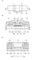
図1(A)は、半導体装置の上面図であり、図1(B)は、図1(A)に示す一点鎖線A1−A2の断面図であり、図1(C)は、図1(B)に示す半導体装置の一部の拡大図である。なお、図1(A)の上面図においては、図の明瞭化のために一部の要素を透過、または省いて図示している。 1A is a top view of the semiconductor device, FIG. 1B is a cross-sectional view along dashed-dotted line A1-A2 in FIG. 1A, and FIG. It is a one part enlarged view of the semiconductor device shown to B). Note that, in the top view of FIG. 1A, some elements are illustrated as being transparent or omitted for the sake of clarity.
図1(B)に示す半導体装置は、基板102上のゲート電極層104と、ゲート電極層104上のゲート絶縁層106と、ゲート絶縁層106上のソース電極層108及びドレイン電極層110と、ゲート絶縁層106、ソース電極層108、及びドレイン電極層110上の結晶部を含む酸化物半導体層112と、を有する。
A semiconductor device illustrated in FIG. 1B includes a
また、図1(B)に示す半導体装置は、ゲート絶縁層106、ソース電極層108、ドレイン電極層110、及び酸化物半導体層112上の第3の絶縁層114と、第3の絶縁層114上の第4の絶縁層116を含む構成としてもよい。
In addition, the semiconductor device illustrated in FIG. 1B includes a
なお、酸化物半導体層112において、酸化物半導体層112と、ソース電極層108、及びドレイン電極層110と、が接する領域にn型領域112aが形成されている。n型領域112aは、酸化物半導体層112のチャネル形成領域よりも抵抗が低い領域である。
Note that in the
チャネル形成領域は、ゲート絶縁層106と接する酸化物半導体層112に位置する。ゲート絶縁層106が酸化物半導体層112に接する面である第1の被形成面106aは、ソース電極層108が酸化物半導体層112に接する面である第2の被形成面108aと交差部122で交差する。また、第1の被形成面106aは、ドレイン電極層110が酸化物半導体層112に接する面である第3の被形成面110aと交差部124で交差する。なお、本明細書において、第1の被形成面、第2の被形成面、及び第3の被形成面それぞれは、酸化物半導体層が形成される面であり、平面だけでなく、曲面も含む。また、本明細書において、「交差する」とは、交差部で交差する面と面が作る角度が30°〜90°の範囲を意味する。
The channel formation region is located in the
酸化物半導体層112としては、例えばIn−M−Zn酸化物(MはAl、Ga、Ge、Y、Zr、Sn、La、Ce、またはHfの金属)を用いることができる。
As the
例えば、酸化物半導体層112としてIn:Ga:Zn=1:1:1または3:1:2の原子数比のIn−Ga−Zn酸化物を用いることができる。なお、酸化物半導体の原子数比は、誤差として上記の原子数比のプラスマイナス20%の変動を含む。なお、これらに限られず、必要とするトランジスタの半導体特性及び電気特性(電界効果移動度、しきい値電圧、ばらつき等)に応じて適切な組成のものを用いればよい。また、必要とするトランジスタの半導体特性を得るために、酸化物半導体のキャリア密度や不純物濃度、欠陥密度、金属元素と酸素の原子数比、原子間距離、密度等を適切なものとすることが好ましい。
For example, an In—Ga—Zn oxide with an atomic ratio of In: Ga: Zn = 1: 1: 1 or 3: 1: 2 can be used for the
また、酸化物半導体層112は、エネルギーギャップが2eV以上、好ましくは2.5eV以上、より好ましくは3eV以上である。このように、エネルギーギャップの広い酸化物半導体を用いることで、トランジスタのオフ電流を低減することができる。
The
また、酸化物半導体層112の厚さは、3nm以上200nm以下、好ましくは3nm以上100nm以下である。
The thickness of the
また、酸化物半導体層112において、第14族元素の一つであるシリコンや炭素が含まれると、酸化物半導体中の酸素欠損が増加し、n型化してしまう。
In addition, when the
また、酸化物半導体層112は、結晶部を含む。該結晶部を含む酸化物半導体は、例えば、CAAC(C Axis Aligned Crystal)を有する。別言すれば、結晶部を含む酸化物半導体層は、CAACを有する酸化物半導体を含む概念である。
The
CAACを有する酸化物半導体を、CAAC−OS(C Axis Aligned Crystalline Oxide Semiconductor)と呼ぶ。CAAC−OSは、完全な非晶質ではない。 An oxide semiconductor including a CAAC is referred to as a CAAC-OS (C Axis Crystalline Oxide Semiconductor). The CAAC-OS is not completely amorphous.
CAAC−OSは、例えば、透過型電子顕微鏡(TEM:Transmission Electron Microscope)による観察像で、結晶部を確認することができる場合がある。CAAC−OSに含まれる結晶部は、例えば、TEMによる観察像で、一辺100nmの立方体内に収まる大きさであることが多い。また、CAAC−OSは、TEMによる観察像で、結晶部と結晶部との境界を明確に確認できない場合がある。また、CAAC−OSは、TEMによる観察像で、粒界(グレインバウンダリーともいう。)を明確に確認できない場合がある。CAAC−OSは、例えば、明確な粒界を有さないため、不純物が偏析することが少ない。また、CAAC−OSは、例えば、明確な粒界を有さないため、欠陥準位密度が高くなることが少ない。また、CAAC−OSは、例えば、明確な粒界を有さないため、電子移動度の低下が小さい。 For example, the CAAC-OS may be able to confirm a crystal part in an observation image obtained by a transmission electron microscope (TEM: Transmission Electron Microscope). In many cases, a crystal part included in the CAAC-OS fits in a cube with a side of 100 nm, for example, as an observation image obtained by a TEM. In addition, in the CAAC-OS, there is a case where the boundary between the crystal part and the crystal part cannot be clearly confirmed in an observation image by TEM. In some cases, the CAAC-OS cannot clearly confirm a grain boundary (also referred to as a grain boundary) in an observation image obtained by a TEM. For example, the CAAC-OS does not have a clear grain boundary; In addition, since the CAAC-OS does not have a clear grain boundary, for example, the density of defect states is rarely increased. In addition, since the CAAC-OS does not have a clear grain boundary, for example, the decrease in electron mobility is small.
CAAC−OSは、例えば、複数の結晶部を有し、該複数の結晶部においてc軸が被形成面の法線ベクトルまたは表面の法線ベクトルに平行な方向に揃っている場合がある。また、CAAC−OSは、例えば、X線回折(XRD:X−Ray Diffraction)装置を用い、out−of−plane法による分析を行うと、配向を示す2θが31°近傍のピークが現れる場合がある。また、CAAC−OSは、例えば、電子線回折像で、スポット(輝点)が観測される場合がある。なお、特に、ビーム径が10nmφ以下、または5nmφ以下の電子線を用いて得られる電子線回折像を、極微電子線回折像と呼ぶ。また、CAAC−OSは、例えば、異なる結晶部間で、それぞれa軸およびb軸の向きが揃っていない場合がある。CAAC−OSは、例えば、c軸配向し、a軸または/およびb軸はマクロに揃っていない場合がある。 For example, the CAAC-OS includes a plurality of crystal parts, and the c-axis is aligned in a direction parallel to the normal vector of the surface to be formed or the normal vector of the surface in the plurality of crystal parts. In addition, when the CAAC-OS is analyzed by an out-of-plane method using, for example, an X-ray diffraction (XRD) apparatus, a peak where 2θ indicating orientation is near 31 ° may appear. is there. In the CAAC-OS, for example, spots (bright spots) may be observed in an electron diffraction pattern. In particular, an electron beam diffraction image obtained using an electron beam having a beam diameter of 10 nmφ or less or 5 nmφ or less is referred to as a micro electron beam diffraction image. In the CAAC-OS, for example, the directions of the a-axis and the b-axis may not be uniform between different crystal parts. For example, the CAAC-OS may be c-axis oriented and the a-axis and / or b-axis may not be aligned with the macro.
CAAC−OSに含まれる結晶部は、例えば、c軸がCAAC−OSの被形成面の法線ベクトルまたは表面の法線ベクトルに平行な方向になるように揃い、かつab面に垂直な方向から見て金属原子が三角形状または六角形状に配列し、c軸に垂直な方向から見て金属原子が層状または金属原子と酸素原子とが層状に配列している。なお、異なる結晶部間で、それぞれa軸およびb軸の向きが異なっていてもよい。本明細書において、単に垂直と記載する場合、80°以上100°以下、好ましくは85°以上95°以下の範囲も含まれることとする。また、単に平行と記載する場合、−10°以上10°以下、好ましくは−5°以上5°以下の範囲も含まれることとする。 The crystal part included in the CAAC-OS is aligned so that, for example, the c-axis is in a direction parallel to the normal vector of the formation surface of the CAAC-OS or the normal vector of the surface, and from a direction perpendicular to the ab plane. The metal atoms are arranged in a triangular shape or a hexagonal shape as viewed, and the metal atoms are arranged in layers or the metal atoms and oxygen atoms are arranged in layers as viewed from the direction perpendicular to the c-axis. Note that the directions of the a-axis and the b-axis may be different between different crystal parts. In this specification, the term “perpendicular” includes a range of 80 ° to 100 °, preferably 85 ° to 95 °. In addition, a simple term “parallel” includes a range of −10 ° to 10 °, preferably −5 ° to 5 °.
また、CAAC−OSは、例えば、欠陥準位密度を低減することで形成することができる。酸化物半導体において、例えば、酸素欠損は欠陥準位である。酸素欠損は、トラップ準位となることや、水素を捕獲することによってキャリア発生源となることがある。CAAC−OSを形成するためには、例えば、酸化物半導体に酸素欠損を生じさせないことが重要となる。従って、CAAC−OSは、欠陥準位密度の低い酸化物半導体である。または、CAAC−OSは、酸素欠損の少ない酸化物半導体である。 In addition, the CAAC-OS can be formed by reducing the density of defect states, for example. In an oxide semiconductor, for example, oxygen vacancies are defect levels. Oxygen deficiency may become a trap generation level or become a carrier generation source by capturing hydrogen. In order to form the CAAC-OS, for example, it is important to prevent oxygen vacancies from being generated in the oxide semiconductor. Therefore, the CAAC-OS is an oxide semiconductor with a low density of defect states. Alternatively, the CAAC-OS is an oxide semiconductor with few oxygen vacancies.
不純物濃度が低く、欠陥準位密度の低い(酸素欠損の少ない)ことを高純度真性または実質的に高純度真性と呼ぶ。高純度真性または実質的に高純度真性である酸化物半導体は、キャリア発生源が少ないため、キャリア密度を低くすることができる場合がある。従って、該酸化物半導体をチャネル形成領域に用いたトランジスタは、しきい値電圧がマイナスとなる電気特性(ノーマリーオンともいう。)になることが少ない場合がある。また、高純度真性または実質的に高純度真性である酸化物半導体は、欠陥準位密度が低いため、トラップ準位密度も低くなる場合がある。従って、該酸化物半導体をチャネル形成領域に用いたトランジスタは、電気特性の変動が小さく、信頼性の高いトランジスタとなる場合がある。なお、酸化物半導体のトラップ準位に捕獲された電荷は、消失するまでに要する時間が長く、あたかも固定電荷のように振る舞うことがある。そのため、トラップ準位密度の高い酸化物半導体をチャネル形成領域に用いたトランジスタは、電気特性が不安定となる場合がある。 A low impurity concentration and a low defect level density (small oxygen vacancies) is called high purity intrinsic or substantially high purity intrinsic. An oxide semiconductor that is highly purified intrinsic or substantially highly purified intrinsic has few carrier generation sources, and thus may have a low carrier density. Therefore, a transistor in which the oxide semiconductor is used for a channel formation region may rarely have electrical characteristics (also referred to as normally-on) in which the threshold voltage is negative. In addition, a highly purified intrinsic or substantially highly purified intrinsic oxide semiconductor has a low density of defect states, and thus may have a low density of trap states. Therefore, a transistor in which the oxide semiconductor is used for a channel formation region may have a small change in electrical characteristics and be a highly reliable transistor. Note that the charge trapped in the trap level of the oxide semiconductor takes a long time to disappear, and may behave as if it were a fixed charge. Therefore, a transistor in which an oxide semiconductor with a high trap state density is used for a channel formation region may have unstable electric characteristics.
また、高純度真性または実質的に高純度真性であるCAAC−OSを用いたトランジスタは、可視光や紫外光の照射による電気特性の変動が小さい。 In addition, a transistor using a high-purity intrinsic or substantially high-purity intrinsic CAAC-OS has little variation in electrical characteristics due to irradiation with visible light or ultraviolet light.
なお、CAAC−OSに限らず、何らかの結晶性を有する酸化物半導体を用いてもよい。 Note that an oxide semiconductor having some crystallinity may be used instead of the CAAC-OS.
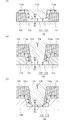
ここで、酸化物半導体層112中に形成されるn型領域112aについて、図7及び図8に示す、本発明の一態様の半導体装置と比較するための構成の半導体装置を用いて説明する。
Here, the n-
図7(A)に示す半導体装置は、ボトムゲートトップコンタクト構造のトランジスタである。図7(A)は、トランジスタの断面図を示し、図7(B)、(C)は、図7(A)に示すトランジスタの一部の拡大図である。なお、図7に示す半導体装置の上面図は、図1(A)に示す半導体装置の上面図と概略同じであるため、ここでの説明は省略する。 The semiconductor device illustrated in FIG. 7A is a bottom-gate top-contact transistor. 7A illustrates a cross-sectional view of the transistor, and FIGS. 7B and 7C are enlarged views of part of the transistor illustrated in FIG. 7A. Note that the top view of the semiconductor device illustrated in FIG. 7 is substantially the same as the top view of the semiconductor device illustrated in FIG. 1A; therefore, description thereof is omitted here.
図7(A)に示す半導体装置は、基板202上のゲート電極層204と、ゲート電極層204上のゲート絶縁層206と、ゲート絶縁層206上のソース電極層208及びドレイン電極層210と、ゲート絶縁層206、ソース電極層208、及びドレイン電極層210上の結晶部を含む酸化物半導体層212と、を有する。
A semiconductor device illustrated in FIG. 7A includes a
また、図7(A)に示す半導体装置は、ゲート絶縁層206、ソース電極層208、ドレイン電極層210、及び酸化物半導体層212上の第3の絶縁層214と、第3の絶縁層214上の第4の絶縁層216を含む構成としてもよい。
7A, the third insulating
なお、酸化物半導体層212において、酸化物半導体層212と、ソース電極層208、及びドレイン電極層210と、が接する領域にn型領域212aが形成されている。n型領域212aは、酸化物半導体層212のチャネル形成領域よりも抵抗が低い領域である。
Note that in the
また、図7及び図8に示す酸化物半導体層212としては、図1に示す酸化物半導体層112と同様の材料、または非晶質の酸化物半導体層を用いることができる。
7 and 8 can be formed using a material similar to that of the
酸化物半導体層212中のn型領域212aは、ソース電極層208及びドレイン電極層210の形成のためのスパッタリングによるダメージや、ソース電極層208及びドレイン電極層210形成後の熱処理等により形成される(図7(B)参照)。別言すれば、n型領域212aは、ソース電極層208及びドレイン電極層210が酸化物半導体層212と接触する部分に形成される。
The n-
n型領域212aの形状は、トランジスタやその周辺構造の材料や設計、及び作製条件等に依存する。このため、例えばn型領域212aが横方向に拡がり過ぎた場合や、チャネル長を短く設計した場合には、ソース電極層208下のn型領域212aと、ドレイン電極層210の下のn型領域212aとが近接することとなる。
The shape of the n-
とくに、酸化物半導体層212が非晶質構造の酸化物半導体層の場合、酸化物半導体層212中に結晶部を有さないため、n型領域212aが拡がりやすい。また、酸化物半導体層212がCAAC−OSである場合、c軸に垂直な方向から見て金属原子が層状または金属原子と酸素原子とが層状に配列している結晶部を有するため、a軸またはb軸にn型領域212aが拡がる可能性がある。
In particular, in the case where the
酸化物半導体層212中のn型領域212aが拡がった場合、ソース電極層208下のn型領域212aとドレイン電極層210下のn型領域212aとが完全に接触することがなくても、設計時のチャネル長(L長)とトランジスタ作製後のL長が異なってしまう。
In the case where the n-
例えばソース電極層208及びドレイン電極層210にチタンを用いた場合にチタンがウィスカー状(髭状)に成長する(図7(C)中の矢印参照)。
For example, when titanium is used for the
また、設計時のL長が短い場合、すなわちソース電極層208とドレイン電極層210との間隔が短い場合、n型領域212aは、ソース電極層208とドレイン電極層210とを電気的に接続させてしまい、所望のトランジスタ特性を得ることができなくなってしまう。
When the L length at the time of design is short, that is, when the distance between the
そこで、図8(A)または図8(B)に示すように、n型領域212aの一部をエッチングすることによって、酸化物半導体層212に凹部を設けることで、n型領域212aが電気的に接続されるおそれを抑制することが可能となる。なお、n型領域212aの一部を除去するエッチングは、ソース電極層208及びドレイン電極層210を形成する際のエッチング時、またはソース電極層208及びドレイン電極層210形成後の処理(例えば、プラズマ処理または希フッ酸処理によるウエットエッチング処理等)によって、行うことができる。
Thus, as illustrated in FIG. 8A or FIG. 8B, the n-
しかしながら、酸化物半導体層212に凹部を設ける構成においては、基板面内で均一にエッチング量を調整し、酸化物半導体層212のチャネル形成領域の膜厚を揃える必要があり、基板面内で酸化物半導体層212の膜厚に、ばらつきが生じてしまう。
However, in the structure in which the
従って、酸化物半導体層212中に形成されるn型領域212aは、深さ方向すなわち酸化物半導体層212の膜厚方向に形成させ、横方向へ拡がるのを抑制させた構成が望ましい。
Therefore, the n-
n型領域の横方向への拡がりを抑制させた構成としては、図1(B)に示すように、結晶部を含む酸化物半導体層112と、酸化物半導体層112に接するソース電極層108及びドレイン電極層110と、を有し、酸化物半導体層112は、チャネル形成領域と、ソース電極層108及びドレイン電極層110と接するn型領域112aと、を有し、チャネル形成領域と、n型領域112aで、結晶部の結晶方向が異なる構成である。
As a structure in which the lateral extension of the n-type region is suppressed, as illustrated in FIG. 1B, the
別言すれば、n型領域の横方向への拡がりを抑制させた構成としては、図1(B)に示すように、結晶部を含む酸化物半導体層112と、酸化物半導体層112に接するソース電極層108及びドレイン電極層110と、を有し、酸化物半導体層112は、チャネル形成領域と、ソース電極層108及びドレイン電極層110と接するn型領域112aと、を有し、ゲート絶縁層106が酸化物半導体層112に接する面である第1の被形成面106aは、ソース電極層108が酸化物半導体層112に接する面である第2の被形成面108aと交差部122で交差し、第1の被形成面106aは、ドレイン電極層110が酸化物半導体層112に接する面である第3の被形成面110aと交差部124で交差する構成である。なお、このような構成とすることにより、チャネル形成領域と、n型領域112aで、結晶部の結晶方向が異なることになる。
In other words, as a structure in which the lateral extension of the n-type region is suppressed, the
ここで、図1(C)を用いて、酸化物半導体層112の結晶部の結晶方向について説明を行う。
Here, the crystal direction of the crystal part of the
なお、図1(C)は、図1(B)に示す半導体装置の酸化物半導体層112周辺の拡大図を表している。酸化物半導体層112は、ゲート絶縁層106、ソース電極層108、及びドレイン電極層110で形成された凹部に沿って形成される。別言すれば、凹部は第1の被形成面106a、第2の被形成面108a、及び第3の被形成面110aを有し、第1の被形成面106a、第2の被形成面108a、及び第3の被形成面110a上に酸化物半導体層112が形成される。酸化物半導体層112の結晶部は、図1(C)の矢印の方向にc軸が配向している。図1(C)の矢印の方向は、ゲート絶縁層106の上面の第1の被形成面106aに接する酸化物半導体層112では第1の被形成面106aと垂直方向であり、ソース電極層108の側面の第2の被形成面108aに接する酸化物半導体層112では第2の被形成面108aと垂直方向であり、ドレイン電極層110の側面の第3の被形成面110aに接する酸化物半導体層112では第3の被形成面110aと垂直方向であり、ソース電極層108及びドレイン電極層110の上面に接する酸化物半導体層112では当該上面と垂直方向である。なお、ここでは結晶部を含む酸化物半導体層112は、先に説明したCAAC−OSとする。
Note that FIG. 1C illustrates an enlarged view around the
また、図1(C)に示すように、酸化物半導体層112中に形成されるn型領域112aは、ソース電極層108及びドレイン電極層110が接触した領域に形成される。酸化物半導体層112が、ゲート絶縁層106、ソース電極層108、及びドレイン電極層110で形成された凹部に沿って形成されているため、n型領域112aも該凹部に沿った形状に形成される。すなわち、ソース電極層108の側面の第2の被形成面108a、及びドレイン電極層110の側面の第3の被形成面110aに形成されるn型領域112aの結晶部の結晶方向が、ゲート絶縁層106の上面の第1の被形成面106aに形成されるチャネル形成領域の結晶部の結晶方向と異なる。従って、酸化物半導体層112のチャネル形成領域と、n型領域112aで、結晶部の結晶方向を異なる構造とすることができる。
In addition, as illustrated in FIG. 1C, the n-
ただし、図1(C)に示す構造においては、n型領域112aの結晶部の結晶方向は、n型領域112aの一部の領域、具体的には、ソース電極層108の上面側、及びドレイン電極層110上面側の領域がチャネル形成領域と結晶方向が同じである。しかし、隣接した領域にチャネル形成領域と結晶部の結晶方向が異なる領域を有するため、n型領域112aの横方向への拡がりを抑制することができる。
However, in the structure illustrated in FIG. 1C, the crystal direction of the crystal part of the n-
例えば、n型領域112aは、ソース電極層108及びドレイン電極層110に接する酸化物半導体層112に、結晶部のc軸が配向した方向に垂直方向に拡がる傾向があるため、ソース電極層108及びドレイン電極層110に接する酸化物半導体層112のc軸とチャネル形成領域のc軸を異なる方向に配向させることにより、n型領域112aのチャネル形成領域への拡がりを抑制することができる。
For example, the n-
このように、本発明の一態様は、チャネル形成領域と結晶方向が異なる領域が、n型領域112a中に少なくとも一部に形成されていればよい。
As described above, according to one embodiment of the present invention, a region whose crystal direction is different from that of the channel formation region only needs to be formed in at least part of the n-
なお、本実施の形態において、チャネル形成領域とは、ゲート電極層104に重畳して設けられた酸化物半導体層112中のソース電極層108とドレイン電極層110との間の領域をいう。ただし、図1(B)、(C)に示すように、酸化物半導体層112中にn型領域112aを含む場合においては、ゲート電極層104に重畳して設けられた酸化物半導体層112中のn型領域112aに挟まれた領域がチャネル形成領域となる。このように、チャネル形成領域は、酸化物半導体層112の半導体特性に依存する。従って、ゲート電極層104に重畳して設けられた酸化物半導体層112は、その半導体特性がi型の場合にはチャネル形成領域となり、n型の場合にはチャネル形成領域とならない。また、チャネルとは、チャネル形成領域において、電流が主として流れる領域をいう。例えば、図1(C)において、チャネルは、ゲート電極層104に重畳して形成された酸化物半導体層112のn型領域112a間であり、且つゲート絶縁層106の近傍の領域をいう。また、チャネル長(L長)は、図1(C)に示すLの長さとなる。
Note that in this embodiment, the channel formation region refers to a region between the
このように、酸化物半導体層112中のチャネル形成領域と、ソース電極層108及びドレイン電極層110が接する酸化物半導体層112中のn型領域112aとで、結晶部の結晶方向を異ならせることによって、酸化物半導体層112に形成されるn型領域112aの横方向への拡がりを抑制することができる。従って、チャネル長(L長)は、設計時におけるチャネル長であるソース電極層108とドレイン電極層110との間の距離に概略等しくすることができる。
In this manner, the crystal direction of the crystal part is different between the channel formation region in the
次に、図1に示す本発明の一態様の半導体装置のその他の構成について、以下説明を行う。 Next, another structure of the semiconductor device of one embodiment of the present invention illustrated in FIG. 1 is described below.
基板102としては、アルミノシリケートガラス、アルミノホウケイ酸ガラス、バリウムホウケイ酸ガラスなどのガラス材料を用いる。量産する上では、基板102は、第8世代(2160mm×2460mm)、第9世代(2400mm×2800mm、または2450mm×3050mm)、第10世代(2950mm×3400mm)等のマザーガラスを用いることが好ましい。マザーガラスは、処理温度が高く、処理時間が長いと大幅に収縮するため、マザーガラスを使用して量産を行う場合、作製工程の加熱処理は、好ましくは600℃以下、さらに好ましくは450℃以下、さらに好ましくは350℃以下とすることが望ましい。
As the
ゲート電極層104としては、アルミニウム、クロム、銅、タンタル、チタン、モリブデン、タングステンから選ばれた金属元素、または上述した金属元素を成分とする合金か、上述した金属元素を組み合わせた合金等を用いて形成することができる。また、ゲート電極層104は、単層構造でも、二層以上の積層構造としてもよい。例えば、シリコンを含むアルミニウム膜の単層構造、アルミニウム膜上にチタン膜を積層する二層構造、窒化チタン膜上にチタン膜を積層する二層構造、窒化チタン膜上にタングステン膜を積層する二層構造、窒化タンタル膜または窒化タングステン膜上にタングステン膜を積層する二層構造、チタン膜と、そのチタン膜上にアルミニウム膜を積層し、さらにその上にチタン膜を形成する三層構造等がある。また、アルミニウムに、チタン、タンタル、タングステン、モリブデン、クロム、ネオジム、スカンジウムから選ばれた元素の膜、または複数組み合わせた合金膜、もしくは窒化膜を用いてもよい。
As the
ゲート絶縁層106としては、例えば酸化シリコン膜、酸化窒化シリコン膜、窒化酸化シリコン膜、窒化シリコン膜、酸化アルミニウム膜、窒化シリコン膜、窒化酸化シリコン膜などを用いればよく、積層または単層で設ける。
As the
また、ゲート絶縁層106を積層構造とし、第1の窒化シリコン膜として、欠陥が少ない窒化シリコン膜とし、第1の窒化シリコン膜上に、第2の窒化シリコン膜として、水素放出量及びアンモニア放出量の少ない窒化シリコン膜を設け、第2の窒化シリコン膜上に酸化絶縁膜を設けることで、ゲート絶縁層106として、欠陥が少なく、且つ水素及びアンモニアの放出量の少ないゲート絶縁層106を形成することができる。この結果、ゲート絶縁層106に含まれる水素及び窒素が、酸化物半導体層112への移動を抑制することが可能である。例えば、ゲート絶縁層106として、325nmの窒化シリコン膜と、50nmの酸化シリコン膜との積層構造を用いることができる。
In addition, the
また、ゲート絶縁層106に窒化シリコン膜を用いることで、以下の効果を得ることができる。窒化シリコン膜は、酸化シリコン膜と比較して比誘電率が高く、同等の静電容量を得るのに必要な膜厚が大きいため、ゲート絶縁層を物理的に厚膜化することができる。よって、トランジスタの絶縁耐圧の低下を抑制、さらには絶縁耐圧を向上させて、トランジスタの静電破壊を抑制することができる。
In addition, by using a silicon nitride film for the
ゲート絶縁層106の厚さは、5nm以上500nm以下、より好ましくは10nm以上450nm以下、より好ましくは50nm以上400nm以下とするとよい。
The thickness of the
ソース電極層108及びドレイン電極層110としては、導電材料として、アルミニウム、チタン、クロム、ニッケル、銅、イットリウム、ジルコニウム、モリブデン、銀、タンタル、またはタングステンからなる単体金属、またはこれを主成分とする合金を単層構造または積層構造として用いる。例えば、アルミニウム膜の単層構造、アルミニウム膜上にチタン膜を積層する二層構造、タングステン膜上にチタン膜を積層する二層構造、銅−マグネシウム−アルミニウム合金膜上に銅膜を積層する二層構造、チタン膜または窒化チタン膜と、そのチタン膜または窒化チタン膜上に重ねてアルミニウム膜または銅膜を積層し、さらにその上にチタン膜または窒化チタン膜を形成する三層構造、モリブデン膜または窒化モリブデン膜と、そのモリブデン膜または窒化モリブデン膜上に重ねてアルミニウム膜または銅膜を積層し、さらにその上にモリブデン膜または窒化モリブデン膜を形成する三層構造等がある。なお、ソース電極層108及びドレイン電極層110として、酸化インジウム、酸化錫または酸化亜鉛を含む透明導電材料を用いてもよい。
The
第3の絶縁層114としては、酸化物半導体層112として用いる酸化物半導体との界面特性を向上させるため、無機材料の酸化物絶縁膜を用いることが好ましく、例えば酸素または窒素を含むシリコン膜を用いることができる。とくに、第3の絶縁層114としては、化学量論的組成を満たす酸素よりも多くの酸素を含む酸化シリコン膜を用いると好ましい。例えば、第3の絶縁層114としては、厚さ150nm以上400nm以下の酸化シリコン膜、酸化窒化シリコン膜等を用いることができる。
As the third insulating
第4の絶縁層116は、酸化物半導体層112として用いる酸化物半導体への水分浸入を防止するブロック層としての機能を有する。第4の絶縁層116としては、例えば窒化シリコン膜、窒化酸化シリコン膜などを用いることができる。また、窒化シリコン膜を用いた場合、緻密性を高めるために、高温で成膜されることが好ましく、例えば基板温度350℃での成膜が考えられる。また、第4の絶縁層116として、高温で成膜する窒化シリコン膜を用いる場合は、酸化物半導体層112として用いる酸化物半導体から酸素が脱離し、キャリア濃度が上昇する現象が発生することがあるため、このような現象が発生しない温度が上限とする。
The fourth insulating
第3の絶縁層114及び第4の絶縁層116の構成としては、例えば、酸化窒化シリコン膜と、窒化シリコン膜との積層構造とすることができる。より具体的には、酸化窒化シリコン膜300nm上に窒化シリコン膜150nmを積層する構造などである。このとき、酸化窒化シリコン膜は、例えば、ソース電極層108及びドレイン電極層110の段差被覆部分の被覆形状が悪く、鬆があっても窒化シリコン膜によって鬆を良好に被覆することができるので好適である。
For example, the third insulating
以上が本発明の一態様における半導体装置である。本発明の一態様の半導体装置は、酸化物半導体を用いた半導体装置において、チャネル形成領域中に酸素欠損が少ない新規な半導体装置を提供することができる。また、本発明の一態様の半導体装置は、酸化物半導体を用いた半導体装置において、チャネル長の縮小を抑制した新規な半導体装置を提供することができる。 The above is the semiconductor device of one embodiment of the present invention. The semiconductor device of one embodiment of the present invention can provide a novel semiconductor device with less oxygen vacancies in a channel formation region in an oxide semiconductor. Further, the semiconductor device of one embodiment of the present invention can provide a novel semiconductor device in which reduction in channel length is suppressed in a semiconductor device including an oxide semiconductor.
なお、本実施の形態は、本明細書で示す他の実施の形態と適宜組み合わせることができる。 Note that this embodiment can be combined with any of the other embodiments described in this specification as appropriate.
(実施の形態2)
本実施の形態では、実施の形態1に示す半導体装置の作製方法について、図1(B)を用いて以下説明する。また、実施の形態1で説明した機能と同様の機能を有する部分については、同様の符号を付し、その詳細な説明は省略する。
(Embodiment 2)
In this embodiment, a method for manufacturing the semiconductor device described in
まず、基板102を準備する。その後、基板102上に導電膜を成膜し、該導電膜を所望の領域に加工することで、ゲート電極層104を形成する。その後、基板102、及びゲート電極層104上にゲート絶縁層106を形成する。なお、基板102、ゲート電極層104、及びゲート絶縁層106としては、先に説明した材料を用いることができる。本実施の形態においては、基板102としては、ガラス基板を用いる。また、ゲート電極層104としては、スパッタリング法を用い、膜厚100nmのタングステン膜を形成する。また、ゲート絶縁層106としては、PE−CVD法を用い、膜厚350nmの窒化シリコン膜と、膜厚50nmの酸化窒化シリコン膜を形成する。
First, the
次に、ゲート絶縁層106上に導電膜を成膜し、該導電膜を所望の領域に加工することで、ソース電極層108及びドレイン電極層110を形成する。ソース電極層108、及びドレイン電極層110としては、先に説明した材料を用いることができる。本実施の形態においては、ソース電極層108及びドレイン電極層110としては、スパッタリング法を用い、膜厚50nmのタングステン膜と、膜厚400nmのアルミニウム膜と、膜厚100nmのチタン膜を形成する。
Next, a conductive film is formed over the
次に、ゲート絶縁層106、ソース電極層108及びドレイン電極層110上に酸化物半導体膜を成膜し、該酸化物半導体膜を所望の領域に加工することで、酸化物半導体層112を形成する。これにより、酸化物半導体層112は、チャネル形成領域と、ソース電極層108及びドレイン電極層110と接するn型領域112aと、を有し、チャネル形成領域は、ゲート絶縁層106と接する酸化物半導体層112に位置する。ゲート絶縁層106が酸化物半導体層112に接する面である第1の被形成面106aは、ソース電極層108が酸化物半導体層112に接する面である第2の被形成面108aと交差部122で交差し、第1の被形成面106aは、ドレイン電極層110が酸化物半導体層112に接する面である第3の被形成面110aと交差部124で交差する。酸化物半導体層112としては、先に説明した材料を用いることができる。本実施の形態においては、酸化物半導体層112としては、スパッタリング法を用い、膜厚35nmのIn−Ga−Zn系酸化物であるIGZO膜を形成する。なお、IGZO膜の組成は、原子数比でIn:Ga:Zn=1:1:1のターゲットを用いる。
Next, an oxide semiconductor film is formed over the
また、酸化物半導体層112として、CAAC−OSを用いる場合、以下の条件を適用することが好ましい。
In the case where a CAAC-OS is used as the
成膜時の基板温度を高くすることが好ましい。例えば、基板加熱温度を100℃以上740℃以下、好ましくは100℃以上500℃以下、さらに好ましくは150℃以上450℃以下として酸化物半導体を成膜することによりCAAC−OSを形成することができる。 It is preferable to increase the substrate temperature during film formation. For example, the CAAC-OS can be formed by forming an oxide semiconductor with a substrate heating temperature of 100 ° C to 740 ° C, preferably 100 ° C to 500 ° C, more preferably 150 ° C to 450 ° C. .
例えば、不純物濃度を低減させてCAAC−OSを形成することにより、不純物による酸化物半導体の結晶状態の崩壊を抑制することができる。例えば、スパッタリング装置の成膜室内に存在する不純物(水素、水、二酸化炭素、及び窒素など)を低減することが好ましい。また、成膜ガス中の不純物を低減することが好ましい。例えば、成膜ガスとして露点が−80℃以下、さらには−100℃以下である成膜ガスを用いることが好ましい。 For example, the CAAC-OS is formed with a reduced impurity concentration, whereby the collapse of the crystal state of the oxide semiconductor due to the impurities can be suppressed. For example, it is preferable to reduce impurities (such as hydrogen, water, carbon dioxide, and nitrogen) present in the deposition chamber of the sputtering apparatus. Further, it is preferable to reduce impurities in the deposition gas. For example, it is preferable to use a film forming gas having a dew point of −80 ° C. or lower, more preferably −100 ° C. or lower as the film forming gas.
また、成膜ガス中の酸素割合を高め、電力を最適化することで成膜時のプラズマダメージを軽減すると好ましい。成膜ガス中の酸素割合は、30体積%以上、好ましくは100体積%とする。 In addition, it is preferable to reduce plasma damage during film formation by increasing the oxygen ratio in the film formation gas and optimizing electric power. The oxygen ratio in the deposition gas is 30% by volume or more, preferably 100% by volume.
CAAC−OSを成膜した後、加熱処理を行ってもよい。加熱処理の温度は、100℃以上740℃以下、好ましくは200℃以上500℃以下とする。また、加熱処理の時間は1分以上24時間以下、好ましくは6分以上4時間以下とする。また、加熱処理は、不活性雰囲気または酸化性雰囲気で行えばよい。好ましくは、不活性雰囲気で加熱処理を行った後、酸化性雰囲気で加熱処理を行う。不活性雰囲気での加熱処理により、CAAC−OSの不純物濃度を短時間で低減することができる。一方、不活性雰囲気での加熱処理によりCAAC−OSに酸素欠損が生成されることがある。その場合、酸化性雰囲気での加熱処理によって該酸素欠損を低減することができる。また、加熱処理を行うことで、CAAC−OSの結晶性をさらに高めることができる。なお、加熱処理は1000Pa以下、100Pa以下、10Pa以下または1Pa以下の減圧下で行ってもよい。減圧下では、CAAC−OSの不純物濃度をさらに短時間で低減することができる。 Heat treatment may be performed after the CAAC-OS is formed. The temperature of the heat treatment is 100 ° C. or higher and 740 ° C. or lower, preferably 200 ° C. or higher and 500 ° C. or lower. The heat treatment time is 1 minute to 24 hours, preferably 6 minutes to 4 hours. Further, the heat treatment may be performed in an inert atmosphere or an oxidizing atmosphere. Preferably, after heat treatment in an inert atmosphere, heat treatment is performed in an oxidizing atmosphere. By the heat treatment in an inert atmosphere, the impurity concentration of the CAAC-OS can be reduced in a short time. On the other hand, oxygen vacancies may be generated in the CAAC-OS by heat treatment in an inert atmosphere. In that case, the oxygen vacancies can be reduced by heat treatment in an oxidizing atmosphere. Further, the crystallinity of the CAAC-OS can be further increased by performing the heat treatment. Note that the heat treatment may be performed under a reduced pressure of 1000 Pa or less, 100 Pa or less, 10 Pa or less, or 1 Pa or less. Under reduced pressure, the impurity concentration of CAAC-OS can be further reduced in a short time.
以上により作製したCAAC−OS中の水素濃度は、二次イオン質量分析(SIMS:Secondary Ion Mass Spectrometry)において、2×10²⁰atoms/cm3以下、好ましくは5×1019atoms/cm3以下、より好ましくは1×1019atoms/cm3以下、さらに好ましくは5×1018atoms/cm3以下とすることができる。 The hydrogen concentration in the CAAC-OS produced as described above is 2 × 10 20 atoms / cm 3 or less, preferably 5 × 10 19 atoms / cm 3 or less, in secondary ion mass spectrometry (SIMS). More preferably, it may be 1 × 10 19 atoms / cm 3 or less, and further preferably 5 × 10 18 atoms / cm 3 or less.
また、以上により作製したCAAC−OS中の窒素濃度は、SIMSにおいて、5×10¹⁹atoms/cm3未満、好ましくは5×1018atoms/cm3以下、より好ましくは1×1018atoms/cm3以下、さらに好ましくは5×1017atoms/cm3以下とすることができる。 Further, the nitrogen concentration in the CAAC-OS manufactured as described above is less than 5 × 10 19 atoms / cm 3 , preferably 5 × 10 18 atoms / cm 3 or less, more preferably 1 × 10 18 atoms / cm 3 in SIMS. 3 or less, more preferably 5 × 10 17 atoms / cm 3 or less.
また、以上により作製したCAAC−OS中の炭素濃度は、SIMSにおいて、5×10¹⁹atoms/cm3未満、好ましくは5×1018atoms/cm3以下、より好ましくは1×1018atoms/cm3以下、さらに好ましくは5×1017atoms/cm3以下とすることができる。 The carbon concentration in the CAAC-OS manufactured as described above is less than 5 × 10 19 atoms / cm 3 , preferably 5 × 10 18 atoms / cm 3 or less, more preferably 1 × 10 18 atoms / cm 3 in SIMS. 3 or less, more preferably 5 × 10 17 atoms / cm 3 or less.
また、以上により作製したCAAC−OS中のシリコン濃度は、SIMSにおいて、5×10¹⁹atoms/cm3未満、好ましくは5×1018atoms/cm3以下、より好ましくは1×1018atoms/cm3以下、さらに好ましくは5×1017atoms/cm3以下とすることができる。 The silicon concentration in the CAAC-OS manufactured as described above is less than 5 × 10 19 atoms / cm 3 , preferably 5 × 10 18 atoms / cm 3 or less, more preferably 1 × 10 18 atoms / cm 3 in SIMS. 3 or less, more preferably 5 × 10 17 atoms / cm 3 or less.
また、以上により作製したCAAC−OSは、昇温脱離ガス分光法(TDS:Thermal Desorption Spectroscopy)分析によるm/zが2(水素分子など)である気体分子(原子)、m/zが18である気体分子(原子)、m/zが28である気体分子(原子)及びm/zが44である気体分子(原子)の放出量が、それぞれ1×1019個/cm3以下、好ましくは1×1018個/cm3以下とすることができる。 In addition, the CAAC-OS manufactured as described above has a gas molecule (atom) in which m / z is 2 (hydrogen molecule or the like) by a temperature desorption gas spectroscopy (TDS) analysis, and an m / z is 18 Gas molecules (atoms) having an m / z of 28 and gas molecules (atoms) having an m / z of 44 are each released in an amount of 1 × 10 19 atoms / cm 3 or less, preferably Can be 1 × 10 18 pieces / cm 3 or less.
以上のようにして、CAAC−OSを形成することができる。該CAAC−OSを、酸化物半導体層112として好適に用いることができる。
As described above, the CAAC-OS can be formed. The CAAC-OS can be preferably used as the
なお、酸化物半導体層112を形成した後、膜中の水素や水分を除去するために熱処理を行うことが好ましい。例えば、脱水や脱水素のために、窒素雰囲気で450℃1時間の熱処理、または350℃1時間の熱処理を行うとよい。
Note that after the
また、酸化物半導体層112として酸化物半導体を用いた場合、該酸化物半導体中の酸素欠損を低減させるため、例えば窒素及び酸素雰囲気で450℃1時間、または窒素及び酸素雰囲気で350℃1時間などの熱処理をさらに行うとよい。
In the case where an oxide semiconductor is used for the
次に、ゲート絶縁層106、ソース電極層108、ドレイン電極層110、及び酸化物半導体層112上に第3の絶縁層114及び第4の絶縁層116を形成する。なお、第3の絶縁層114及び第4の絶縁層116としては、先に説明した材料を用いることができる。本実施の形態においては、第3の絶縁層114としては、PE−CVD法を用い、膜厚450nmの酸化窒化シリコン膜を用いる。また、第4の絶縁層116としては、PE−CVD法を用い、膜厚100nmの窒化シリコン膜を用いる。
Next, the third insulating
以上により図1(B)に示す本発明の一態様の半導体装置を作製することができる。 Through the above steps, the semiconductor device of one embodiment of the present invention illustrated in FIG. 1B can be manufactured.
なお、本実施の形態は、本明細書で示す他の実施の形態と適宜組み合わせることができる。 Note that this embodiment can be combined with any of the other embodiments described in this specification as appropriate.
(実施の形態3)
本実施の形態では、実施の形態1に示す半導体装置の変形例について、図2及び図3を用いて説明する。
(Embodiment 3)
In this embodiment, a modified example of the semiconductor device described in
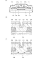
図2(A)は、半導体装置の断面図であり、図2(B)は、図2(A)に示す半導体装置の一部の拡大図である。なお、図2に示す半導体装置の上面図については、図1(A)に示す半導体装置と概略同等の上面図となるため、ここでは省略する。また、実施の形態1で説明した機能と同様の機能を有する部分については、同様の符号を付し、その詳細な説明は省略する。
2A is a cross-sectional view of the semiconductor device, and FIG. 2B is an enlarged view of a part of the semiconductor device illustrated in FIG. Note that the top view of the semiconductor device illustrated in FIG. 2 is substantially the same as the top view of the semiconductor device illustrated in FIG. Further, portions having the same functions as those described in
図2(A)に示す半導体装置は、基板102上のゲート電極層104と、ゲート電極層104上のゲート絶縁層106と、ゲート絶縁層106上の第1の絶縁層118a及び第2の絶縁層118bと、ゲート絶縁層106、第1の絶縁層118a、及び第2の絶縁層118bによって形成された凹部と、凹部に沿って形成された結晶部を含む酸化物半導体層112と、第1の絶縁層118a、第2の絶縁層118b、及び酸化物半導体層112上のソース電極層108及びドレイン電極層110と、を有する。
A semiconductor device illustrated in FIG. 2A includes a
別言すれば、図2(A)に示す半導体装置は、ゲート絶縁層106、第1の絶縁層118a、及び第2の絶縁層118b上の結晶部を含む酸化物半導体層112と、第1の絶縁層118a、及び酸化物半導体層112上のソース電極層108と、第2の絶縁層118b、及び酸化物半導体層112上のドレイン電極層110と、を有し、ゲート絶縁層106が酸化物半導体層112に接する面である第1の被形成面106aは、第1の絶縁層118aが酸化物半導体層112に接する面である第2の被形成面118a1と交差部126で交差し、第1の被形成面106aは、第2の絶縁層118bが酸化物半導体層112に接する面である第3の被形成面118b1と交差部128で交差する。
In other words, the semiconductor device illustrated in FIG. 2A includes the
また、図2(A)に示す半導体装置は、ゲート絶縁層106、ソース電極層108、ドレイン電極層110、及び酸化物半導体層112上の第3の絶縁層114と、第3の絶縁層114上の第4の絶縁層116を含む構成としてもよい。
2A includes a third
なお、酸化物半導体層112において、酸化物半導体層112と、ソース電極層108、及びドレイン電極層110と、が接する領域にn型領域112aが形成されている。
Note that in the
図2(A)に示す半導体装置は、実施の形態1の図1(B)に示す半導体装置と異なる点として、第1の絶縁層118a及び第2の絶縁層118bが形成されている。また、図2(A)に示す半導体装置は、酸化物半導体層112と接触するソース電極層108及びドレイン電極層110の位置が異なる。図1(B)に示す半導体装置においては、酸化物半導体層112の下部において、ソース電極層108及びドレイン電極層110が酸化物半導体層112と接触していたが、図2(A)に示す半導体装置においては、酸化物半導体層112の上部において、ソース電極層108及びドレイン電極層110が酸化物半導体層112と接触している。従って、酸化物半導体層112中に形成されるn型領域112aの位置も異なる。
The semiconductor device illustrated in FIG. 2A is different from the semiconductor device illustrated in FIG. 1B of
なお、第1の絶縁層118a及び第2の絶縁層118bとしては、ゲート絶縁層106で用いることのできる材料と同様の材料を用いることができる。また、第1の絶縁層118a及び第2の絶縁層118bの一部は、ゲート絶縁層の一部としても機能することができる。
Note that the first insulating
ここで、図2(B)に図2(A)に示す半導体装置の酸化物半導体層112周辺の拡大図を示す。
Here, FIG. 2B is an enlarged view around the
図2(B)に示すように、結晶部を含む酸化物半導体層112は、ゲート絶縁層106、第1の絶縁層118a、及び第2の絶縁層118bで形成された凹部に沿って形成される。つまり、酸化物半導体層112は、第1の被形成面106a、第2の被形成面118a1、及び第3の被形成面118b1上に形成される。酸化物半導体層112の結晶部は、図2(B)の矢印の方向にc軸が配向している。図2(B)に示す矢印の方向は、第1の被形成面106a、第2の被形成面118a1、及び第3の被形成面118b1それぞれに垂直方向である。なお、ここでは結晶部を含む酸化物半導体層112は、先に説明したCAAC−OSとする。
As illustrated in FIG. 2B, the
また、図2(B)に示すように、酸化物半導体層112中に形成されるn型領域112aは、ソース電極層108及びドレイン電極層110が接触した領域に形成される。酸化物半導体層112が凹部に沿って形成されているため、n型領域112aも該凹部に沿った形状に形成される。つまり、酸化物半導体層112が第2の被形成面118a1、及び第3の被形成面118b1上に形成されるため、n型領域112aも第2の被形成面118a1、及び第3の被形成面118b1に沿った形状に形成される。そして、第1の絶縁層118aの側面の第2の被形成面118a1上に形成されるn型領域112aの結晶部の結晶方向、及び第2の絶縁層118bの側面の第3の被形成面118b1上に形成されるn型領域112aの結晶部の結晶方向が、第1の被形成面106a上のチャネル形成領域の結晶部の結晶方向と異なる。従って、酸化物半導体層112のチャネル形成領域と、n型領域112aで、結晶部の結晶方向を異なる構造とすることができる。
In addition, as illustrated in FIG. 2B, the n-
ただし、図2(B)に示す構造においては、n型領域112aの結晶部の結晶方向は、n型領域112aの一部の領域、具体的には、第1の絶縁層118a及び第2の絶縁層118bの上面側の領域が、ゲート絶縁層106の上面の第1の被形成面106a上のチャネル形成領域と結晶方向が同じである。しかし、チャネル領域と隣接した領域にチャネル形成領域と結晶部の結晶方向が異なる領域を有するため、n型領域112aの横方向への拡がりを抑制することができる。
However, in the structure illustrated in FIG. 2B, the crystal direction of the crystal part of the n-
このように、本発明の一態様は、チャネル形成領域と結晶方向が異なる領域が、n型領域112a中に少なくとも一部に形成されていればよい。
As described above, according to one embodiment of the present invention, a region whose crystal direction is different from that of the channel formation region only needs to be formed in at least part of the n-
また、図2(B)に示す構造においては、チャネル長(L長)は、n型領域112aの間の長さ(図2(B)中のLで示した長さ)となる。
In the structure shown in FIG. 2B, the channel length (L length) is the length between the n-
次に、図2(C)に図2(B)に示す構造の変形例の断面図を示す。 Next, FIG. 2C illustrates a cross-sectional view of a modified example of the structure illustrated in FIG.
図2(C)に示す半導体装置は、図2(B)に示す半導体装置と異なる点として、酸化物半導体層112の上部に凹部が形成されている。該凹部は、ソース電極層108及びドレイン電極層110の形成時、またはソース電極層108及びドレイン電極層110の形成後の処理によって、酸化物半導体層112の一部が除去されることにより形成される。図2(C)に示す構成も本発明の一態様である。
The semiconductor device illustrated in FIG. 2C is different from the semiconductor device illustrated in FIG. 2B in that a recess is formed over the
また、図2(A)に示す半導体装置の作製方法を以下に示す。 In addition, a method for manufacturing the semiconductor device illustrated in FIG.
まず、基板102を準備する。その後、基板102上に導電膜を成膜し、該導電膜を所望の領域に加工することで、ゲート電極層104を形成する。その後、基板102及びゲート電極層104上にゲート絶縁層106を形成する。その後、ゲート絶縁層106に絶縁膜を成膜し、該絶縁膜を所望の領域に加工することで、第1の絶縁層118a及び第2の絶縁層118bを形成する。なお、基板102、ゲート電極層104、ゲート絶縁層106、第1の絶縁層118a、及び第2の絶縁層118bとしては、先に説明した材料を用いることができる。本実施の形態においては、基板102としては、ガラス基板を用いる。また、ゲート電極層104としては、スパッタリング法を用い、膜厚100nmのタングステン膜を形成する。また、ゲート絶縁層106としては、PE−CVD法を用い、膜厚350nmの窒化シリコン膜と、膜厚50nmの酸化窒化シリコン膜を形成する。また、第1の絶縁層118a及び第2の絶縁層118bとしては、PE−CVD法を用い、膜厚100nmの酸化窒化シリコン膜を形成する。
First, the
次に、ゲート絶縁層106、第1の絶縁層118a、及び第2の絶縁層118b上に酸化物半導体膜を成膜し、該酸化物半導体膜を所望の領域に加工することで、酸化物半導体層112を形成する。これにより、酸化物半導体層112は、チャネル形成領域と、ソース電極層108及びドレイン電極層110と接するn型領域112aと、を有し、チャネル形成領域は、ゲート絶縁層106と接する酸化物半導体層112に位置する。ゲート絶縁層106が酸化物半導体層112に接する面である第1の被形成面106aは、第1の絶縁層118aが酸化物半導体層112に接する面の第2の被形成面118a1と交差部126で交差し、第1の被形成面106aは、第2の絶縁層118bが酸化物半導体層112に接する面の第3の被形成面118b1と交差部128で交差する。酸化物半導体層112としては、先に説明した材料を用いることができる。本実施の形態においては、酸化物半導体層112としては、スパッタリング法を用い、膜厚35nmのIn−Ga−Zn系酸化物であるIGZO膜を形成する。なお、IGZO膜の組成は、原子数比でIn:Ga:Zn=1:1:1のターゲットを用いる。
Next, an oxide semiconductor film is formed over the
次に、ゲート絶縁層106、第1の絶縁層118a、第2の絶縁層118b、及び酸化物半導体層112上に導電膜を成膜し、該導電膜を所望の領域に加工することで、ソース電極層108及びドレイン電極層110を形成する。ソース電極層108、及びドレイン電極層110としては、先に説明した材料を用いることができる。本実施の形態においては、ソース電極層108及びドレイン電極層110としては、スパッタリング法を用い、膜厚50nmのタングステン膜と、膜厚400nmのアルミニウム膜と、膜厚100nmのチタン膜を形成する。
Next, a conductive film is formed over the
次に、ゲート絶縁層106、ソース電極層108、ドレイン電極層110、及び酸化物半導体層112上に第3の絶縁層114及び第4の絶縁層116を形成する。なお、第3の絶縁層114及び第4の絶縁層116としては、先に説明した材料を用いることができる。本実施の形態においては、第3の絶縁層114としては、PE−CVD法を用い、膜厚450nmの酸化窒化シリコン膜を用いる。また、第4の絶縁層116としては、PE−CVD法を用い、膜厚100nmの窒化シリコン膜を用いる。
Next, the third insulating
以上の作製方法により、図2(A)に示す半導体装置を作製することができる。 With the above manufacturing method, the semiconductor device illustrated in FIG. 2A can be manufactured.
次に、図3に示す半導体装置について、以下説明を行う。 Next, the semiconductor device illustrated in FIG. 3 is described below.
図3(A)は、半導体装置の断面図であり、図3(B)は、図3(A)に示す半導体装置の一部の拡大図である。なお、図3に示す半導体装置の上面図については、図1(A)に示す半導体装置と概略同等の上面図となるため、ここでは省略する。また、実施の形態1で説明した機能と同様の機能を有する部分については、同様の符号を付し、その詳細な説明は省略する。
FIG. 3A is a cross-sectional view of the semiconductor device, and FIG. 3B is an enlarged view of a part of the semiconductor device illustrated in FIG. Note that the top view of the semiconductor device illustrated in FIG. 3 is substantially the same as the top view of the semiconductor device illustrated in FIG. Further, portions having the same functions as those described in
図3(A)に示す半導体装置は、基板102上のゲート電極層104と、ゲート電極層104上の凹部を有するゲート絶縁層106と、ゲート絶縁層106の凹部に沿って形成された結晶部を含む酸化物半導体層112と、ゲート絶縁層106、及び酸化物半導体層112上のソース電極層108及びドレイン電極層110と、を有する。
A semiconductor device illustrated in FIG. 3A includes a
別言すれば、図3(A)に示す半導体装置は、基板102上のゲート電極層104と、ゲート電極層104上の第1の被形成面106a、第2の被形成面106b、及び第3の被形成面106cを有するゲート絶縁層106と、第1の被形成面106a、第2の被形成面106b、及び第3の被形成面106c上の結晶部を含む酸化物半導体層112と、第2の被形成面106b上の酸化物半導体層112に接するソース電極層108と、第3の被形成面106c上の酸化物半導体層112に接するドレイン電極層110と、を有し、第1の被形成面106aは、第2の被形成面106bと交差部130で交差し、第1の被形成面106aは、第3の被形成面106cと交差部132で交差する。
In other words, the semiconductor device illustrated in FIG. 3A includes the
また、図3(A)に示す半導体装置は、ゲート絶縁層106、ソース電極層108、ドレイン電極層110、及び酸化物半導体層112上の第3の絶縁層114と、第3の絶縁層114上の第4の絶縁層116を含む構成としてもよい。
3A includes a third
なお、酸化物半導体層112において、酸化物半導体層112と、ソース電極層108、及びドレイン電極層110と、が接する領域にn型領域112aが形成されている。
Note that in the
図3(A)に示す半導体装置は、実施の形態1の図1(B)に示す半導体装置と異なる点として、ゲート絶縁層106の構造が異なる。図3(A)に示すゲート絶縁層106は、チャネル形成部において、凹部を有し、第1の被形成面106a、第2の被形成面106b、及び第3の被形成面106cを有する。また、図3(A)に示す半導体装置は、図1(B)に示す半導体装置と酸化物半導体層112と接触するソース電極層108及びドレイン電極層110の位置が異なる。図1(B)に示す半導体装置においては、酸化物半導体層112の下部において、ソース電極層108及びドレイン電極層110が酸化物半導体層112と接触していたが、図3(A)に示す半導体装置においては、酸化物半導体層112の上部において、ソース電極層108及びドレイン電極層110が酸化物半導体層112と接触している。従って、酸化物半導体層112中に形成されるn型領域112aの位置も異なる。また、図3(A)に示す半導体装置は、図1(B)に示す半導体装置とソース電極層108及びドレイン電極層110の形状が異なる。図3(B)に示すように、酸化物半導体層112の凹部の一部にソース電極層108及びドレイン電極層110を形成しても良い。
The semiconductor device illustrated in FIG. 3A is different from the semiconductor device illustrated in FIG. 1B of
ここで、図3(B)に図3(A)に示す半導体装置の酸化物半導体層112周辺の拡大図を示す。
Here, FIG. 3B is an enlarged view around the
図3(B)に示すように、結晶部を含む酸化物半導体層112は、ゲート絶縁層106の凹部に沿って形成される。つまり、酸化物半導体層112は、ゲート絶縁層106の第1の被形成面106a、第2の被形成面106b、及び第3の被形成面106c上に形成される。酸化物半導体層112の結晶部は、図3(B)の矢印の方向にc軸が配向している。図3(B)に示す矢印の方向は、第1の被形成面106a、第2の被形成面106b、及び第3の被形成面106cそれぞれに垂直方向である。なお、ここでは結晶部を含む酸化物半導体層112は、先に説明したCAAC−OSとする。
As illustrated in FIG. 3B, the
また、図3(B)に示すように、酸化物半導体層112中に形成されるn型領域112aは、ソース電極層108及びドレイン電極層110が接触した領域に形成される。酸化物半導体層112が凹部に沿って形成されているため、n型領域112aも該凹部に沿った形状に形成される。つまり、酸化物半導体層112が第2の被形成面106b、及び第3の被形成面106c上に形成されるため、n型領域112aも第2の被形成面106b、及び第3の被形成面106cに沿った形状に形成される。そして、ゲート絶縁層106の第2の被形成面106b上に形成されるn型領域112aの結晶部の結晶方向、及びゲート絶縁層106の第3の被形成面106c上に形成されるn型領域112aの結晶部の結晶方向が、第1の被形成面106a上のチャネル形成領域の結晶部の結晶方向と異なる。
従って、酸化物半導体層112のチャネル形成領域と、n型領域112aで、結晶部の結晶方向を異なる構造とすることができる。
As illustrated in FIG. 3B, the n-
Therefore, the channel formation region of the
ただし、図3(B)に示す構造においては、n型領域112aの結晶部の結晶方向は、n型領域112aの一部の領域、具体的には、ゲート絶縁層106の上面側の領域が、第1の被形成面106a上のチャネル形成領域と結晶方向が同じである。しかし、チャネル形成領域と隣接した領域にチャネル形成領域と結晶部の結晶方向が異なる領域を有するため、n型領域112aの横方向への拡がりを抑制することができる。
However, in the structure illustrated in FIG. 3B, the crystal direction of the crystal part of the n-
このように、本発明の一態様は、チャネル形成領域と結晶方向が異なる領域が、n型領域112a中に少なくとも一部に形成されていればよい。
As described above, according to one embodiment of the present invention, a region whose crystal direction is different from that of the channel formation region only needs to be formed in at least part of the n-
また、図3(B)に示す構造においては、チャネル長(L長)は、n型領域112aの間の長さ(図3(B)中のLで示した長さ)となる。
In the structure shown in FIG. 3B, the channel length (L length) is the length between the n-
次に、図3(C)に図3(B)に示す構造の変形例の断面図を示す。 Next, FIG. 3C illustrates a cross-sectional view of a modified example of the structure illustrated in FIG.
図3(C)に示す半導体装置は、図3(B)に示す半導体装置と異なる点として、酸化物半導体層112の上部に凹部が形成されている。該凹部は、ソース電極層108及びドレイン電極層110の形成時、またはソース電極層108及びドレイン電極層110の形成後の処理によって、酸化物半導体層112の一部が除去されることにより形成される。図3(C)に示す構成も本発明の一態様である。
The semiconductor device illustrated in FIG. 3C is different from the semiconductor device illustrated in FIG. 3B in that a recess is formed over the
また、図3(A)に示す半導体装置の作製方法を以下に示す。 In addition, a method for manufacturing the semiconductor device illustrated in FIG.
まず、基板102を準備する。その後、基板102上に導電膜を成膜し、該導電膜を所望の領域に加工することで、ゲート電極層104を形成する。その後、基板102及びゲート電極層104上にゲート絶縁層106を形成する。その後、ゲート絶縁層106の所望の領域を加工することで、第1の被形成面106a、第2の被形成面106b、及び第3の被形成面106cからなる凹部を有するゲート絶縁層106を形成する。なお、基板102、ゲート電極層104、及びゲート絶縁層106としては、先に説明した材料を用いることができる。本実施の形態においては、基板102としては、ガラス基板を用いる。また、ゲート電極層104としては、スパッタリング法を用い、膜厚100nmのタングステン膜を形成する。また、ゲート絶縁層106としては、PE−CVD法を用い、膜厚350nmの窒化シリコン膜と、膜厚150nmの酸化窒化シリコン膜を形成する。また、ゲート絶縁層106に設けられた凹部の深さとしては、100nmとする。
First, the
次に、ゲート絶縁層106上に酸化物半導体膜を成膜し、該酸化物半導体膜を所望の領域に加工することで、酸化物半導体層112を形成する。これにより、酸化物半導体層112は、チャネル形成領域と、ソース電極層108及びドレイン電極層110と接するn型領域112aと、を有し、チャネル形成領域は、ゲート絶縁層106の第1の被形成面106a上の酸化物半導体層112に位置する。第1の被形成面106aは、ゲート絶縁層106の第2の被形成面106bと交差部130で交差し、第1の被形成面106aは、ゲート絶縁層106の第3の被形成面106cと交差部132で交差する。酸化物半導体層112としては、先に説明した材料を用いることができる。本実施の形態においては、酸化物半導体層112としては、スパッタリング法を用い、膜厚35nmのIn−Ga−Zn系酸化物であるIGZO膜を形成する。なお、IGZO膜の組成は、原子数比でIn:Ga:Zn=1:1:1のターゲットを用いる。
Next, an oxide semiconductor film is formed over the
次に、ゲート絶縁層106、及び酸化物半導体層112上に導電膜を成膜し、該導電膜を所望の領域に加工することで、ソース電極層108及びドレイン電極層110を形成する。ソース電極層108、及びドレイン電極層110としては、先に説明した材料を用いることができる。本実施の形態においては、ソース電極層108及びドレイン電極層110としては、スパッタリング法を用い、膜厚50nmのタングステン膜と、膜厚400nmのアルミニウム膜と、膜厚100nmのチタン膜を形成する。
Next, a conductive film is formed over the
次に、ゲート絶縁層106、ソース電極層108、ドレイン電極層110、及び酸化物半導体層112上に第3の絶縁層114及び第4の絶縁層116を形成する。なお、第3の絶縁層114及び第4の絶縁層116としては、先に説明した材料を用いることができる。本実施の形態においては、第3の絶縁層114としては、PE−CVD法を用い、膜厚450nmの酸化窒化シリコン膜を用いる。また、第4の絶縁層116としては、PE−CVD法を用い、膜厚100nmの窒化シリコン膜を用いる。
Next, the third insulating
以上の作製方法により、図3(A)に示す半導体装置を作製することができる。 With the above manufacturing method, the semiconductor device illustrated in FIG. 3A can be manufactured.
なお、本実施の形態は、本明細書で示す他の実施の形態と適宜組み合わせることができる。 Note that this embodiment can be combined with any of the other embodiments described in this specification as appropriate.
(実施の形態4)
本実施の形態では、実施の形態1、及び実施の形態3に示す半導体装置の変形例について、図4及び図5を用いて説明を行う。また、実施の形態1、及び実施の形態3で説明した機能と同様の機能を有する部分については、同様の符号を付し、その詳細な説明は省略する。
(Embodiment 4)
In this embodiment, modification examples of the semiconductor devices described in
図4(A)は、図1(C)に示す半導体装置の変形例を示す断面図であり、図4(B)は、図2(B)に示す半導体装置の変形例を示す断面図であり、図4(C)は、図3(C)に示す半導体装置の変形例の断面図である。なお、図4(A)乃至図4(C)は、半導体装置の一部であり、酸化物半導体層112周辺の構造を拡大して表している。
4A is a cross-sectional view illustrating a variation of the semiconductor device illustrated in FIG. 1C, and FIG. 4B is a cross-sectional view illustrating a variation of the semiconductor device illustrated in FIG. FIG. 4C is a cross-sectional view of a modified example of the semiconductor device illustrated in FIG. 4A to 4C are part of the semiconductor device, and an enlarged structure around the
本実施の形態では、図1乃至図3に示す半導体装置の酸化物半導体層112の代わりに、酸化物積層152を用いる構成である。
In this embodiment, an
酸化物積層152は、酸化物半導体層112と、酸化物半導体層112上に形成された酸化物層113と、を有する。
The
ここで、酸化物積層152の詳細について、以下説明を行う。
Here, details of the
酸化物半導体層112としては、実施の形態1に示す材料を用いることができる。とくに、酸化物半導体層112としては、酸化物半導体層を用い、該酸化物半導体層は、少なくともインジウム(In)、亜鉛(Zn)及びM(Al、Ga、Ge、Y、Zr、Sn、La、CeまたはHf等の金属)を含むIn−M−Zn酸化物で表記される層を含むことが好ましい。
For the
酸化物層113は、酸化物半導体層112を構成する元素の一種以上から構成され、伝導帯下端のエネルギーが酸化物半導体層112よりも0.05eV以上、0.07eV以上、0.1eV以上又は0.15eV以上、且つ2eV以下、1eV以下、0.5eV以下又は0.4eV以下真空準位に近い酸化物層である。このとき、ゲート電極層104に電界を印加すると、酸化物積層152のうち、伝導帯下端のエネルギーが小さい酸化物半導体層112にチャネルが形成される。すなわち、酸化物半導体層112と第3の絶縁層114との間に酸化物層113を有することによって、トランジスタのチャネルを第3の絶縁層114と接しない酸化物半導体層112に形成することができる。
The
また、酸化物半導体層112を構成する元素の一種以上から酸化物層113が構成されるため、酸化物半導体層112と酸化物層113との間において、界面散乱が起こりにくい。従って、酸化物半導体層112と酸化物層113との間において、キャリアの動きが阻害されないため、トランジスタの電界効果移動度が高くなる。また、酸化物半導体層112と酸化物層113との間に界面準位を形成しにくい。酸化物半導体層112と酸化物層113との間に界面準位があると、該界面をチャネルとしたしきい値電圧の異なる第2のトランジスタが形成され、トランジスタの見かけ上のしきい値電圧が変動することがある。従って、酸化物層113を設けることにより、トランジスタのしきい値電圧などの電気特性のばらつきを低減することができる。
In addition, since the
酸化物層113としてはIn−M−Zn酸化物(Al、Ti、Ga、Ge、Y、Zr、Sn、La、CeまたはHf等の金属)で表記され、酸化物半導体層112よりもMの原子数比が高い酸化物層を含む。具体的には、酸化物層113として、酸化物半導体層112よりも前述の元素を1.5倍以上、好ましくは2倍以上、さらに好ましくは3倍以上高い原子数比で含む酸化物層を用いる。前述の元素はインジウムよりも酸素と強く結合するため、酸素欠損が酸化物層に生じることを抑制する機能を有する。即ち、酸化物層113は、酸化物半導体層112として用いる酸化物半導体よりも酸素欠損が生じにくい酸化物層である。
The
つまり、酸化物半導体層112、酸化物層113が、少なくともインジウム、亜鉛及びM(Al、Ti、Ga、Ge、Y、Zr、Sn、La、CeまたはHf等の金属)を含むIn−M−Zn酸化物であるとき酸化物層113をIn:M:Zn=x1:y1:z1[原子数比]、酸化物半導体層112をIn:M:Zn=x2:y2:z2[原子数比]、とすると、y1/x1がy2/x2よりも大きくなることが好ましい。y1/x1はy2/x2よりも1.5倍以上、好ましくは2倍以上、さらに好ましくは3倍以上とする。このとき、酸化物半導体層112において、y2がx2以上であるとトランジスタの電気特性を安定させることができる。ただし、y2がx2の3倍以上になると、トランジスタの電界効果移動度が低下してしまうため、y2はx2と同じか3倍未満であることが好ましい。
In other words, the
なお、酸化物半導体層112がIn−M−Zn酸化物であるとき、InとMの原子数比率は好ましくはInが25atomic%以上、Mが75atomic%未満、さらに好ましくはInが34atomic%以上、Mが66atomic%未満とする。また、酸化物層113がIn−M−Zn酸化物であるとき、InとMの原子数比率は好ましくはInが50atomic%未満、Mが50atomic%以上、さらに好ましくはInが25atomic%未満、Mが75atomic%以上とする。
Note that when the
酸化物半導体層112、及び酸化物層113には、例えば、インジウム、亜鉛及びガリウムを含んだ酸化物半導体を用いることができる。具体的には、酸化物半導体層112としては、In:Ga:Zn=1:1:1[原子数比]のIn−Ga−Zn酸化物、In:Ga:Zn=3:1:2[原子数比]のIn−Ga−Zn酸化物、又はその近傍の組成を有する酸化物を用いることができ、酸化物層113としては、In:Ga:Zn=1:3:2[原子数比]のIn−Ga−Zn酸化物、In:Ga:Zn=1:3:4[原子数比]のIn−Ga−Zn酸化物、In:Ga:Zn=1:6:2[原子数比]のIn−Ga−Zn酸化物、In:Ga:Zn=1:6:4[原子数比]のIn−Ga−Zn酸化物、In:Ga:Zn=1:6:10[原子数比]のIn−Ga−Zn酸化物、In:Ga:Zn=1:9:6[原子数比]のIn−Ga−Zn酸化物、又はその近傍の組成を有する酸化物を用いることができる。
For the
また、酸化物半導体層112の厚さは、3nm以上200nm以下、好ましくは3nm以上100nm以下、さらに好ましくは3nm以上50nm以下とする。また、酸化物層113の厚さは、3nm以上100nm以下、好ましくは3nm以上50nm以下とする。
The thickness of the
ここで、図4(A)、(B)の酸化物積層152近傍の一点鎖線B1−B2におけるエネルギーバンド構造について、図5(A)を用いて説明する。
Here, an energy band structure in the dashed-dotted line B1-B2 in the vicinity of the
図5(A)に示すエネルギーバンド構造において、例えば、酸化物半導体層112としてエネルギーギャップが3.15eVである酸化物(In:Ga:Zn=1:1:1)を用い、酸化物層113としてエネルギーギャップが3.5eVであるIn−Ga−Zn酸化物(In:Ga:Zn=1:3:2)を用いる。また、図5(A)に表すEcは、ゲート絶縁層106、酸化物半導体層112、酸化物層113、第3の絶縁層114のそれぞれの伝導帯下端のエネルギーを示す。
In the energy band structure illustrated in FIG. 5A, for example, an oxide (In: Ga: Zn = 1: 1: 1) with an energy gap of 3.15 eV is used as the
図5(A)に示すように、酸化物積層152において、酸化物半導体層112と酸化物層113との界面近傍における伝導帯の下端が連続的に変化している。すなわち、酸化物半導体層112と酸化物層113との界面近傍では、トラップ中心や再結合中心のような欠陥準位、あるいはキャリアの流れを阻害する障壁を形成する不純物が存在しない又は極めて少ないため、障壁が無く緩やかに変化している。このような接合を本明細書においては連続接合とよぶ。酸化物半導体層112と酸化物層113との間で酸素が相互的に移動することでこのようなバンド形状を形成する。仮に、積層された半導体層と酸化物層との間に不純物が混在していると、エネルギーバンドの連続性が失われ、界面でキャリアがトラップ又は再結合してキャリアは消滅してしまう。酸化物積層152において、酸化物半導体層112における伝導帯の下端のエネルギーが最も低いため、当該領域がチャネルとして機能する。
As shown in FIG. 5A, in the
上述の連続接合を形成するためには、ロードロック室を備えたマルチチャンバー方式のスパッタリング装置を用いて各層を大気に触れさせることなく連続して積層することが必要となる。スパッタリング装置における各チャンバーは、酸化物半導体にとって不純物となる水等を可能な限り除去すべくクライオポンプのような吸着式の真空排気ポンプを用いて高真空排気(1×10⁻⁴Pa〜5×10⁻⁷Pa程度まで)することが好ましい。または、ターボ分子ポンプとコールドトラップを組み合わせて排気系からチャンバー内に気体、特に炭素または水素を含む気体が逆流しないようにしておくことが好ましい。 In order to form the above-described continuous bonding, it is necessary to continuously laminate the layers without exposing them to the atmosphere using a multi-chamber type sputtering apparatus having a load lock chamber. Each chamber in the sputtering apparatus is evacuated (1 × 10 −4 Pa to 5 ×) using an adsorption-type evacuation pump such as a cryopump so as to remove as much water as possible from the oxide semiconductor. It is preferable that it is about 10 −7 Pa). Alternatively, it is preferable to combine a turbo molecular pump and a cold trap so that a gas, particularly a gas containing carbon or hydrogen, does not flow backward from the exhaust system into the chamber.
なお、酸化物半導体層112及び酸化物層113における、真空準位と伝導帯下端のエネルギー差(電子親和力ともいう)は、各層において真空準位と価電子帯上端のエネルギー差(イオン化ポテンシャルともいう)からエネルギーギャップを引くことで求めることができる。エネルギーギャップは分光エリプソメータを用いて測定することができ、イオン化ポテンシャルは紫外線光電子分光分析(UPS:Ultraviolet Photoelectron Spectroscopy)装置を用いて測定することができる。
Note that the energy difference between the vacuum level and the bottom of the conduction band (also referred to as electron affinity) in the
なお、酸化物半導体層112と酸化物層113との界面近傍における伝導帯の下端のエネルギー差ΔE1が小さいと、酸化物半導体層112を流れるキャリアが酸化物層113の伝導帯の下端を乗り越え、トラップ準位120に捕獲されてしまう。このため、酸化物半導体層112と酸化物層113との伝導帯の下端のエネルギー差ΔE1を0.1eV以上、好ましくは0.15eV以上とするとよい。
Note that when the energy difference ΔE1 at the lower end of the conduction band in the vicinity of the interface between the
また、酸化物積層152は、酸化物層113を有するため、トランジスタのチャネルを第3の絶縁層114と接しない酸化物半導体層112に形成することができる。また、第3の絶縁層114として、例えば、化学量論的組成を満たす酸素よりも多くの酸素を含む酸化シリコン膜等を用いた場合、第3の絶縁層114から酸化物積層152に含まれる酸化物半導体層112に酸素を移動させることが可能であり、酸化物半導体層112の酸素欠損を低減することができる。
In addition, since the
次に、図4(C)の酸化物積層152近傍の一点鎖線B3−B4におけるエネルギーバンド構造について、図5(B)を用いて説明する。
Next, the energy band structure in the dashed-dotted line B3-B4 in the vicinity of the
なお、図5(B)に表すEcは、ゲート絶縁層106、酸化物半導体層112、第3の絶縁層114のそれぞれの伝導帯下端のエネルギーを示す。
Note that Ec illustrated in FIG. 5B represents energy at the lower end of each conduction band of the
図4(C)に示す構成において、ソース電極層108及びドレイン電極層110の形成時に酸化物積層152の上方、すなわち酸化物層113の一部が除去される場合がある。特に酸化物層113をウエットエッチング法によりエッチングした場合、Inが優先的に除去される場合がある。このため、酸化物半導体層112の上面は、酸化物層113の成膜時にGaOx層又は酸化物半導体層112と酸化物層113との混合層(以下、GaOx層又は混合層133とよぶ)が形成される場合がある。
In the structure illustrated in FIG. 4C, the
例えば、酸化物半導体層112が、In:Ga:Zn=1:1:1[原子数比]のIn−Ga−Zn酸化物、またはIn:Ga:Zn=3:1:2[原子数比]のIn−Ga−Zn酸化物であり、酸化物層113が、In:Ga:Zn=1:3:2[原子数比]のIn−Ga−Zn酸化物、またはIn:Ga:Zn=1:6:4[原子数比]のIn−Ga−Zn酸化物である場合、酸化物半導体層112よりも酸化物層113のGaの含有量が多いため、酸化物半導体層112の上面には、GaOx層又は混合層133が形成されうる。
For example, the
従って、酸化物層113の一部が除去された場合においても、第3の絶縁層114側の酸化物半導体層112の伝導帯下端のエネルギーが高くなり、図5(B)に示すバンド構造のようになると考えられる。
Accordingly, even when part of the
なお、本実施の形態においては、酸化物積層152は、酸化物半導体層112と、酸化物層113と、の2層の積層構造について、例示したが、これに限定されず、例えば、3層以上の積層構造とすることができる。3層構造としては、例えば、本実施の形態に示す酸化物積層152の下層、すなわち酸化物半導体層112の下層に、さらに1層設ける構成としてもよい。酸化物半導体層112の下層に設ける層の構成としては、例えば、酸化物層113と同様の構成を適用することができる。
Note that in this embodiment, the
なお、本実施の形態は、本明細書で示す他の実施の形態と適宜組み合わせることができる。 Note that this embodiment can be combined with any of the other embodiments described in this specification as appropriate.
(実施の形態5)
本実施の形態では、本発明の一態様の半導体装置を用いた表示装置について、図6を用いて説明を行う。
(Embodiment 5)
In this embodiment, a display device including the semiconductor device of one embodiment of the present invention will be described with reference to FIGS.
図6(A)は表示装置の上面図を示し、図6(B)は図6(A)における一点鎖線C1−C2の断面図に相当する。 6A illustrates a top view of the display device, and FIG. 6B corresponds to a cross-sectional view taken along dashed-dotted line C1-C2 in FIG. 6A.
図6(A)に示す表示装置は、第1の基板302上に設けられた画素部374と、画素部374の外側に隣接し、画素部374に信号を供給する駆動回路であるゲートドライバ回路部376及びソースドライバ回路部378を囲むようにして、シール材(図示せず)が設けられ、第2の基板(図示せず)によって封止されている。よって画素部374と、ゲートドライバ回路部376と、ソースドライバ回路部378とは、第1の基板302とシール材と第2の基板によって、表示素子と共に封止されている。
A display device illustrated in FIG. 6A includes a
また、図6(A)においては、ゲートドライバ回路部376及びソースドライバ回路部378を画素部374と同じ第1の基板302に形成している例を示しているが、この構成に限定されない。例えば、ゲートドライバ回路部376のみを第1の基板302に形成し、別途用意されたソースドライバ回路が形成された基板(例えば、単結晶半導体膜、多結晶半導体膜で形成された駆動回路基板)を、第1の基板302に実装する構成としても良い。
FIG. 6A illustrates an example in which the gate
また、図6(A)においては、ゲートドライバ回路部376は画素部374の両側に2列配置する構成について例示しているが、この構成に限定されない。例えば、画素部374の片側にのみゲートドライバ回路部376を配置する構成としても良い。
6A illustrates the structure in which the gate
なお、別途形成した駆動回路基板の接続方法は、特に限定されるものではなく、COG(Chip On Glass)方法、ワイヤボンディング方法、或いはTAB(Tape Automated Bonding)方法などを用いることができる。 Note that a connection method of a separately formed driver circuit substrate is not particularly limited, and a COG (Chip On Glass) method, a wire bonding method, a TAB (Tape Automated Bonding) method, or the like can be used.
このように、トランジスタを含む駆動回路の一部または全体を、画素部374と同じ第1の基板302上に一体形成し、システムオンパネルを形成することができる。
In this manner, part or the whole of a driver circuit including a transistor can be formed over the
また、駆動回路であるゲートドライバ回路部376に、駆動トランジスタが形成されている。ゲートドライバ回路部376は、画素部374の各画素に含まれるトランジスタに信号を供給することができる。
In addition, a drive transistor is formed in the gate
図6(A)に示す表示装置の構成をより具体的に説明するため、図6(A)におけるC1−C2の断面図に相当する図6(B)を用いて、表示装置の詳細な構成について、以下説明を行う。なお、図6(B)に示す表示装置においては、表示素子として液晶素子を用い、その駆動モードは、垂直配向(VA)モードを用いた一態様について説明する。 In order to describe the configuration of the display device illustrated in FIG. 6A more specifically, FIG. 6B corresponding to a cross-sectional view taken along line C1-C2 in FIG. Is described below. Note that in the display device illustrated in FIG. 6B, a mode in which a liquid crystal element is used as a display element and a driving mode thereof is a vertical alignment (VA) mode will be described.
ゲートドライバ回路部376において、第1の基板302と、第1の基板302上にゲート電極層304と、ゲート電極層304上にゲート絶縁層306と、ゲート絶縁層306上にソース電極層308及びドレイン電極層310と、ゲート絶縁層306、ソース電極層308、及びドレイン電極層310上に酸化物半導体層312と、を含む駆動トランジスタが形成されている。
In the gate
また、ゲートドライバ回路部376において、駆動トランジスタ上、より詳しくはゲート絶縁層306、ソース電極層308、ドレイン電極層310、及び酸化物半導体層312上に第3の絶縁層314と、第3の絶縁層314上に第4の絶縁層316と、第4の絶縁層316上に平坦化絶縁層318と、平坦化絶縁層318上に第5の絶縁層320と、第5の絶縁層320上に第1の配向膜324と、第1の配向膜324上に液晶層364と、液晶層364上に第2の配向膜362と、第2の配向膜362上に有機絶縁層358と、有機絶縁層358上に遮光層356と、遮光層356上に第2の基板352と、が形成されている。
In the gate
また、画素部374において、第1の基板302と、第1の基板302上にゲート電極層304と、ゲート電極層304上にゲート絶縁層306と、ゲート絶縁層306上にソース電極層308及びドレイン電極層310と、ゲート絶縁層306、ソース電極層308、及びドレイン電極層310上に酸化物半導体層312と、を含む画素トランジスタが形成されている。
In the
また、画素部374において、画素トランジスタ上、より詳しくはゲート絶縁層306、ソース電極層308、ドレイン電極層310、及び酸化物半導体層312上に第3の絶縁層314と、第3の絶縁層314上に第4の絶縁層316と、第4の絶縁層316上に平坦化絶縁層318と、が形成されている。また、第3の絶縁層314、第4の絶縁層316、平坦化絶縁層318に、画素トランジスタのドレイン電極層310に達する開口部が設けられており、該開口部及び平坦化絶縁層318上に第5の絶縁層320が形成されている。また、ドレイン電極層310に達する開口部、及び第5の絶縁層320上に画素電極層322が形成されている。また、第5の絶縁層320、及び画素電極層322上には、第1の配向膜324と、第1の配向膜324上に液晶層364と、液晶層364上に第2の配向膜362と、第2の配向膜362に対向電極層360と、対向電極層360上に有機絶縁層358と、有機絶縁層358上に有色層354及び遮光層356と、有色層354及び遮光層356上に第2の基板352と、が形成されている。
In the
なお、画素電極層322と、第1の配向膜324と、液晶層364と、第2の配向膜362と、対向電極層360と、により表示素子である液晶素子が形成されている。
Note that the
本実施の形態においては、実施の形態1に示す半導体装置を、ゲートドライバ回路部376の駆動トランジスタと、画素部374の画素トランジスタに適用する構成である。このように、本発明の一態様の半導体装置は、表示装置の駆動トランジスタまたは画素トランジスタに用いることができる。
In this embodiment mode, the semiconductor device described in
本発明の一態様の半導体装置を、表示装置の駆動トランジスタまたは画素トランジスタに用いることで、チャネル長の縮小が抑制された駆動トランジスタまたは画素トランジスタとすることができる。従って、表示装置の表示品位を向上させることができる。 By using the semiconductor device of one embodiment of the present invention for a driver transistor or a pixel transistor of a display device, a driver transistor or a pixel transistor in which reduction in channel length is suppressed can be obtained. Therefore, the display quality of the display device can be improved.
なお、図6(B)に示す表示装置において、第1の基板302は実施の形態1に示す基板102、ゲート電極層304は実施の形態1に示すゲート電極層104、ゲート絶縁層306は実施の形態1に示すゲート絶縁層106、ソース電極層308は実施の形態1に示すソース電極層108、ドレイン電極層310は実施の形態1に示すドレイン電極層110、酸化物半導体層312は実施の形態1に示す酸化物半導体層112、第3の絶縁層314は実施の形態1に示す第3の絶縁層114、第4の絶縁層316は実施の形態1に示す第4の絶縁層116と、それぞれ同様の機能を有し、実施の形態1に示す材料及び手法により形成することができる。
Note that in the display device illustrated in FIG. 6B, the
また、図6(B)に示す表示装置において、平坦化絶縁層318としては、アクリル系樹脂、ポリイミド系樹脂、ベンゾシクロブテン系樹脂、ポリアミド系樹脂、エポキシ系樹脂等の、耐熱性を有する有機材料を用いることができる。なお、これらの材料で形成される絶縁層を複数積層させることで、平坦化絶縁層318を形成してもよい。平坦化絶縁層318を用いることにより、トランジスタ等の凹凸を平坦化させることが可能となる。また、画素電極層322及び対向電極層360としては、酸化タングステンを含むインジウム酸化物、酸化タングステンを含むインジウム亜鉛酸化物、酸化チタンを含むインジウム酸化物、酸化チタンを含むインジウム錫酸化物、インジウム錫酸化物(以下、ITOと示す。)、インジウム亜鉛酸化物、酸化ケイ素を添加したインジウム錫酸化物などの透光性を有する導電性材料を用いることができる。
In the display device illustrated in FIG. 6B, the
また、図6(B)に示す表示装置において、第5の絶縁層320としては、第4の絶縁層316と同様な材料及び手法を用いて形成することができる。また、第1の配向膜324及び第2の配向膜362としては、アクリル系樹脂、ポリイミド系樹脂、ベンゾシクロブテン系樹脂、ポリアミド系樹脂、エポキシ系樹脂等の、耐熱性を有する有機材料を用いることができる。また、液晶層364としては、サーモトロピック液晶、低分子液晶、高分子液晶、高分子分散型液晶、強誘電性液晶、反強誘電性液晶等の液晶材料を用いることができる。これらの液晶材料は、条件により、コレステリック相、スメクチック相、キュービック相、カイラルネマチック相、等方相等を示す。
In the display device illustrated in FIG. 6B, the fifth insulating
また、本実施の形態においては、液晶素子は、垂直配向(VA)モードを用いた表示装置について例示したが、これに限定されない。例えば、TN(Twisted Nematic)モード、IPS(In−Plane−Switching)モード、FFS(Fringe Field Switching)モード、ASM(Axially Symmetric aligned Micro−cell)モード、OCB(Optical Compensated Birefringence)モード、FLC(Ferroelectric Liquid Crystal)モード、AFLC(AntiFerroelectric Liquid Crystal)モードなどを用いることができる。 In this embodiment mode, the liquid crystal element is described as a display device using a vertical alignment (VA) mode; however, the present invention is not limited to this. For example, TN (Twisted Nematic), IPS (In-Plane-Switching) mode, FFS (Fringe Field Switching), ASM (Axial Symmetrically Aligned Micro-cell) mode, OCB (Optic BLC) Crystal) mode, AFLC (Antiferroelectric Liquid Crystal) mode, etc. can be used.
また、上述した垂直配向モードとしては、いくつか挙げられるが、例えば、MVA(Multi−Domain Vertical Alignment)モード、PVA(Patterned Vertical Alignment)モードなどを用いることができる。また、画素(ピクセル)をいくつかの領域(サブピクセル)に分け、それぞれ別の方向に分子を倒すよう工夫されているマルチドメイン化あるいはマルチドメイン設計といわれる方法を用いてもよい。 There are several examples of the vertical alignment mode described above. For example, an MVA (Multi-Domain Vertical Alignment) mode, a PVA (Patterned Vertical Alignment) mode, or the like can be used. Alternatively, a method called multi-domain or multi-domain design may be used in which pixels (pixels) are divided into several regions (sub-pixels) and the molecules are tilted in different directions.
また、図6(A)、(B)においては、図示していないが、偏光部材、位相差部材、反射防止部材などの光学部材(光学基板)などを適宜設けても良い。例えば、偏光基板及び位相差基板による円偏光を用いてもよい。また、光源としてバックライト、サイドライトなどを用いてもよい。 Although not shown in FIGS. 6A and 6B, an optical member (optical substrate) such as a polarizing member, a retardation member, or an antireflection member may be provided as appropriate. For example, circularly polarized light using a polarizing substrate and a retardation substrate may be used. Further, a backlight, a sidelight, or the like may be used as the light source.
また、画素部374における表示方式は、プログレッシブ方式やインターレース方式等を用いることができる。また、カラー表示する際に画素で制御する色要素としては、RGB(Rは赤、Gは緑、Bは青を表す)の三色に限定されない。例えば、RGBW(Wは白を表す)、又はRGBに、イエロー、シアン、マゼンタ等を一色以上追加したものがある。なお、色要素のドット毎にその表示領域の大きさが異なっていてもよい。ただし、開示する発明はカラー表示の表示装置に限定されるものではなく、モノクロ表示の表示装置に適用することもできる。
As the display method in the
また、第2の基板352上には、スペーサ(図示せず)が形成されており、第1の基板302と第2の基板352との間隔(セルギャップともいう)を制御するために設けられている。なお、セルギャップにより、液晶層364の膜厚が決定される。なお、スペーサとしては、絶縁層を選択的にエッチングすることで得られる柱状のスペーサ、球状のスペーサ等の任意の形状のスペーサを用いればよい。
In addition, a spacer (not shown) is formed over the
また、有色層354は、所謂カラーフィルタとして機能する。有色層354としては、特定波長帯域の光に対して透過性を示す材料を用いればよく、染料や顔料を含有した有機樹脂膜等を用いることができる。
The
また、遮光層356は、所謂ブラックマトリクスとして機能する。遮光層356としては、隣接する画素間の放射光を遮光できればよく、金属膜、及び黒色染料や黒色顔料を含有した有機樹脂膜等を用いることができる。
The
また、有機絶縁層358としては、有色層354に含まれるイオン性物質が液晶層364中に拡散しないように設ける。ただし、有機絶縁層358は、この構成に限定されず、設けない構成としても良い。
The organic insulating
また、シール材としては、熱硬化型樹脂、または紫外線硬化型の樹脂等を用いることができる。 As the sealing material, a thermosetting resin, an ultraviolet curable resin, or the like can be used.
以上が本発明の一態様の半導体装置を用いた表示装置である。 The above is the display device using the semiconductor device of one embodiment of the present invention.
また、本発明の一態様としては、上述した表示装置を有する電子機器に適用してもよい。 One embodiment of the present invention may be applied to an electronic device having the above-described display device.
なお、本実施の形態は、本明細書で示す他の実施の形態と適宜組み合わせることができる。 Note that this embodiment can be combined with any of the other embodiments described in this specification as appropriate.
102 基板
104 ゲート電極層
106 ゲート絶縁層
106a 第1の被形成面
106b 第2の被形成面
106c 第3の被形成面
108 ソース電極層
108a 第2の被形成面
110 ドレイン電極層
110a 第3の被形成面
112 酸化物半導体層
112a n型領域
113 酸化物層
114 第3の絶縁層
116 第4の絶縁層
118a 第1の絶縁層
118a1 第2の被形成面
118b 第2の絶縁層
118b1 第3の被形成面
120 トラップ準位
122,124,126,128,130,132 交差部
133 混合層
152 酸化物積層
202 基板
204 ゲート電極層
206 ゲート絶縁層
208 ソース電極層
210 ドレイン電極層
212 酸化物半導体層
212a n型領域
214 第3の絶縁層
216 第4の絶縁層
302 第1の基板
304 ゲート電極層
306 ゲート絶縁層
308 ソース電極層
310 ドレイン電極層
312 酸化物半導体層
314 第3の絶縁層
316 第4の絶縁層
318 平坦化絶縁層
320 第5の絶縁層
322 画素電極層
324 第1の配向膜
352 第2の基板
354 有色層
356 遮光層
358 有機絶縁層
360 対向電極層
362 配向膜
364 液晶層
374 画素部
376 ゲートドライバ回路部
378 ソースドライバ回路部
102
Claims (11)
前記ゲート電極層上のゲート絶縁層と、
前記ゲート絶縁層上の絶縁層と、
前記ゲート絶縁層と前記絶縁層によって形成された凹部と、
前記凹部に沿って形成された結晶部を含む酸化物半導体層と、
前記絶縁層、及び前記酸化物半導体層上のソース電極層、及びドレイン電極層と、を有し、
前記酸化物半導体層は、チャネル形成領域と、前記ソース電極層及び前記ドレイン電極層と接するn型領域と、を有し、
前記チャネル形成領域と、前記n型領域で、前記結晶部の結晶方向が異なり、
前記絶縁層は、酸化シリコン膜、酸化窒化シリコン膜、窒化酸化シリコン膜、窒化シリコン膜、酸化アルミニウム膜、窒化シリコン膜、及び窒化酸化シリコン膜の群から選択された一からなる単層、または前記群から選択された複数の膜からなる積層である
ことを特徴とする半導体装置。 A gate electrode layer;
A gate insulating layer on the gate electrode layer;
An insulating layer on the gate insulating layer;
A recess formed by the gate insulating layer and the insulating layer;
An oxide semiconductor layer including a crystal part formed along the recess;
The insulating layer, and the source electrode layer and the drain electrode layer on the oxide semiconductor layer,
The oxide semiconductor layer has a channel formation region, and an n-type region in contact with the source electrode layer and the drain electrode layer,
And the channel forming region, with the n-type region, Ri said Do crystal direction of the crystal portion is different,
The insulating layer is a single layer selected from the group consisting of a silicon oxide film, a silicon oxynitride film, a silicon nitride oxide film, a silicon nitride film, an aluminum oxide film, a silicon nitride film, and a silicon nitride oxide film, or wherein a Ru laminated der composed of a plurality of films selected from the group.
前記ゲート電極層上のゲート絶縁層と、
前記ゲート絶縁層上の第1の絶縁層及び第2の絶縁層と、
前記ゲート絶縁層、前記第1の絶縁層、及び前記第2の絶縁層上の結晶部を含む酸化物半導体層と、
前記第1の絶縁層、及び前記酸化物半導体層上のソース電極層と、
前記第2の絶縁層、及び前記酸化物半導体層上のドレイン電極層と、を有し、
前記酸化物半導体層は、チャネル形成領域と、前記ソース電極層及び前記ドレイン電極層と接するn型領域と、を有し、
前記チャネル形成領域は、前記ゲート絶縁層と接する前記酸化物半導体層に位置し、
前記ゲート絶縁層が前記酸化物半導体層に接する面は、前記第1の絶縁層が前記酸化物半導体層に接する面、及び前記第2の絶縁層が前記酸化物半導体層に接する面それぞれと交差し、
前記第1の絶縁層及び前記第2の絶縁層それぞれは、酸化シリコン膜、酸化窒化シリコン膜、窒化酸化シリコン膜、窒化シリコン膜、酸化アルミニウム膜、窒化シリコン膜、及び窒化酸化シリコン膜の群から選択された一からなる単層、または前記群から選択された複数の膜からなる積層である
ことを特徴とする半導体装置。 A gate electrode layer;
A gate insulating layer on the gate electrode layer;
A first insulating layer and a second insulating layer on the gate insulating layer;
An oxide semiconductor layer including a crystal part on the gate insulating layer, the first insulating layer, and the second insulating layer;
A source electrode layer on the first insulating layer and the oxide semiconductor layer;
The second insulating layer, and a drain electrode layer on the oxide semiconductor layer,
The oxide semiconductor layer has a channel formation region, and an n-type region in contact with the source electrode layer and the drain electrode layer,
The channel formation region is located in the oxide semiconductor layer in contact with the gate insulating layer,
The surface where the gate insulating layer is in contact with the oxide semiconductor layer intersects the surface where the first insulating layer is in contact with the oxide semiconductor layer and the surface where the second insulating layer is in contact with the oxide semiconductor layer. And
Each of the first insulating layer and the second insulating layer includes a silicon oxide film, a silicon oxynitride film, a silicon nitride oxide film, a silicon nitride film, an aluminum oxide film, a silicon nitride film, and a silicon nitride oxide film. wherein a Ru laminated der composed of a plurality of films selected from a single layer, or the group composed of one selected.
前記ゲート電極層上の凹部を有するゲート絶縁層と、
前記凹部に沿って形成された結晶部を含む酸化物半導体層と、
前記ゲート絶縁層、及び前記酸化物半導体層上のソース電極層、及びドレイン電極層と、を有し、
前記酸化物半導体層は、チャネル形成領域と、前記ソース電極層及び前記ドレイン電極層と接するn型領域と、を有し、
前記チャネル形成領域と、前記n型領域で、前記結晶部の結晶方向が異なり、
前記ゲート絶縁層は、前記ゲート電極層の上面全てに接する
ことを特徴とする半導体装置。 A gate electrode layer;
A gate insulating layer having a recess on the gate electrode layer;
An oxide semiconductor layer including a crystal part formed along the recess;
The gate insulating layer, and the source electrode layer and the drain electrode layer on the oxide semiconductor layer,
The oxide semiconductor layer has a channel formation region, and an n-type region in contact with the source electrode layer and the drain electrode layer,
And the channel forming region, with the n-type region, Ri said Do crystal direction of the crystal portion is different,
The gate insulating layer, wherein a that Sessu all the upper surface of the gate electrode layer.
前記ゲート電極層上の第1の被形成面、第2の被形成面、及び第3の被形成面を有するゲート絶縁層と、
前記第1の被形成面、前記第2の被形成面、及び前記第3の被形成面上の結晶部を含む酸化物半導体層と、
前記第2の被形成面上の前記酸化物半導体層に接するソース電極層と、
前記第3の被形成面上の前記酸化物半導体層に接するドレイン電極層と、を有し、
前記酸化物半導体層は、チャネル形成領域と、前記ソース電極層及び前記ドレイン電極層と接するn型領域と、を有し、
前記チャネル形成領域は、前記第1の被形成面上の前記酸化物半導体層に位置し、
前記第1の被形成面は、前記第2の被形成面及び前記第3の被形成面それぞれと交差し、
前記ゲート絶縁層は、前記ゲート電極層の上面全てに接する
ことを特徴とする半導体装置。 A gate electrode layer;
A gate insulating layer having a first surface to be formed, a second surface to be formed, and a third surface to be formed on the gate electrode layer;
An oxide semiconductor layer including a crystal portion on the first surface to be formed, the second surface to be formed, and the third surface to be formed;
A source electrode layer in contact with the oxide semiconductor layer on the second formation surface;
A drain electrode layer in contact with the oxide semiconductor layer on the third formation surface;
The oxide semiconductor layer has a channel formation region, and an n-type region in contact with the source electrode layer and the drain electrode layer,
The channel formation region is located in the oxide semiconductor layer on the first formation surface,
The first formation surface intersects with each of the second formation surface and the third formation surface ,
The gate insulating layer, wherein a that Sessu all the upper surface of the gate electrode layer.
前記酸化物半導体層は、
少なくともインジウム(In)、亜鉛(Zn)及びM(Al、Ga、Ge、Y、Zr、Sn、La、CeまたはHfの金属)を含むIn−M−Zn酸化物で表記される酸化物である
ことを特徴とする半導体装置。 In any one of Claims 1 thru | or 4 ,
The oxide semiconductor layer is
An oxide represented by an In-M-Zn oxide containing at least indium (In), zinc (Zn), and M (a metal of Al, Ga, Ge, Y, Zr, Sn, La, Ce, or Hf). A semiconductor device.
前記酸化物半導体層は、
In−Ga−Zn酸化物で表記される酸化物である
ことを特徴とする半導体装置。 In any one of Claims 1 thru | or 5 ,
The oxide semiconductor layer is
A semiconductor device characterized by being an oxide represented by an In—Ga—Zn oxide.
前記結晶部は、c軸が前記酸化物半導体層の被形成面の法線ベクトルに平行な方向に揃う
ことを特徴とする半導体装置。 In any one of Claims 1 thru | or 6 ,
The semiconductor device is characterized in that the crystal part has a c-axis aligned in a direction parallel to a normal vector of a formation surface of the oxide semiconductor layer.
前記酸化物半導体層は、CAAC−OSを有する
ことを特徴とする半導体装置。 In claim 1 or 2 ,
The oxide semiconductor layer includes a CAAC-OS.
前記ゲート絶縁層上に第1の絶縁層及び第2の絶縁層を形成し、
前記ゲート絶縁層、前記第1の絶縁層、及び前記第2の絶縁層上に結晶部を含む酸化物半導体層を形成し、
前記第1の絶縁層、及び前記酸化物半導体層上にソース電極層を形成し、
前記第2の絶縁層、及び前記酸化物半導体層上にドレイン電極層を形成する半導体装置の作製方法であり、
前記酸化物半導体層は、チャネル形成領域と、前記ソース電極層及び前記ドレイン電極層と接するn型領域と、を有し、
前記チャネル形成領域は、前記ゲート絶縁層と接する前記酸化物半導体層に位置し、
前記ゲート絶縁層が前記酸化物半導体層に接する面は、前記第1の絶縁層が前記酸化物半導体層に接する面、及び前記第2の絶縁層が前記酸化物半導体層に接する面それぞれと交差し、
前記第1の絶縁層及び前記第2の絶縁層それぞれは、酸化シリコン膜、酸化窒化シリコン膜、窒化酸化シリコン膜、窒化シリコン膜、酸化アルミニウム膜、窒化シリコン膜、及び窒化酸化シリコン膜の群から選択された一からなる単層、または前記群から選択された複数の膜からなる積層である
ことを特徴とする半導体装置の作製方法。 Forming a gate insulating layer on the gate electrode layer;
Forming a first insulating layer and a second insulating layer on the gate insulating layer;
Forming an oxide semiconductor layer including a crystal part over the gate insulating layer, the first insulating layer, and the second insulating layer;
Forming a source electrode layer on the first insulating layer and the oxide semiconductor layer;
A method for manufacturing a semiconductor device, wherein a drain electrode layer is formed over the second insulating layer and the oxide semiconductor layer;
The oxide semiconductor layer has a channel formation region, and an n-type region in contact with the source electrode layer and the drain electrode layer,
The channel formation region is located in the oxide semiconductor layer in contact with the gate insulating layer,
The surface where the gate insulating layer is in contact with the oxide semiconductor layer intersects the surface where the first insulating layer is in contact with the oxide semiconductor layer and the surface where the second insulating layer is in contact with the oxide semiconductor layer. And
Each of the first insulating layer and the second insulating layer includes a silicon oxide film, a silicon oxynitride film, a silicon nitride oxide film, a silicon nitride film, an aluminum oxide film, a silicon nitride film, and a silicon nitride oxide film. the method for manufacturing a semiconductor device, characterized in that Ru laminated der composed of a plurality of films selected from a single layer, or the group composed of one selected.
前記第1の被形成面、前記第2の被形成面、及び前記第3の被形成面上に結晶部を含む酸化物半導体層を形成し、
前記第2の被形成面上の前記酸化物半導体層に接するソース電極層を形成し、
前記第3の被形成面上の前記酸化物半導体層に接するドレイン電極層を形成する半導体装置の作製方法であり、
前記酸化物半導体層は、チャネル形成領域と、前記ソース電極層及び前記ドレイン電極層と接するn型領域と、を有し、
前記チャネル形成領域は、前記第1の被形成面上の前記酸化物半導体層に位置し、
前記第1の被形成面は、前記第2の被形成面及び前記第3の被形成面それぞれと交差する
ことを特徴とする半導体装置の作製方法。 On the gate electrode layer, a gate insulating layer that is in contact with the entire top surface of the gate electrode layer and has a first formation surface, a second formation surface, and a third formation surface is formed.
Forming an oxide semiconductor layer including a crystal part over the first formation surface, the second formation surface, and the third formation surface;
Forming a source electrode layer in contact with the oxide semiconductor layer on the second formation surface;
A method for manufacturing a semiconductor device, wherein a drain electrode layer in contact with the oxide semiconductor layer on the third surface to be formed is formed;
The oxide semiconductor layer has a channel formation region, and an n-type region in contact with the source electrode layer and the drain electrode layer,
The channel formation region is located in the oxide semiconductor layer on the first formation surface,
The method for manufacturing a semiconductor device, wherein the first surface to be formed intersects with each of the second surface to be formed and the third surface to be formed.
Priority Applications (2)
| Application Number | Priority Date | Filing Date | Title |
|---|---|---|---|
| JP2013083132A JP6224338B2 (en) | 2013-04-11 | 2013-04-11 | Semiconductor device, display device, and method for manufacturing semiconductor device |
| US14/246,493 US9748399B2 (en) | 2013-04-11 | 2014-04-07 | Semiconductor device and display device comprising an oxide semiconductor channel region having a different crystal orientation than source/drain regions |
Applications Claiming Priority (1)
| Application Number | Priority Date | Filing Date | Title |
|---|---|---|---|
| JP2013083132A JP6224338B2 (en) | 2013-04-11 | 2013-04-11 | Semiconductor device, display device, and method for manufacturing semiconductor device |
Publications (2)
| Publication Number | Publication Date |
|---|---|
| JP2014207286A JP2014207286A (en) | 2014-10-30 |
| JP6224338B2 true JP6224338B2 (en) | 2017-11-01 |
Family
ID=51686185
Family Applications (1)
| Application Number | Title | Priority Date | Filing Date |
|---|---|---|---|
| JP2013083132A Active JP6224338B2 (en) | 2013-04-11 | 2013-04-11 | Semiconductor device, display device, and method for manufacturing semiconductor device |
Country Status (2)
| Country | Link |
|---|---|
| US (1) | US9748399B2 (en) |
| JP (1) | JP6224338B2 (en) |
Families Citing this family (4)
| Publication number | Priority date | Publication date | Assignee | Title |
|---|---|---|---|---|
| US9806200B2 (en) * | 2015-03-27 | 2017-10-31 | Semiconductor Energy Laboratory Co., Ltd. | Semiconductor device |
| US10976627B2 (en) * | 2015-12-01 | 2021-04-13 | Sharp Kabushiki Kaisha | Active matrix substrate and liquid crystal display panel comprising same |
| US20180356660A1 (en) * | 2015-12-09 | 2018-12-13 | Sharp Kabushiki Kaisha | Active matrix substrate and liquid crystal display panel provided with same |
| WO2017150275A1 (en) * | 2016-02-29 | 2017-09-08 | シャープ株式会社 | Thin film transistor |
Family Cites Families (115)
| Publication number | Priority date | Publication date | Assignee | Title |
|---|---|---|---|---|
| JPS60198861A (en) | 1984-03-23 | 1985-10-08 | Fujitsu Ltd | Thin film transistor |
| JPH0244256B2 (en) | 1987-01-28 | 1990-10-03 | Kagaku Gijutsucho Mukizaishitsu Kenkyushocho | INGAZN2O5DESHIMESARERUROTSUHOSHOKEINOSOJOKOZOOJUSURUKAGOBUTSUOYOBISONOSEIZOHO |
| JPH0244258B2 (en) | 1987-02-24 | 1990-10-03 | Kagaku Gijutsucho Mukizaishitsu Kenkyushocho | INGAZN3O6DESHIMESARERUROTSUHOSHOKEINOSOJOKOZOOJUSURUKAGOBUTSUOYOBISONOSEIZOHO |
| JPS63210023A (en) | 1987-02-24 | 1988-08-31 | Natl Inst For Res In Inorg Mater | Compound having laminar structure of hexagonal crystal system expressed by ingazn4o7 and its production |
| JPH0244260B2 (en) | 1987-02-24 | 1990-10-03 | Kagaku Gijutsucho Mukizaishitsu Kenkyushocho | INGAZN5O8DESHIMESARERUROTSUHOSHOKEINOSOJOKOZOOJUSURUKAGOBUTSUOYOBISONOSEIZOHO |
| JPH0244262B2 (en) | 1987-02-27 | 1990-10-03 | Kagaku Gijutsucho Mukizaishitsu Kenkyushocho | INGAZN6O9DESHIMESARERUROTSUHOSHOKEINOSOJOKOZOOJUSURUKAGOBUTSUOYOBISONOSEIZOHO |
| JPH0244263B2 (en) | 1987-04-22 | 1990-10-03 | Kagaku Gijutsucho Mukizaishitsu Kenkyushocho | INGAZN7O10DESHIMESARERUROTSUHOSHOKEINOSOJOKOZOOJUSURUKAGOBUTSUOYOBISONOSEIZOHO |
| JPH05251705A (en) | 1992-03-04 | 1993-09-28 | Fuji Xerox Co Ltd | Thin-film transistor |
| JP3479375B2 (en) | 1995-03-27 | 2003-12-15 | 科学技術振興事業団 | Metal oxide semiconductor device in which a pn junction is formed with a thin film transistor made of a metal oxide semiconductor such as cuprous oxide, and methods for manufacturing the same |
| DE69635107D1 (en) | 1995-08-03 | 2005-09-29 | Koninkl Philips Electronics Nv | SEMICONDUCTOR ARRANGEMENT WITH A TRANSPARENT CIRCUIT ELEMENT |
| JP3625598B2 (en) | 1995-12-30 | 2005-03-02 | 三星電子株式会社 | Manufacturing method of liquid crystal display device |
| JP4170454B2 (en) | 1998-07-24 | 2008-10-22 | Hoya株式会社 | Article having transparent conductive oxide thin film and method for producing the same |
| JP2000150861A (en) | 1998-11-16 | 2000-05-30 | Tdk Corp | Oxide thin film |
| JP3276930B2 (en) | 1998-11-17 | 2002-04-22 | 科学技術振興事業団 | Transistor and semiconductor device |
| TW460731B (en) | 1999-09-03 | 2001-10-21 | Ind Tech Res Inst | Electrode structure and production method of wide viewing angle LCD |
| JP4089858B2 (en) | 2000-09-01 | 2008-05-28 | 国立大学法人東北大学 | Semiconductor device |
| KR20020038482A (en) | 2000-11-15 | 2002-05-23 | 모리시타 요이찌 | Thin film transistor array, method for producing the same, and display panel using the same |
| JP3997731B2 (en) | 2001-03-19 | 2007-10-24 | 富士ゼロックス株式会社 | Method for forming a crystalline semiconductor thin film on a substrate |
| JP2002289859A (en) | 2001-03-23 | 2002-10-04 | Minolta Co Ltd | Thin-film transistor |
| JP4090716B2 (en) | 2001-09-10 | 2008-05-28 | 雅司 川崎 | Thin film transistor and matrix display device |
| JP3925839B2 (en) | 2001-09-10 | 2007-06-06 | シャープ株式会社 | Semiconductor memory device and test method thereof |
| JP4164562B2 (en) | 2002-09-11 | 2008-10-15 | 独立行政法人科学技術振興機構 | Transparent thin film field effect transistor using homologous thin film as active layer |
| US7061014B2 (en) | 2001-11-05 | 2006-06-13 | Japan Science And Technology Agency | Natural-superlattice homologous single crystal thin film, method for preparation thereof, and device using said single crystal thin film |
| JP4083486B2 (en) | 2002-02-21 | 2008-04-30 | 独立行政法人科学技術振興機構 | Method for producing LnCuO (S, Se, Te) single crystal thin film |
| CN1445821A (en) | 2002-03-15 | 2003-10-01 | 三洋电机株式会社 | Forming method of ZnO film and ZnO semiconductor layer, semiconductor element and manufacturing method thereof |
| JP3933591B2 (en) | 2002-03-26 | 2007-06-20 | 淳二 城戸 | Organic electroluminescent device |
| US7339187B2 (en) | 2002-05-21 | 2008-03-04 | State Of Oregon Acting By And Through The Oregon State Board Of Higher Education On Behalf Of Oregon State University | Transistor structures |
| JP2004022625A (en) | 2002-06-13 | 2004-01-22 | Murata Mfg Co Ltd | Manufacturing method of semiconductor device and its manufacturing method |
| US7105868B2 (en) | 2002-06-24 | 2006-09-12 | Cermet, Inc. | High-electron mobility transistor with zinc oxide |
| US7067843B2 (en) | 2002-10-11 | 2006-06-27 | E. I. Du Pont De Nemours And Company | Transparent oxide semiconductor thin film transistors |
| JP4166105B2 (en) | 2003-03-06 | 2008-10-15 | シャープ株式会社 | Semiconductor device and manufacturing method thereof |
| JP2004273732A (en) | 2003-03-07 | 2004-09-30 | Sharp Corp | Active matrix substrate and its producing process |
| JP4108633B2 (en) | 2003-06-20 | 2008-06-25 | シャープ株式会社 | THIN FILM TRANSISTOR, MANUFACTURING METHOD THEREOF, AND ELECTRONIC DEVICE |
| US7262463B2 (en) | 2003-07-25 | 2007-08-28 | Hewlett-Packard Development Company, L.P. | Transistor including a deposited channel region having a doped portion |
| WO2005088726A1 (en) | 2004-03-12 | 2005-09-22 | Japan Science And Technology Agency | Amorphous oxide and thin film transistor |
| US7282782B2 (en) | 2004-03-12 | 2007-10-16 | Hewlett-Packard Development Company, L.P. | Combined binary oxide semiconductor device |
| US7145174B2 (en) | 2004-03-12 | 2006-12-05 | Hewlett-Packard Development Company, Lp. | Semiconductor device |
| US7297977B2 (en) | 2004-03-12 | 2007-11-20 | Hewlett-Packard Development Company, L.P. | Semiconductor device |
| US7211825B2 (en) | 2004-06-14 | 2007-05-01 | Yi-Chi Shih | Indium oxide-based thin film transistors and circuits |
| JP2006100760A (en) | 2004-09-02 | 2006-04-13 | Casio Comput Co Ltd | Thin-film transistor and its manufacturing method |
| US7285501B2 (en) | 2004-09-17 | 2007-10-23 | Hewlett-Packard Development Company, L.P. | Method of forming a solution processed device |
| US7298084B2 (en) | 2004-11-02 | 2007-11-20 | 3M Innovative Properties Company | Methods and displays utilizing integrated zinc oxide row and column drivers in conjunction with organic light emitting diodes |
| US7791072B2 (en) | 2004-11-10 | 2010-09-07 | Canon Kabushiki Kaisha | Display |
| US7863611B2 (en) | 2004-11-10 | 2011-01-04 | Canon Kabushiki Kaisha | Integrated circuits utilizing amorphous oxides |
| CA2585190A1 (en) | 2004-11-10 | 2006-05-18 | Canon Kabushiki Kaisha | Amorphous oxide and field effect transistor |
| RU2358354C2 (en) | 2004-11-10 | 2009-06-10 | Кэнон Кабусики Кайся | Light-emitting device |
| US7453065B2 (en) | 2004-11-10 | 2008-11-18 | Canon Kabushiki Kaisha | Sensor and image pickup device |
| BRPI0517560B8 (en) | 2004-11-10 | 2018-12-11 | Canon Kk | field effect transistor |
| US7829444B2 (en) | 2004-11-10 | 2010-11-09 | Canon Kabushiki Kaisha | Field effect transistor manufacturing method |
| US7579224B2 (en) | 2005-01-21 | 2009-08-25 | Semiconductor Energy Laboratory Co., Ltd. | Method for manufacturing a thin film semiconductor device |
| TWI505473B (en) | 2005-01-28 | 2015-10-21 | Semiconductor Energy Lab | Semiconductor device, electronic device, and method of manufacturing semiconductor device |
| TWI390735B (en) | 2005-01-28 | 2013-03-21 | Semiconductor Energy Lab | Semiconductor device, electronic device, and method of manufacturing semiconductor device |
| US7858451B2 (en) | 2005-02-03 | 2010-12-28 | Semiconductor Energy Laboratory Co., Ltd. | Electronic device, semiconductor device and manufacturing method thereof |
| US7948171B2 (en) | 2005-02-18 | 2011-05-24 | Semiconductor Energy Laboratory Co., Ltd. | Light emitting device |
| US20060197092A1 (en) | 2005-03-03 | 2006-09-07 | Randy Hoffman | System and method for forming conductive material on a substrate |
| US8681077B2 (en) | 2005-03-18 | 2014-03-25 | Semiconductor Energy Laboratory Co., Ltd. | Semiconductor device, and display device, driving method and electronic apparatus thereof |
| WO2006105077A2 (en) | 2005-03-28 | 2006-10-05 | Massachusetts Institute Of Technology | Low voltage thin film transistor with high-k dielectric material |
| US7645478B2 (en) | 2005-03-31 | 2010-01-12 | 3M Innovative Properties Company | Methods of making displays |
| US8300031B2 (en) | 2005-04-20 | 2012-10-30 | Semiconductor Energy Laboratory Co., Ltd. | Semiconductor device comprising transistor having gate and drain connected through a current-voltage conversion element |
| JP2006344849A (en) | 2005-06-10 | 2006-12-21 | Casio Comput Co Ltd | Thin film transistor |
| US7691666B2 (en) | 2005-06-16 | 2010-04-06 | Eastman Kodak Company | Methods of making thin film transistors comprising zinc-oxide-based semiconductor materials and transistors made thereby |
| US7402506B2 (en) | 2005-06-16 | 2008-07-22 | Eastman Kodak Company | Methods of making thin film transistors comprising zinc-oxide-based semiconductor materials and transistors made thereby |
| US7507618B2 (en) | 2005-06-27 | 2009-03-24 | 3M Innovative Properties Company | Method for making electronic devices using metal oxide nanoparticles |
| KR100711890B1 (en) | 2005-07-28 | 2007-04-25 | 삼성에스디아이 주식회사 | Organic Light Emitting Display and Fabrication Method for the same |
| JP2007059128A (en) | 2005-08-23 | 2007-03-08 | Canon Inc | Organic electroluminescent display device and manufacturing method thereof |
| JP4850457B2 (en) | 2005-09-06 | 2012-01-11 | キヤノン株式会社 | Thin film transistor and thin film diode |
| JP5116225B2 (en) | 2005-09-06 | 2013-01-09 | キヤノン株式会社 | Manufacturing method of oxide semiconductor device |
| JP4280736B2 (en) | 2005-09-06 | 2009-06-17 | キヤノン株式会社 | Semiconductor element |
| JP2007073705A (en) | 2005-09-06 | 2007-03-22 | Canon Inc | Oxide-semiconductor channel film transistor and its method of manufacturing same |
| JP5078246B2 (en) | 2005-09-29 | 2012-11-21 | 株式会社半導体エネルギー研究所 | Semiconductor device and manufacturing method of semiconductor device |
| JP5064747B2 (en) | 2005-09-29 | 2012-10-31 | 株式会社半導体エネルギー研究所 | Semiconductor device, electrophoretic display device, display module, electronic device, and method for manufacturing semiconductor device |
| EP1998373A3 (en) | 2005-09-29 | 2012-10-31 | Semiconductor Energy Laboratory Co, Ltd. | Semiconductor device having oxide semiconductor layer and manufacturing method thereof |
| JP5037808B2 (en) | 2005-10-20 | 2012-10-03 | キヤノン株式会社 | Field effect transistor using amorphous oxide, and display device using the transistor |
| CN101667544B (en) | 2005-11-15 | 2012-09-05 | 株式会社半导体能源研究所 | Semiconductor device and method of manufacturing a semiconductor device |
| TWI292281B (en) | 2005-12-29 | 2008-01-01 | Ind Tech Res Inst | Pixel structure of active organic light emitting diode and method of fabricating the same |
| US7867636B2 (en) | 2006-01-11 | 2011-01-11 | Murata Manufacturing Co., Ltd. | Transparent conductive film and method for manufacturing the same |
| JP4977478B2 (en) | 2006-01-21 | 2012-07-18 | 三星電子株式会社 | ZnO film and method of manufacturing TFT using the same |
| US7576394B2 (en) | 2006-02-02 | 2009-08-18 | Kochi Industrial Promotion Center | Thin film transistor including low resistance conductive thin films and manufacturing method thereof |
| US7977169B2 (en) | 2006-02-15 | 2011-07-12 | Kochi Industrial Promotion Center | Semiconductor device including active layer made of zinc oxide with controlled orientations and manufacturing method thereof |
| KR20070101595A (en) | 2006-04-11 | 2007-10-17 | 삼성전자주식회사 | Zno thin film transistor |
| US20070252928A1 (en) | 2006-04-28 | 2007-11-01 | Toppan Printing Co., Ltd. | Structure, transmission type liquid crystal display, reflection type display and manufacturing method thereof |
| JP5028033B2 (en) | 2006-06-13 | 2012-09-19 | キヤノン株式会社 | Oxide semiconductor film dry etching method |
| JP4609797B2 (en) | 2006-08-09 | 2011-01-12 | Nec液晶テクノロジー株式会社 | Thin film device and manufacturing method thereof |
| JP4999400B2 (en) | 2006-08-09 | 2012-08-15 | キヤノン株式会社 | Oxide semiconductor film dry etching method |
| JP4332545B2 (en) | 2006-09-15 | 2009-09-16 | キヤノン株式会社 | Field effect transistor and manufacturing method thereof |
| JP5164357B2 (en) | 2006-09-27 | 2013-03-21 | キヤノン株式会社 | Semiconductor device and manufacturing method of semiconductor device |
| JP4274219B2 (en) | 2006-09-27 | 2009-06-03 | セイコーエプソン株式会社 | Electronic devices, organic electroluminescence devices, organic thin film semiconductor devices |
| US7622371B2 (en) | 2006-10-10 | 2009-11-24 | Hewlett-Packard Development Company, L.P. | Fused nanocrystal thin film semiconductor and method |
| US7772021B2 (en) | 2006-11-29 | 2010-08-10 | Samsung Electronics Co., Ltd. | Flat panel displays comprising a thin-film transistor having a semiconductive oxide in its channel and methods of fabricating the same for use in flat panel displays |
| JP2008140684A (en) | 2006-12-04 | 2008-06-19 | Toppan Printing Co Ltd | Color el display, and its manufacturing method |
| KR101303578B1 (en) | 2007-01-05 | 2013-09-09 | 삼성전자주식회사 | Etching method of thin film |
| US8207063B2 (en) | 2007-01-26 | 2012-06-26 | Eastman Kodak Company | Process for atomic layer deposition |
| KR100851215B1 (en) | 2007-03-14 | 2008-08-07 | 삼성에스디아이 주식회사 | Thin film transistor and organic light-emitting dislplay device having the thin film transistor |
| US7795613B2 (en) | 2007-04-17 | 2010-09-14 | Toppan Printing Co., Ltd. | Structure with transistor |
| KR101325053B1 (en) | 2007-04-18 | 2013-11-05 | 삼성디스플레이 주식회사 | Thin film transistor substrate and manufacturing method thereof |
| KR20080094300A (en) | 2007-04-19 | 2008-10-23 | 삼성전자주식회사 | Thin film transistor and method of manufacturing the same and flat panel display comprising the same |
| KR101334181B1 (en) | 2007-04-20 | 2013-11-28 | 삼성전자주식회사 | Thin Film Transistor having selectively crystallized channel layer and method of manufacturing the same |
| CN101663762B (en) | 2007-04-25 | 2011-09-21 | 佳能株式会社 | Oxynitride semiconductor |
| KR101345376B1 (en) | 2007-05-29 | 2013-12-24 | 삼성전자주식회사 | Fabrication method of ZnO family Thin film transistor |
| JP5215158B2 (en) | 2007-12-17 | 2013-06-19 | 富士フイルム株式会社 | Inorganic crystalline alignment film, method for manufacturing the same, and semiconductor device |
| JP5644071B2 (en) * | 2008-08-20 | 2014-12-24 | 株式会社リコー | Field effect transistor, display element, image display apparatus and system |
| JP4623179B2 (en) | 2008-09-18 | 2011-02-02 | ソニー株式会社 | Thin film transistor and manufacturing method thereof |
| JP5451280B2 (en) | 2008-10-09 | 2014-03-26 | キヤノン株式会社 | Wurtzite crystal growth substrate, manufacturing method thereof, and semiconductor device |
| CN101740631B (en) * | 2008-11-07 | 2014-07-16 | 株式会社半导体能源研究所 | Semiconductor device and method for manufacturing the semiconductor device |
| EP3217435A1 (en) * | 2009-09-16 | 2017-09-13 | Semiconductor Energy Laboratory Co., Ltd. | Transistor and display device |
| KR20120071398A (en) | 2009-09-16 | 2012-07-02 | 가부시키가이샤 한도오따이 에네루기 켄큐쇼 | Semiconductor device and manufacturing method thereof |
| WO2011036999A1 (en) * | 2009-09-24 | 2011-03-31 | Semiconductor Energy Laboratory Co., Ltd. | Oxide semiconductor film and semiconductor device |
| JP4875135B2 (en) * | 2009-11-18 | 2012-02-15 | 出光興産株式会社 | In-Ga-Zn-O-based sputtering target |
| WO2011065210A1 (en) * | 2009-11-28 | 2011-06-03 | Semiconductor Energy Laboratory Co., Ltd. | Stacked oxide material, semiconductor device, and method for manufacturing the semiconductor device |
| KR20220119771A (en) * | 2010-04-02 | 2022-08-30 | 가부시키가이샤 한도오따이 에네루기 켄큐쇼 | Semiconductor device |
| US8685787B2 (en) * | 2010-08-25 | 2014-04-01 | Semiconductor Energy Laboratory Co., Ltd. | Manufacturing method of semiconductor device |
| US8957418B2 (en) | 2010-12-08 | 2015-02-17 | Sharp Kabushiki Kaisha | Semiconductor device and display apparatus |
| KR20140012693A (en) * | 2011-03-01 | 2014-02-03 | 샤프 가부시키가이샤 | Thin-film transistor and method for manufacturing same, and display device |
| KR20120124126A (en) * | 2011-05-03 | 2012-11-13 | 삼성디스플레이 주식회사 | Oxide semiconductor device, method of forming an oxide semiconductor device, and display device having an oxide semiconductor device |
| KR101851565B1 (en) * | 2011-08-17 | 2018-04-25 | 삼성전자주식회사 | Transistor, method of manufacturing the same and electronic device comprising transistor |
-
2013
- 2013-04-11 JP JP2013083132A patent/JP6224338B2/en active Active
-
2014
- 2014-04-07 US US14/246,493 patent/US9748399B2/en active Active
Also Published As
| Publication number | Publication date |
|---|---|
| US20140306220A1 (en) | 2014-10-16 |
| JP2014207286A (en) | 2014-10-30 |
| US9748399B2 (en) | 2017-08-29 |
Similar Documents
| Publication | Publication Date | Title |
|---|---|---|
| KR102582722B1 (en) | Semiconductor device | |
| JP7329575B2 (en) | semiconductor equipment | |
| JP6595563B2 (en) | Transistor | |
| TWI716941B (en) | Display device | |
| TWI802017B (en) | Semiconductor device | |
| TWI679480B (en) | Display device and electronic device including the display device | |
| US9312392B2 (en) | Semiconductor device | |
| JP6317059B2 (en) | Semiconductor device and display device | |
| JP6224338B2 (en) | Semiconductor device, display device, and method for manufacturing semiconductor device | |
| JP6198434B2 (en) | Display device and electronic device | |
| WO2013179837A1 (en) | Semiconductor device and method for manufacturing same | |
| US9312278B2 (en) | Display device and electronic device |
Legal Events
| Date | Code | Title | Description |
|---|---|---|---|
| A621 | Written request for application examination |
Free format text: JAPANESE INTERMEDIATE CODE: A621 Effective date: 20160325 |
|
| A977 | Report on retrieval |
Free format text: JAPANESE INTERMEDIATE CODE: A971007 Effective date: 20170131 |
|
| A131 | Notification of reasons for refusal |
Free format text: JAPANESE INTERMEDIATE CODE: A131 Effective date: 20170228 |
|
| A521 | Request for written amendment filed |
Free format text: JAPANESE INTERMEDIATE CODE: A523 Effective date: 20170418 |
|
| TRDD | Decision of grant or rejection written | ||
| A01 | Written decision to grant a patent or to grant a registration (utility model) |
Free format text: JAPANESE INTERMEDIATE CODE: A01 Effective date: 20170926 |
|
| A61 | First payment of annual fees (during grant procedure) |
Free format text: JAPANESE INTERMEDIATE CODE: A61 Effective date: 20171005 |
|
| R150 | Certificate of patent or registration of utility model |
Ref document number: 6224338 Country of ref document: JP Free format text: JAPANESE INTERMEDIATE CODE: R150 |
|
| R250 | Receipt of annual fees |
Free format text: JAPANESE INTERMEDIATE CODE: R250 |
|
| R250 | Receipt of annual fees |
Free format text: JAPANESE INTERMEDIATE CODE: R250 |
|
| R250 | Receipt of annual fees |
Free format text: JAPANESE INTERMEDIATE CODE: R250 |
|
| R250 | Receipt of annual fees |
Free format text: JAPANESE INTERMEDIATE CODE: R250 |