KR20150104518A - Level shifter circuit - Google Patents
Level shifter circuit Download PDFInfo
- Publication number
- KR20150104518A KR20150104518A KR1020150027537A KR20150027537A KR20150104518A KR 20150104518 A KR20150104518 A KR 20150104518A KR 1020150027537 A KR1020150027537 A KR 1020150027537A KR 20150027537 A KR20150027537 A KR 20150027537A KR 20150104518 A KR20150104518 A KR 20150104518A
- Authority
- KR
- South Korea
- Prior art keywords
- transistor
- terminal
- electrically connected
- fet
- source terminal
- Prior art date
Links
Images


Classifications
-
- H—ELECTRICITY
- H03—ELECTRONIC CIRCUITRY
- H03K—PULSE TECHNIQUE
- H03K3/00—Circuits for generating electric pulses; Monostable, bistable or multistable circuits
- H03K3/01—Details
- H03K3/012—Modifications of generator to improve response time or to decrease power consumption
-
- H—ELECTRICITY
- H03—ELECTRONIC CIRCUITRY
- H03K—PULSE TECHNIQUE
- H03K19/00—Logic circuits, i.e. having at least two inputs acting on one output; Inverting circuits
- H03K19/0175—Coupling arrangements; Interface arrangements
- H03K19/0185—Coupling arrangements; Interface arrangements using field effect transistors only
- H03K19/018507—Interface arrangements
-
- H—ELECTRICITY
- H03—ELECTRONIC CIRCUITRY
- H03K—PULSE TECHNIQUE
- H03K3/00—Circuits for generating electric pulses; Monostable, bistable or multistable circuits
- H03K3/02—Generators characterised by the type of circuit or by the means used for producing pulses
- H03K3/353—Generators characterised by the type of circuit or by the means used for producing pulses by the use, as active elements, of field-effect transistors with internal or external positive feedback
- H03K3/356—Bistable circuits
- H03K3/356017—Bistable circuits using additional transistors in the input circuit
Landscapes
- Engineering & Computer Science (AREA)
- Computer Hardware Design (AREA)
- Logic Circuits (AREA)
- Physics & Mathematics (AREA)
- Computing Systems (AREA)
- General Engineering & Computer Science (AREA)
- Mathematical Physics (AREA)
- Thin Film Transistor (AREA)
Abstract
Description
본 발명은 물건, 방법, 또는 제조 방법에 관한 것이다. 또는, 본 발명은 공정(process), 기계(machine), 제품(manufacture), 또는 조성물(composition of matter)에 관한 것이다. 본 발명의 일 형태는 특히 예를 들어 반도체 장치, 표시 장치, 발광 장치, 축전 장치, 이들의 구동 방법, 또는 이들의 제조 방법에 관한 것이다. 본 발명의 일 형태는 특히 예를 들어 산화물 반도체를 갖는 반도체 장치, 표시 장치, 또는 발광 장치에 관한 것이다.The present invention relates to articles, methods, or manufacturing methods. Alternatively, the present invention relates to a process, a machine, a manufacture, or a composition of matter. One aspect of the present invention relates to, for example, a semiconductor device, a display device, a light emitting device, a power storage device, a driving method thereof, or a method of manufacturing the same. One aspect of the present invention relates to a semiconductor device, a display device, or a light emitting device having, for example, an oxide semiconductor in particular.
일반적인 회로와 마찬가지로 FPGA(LSI)는 논리 동작의 저전압화에 의하여 회로의 소비 전력을 저감시킬 수 있다. 한편, I/O단자를 통하여 출력되는 신호는 안정된 회로 동작을 보상하기 위하거나 외부 회로와의 전압 정합을 위하여 외부 회로의 전압과 같은 정도로 할 필요가 있다. 일반적으로는 승압 회로나 레벨 시프터 등 DC-DC 변환 회로를 사용하여 내부의 저전압 신호로부터 외부 출력용 고전압 신호를 생성한다.Like general circuits, FPGA (LSI) can reduce the power consumption of circuits by lowering the logic operation. On the other hand, the signal output through the I / O terminal needs to be equal to the voltage of the external circuit in order to compensate for stable circuit operation or for voltage matching with an external circuit. Generally, a DC-DC conversion circuit such as a boost circuit or a level shifter is used to generate a high voltage signal for external output from an internal low voltage signal.
소비 전력을 저감시키기 위해서는 고전압 회로의 전원 공급을 정지시키는 것이 매우 유효하다. 한편, 고전압 회로의 전원 공급을 정지시키는 경우, 고전압 회로의 전원계를 저전압 회로로 제어할 필요가 생긴다. 저전압 회로가 문턱 전압 이하의 저전압 영역에서 동작하는 경우, 트랜지스터는 온 전류가 매우 작기 때문에 큰 부하를 구동시키기 위하여 오랜 시간이 걸린다. 또한, 고전압 회로를 저전압 회로로 직접 구동시키는 경우에는 관통 전류의 발생 등의 문제가 생기기 때문에, 저전압 회로로 고전압 회로의 구동을 제어하기 어렵다. 이들 과제를 해결하는 구성으로서 아래의 비특허문헌 1에 저전압 신호를 고속으로 고전압 신호로 변환하는 것을 목적으로 한 레벨 시프터의 구성이 기재되어 있다.It is very effective to stop the power supply of the high-voltage circuit in order to reduce the power consumption. On the other hand, when the power supply of the high voltage circuit is stopped, it is necessary to control the power supply system of the high voltage circuit with a low voltage circuit. When the low voltage circuit operates in a low voltage region below the threshold voltage, the transistor takes a long time to drive a large load because the on current is very small. Further, when the high-voltage circuit is directly driven by the low-voltage circuit, there arises a problem such as generation of a penetration current, and it is difficult to control the drive of the high-voltage circuit by the low-voltage circuit. As a configuration for solving these problems, the following
그러나, 이 논문의 하나의 구성에서 n채널형 실리콘 트랜지스터(아래에서 n형 Si-FET라고 기재함)의 오프 리크 전류가 대기 시의 레벨 시프터의 소비 전력 증대의 주된 요인이 된다. 본 발명의 일 형태에서는 저전압으로 동작 가능한 레벨 시프터의 대기 시의 리크 전류를 저감하는 것을 과제로 한다. 또는, 본 발명의 일 형태는 신규 반도체 장치를 제공하는 것을 과제로 한다.However, the off-leak current of the n-channel silicon transistor (hereinafter referred to as the n-channel Si-FET) in one configuration of this paper is a major factor for increasing the power consumption of the level shifter at the standby time. According to an aspect of the present invention, there is a problem of reducing a leakage current during standby of a level shifter operable at a low voltage. Another aspect of the present invention is to provide a novel semiconductor device.
또한, 이들 과제의 기재는 다른 과제의 존재를 방해하는 것은 아니다. 또한, 본 발명의 일 형태는 반드시 이들 과제를 모두 해결할 필요는 없다. 또한, 이들 외의 과제는 명세서, 도면, 청구항 등의 기재로부터 저절로 명백해지는 것이며, 명세서, 도면, 청구항 등의 기재로부터 이들 외의 과제를 얻을 수 있다.Further, the description of these tasks does not hinder the existence of other tasks. In addition, one aspect of the present invention does not necessarily solve all of these problems. Further, other tasks are obviously made clear from the description of the specification, the drawings, the claims, etc., and other problems can be obtained from the description of the specification, the drawings, the claims, and the like.
상술한 종래 기술의 과제를 해결하기 위하여 레벨 시프터의 출력 신호선과 GND 전원선 사이에 직렬 접속된 n형 Si-FET와 OS-FET를 제공한다. OS-FET는 n형 Si-FET보다 오프 리크 전류가 매우 작기 때문에 대기 시에 오프 리크 전류 패스가 형성되는 경우라도 오프 리크 전류를 저감시킬 수 있다. 이 OS-FET의 게이트 전극의 전위를 출력 신호선과의 용량 결합에 의하여 입력 신호 전압보다 높은 전위로 상승시킴으로써 OS-FET의 Vgs를 증가시켜 온 전류를 증가시킨다. OS-FET가 n형 Si-FET의 온 전류 특성과 동등 이상의 온 전류 특성을 가짐으로써 종래의 레벨 시프터와 같은 정도의 응답 속도를 유지할 수 있다. 또한, 용량 결합에 의하여 상승된 전위를 유지하기 위하여 전위 상승된 게이트 전극이 부유 상태가 되는 회로 구성을 갖는다.An n-type Si-FET and an OS-FET connected in series between an output signal line of the level shifter and a GND power supply line are provided to solve the problems of the prior art described above. Since the off-leak current of the OS-FET is much smaller than that of the n-type Si-FET, the off-leak current can be reduced even when an off-leak current path is formed during standby. By increasing the potential of the gate electrode of the OS-FET to a potential higher than the input signal voltage by capacitive coupling with the output signal line, the Vgs of the OS-FET is increased to increase the on-current. Since the OS-FET has on-current characteristics equal to or higher than the on-current characteristics of the n-type Si-FET, the response speed can be maintained to the same level as that of the conventional level shifter. In addition, a circuit structure is provided in which the gate electrode of which the potential is raised is in a floating state in order to maintain the potential elevated by capacitive coupling.
본 발명의 일 형태는 출력 신호선과 저전위 전원선 사이에 직렬 접속된 n형 Si-FET와 산화물 반도체 트랜지스터(아래에서 OS-FET라고 기재함)를 갖고, 용량 결합에 의하여 OS-FET의 게이트 전극의 전위를 입력 신호 전압보다 높은 전위로 상승시킴으로써 OS-FET의 온 전류를 증가시키는 것을 특징으로 하는 레벨 시프터 회로다.One aspect of the present invention is a semiconductor device having an n-type Si-FET and an oxide semiconductor transistor (hereinafter referred to as OS-FET) connected in series between an output signal line and a low-potential power supply line, The ON-state current of the OS-FET is increased by raising the potential of the OS-FET to a potential higher than the input signal voltage.
본 발명의 다른 일 형태는 제 1 및 제 2 p채널형 실리콘 트랜지스터(아래에서 p형 Si-FET라고 기재함), 제 1, 제 2, 및 제 5 내지 제 8 n형 Si-FET, 제 1 내지 제 4 OS-FET, 제 1 및 제 2 용량 소자, 고전위 전원선, 접지 전위 전원선, 저전위 전원선, 출력 신호선, 반전 출력 신호선, 입력 신호선, 및 반전 입력 신호선을 갖고, 제 1 p형 Si-FET의 소스 단자 및 드레인 단자 중 하나는 고전위 전원선에 전기적으로 접속되어 있고, 제 1 p형 Si-FET의 소스 단자 및 드레인 단자 중 다른 하나는 반전 출력 신호선에 전기적으로 접속되어 있고, 제 1 p형 Si-FET의 게이트 단자는 제 6 n형 Si-FET의 소스 단자 및 드레인 단자 중 하나에 전기적으로 접속되어 있고, 제 2 p형 Si-FET의 소스 단자 및 드레인 단자 중 하나는 고전위 전원선에 전기적으로 접속되어 있고, 제 2 p형 Si-FET의 소스 단자 및 드레인 단자 중 다른 하나는 출력 신호선에 전기적으로 접속되어 있고, 제 2 p형 Si-FET의 게이트 단자는 제 5 n형 Si-FET의 소스 단자 및 드레인 단자 중 하나에 전기적으로 접속되어 있고, 제 1 n형 Si-FET의 소스 단자 및 드레인 단자 중 하나는 반전 출력 신호선에 전기적으로 접속되어 있고, 제 1 n형 Si-FET의 소스 단자 및 드레인 단자 중 다른 하나는 제 3 OS-FET의 소스 단자 및 드레인 단자 중 하나에 전기적으로 접속되어 있고, 제 1 n형 Si-FET의 게이트 단자는 입력 신호선에 전기적으로 접속되어 있고, 제 2 n형 Si-FET의 소스 단자 및 드레인 단자 중 하나는 출력 신호선에 전기적으로 접속되어 있고, 제 2 n형 Si-FET의 소스 단자 및 드레인 단자 중 다른 하나는 제 4 OS-FET의 소스 단자 및 드레인 단자 중 하나에 전기적으로 접속되어 있고, 제 2 n형 Si-FET의 게이트 단자는 반전 입력 신호선에 전기적으로 접속되어 있고, 제 5 n형 Si-FET의 소스 단자 및 드레인 단자 중 다른 하나는 접지 전위 전원선에 전기적으로 접속되어 있고, 제 5 n형 Si-FET의 게이트 단자는 입력 신호선에 전기적으로 접속되어 있고, 제 6 n형 Si-FET의 소스 단자 및 드레인 단자 중 다른 하나는 접지 전위 전원선에 전기적으로 접속되어 있고, 제 6 n형 Si-FET의 게이트 단자는 반전 입력 신호선에 전기적으로 접속되어 있고, 제 7 n형 Si-FET의 소스 단자 및 드레인 단자 중 하나는 제 1 p형 Si-FET의 게이트 단자에 전기적으로 접속되어 있고, 제 7 n형 Si-FET의 소스 단자 및 드레인 단자 중 다른 하나는 출력 신호선에 전기적으로 접속되어 있고, 제 7 n형 Si-FET의 게이트 단자는 고전위 전원선에 전기적으로 접속되어 있고, 제 8 n형 Si-FET의 소스 단자 및 드레인 단자 중 하나는 제 2 p형 Si-FET의 게이트 단자에 전기적으로 접속되어 있고, 제 8 n형 Si-FET의 소스 단자 및 드레인 단자 중 다른 하나는 반전 출력 신호선에 전기적으로 접속되어 있고, 제 8 n형 Si-FET의 게이트 단자는 고전위 전원선에 전기적으로 접속되어 있고, 제 1 OS-FET의 소스 단자 및 드레인 단자 중 하나는 입력 신호선에 전기적으로 접속되어 있고, 제 1 OS-FET의 소스 단자 및 드레인 단자 중 다른 하나는 제 3 OS-FET의 게이트 단자에 전기적으로 접속되어 있고, 제 1 OS-FET의 게이트 단자는 저전위 전원선에 전기적으로 접속되어 있고, 제 2 OS-FET의 소스 단자 및 드레인 단자 중 하나는 반전 입력 신호선에 전기적으로 접속되어 있고, 제 2 OS-FET의 소스 단자 및 드레인 단자 중 다른 하나는 제 4 OS-FET의 게이트 단자에 전기적으로 접속되어 있고, 제 2 OS-FET의 게이트 단자는 저전위 전원선에 전기적으로 접속되어 있고, 제 3 OS-FET의 소스 단자 및 드레인 단자 중 다른 하나는 접지 전위 전원선에 전기적으로 접속되어 있고, 제 4 OS-FET의 소스 단자 및 드레인 단자 중 다른 하나는 접지 전위 전원선에 전기적으로 접속되어 있고, 제 1 용량 소자의 제 1 전극은 출력 신호선에 전기적으로 접속되어 있고, 제 1 용량 소자의 제 2 전극은 제 3 OS-FET의 게이트 단자에 전기적으로 접속되어 있고, 제 2 용량 소자의 제 1 전극은 반전 출력 신호선에 전기적으로 접속되어 있고, 제 2 용량 소자의 제 2 전극은 제 4 OS-FET의 게이트 단자에 전기적으로 접속되어 있는 것을 특징으로 하는 레벨 시프터 회로다.Another embodiment of the present invention is a semiconductor device comprising a first and a second p-channel silicon transistor (hereinafter referred to as p-type Si-FET), first, second and fifth to eighth n-type Si- A first power supply line, a low potential power supply line, an output signal line, an inverted output signal line, an input signal line, and an inverted input signal line, and the first p- One of the source terminal and the drain terminal of the first p-type Si-FET is electrically connected to the high-potential power supply line, and the other of the source terminal and the drain terminal of the first p-type Si-FET is electrically connected to the inverted output signal line , The gate terminal of the first p-type Si-FET is electrically connected to one of the source terminal and the drain terminal of the sixth n-type Si-FET, and one of the source terminal and the drain terminal of the second p- And a source terminal of the second p-type Si-FET and a drain FET is electrically connected to the output signal line, the gate terminal of the second p-type Si-FET is electrically connected to one of the source terminal and the drain terminal of the fifth n-type Si-FET, One of the source terminal and the drain terminal of the n-type Si-FET is electrically connected to the inverted output signal line, the other of the source terminal and the drain terminal of the first n-type Si-FET is connected to the source terminal of the third OS- Drain terminal of the first n-type Si-FET, the gate terminal of the first n-type Si-FET is electrically connected to the input signal line, and one of the source terminal and the drain terminal of the second n-type Si-FET is electrically connected to the output signal line And the other of the source terminal and the drain terminal of the second n-type Si-FET is electrically connected to one of the source terminal and the drain terminal of the fourth OS-FET, and the second n-type Si-FET The gate terminal of the Type Si-FET is electrically connected to the input signal line, the other of the source terminal and the drain terminal of the fifth n-type Si-FET is electrically connected to the ground potential power supply line, and the gate terminal of the fifth n- And the other of the source terminal and the drain terminal of the sixth n-type Si-FET is electrically connected to the ground potential power supply line, and the gate terminal of the sixth n-type Si-FET is connected to the inverted input signal line One of the source terminal and the drain terminal of the seventh n-type Si-FET is electrically connected to the gate terminal of the first p-type Si-FET, and the source terminal and the drain terminal of the seventh n- And the gate terminal of the seventh n-type Si-FET is electrically connected to the high-potential power supply line, and the source terminal and the drain terminal of the eighth n-type Si-FET are electrically connected to the output signal line, One of Type n-type Si-FET, the other of the source terminal and the drain terminal of the eighth n-type Si-FET is electrically connected to the inverted output signal line, and the eighth n- One of the source terminal and the drain terminal of the first OS-FET is electrically connected to the input signal line, and the source terminal and the drain terminal of the first OS-FET are electrically connected to the high- The other of which is electrically connected to the gate terminal of the third OS-FET, the gate terminal of the first OS-FET is electrically connected to the low-potential power supply line, and the source terminal and the drain terminal of the second OS- One of the source terminal and the drain terminal of the second OS-FET is electrically connected to the gate terminal of the fourth OS-FET, and the gate terminal of the second OS- Low potential And the other of the source terminal and the drain terminal of the third OS-FET is electrically connected to the ground potential power supply line, and the other of the source terminal and the drain terminal of the fourth OS-FET is electrically connected to the power source line The first electrode of the first capacitive element is electrically connected to the output signal line and the second electrode of the first capacitive element is electrically connected to the gate terminal of the third OS- Wherein the first electrode of the second capacitive element is electrically connected to the inverted output signal line and the second electrode of the second capacitive element is electrically connected to the gate terminal of the fourth OS- Shifter circuit.
본 발명의 다른 일 형태는 제 1 및 제 2 p형 Si-FET, 제 1, 제 2, 제 5, 및 제 6 n형 Si-FET, 제 1 내지 제 4 OS-FET, 제 1 및 제 2 용량 소자, 제 1 및 제 2 저항 소자, 고전위 전원선, 접지 전위 전원선, 저전위 전원선, 출력 신호선, 반전 출력 신호선, 입력 신호선, 및 반전 입력 신호선을 갖고, 제 1 p형 Si-FET의 소스 단자 및 드레인 단자 중 하나는 고전위 전원선에 전기적으로 접속되어 있고, 제 1 p형 Si-FET의 소스 단자 및 드레인 단자 중 다른 하나는 반전 출력 신호선에 전기적으로 접속되어 있고, 제 1 p형 Si-FET의 게이트 단자는 제 6 n형 Si-FET의 소스 단자 및 드레인 단자 중 하나에 전기적으로 접속되어 있고, 제 2 p형 Si-FET의 소스 단자 및 드레인 단자 중 하나는 고전위 전원선에 전기적으로 접속되어 있고, 제 2 p형 Si-FET의 소스 단자 및 드레인 단자 중 다른 하나는 출력 신호선에 전기적으로 접속되어 있고, 제 2 p형 Si-FET의 게이트 단자는 제 5 n형 Si-FET의 소스 단자 및 드레인 단자 중 하나에 전기적으로 접속되어 있고, 제 1 n형 Si-FET의 소스 단자 및 드레인 단자 중 하나는 반전 출력 신호선에 전기적으로 접속되어 있고, 제 1 n형 Si-FET의 소스 단자 및 드레인 단자 중 다른 하나는 제 3 OS-FET의 소스 단자 및 드레인 단자 중 하나에 전기적으로 접속되어 있고, 제 1 n형 Si-FET의 게이트 단자는 입력 신호선에 전기적으로 접속되어 있고, 제 2 n형 Si-FET의 소스 단자 및 드레인 단자 중 하나는 출력 신호선에 전기적으로 접속되어 있고, 제 2 n형 Si-FET의 소스 단자 및 드레인 단자 중 다른 하나는 제 4 OS-FET의 소스 단자 및 드레인 단자 중 하나에 전기적으로 접속되어 있고, 제 2 n형 Si-FET의 게이트 단자는 반전 입력 신호선에 전기적으로 접속되어 있고, 제 5 n형 Si-FET의 소스 단자 및 드레인 단자 중 다른 하나는 접지 전위 전원선에 전기적으로 접속되어 있고, 제 5 n형 Si-FET의 게이트 단자는 입력 신호선에 전기적으로 접속되어 있고, 제 6 n형 Si-FET의 소스 단자 및 드레인 단자 중 다른 하나는 접지 전위 전원선에 전기적으로 접속되어 있고, 제 6 n형 Si-FET의 게이트 단자는 반전 입력 신호선에 전기적으로 접속되어 있고, 제 1 OS-FET의 소스 단자 및 드레인 단자 중 하나는 입력 신호선에 전기적으로 접속되어 있고, 제 1 OS-FET의 소스 단자 및 드레인 단자 중 다른 하나는 제 3 OS-FET의 게이트 단자에 전기적으로 접속되어 있고, 제 1 OS-FET의 게이트 단자는 저전위 전원선에 전기적으로 접속되어 있고, 제 2 OS-FET의 소스 단자 및 드레인 단자 중 하나는 반전 입력 신호선에 전기적으로 접속되어 있고, 제 2 OS-FET의 소스 단자 및 드레인 단자 중 다른 하나는 제 4 OS-FET의 게이트 단자에 전기적으로 접속되어 있고, 제 2 OS-FET의 게이트 단자는 저전위 전원선에 전기적으로 접속되어 있고, 제 3 OS-FET의 소스 단자 및 드레인 단자 중 다른 하나는 접지 전위 전원선에 전기적으로 접속되어 있고, 제 4 OS-FET의 소스 단자 및 드레인 단자 중 다른 하나는 접지 전위 전원선에 전기적으로 접속되어 있고, 제 1 저항 소자의 제 1 단자는 제 1 p형 Si-FET의 게이트 단자에 전기적으로 접속되어 있고, 제 1 저항 소자의 제 2 단자는 출력 신호선에 전기적으로 접속되어 있고, 제 2 저항 소자의 제 1 단자는 제 2 p형 Si-FET의 게이트 단자에 전기적으로 접속되어 있고, 제 2 저항 소자의 제 2 단자는 반전 출력 신호선에 전기적으로 접속되어 있고, 제 1 용량 소자의 제 1 전극은 출력 신호선에 전기적으로 접속되어 있고, 제 1 용량 소자의 제 2 전극은 제 3 OS-FET의 게이트 단자에 전기적으로 접속되어 있고, 제 2 용량 소자의 제 1 전극은 반전 출력 신호선에 전기적으로 접속되어 있고, 제 2 용량 소자의 제 2 전극은 제 4 OS-FET의 게이트 단자에 전기적으로 접속되어 있는 것을 특징으로 하는 레벨 시프터 회로다.Another aspect of the present invention is a semiconductor device comprising a first and a second p-type Si-FET, first, second, fifth and sixth n-type Si-FETs, first to fourth OS- A first p-type Si-FET, a first p-type Si-FET, and a second p-type Si-FET, which have a first capacitance element, a first resistance element and a second resistance element, a high potential power supply line, a ground potential power supply line, a low potential power supply line, an output signal line, an inverted output signal line, One of the source terminal and the drain terminal of the first p-type Si-FET is electrically connected to the inverted output signal line, and the other of the source terminal and the drain terminal of the first p- Type Si-FET is electrically connected to one of the source terminal and the drain terminal of the sixth n-type Si-FET, and one of the source terminal and the drain terminal of the second p-type Si-FET is connected to the high- And the other of the source terminal and the drain terminal of the second p-type Si-FET is electrically connected to the output terminal The gate terminal of the second p-type Si-FET is electrically connected to one of the source terminal and the drain terminal of the fifth n-type Si-FET, and the source of the first n-type Si-FET is electrically connected to the source One of the terminal and the drain terminal is electrically connected to the inverted output signal line and the other of the source terminal and the drain terminal of the first n-type Si-FET is electrically connected to one of the source terminal and the drain terminal of the third OS- One of the source terminal and the drain terminal of the second n-type Si-FET is electrically connected to the output signal line, and the gate terminal of the first n-type Si-FET is electrically connected to the input signal line, The other of the source terminal and the drain terminal of the second n-type Si-FET is electrically connected to one of the source terminal and the drain terminal of the fourth OS-FET, and the gate terminal of the second n-type Si- Electrically connected to And the other of the source terminal and the drain terminal of the fifth n-type Si-FET is electrically connected to the ground potential power supply line, and the gate terminal of the fifth n-type Si-FET is electrically connected to the input signal line The other of the source terminal and the drain terminal of the sixth n-type Si-FET is electrically connected to the ground potential power supply line, the gate terminal of the sixth n-type Si-FET is electrically connected to the inverted input signal line, One of the source terminal and the drain terminal of the first OS-FET is electrically connected to the input signal line, and the other of the source terminal and the drain terminal of the first OS-FET is electrically connected to the gate terminal of the third OS- One of the source terminal and the drain terminal of the second OS-FET is electrically connected to the inverted input signal line, and the gate terminal of the second OS-FET is electrically connected to the second power source line, The other of the source terminal and the drain terminal of the OS-FET is electrically connected to the gate terminal of the fourth OS-FET, the gate terminal of the second OS-FET is electrically connected to the low-potential power supply line, One of the source terminal and the drain terminal of the OS-FET is electrically connected to the ground potential power supply line, the other of the source terminal and the drain terminal of the fourth OS-FET is electrically connected to the ground potential power supply line, The first terminal of the first resistive element is electrically connected to the gate terminal of the first p-type Si-FET, the second terminal of the first resistive element is electrically connected to the output signal line, The first terminal of the first capacitive element is electrically connected to the output terminal of the output signal line, the first terminal of the first capacitive element is electrically connected to the gate terminal of the second p-type Si-FET, the second terminal of the second resistive element is electrically connected to the inverted output signal line, On The second electrode of the first capacitive element is electrically connected to the gate terminal of the third OS-FET, the first electrode of the second capacitive element is electrically connected to the inverted output signal line, And the second electrode of the second capacitive element is electrically connected to the gate terminal of the fourth OS-FET.
본 발명의 다른 일 형태는 제 1 내지 제 4 p형 Si-FET, 제 1 내지 제 4 n형 Si-FET, 제 1 내지 제 4 OS-FET, 제 1 및 제 2 용량 소자, 고전위 전원선, 접지 전위 전원선, 저전위 전원선, 출력 신호선, 반전 출력 신호선, 입력 신호선, 및 반전 입력 신호선을 갖고, 제 1 p형 Si-FET의 소스 단자 및 드레인 단자 중 하나는 고전위 전원선에 전기적으로 접속되어 있고, 제 1 p형 Si-FET의 소스 단자 및 드레인 단자 중 다른 하나는 반전 출력 신호선에 전기적으로 접속되어 있고, 제 1 p형 Si-FET의 게이트 단자는 제 4 p형 Si-FET의 게이트 단자에 전기적으로 접속되어 있고, 제 2 p형 Si-FET의 소스 단자 및 드레인 단자 중 하나는 고전위 전원선에 전기적으로 접속되어 있고, 제 2 p형 Si-FET의 소스 단자 및 드레인 단자 중 다른 하나는 출력 신호선에 전기적으로 접속되어 있고, 제 2 p형 Si-FET의 게이트 단자는 제 3 p형 Si-FET의 게이트 단자에 전기적으로 접속되어 있고, 제 3 p형 Si-FET의 소스 단자 및 드레인 단자 중 하나는 반전 출력 신호선에 전기적으로 접속되어 있고, 제 3 p형 Si-FET의 소스 단자 및 드레인 단자 중 다른 하나는 제 3 p형 Si-FET의 게이트 단자에 전기적으로 접속되어 있고, 제 3 p형 Si-FET의 게이트 단자는 제 3 n형 Si-FET의 소스 단자 및 드레인 단자 중 하나에 전기적으로 접속되어 있고, 제 4 p형 Si-FET의 소스 단자 및 드레인 단자 중 하나는 출력 신호선에 전기적으로 접속되어 있고, 제 4 p형 Si-FET의 소스 단자 및 드레인 단자 중 다른 하나는 제 4 p형 Si-FET의 게이트 단자에 전기적으로 접속되어 있고, 제 4 p형 Si-FET의 게이트 단자는 제 4 n형 Si-FET의 소스 단자 및 드레인 단자 중 하나에 전기적으로 접속되어 있고, 제 1 n형 Si-FET의 소스 단자 및 드레인 단자 중 하나는 반전 출력 신호선에 전기적으로 접속되어 있고, 제 1 n형 Si-FET의 소스 단자 및 드레인 단자 중 다른 하나는 제 3 OS-FET의 소스 단자 및 드레인 단자 중 하나에 전기적으로 접속되어 있고, 제 1 n형 Si-FET의 게이트 단자는 입력 신호선에 전기적으로 접속되어 있고, 제 2 n형 Si-FET의 소스 단자 및 드레인 단자 중 하나는 출력 신호선에 전기적으로 접속되어 있고, 제 2 n형 Si-FET의 소스 단자 및 드레인 단자 중 다른 하나는 제 4 OS-FET의 소스 단자 및 드레인 단자 중 하나에 전기적으로 접속되어 있고, 제 2 n형 Si-FET의 게이트 단자는 반전 입력 신호선에 전기적으로 접속되어 있고, 제 3 n형 Si-FET의 소스 단자 및 드레인 단자 중 다른 하나는 접지 전위 전원선에 전기적으로 접속되어 있고, 제 3 n형 Si-FET의 게이트 단자는 입력 신호선에 전기적으로 접속되어 있고, 제 4 n형 Si-FET의 소스 단자 및 드레인 단자 중 다른 하나는 접지 전위 전원선에 전기적으로 접속되어 있고, 제 4 n형 Si-FET의 게이트 단자는 반전 입력 신호선에 전기적으로 접속되어 있고, 제 1 OS-FET의 소스 단자 및 드레인 단자 중 하나는 입력 신호선에 전기적으로 접속되어 있고, 제 1 OS-FET의 소스 단자 및 드레인 단자 중 다른 하나는 제 3 OS-FET의 게이트 단자에 전기적으로 접속되어 있고, 제 1 OS-FET의 게이트 단자는 저전위 전원선에 전기적으로 접속되어 있고, 제 2 OS-FET의 소스 단자 및 드레인 단자 중 하나는 반전 입력 신호선에 전기적으로 접속되어 있고, 제 2 OS-FET의 소스 단자 및 드레인 단자 중 다른 하나는 제 4 OS-FET의 게이트 단자에 전기적으로 접속되어 있고, 제 2 OS-FET의 게이트 단자는 저전위 전원선에 전기적으로 접속되어 있고, 제 3 OS-FET의 소스 단자 및 드레인 단자 중 다른 하나는 접지 전위 전원선에 전기적으로 접속되어 있고, 제 4 OS-FET의 소스 단자 및 드레인 단자 중 다른 하나는 접지 전위 전원선에 전기적으로 접속되어 있고, 제 1 용량 소자의 제 1 전극은 출력 신호선에 전기적으로 접속되어 있고, 제 1 용량 소자의 제 2 전극은 제 3 OS-FET의 게이트 단자에 전기적으로 접속되어 있고, 제 2 용량 소자의 제 1 전극은 반전 출력 신호선에 전기적으로 접속되어 있고, 제 2 용량 소자의 제 2 전극은 제 4 OS-FET의 게이트 단자에 전기적으로 접속되어 있는 것을 특징으로 하는 레벨 시프터 회로다.In another aspect of the present invention, there is provided a semiconductor device comprising first to fourth p-type Si-FETs, first to fourth n-type Si-FETs, first to fourth OS-FETs, first and second capacitive elements, One of the source terminal and the drain terminal of the first p-type Si-FET is electrically connected to the high potential power supply line, the low potential power supply line, the output signal line, the inverted output signal line, the input signal line and the inverted input signal line And the other of the source terminal and the drain terminal of the first p-type Si-FET is electrically connected to the inverted output signal line, and the gate terminal of the first p-type Si-FET is connected to the fourth p-type Si- One of the source terminal and the drain terminal of the second p-type Si-FET is electrically connected to the high-potential power supply line, and the source terminal and the drain terminal of the second p- Is electrically connected to the output signal line, and the other of the second p-type Si-FET FET is electrically connected to the gate terminal of the third p-type Si-FET, one of the source terminal and the drain terminal of the third p-type Si-FET is electrically connected to the inverted output signal line, and the third p- The other of the source terminal and the drain terminal of the Si-FET is electrically connected to the gate terminal of the third p-type Si-FET and the gate terminal of the third p-type Si-FET is connected to the source of the third n- One of the source terminal and the drain terminal of the fourth p-type Si-FET is electrically connected to the output signal line, and the source terminal and the drain of the fourth p-type Si-FET are electrically connected to one of the terminal and the drain terminal. FET is electrically connected to the gate terminal of the fourth p-type Si-FET, and the gate terminal of the fourth p-type Si-FET is electrically connected to one of the source terminal and the drain terminal of the fourth n-type Si- And the source terminal of the first n-type Si-FET One of the drain terminals is electrically connected to the inverted output signal line, and the other of the source terminal and the drain terminal of the first n-type Si-FET is electrically connected to one of the source terminal and the drain terminal of the third OS-FET One of the source terminal and the drain terminal of the second n-type Si-FET is electrically connected to the output signal line, and the second n-type Si-FET has a gate terminal electrically connected to the input signal line, Type Si-FET is electrically connected to one of the source terminal and the drain terminal of the fourth OS-FET, and the gate terminal of the second n-type Si-FET is electrically connected to the inverted input signal line And the other of the source terminal and the drain terminal of the third n-type Si-FET is electrically connected to the ground potential power supply line, and the gate terminal of the third n-type Si-FET is electrically connected to the input signal line And the other of the source terminal and the drain terminal of the fourth n-type Si-FET is electrically connected to the ground potential power supply line, and the gate terminal of the fourth n-type Si-FET is electrically connected to the inverted input signal line One of the source terminal and the drain terminal of the first OS-FET is electrically connected to the input signal line, and the other of the source terminal and the drain terminal of the first OS-FET is connected to the gate terminal of the third OS- One of the source terminal and the drain terminal of the second OS-FET is electrically connected to the inverted input signal line, and the gate of the first OS-FET is electrically connected to the low-potential power supply line , The other of the source terminal and the drain terminal of the second OS-FET is electrically connected to the gate terminal of the fourth OS-FET, and the gate terminal of the second OS-FET is electrically connected to the low-potential power source line The other of the source terminal and the drain terminal of the third OS-FET is electrically connected to the ground potential power supply line, and the other of the source terminal and the drain terminal of the fourth OS-FET is electrically connected to the ground potential power supply line The first electrode of the first capacitive element is electrically connected to the output signal line, the second electrode of the first capacitive element is electrically connected to the gate terminal of the third OS-FET, and the second electrode of the second capacitive element The first electrode is electrically connected to the inverted output signal line and the second electrode of the second capacitive element is electrically connected to the gate terminal of the fourth OS-FET.
본 발명의 다른 일 형태는 제 1 내지 제 4 p형 Si-FET, 제 1 내지 제 8 n형 Si-FET, 제 1 내지 제 4 OS-FET, 제 1 및 제 2 용량 소자, 고전위 전원선, 접지 전위 전원선, 저전위 전원선, 출력 신호선, 반전 출력 신호선, 입력 신호선, 및 반전 입력 신호선을 갖고, 제 1 p형 Si-FET의 소스 단자 및 드레인 단자 중 하나는 고전위 전원선에 전기적으로 접속되어 있고, 제 1 p형 Si-FET의 소스 단자 및 드레인 단자 중 다른 하나는 반전 출력 신호선에 전기적으로 접속되어 있고, 제 1 p형 Si-FET의 게이트 단자는 제 6 n형 Si-FET의 소스 단자 및 드레인 단자 중 하나에 전기적으로 접속되어 있고, 제 2 p형 Si-FET의 소스 단자 및 드레인 단자 중 하나는 고전위 전원선에 전기적으로 접속되어 있고, 제 2 p형 Si-FET의 소스 단자 및 드레인 단자 중 다른 하나는 출력 신호선에 전기적으로 접속되어 있고, 제 2 p형 Si-FET의 게이트 단자는 제 5 n형 Si-FET의 소스 단자 및 드레인 단자 중 하나에 전기적으로 접속되어 있고, 제 3 p형 Si-FET의 소스 단자 및 드레인 단자 중 하나는 반전 출력 신호선에 전기적으로 접속되어 있고, 제 3 p형 Si-FET의 소스 단자 및 드레인 단자 중 다른 하나는 제 3 p형 Si-FET의 게이트 단자에 전기적으로 접속되어 있고, 제 3 p형 Si-FET의 게이트 단자는 제 3 n형 Si-FET의 소스 단자 및 드레인 단자 중 하나에 전기적으로 접속되어 있고, 제 4 p형 Si-FET의 소스 단자 및 드레인 단자 중 하나는 출력 신호선에 전기적으로 접속되어 있고, 제 4 p형 Si-FET의 소스 단자 및 드레인 단자 중 다른 하나는 제 4 p형 Si-FET의 게이트 단자에 전기적으로 접속되어 있고, 제 4 p형 Si-FET의 게이트 단자는 제 4 n형 Si-FET의 소스 단자 및 드레인 단자 중 하나에 전기적으로 접속되어 있고, 제 1 n형 Si-FET의 소스 단자 및 드레인 단자 중 하나는 반전 출력 신호선에 전기적으로 접속되어 있고, 제 1 n형 Si-FET의 소스 단자 및 드레인 단자 중 다른 하나는 제 3 OS-FET의 소스 단자 및 드레인 단자 중 하나에 전기적으로 접속되어 있고, 제 1 n형 Si-FET의 게이트 단자는 입력 신호선에 전기적으로 접속되어 있고, 제 2 n형 Si-FET의 소스 단자 및 드레인 단자 중 하나는 출력 신호선에 전기적으로 접속되어 있고, 제 2 n형 Si-FET의 소스 단자 및 드레인 단자 중 다른 하나는 제 4 OS-FET의 소스 단자 및 드레인 단자 중 하나에 전기적으로 접속되어 있고, 제 2 n형 Si-FET의 게이트 단자는 반전 입력 신호선에 전기적으로 접속되어 있고, 제 3 n형 Si-FET의 소스 단자 및 드레인 단자 중 다른 하나는 접지 전위 전원선에 전기적으로 접속되어 있고, 제 3 n형 Si-FET의 게이트 단자는 입력 신호선에 전기적으로 접속되어 있고, 제 4 n형 Si-FET의 소스 단자 및 드레인 단자 중 다른 하나는 접지 전위 전원선에 전기적으로 접속되어 있고, 제 4 n형 Si-FET의 게이트 단자는 반전 입력 신호선에 전기적으로 접속되어 있고, 제 5 n형 Si-FET의 소스 단자 및 드레인 단자 중 다른 하나는 접지 전위 전원선에 전기적으로 접속되어 있고, 제 5 n형 Si-FET의 게이트 단자는 입력 신호선에 전기적으로 접속되어 있고, 제 6 n형 Si-FET의 소스 단자 및 드레인 단자 중 다른 하나는 접지 전위 전원선에 전기적으로 접속되어 있고, 제 6 n형 Si-FET의 게이트 단자는 반전 입력 신호선에 전기적으로 접속되어 있고, 제 7 n형 Si-FET의 소스 단자 및 드레인 단자 중 하나는 제 1 p형 Si-FET의 게이트 단자에 전기적으로 접속되어 있고, 제 7 n형 Si-FET의 소스 단자 및 드레인 단자 중 다른 하나는 제 4 p형 Si-FET의 게이트 단자에 전기적으로 접속되어 있고, 제 7 n형 Si-FET의 게이트 단자는 고전위 전원선에 전기적으로 접속되어 있고, 제 8 n형 Si-FET의 소스 단자 및 드레인 단자 중 하나는 제 2 p형 Si-FET의 게이트 단자에 전기적으로 접속되어 있고, 제 8 n형 Si-FET의 소스 단자 및 드레인 단자 중 다른 하나는 제 3 p형 Si-FET의 게이트 단자에 전기적으로 접속되어 있고, 제 8 n형 Si-FET의 게이트 단자는 고전위 전원선에 전기적으로 접속되어 있고, 제 1 OS-FET의 소스 단자 및 드레인 단자 중 하나는 입력 신호선에 전기적으로 접속되어 있고, 제 1 OS-FET의 소스 단자 및 드레인 단자 중 다른 하나는 제 3 OS-FET의 게이트 단자에 전기적으로 접속되어 있고, 제 1 OS-FET의 게이트 단자는 저전위 전원선에 전기적으로 접속되어 있고, 제 2 OS-FET의 소스 단자 및 드레인 단자 중 하나는 반전 입력 신호선에 전기적으로 접속되어 있고, 제 2 OS-FET의 소스 단자 및 드레인 단자 중 다른 하나는 제 4 OS-FET의 게이트 단자에 전기적으로 접속되어 있고, 제 2 OS-FET의 게이트 단자는 저전위 전원선에 전기적으로 접속되어 있고, 제 3 OS-FET의 소스 단자 및 드레인 단자 중 다른 하나는 접지 전위 전원선에 전기적으로 접속되어 있고, 제 4 OS-FET의 소스 단자 및 드레인 단자 중 다른 하나는 접지 전위 전원선에 전기적으로 접속되어 있고, 제 1 용량 소자의 제 1 전극은 출력 신호선에 전기적으로 접속되어 있고, 제 1 용량 소자의 제 2 전극은 제 3 OS-FET의 게이트 단자에 전기적으로 접속되어 있고, 제 2 용량 소자의 제 1 전극은 반전 출력 신호선에 전기적으로 접속되어 있고, 제 2 용량 소자의 제 2 전극은 제 4 OS-FET의 게이트 단자에 전기적으로 접속되어 있는 것을 특징으로 하는 레벨 시프터 회로다.Another aspect of the present invention is a semiconductor device comprising first to fourth p-type Si-FETs, first to eighth n-type Si-FETs, first to fourth OS-FETs, first and second capacitive elements, One of the source terminal and the drain terminal of the first p-type Si-FET is electrically connected to the high potential power supply line, the low potential power supply line, the output signal line, the inverted output signal line, the input signal line and the inverted input signal line FET, and the other of the source terminal and the drain terminal of the first p-type Si-FET is electrically connected to the inverted output signal line, and the gate terminal of the first p-type Si-FET is connected to the sixth n-type Si- One of the source terminal and the drain terminal of the second p-type Si-FET is electrically connected to the high-potential power supply line, and the second p-type Si-FET is electrically connected to one of the source terminal and the drain terminal of the second p- And the other of the source terminal and the drain terminal is electrically connected to the output signal line And the gate terminal of the second p-type Si-FET is electrically connected to one of the source terminal and the drain terminal of the fifth n-type Si-FET, and one of the source terminal and the drain terminal of the third p- The other of the source terminal and the drain terminal of the third p-type Si-FET is electrically connected to the gate terminal of the third p-type Si-FET, and the third p-type Si-FET is electrically connected to the inverted output signal line, -FET is electrically connected to one of the source terminal and the drain terminal of the third n-type Si-FET, and one of the source terminal and the drain terminal of the fourth p-type Si-FET is electrically connected to the output signal line And the other of the source terminal and the drain terminal of the fourth p-type Si-FET is electrically connected to the gate terminal of the fourth p-type Si-FET, and the gate terminal of the fourth p- The source and drain terminals of the n-type Si-FET are electrically connected to one of the source terminal and the drain terminal. And one of the source terminal and the drain terminal of the first n-type Si-FET is electrically connected to the inverted output signal line, and the other of the source terminal and the drain terminal of the first n-type Si- FET, and the gate terminal of the first n-type Si-FET is electrically connected to the input signal line, and the source terminal and the drain terminal of the second n-type Si-FET are electrically connected to one of the source terminal and the drain terminal of the n- One of the source terminal and the drain terminal of the second n-type Si-FET is electrically connected to one of the source terminal and the drain terminal of the fourth OS-FET, and the other of the source terminal and the drain terminal of the second n-type Si- The gate terminal of the second n-type Si-FET is electrically connected to the inverted input signal line, the other of the source terminal and the drain terminal of the third n-type Si-FET is electrically connected to the ground potential power supply line, n-type Si-F The gate terminal of the ET is electrically connected to the input signal line, the other of the source terminal and the drain terminal of the fourth n-type Si-FET is electrically connected to the ground potential power supply line, and the fourth n-type Si- The gate terminal is electrically connected to the inverted input signal line, the other of the source terminal and the drain terminal of the fifth n-type Si-FET is electrically connected to the ground potential power supply line, and the gate of the fifth n-type Si- FET is electrically connected to the input signal line, the other of the source terminal and the drain terminal of the sixth n-type Si-FET is electrically connected to the ground potential power supply line, and the gate terminal of the sixth n-type Si- One of the source terminal and the drain terminal of the seventh n-type Si-FET is electrically connected to the gate terminal of the first p-type Si-FET, and the seventh n-type Si-FET is electrically connected to the inverting input signal line. And And the other of the drain terminals is electrically connected to the gate terminal of the fourth p-type Si-FET, the gate terminal of the seventh n-type Si-FET is electrically connected to the high potential power supply line, -FET is electrically connected to the gate terminal of the second p-type Si-FET, and the other of the source terminal and the drain terminal of the eighth n-type Si-FET is connected to the third p-type Si FET, the gate terminal of the eighth n-type Si-FET is electrically connected to the high-potential power supply line, and one of the source terminal and the drain terminal of the first OS-FET is electrically connected to the input signal line And the other of the source terminal and the drain terminal of the first OS-FET is electrically connected to the gate terminal of the third OS-FET, and the gate terminal of the first OS-FET is electrically connected to the low- , And the second OS-FET One of the source terminal and the drain terminal is electrically connected to the inverted input signal line, the other of the source terminal and the drain terminal of the second OS-FET is electrically connected to the gate terminal of the fourth OS-FET, The gate terminal of the OS-FET is electrically connected to the low-potential power supply line, the other of the source terminal and the drain terminal of the third OS-FET is electrically connected to the ground potential power supply line, And the other of the source terminal and the drain terminal is electrically connected to the ground potential power supply line, the first electrode of the first capacitor is electrically connected to the output signal line, and the second electrode of the first capacitor is electrically connected to the third OS The first electrode of the second capacitive element is electrically connected to the inverted output signal line and the second electrode of the second capacitive element is electrically connected to the gate of the fourth OS- The level shifter circuit, characterized in that it is electrically connected to the terminal.
본 발명의 다른 일 형태는 제 1 및 제 2 p형 Si-FET, 제 1, 제 2, 및 제 5 내지 제 8 n형 Si-FET, 제 1 내지 제 4 OS-FET, 고전위 전원선, 접지 전위 전원선, 저전위 전원선, 출력 신호선, 반전 출력 신호선, 입력 신호선, 및 반전 입력 신호선을 갖고, 제 1 p형 Si-FET의 소스 단자 및 드레인 단자 중 하나는 고전위 전원선에 전기적으로 접속되어 있고, 제 1 p형 Si-FET의 소스 단자 및 드레인 단자 중 다른 하나는 반전 출력 신호선에 전기적으로 접속되어 있고, 제 1 p형 Si-FET의 게이트 단자는 제 6 n형 Si-FET의 소스 단자 및 드레인 단자 중 하나에 전기적으로 접속되어 있고, 제 2 p형 Si-FET의 소스 단자 및 드레인 단자 중 하나는 고전위 전원선에 전기적으로 접속되어 있고, 제 2 p형 Si-FET의 소스 단자 및 드레인 단자 중 다른 하나는 출력 신호선에 전기적으로 접속되어 있고, 제 2 p형 Si-FET의 게이트 단자는 제 5 n형 Si-FET의 소스 단자 및 드레인 단자 중 하나에 전기적으로 접속되어 있고, 제 1 n형 Si-FET의 소스 단자 및 드레인 단자 중 하나는 반전 출력 신호선에 전기적으로 접속되어 있고, 제 1 n형 Si-FET의 소스 단자 및 드레인 단자 중 다른 하나는 제 3 OS-FET의 소스 단자 및 드레인 단자 중 하나에 전기적으로 접속되어 있고, 제 1 n형 Si-FET의 게이트 단자는 입력 신호선에 전기적으로 접속되어 있고, 제 2 n형 Si-FET의 소스 단자 및 드레인 단자 중 하나는 출력 신호선에 전기적으로 접속되어 있고, 제 2 n형 Si-FET의 소스 단자 및 드레인 단자 중 다른 하나는 제 4 OS-FET의 소스 단자 및 드레인 단자 중 하나에 전기적으로 접속되어 있고, 제 2 n형 Si-FET의 게이트 단자는 반전 입력 신호선에 전기적으로 접속되어 있고, 제 5 n형 Si-FET의 소스 단자 및 드레인 단자 중 다른 하나는 접지 전위 전원선에 전기적으로 접속되어 있고, 제 5 n형 Si-FET의 게이트 단자는 입력 신호선에 전기적으로 접속되어 있고, 제 6 n형 Si-FET의 소스 단자 및 드레인 단자 중 다른 하나는 접지 전위 전원선에 전기적으로 접속되어 있고, 제 6 n형 Si-FET의 게이트 단자는 반전 입력 신호선에 전기적으로 접속되어 있고, 제 7 n형 Si-FET의 소스 단자 및 드레인 단자 중 하나는 제 1 p형 Si-FET의 게이트 단자에 전기적으로 접속되어 있고, 제 7 n형 Si-FET의 소스 단자 및 드레인 단자 중 다른 하나는 출력 신호선에 전기적으로 접속되어 있고, 제 7 n형 Si-FET의 게이트 단자는 고전위 전원선에 전기적으로 접속되어 있고, 제 8 n형 Si-FET의 소스 단자 및 드레인 단자 중 하나는 제 2 p형 Si-FET의 게이트 단자에 전기적으로 접속되어 있고, 제 8 n형 Si-FET의 소스 단자 및 드레인 단자 중 다른 하나는 반전 출력 신호선에 전기적으로 접속되어 있고, 제 8 n형 Si-FET의 게이트 단자는 고전위 전원선에 전기적으로 접속되어 있고, 제 1 OS-FET의 소스 단자 및 드레인 단자 중 하나는 입력 신호선에 전기적으로 접속되어 있고, 제 1 OS-FET의 소스 단자 및 드레인 단자 중 다른 하나는 제 3 OS-FET의 게이트 단자에 전기적으로 접속되어 있고, 제 1 OS-FET의 게이트 단자는 저전위 전원선에 전기적으로 접속되어 있고, 제 2 OS-FET의 소스 단자 및 드레인 단자 중 하나는 반전 입력 신호선에 전기적으로 접속되어 있고, 제 2 OS-FET의 소스 단자 및 드레인 단자 중 다른 하나는 제 4 OS-FET의 게이트 단자에 전기적으로 접속되어 있고, 제 2 OS-FET의 게이트 단자는 저전위 전원선에 전기적으로 접속되어 있고, 제 3 OS-FET의 소스 단자 및 드레인 단자 중 다른 하나는 접지 전위 전원선에 전기적으로 접속되어 있고, 제 4 OS-FET의 소스 단자 및 드레인 단자 중 다른 하나는 접지 전위 전원선에 전기적으로 접속되어 있는 것을 특징으로 하는 레벨 시프터 회로다.Another aspect of the present invention is a semiconductor device comprising a first and a second p-type Si-FET, first, second and fifth to eighth n-type Si-FETs, first to fourth OS- One of a source terminal and a drain terminal of the first p-type Si-FET is electrically connected to a high potential power supply line, a low potential power supply line, an output signal line, an inverted output signal line, an input signal line and an inverted input signal line And the other of the source terminal and the drain terminal of the first p-type Si-FET is electrically connected to the inverted output signal line, and the gate terminal of the first p-type Si-FET is connected to the second n-type Si- One of the source terminal and the drain terminal of the second p-type Si-FET is electrically connected to the high-potential power supply line, and the source of the second p-type Si-FET is electrically connected to the source The other of the terminal and the drain terminal is electrically connected to the output signal line, and the second p The gate terminal of the Si-FET is electrically connected to one of the source terminal and the drain terminal of the fifth n-type Si-FET, and one of the source terminal and the drain terminal of the first n-type Si-FET is electrically connected to the inverted output signal line And the other of the source terminal and the drain terminal of the first n-type Si-FET is electrically connected to one of the source terminal and the drain terminal of the third OS-FET, and the first n- The gate terminal is electrically connected to the input signal line, one of the source terminal and the drain terminal of the second n-type Si-FET is electrically connected to the output signal line, and the source terminal and the drain terminal of the second n-type Si- Type Si-FET is electrically connected to one of the source terminal and the drain terminal of the fourth OS-FET, the gate terminal of the second n-type Si-FET is electrically connected to the inverted input signal line, Source terminal of the FET and And the gate terminal of the fifth n-type Si-FET is electrically connected to the input signal line, and the source terminal and the drain terminal of the sixth n-type Si-FET are electrically connected to the ground potential power supply line, And the gate terminal of the sixth n-type Si-FET is electrically connected to the inverted input signal line, and the other of the source terminal and the drain terminal of the seventh n-type Si-FET is electrically connected to the ground potential power supply line One of the source terminal and the drain terminal of the seventh n-type Si-FET is electrically connected to the output signal line, and the seventh n-type Si-FET is electrically connected to the other one of the source terminal and the drain terminal of the seventh n- -FET is electrically connected to the high-potential power supply line, one of the source terminal and the drain terminal of the eighth n-type Si-FET is electrically connected to the gate terminal of the second p-type Si-FET, The eighth n-type Si-FET FET is electrically connected to the inverted output signal line, the gate terminal of the eighth n-type Si-FET is electrically connected to the high-potential power supply line, and the source terminal of the first OS- One of the source terminal and the drain terminal of the first OS-FET is electrically connected to the gate terminal of the third OS-FET, and the other of the source terminal and the drain terminal of the first OS-FET is electrically connected to the input terminal One of the source terminal and the drain terminal of the second OS-FET is electrically connected to the inverted input signal line, and the source terminal and the drain terminal of the second OS-FET are electrically connected to the low- And the other is electrically connected to the gate terminal of the fourth OS-FET, the gate terminal of the second OS-FET is electrically connected to the low-potential power supply line, and the source terminal and the drain terminal of the third OS- Of the other is electrically connected to the ground potential power supply line, a fourth source terminal and the other of the drain terminal of the FET is an OS-level shifter circuit, it characterized in that it is electrically connected to the ground potential supply line.
본 발명의 다른 일 형태는 제 1 및 제 2 p형 Si-FET, 제 1, 제 2, 제 5, 및 제 6 n형 Si-FET, 제 1 내지 제 4 OS-FET, 제 1 및 제 2 저항 소자, 고전위 전원선, 접지 전위 전원선, 저전위 전원선, 출력 신호선, 반전 출력 신호선, 입력 신호선, 및 반전 입력 신호선을 갖고, 제 1 p형 Si-FET의 소스 단자 및 드레인 단자 중 하나는 고전위 전원선에 전기적으로 접속되어 있고, 제 1 p형 Si-FET의 소스 단자 및 드레인 단자 중 다른 하나는 반전 출력 신호선에 전기적으로 접속되어 있고, 제 1 p형 Si-FET의 게이트 단자는 제 6 n형 Si-FET의 소스 단자 및 드레인 단자 중 하나에 전기적으로 접속되어 있고, 제 2 p형 Si-FET의 소스 단자 및 드레인 단자 중 하나는 고전위 전원선에 전기적으로 접속되어 있고, 제 2 p형 Si-FET의 소스 단자 및 드레인 단자 중 다른 하나는 출력 신호선에 전기적으로 접속되어 있고, 제 2 p형 Si-FET의 게이트 단자는 제 5 n형 Si-FET의 소스 단자 및 드레인 단자 중 하나에 전기적으로 접속되어 있고, 제 1 n형 Si-FET의 소스 단자 및 드레인 단자 중 하나는 반전 출력 신호선에 전기적으로 접속되어 있고, 제 1 n형 Si-FET의 소스 단자 및 드레인 단자 중 다른 하나는 제 3 OS-FET의 소스 단자 및 드레인 단자 중 하나에 전기적으로 접속되어 있고, 제 1 n형 Si-FET의 게이트 단자는 입력 신호선에 전기적으로 접속되어 있고, 제 2 n형 Si-FET의 소스 단자 및 드레인 단자 중 하나는 출력 신호선에 전기적으로 접속되어 있고, 제 2 n형 Si-FET의 소스 단자 및 드레인 단자 중 다른 하나는 제 4 OS-FET의 소스 단자 및 드레인 단자 중 하나에 전기적으로 접속되어 있고, 제 2 n형 Si-FET의 게이트 단자는 반전 입력 신호선에 전기적으로 접속되어 있고, 제 5 n형 Si-FET의 소스 단자 및 드레인 단자 중 다른 하나는 접지 전위 전원선에 전기적으로 접속되어 있고, 제 5 n형 Si-FET의 게이트 단자는 입력 신호선에 전기적으로 접속되어 있고, 제 6 n형 Si-FET의 소스 단자 및 드레인 단자 중 다른 하나는 접지 전위 전원선에 전기적으로 접속되어 있고, 제 6 n형 Si-FET의 게이트 단자는 반전 입력 신호선에 전기적으로 접속되어 있고, 제 1 OS-FET의 소스 단자 및 드레인 단자 중 하나는 입력 신호선에 전기적으로 접속되어 있고, 제 1 OS-FET의 소스 단자 및 드레인 단자 중 다른 하나는 제 3 OS-FET의 게이트 단자에 전기적으로 접속되어 있고, 제 1 OS-FET의 게이트 단자는 저전위 전원선에 전기적으로 접속되어 있고, 제 2 OS-FET의 소스 단자 및 드레인 단자 중 하나는 반전 입력 신호선에 전기적으로 접속되어 있고, 제 2 OS-FET의 소스 단자 및 드레인 단자 중 다른 하나는 제 4 OS-FET의 게이트 단자에 전기적으로 접속되어 있고, 제 2 OS-FET의 게이트 단자는 저전위 전원선에 전기적으로 접속되어 있고, 제 3 OS-FET의 소스 단자 및 드레인 단자 중 다른 하나는 접지 전위 전원선에 전기적으로 접속되어 있고, 제 4 OS-FET의 소스 단자 및 드레인 단자 중 다른 하나는 접지 전위 전원선에 전기적으로 접속되어 있고, 제 1 저항 소자의 제 1 단자는 제 1 p형 Si-FET의 게이트 단자에 전기적으로 접속되어 있고, 제 1 저항 소자의 제 2 단자는 출력 신호선에 전기적으로 접속되어 있고, 제 2 저항 소자의 제 1 단자는 제 2 p형 Si-FET의 게이트 단자에 전기적으로 접속되어 있고, 제 2 저항 소자의 제 2 단자는 반전 출력 신호선에 전기적으로 접속되어 있는 것을 특징으로 하는 레벨 시프터 회로다.Another aspect of the present invention is a semiconductor device comprising a first and a second p-type Si-FET, first, second, fifth and sixth n-type Si-FETs, first to fourth OS- A first p-type Si-FET having one of a source terminal and a drain terminal of the first p-type Si-FET, the first p-type Si-FET having a high potential power supply line, a ground potential power supply line, a low potential power supply line, an output signal line, an inverted output signal line, The other of the source terminal and the drain terminal of the first p-type Si-FET is electrically connected to the inverted output signal line, and the gate terminal of the first p-type Si-FET is electrically connected to the high- One of a source terminal and a drain terminal of the second p-type Si-FET is electrically connected to one of a source terminal and a drain terminal of the sixth n-type Si-FET, and one of the source terminal and the drain terminal of the second p- 2 The other of the source terminal and the drain terminal of the p-type Si-FET is electrically connected to the output signal line And the gate terminal of the second p-type Si-FET is electrically connected to one of the source terminal and the drain terminal of the fifth n-type Si-FET, and the source terminal and the drain terminal of the first n- One of the source terminal and the drain terminal of the first n-type Si-FET is electrically connected to one of the source terminal and the drain terminal of the third OS-FET, and the other of the source terminal and the drain terminal of the first n-type Si- One of the source terminal and the drain terminal of the second n-type Si-FET is electrically connected to the output signal line, and the gate terminal of the second n-type Si-FET is electrically connected to the input signal line, The other of the source terminal and the drain terminal of the FET is electrically connected to one of the source terminal and the drain terminal of the fourth OS-FET, and the gate terminal of the second n-type Si-FET is electrically connected to the inverted input signal line And the fifth n-type Si- FET is electrically connected to the ground potential power supply line, the gate terminal of the fifth n-type Si-FET is electrically connected to the input signal line, and the other one of the source terminal and the drain terminal of the sixth n-type Si- And the other of the source terminal and the drain terminal is electrically connected to the ground potential power supply line, the gate terminal of the sixth n-type Si-FET is electrically connected to the inverted input signal line, and the source terminal of the first OS- One of the source terminal and the drain terminal of the first OS-FET is electrically connected to the gate terminal of the third OS-FET, and the other of the source terminal and the drain terminal of the first OS-FET is electrically connected to the input terminal One of the source terminal and the drain terminal of the second OS-FET is electrically connected to the inverted input signal line, and the source terminal and the drain of the second OS-FET are electrically connected to the low- And the other of the lane terminals is electrically connected to the gate terminal of the fourth OS-FET, the gate terminal of the second OS-FET is electrically connected to the low-potential power source line, and the source terminal of the third OS- One of the source terminal and the drain terminal of the fourth OS-FET is electrically connected to the ground potential power supply line, and the other one of the drain terminal is electrically connected to the ground potential power supply line, The first terminal of the first resistance element is electrically connected to the gate terminal of the first p-type Si-FET, the second terminal of the first resistance element is electrically connected to the output signal line, And the second terminal of the second resistive element is electrically connected to the inverted output signal line.
본 발명의 다른 일 형태는 제 1 내지 제 4 p형 Si-FET, 제 1 내지 제 4 n형 Si-FET, 제 1 내지 제 4 OS-FET, 고전위 전원선, 접지 전위 전원선, 저전위 전원선, 출력 신호선, 반전 출력 신호선, 입력 신호선, 및 반전 입력 신호선을 갖고, 제 1 p형 Si-FET의 소스 단자 및 드레인 단자 중 하나는 고전위 전원선에 전기적으로 접속되어 있고, 제 1 p형 Si-FET의 소스 단자 및 드레인 단자 중 다른 하나는 반전 출력 신호선에 전기적으로 접속되어 있고, 제 1 p형 Si-FET의 게이트 단자는 제 4 p형 Si-FET의 게이트 단자에 전기적으로 접속되어 있고, 제 2 p형 Si-FET의 소스 단자 및 드레인 단자 중 하나는 고전위 전원선에 전기적으로 접속되어 있고, 제 2 p형 Si-FET의 소스 단자 및 드레인 단자 중 다른 하나는 출력 신호선에 전기적으로 접속되어 있고, 제 2 p형 Si-FET의 게이트 단자는 제 3 p형 Si-FET의 게이트 단자에 전기적으로 접속되어 있고, 제 3 p형 Si-FET의 소스 단자 및 드레인 단자 중 하나는 반전 출력 신호선에 전기적으로 접속되어 있고, 제 3 p형 Si-FET의 소스 단자 및 드레인 단자 중 다른 하나는 제 3 p형 Si-FET의 게이트 단자에 전기적으로 접속되어 있고, 제 3 p형 Si-FET의 게이트 단자는 제 3 n형 Si-FET의 소스 단자 및 드레인 단자 중 하나에 전기적으로 접속되어 있고, 제 4 p형 Si-FET의 소스 단자 및 드레인 단자 중 하나는 출력 신호선에 전기적으로 접속되어 있고, 제 4 p형 Si-FET의 소스 단자 및 드레인 단자 중 다른 하나는 제 4 p형 Si-FET의 게이트 단자에 전기적으로 접속되어 있고, 제 4 p형 Si-FET의 게이트 단자는 제 4 n형 Si-FET의 소스 단자 및 드레인 단자 중 하나에 전기적으로 접속되어 있고, 제 1 n형 Si-FET의 소스 단자 및 드레인 단자 중 하나는 반전 출력 신호선에 전기적으로 접속되어 있고, 제 1 n형 Si-FET의 소스 단자 및 드레인 단자 중 다른 하나는 제 3 OS-FET의 소스 단자 및 드레인 단자 중 하나에 전기적으로 접속되어 있고, 제 1 n형 Si-FET의 게이트 단자는 입력 신호선에 전기적으로 접속되어 있고, 제 2 n형 Si-FET의 소스 단자 및 드레인 단자 중 하나는 출력 신호선에 전기적으로 접속되어 있고, 제 2 n형 Si-FET의 소스 단자 및 드레인 단자 중 다른 하나는 제 4 OS-FET의 소스 단자 및 드레인 단자 중 하나에 전기적으로 접속되어 있고, 제 2 n형 Si-FET의 게이트 단자는 반전 입력 신호선에 전기적으로 접속되어 있고, 제 3 n형 Si-FET의 소스 단자 및 드레인 단자 중 다른 하나는 접지 전위 전원선에 전기적으로 접속되어 있고, 제 3 n형 Si-FET의 게이트 단자는 입력 신호선에 전기적으로 접속되어 있고, 제 4 n형 Si-FET의 소스 단자 및 드레인 단자 중 다른 하나는 접지 전위 전원선에 전기적으로 접속되어 있고, 제 4 n형 Si-FET의 게이트 단자는 반전 입력 신호선에 전기적으로 접속되어 있고, 제 1 OS-FET의 소스 단자 및 드레인 단자 중 하나는 입력 신호선에 전기적으로 접속되어 있고, 제 1 OS-FET의 소스 단자 및 드레인 단자 중 다른 하나는 제 3 OS-FET의 게이트 단자에 전기적으로 접속되어 있고, 제 1 OS-FET의 게이트 단자는 저전위 전원선에 전기적으로 접속되어 있고, 제 2 OS-FET의 소스 단자 및 드레인 단자 중 하나는 반전 입력 신호선에 전기적으로 접속되어 있고, 제 2 OS-FET의 소스 단자 및 드레인 단자 중 다른 하나는 제 4 OS-FET의 게이트 단자에 전기적으로 접속되어 있고, 제 2 OS-FET의 게이트 단자는 저전위 전원선에 전기적으로 접속되어 있고, 제 3 OS-FET의 소스 단자 및 드레인 단자 중 다른 하나는 접지 전위 전원선에 전기적으로 접속되어 있고, 제 4 OS-FET의 소스 단자 및 드레인 단자 중 다른 하나는 접지 전위 전원선에 전기적으로 접속되어 있는 것을 특징으로 하는 레벨 시프터 회로다.Another aspect of the present invention is a semiconductor device comprising a first to a fourth p-type Si-FET, first to fourth n-type Si-FETs, first to fourth OS-FETs, One of the source terminal and the drain terminal of the first p-type Si-FET is electrically connected to the high-potential power supply line, and the first p-type Si-FET is connected to the first power supply line, the output signal line, the inverted output signal line, the input signal line and the inverted input signal line. Type Si-FET is electrically connected to the inverted output signal line, and the gate terminal of the first p-type Si-FET is electrically connected to the gate terminal of the fourth p-type Si-FET One of the source terminal and the drain terminal of the second p-type Si-FET is electrically connected to the high-potential power supply line, and the other of the source terminal and the drain terminal of the second p-type Si-FET is electrically connected to the output signal line And the gate terminal of the second p-type Si-FET is connected to the third p-type S one of the source terminal and the drain terminal of the third p-type Si-FET is electrically connected to the inverted output signal line, and the source terminal of the third p-type Si-FET and the source terminal of the third p- And the other of the drain terminals is electrically connected to the gate terminal of the third p-type Si-FET, and the gate terminal of the third p-type Si-FET is connected to one of the source terminal and the drain terminal of the third n- One of the source terminal and the drain terminal of the fourth p-type Si-FET is electrically connected to the output signal line, and the other of the source terminal and the drain terminal of the fourth p-type Si-FET is electrically connected to the fourth the gate terminal of the fourth p-type Si-FET is electrically connected to one of the source terminal and the drain terminal of the fourth n-type Si-FET, One of the source terminal and the drain terminal of the n-type Si-FET And the other of the source terminal and the drain terminal of the first n-type Si-FET is electrically connected to one of the source terminal and the drain terminal of the third OS-FET, and the first n-type Si- Type Si-FET is electrically connected to the input signal line, one of the source terminal and the drain terminal of the second n-type Si-FET is electrically connected to the output signal line, and the gate terminal of the second n- The other of the source terminal and the drain terminal is electrically connected to one of the source terminal and the drain terminal of the fourth OS-FET, the gate terminal of the second n-type Si-FET is electrically connected to the inverted input signal line, The other of the source terminal and the drain terminal of the third n-type Si-FET is electrically connected to the ground potential power supply line, the gate terminal of the third n-type Si-FET is electrically connected to the input signal line,The other of the source terminal and the drain terminal of the n-type Si-FET is electrically connected to the ground potential power supply line, the gate terminal of the fourth n-type Si-FET is electrically connected to the inverted input signal line, One of the source terminal and the drain terminal of the FET is electrically connected to the input signal line, the other of the source terminal and the drain terminal of the first OS-FET is electrically connected to the gate terminal of the third OS-FET, One of the source terminal and the drain terminal of the second OS-FET is electrically connected to the inverted input signal line, and the gate terminal of the second OS-FET is electrically connected to the low- And the other of the source terminal and the drain terminal is electrically connected to the gate terminal of the fourth OS-FET, the gate terminal of the second OS-FET is electrically connected to the low-potential power supply line, Source stage And the other of the source terminal and the drain terminal of the fourth OS-FET is electrically connected to the ground potential power supply line, and the other of the source terminal and the drain terminal of the fourth OS-FET is electrically connected to the ground potential power supply line. All.
본 발명의 다른 일 형태는 제 1 내지 제 4 p형 Si-FET, 제 1 내지 제 8 n형 Si-FET, 제 1 내지 제 4 OS-FET, 고전위 전원선, 접지 전위 전원선, 저전위 전원선, 출력 신호선, 반전 출력 신호선, 입력 신호선, 및 반전 입력 신호선을 갖고, 제 1 p형 Si-FET의 소스 단자 및 드레인 단자 중 하나는 고전위 전원선에 전기적으로 접속되어 있고, 제 1 p형 Si-FET의 소스 단자 및 드레인 단자 중 다른 하나는 반전 출력 신호선에 전기적으로 접속되어 있고, 제 1 p형 Si-FET의 게이트 단자는 제 6 n형 Si-FET의 소스 단자 및 드레인 단자 중 하나에 전기적으로 접속되어 있고, 제 2 p형 Si-FET의 소스 단자 및 드레인 단자 중 하나는 고전위 전원선에 전기적으로 접속되어 있고, 제 2 p형 Si-FET의 소스 단자 및 드레인 단자 중 다른 하나는 출력 신호선에 전기적으로 접속되어 있고, 제 2 p형 Si-FET의 게이트 단자는 제 5 n형 Si-FET의 소스 단자 및 드레인 단자 중 하나에 전기적으로 접속되어 있고, 제 3 p형 Si-FET의 소스 단자 및 드레인 단자 중 하나는 반전 출력 신호선에 전기적으로 접속되어 있고, 제 3 p형 Si-FET의 소스 단자 및 드레인 단자 중 다른 하나는 제 3 p형 Si-FET의 게이트 단자에 전기적으로 접속되어 있고, 제 3 p형 Si-FET의 게이트 단자는 제 3 n형 Si-FET의 소스 단자 및 드레인 단자 중 하나에 전기적으로 접속되어 있고, 제 4 p형 Si-FET의 소스 단자 및 드레인 단자 중 하나는 출력 신호선에 전기적으로 접속되어 있고, 제 4 p형 Si-FET의 소스 단자 및 드레인 단자 중 다른 하나는 제 4 p형 Si-FET의 게이트 단자에 전기적으로 접속되어 있고, 제 4 p형 Si-FET의 게이트 단자는 제 4 n형 Si-FET의 소스 단자 및 드레인 단자 중 하나에 전기적으로 접속되어 있고, 제 1 n형 Si-FET의 소스 단자 및 드레인 단자 중 하나는 반전 출력 신호선에 전기적으로 접속되어 있고, 제 1 n형 Si-FET의 소스 단자 및 드레인 단자 중 다른 하나는 제 3 OS-FET의 소스 단자 및 드레인 단자 중 하나에 전기적으로 접속되어 있고, 제 1 n형 Si-FET의 게이트 단자는 입력 신호선에 전기적으로 접속되어 있고, 제 2 n형 Si-FET의 소스 단자 및 드레인 단자 중 하나는 출력 신호선에 전기적으로 접속되어 있고, 제 2 n형 Si-FET의 소스 단자 및 드레인 단자 중 다른 하나는 제 4 OS-FET의 소스 단자 및 드레인 단자 중 하나에 전기적으로 접속되어 있고, 제 2 n형 Si-FET의 게이트 단자는 반전 입력 신호선에 전기적으로 접속되어 있고, 제 3 n형 Si-FET의 소스 단자 및 드레인 단자 중 다른 하나는 접지 전위 전원선에 전기적으로 접속되어 있고, 제 3 n형 Si-FET의 게이트 단자는 입력 신호선에 전기적으로 접속되어 있고, 제 4 n형 Si-FET의 소스 단자 및 드레인 단자 중 다른 하나는 접지 전위 전원선에 전기적으로 접속되어 있고, 제 4 n형 Si-FET의 게이트 단자는 반전 입력 신호선에 전기적으로 접속되어 있고, 제 5 n형 Si-FET의 소스 단자 및 드레인 단자 중 다른 하나는 접지 전위 전원선에 전기적으로 접속되어 있고, 제 5 n형 Si-FET의 게이트 단자는 입력 신호선에 전기적으로 접속되어 있고, 제 6 n형 Si-FET의 소스 단자 및 드레인 단자 중 다른 하나는 접지 전위 전원선에 전기적으로 접속되어 있고, 제 6 n형 Si-FET의 게이트 단자는 반전 입력 신호선에 전기적으로 접속되어 있고, 제 7 n형 Si-FET의 소스 단자 및 드레인 단자 중 하나는 제 1 p형 Si-FET의 게이트 단자에 전기적으로 접속되어 있고, 제 7 n형 Si-FET의 소스 단자 및 드레인 단자 중 다른 하나는 제 4 p형 Si-FET의 게이트 단자에 전기적으로 접속되어 있고, 제 7 n형 Si-FET의 게이트 단자는 고전위 전원선에 전기적으로 접속되어 있고, 제 8 n형 Si-FET의 소스 단자 및 드레인 단자 중 하나는 제 2 p형 Si-FET의 게이트 단자에 전기적으로 접속되어 있고, 제 8 n형 Si-FET의 소스 단자 및 드레인 단자 중 다른 하나는 제 3 p형 Si-FET의 게이트 단자에 전기적으로 접속되어 있고, 제 8 n형 Si-FET의 게이트 단자는 고전위 전원선에 전기적으로 접속되어 있고, 제 1 OS-FET의 소스 단자 및 드레인 단자 중 하나는 입력 신호선에 전기적으로 접속되어 있고, 제 1 OS-FET의 소스 단자 및 드레인 단자 중 다른 하나는 제 3 OS-FET의 게이트 단자에 전기적으로 접속되어 있고, 제 1 OS-FET의 게이트 단자는 저전위 전원선에 전기적으로 접속되어 있고, 제 2 OS-FET의 소스 단자 및 드레인 단자 중 하나는 반전 입력 신호선에 전기적으로 접속되어 있고, 제 2 OS-FET의 소스 단자 및 드레인 단자 중 다른 하나는 제 4 OS-FET의 게이트 단자에 전기적으로 접속되어 있고, 제 2 OS-FET의 게이트 단자는 저전위 전원선에 전기적으로 접속되어 있고, 제 3 OS-FET의 소스 단자 및 드레인 단자 중 다른 하나는 접지 전위 전원선에 전기적으로 접속되어 있고, 제 4 OS-FET의 소스 단자 및 드레인 단자 중 다른 하나는 접지 전위 전원선에 전기적으로 접속되어 있는 것을 특징으로 하는 레벨 시프터 회로다.Another aspect of the present invention is a semiconductor device comprising a first to a fourth p-type Si-FET, first to eighth n-type Si-FETs, first to fourth OS-FETs, One of the source terminal and the drain terminal of the first p-type Si-FET is electrically connected to the high-potential power supply line, and the first p-type Si-FET is connected to the first power supply line, the output signal line, the inverted output signal line, the input signal line and the inverted input signal line. Type Si-FET is electrically connected to the inverted output signal line, and the gate terminal of the first p-type Si-FET is connected to one of the source terminal and the drain terminal of the sixth n- One of the source terminal and the drain terminal of the second p-type Si-FET is electrically connected to the high-potential power supply line, and the other of the source terminal and the drain terminal of the second p-type Si- Is electrically connected to the output signal line, and the second p-type Si-FET FET is electrically connected to one of the source terminal and the drain terminal of the fifth n-type Si-FET, and one of the source terminal and the drain terminal of the third p-type Si-FET is electrically connected to the inverted output signal line And the other of the source terminal and the drain terminal of the third p-type Si-FET is electrically connected to the gate terminal of the third p-type Si-FET, and the gate terminal of the third p-type Si- One of the source terminal and the drain terminal of the fourth p-type Si-FET is electrically connected to the output signal line, and the fourth p-type Si-FET is electrically connected to one of the source terminal and the drain terminal of the Si- Type Si-FET is electrically connected to the gate terminal of the fourth p-type Si-FET, and the gate terminal of the fourth p-type Si-FET is connected to the source terminal and the drain of the fourth n- Terminal, and the first n One of the source terminal and the drain terminal of the Si-FET is electrically connected to the inverted output signal line, and the other of the source terminal and the drain terminal of the first n-type Si-FET is connected to the source terminal and the drain terminal of the third OS- The gate terminal of the first n-type Si-FET is electrically connected to the input signal line, and one of the source terminal and the drain terminal of the second n-type Si-FET is electrically connected to the output signal line And the other of the source terminal and the drain terminal of the second n-type Si-FET is electrically connected to one of the source terminal and the drain terminal of the fourth OS-FET, and the gate of the second n-type Si- FET is electrically connected to the inverted input signal line, the other of the source terminal and the drain terminal of the third n-type Si-FET is electrically connected to the ground potential power supply line, and the gate terminal Mouth And the other of the source terminal and the drain terminal of the fourth n-type Si-FET is electrically connected to the ground potential power supply line, and the gate terminal of the fourth n-type Si-FET is electrically connected to the inverted input signal line Type Si-FET, the other of the source terminal and the drain terminal of the fifth n-type Si-FET is electrically connected to the ground potential power supply line, and the gate terminal of the fifth n-type Si-FET is electrically connected to the input signal line FET, and the other of the source terminal and the drain terminal of the sixth n-type Si-FET is electrically connected to the ground potential power supply line, and the gate terminal of the sixth n-type Si-FET is electrically connected to the inverted input signal line One of the source terminal and the drain terminal of the seventh n-type Si-FET is electrically connected to the gate terminal of the first p-type Si-FET, and the source terminal and the drain terminal of the seventh n- Other FET is electrically connected to the gate terminal of the fourth p-type Si-FET, the gate terminal of the seventh n-type Si-FET is electrically connected to the high-potential power supply line, and the source terminal And one of the drain terminal is electrically connected to the gate terminal of the second p-type Si-FET, and the other of the source terminal and the drain terminal of the eighth n- And the gate terminal of the eighth n-type Si-FET is electrically connected to the high-potential power supply line, and one of the source terminal and the drain terminal of the first OS-FET is electrically connected to the input signal line And the other of the source terminal and the drain terminal of the first OS-FET is electrically connected to the gate terminal of the third OS-FET, and the gate terminal of the first OS-FET is electrically connected to the low-potential power source line And a source terminal and a drain of the second OS-FET One of the source terminal and the drain terminal of the second OS-FET is electrically connected to the gate terminal of the fourth OS-FET, and the other of the source terminal and the drain terminal of the second OS-FET is electrically connected to the inverting input signal line. And the other of the source terminal and the drain terminal of the third OS-FET is electrically connected to the ground potential power supply line, and the source terminal and the drain of the fourth OS-FET are electrically connected to the low- And the other of the terminals is electrically connected to the ground potential power supply line.
본 발명의 일 형태는 직렬 접속된 n형 Si-FET와 OS-FET를 오프 리크 전류 패스에 제공함으로써, 정적(靜的)인 리크 전류를 저감시켜 소비 전력을 저감시킨다. 또는, 본 발명의 일 형태는 신규 반도체 장치를 제공한다. 또한, 이들 효과의 기재는 다른 효과의 존재를 방해하는 것은 아니다. 또한, 본 발명의 일 형태는 반드시 이들 효과를 모두 가질 필요는 없다. 또한, 이들 외의 효과는 명세서, 도면, 및 청구항 등의 기재로부터 저절로 명백해지는 것이며, 명세서, 도면, 및 청구항 등의 기재로부터 이들 외의 효과를 얻을 수 있다.According to one aspect of the present invention, an n-type Si-FET and an OS-FET connected in series are provided in an off-leak current path, thereby reducing a static leakage current and reducing power consumption. Alternatively, one aspect of the present invention provides a novel semiconductor device. Also, the description of these effects does not preclude the presence of other effects. In addition, one form of the present invention does not necessarily have all of these effects. Further, the effects other than these are obvious from the description of the specification, the drawings, the claims, and the like, and other effects can be obtained from the description of the specification, the drawings, the claims, and the like.
도 1은 본 발명의 일 형태인 레벨 시프터의 회로도.
도 2는 본 발명의 일 형태인 레벨 시프터 회로의 동작 타이밍 차트.
도 3은 본 발명의 일 형태인 레벨 시프터의 회로도.
도 4는 본 발명의 일 형태인 레벨 시프터의 회로도.
도 5는 본 발명의 일 형태인 레벨 시프터의 회로도.
도 6은 본 발명의 일 형태인 트랜지스터의 구성의 일례를 설명하기 위한 도면.
도 7은 본 발명의 일 형태인 트랜지스터의 구성의 일례를 설명하기 위한 도면.
도 8은 본 발명의 일 형태인 트랜지스터의 구성의 일례를 설명하기 위한 도면.
도 9는 본 발명의 일 형태인 트랜지스터의 구성의 일례를 설명하기 위한 도면.
도 10은 CAAC-OS의 단면에서의 Cs 보정 고분해능 TEM 이미지 및 CAAC-OS의 단면 모식도.
도 11은 CAAC-OS의 평면에서의 Cs 보정 고분해능 TEM 이미지.
도 12는 XRD에 의한 CAAC-OS 및 단결정 산화물 반도체의 구조 해석을 설명하기 위한 도면.
도 13은 CAAC-OS의 전자 회절 패턴을 도시한 도면.
도 14는 전자 조사에 의한 In-Ga-Zn 산화물의 결정부의 변화를 도시한 도면.
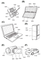
도 15는 전자 기기를 설명하기 위한 도면.1 is a circuit diagram of a level shifter which is an embodiment of the present invention.
2 is an operation timing chart of a level shifter circuit which is an embodiment of the present invention.
3 is a circuit diagram of a level shifter which is an embodiment of the present invention.
4 is a circuit diagram of a level shifter which is an embodiment of the present invention.
5 is a circuit diagram of a level shifter which is an embodiment of the present invention.
6 is a view for explaining an example of a configuration of a transistor which is one embodiment of the present invention.
7 is a view for explaining an example of the configuration of a transistor which is one embodiment of the present invention.
8 is a view for explaining an example of the configuration of a transistor which is one embodiment of the present invention.
9 is a view for explaining an example of a configuration of a transistor which is one embodiment of the present invention.
10 is a cross-sectional schematic diagram of a Cs-corrected high-resolution TEM image and a CAAC-OS in a cross-section of a CAAC-OS.
11 is a Cs-corrected high-resolution TEM image of the plane of CAAC-OS.
12 is a diagram for explaining structural analysis of CAAC-OS and single crystal oxide semiconductor by XRD;
13 is a view showing an electron diffraction pattern of CAAC-OS;
14 is a view showing a change of a crystal part of an In-Ga-Zn oxide by electron irradiation;
15 is a view for explaining an electronic apparatus;
(실시형태 1)(Embodiment 1)
본 발명의 일 형태인 레벨 시프터에 대하여 도 1을 사용하여 설명한다.The level shifter, which is one embodiment of the present invention, will be described with reference to Fig.
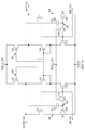
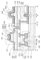
본 발명의 일 형태인 레벨 시프터의 회로도를 도 1에 도시하였다. 본 발명의 일 형태인 레벨 시프터는 제 1 p형 Si-FET(101), 제 2 p형 Si-FET(102), 제 3 p형 Si-FET(103), 제 4 p형 Si-FET(104), 제 1 n형 Si-FET(111), 제 2 n형 Si-FET(112), 제 3 n형 Si-FET(113), 제 4 n형 Si-FET(114), 제 1 OS-FET(121), 제 2 OS-FET(122), 제 3 OS-FET(123), 제 4 OS-FET(124), 제 1 용량 소자(C1)(131), 제 2 용량 소자(C2)(132), 접지 전원선(GND)(141), 저전위 전원선(VDD_L)(142), 고전위 전원선(VDD_H)(143), 입력 신호선(IN)(151), 반전 입력 신호선(INB)(152), 출력 신호선(OUT)(161), 및 반전 출력 신호선(OUTB)(162)으로 구성된다.FIG. 1 shows a circuit diagram of a level shifter which is an embodiment of the present invention. The level shifter, which is one type of the present invention, includes a first p-type Si-FET 101, a second p-type Si-FET 102, a third p-type Si-FET 103, Type Si-FET 104, a first n-type Si-FET 111, a second n-type Si-FET 112, a third n-type Si-FET 113, The first OS-FET 121, the second OS-FET 122, the third OS-FET 123, the fourth OS-FET 124, the first capacitor C1 (131) ) 132, a ground power line (GND) 141, a low potential power line VDD_L 142, a high potential
제 1 p형 Si-FET(101)의 게이트 단자는 제 4 p형 Si-FET(104)의 게이트 단자, 제 4 p형 Si-FET(104)의 소스 단자 및 드레인 단자 중 하나, 및 제 4 n형 Si-FET(114)의 소스 단자 및 드레인 단자 중 하나에 접속되어 있다. 또한, 제 1 p형 Si-FET(101)의 소스 단자 및 드레인 단자 중 하나는 고전위 전원선(VDD_H)(143)에 접속되어 있다. 또한, 제 1 p형 Si-FET(101)의 소스 단자 및 드레인 단자 중 다른 하나는 제 3 p형 Si-FET(103)의 소스 단자 및 드레인 단자 중 하나, 제 1 n형 Si-FET(111)의 소스 단자 및 드레인 단자 중 하나, 제 2 용량 소자(C2)(132)의 단자 중 하나, 및 반전 출력 신호선(OUTB)(162)에 접속되어 있다. 또한, 제 1 p형 Si-FET(101)의 게이트 단자가 접속되어 있는 노드를 N2라고 부를 수 있다.The gate terminal of the first p-type Si-
제 2 p형 Si-FET(102)의 게이트 단자는 제 3 p형 Si-FET(103)의 게이트 단자, 제 3 p형 Si-FET(103)의 소스 단자 및 드레인 단자 중 다른 하나, 및 제 3 n형 Si-FET(113)의 소스 단자 및 드레인 단자 중 하나에 접속되어 있다. 또한, 제 2 p형 Si-FET(102)의 소스 단자 및 드레인 단자 중 하나는 고전위 전원선(VDD_H)(143)에 접속되어 있다. 또한, 제 2 p형 Si-FET(102)의 소스 단자 및 드레인 단자 중 다른 하나는 제 4 p형 Si-FET(104)의 소스 단자 및 드레인 단자 중 다른 하나, 제 2 n형 Si-FET(112)의 소스 단자 및 드레인 단자 중 하나, 제 1 용량 소자(C1)(131)의 단자 중 하나, 및 출력 신호선(OUT)(161)에 접속되어 있다. 또한, 제 2 p형 Si-FET(102)의 게이트 단자가 접속되어 있는 노드를 N1이라고 부를 수 있다.The gate terminal of the second p-type Si-
제 1 n형 Si-FET(111)의 게이트 단자는 입력 신호선(IN)(151), 제 3 n형 Si-FET(113)의 게이트 단자, 및 제 1 OS-FET(121)의 소스 단자 및 드레인 단자 중 하나에 접속되어 있다. 또한, 제 1 n형 Si-FET(111)의 소스 단자 및 드레인 단자 중 다른 하나는 제 3 OS-FET(123)의 소스 단자 및 드레인 단자 중 하나에 접속되어 있다. 또한, 제 1 n형 Si-FET(111)의 소스 단자 및 드레인 단자 중 다른 하나에 접속되어 있는 노드를 N3이라고 부를 수 있다.The gate terminal of the first n-type Si-
제 2 n형 Si-FET(112)의 게이트 단자는 반전 입력 신호선(INB)(152), 제 4 n형 Si-FET(114)의 게이트 단자, 및 제 2 OS-FET(122)의 소스 단자 및 드레인 단자 중 하나에 접속되어 있다. 또한, 제 2 n형 Si-FET(112)의 소스 단자 및 드레인 단자 중 다른 하나는 제 4 OS-FET(124)의 소스 단자 및 드레인 단자 중 하나에 접속되어 있다. 또한, 제 2 n형 Si-FET(112)의 소스 단자 및 드레인 단자 중 다른 하나가 접속되어 있는 노드를 N4라고 부를 수 있다.The gate terminal of the second n-type Si-
제 3 n형 Si-FET(113)의 소스 단자 및 드레인 단자 중 다른 하나는 접지 전원선(GND)(141)에 접속되어 있다.The other of the source terminal and the drain terminal of the third n-type Si-
제 4 n형 Si-FET(114)의 소스 단자 및 드레인 단자 중 다른 하나는 접지 전원선(GND)(141)에 접속되어 있다.The other of the source terminal and the drain terminal of the fourth n-type Si-
제 1 OS-FET(121)의 게이트 단자는 저전위 전원선(VDD_L)(142)에 접속되어 있다. 또한, 제 1 OS-FET(121)의 소스 단자 및 드레인 단자 중 다른 하나는 제 3 OS-FET(123)의 게이트 단자와 제 1 용량 소자(C1)(131)의 단자 중 다른 하나에 접속되어 있다. 또한, 제 1 OS-FET(121)의 소스 단자 및 드레인 단자 중 다른 하나가 접속되어 있는 노드를 N5라고 부를 수 있다.The gate terminal of the first OS-
제 2 OS-FET(122)의 게이트 단자는 저전위 전원선(VDD_L)(142)에 접속되어 있다. 또한, 제 2 OS-FET(122)의 소스 단자 및 드레인 단자 중 다른 하나는 제 4 OS-FET(124)의 게이트 단자와 제 2 용량 소자(C2)(132)의 단자 중 다른 하나에 접속되어 있다. 또한, 제 2 OS-FET(122)의 소스 단자 및 드레인 단자 중 다른 하나가 접속되어 있는 노드를 N6이라고 부를 수 있다.The gate terminal of the second OS-
제 3 OS-FET(123)의 소스 단자 및 드레인 단자 중 다른 하나는 접지 전원선(GND)(141)에 접속되어 있다.The other of the source terminal and the drain terminal of the third OS-
제 4 OS-FET(124)의 소스 단자 및 드레인 단자 중 다른 하나는 접지 전원선(GND)(141)에 접속되어 있다.The other of the source terminal and the drain terminal of the fourth OS-
제 1 p형 Si-FET(101)는 N2의 전위에 따라 고전위 전원선(VDD_H)(143)의 전원 공급을 제어하는 기능을 갖는다.The first p-type Si-
제 2 p형 Si-FET(102)는 N1의 전위에 따라 고전위 전원선(VDD_H)(143)의 전원 공급을 제어하는 기능을 갖는다.The second p-type Si-
제 3 p형 Si-FET(103)는 다이오드 접속되므로 제 1 p형 Si-FET(101)를 통한 고전위 전원선(VDD_H)(143)의 전위 공급을 제한하여 N1의 전위를 완전히 고전위 전원선(VDD_H)(143)의 전위로 상승시키지 않도록 함으로써 제 3 n형 Si-FET(113)를 통한 접지 전원선(GND)(141)의 전위 공급을 용이하게 하는 기능을 갖는다.Since the third p-type Si-
제 4 p형 Si-FET(104)는 다이오드 접속되므로 제 2 p형 Si-FET(102)를 통한 고전위 전원선(VDD_H)(143)의 전위 공급을 제한하여 N2의 전위를 완전히 고전위 전원선(VDD_H)(143)의 전위로 상승시키지 않도록 함으로써 제 4 n형 Si-FET(114)를 통한 접지 전원선(GND)(141)의 전위 공급을 용이하게 하는 기능을 갖는다.Since the fourth p-type Si-
제 1 n형 Si-FET(111)는 제 3 OS-FET(123)보다 빠르게 오프 상태가 됨으로써 관통 전류의 발생을 억제하는 기능을 갖는다.The first n-type Si-
제 2 n형 Si-FET(112)는 제 4 OS-FET(124)보다 빠르게 오프 상태가 됨으로써 관통 전류의 발생을 억제하는 기능을 갖는다.The second n-type Si-
제 3 n형 Si-FET(113)는 N1로의 접지 전원선(GND)(141)의 전원 공급을 제어하는 기능을 갖는다.The third n-type Si-
제 4 n형 Si-FET(114)는 N2로의 접지 전원선(GND)(141)의 전원 공급을 제어하는 기능을 갖는다.The fourth n-type Si-
IN(151)의 전위가 H 전위일 때, 용량 결합에 의하여 N5의 전위가 저전위 전원선(VDD_L)(142)의 전위보다 높은 전위로 상승된 경우, 제 1 OS-FET(121)는 오프 상태가 되어 N5의 상승 전위를 유지하는 기능을 갖는다.When the potential of N5 is raised to a potential higher than the potential of the low potential power supply line (VDD_L) 142 by capacitive coupling when the potential of
INB(152)의 전위가 H 전위일 때, 용량 결합에 의하여 N6의 전위가 저전위 전원선(VDD_L)(142)의 전위보다 높은 전위로 상승된 경우, 제 2 OS-FET(122)는 오프 상태가 되어 N6의 상승 전위를 유지하는 기능을 갖는다.When the potential of N6 is raised to a potential higher than the potential of the low potential power supply line (VDD_L) 142 by capacitive coupling when the potential of the
오프 상태일 때 제 3 OS-FET(123)는 리크 전류를 저감시키는 기능을 갖는다.In the OFF state, the third OS-
오프 상태일 때 제 4 OS-FET(124)는 리크 전류를 저감시키는 기능을 갖는다.The fourth OS-
제 1 용량 소자(C1)(131)는 N5와 OUT(161) 사이에 있고, 용량 결합에 의한 높은 전위를 N5에 공급하여 제 3 OS-FET(123)의 온 전류를 향상시키는 기능을 갖는다. 또한, 용량 결합에 의하여 전위가 충분히 상승된다면, 제 1 용량 소자(C1)(131)를 배선들 사이의 기생 용량 등으로 대체할 수도 있다.The first capacitor C1 (131) is located between N5 and
제 2 용량 소자(C2)(132)는 N6과 OUTB(162) 사이에 있고, 용량 결합에 의한 높은 전위를 N6에 공급하여 제 4 OS-FET(124)의 온 전류를 향상시키는 기능을 갖는다. 또한, 용량 결합에 의하여 전위가 충분히 상승된다면, 제 2 용량 소자(C2)(132)를 배선들 사이의 기생 용량 등으로 대체할 수도 있다.The second capacitor (C2) 132 is located between N6 and
또한, 본 실시형태는 다른 실시형태와 적절히 조합하여 실시할 수 있다.The present embodiment can be implemented in appropriate combination with other embodiments.
(실시형태 2)(Embodiment 2)
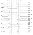
도 2에 도시된 타이밍 차트를 사용하여 도 1의 레벨 시프터의 회로 동작을 설명한다.The circuit operation of the level shifter of FIG. 1 will be described using the timing chart shown in FIG.
초기 상태로서 IN(151)의 전위가 L 전위, INB(152)의 전위가 H 전위를 유지한다고 가정한다. IN(151) 및 INB(152)에 공급되는 신호는 저전위 전원 회로로부터 공급되는 신호이기 때문에, H 전위는 저전위 전원선(VDD_L)(142)의 전위다. 이 때, N1의 전위는 H 전위이지만, 고전위 전원선(VDD_H)(143)의 전위보다 제 3 p형 Si-FET(103)의 문턱 전압만큼 낮은 전위가 N1에 인가된다. 또한, N2의 전위, N5의 전위는 모두 L 전위이고, N6에는 OUTB(162)와의 용량 결합에 의하여, 입력 신호이며 H 전위인 저전위 전원선(VDD_L)(142)의 전위보다 높은 전위가 인가된다.It is assumed that the potential of the
시각 T0에서 IN(151)의 전위가 H 전위가 되면, 제 1 n형 Si-FET(111), 제 3 n형 Si-FET(113), 및 제 3 OS-FET(123)가 온 상태가 되고, INB(152)의 전위가 L 전위가 되면 제 2 n형 Si-FET(112)와 제 4 n형 Si-FET(114)가 오프 상태가 된다. 제 4 OS-FET(124)는 제 2 OS-FET(122)를 통하여 INB(152)의 전위가 공급되고, 게이트 전위가 완전히 L 전위(GND)로 저하될 때까지 온 상태를 유지한다. 또한, 제 4 OS-FET(124)가 어느 정도의 시간 동안 온 상태를 유지하는지는 제 2 OS-FET(122)의 온 전류에 의존한다. IN(151)의 전위가 H 전위가 되어 제 3 n형 Si-FET(113)가 온 상태가 됨으로써 N1의 전위가 저하된다. 이 결과, 제 2 p형 Si-FET(102)를 통하여 고전위 전원선(VDD_H)(143)의 전위가 OUT(161)에 공급되고, OUT(161)의 전위가 상승되기 시작한다. OUT(161)의 전위가 상승되면, 제 4 p형 Si-FET(104)를 통하여 N2에 고전위 전원선(VDD_H)(143)의 전위가 공급된다.The first n-type Si-
또한, IN(151)의 전위가 H 전위가 됨으로써 N5의 전위가 저전위 전원선(VDD_L)(142)의 전위까지 상승된다. 그리고, OUT(161)의 전위가 상승함으로써 제 1 용량 소자(C1)(131)를 통하여 용량 결합이 발생하고, N5의 전위가 저전위 전원선(VDD_L)(142)의 전위보다 높은 전위로 상승된다. 따라서, 제 3 OS-FET(123)의 온 전류가 제 1 n형 Si-FET(111)의 온 전류보다 높게 됨으로써 종래의 레벨 시프터와 같은 정도의 응답 속도로 승압 동작이 가능하다.Further, the potential of
시각 T0 내지 시각 T1 동안은 제 1 p형 Si-FET(101), 제 1 n형 Si-FET(111), 및 제 3 OS-FET(123)를 통하여 고전위 전원선(VDD_H)(143)과 접지 전원선(GND)(141)이 접속된 상태이며, 관통 전류가 발생한다. 이 관통 전류의 양은 제 1 n형 Si-FET(111) 및 제 3 OS-FET(123) 중 온 전류가 작은 쪽의 FET에 의존한다. 또한, 저전위 전원 구동의 n형 Si-FET와 고전위 전원 구동의 p형 Si-FET는 Vgs가 상이하기 때문에 접지 전원선(GND)(141)의 전위를 공급하는 n형 Si-FET의 온 전류와 비교하여 고전위 전원선(VDD_H)(143)의 전위를 공급하는 p형 Si-FET의 온 전류가 크므로 관통 전류 발생시에도 OUTB(162)의 전위는 H 전위를 유지한다. 마찬가지로, 고전위 전원선(VDD_H)(143)의 전위를 공급하는 제 1 p형 Si-FET(101)와 제 3 p형 Si-FET(103)는 접지 전원선(GND)(141)의 전위를 공급하는 제 3 n형 Si-FET(113)보다 온 전류가 크기 때문에 N1의 전위도 H 전위를 유지한다.During the time T0 to time T1, the high potential power line (VDD_H) 143 is connected to the high potential power line (VDD_H) 143 through the first p-type Si-
시각 T1에서 N2의 전위가 고전위 전원선(VDD_H)(143)의 전위보다 제 4 p형 Si-FET(104)의 문턱 전압만큼 낮은 전위까지 상승되면, 제 1 p형 Si-FET(101)가 오프 상태가 된다. OUTB(162)로의 고전위 전원선(VDD_H)(143)으로부터의 전원 공급이 정지되고, 제 1 n형 Si-FET(111)와 제 3 OS-FET(123)를 통하여 접지 전원선(GND)(141)으로부터 전원 공급되어 OUTB(162)의 전위가 저하된다. 또한, OUTB(162)의 전위가 저하되면, 제 2 용량 소자(C2)(132)를 통한 용량 결합에 의하여 N6의 전위가 저하된다. N6의 전위가 접지 전원선(GND)(141)의 전위 즉 L 전위라면 이 상태를 유지한다. N6의 전위가 L 전위가 되면, 제 4 OS-FET(124)가 오프 상태가 된다. OS-FET는 Si-FET와 비교하여 오프 전류가 매우 작기 때문에, 접지 전원선(GND)(141)으로 리크되는 전류량을 저감시킬 수 있고, OUT(161)의 H 전위의 저하를 억제할 수 있다. 또한, N4의 전위는 제 2 n형 Si-FET(112)의 오프 리크 전류에 따라 서서히 상승된다. N4의 전위 상승에 따라 제 2 n형 Si-FET(112)와 제 4 OS-FET(124)의 Vds가 변화되기 때문에 제 2 n형 Si-FET(112)의 오프 전류 값은 트랜지스터의 Vds 특성에 따라 변화된다.At time T1, when the potential of N2 rises to the potential lower than the potential of the high potential power supply line (VDD_H) 143 by the threshold voltage of the fourth p-type Si-
또한, 제 1 p형 Si-FET(101)가 오프 상태가 됨으로써, 제 3 n형 Si-FET(113)를 통하여 접지 전원선(GND)(141)의 전위가 공급되어 OUTB(162)의 전위 변화와 동시에 N1의 전위도 저하된다.When the first p-type Si-
시각 T2에서 OUTB(162), N1, 및 N6의 전위가 L 전위가 됨으로써, 저전위 신호의 승압화가 완료된다.At time T2, the potentials of the
도 1의 회로가 좌우 대칭성을 갖기 때문에, 시각 T3 내지 시각 T5 동안의 동작은 각 소자 또는 노드를 바꾸기만 하면 시각 T0 내지 시각 T2 동안의 동작과 마찬가지이므로 설명을 생략하기로 한다.Since the circuit of Fig. 1 has symmetry, the operation during the time T3 to the time T5 is the same as the operation during the time T0 to the time T2 by simply changing each element or node, and thus the description thereof will be omitted.
상술한 회로 동작에 의하여 제 4 OS-FET(124) 또는 제 3 OS-FET(123)가 온 상태가 될 때 용량 결합에 의하여 게이트 전위를 상승시켜 제 4 OS-FET(124) 또는 제 3 OS-FET(123)의 온 전류를 n형 Si-FET의 온 전류보다 크게 함으로써 OS-FET를 추가하여도 레벨 시프터의 동작을 정상적으로 유지하고 종래의 레벨 시프터와 같은 정도의 응답 속도를 갖는 구성으로 할 수 있다. 또한, OS-FET는 n형 Si-FET보다 오프 전류가 매우 작기 때문에 제 4 OS-FET(124) 또는 제 3 OS-FET(123)가 오프 상태가 됨으로써 OUT(161) 또는 OUTB(162)의 전위가 H 전위를 출력할 때 접지 전원선(GND)(141)으로 리크되는 전류량을 저감시킬 수 있다. 이 결과, 고정 전위 출력 상태인 대기 시의 소비 전력을 저감시킬 수 있다.When the fourth OS-
또한, 본 실시형태는 다른 실시형태와 적절히 조합하여 실시할 수 있다.The present embodiment can be implemented in appropriate combination with other embodiments.
(실시형태 3)(Embodiment 3)
본 발명의 일 형태인 레벨 시프터의 다른 구성에 대하여 도 3을 사용하여 설명한다.Other configurations of the level shifter, which is one form of the present invention, will be described with reference to FIG.
레벨 시프터의 회로도를 도 3에 도시하였다. 본 발명의 일 형태인 레벨 시프터는 제 1 p형 Si-FET(101), 제 2 p형 Si-FET(102), 제 1 n형 Si-FET(111), 제 2 n형 Si-FET(112), 제 5 n형 Si-FET(115), 제 6 n형 Si-FET(116), 제 7 n형 Si-FET(117), 제 8 n형 Si-FET(118), 제 1 OS-FET(121), 제 2 OS-FET(122), 제 3 OS-FET(123), 제 4 OS-FET(124), 제 1 용량 소자(C1)(131), 제 2 용량 소자(C2)(132), 접지 전원선(GND)(141), 저전위 전원선(VDD_L)(142), 고전위 전원선(VDD_H)(143), 입력 신호선(IN)(151), 반전 입력 신호선(INB)(152), 출력 신호선(OUT)(161), 및 반전 출력 신호선(OUTB)(162)으로 구성된다.A circuit diagram of the level shifter is shown in Fig. The level shifter, which is one type of the present invention, includes a first p-type Si-
제 1 p형 Si-FET(101)의 게이트 단자는 제 6 n형 Si-FET(116)의 소스 단자 및 드레인 단자 중 하나와 제 7 n형 Si-FET(117)의 소스 단자 및 드레인 단자 중 하나에 접속되어 있다. 또한, 제 1 p형 Si-FET(101)의 소스 단자 및 드레인 단자 중 하나는 고전위 전원선(VDD_H)(143)에 접속되어 있다. 또한, 제 1 p형 Si-FET(101)의 소스 단자 및 드레인 단자 중 다른 하나는 제 1 n형 Si-FET(111)의 소스 단자 및 드레인 단자 중 하나, 제 8 n형 Si-FET(118)의 소스 단자 및 드레인 단자 중 하나, 제 2 용량 소자(C2)(132)의 단자 중 하나, 및 반전 출력 신호선(OUTB)(162)에 접속되어 있다.The gate terminal of the first p-type Si-
제 2 p형 Si-FET(102)의 게이트 단자는 제 5 n형 Si-FET(115)의 소스 단자 및 드레인 단자 중 하나와 제 8 n형 Si-FET(118)의 소스 단자 및 드레인 단자 중 다른 하나에 접속되어 있다. 제 2 p형 Si-FET(102)의 소스 단자 및 드레인 단자 중 하나는 고전위 전원선(VDD_H)(143)에 접속되어 있다. 제 2 p형 Si-FET(102)의 소스 단자 및 드레인 단자 중 다른 하나는 제 2 n형 Si-FET(112)의 소스 단자 및 드레인 단자 중 하나, 제 7 n형 Si-FET(117)의 소스 단자 및 드레인 단자 중 다른 하나, 제 1 용량 소자(C1)(131)의 단자 중 하나, 및 출력 신호선(OUT)(161)에 접속되어 있다.The gate terminal of the second p-type Si-
제 1 n형 Si-FET(111)의 게이트 단자는 입력 신호선(IN)(151), 제 5 n형 Si-FET(115)의 게이트 단자, 및 제 1 OS-FET(121)의 소스 단자 및 드레인 단자 중 하나에 접속되어 있다. 제 1 n형 Si-FET(111)의 소스 단자 및 드레인 단자 중 다른 하나는 제 3 OS-FET(123)의 소스 단자 및 드레인 단자 중 하나에 접속되어 있다. 또한, 제 1 n형 Si-FET(111)의 소스 단자 및 드레인 단자 중 다른 하나가 접속되어 있는 노드를 N3이라고 부를 수 있다.The gate terminal of the first n-type Si-
제 2 n형 Si-FET(112)의 게이트 단자는 반전 입력 신호선(INB)(152), 제 6 n형 Si-FET(116)의 게이트 단자, 및 제 2 OS-FET(122)의 소스 단자 및 드레인 단자 중 하나에 접속되어 있다. 제 2 n형 Si-FET(112)의 소스 단자 및 드레인 단자 중 다른 하나는 제 4 OS-FET(124)의 소스 단자 및 드레인 단자 중 하나에 접속되어 있다. 또한, 제 2 n형 Si-FET(112)의 소스 단자 및 드레인 단자 중 다른 하나가 접속되어 있는 노드를 N4라고 부를 수 있다.The gate terminal of the second n-type Si-
제 5 n형 Si-FET(115)의 소스 단자 및 드레인 단자 중 다른 하나는 접지 전원선(GND)(141)에 접속되어 있다.The other of the source terminal and the drain terminal of the fifth n-type Si-
제 6 n형 Si-FET(116)의 소스 단자 및 드레인 단자 중 다른 하나는 접지 전원선(GND)(141)에 접속되어 있다.The other of the source terminal and the drain terminal of the sixth n-type Si-
제 7 n형 Si-FET(117)의 게이트 단자는 고전위 전원선(VDD_H)(143)에 접속되어 있다.The gate terminal of the seventh n-type Si-
제 8 n형 Si-FET(118)의 게이트 단자는 고전위 전원선(VDD_H)(143)에 접속되어 있다.The gate terminal of the eighth n-type Si-
제 1 OS-FET(121)의 게이트 단자는 저전위 전원선(VDD_L)(142)에 접속되어 있다. 제 1 OS-FET(121)의 소스 단자 및 드레인 단자 중 다른 하나는 제 3 OS-FET(123)의 게이트 단자와 제 1 용량 소자(C1)(131)의 단자 중 다른 하나에 접속되어 있다. 또한, 제 1 OS-FET(121)의 소스 단자 및 드레인 단자 중 다른 하나가 접속되어 있는 노드를 N5라고 부를 수 있다.The gate terminal of the first OS-
제 2 OS-FET(122)의 게이트 단자는 저전위 전원선(VDD_L)(142)에 접속되어 있다. 제 2 OS-FET(122)의 소스 단자 및 드레인 단자 중 다른 하나는 제 4 OS-FET(124)의 게이트 단자와 제 2 용량 소자(C2)(132)의 단자 중 다른 하나에 접속되어 있다. 또한, 제 2 OS-FET(122)의 소스 단자 및 드레인 단자 중 다른 하나가 접속되어 있는 노드를 N6이라고 부를 수 있다.The gate terminal of the second OS-
제 3 OS-FET(123)의 소스 단자 및 드레인 단자 중 다른 하나는 접지 전원선(GND)(141)에 접속되어 있다.The other of the source terminal and the drain terminal of the third OS-
제 4 OS-FET(124)의 소스 단자 및 드레인 단자 중 다른 하나는 접지 전원선(GND)(141)에 접속되어 있다.The other of the source terminal and the drain terminal of the fourth OS-
제 1 p형 Si-FET(101)는 제 1 p형 Si-FET(101)의 게이트 단자의 전위에 따라 고전위 전원선(VDD_H)(143)의 전원 공급을 제어하는 기능을 갖는다.The first p-type Si-
제 2 p형 Si-FET(102)는 제 2 p형 Si-FET(102)의 게이트 단자의 전위에 따라 고전위 전원선(VDD_H)(143)의 전원 공급을 제어하는 기능을 갖는다.The second p-type Si-
제 1 n형 Si-FET(111)는 제 3 OS-FET(123)보다 빠르게 오프 상태가 됨으로써 관통 전류의 발생을 억제하는 기능을 갖는다.The first n-type Si-
제 2 n형 Si-FET(112)는 제 4 OS-FET(124)보다 빠르게 오프 상태가 됨으로써 관통 전류의 발생을 억제하는 기능을 갖는다.The second n-type Si-
제 5 n형 Si-FET(115)는 제 2 p형 Si-FET(102)의 게이트 단자에 접지 전원선(GND)(141)의 전위를 직접 인가함으로써 레벨 시프터의 전이 동작을 용이하게 하는 기능을 갖는다.The fifth n-type Si-
제 6 n형 Si-FET(116)는 제 1 p형 Si-FET(101)의 게이트 단자에 접지 전원선(GND)(141)의 전위를 직접 인가함으로써 레벨 시프터의 전이 동작을 용이하게 하는 기능을 갖는다.The sixth n-type Si-
제 7 n형 Si-FET(117)는 소스 단자 또는 드레인 단자의 전위에 따라 저항이 변화되는 가변 저항으로서 기능하고, 레벨 시프터의 전이 동작을 용이하게 하는 기능을 갖는다.The seventh n-type Si-
제 8 n형 Si-FET(118)는 소스 단자 또는 드레인 단자의 전위에 따라 저항이 변화되는 가변 저항으로서 기능하고, 레벨 시프터의 전이 동작을 용이하게 하는 기능을 갖는다.The eighth n-type Si-
입력 신호선(IN)(151)의 전위가 H 전위일 때, 용량 결합에 의하여 N5의 전위가 저전위 전원선(VDD_L)(142)의 전위보다 높은 전위로 상승된 경우, 제 1 OS-FET(121)는 오프 상태가 되어 N5의 상승 전위를 유지하는 기능을 갖는다.When the potential of N5 is raised to a potential higher than the potential of the low potential power supply line (VDD_L) 142 by capacitive coupling when the potential of the input signal line (IN) 151 is H potential, 121 are turned off to maintain the rising potential of N5.
반전 입력 신호선(INB)(152)의 전위가 H 전위일 때, 용량 결합에 의하여 N6의 전위가 저전위 전원선(VDD_L)(142)의 전위보다 높은 전위로 상승된 경우, 제 2 OS-FET(122)는 오프 상태가 되어 N6의 상승 전위를 유지하는 기능을 갖는다.When the potential of the N6 is raised to a potential higher than the potential of the low potential power supply line (VDD_L) 142 by capacitive coupling when the potential of the inverting input signal line (INB) 152 is H potential, (122) is in the off state and has the function of maintaining the rising potential of N6.
오프 상태일 때 제 3 OS-FET(123)는 리크 전류를 저감시키는 기능을 갖는다.In the OFF state, the third OS-
오프 상태일 때 제 4 OS-FET(124)는 리크 전류를 저감시키는 기능을 갖는다.The fourth OS-
제 1 용량 소자(C1)(131)는 N5와 출력 신호선(OUT)(161) 사이에 있고, 용량 결합에 의한 높은 전위를 N5에 공급하여 제 3 OS-FET(123)의 온 전류를 향상시키는 기능을 갖는다. 또한, 용량 결합에 의하여 전위가 충분히 상승된다면, 제 1 용량 소자(C1)(131)를 배선들 사이의 기생 용량 등으로 대체할 수도 있다.The first capacitor C1 (131) is between N5 and the output signal line (OUT) 161 and supplies a high potential by capacitive coupling to N5 to improve the on current of the third OS-
제 2 용량 소자(C2)(132)는 N6과 반전 출력 신호선(OUTB)(162) 사이에 있고, 용량 결합에 의한 높은 전위를 N6에 공급하여 제 4 OS-FET(124)의 온 전류를 향상시키는 기능을 갖는다. 또한, 용량 결합에 의하여 전위가 충분히 상승된다면, 제 2 용량 소자(C2)(132)를 배선들 사이의 기생 용량 등으로 대체할 수도 있다.The second capacitor (C2) 132 is between N6 and the inverted output signal line (OUTB) 162 and supplies a high potential by capacitive coupling to N6 to improve the on current of the fourth OS-
또한, 본 실시형태는 다른 실시형태와 적절히 조합하여 실시할 수 있다.The present embodiment can be implemented in appropriate combination with other embodiments.
(실시형태 4)(Fourth Embodiment)
본 발명의 일 형태인 레벨 시프터의 다른 구성에 대하여 도 4를 사용하여 설명한다.Other configurations of the level shifter, which is one form of the present invention, will be described with reference to FIG.
레벨 시프터의 회로도를 도 4에 도시하였다. 본 발명의 일 형태인 레벨 시프터는 제 1 p형 Si-FET(101), 제 2 p형 Si-FET(102), 제 1 n형 Si-FET(111), 제 2 n형 Si-FET(112), 제 5 n형 Si-FET(115), 제 6 n형 Si-FET(116), 제 1 OS-FET(121), 제 2 OS-FET(122), 제 3 OS-FET(123), 제 4 OS-FET(124), 제 1 용량 소자(C1)(131), 제 2 용량 소자(C2)(132), 제 1 저항 소자(171), 제 2 저항 소자(172), 접지 전원선(GND)(141), 저전위 전원선(VDD_L)(142), 고전위 전원선(VDD_H)(143), 입력 신호선(IN)(151), 반전 입력 신호선(INB)(152), 출력 신호선(OUT)(161), 및 반전 출력 신호선(OUTB)(162)으로 구성된다.A circuit diagram of the level shifter is shown in Fig. The level shifter, which is one type of the present invention, includes a first p-type Si-
제 1 p형 Si-FET(101)의 게이트 단자는 제 6 n형 Si-FET(116)의 소스 단자 및 드레인 단자 중 하나와 제 1 저항 소자(171)의 단자 중 하나에 접속되어 있다. 또한, 제 1 p형 Si-FET(101)의 소스 단자 및 드레인 단자 중 하나는 고전위 전원선(VDD_H)(143)에 접속되어 있다. 또한, 제 1 p형 Si-FET(101)의 소스 단자 및 드레인 단자 중 다른 하나는 제 1 n형 Si-FET(111)의 소스 단자 및 드레인 단자 중 하나, 제 2 저항 소자(172)의 단자 중 하나, 제 2 용량 소자(C2)(132)의 단자 중 하나, 및 반전 출력 신호선(OUTB)(162)에 접속되어 있다.The gate terminal of the first p-type Si-
제 2 p형 Si-FET(102)의 게이트 단자는 제 5 n형 Si-FET(115)의 소스 단자 및 드레인 단자 중 하나와 제 2 저항 소자(172)의 단자 중 다른 하나에 접속되어 있다. 또한, 제 2 p형 Si-FET(102)의 소스 단자 및 드레인 단자 중 하나는 고전위 전원선(VDD_H)(143)에 접속되어 있다. 또한, 제 2 p형 Si-FET(102)의 소스 단자 및 드레인 단자 중 다른 하나는 제 2 n형 Si-FET(112)의 소스 단자 및 드레인 단자 중 하나, 제 1 저항 소자(171)의 단자 중 다른 하나, 제 1 용량 소자(C1)(131)의 단자 중 하나, 및 출력 신호선(OUT)(161)에 접속되어 있다.The gate terminal of the second p-type Si-
제 1 n형 Si-FET(111)의 게이트 단자는 입력 신호선(IN)(151), 제 1 OS-FET(121)의 소스 단자 및 드레인 단자 중 하나, 및 제 5 n형 Si-FET(115)의 게이트 단자에 접속되어 있다. 또한, 제 1 n형 Si-FET(111)의 소스 단자 및 드레인 단자 중 다른 하나는 제 3 OS-FET(123)의 소스 단자 및 드레인 단자 중 하나에 접속되어 있다. 또한, 제 1 n형 Si-FET(111)의 소스 단자 및 드레인 단자 중 다른 하나에 접속되어 있는 노드를 N3이라고 부를 수 있다.The gate terminal of the first n-type Si-
제 2 n형 Si-FET(112)의 게이트 단자는 반전 입력 신호선(INB)(152), 제 2 OS-FET(122)의 소스 단자 및 드레인 단자 중 하나, 및 제 6 n형 Si-FET(116)의 게이트 단자에 접속되어 있다. 또한, 제 2 n형 Si-FET(112)의 소스 단자 및 드레인 단자 중 다른 하나는 제 4 OS-FET(124)의 소스 단자 및 드레인 단자 중 하나에 접속되어 있다. 또한, 제 2 n형 Si-FET(112)의 소스 단자 및 드레인 단자 중 다른 하나에 접속되어 있는 노드를 N4라고 부를 수 있다.The gate terminal of the second n-type Si-
제 5 n형 Si-FET(115)의 소스 단자 및 드레인 단자 중 다른 하나는 접지 전원선(GND)(141)에 접속되어 있다.The other of the source terminal and the drain terminal of the fifth n-type Si-
제 6 n형 Si-FET(116)의 소스 단자 및 드레인 단자 중 다른 하나는 접지 전원선(GND)(141)에 접속되어 있다.The other of the source terminal and the drain terminal of the sixth n-type Si-
제 1 OS-FET(121)의 게이트 단자는 저전위 전원선(VDD_L)(142)에 접속되어 있다. 또한, 제 1 OS-FET(121)의 소스 단자 및 드레인 단자 중 다른 하나는 제 3 OS-FET(123)의 게이트 단자와 제 1 용량 소자(C1)(131)의 단자 중 다른 하나에 접속되어 있다. 또한, 제 1 OS-FET(121)의 소스 단자 및 드레인 단자 중 다른 하나가 접속되어 있는 노드를 N5라고 부를 수 있다.The gate terminal of the first OS-
제 2 OS-FET(122)의 게이트 단자는 저전위 전원선(VDD_L)(142)에 접속되어 있다. 또한, 제 2 OS-FET(122)의 소스 단자 및 드레인 단자 중 다른 하나는 제 4 OS-FET(124)의 게이트 단자와 제 2 용량 소자(C2)(132)의 단자 중 다른 하나에 접속되어 있다. 또한, 제 2 OS-FET(122)의 소스 단자 및 드레인 단자 중 다른 하나가 접속되어 있는 노드를 N6이라고 부를 수 있다.The gate terminal of the second OS-
제 3 OS-FET(123)의 소스 단자 및 드레인 단자 중 다른 하나는 접지 전원선(GND)(141)에 접속되어 있다.The other of the source terminal and the drain terminal of the third OS-
제 4 OS-FET(124)의 소스 단자 및 드레인 단자 중 다른 하나는 접지 전원선(GND)(141)에 접속되어 있다.The other of the source terminal and the drain terminal of the fourth OS-
제 1 저항 소자(171)의 단자 중 다른 하나는 출력 신호선(OUT)(161)에 접속되어 있다.And the other of the terminals of the
제 2 저항 소자(172)의 단자 중 하나는 반전 출력 신호선(OUTB)(162)에 접속되어 있다.One of the terminals of the second
제 1 p형 Si-FET(101)는 제 1 p형 Si-FET(101)의 게이트 단자의 전위에 따라 고전위 전원선(VDD_H)(143)의 전원 공급을 제어하는 기능을 갖는다.The first p-type Si-
제 2 p형 Si-FET(102)는 제 2 p형 Si-FET(102)의 게이트 단자의 전위에 따라 고전위 전원선(VDD_H)(143)의 전원 공급을 제어하는 기능을 갖는다.The second p-type Si-
제 1 n형 Si-FET(111)는 제 3 OS-FET(123)보다 빠르게 오프 상태가 됨으로써 관통 전류의 발생을 억제하는 기능을 갖는다.The first n-type Si-
제 2 n형 Si-FET(112)는 제 4 OS-FET(124)보다 빠르게 오프 상태가 됨으로써 관통 전류의 발생을 억제하는 기능을 갖는다.The second n-type Si-
제 5 n형 Si-FET(115)는 제 2 p형 Si-FET(102)의 게이트 단자에 접지 전원선(GND)(141)의 전위를 직접 인가함으로써 레벨 시프터의 전이 동작을 용이하게 하는 기능을 갖는다.The fifth n-type Si-
제 6 n형 Si-FET(116)는 제 1 p형 Si-FET(101)의 게이트 단자에 접지 전원선(GND)(141)의 전위를 직접 인가함으로써 레벨 시프터의 전이 동작을 용이하게 하는 기능을 갖는다.The sixth n-type Si-
입력 신호선(IN)(151)의 전위가 H 전위일 때, 용량 결합에 의하여 N5의 전위가 저전위 전원선(VDD_L)(142)의 전위보다 높은 전위로 상승된 경우, 제 1 OS-FET(121)는 오프 상태가 되어 N5의 상승 전위를 유지하는 기능을 갖는다.When the potential of N5 is raised to a potential higher than the potential of the low potential power supply line (VDD_L) 142 by capacitive coupling when the potential of the input signal line (IN) 151 is H potential, 121 are turned off to maintain the rising potential of N5.
반전 입력 신호선(INB)(152)의 전위가 H 전위일 때, 용량 결합에 의하여 N6의 전위가 저전위 전원선(VDD_L)(142)의 전위보다 높은 전위로 상승된 경우, 제 2 OS-FET(122)는 오프 상태가 되어 N6의 상승 전위를 유지하는 기능을 갖는다.When the potential of the N6 is raised to a potential higher than the potential of the low potential power supply line (VDD_L) 142 by capacitive coupling when the potential of the inverting input signal line (INB) 152 is H potential, (122) is in the off state and has the function of maintaining the rising potential of N6.
오프 상태일 때 제 3 OS-FET(123)는 리크 전류를 저감시키는 기능을 갖는다.In the OFF state, the third OS-
오프 상태일 때 제 4 OS-FET(124)는 리크 전류를 저감시키는 기능을 갖는다.The fourth OS-
제 1 용량 소자(C1)(131)는 N5와 출력 신호선(OUT)(161) 사이에 있고, 용량 결합에 의한 높은 전위를 N5에 공급하여 제 3 OS-FET(123)의 온 전류를 향상시키는 기능을 갖는다. 또한, 용량 결합에 의하여 전위가 충분히 상승된다면, 제 1 용량 소자(C1)(131)를 배선들 사이의 기생 용량 등으로 대체할 수도 있다.The first capacitor C1 (131) is between N5 and the output signal line (OUT) 161 and supplies a high potential by capacitive coupling to N5 to improve the on current of the third OS-
제 2 용량 소자(C2)(132)는 N6과 반전 출력 신호선(OUTB)(162) 사이에 있고, 용량 결합에 의한 높은 전위를 N6에 공급하여 제 4 OS-FET(124)의 온 전류를 향상시키는 기능을 갖는다. 또한, 용량 결합에 의하여 전위가 충분히 상승된다면, 제 2 용량 소자(C2)(132)를 배선들 사이의 기생 용량 등으로 대체할 수도 있다.The second capacitor (C2) 132 is between N6 and the inverted output signal line (OUTB) 162 and supplies a high potential by capacitive coupling to N6 to improve the on current of the fourth OS-
제 1 저항 소자(171)는 제 1 p형 Si-FET(101)를 통한 고전위 전원선(VDD_H)(143)의 전위 공급을 제한하는 저항으로서의 기능을 갖는다. 이로써, 제 6 n형 Si-FET(116)를 통한 접지 전원선(GND)(141)의 전위 공급을 용이하게 하여 레벨 시프터의 전이 동작을 용이하게 하는 기능을 갖는다.The first
제 2 저항 소자(172)는 제 2 p형 Si-FET(102)를 통한 고전위 전원선(VDD_H)(143)의 전위 공급을 제한하는 저항으로서의 기능을 갖는다. 이로써, 제 5 n형 Si-FET(115)를 통한 접지 전원선(GND)(141)의 전위 공급을 용이하게 하여 레벨 시프터의 전이 동작을 용이하게 하는 기능을 갖는다.The second
또한, 본 실시형태는 다른 실시형태와 적절히 조합하여 실시할 수 있다.The present embodiment can be implemented in appropriate combination with other embodiments.
(실시형태 5)(Embodiment 5)
본 발명의 일 형태인 레벨 시프터의 다른 구성예에 대하여 도 5를 사용하여 설명한다.Another configuration example of the level shifter which is one form of the present invention will be described with reference to Fig.
레벨 시프터의 회로도를 도 5에 도시하였다. 본 발명의 일 형태인 레벨 시프터는 제 1 p형 Si-FET(101), 제 2 p형 Si-FET(102), 제 3 p형 Si-FET(103), 제 4 p형 Si-FET(104), 제 1 n형 Si-FET(111), 제 2 n형 Si-FET(112), 제 3 n형 Si-FET(113), 제 4 n형 Si-FET(114), 제 5 n형 Si-FET(115), 제 6 n형 Si-FET(116), 제 7 n형 Si-FET(117), 제 8 n형 Si-FET(118), 제 1 OS-FET(121), 제 2 OS-FET(122), 제 3 OS-FET(123), 제 4 OS-FET(124), 제 1 용량 소자(C1)(131), 제 2 용량 소자(C2)(132), 접지 전원선(GND)(141), 저전위 전원선(VDD_L)(142), 고전위 전원선(VDD_H)(143), 입력 신호선(IN)(151), 반전 입력 신호선(INB)(152), 출력 신호선(OUT)(161), 및 반전 출력 신호선(OUTB)(162)으로 구성된다.A circuit diagram of the level shifter is shown in Fig. The level shifter, which is one type of the present invention, includes a first p-type Si-
제 1 p형 Si-FET(101)의 게이트 단자는 제 6 n형 Si-FET(116)의 소스 단자 및 드레인 단자 중 하나와 제 7 n형 Si-FET(117)의 소스 단자 및 드레인 단자 중 하나에 접속되어 있다. 또한, 제 1 p형 Si-FET(101)의 소스 단자 및 드레인 단자 중 하나는 고전위 전원선(VDD_H)(143)에 접속되어 있다. 또한, 제 1 p형 Si-FET(101)의 소스 단자 및 드레인 단자 중 다른 하나는 제 3 p형 Si-FET(103)의 소스 단자 및 드레인 단자 중 하나, 제 1 n형 Si-FET(111)의 소스 단자 및 드레인 단자 중 하나, 제 2 용량 소자(C2)(132)의 단자 중 하나, 및 반전 출력 신호선(OUTB)(162)에 접속되어 있다.The gate terminal of the first p-type Si-
제 2 p형 Si-FET(102)의 게이트 단자는 제 5 n형 Si-FET(115)의 소스 단자 및 드레인 단자 중 하나와 제 8 n형 Si-FET(118)의 소스 단자 및 드레인 단자 중 하나에 접속되어 있다. 또한, 제 2 p형 Si-FET(102)의 소스 단자 및 드레인 단자 중 하나는 고전위 전원선(VDD_H)(143)에 접속되어 있다. 또한, 제 2 p형 Si-FET(102)의 소스 단자 및 드레인 단자 중 다른 하나는 제 4 p형 Si-FET(104)의 소스 단자 및 드레인 단자 중 하나, 제 2 n형 Si-FET(112)의 소스 단자 및 드레인 단자 중 하나, 제 1 용량 소자(C1)(131)의 단자 중 하나, 및 출력 신호선(OUT)(161)에 접속되어 있다.The gate terminal of the second p-type Si-
제 3 p형 Si-FET(103)의 게이트 단자는 제 3 p형 Si-FET(103)의 소스 단자 및 드레인 단자 중 다른 하나,제 3 n형 Si-FET(113)의 소스 단자 및 드레인 단자 중 하나, 및 제 8 n형 Si-FET(118)의 소스 단자 및 드레인 단자 중 다른 하나에 접속되어 있다.The gate terminal of the third p-type Si-
제 4 p형 Si-FET(104)의 게이트 단자는 제 4 p형 Si-FET(104)의 소스 단자 및 드레인 단자 중 다른 하나,제 4 n형 Si-FET(114)의 소스 단자 및 드레인 단자 중 하나, 및 제 7 n형 Si-FET(117)의 소스 단자 및 드레인 단자 중 다른 하나에 접속되어 있다.The gate terminal of the fourth p-type Si-
제 1 n형 Si-FET(111)의 게이트 단자는 입력 신호선(IN)(151), 제 3 n형 Si-FET(113)의 게이트 단자, 제 5 n형 Si-FET(115)의 게이트 단자, 및 제 1 OS-FET(121)의 소스 단자 및 드레인 단자 중 하나에 접속되어 있다. 또한, 제 1 n형 Si-FET(111)의 소스 단자 및 드레인 단자 중 다른 하나는 제 3 OS-FET(123)의 소스 단자 및 드레인 단자 중 하나에 접속되어 있다. 또한, 제 1 n형 Si-FET(111)의 소스 단자 및 드레인 단자 중 다른 하나가 접속되어 있는 노드를 N3이라고 부를 수 있다.The gate terminal of the first n-type Si-
제 2 n형 Si-FET(112)의 게이트 단자는 반전 입력 신호선(INB)(152), 제 4 n형 Si-FET(114)의 게이트 단자, 제 6 n형 Si-FET(116)의 게이트 단자, 및 제 2 OS-FET(122)의 소스 단자 및 드레인 단자 중 하나에 접속되어 있다. 또한, 제 2 n형 Si-FET(112)의 소스 단자 및 드레인 단자 중 다른 하나는 제 4 OS-FET(124)의 소스 단자 및 드레인 단자 중 하나에 접속되어 있다. 또한, 제 2 n형 Si-FET(112)의 소스 단자 및 드레인 단자 중 다른 하나에 접속되어 있는 노드를 N4라고 부를 수 있다.The gate terminal of the second n-type Si-
제 3 n형 Si-FET(113)의 소스 단자 및 드레인 단자 중 다른 하나는 접지 전원선(GND)(141)에 접속되어 있다.The other of the source terminal and the drain terminal of the third n-type Si-
제 4 n형 Si-FET(114)의 소스 단자 및 드레인 단자 중 다른 하나는 접지 전원선(GND)(141)에 접속되어 있다.The other of the source terminal and the drain terminal of the fourth n-type Si-
제 5 n형 Si-FET(115)의 소스 단자 및 드레인 단자 중 다른 하나는 접지 전원선(GND)(141)에 접속되어 있다.The other of the source terminal and the drain terminal of the fifth n-type Si-
제 6 n형 Si-FET(116)의 소스 단자 및 드레인 단자 중 다른 하나는 접지 전원선(GND)(141)에 접속되어 있다.The other of the source terminal and the drain terminal of the sixth n-type Si-
제 7 n형 Si-FET(117)의 게이트 단자는 고전위 전원선(VDD_H)(143)에 접속되어 있다.The gate terminal of the seventh n-type Si-
제 8 n형 Si-FET(118)의 게이트 단자는 고전위 전원선(VDD_H)(143)에 접속되어 있다.The gate terminal of the eighth n-type Si-
제 1 OS-FET(121)의 게이트 단자는 저전위 전원선(VDD_L)(142)에 접속되어 있다. 또한, 제 1 OS-FET(121)의 소스 단자 및 드레인 단자 중 다른 하나는 제 3 OS-FET(123)의 게이트 단자와 제 1 용량 소자(C1)(131)의 단자 중 다른 하나에 접속되어 있다. 또한, 제 1 OS-FET(121)의 소스 단자 및 드레인 단자 중 다른 하나가 접속되어 있는 노드를 N5라고 부를 수 있다.The gate terminal of the first OS-
제 2 OS-FET(122)의 게이트 단자는 저전위 전원선(VDD_L)(142)에 접속되어 있다. 또한, 제 2 OS-FET(122)의 소스 단자 및 드레인 단자 중 다른 하나는 제 4 OS-FET(124)의 게이트 단자와 제 2 용량 소자(C2)(132)의 단자 중 다른 하나에 접속되어 있다. 또한, 제 2 OS-FET(122)의 소스 단자 및 드레인 단자 중 다른 하나가 접속되어 있는 노드를 N6이라고 부를 수 있다.The gate terminal of the second OS-
제 3 OS-FET(123)의 소스 단자 및 드레인 단자 중 다른 하나는 접지 전원선(GND)(141)에 접속되어 있다.The other of the source terminal and the drain terminal of the third OS-
제 4 OS-FET(124)의 소스 단자 및 드레인 단자 중 다른 하나는 접지 전원선(GND)(141)에 접속되어 있다.The other of the source terminal and the drain terminal of the fourth OS-
제 1 p형 Si-FET(101)는 제 1 p형 Si-FET(101)의 게이트 단자의 전위에 따라 고전위 전원선(VDD_H)(143)의 전원 공급을 제어하는 기능을 갖는다.The first p-type Si-
제 2 p형 Si-FET(102)는 제 2 p형 Si-FET(102)의 게이트 단자의 전위에 따라 고전위 전원선(VDD_H)(143)의 전원 공급을 제어하는 기능을 갖는다.The second p-type Si-
제 3 p형 Si-FET(103)는 다이오드 접속되므로 제 1 p형 Si-FET(101)를 통한 고전위 전원선(VDD_H)(143)의 전위 공급을 제한하여 게이트 단자의 전위를 완전히 고전위 전원선(VDD_H)(143)의 전위로 상승시키지 않도록 함으로써 제 3 n형 Si-FET(113)를 통한 접지 전원선(GND)(141)의 전위 공급을 용이하게 하는 기능을 갖는다.Since the third p-type Si-
제 4 p형 Si-FET(104)는 다이오드 접속되므로 제 2 p형 Si-FET(102)를 통한 고전위 전원선(VDD_H)(143)의 전위 공급을 제한하여 게이트 단자의 전위를 완전히 고전위 전원선(VDD_H)(143)의 전위로 상승시키지 않도록 함으로써 제 4 n형 Si-FET(114)를 통한 접지 전원선(GND)(141)의 전위 공급을 용이하게 하는 기능을 갖는다.Since the fourth p-type Si-
제 1 n형 Si-FET(111)는 제 3 OS-FET(123)보다 빠르게 오프 상태가 됨으로써 관통 전류의 발생을 저감시키는 기능을 갖는다.The first n-type Si-
제 2 n형 Si-FET(112)는 제 4 OS-FET(124)보다 빠르게 오프 상태가 됨으로써 관통 전류의 발생을 저감시키는 기능을 갖는다.The second n-type Si-
제 3 n형 Si-FET(113)는 제 3 p형 Si-FET(103)의 게이트 단자로의 접지 전원선(GND)(141)의 전원 공급을 제어하는 기능을 갖는다.The third n-type Si-
제 4 n형 Si-FET(114)는 제 4 p형 Si-FET(104)의 게이트 단자로의 접지 전원선(GND)(141)의 전원 공급을 제어하는 기능을 갖는다.The fourth n-type Si-
제 5 n형 Si-FET(115)는 제 2 p형 Si-FET(102)의 게이트 단자에 접지 전원선(GND)(141)의 전위를 직접 인가함으로써 레벨 시프터의 전이 동작을 용이하게 하는 기능을 갖는다.The fifth n-type Si-
제 6 n형 Si-FET(116)는 제 1 p형 Si-FET(101)의 게이트 단자에 접지 전원선(GND)(141)의 전위를 직접 인가함으로써 레벨 시프터의 전이 동작을 용이하게 하는 기능을 갖는다.The sixth n-type Si-
제 7 n형 Si-FET(117)는 소스 단자 또는 드레인 단자의 전위에 따라 저항이 변화되는 가변 저항으로서 기능하고, 레벨 시프터의 전이 동작을 용이하게 하는 기능을 갖는다.The seventh n-type Si-
제 8 n형 Si-FET(118)는 소스 단자 또는 드레인 단자의 전위에 따라 저항이 변화되는 가변 저항으로서 기능하고, 레벨 시프터의 전이 동작을 용이하게 하는 기능을 갖는다.The eighth n-type Si-
입력 신호선(IN)(151)의 전위가 H 전위일 때, 용량 결합에 의하여 N5의 전위가 저전위 전원선(VDD_L)(142)의 전위보다 높은 전위로 상승된 경우, 제 1 OS-FET(121)는 오프 상태가 되어 N5의 상승 전위를 유지하는 기능을 갖는다.When the potential of N5 is raised to a potential higher than the potential of the low potential power supply line (VDD_L) 142 by capacitive coupling when the potential of the input signal line (IN) 151 is H potential, 121 are turned off to maintain the rising potential of N5.
반전 입력 신호선(INB)(152)의 전위가 H 전위일 때, 용량 결합에 의하여 N6의 전위가 저전위 전원선(VDD_L)(142)의 전위보다 높은 전위로 상승된 경우, 제 2 OS-FET(122)는 오프 상태가 되어 N6의 상승 전위를 유지하는 기능을 갖는다.When the potential of the N6 is raised to a potential higher than the potential of the low potential power supply line (VDD_L) 142 by capacitive coupling when the potential of the inverting input signal line (INB) 152 is H potential, (122) is in the off state and has the function of maintaining the rising potential of N6.
오프 상태일 때 제 3 OS-FET(123)는 리크 전류를 저감시키는 기능을 갖는다.In the OFF state, the third OS-
오프 상태일 때 제 4 OS-FET(124)는 리크 전류를 저감시키는 기능을 갖는다.The fourth OS-
제 1 용량 소자(C1)(131)는 N5와 출력 신호선(OUT)(161) 사이에 있고, 용량 결합에 의한 높은 전위를 N5에 공급하여 제 3 OS-FET(123)의 온 전류를 향상시키는 기능을 갖는다. 또한, 용량 결합에 의하여 전위가 충분히 상승된다면, 제 1 용량 소자(C1)(131)를 배선들 사이의 기생 용량 등으로 대체할 수도 있다.The first capacitor C1 (131) is between N5 and the output signal line (OUT) 161 and supplies a high potential by capacitive coupling to N5 to improve the on current of the third OS-
제 2 용량 소자(C2)(132)는 N6과 반전 출력 신호선(OUTB)(162) 사이에 있고, 용량 결합에 의한 높은 전위를 N6에 공급하여 제 4 OS-FET(124)의 온 전류를 향상시키는 기능을 갖는다. 또한, 용량 결합에 의하여 전위가 충분히 상승된다면, 제 2 용량 소자(C2)(132)를 배선들 사이의 기생 용량 등으로 대체할 수도 있다.The second capacitor (C2) 132 is between N6 and the inverted output signal line (OUTB) 162 and supplies a high potential by capacitive coupling to N6 to improve the on current of the fourth OS-
또한, 본 실시형태는 다른 실시형태와 적절히 조합하여 실시할 수 있다.The present embodiment can be implemented in appropriate combination with other embodiments.
(실시형태 6)(Embodiment 6)
본 실시형태에서는 본 발명의 일 형태인 레벨 시프터 회로에 사용할 수 있는 트랜지스터의 구성예에 대하여 설명한다.In the present embodiment, a configuration example of a transistor that can be used in a level shifter circuit which is one form of the present invention will be described.
<트랜지스터의 구조에 대하여>≪ Structure of Transistor >
트랜지스터의 단면 구조를 도 6에 도시하였다. 도 6은 단결정 실리콘 기판에 채널 형성 영역을 갖는 트랜지스터(아래에서 Si 트랜지스터라고도 기재함)(1102) 위에 산화물 반도체막에 채널 형성 영역을 갖는 트랜지스터(아래에서 OS 트랜지스터라고도 기재함)(1101)가 형성된 경우를 도시한 것이다. 예를 들어 트랜지스터(1101)로서 OS-FET(121)를 사용할 수 있고, 트랜지스터(1102)로서 n형 Si-FET(113)를 사용할 수 있다.The cross-sectional structure of the transistor is shown in Fig. 6 shows a state in which a transistor 1101 (also referred to as an OS transistor) 1101 having a channel formation region in an oxide semiconductor film is formed on a transistor (also referred to as Si transistor hereinafter) 1102 having a channel formation region in a single crystal silicon substrate FIG. For example, the OS-
트랜지스터(1102)는 비정질, 미결정, 다결정, 또는 단결정인, 실리콘 또는 저마늄 등으로 이루어진 반도체막 또는 반도체 기판에 채널 형성 영역을 가져도 좋다. 또는, 트랜지스터(1102)는 산화물 반도체막 또는 산화물 반도체 기판에 채널 형성 영역을 가져도 좋다. 모든 트랜지스터가 산화물 반도체막 또는 산화물 반도체 기판에 채널 형성 영역을 갖는 경우에는, 트랜지스터(1102) 위에 트랜지스터(1101)를 적층시키지 않아도 되고, 트랜지스터(1101) 및 트랜지스터(1102)를 동일 층에 형성하여도 좋다.The
실리콘 박막을 사용하여 트랜지스터(1102)를 형성하는 경우, 이 박막에는 플라즈마 CVD법 등의 기상 성장법 또는 스퍼터링법으로 제작된 비정질 실리콘, 레이저 조사 등의 처리에 의하여 비정질 실리콘을 결정화시킨 다결정 실리콘, 단결정 실리콘 웨이퍼에 수소 이온 등을 주입하여 표층부를 박리한 단결정 실리콘 등을 사용할 수 있다.In the case of forming the
트랜지스터(1102)가 형성되는 반도체 기판(801)으로서는 예를 들어 실리콘 기판, 저마늄 기판, 실리콘 저마늄 기판 등을 사용할 수 있다. 도 6은 반도체 기판(801)으로서 단결정 실리콘 기판을 사용한 경우를 도시한 것이다.As the
또한, 트랜지스터(1102)는 소자 분리법에 의하여 전기적으로 분리되어 있다. 소자 분리법으로서는 선택 산화법(LOCOS법: Local Oxidation of Silicon법), 트렌치 분리법(STI법: Shallow Trench Isolation법) 등을 사용할 수 있다. 도 6은 트렌치 분리법에 의하여 트랜지스터(1102)를 전기적으로 분리한 경우를 예시한 것이다. 구체적으로 말하면, 도 6은 에칭 처리 등에 의하여 반도체 기판(801)에 트렌치를 형성한 후 이 트렌치에 산화실리콘 등이 포함된 절연물을 매립함으로써 형성되는 소자 분리 영역(810)에 의하여 트랜지스터(1102)를 소자 분리시킨 경우를 도시한 것이다.Further, the
트랜지스터(1102) 위에는 절연막(811)이 제공되어 있다. 절연막(811)에는 개구부가 형성되어 있다. 그리고, 이 개구부에는 트랜지스터(1102)의 소스 및 드레인 각각에 전기적으로 접속되어 있는 도전막(825) 및 도전막(826)과, 트랜지스터(1102)의 게이트에 전기적으로 접속되어 있는 도전막(827)이 형성되어 있다.On the
그리고, 도전막(825)은 절연막(811) 위에 형성된 도전막(834)에 전기적으로 접속되어 있고, 도전막(826)은 절연막(811) 위에 형성된 도전막(835)에 전기적으로 접속되어 있고, 도전막(827)은 절연막(811) 위에 형성된 도전막(836)에 전기적으로 접속되어 있다.The
도전막(834) 내지 도전막(836) 위에는 절연막(812)이 제공되어 있다. 절연막(812)에는 개구부가 형성되어 있고, 이 개구부에 도전막(836)에 전기적으로 접속되어 있는 도전막(837)이 형성되어 있다. 그리고, 도전막(837)은 절연막(812) 위에 형성된 도전막(851)에 전기적으로 접속되어 있다.An insulating
또한, 도전막(851) 위에는 절연막(813)이 형성되어 있다. 절연막(813)에는 개구부가 형성되어 있고, 이 개구부에 도전막(851)에 전기적으로 접속되어 있는 도전막(852)이 형성되어 있다. 그리고, 도전막(852)은 절연막(813) 위에 형성된 도전막(853)에 전기적으로 접속되어 있다. 또한, 절연막(813) 위에는 도전막(844)이 형성되어 있다.An insulating
도전막(853) 및 도전막(844) 위에는 절연막(861)이 형성되어 있다. 그리고, 도 6에서는 절연막(861) 위에 트랜지스터(1101)가 형성되어 있다.An insulating
트랜지스터(1101)는 절연막(861) 위에 산화물 반도체를 포함한 반도체막(901)과, 반도체막(901) 위에 있고 소스 또는 드레인으로서 기능하는 도전막(921) 및 도전막(922)과, 반도체막(901), 도전막(921), 및 도전막(922) 위의 게이트 절연막(862)과, 게이트 절연막(862) 위에 있고 도전막(921) 및 도전막(922) 사이에서 반도체막(901)과 중첩된 게이트 전극(931)을 갖는다. 또한, 도전막(922)은 절연막(861)에 형성된 개구부에서 도전막(853)에 전기적으로 접속되어 있다.The
그리고, 트랜지스터(1101)는 반도체막(901)에서 도전막(921)과 중첩된 영역과 게이트 전극(931)과 중첩된 영역 사이에 영역(910)을 갖는다. 또한, 트랜지스터(1101)는 반도체막(901)에서 도전막(922)과 중첩된 영역과 게이트 전극(931)에 중첩된 영역 사이에 영역(911)을 갖는다. 아르곤, 반도체막(901)에 p형 도전형을 부여하는 불순물, 또는 반도체막(901)에 n형 도전형을 부여하는 불순물을 도전막(921), 도전막(922), 및 게이트 전극(931)을 마스크로서 사용하여 영역(910) 및 영역(911)에 첨가함으로써, 반도체막(901)에서 게이트 전극(931)과 중첩된 영역의 저항률보다 영역(910) 및 영역(911)의 저항률을 낮출 수 있다.The
그리고, 트랜지스터(1101) 위에 절연막(863)이 제공되어 있다.Then, an insulating
또한, 도 6에서 트랜지스터(1101)는 적어도 반도체막(901) 한 측에 게이트 전극(931)을 가지면 좋지만, 반도체막(901)을 개재(介在)하여 한 쌍의 게이트 전극을 가져도 좋다.Although the
트랜지스터(1101)가 반도체막(901)을 개재하여 한 쌍의 게이트 전극을 갖는 경우, 한쪽의 게이트 전극에는 도통/비도통 상태를 제어하기 위한 신호가 공급되고, 다른 쪽의 게이트 전극에는 다른 소자로부터 전위가 공급되어도 좋다. 이 경우, 한 쌍의 게이트 전극에 같은 높이의 전위가 공급되어도 좋고, 다른 쪽의 게이트 전극에만 접지 전위 등의 고정 전위가 공급되어도 좋다. 다른 쪽의 게이트 전극에 공급되는 전위의 높이를 제어함으로써 트랜지스터의 문턱 전압을 제어할 수 있다.When the
또한, 도 6은 트랜지스터(1101)가 하나의 게이트 전극(931)에 대응하는 하나의 채널 형성 영역을 갖는 싱글 게이트 구조인 경우를 예시한 것이다. 그러나, 트랜지스터(1101)는 서로 전기적으로 접속된 복수의 게이트 전극을 가짐으로써 하나의 활성층에 복수의 채널 형성 영역을 갖는 멀티 게이트 구조이라도 좋다.6 illustrates a case where the
<트랜지스터의 다른 구성예><Other Configuration Examples of Transistors>
다음에, 산화물 반도체막에 채널 형성 영역을 갖는 트랜지스터(90)의 구성예에 대하여 도 7을 사용하여 설명한다.Next, a structure example of the
산화물 반도체막에 채널 형성 영역을 갖는 트랜지스터(90)의 구성예를 도 7에 도시하였다. 도 7의 (A)는 트랜지스터(90)의 상면도를 도시한 것이다. 또한, 도 7의 (A)에서는 트랜지스터(90)의 레이아웃을 명확하게 하기 위하여 각종 절연막을 생략하였다. 또한, 도 7의 (A)에 도시된 상면도의 일점 쇄선 A1-A2를 따른 단면도를 도 7의 (B)에 도시하였고, 일점 쇄선 A3-A4를 따른 단면도를 도 7의 (C)에 도시하였다.A configuration example of the
도 7에 도시된 바와 같이, 트랜지스터(90)는 기판(97)에 형성된 절연막(91) 위에 순차적으로 적층된 산화물 반도체막(92a) 및 산화물 반도체막(92b)과, 산화물 반도체막(92b)에 전기적으로 접속되어 있고 소스 전극 또는 드레인 전극으로서 기능을 갖는 도전막(93) 및 도전막(94)과, 산화물 반도체막(92b), 도전막(93), 및 도전막(94) 위의 산화물 반도체막(92c)과, 게이트 절연막으로서 기능하며 산화물 반도체막(92c) 위에 위치하는 절연막(95)과, 게이트 전극으로서 기능하며 절연막(95) 위에서 산화물 반도체막(92a) 내지 산화물 반도체막(92c)과 중첩되는 도전막(96)을 갖는다. 또한, 기판(97)은 유리 기판이나 반도체 기판 등이라도 좋고, 유리 기판이나 반도체 기판 위에 반도체 소자가 형성된 소자 기판이라도 좋다.7, the
또한, 도 8은 트랜지스터(90)의 구체적인 다른 구성예를 도시한 것이다. 도 8의 (A)는 트랜지스터(90)의 상면도를 도시한 것이다. 또한, 도 8의 (A)에서는 트랜지스터(90)의 레이아웃을 명확하게 하기 위하여 각종 절연막을 생략하였다. 또한, 도 8의 (A)에 도시된 상면도의 일점 쇄선 A1-A2를 따른 단면도를 도 8의 (B)에 도시하였고, 일점 쇄선 A3-A4를 따른 단면도를 도 8의 (C)에 도시하였다.8 shows another specific configuration example of the
도 8에 도시된 바와 같이, 트랜지스터(90)는 절연막(91) 위에 순차적으로 적층된 산화물 반도체막(92a) 내지 산화물 반도체막(92c)과, 산화물 반도체막(92c)에 전기적으로 접속되어 있고 소스 전극 또는 드레인 전극으로서의 기능을 갖는 도전막(93) 및 도전막(94)과, 게이트 절연막으로서의 기능을 갖고 산화물 반도체막(92c), 도전막(93), 및 도전막(94) 위에 위치하는 절연막(95)과, 게이트 전극으로서의 기능을 갖고 절연막(95) 위에서 산화물 반도체막(92a) 내지 산화물 반도체막(92c)과 중첩되는 도전막(96)을 갖는다.8, the
또한, 도 7 및 도 8에서는 적층된 산화물 반도체막(산화물 반도체막(92a) 내지 산화물 반도체막(92c))을 사용한 트랜지스터(90)의 구성예를 도시하였다. 트랜지스터(90)가 갖는 산화물 반도체막은 적층된 복수의 산화물 반도체막으로 구성되는 것에 한정되지 않고 단일 막의 산화물 반도체막으로 구성되어도 좋다.7 and 8 show an example of the structure of the
트랜지스터(90)가 산화물 반도체막(92a) 내지 산화물 반도체막(92c)이 순차적으로 적층된 반도체막을 갖는 경우, 산화물 반도체막(92a) 및 산화물 반도체막(92c)은 산화물 반도체막(92b)을 구성하는 금속 원소 중 적어도 하나를 그 구성 요소로서 포함하고, 산화물 반도체막(92b)보다 전도대 하단의 에너지가 0.05eV 이상, 0.07eV 이상, 0.1eV 이상, 또는 0.15eV 이상이며 2eV 이하, 1eV 이하, 0.5eV 이하, 또는 0.4eV 이하만큼 진공 준위에 가까운 산화물막이다. 또한, 산화물 반도체막(92b)은 적어도 인듐을 포함하면 캐리어 이동도가 높아지므로 바람직하다.When the
트랜지스터(90)가 상술한 구성을 갖는 반도체막을 포함하는 경우, 게이트 전극에 전압을 인가함으로써 반도체막에 전계가 가해지면, 반도체막 중에서 전도대 하단의 에너지가 작은 산화물 반도체막(92b)에 채널 영역이 형성된다. 즉, 산화물 반도체막(92b)과 절연막(95) 사이에 산화물 반도체막(92c)이 제공됨으로써 절연막(95)과 이격된 산화물 반도체막(92b)에 채널 영역을 형성할 수 있다.When an electric field is applied to the semiconductor film by applying a voltage to the gate electrode, a channel region is formed in the
또한, 산화물 반도체막(92c)은 산화물 반도체막(92b)을 구성하는 금속 원소 중 적어도 하나를 그 구성 요소에 포함하기 때문에 산화물 반도체막(92b)과 산화물 반도체막(92c) 사이의 계면에서는 계면 산란이 일어나기 어렵다. 따라서, 이 계면에서 캐리어의 움직임이 저해되기 어렵기 때문에 트랜지스터(90)의 전계 효과 이동도가 높게 된다.Since the
또한, 산화물 반도체막(92b)과 산화물 반도체막(92a) 사이의 계면에 계면 준위가 형성되면 계면 근방의 영역에도 채널 영역이 형성되어 트랜지스터(90)의 문턱 전압이 변동하게 된다. 그러나, 산화물 반도체막(92a)은 산화물 반도체막(92b)을 구성하는 금속 원소 중 적어도 하나를 그 구성 요소에 포함하기 때문에 산화물 반도체막(92b)과 산화물 반도체막(92a) 사이의 계면에는 계면 준위가 형성되기 어렵다. 따라서, 상술한 구성을 가짐으로써 트랜지스터(90)의 문턱 전압 등의 전기적 특성의 편차를 저감할 수 있다.When the interface level is formed at the interface between the
또한, 산화물 반도체막들 사이에 불순물이 존재하는 것으로 인하여 각 막들 사이의 계면에서 캐리어의 흐름을 저해하는 계면 준위가 형성되지 않도록 복수의 산화물 반도체막을 적층시키는 것이 바람직하다. 적층된 산화물 반도체막들 사이에 불순물이 존재하면, 산화물 반도체막들 사이에서 전도대 하단의 에너지의 연속성이 없어져 계면 근방에서 캐리어가 포획되거나 또는 재결합함으로써 소멸되기 때문이다. 막들 사이의 불순물을 저감시킴으로써, 주성분인 하나의 금속을 적어도 공통적으로 갖는 복수의 산화물 반도체막을 단순히 적층시키는 경우와 비교하여 연속 접합(여기서는 특히 전도대 하단의 에너지가 각 막들 사이에서 연속적으로 변화되는 U자형 우물 구조를 갖는 상태)이 형성되기 쉽게 된다.In addition, it is preferable that a plurality of oxide semiconductor films are stacked so that the interfacial level that hinders the carrier flow at the interface between the respective films is not formed due to the presence of impurities between the oxide semiconductor films. If impurities are present between the stacked oxide semiconductor films, the continuity of the energy at the lower end of the conduction band between the oxide semiconductor films is lost, and the carriers are caught or recombined in the vicinity of the interface. By reducing the impurities between the films, it is possible to provide a continuous junction (in particular, a U-shaped semiconductor film in which the energy at the lower end of the conduction band is continuously changed between the respective films, as compared with the case of simply stacking a plurality of oxide semiconductor films, A state having a well structure) is easily formed.
연속 접합을 형성하기 위해서는 로드록실을 구비한 멀티 체임버 방식의 성막 장치(스퍼터링 장치)를 사용하여 각 막을 대기에 노출시키지 않고 연속적으로 적층시킬 필요가 있다. 산화물 반도체에 있어서 불순물이 되는 물 등을 가능한 한 제거하기 위하여, 스퍼터링 장치의 각 체임버는 크라이오 펌프와 같은 흡착식 진공 배기 펌프를 사용하여 고진공 배기(5×10⁻⁷Pa 내지 1×10⁻⁴Pa 정도까지)하는 것이 바람직하다. 또는, 터보 분자 펌프와 콜드 트랩을 조합하여 사용하여 배기계로부터 체임버 내로 가스가 역류되지 않도록 하는 것이 바람직하다.In order to form a continuous junction, it is necessary to continuously laminate the respective films without exposing them to the atmosphere by using a multi-chamber type film forming apparatus (sputtering apparatus) provided with a load lock chamber. In order to remove water or the like as impurities in the oxide semiconductor as much as possible, each chamber of the sputtering apparatus is subjected to a high-vacuum discharge (5 × 10 -7 Pa to 1 × 10 -4 Pa ). Alternatively, it is preferable to use a combination of the turbo molecular pump and the cold trap to prevent the gas from flowing back into the chamber from the exhaust system.
고순도화된 진성 산화물 반도체를 얻기 위해서는 각 체임버 내를 고진공 배기할 뿐만 아니라 스퍼터링에 사용하는 가스의 고순도화도 중요하다. 이 가스로서 노점을 -40℃ 이하, 바람직하게는 -80℃ 이하, 더 바람직하게는 -100℃ 이하로 하여 고순도화한 산소 가스나 아르곤 가스를 사용함으로써 산화물 반도체막에 수분 등이 들어가는 것을 가능한 한 방지할 수 있다. 구체적으로 말하면, 산화물 반도체막(92b)이 In-M-Zn 산화물(M은 Ga, Y, Zr, La, Ce 또는 Nd)인 경우, 산화물 반도체막(92b)의 형성에 사용하는 타깃에서 금속 원소의 원자수비를 In:M:Zn=x1:y1:z1로 하면, x1/y1은 1/3 이상 6 이하인 것이 바람직하며, 1 이상 6 이하인 것이 더 바람직하고, z1/y1은 1/3 이상 6 이하인 것이 바람직하며, 1 이상 6 이하인 것이 더 바람직하다. 또한, z1/y1을 1 이상 6 이하로 함으로써 산화물 반도체막(92b)으로서 CAAC-OS막이 형성되기 쉽게 된다. 타깃의 금속 원소의 원자수비의 대표적인 예로서는 In:M:Zn=1:1:1, In:M:Zn=3:1:2 등이 있다.In order to obtain high purity intrinsic oxide semiconductors, not only high vacuum evacuation of each chamber but also high purity of gas used for sputtering is important. By using oxygen gas or argon gas which is made highly pure by setting the dew point at -40 째 C or lower, preferably -80 째 C or lower, more preferably -100 째 C or lower, water or the like is allowed to enter the oxide semiconductor film . More specifically, when the
구체적으로 말하면, 산화물 반도체막(92a) 및 산화물 반도체막(92c)이 In-M-Zn 산화물(M은 Ga, Y, Zr, La, Ce 또는 Nd)인 경우, 산화물 반도체막(92a) 및 산화물 반도체막(92c)의 형성에 사용하는 타깃에서 금속 원소의 원자수비를 In:M:Zn=x2:y2:z2로 하면, x2/y2<x1/y1이고, z2/y2는 1/3 이상 6 이하인 것이 바람직하며, 1 이상 6 이하인 것이 더 바람직하다. 또한, z2/y2를 1 이상 6 이하로 함으로써 산화물 반도체막(92a) 및 산화물 반도체막(92c)으로서 CAAC-OS막이 형성되기 쉽게 된다. 타깃의 금속 원소의 원자수비의 대표적인 예로서는 In:M:Zn=1:3:2, In:M:Zn=1:3:4, In:M:Zn=1:3:6, In:M:Zn=1:3:8 등이 있다.More specifically, when the
또한, 산화물 반도체막(92a) 및 산화물 반도체막(92c)의 두께는 3nm 이상 100nm 이하, 바람직하게는 3nm 이상 50nm 이하로 한다. 또한, 산화물 반도체막(92b)의 두께는 3nm 이상 200nm 이하, 바람직하게는 3nm 이상 100nm 이하, 더 바람직하게는 3nm 이상 50nm 이하로 한다.The thicknesses of the
3층 구조의 반도체막에서 산화물 반도체막(92a) 내지 산화물 반도체막(92c)은 비정질 또는 결정질의 양쪽 형태를 가질 수 있다. 다만, 채널 영역이 형성되는 산화물 반도체막(92b)이 결정질을 가지면 트랜지스터(90)에 안정된 전기적 특성을 부여할 수 있기 때문에 산화물 반도체막(92b)은 결정질을 갖는 것이 바람직하다.In the three-layered semiconductor film, the
또한, 채널 형성 영역이란 트랜지스터(90)의 반도체막에서 게이트 전극과 중첩되고 소스 전극과 드레인 전극에 끼워진 영역을 뜻한다. 또한, 채널 영역이란 채널 형성 영역에서 전류가 주로 흐르는 영역을 뜻한다.The channel forming region is a region overlapping the gate electrode in the semiconductor film of the
예를 들어, 산화물 반도체막(92a) 및 산화물 반도체막(92c)으로서 스퍼터링법을 사용하여 형성한 In-Ga-Zn 산화물막을 사용하는 경우, 산화물 반도체막(92a) 및 산화물 반도체막(92c)의 형성에는 In-Ga-Zn 산화물(In:Ga:Zn=1:3:2[원자수비]) 타깃을 사용할 수 있다. 성막 조건은 예를 들어 성막 가스로서 아르곤 가스 30sccm 및 산소 가스 15sccm를 사용하고, 압력을 0.4Pa로 하고, 기판 온도를 200℃로 하고, DC 전력을 0.5kW로 하면 좋다.For example, in the case of using the In-Ga-Zn oxide film formed by using the sputtering method as the
또한, 산화물 반도체막(92b)을 CAAC-OS막으로 하는 경우, 산화물 반도체막(92b)의 형성에는 In-Ga-Zn 산화물(In:Ga:Zn=1:1:1[원자수비])을 포함한 다결정 타깃을 사용하는 것이 바람직하다. 성막 조건은 예를 들어 성막 가스로서 아르곤 가스 30sccm 및 산소 가스 15sccm를 사용하고, 압력을 0.4Pa로 하고, 기판 온도를 300℃로 하고, DC 전력을 0.5kW로 할 수 있다. 또한, 산화물 반도체막(92b)을 CAAC-OS막으로 하는 경우, 산화물 반도체막(92b)의 형성에는 In-Ga-Zn 산화물(In:Ga:Zn=2:1:3[원자수비]) 타깃을 사용하여도 좋다. 이러한 타깃을 사용하여 형성된 CAAC-OS막은 일정 범위에서 CAAC-OS의 회절 패턴이 관측되는 영역의 비율(CAAC화율이라고도 함)을 높게 할 수 있어 이 CAAC-OS막에 채널 형성 영역을 갖는 트랜지스터의 주파수 특성(f특성)을 높일 수 있다.In the case where the
또한, 산화물 반도체막(92a) 내지 산화물 반도체막(92c)은 스퍼터링법에 의하여 형성할 수 있다.The
또한, 전자 공여체(도너)가 되는 수분 또는 수소 등의 불순물이 저감되고 산소 결손이 저감됨으로써 고순도화된 산화물 반도체(purified Oxide Semiconductor)는 캐리어 발생원이 적기 때문에 i형(진성 반도체) 또는 i형에 한없이 가깝게 할 수 있다. 따라서, 고순도화된 산화물 반도체막에 채널 형성 영역을 갖는 트랜지스터는 오프 전류가 현저히 작아 신뢰성이 높다. 그리고, 산화물 반도체막에 채널 형성 영역이 형성되는 이 트랜지스터는 문턱 전압이 플러스로 되는 전기적 특성(노멀리 오프 특성이라고도 함)을 가지기 쉽다.In addition, purified oxide semiconductors, which are highly purified by reducing impurities such as moisture or hydrogen to become electron donors (donors) and reducing oxygen defects, have a small carrier generation source and can be used in i-type (intrinsic semiconductor) Can be close. Therefore, a transistor having a channel formation region in a highly-purified oxide semiconductor film has a significantly low off current and high reliability. This transistor, in which a channel formation region is formed in the oxide semiconductor film, is liable to have electrical characteristics (also referred to as normally off characteristics) in which the threshold voltage becomes positive.
구체적으로 말하면, 고순도화된 산화물 반도체막에 채널 형성 영역을 갖는 트랜지스터의 오프 전류가 작은 것은 다양한 실험에 의하여 증명할 수 있다. 예를 들어, 채널 폭이 1×106μm이고 채널 길이가 10μm인 소자에서도 소스 전극과 드레인 전극 사이의 전압(드레인 전압)이 1V 내지 10V인 범위에서 오프 전류가 반도체 파라미터 애널라이저의 측정 한계 이하, 즉 1×10-13A 이하인 특성을 얻을 수 있다. 이 경우, 트랜지스터의 채널 폭으로 규격화된 오프 전류는 100zA/μm 이하인 것을 알 수 있다. 또한, 용량 소자와 트랜지스터를 접속시키고 용량 소자에 유입 또는 용량 소자로부터 유출되는 전하를 상기 트랜지스터로 제어하는 회로를 사용하여 오프 전류를 측정하였다. 이 측정에서는 고순도화된 산화물 반도체막을 상기 트랜지스터의 채널 형성 영역에 사용하고, 용량 소자의 단위 시간당의 전하량의 추이로부터 상기 트랜지스터의 오프 전류를 측정하였다. 이 결과, 트랜지스터의 소스 전극과 드레인 전극 사이의 전압이 3V인 경우에 수십 yA/μm라는 더 작은 오프 전류가 얻어지는 것을 알 수 있었다. 따라서, 고순도화된 산화물 반도체막을 채널 형성 영역에 사용한 트랜지스터는 결정성을 갖는 실리콘을 사용한 트랜지스터와 비교하여 오프 전류가 현저히 작다.Specifically, it can be verified by various experiments that the off current of the transistor having the channel forming region in the oxide semiconductor film of high purity is small. For example, even in a device having a channel width of 1 x 10 < 6 > m and a channel length of 10 m, in the range of voltage (drain voltage) between the source electrode and the drain electrode of 1 V to 10 V, That is, 1 x 10 < -13 > A or less. In this case, it can be seen that the off current normalized by the channel width of the transistor is 100 zA / μm or less. The off current was measured using a circuit connecting the capacitor and the transistor and controlling the charge flowing into or out of the capacitor from the capacitor. In this measurement, a high-purity oxide semiconductor film was used in the channel forming region of the transistor, and the off current of the transistor was measured from the change of the charge amount per unit time of the capacitor. As a result, it was found that when the voltage between the source electrode and the drain electrode of the transistor was 3 V, a smaller off current of several tens of yA / μm was obtained. Therefore, the transistor using the oxide semiconductor film of high purity in the channel forming region has a significantly small off current as compared with the transistor using the crystalline silicon.
또한, 반도체막으로서 산화물 반도체막을 사용하는 경우, 산화물 반도체로서는 적어도 인듐(In) 또는 아연(Zn)을 포함하는 것이 바람직하다. 또한, 이들에 더하여 상기 산화물 반도체를 사용한 트랜지스터의 전기적 특성의 변동을 저감시키기 위한 스테빌라이저로서 갈륨(Ga)을 포함하는 것이 바람직하다. 또한, 스테빌라이저로서 주석(Sn)을 포함하는 것이 바람직하다. 또한, 스테빌라이저로서 하프늄(Hf)을 포함하는 것이 바람직하다. 또한, 스테빌라이저로서 알루미늄(Al)을 포함하는 것이 바람직하다. 또한, 스테빌라이저로서 지르코늄(Zr)을 포함하는 것이 바람직하다.When an oxide semiconductor film is used as the semiconductor film, it is preferable to include at least indium (In) or zinc (Zn) as the oxide semiconductor. Further, in addition to these, it is preferable to include gallium (Ga) as a stabilizer for reducing variations in electrical characteristics of the transistor using the oxide semiconductor. Further, it is preferable to include tin (Sn) as a stabilizer. Further, it is preferable to include hafnium (Hf) as a stabilizer. Further, it is preferable to include aluminum (Al) as a stabilizer. Further, it is preferable to include zirconium (Zr) as a stabilizer.
산화물 반도체 중에서도 In-Ga-Zn 산화물이나 In-Sn-Zn 산화물 등은 탄화실리콘, 질화갈륨, 또는 산화갈륨과 달리 스퍼터링법이나 습식법에 의하여 전기적 특성이 뛰어난 트랜지스터를 제작할 수 있어, 양산성이 뛰어나다는 이점을 갖는다. 또한, 탄화실리콘, 질화갈륨, 또는 산화갈륨과 달리 상기 In-Ga-Zn 산화물은 유리 기판 위에 전기적 특성이 뛰어난 트랜지스터를 제작할 수 있다. 또한, 기판의 대형화에도 대응할 수 있다.Among the oxide semiconductors, unlike silicon carbide, gallium nitride, or gallium oxide, In-Ga-Zn oxide, In-Sn-Zn oxide and the like can produce a transistor having excellent electrical characteristics by a sputtering method or a wet method, . In addition, unlike silicon carbide, gallium nitride, or gallium oxide, the In-Ga-Zn oxide can produce a transistor having excellent electrical characteristics on a glass substrate. In addition, it is possible to cope with enlargement of the substrate.
또한, 다른 스테빌라이저로서 란타노이드인, 란타넘(La), 세륨(Ce), 프라세오디뮴(Pr), 네오디뮴(Nd), 사마륨(Sm), 유로퓸(Eu), 가돌리늄(Gd), 터븀(Tb), 디스프로슘(Dy), 홀뮴(Ho), 어븀(Er), 툴륨(Tm), 이터븀(Yb), 및 루테튬(Lu) 중 임의의 1종류 또는 복수 종류를 포함하여도 좋다.Other stabilizers include lanthanoids such as lanthanum La, cerium (Ce), praseodymium (Pr), neodymium (Nd), samarium (Sm), europium (Eu), gadolinium (Gd), terbium , Dysprosium (Dy), holmium (Ho), erbium (Er), thulium (Tm), ytterbium (Yb), and lutetium (Lu).
산화물 반도체로서 예를 들어 산화인듐, 산화갈륨, 산화주석, 산화아연, In-Zn 산화물, Sn-Zn 산화물, Al-Zn 산화물, Zn-Mg 산화물, Sn-Mg 산화물, In-Mg 산화물, In-Ga 산화물, In-Ga-Zn 산화물(IGZO라고도 표기함), In-Al-Zn 산화물, In-Sn-Zn 산화물, Sn-Ga-Zn 산화물, Al-Ga-Zn 산화물, Sn-Al-Zn 산화물, In-Hf-Zn 산화물, In-La-Zn 산화물, In-Pr-Zn 산화물, In-Nd-Zn 산화물, In-Ce-Zn 산화물, In-Sm-Zn 산화물, In-Eu-Zn 산화물, In-Gd-Zn 산화물, In-Tb-Zn 산화물, In-Dy-Zn 산화물, In-Ho-Zn 산화물, In-Er-Zn 산화물, In-Tm-Zn 산화물, In-Yb-Zn 산화물, In-Lu-Zn 산화물, In-Sn-Ga-Zn 산화물, In-Hf-Ga-Zn 산화물, In-Al-Ga-Zn 산화물, In-Sn-Al-Zn 산화물, In-Sn-Hf-Zn 산화물, 또는 In-Hf-Al-Zn 산화물을 사용할 수 있다.Zn oxide, Sn-Mg oxide, In-Mg oxide, In-Zn oxide, Sn-Zn oxide, Al-Zn oxide, Zn- Ga-Zn oxide, an Al-Ga-Zn oxide (also referred to as IGZO), an In-Al-Zn oxide, an In-Sn-Zn oxide, a Sn- In-Zn-Zn oxide, In-La-Zn oxide, In-Pr-Zn oxide, In-Nd-Zn oxide, In- In-Zn-Zn oxide, In-Zn-Zn oxide, In-Zn-Zn oxide, In-Zn-Zn oxide, In- In-Sn-Al-Zn oxide, In-Sn-Hf-Zn oxide, In-Sn-Zn-Zn oxide, In- , Or an In-Hf-Al-Zn oxide may be used.
또한, 예를 들어 In-Ga-Zn 산화물이란 In, Ga, 및 Zn을 포함한 산화물을 뜻하고, In, Ga, 및 Zn의 비율은 불문한다. 또한, In, Ga, 및 Zn 이외의 금속 원소를 포함하여도 좋다. In-Ga-Zn 산화물은 전계가 가해지지 않을 때 저항이 충분히 높으므로 오프 전류를 충분히 작게 할 수 있고, 이동도도 높다.For example, the In-Ga-Zn oxide refers to an oxide containing In, Ga, and Zn, and the ratio of In, Ga, and Zn is not limited. Further, it may contain a metal element other than In, Ga, and Zn. Since the resistance of the In-Ga-Zn oxide is sufficiently high when an electric field is not applied, the off current can be made sufficiently small and the mobility is also high.
예를 들어 In-Sn-Zn 산화물에서는 비교적 용이하게 높은 이동도를 얻을 수 있다. 그러나, In-Ga-Zn 산화물에서도 벌크 내 결함 밀도를 저감시킴으로써 이동도를 높일 수 있다.For example, a relatively high mobility can be obtained in an In-Sn-Zn oxide. However, even in the case of the In-Ga-Zn oxide, the mobility can be increased by reducing the defect density in the bulk.
또한, 트랜지스터(90)에서 소스 전극 및 드레인 전극에 사용되는 도전성 재료에 따라서는 소스 전극 및 드레인 전극 내의 금속이 산화물 반도체막으로부터 산소를 뽑아내는 경우가 있다. 이 경우, 산화물 반도체막에서 소스 전극 및 드레인 전극에 접촉되는 영역이 산소 결손의 형성에 의하여 n형화된다. n형화된 영역은 소스 영역 또는 드레인 영역으로서 기능하기 때문에 산화물 반도체막과 소스 전극 및 드레인 전극 사이에서의 접촉 저항을 낮출 수 있다. 따라서, n형화된 영역이 형성됨으로써 트랜지스터(90)의 이동도 및 온 전류를 높일 수 있고, 이에 의하여 트랜지스터(90)를 사용한 반도체 장치의 고속 동작을 실현할 수 있다.Depending on the conductive material used for the source electrode and the drain electrode in the
또한, 소스 전극 및 드레인 전극 내의 금속이 산화물 반도체막으로부터 산소를 뽑아내는 것은 소스 전극 및 드레인 전극을 스퍼터링법 등에 의하여 형성할 때 일어날 수 있고, 소스 전극 및 드레인 전극을 형성한 후에 가열 처리를 행할 때 일어날 수도 있다. 또한, 산소와 결합하기 쉬운 도전성 재료를 소스 전극 및 드레인 전극에 사용함으로써 n형화되는 영역은 형성되기 더 쉬워진다. 이 도전성 재료로서는 예를 들어 Al, Cr, Cu, Ta, Ti, Mo, 및 W 등을 들 수 있다.The extraction of oxygen from the oxide semiconductor film by the metal in the source electrode and the drain electrode can occur when the source electrode and the drain electrode are formed by sputtering or the like and when heat treatment is performed after forming the source electrode and the drain electrode It may happen. Further, by using a conductive material which is easy to bond with oxygen to the source electrode and the drain electrode, the region to be n-type becomes easier to be formed. Examples of the conductive material include Al, Cr, Cu, Ta, Ti, Mo, and W and the like.
적층된 복수의 산화물 반도체막을 갖는 반도체막을 트랜지스터(90)에 사용하는 경우, 트랜지스터(90)의 이동도 및 온 전류를 높이고 반도체 장치의 고속 동작을 실현하는 데에 있어서, 채널 영역이 되는 산화물 반도체막(92b)까지 n형화되는 영역이 도달되는 것이 바람직하다.When a semiconductor film having a plurality of stacked oxide semiconductor films is used for the
절연막(91)은 가열됨으로써 상기 산소의 일부를 산화물 반도체막(92a) 내지 산화물 반도체막(92c)에 공급하는 기능을 갖는 절연막인 것이 바람직하다. 또한, 절연막(91)은 결함이 적은 것이 바람직하고, 대표적으로는 ESR 측정을 하였을 때 실리콘의 댕글링 본드에서 유래되는 g=2.001에서의 스핀 밀도가 1×10¹⁸spins/cm3 이하인 것이 바람직하다.The insulating
절연막(91)은 가열됨으로써 상기 산소의 일부를 산화물 반도체막(92a) 내지 산화물 반도체막(92c)에 공급하는 기능을 갖기 때문에 산화물인 것이 바람직하고, 예를 들어 산화알루미늄, 산화마그네슘, 산화실리콘, 산화질화실리콘, 질화산화실리콘, 산화갈륨, 산화저마늄, 산화이트륨, 산화지르코늄, 산화란타넘, 산화네오디뮴, 산화하프늄, 및 산화탄탈럼 등을 사용할 수 있다. 절연막(91)은 플라즈마 CVD(Chemical Vapor Deposition)법 또는 스퍼터링법 등에 의하여 형성할 수 있다.The insulating
또한, 본 명세서에서 산화질화물이란 질소보다 산소의 함유량이 많은 재료를 뜻하고, 질화산화물이란 산소보다 질소의 함유량이 많은 재료를 뜻한다.In this specification, the term "oxynitride" refers to a material having a higher content of oxygen than nitrogen, and "nitriding oxide" means a material having a higher content of nitrogen than oxygen.
또한, 도 7 및 도 8에 도시된 트랜지스터(90)는 채널 영역이 형성되는 산화물 반도체막(92b)의 단부에서 도전막(93) 및 도전막(94)과 중첩되지 않은 단부, 바꿔 말하면 도전막(93) 및 도전막(94)이 위치하는 영역과 다른 영역에 위치하는 단부와, 도전막(96)이 중첩되는 구성을 갖는다. 산화물 반도체막(92b)의 단부가 이 단부를 형성하기 위한 에칭 처리에서 플라즈마에 노출될 때, 에칭 가스로부터 발생된 염소 라디칼, 불소 라디칼 등이 산화물 반도체를 구성하는 금속 원소와 결합되기 쉽다. 따라서, 산화물 반도체막의 단부에서는 상기 금속 원소와 결합된 산소가 이탈되기 쉬운 상태에 있기 때문에 산소 결손이 형성되어 n형화되기 쉽다. 하지만, 도 7 및 도 8에 도시된 트랜지스터(90)에서는 도전막(93) 및 도전막(94)과 중첩되지 않은 산화물 반도체막(92b)의 단부와 도전막(96)이 중첩되기 때문에 도전막(96)의 전위를 제어함으로써 상기 단부에 가해지는 전계를 제어할 수 있다. 따라서, 산화물 반도체막(92b)의 단부를 통하여 도전막(93)과 도전막(94) 사이를 흐르는 전류를 도전막(96)에 인가되는 전위에 의하여 제어할 수 있다. 이와 같은 트랜지스터(90)의 구조를 Surrounded Channel(S-Channel) 구조라고 부른다.The
구체적으로 말하면, S-Channel 구조의 경우, 트랜지스터(90)가 오프 상태가 되는 전위를 도전막(96)에 인가하였을 때 상기 단부를 통하여 도전막(93)과 도전막(94) 사이를 흐르는 오프 전류를 작게 억제할 수 있다. 그러므로, 트랜지스터(90)에서는 높은 온 전류를 얻기 위하여 채널 길이를 짧게 함으로써 결과적으로 산화물 반도체막(92b)의 단부에서 도전막(93)과 도전막(94) 사이의 길이가 짧게 되더라도 트랜지스터(90)의 오프 전류를 작게 억제할 수 있다. 따라서, 트랜지스터(90)는 채널 길이가 짧게 됨으로써 온 상태일 때 높은 온 전류를 얻을 수 있고, 오프 상태일 때 오프 전류를 작게 억제할 수 있다.More specifically, in the case of the S-channel structure, when the potential at which the
또한, 구체적으로 말하면, S-Channel 구조의 경우, 트랜지스터(90)가 온 상태가 되는 전위를 도전막(96)에 인가하였을 때 상기 단부를 통하여 도전막(93)과 도전막(94) 사이를 흐르는 전류를 높게 할 수 있다. 이 전류는 트랜지스터(90)의 전계 효과 이동도와 온 전류의 증대에 기여한다. 그리고, 산화물 반도체막(92b)의 단부와 도전막(96)이 중첩됨으로써 절연막(95)에 가까운 산화물 반도체막(92b)의 계면 근방뿐만 아니라 산화물 반도체막(92b)의 넓은 범위에서 캐리어가 흐르기 때문에 트랜지스터(90)에서의 캐리어 이동량이 증가된다. 이 결과, 트랜지스터(90)의 온 전류가 높게 됨과 함께, 전계 효과 이동도가 높게 되고, 대표적으로는 전계 효과 이동도가 10cm2/V·s 이상 또는 20cm2/V·s 이상이 된다. 또한, 여기서 말하는 전계 효과 이동도는 산화물 반도체막의 물성값으로서의 이동도의 근사값이 아니라, 트랜지스터의 포화 영역에서의 전류 구동력의 지표이며 외견상의 전계 효과 이동도를 뜻한다.More specifically, in the case of the S-channel structure, when a potential for turning on the
또한, 본 실시형태는 다른 실시형태와 적절히 조합하여 실시할 수 있다.The present embodiment can be implemented in appropriate combination with other embodiments.
(실시형태 7)(Seventh Embodiment)
본 실시형태에서는 도 6과 다른 구조를 갖는 반도체 장치의 일례에 대하여 설명한다.In this embodiment, an example of a semiconductor device having a structure different from that of FIG. 6 will be described.
도 1의 OS-FET(121) 및 n형 Si-FET(113)에 대응하는 FET를 갖는 반도체 장치의 단면 구조의 일례를 도 9에 도시하였다. 또한, 파선 A1-A2의 영역은 트랜지스터(1102) 및 트랜지스터(1101)의 채널 길이 방향에서의 구조를 도시한 것이고, 파선 A3-A4의 영역은 트랜지스터(1102) 및 트랜지스터(1101)의 채널 폭 방향에서의 구조를 도시한 것이다. 다만, 본 발명의 일 형태에서는 트랜지스터(1102)의 채널 길이 방향과 트랜지스터(1101)의 채널 길이 방향이 반드시 일치되지 않아도 된다.An example of the sectional structure of a semiconductor device having FETs corresponding to the OS-
또한, 트랜지스터의 채널 길이 방향이란 소스(소스 영역 또는 소스 전극) 및 드레인(드레인 영역 또는 드레인 전극) 사이에서 캐리어가 이동하는 방향을 뜻하고, 채널 폭 방향이란 기판에 수평한 면 내에서 채널 길이 방향에 수직인 방향을 뜻한다.The channel length direction of a transistor means a direction in which a carrier moves between a source (source region or source electrode) and a drain (drain region or drain electrode), and a channel width direction means a direction in which a channel extends in a horizontal plane In the direction perpendicular to the direction of the arrow.
또한, 도 9는 단결정 실리콘 기판에 채널 형성 영역을 갖는 트랜지스터(1102) 위에 산화물 반도체막에 채널 형성 영역을 갖는 트랜지스터(1101)가 형성된 경우를 예시한 것이다. 또한, 이와 같이 Si 트랜지스터와 OS 트랜지스터가 적층된 구성은 도 1의 OS-FET(121) 및 n형 Si-FET(113)와, OS-FET(122) 및 n형 Si-FET(114)에 적절히 사용할 수 있다. 예를 들어 도 1의 p형 Si-FET(101) 내지 p형 Si-FET(104) 및 n형 Si-FET(111) 내지 n형 Si-FET(114)로서 Si 트랜지스터를 사용하여 도 9의 트랜지스터(1102)와 같이 단결정 실리콘 기판에 제작하고, 도 1의 OS-FET(121) 내지 OS-FET(124)로서 OS 트랜지스터를 사용하여 도 9의 트랜지스터(1101)와 같이 단결정 실리콘 기판에 제작된 트랜지스터 위쪽에 제공할 수 있다.9 illustrates a case where a
트랜지스터(1102)는 비정질, 미결정, 다결정, 또는 단결정인, 실리콘 또는 저마늄 등으로 이루어진 반도체막 또는 반도체 기판에 채널 형성 영역을 가져도 좋다. 또는, 트랜지스터(1102)는 산화물 반도체막 또는 산화물 반도체 기판에 채널 형성 영역을 가져도 좋다. 모든 트랜지스터가 산화물 반도체막 또는 산화물 반도체 기판에 채널 형성 영역을 갖는 경우에는, 트랜지스터(1102) 위에 트랜지스터(1101)를 적층시키지 않아도 되고, 트랜지스터(1101) 및 트랜지스터(1102)를 동일 층에 형성하여도 좋다.The
실리콘 박막을 사용하여 트랜지스터(1102)를 형성하는 경우, 이 박막에는 플라즈마 CVD법 등의 기상 성장법 또는 스퍼터링법으로 제작된 비정질 실리콘, 레이저 조사 등의 처리에 의하여 비정질 실리콘을 결정화시킨 다결정 실리콘, 단결정 실리콘 웨이퍼에 수소 이온 등을 주입하여 표층부를 박리한 단결정 실리콘 등을 사용할 수 있다.In the case of forming the
트랜지스터(1102)가 형성되는 기판(1000)으로서는 예를 들어 실리콘 기판, 저마늄 기판, 실리콘 저마늄 기판 등을 사용할 수 있다. 도 9는 기판(1000)으로서 단결정 실리콘 기판을 사용한 경우를 도시한 것이다.As the
또한, 트랜지스터(1102)는 소자 분리법에 의하여 전기적으로 분리되어 있다. 소자 분리법으로서는 트렌치 분리법(STI법: Shallow Trench Isolation) 등을 사용할 수 있다. 도 9는 트렌치 분리법에 의하여 트랜지스터(1102)를 전기적으로 분리한 경우를 예시한 것이다. 구체적으로 말하면, 도 9는 에칭 처리 등에 의하여 기판(1000)에 형성된 트렌치에 산화실리콘 등이 포함된 절연물을 매립한 후, 이 절연물을 에칭 처리 등에 의하여 부분적으로 제거함으로써 형성되는 소자 분리 영역(1001)에 의하여 트랜지스터(1102)를 소자 분리시킨 경우를 도시한 것이다.Further, the
또한, 트렌치 이외의 영역에 존재하는 기판(1000)의 볼록부에는 트랜지스터(1102)의 불순물 영역(1002) 및 불순물 영역(1003)과, 불순물 영역(1002)과 불순물 영역(1003)에 끼워진 채널 형성 영역(1004)이 제공된다. 또한, 트랜지스터(1102)는 채널 형성 영역(1004)을 덮는 절연막(1005)과, 절연막(1005)을 개재하여 채널 형성 영역(1004)과 중첩되는 게이트 전극(1006)을 갖는다.In addition, the
트랜지스터(1102)에서는 절연막(1005)을 개재하여 채널 형성 영역(1004)의 볼록부의 측부 및 상부와, 게이트 전극(1006)이 중첩됨으로써, 채널 형성 영역(1004)의 측부와 상부를 포함한 넓은 범위에서 캐리어가 흐른다. 그러므로, 기판 위에서의 트랜지스터(1102)의 점유 면적을 작게 억제하면서 트랜지스터(1102)에서의 캐리어 이동량을 증가시킬 수 있다. 이로써, 트랜지스터(1102)는 온 전류가 높게 됨과 함께 전계 효과 이동도가 높게 된다. 특히, 채널 형성 영역(1004)에서 볼록부의 채널 폭 방향의 길이(채널 폭)를 W로 하고, 채널 형성 영역(1004)에서 볼록부의 막 두께를 T로 하면, 채널 폭 W에 대한 막 두께 T의 비에 상당하는 종횡비가 높은 경우, 캐리어가 흐르는 범위는 더 넓어지기 때문에 트랜지스터(1102)의 온 전류를 더 높게 할 수 있고, 전계 효과 이동도도 더 높게 할 수 있다.In the
또한, 벌크 반도체 기판을 사용한 트랜지스터(1102)의 경우, 종횡비는 0.5 이상인 것이 바람직하고, 1 이상인 것이 더 바람직하다.In the case of the
트랜지스터(1102) 위에는 절연막(1011)이 제공되어 있다. 절연막(1011)에는 개구부가 형성되어 있다. 그리고, 이 개구부에는 불순물 영역(1002)에 전기적으로 접속된 도전막(1012), 불순물 영역(1003)에 전기적으로 접속된 도전막(1013), 및 게이트 전극(1006)에 전기적으로 접속된 도전막(1014)이 형성되어 있다.On the
그리고, 도전막(1012)은 절연막(1011) 위에 형성된 도전막(1016)에 전기적으로 접속되어 있고, 도전막(1013)은 절연막(1011) 위에 형성된 도전막(1017)에 전기적으로 접속되어 있고, 도전막(1014)은 절연막(1011) 위에 형성된 도전막(1018)에 전기적으로 접속되어 있다.The
도전막(1016) 내지 도전막(1018) 위에는 절연막(1020)이 제공되어 있다. 그리고, 절연막(1020) 위에는 산소, 수소, 및 물의 확산을 방지하는 블로킹 효과를 갖는 절연막(1021)이 제공되어 있다. 절연막(1021)은 밀도가 높고 치밀할수록, 또한 댕글링 본드가 적고 화학적으로 안정적일수록 블로킹 효과가 더 높다. 산소, 수소, 및 물의 확산을 방지하는 블로킹 효과를 갖는 절연막(1021)에는 예를 들어 산화알루미늄, 산화질화알루미늄, 산화갈륨, 산화질화갈륨, 산화이트륨, 산화질화이트륨, 산화하프늄, 및 산화질화하프늄 등을 사용할 수 있다. 수소 및 물의 확산을 방지하는 블로킹 효과를 갖는 절연막(1021)에는 예를 들어 질화실리콘, 질화산화실리콘 등을 사용할 수 있다.On the
절연막(1021) 위에는 절연막(1022)이 제공되어 있고, 절연막(1022) 위에는 트랜지스터(1101)가 제공되어 있다.An insulating
트랜지스터(1101)는 절연막(1022) 위에 산화물 반도체를 포함한 반도체막(1030), 반도체막(1030)에 전기적으로 접속되고 소스 전극 또는 드레인 전극으로서 기능하는 도전막(1032) 및 도전막(1033), 반도체막(1030)을 덮는 게이트 절연막(1031), 및 게이트 절연막(1031)을 개재하여 반도체막(1030)과 중첩되는 게이트 전극(1034)을 갖는다. 또한, 절연막(1020) 내지 절연막(1022)에는 개구부가 형성되어 있고, 도전막(1033)은 이 개구부에서 도전막(1018)에 접속되어 있다.The
또한, 도 9에서 트랜지스터(1101)는 적어도 반도체막(1030)의 한 측에 게이트 전극(1034)을 가지면 좋지만, 절연막(1022)을 개재하여 반도체막(1030)과 중첩되는 게이트 전극을 더 가져도 좋다.9, the
트랜지스터(1101)가 한 쌍의 게이트 전극을 갖는 경우, 한쪽의 게이트 전극에는 도통/비도통 상태를 제어하기 위한 신호가 공급되고, 다른 쪽의 게이트 전극에는 다른 소자로부터 전위가 공급되어도 좋다. 이 경우, 한 쌍의 게이트 전극에 같은 높이의 전위가 공급되어도 좋고, 다른 쪽의 게이트 전극에만 접지 전위 등의 고정 전위가 공급되어도 좋다. 다른 쪽의 게이트 전극에 공급되는 전위의 높이를 제어함으로써 트랜지스터의 문턱 전압을 제어할 수 있다.When the
또한, 도 9는 트랜지스터(1101)가 하나의 게이트 전극(1034)에 대응하는 하나의 채널 형성 영역을 갖는 싱글 게이트 구조인 경우를 예시한 것이다. 그러나, 트랜지스터(1101)는 서로 전기적으로 접속된 복수의 게이트 전극을 가짐으로써 하나의 활성층에 복수의 채널 형성 영역을 갖는 멀티 게이트 구조이라도 좋다.9 illustrates a case where the
또한, 도 9는 트랜지스터(1101)에 포함되는 반도체막(1030)이 절연막(1022) 위에 순차적으로 적층된 산화물 반도체막(1030a) 내지 산화물 반도체막(1030c)을 갖는 경우를 도시한 것이다. 다만, 본 발명의 일 형태에서는 트랜지스터(1101)에 포함되는 반도체막(1030)이 하나의 금속 산화물막으로 구성되어도 좋다.9 shows a case where the
또한, 트랜지스터를 제작함에 있어서, 도전막, 반도체막, 절연막 등의 각종 막은 스퍼터링법이나 플라즈마 CVD법에 의하여 형성할 수 있지만, 예를 들어 열 CVD(Chemical Vapor Deposition)법 등 다른 방법에 의하여 형성하여도 좋다. 열 CVD법의 예로서 MOCVD(Metal Organic Chemical Vapor Deposition)법이나 ALD(Atomic Layer Deposition)법 등이 있다.In manufacturing the transistor, various films such as a conductive film, a semiconductor film, and an insulating film can be formed by a sputtering method or a plasma CVD method, but they may be formed by other methods such as a thermal CVD (Chemical Vapor Deposition) method It is also good. Examples of the thermal CVD method include an MOCVD (Metal Organic Chemical Vapor Deposition) method and an ALD (Atomic Layer Deposition) method.
열 CVD법은 플라즈마를 사용하지 않는 성막 방법이기 때문에 플라즈마 대미지로 인하여 결함이 생성되지 않는 이점을 갖는다.Since the thermal CVD method is a film forming method that does not use plasma, it has an advantage that defects are not generated due to plasma damage.
열 CVD법에 의한 성막은 원료 가스와 산화제를 체임버 내에 동시에 공급하고, 체임버 내를 대기압하 또는 감압하로 하고, 기판 근방 또는 기판 위에서 반응시켜 기판 위에 퇴적시킴으로써 실시하여도 좋다.The film formation by the thermal CVD method may be carried out by simultaneously supplying the source gas and the oxidizing agent in the chamber and depositing the substrate in the vicinity of the substrate or at the substrate under the atmospheric pressure or under reduced pressure by reacting them on the substrate.
또한, ALD법에 의한 성막은 체임버 내를 대기압하 또는 감압하로 하고, 반응을 위한 원료 가스가 순차적으로 체임버에 도입되고, 이 가스 도입의 절차를 반복함으로써 실시하여도 좋다. 예를 들어 각 스위칭 밸브(고속 밸브라고도 함)를 전환하여 2종류 이상의 원료 가스를 순차적으로 체임버에 공급한다. 이 경우, 복수 종류의 원료 가스가 섞이지 않도록 제 1 원료 가스와 동시 또는 나중에 불활성 가스(아르곤, 또는 질소 등) 등을 도입한 후, 제 2 원료 가스를 도입한다. 또한, 불활성 가스를 동시에 도입하는 경우 불활성 가스는 캐리어 가스가 되고, 또한, 제 2 원료 가스를 도입할 때도 불활성 가스를 동시에 도입하여도 좋다. 또한, 불활성 가스의 도입 대신에 진공 배기에 의하여 제 1 원료 가스를 배출한 후, 제 2 원료 가스를 도입하여도 좋다. 제 1 원료 가스가 기판 표면에 흡착됨으로써 제 1 층이 성막되고, 나중에 도입되는 제 2 원료 가스와 제 1 층이 반응함으로써 제 1 층 위에 제 2 층이 적층되어 박막이 형성된다. 상기 가스 도입 절차를 제어하면서 원하는 두께가 될 때까지 여러 번 반복함으로써 뛰어난 스텝 커버리지를 갖는 박막을 형성할 수 있다. 박막의 두께는 가스 도입 절차를 반복하는 횟수에 따라 조절할 수 있기 때문에 정밀한 막 두께 조절이 가능하므로 미세한 FET를 제작하는 경우에 ALD법은 적합하다.The film formation by the ALD method may be performed by repeating the procedure of introducing the raw material gas for reaction sequentially into the chamber under atmospheric pressure or reduced pressure in the chamber. For example, each switching valve (also referred to as a high-speed valve) is switched to supply two or more kinds of raw material gases sequentially to the chamber. In this case, an inert gas (argon, nitrogen, or the like) is introduced simultaneously with or later than the first source gas so as not to mix the plural kinds of source gases, and then the second source gas is introduced. When an inert gas is simultaneously introduced, the inert gas becomes a carrier gas, and inert gas may be simultaneously introduced when the second source gas is introduced. Instead of introducing the inert gas, the first raw material gas may be discharged by vacuum exhaust, and then the second raw material gas may be introduced. The first raw material gas is adsorbed on the surface of the substrate to form the first layer and the second raw material gas introduced later reacts with the first layer so that the second layer is laminated on the first layer to form a thin film. The thin film having excellent step coverage can be formed by repeating several times until the desired thickness while controlling the gas introduction procedure. Since the thickness of the thin film can be adjusted according to the number of times of repeating the gas introduction procedure, it is possible to control the film thickness precisely, and therefore, the ALD method is suitable when a minute FET is manufactured.
MOCVD법이나 ALD법 등의 열 CVD법에 의하여 상술한 실시형태에 기재된 도전막, 반도체막, 및 절연막 등 다양한 막을 형성할 수 있고, 예를 들어, In-Ga-Zn-O막을 형성하는 경우에는 트라이메틸인듐, 트라이메틸갈륨, 및 다이메틸아연을 사용한다. 또한, 트라이메틸인듐의 화학식은 In(CH3)3이다. 또한, 트라이메틸갈륨의 화학식은 Ga(CH3)3이다. 또한, 다이메틸아연의 화학식은 Zn(CH3)2이다. 또한, 이들 조합에 한정되지 않고, 트라이메틸갈륨 대신에 트라이에틸갈륨(화학식 Ga(C2H5)3)을 사용할 수도 있고, 다이메틸아연 대신에 다이에틸아연(화학식 Zn(C2H5)2)을 사용할 수도 있다.Various films such as a conductive film, a semiconductor film, and an insulating film described in the above embodiments can be formed by a thermal CVD method such as MOCVD or ALD. For example, when an In-Ga-Zn-O film is formed Trimethyl indium, trimethyl gallium, and dimethyl zinc. The chemical formula of the trimethyl indium is In (CH 3 ) 3 . The chemical formula of trimethyl gallium is Ga (CH 3 ) 3 . The formula for the dimethyl zinc is Zn (CH 3 ) 2 . Instead of trimethyl gallium, triethyl gallium (Ga (C 2 H 5 ) 3 ) may be used instead of trimethyl gallium, and diethyl zinc (Zn (C 2 H 5 ) 2 ) may be used.
예를 들어, ALD를 이용하는 성막 장치에 의하여 산화하프늄막을 형성하는 경우에는 용매와 하프늄 전구체 화합물을 함유한 액체(하프늄알콕사이드나 테트라키스다이메틸아마이드하프늄(TDMAH) 등의 하프늄아마이드)를 기화시킨 원료 가스와, 산화제로서 오존(O3)의 2종류의 가스를 사용한다. 또한, 테트라키스다이메틸아마이드하프늄의 화학식은 Hf[N(CH3)2]4이다. 또한, 다른 재료액으로서 테트라키스(에틸메틸아마이드)하프늄 등이 있다.For example, in the case of forming a hafnium oxide film by a film forming apparatus using ALD, a source gas in which a liquid containing a solvent and a hafnium precursor compound (hafnium alkoxide or hafnium amide such as tetrakis dimethylamido hafnium (TDMAH)) is vaporized , And ozone (O 3 ) as an oxidizing agent. Further, the formula of tetrakis dimethylamide hafnium is Hf [N (CH 3 ) 2 ] 4 . As another material solution, there is tetrakis (ethylmethylamido) hafnium.
예를 들어, ALD를 이용하는 성막 장치에 의하여 산화알루미늄막을 형성하는 경우에는 용매와 알루미늄 전구체 화합물을 함유한 액체(트라이메틸알루미늄(TMA) 등)를 기화시킨 원료 가스와, 산화제로서 H2O의 2종류의 가스를 사용한다. 또한, 트라이메틸알루미늄의 화학식은 Al(CH3)3이다. 또한, 다른 재료액으로서는 트리스(다이메틸아마이드)알루미늄, 트라이아이소뷰틸알루미늄, 알루미늄트리스(2,2,6,6-테트라메틸-3,5-헵탄다이오네이트) 등이 있다.For example, in the case of forming an aluminum oxide film by a film forming apparatus using ALD, a source gas in which a liquid containing a solvent and an aluminum precursor compound (trimethylaluminum (TMA) or the like) is vaporized and a source gas in which H 2 O 2 Type of gas is used. The formula of trimethylaluminum is Al (CH 3 ) 3 . Examples of other material solutions include tris (dimethyl amide) aluminum, triisobutyl aluminum, and aluminum tris (2,2,6,6-tetramethyl-3,5-heptanedionate).
예를 들어, ALD를 이용하는 성막 장치에 의하여 산화실리콘막을 형성하는 경우에는 헥사클로로다이실레인을 피성막면에 흡착시키고, 흡착물에 함유된 염소를 제거하고, 산화성 가스(O2, 일산화이질소)의 라디칼을 공급하여 흡착물과 반응시킨다.For example, in the case of forming a silicon oxide film by a film forming apparatus using ALD, hexachlorodisilane is adsorbed on the film formation surface, chlorine contained in the adsorbate is removed, and oxidizing gas (O 2 , dinitrogen monoxide) And reacts with the adsorbate.
예를 들어, ALD를 이용하는 성막 장치에 의하여 텅스텐막을 형성하는 경우에는 WF6가스와 B2H6가스를 순차적으로 반복하여 도입함으로써 초기 텅스텐막을 형성한 후에 WF6가스와 H2가스를 동시에 도입하여 텅스텐막을 형성한다. 또한, B2H6가스 대신에 SiH4가스를 사용하여도 좋다.For example, in the case of forming a tungsten film by a film forming apparatus using ALD, WF 6 gas and B 2 H 6 gas are sequentially introduced repeatedly to form an initial tungsten film, and WF 6 gas and H 2 gas are simultaneously introduced Thereby forming a tungsten film. Instead of B 2 H 6 gas, SiH 4 gas may also be used.
예를 들어, ALD를 이용하는 성막 장치에 의하여 산화물 반도체막, 예를 들어, In-Ga-Zn-O막을 형성하는 경우에는 In(CH3)3가스와 O3가스를 순차적으로 반복하여 도입함으로써 In-O층을 형성한 후, Ga(CH3)3가스와 O3가스를 동시에 도입함으로써 Ga-O층을 형성하고, 그 다음에 Zn(CH3)2가스와 O3가스를 동시에 도입함으로써 Zn-O층을 형성한다. 또한, 이들 층의 순서는 여기에 든 예에 한정되지 않는다. 또한, 이들 가스를 섞어서 In-Ga-O층이나 In-Zn-O층, Ga-Zn-O층 등의 혼합 화합물층을 형성하여도 좋다. 또한, O3가스 대신에 Ar 등의 불활성 가스로 버블링하여 얻어진 H2O가스를 사용하여도 좋지만 H를 포함하지 않는 O3가스를 사용하는 것이 더 바람직하다. 또한, In(CH3)3가스 대신에 In(C2H5)3가스를 사용하여도 좋다. 또한, Ga(CH3)3가스 대신에 Ga(C2H5)3가스를 사용하여도 좋다. 또한, Zn(CH3)2가스를 사용하여도 좋다.For example, when an oxide semiconductor film, for example, an In-Ga-Zn-O film is formed by a film forming apparatus using ALD, In (CH 3 ) 3 gas and O 3 gas are sequentially introduced repeatedly to form In -O layer is formed, Ga (CH 3 ) 3 gas and O 3 gas are simultaneously introduced to form a Ga-O layer, and then Zn (CH 3 ) 2 gas and O 3 gas are simultaneously introduced to form Zn -O layer. Also, the order of these layers is not limited to the examples described herein. Further, a mixed compound layer such as an In-Ga-O layer, an In-Zn-O layer, or a Ga-Zn-O layer may be formed by mixing these gases. Further, instead of the O 3 gas, H 2 O gas obtained by bubbling with an inert gas such as Ar may be used, but it is more preferable to use an O 3 gas not containing H. In (C 2 H 5 ) 3 gas may be used instead of In (CH 3 ) 3 gas. Further, Ga (C 2 H 5 ) 3 gas may be used instead of Ga (CH 3 ) 3 gas. In addition, Zn (CH 3 ) 2 gas may be used.
또한, 본 실시형태는 다른 실시형태와 적절히 조합하여 실시할 수 있다.The present embodiment can be implemented in appropriate combination with other embodiments.
(실시형태 8)(Embodiment 8)
<산화물 반도체의 구조><Structure of Oxide Semiconductor>
본 실시형태에서는 산화물 반도체의 구조에 대하여 설명한다.In the present embodiment, the structure of the oxide semiconductor will be described.
본 명세서에서 "평행"이란 2개의 직선이 각도 -10° 이상 10° 이하로 배치된 상태를 뜻한다. 따라서, 각도가 -5° 이상 5° 이하인 경우도 그 범주에 포함된다. 또한, "대략 평행"이란 2개의 직선이 각도 -30° 이상 30° 이하로 배치된 상태를 뜻한다. 또한, "수직"이란 2개의 직선이 각도 80° 이상 100° 이하로 배치된 상태를 뜻한다. 따라서, 각도가 85° 이상 95° 이하인 경우도 그 범주에 포함된다. 또한, "대략 수직"이란 2개의 직선이 각도 60° 이상 120° 이하로 배치된 상태를 뜻한다.In the present specification, "parallel" means a state in which two straight lines are arranged at an angle of -10 DEG to 10 DEG. Therefore, the case where the angle is -5 DEG or more and 5 DEG or less is included in the category. Further, "substantially parallel" means a state in which two straight lines are arranged at an angle of -30 DEG to 30 DEG. In addition, "vertical" means that two straight lines are arranged at angles of 80 DEG to 100 DEG. Therefore, the case where the angle is 85 DEG or more and 95 DEG or less is included in the category. In addition, "substantially vertical" means that two straight lines are arranged at an angle of 60 ° or more and 120 ° or less.
또한, 본 명세서에서 삼방정 또는 능면체정은 육방정계에 포함된다.Further, in the present specification, a trigonal or rhombohedral crystal is included in the hexagonal system.
산화물 반도체는 단결정 산화물 반도체와 그 이외의 비단결정 산화물 반도체로 나누어진다. 비단결정 산화물 반도체로서는 CAAC-OS(C-Axis Aligned Crystalline Oxide Semiconductor), 다결정 산화물 반도체, nc-OS(nanocrystalline Oxide Semiconductor), a-like OS(amorphous-like Oxide Semiconductor), 비정질 산화물 반도체 등이 있다.The oxide semiconductor is divided into a single crystal oxide semiconductor and other non-single crystal oxide semiconductor. Examples of the non-single crystal oxide semiconductor include C-Axis Aligned Crystalline Oxide Semiconductor (CAAC-OS), polycrystalline oxide semiconductor, nc-OS (nanocrystalline oxide semiconductor), a-like OS (amorphous-like oxide semiconductor) and amorphous oxide semiconductor.
또한, 다른 관점에서는 산화물 반도체는 비정질 산화물 반도체와 그 이외의 결정성 산화물 반도체로 나누어진다. 결정성 산화물 반도체로서는 단결정 산화물 반도체, CAAC-OS, 다결정 산화물 반도체, 및 nc-OS 등이 있다.In another aspect, the oxide semiconductor is divided into an amorphous oxide semiconductor and other crystalline oxide semiconductors. Examples of the crystalline oxide semiconductor include a single crystal oxide semiconductor, a CAAC-OS, a polycrystalline oxide semiconductor, and nc-OS.
비정질 구조의 정의는 일반적으로 준안정 상태로 고정화되지 않는 것이나, 등방적이며 불균질 구조를 갖지 않는 것 등이 알려져 있다. 또한, 결합 각도가 유연하고 단거리 질서성은 갖지만 장거리 질서성을 갖지 않는 구조라고 바꿔 말할 수도 있다.The definition of the amorphous structure is generally that it is not immobilized in a metastable state, but isotropic and has no heterogeneous structure. In addition, it can be said that the structure is flexible and has a short-range orderability but does not have long-range orderability.
거꾸로 말하면, 본질적으로 안정된 산화물 반도체의 경우에는 완전한 비정질(completely amorphous) 산화물 반도체라고 부를 수는 없다. 또한, 등방적이지 않은(예를 들어 미소 영역에서 주기 구조를 갖는) 산화물 반도체를 완전한 비정질 산화물 반도체라고 부를 수는 없다. 다만, a-like OS는 미소 영역에서 주기 구조를 갖지만 공동(보이드라고도 함)을 갖고 불안정적인 구조를 갖는다. 따라서, 물성적으로는 비정질 산화물 반도체에 가깝다고 할 수 있다.Conversely, in the case of an essentially stable oxide semiconductor, it can not be called a completely amorphous oxide semiconductor. In addition, an oxide semiconductor which is not isotropic (for example, having a periodic structure in a minute domain) can not be called a complete amorphous oxide semiconductor. However, the a-like OS has a cyclic structure in a microdomain but has a unstable structure with a cavity (also called a void). Therefore, it can be said that the physical properties are close to the amorphous oxide semiconductor.
<CAAC-OS><CAAC-OS>
우선, CAAC-OS에 대하여 설명한다.First, the CAAC-OS will be described.
CAAC-OS는 c축 배향된 복수의 결정부(펠릿이라고도 함)를 갖는 산화물 반도체 중 하나다.CAAC-OS is one of the oxide semiconductors having a plurality of crystallization portions (also referred to as pellets) oriented in the c-axis.
투과 전자 현미경(TEM: Transmission Electron Microscope)에 의하여 CAAC-OS의 명시야상과 회절 패턴의 복합 해석상(고분해능 TEM 이미지라고도 함)을 관찰하면, 복수의 펠릿이 확인된다. 그러나, 고분해능 TEM 이미지를 관찰하여도 펠릿들 사이의 경계, 즉 결정 입계(그레인 바운더리(grain boundary)라고도 함)는 명확히 확인되지 않는다. 그러므로, CAAC-OS는 결정 입계에 기인한 전자 이동도의 저하가 일어나기 어렵다고 할 수 있다.A plurality of pellets are identified by observing a composite analysis (also referred to as a high-resolution TEM image) of a clear sky and a diffraction pattern of CAAC-OS by a transmission electron microscope (TEM). However, even when a high-resolution TEM image is observed, the boundary between the pellets, that is, the grain boundary (also referred to as grain boundary) is not clearly confirmed. Therefore, it can be said that CAAC-OS hardly causes a decrease in electron mobility due to crystal grain boundaries.
아래에서는 TEM에 의하여 관찰한 CAAC-OS에 대하여 설명한다. 도 10의 (A)는 시료 면에 대략 평행한 방향으로부터 관찰한 CAAC-OS의 단면의 고분해능 TEM 이미지다. 고분해능 TEM 이미지의 관찰에는 구면 수차 보정(Spherical Aberration Corrector) 기능을 이용하였다. 구면 수차 보정 기능을 이용한 고분해능 TEM 이미지를 특히 Cs 보정 고분해능 TEM 이미지라고 한다. Cs 보정 고분해능 TEM 이미지는 예를 들어 원자 분해능 분석 전자 현미경 JEM-ARM200F(JEOL Ltd.제조) 등에 의하여 얻을 수 있다.The CAAC-OS observed by TEM is described below. 10 (A) is a high-resolution TEM image of a cross section of CAAC-OS observed from a direction substantially parallel to the sample surface. For the observation of high resolution TEM images, a spherical aberration corrector function was used. A high resolution TEM image using the spherical aberration correction function is called a Cs corrected high resolution TEM image in particular. Cs corrected high resolution TEM image can be obtained, for example, by atomic resolution analysis electron microscope JEM-ARM200F (manufactured by JEOL Ltd.).
도 10의 (B)는 도 10의 (A)의 영역 (1)을 확대한 Cs 보정 고분해능 TEM 이미지다. 도 10의 (B)를 보면 펠릿에서 금속 원자가 층상으로 배열되어 있는 것이 확인된다. 금속 원자의 각 층은 CAAC-OS의 막이 형성되는 면(피형성면이라고도 함) 또는 CAAC-OS 상면의 요철을 반영한 형상을 갖고, CAAC-OS의 피형성면 또는 상면에 평행하게 배열된다.10B is a Cs-corrected high-resolution TEM image obtained by enlarging the
도 10의 (B)에 도시된 바와 같이, CAAC-OS는 특징적인 원자 배열을 갖는다. 도 10의 (C)는 특징적인 원자 배열을 보조선으로 도시한 것이다. 도 10의 (B) 및 (C)를 보면, 하나의 펠릿의 크기가 1nm 이상 3nm 이하 정도이며, 펠릿들의 기울기에 의하여 생긴 틈의 크기는 0.8nm 정도임을 알 수 있다. 따라서, 펠릿을 나노 결정(nc: nanocrystal)이라고 할 수도 있다. 또한, CAAC-OS를 CANC(C-Axis Aligned nanocrystals)를 갖는 산화물 반도체라고 할 수도 있다.As shown in Fig. 10 (B), CAAC-OS has a characteristic atomic arrangement. 10 (C) shows the characteristic atomic arrangement as an auxiliary line. 10 (B) and 10 (C), it can be seen that the size of one pellet is about 1 nm or more and 3 nm or less, and the size of the gap formed by the inclination of the pellets is about 0.8 nm. Therefore, the pellet may be referred to as nc (nanocrystal). In addition, CAAC-OS may be referred to as an oxide semiconductor having CANC (C-Axis Aligned nanocrystals).
여기서, Cs 보정 고분해능 TEM 이미지에 따라 기판(5120) 위의 CAAC-OS의 펠릿(5100)의 배치를 모식적으로 도시하면, 벽돌 또는 블록이 쌓인 것과 같은 구조가 된다(도 10의 (D) 참조). 도 10의 (C)에서 관찰된 펠릿들이 기울어져 있는 부분은 도 10의 (D)의 영역(5161)에 상당한다.Here, schematically illustrating the arrangement of the
또한, 도 11의 (A)는 시료면에 대략 수직인 방향으로부터 관찰한 CAAC-OS의 평면의 Cs 보정 고분해능 TEM 이미지다. 도 11의 (B), 도 11의 (C), 및 도 11의 (D)는 각각 도 11의 (A)의 영역 (1), 영역 (2), 및 영역 (3)을 확대한 Cs 보정 고분해능 TEM 이미지다. 도 11의 (B) 내지 (D)를 보면, 펠릿은 금속 원자가 삼각형, 사각형, 또는 육각형으로 배열되어 있는 것을 확인할 수 있다. 그러나, 상이한 펠릿들 사이에서 금속 원자의 배열에 규칙성이 보이지 않는다.11 (A) is a Cs-corrected high-resolution TEM image of the plane of CAAC-OS observed from a direction substantially perpendicular to the sample surface. Figs. 11 (B), 11 (C) and 11 (D) show the Cs correction obtained by enlarging the
다음에, X선 회절(XRD: X-Ray Diffraction)에 의하여 해석한 CAAC-OS에 대하여 설명한다. 예를 들어, out-of-plane법에 의하여 InGaZnO4의 결정을 갖는 CAAC-OS의 구조를 해석하면, 도 12의 (A)에 도시된 바와 같이, 회절각(2θ)이 31° 근방일 때 피크가 나타나는 경우가 있다. 이 피크는 InGaZnO4의 결정의 (009)면에 귀속되기 때문에 CAAC-OS의 결정이 c축 배향성을 갖고, c축이 CAAC-OS의 피형성면 또는 상면에 대략 수직인 방향으로 배향되는 것을 확인할 수 있다.Next, the CAAC-OS analyzed by X-ray diffraction (XRD) will be described. For example, when the structure of the CAAC-OS having the crystal of InGaZnO 4 is analyzed by the out-of-plane method, as shown in FIG. 12A, when the
또한, out-of-plane법에 의하여 CAAC-OS의 구조를 해석하면, 2θ가 31° 근방일 때의 피크에 더하여 2θ가 36° 근방일 때도 피크가 나타나는 경우가 있다. 2θ가 36° 근방일 때 나타나는 피크는 CAAC-OS 내의 일부에 c축 배향성을 갖지 않는 결정이 포함되는 것을 뜻한다. CAAC-OS는 out-of-plane법에 의한 구조 해석에서 2θ가 31° 근방일 때 피크가 나타나고 2θ가 36° 근방일 때 피크가 나타나지 않는 것이 더 바람직하다.In addition, when the structure of the CAAC-OS is analyzed by the out-of-plane method, a peak may appear even when the 2θ is in the vicinity of 36 ° in addition to the peak when the 2θ is in the vicinity of 31 °. The peak appearing when 2θ is in the vicinity of 36 ° means that a part of CAAC-OS contains a crystal having no c-axis orientation. It is more preferable that CAAC-OS does not show a peak when the 2θ is in the vicinity of 31 ° in the out-of-plane structure analysis and when 2θ is in the vicinity of 36 °.
한편, c축에 대략 수직인 방향으로부터 X선을 입사시키는 in-plane법에 의하여 CAAC-OS의 구조를 해석하면, 2θ가 56° 근방일 때 피크가 나타난다. 이 피크는 InGaZnO4의 결정의 (110)면에 귀속된다. CAAC-OS의 경우에는 2θ를 56° 근방에 고정하고 시료면의 법선 벡터를 축(φ축)으로 하여 시료를 회전시키면서 분석(φ 스캔)을 실시하여도 도 12의 (B)에 도시된 바와 같이 명확한 피크는 나타나지 않는다. 한편, InGaZnO4의 단결정 산화물 반도체의 경우에는 2θ를 56° 근방에 고정하고 φ 스캔을 실시하면, 도 12의 (C)에 도시된 바와 같이 (110)면과 등가인 결정면에 귀속되는 피크가 6개 관찰된다. 따라서, XRD를 이용한 구조 해석에 의하여 CAAC-OS는 a축 및 b축의 배향이 불규칙한 것을 알 수 있다.On the other hand, when the structure of CAAC-OS is analyzed by an in-plane method in which an X-ray is incident from a direction substantially perpendicular to the c-axis, a peak appears when 2? This peak belongs to the (110) plane of the crystal of InGaZnO 4 . In the case of CAAC-OS, even when 2? Is fixed near 56 and the normal vector of the sample surface is used as the axis (? Axis) while the sample is rotated (? Scan) No clear peak appears. On the other hand, in the case of a single crystal oxide semiconductor of InGaZnO 4 , when 2? Is fixed at around 56 ° and? Scan is performed, as shown in FIG. 12C, a peak attributed to a crystal plane equivalent to the (110) ≪ / RTI > Therefore, by the structural analysis using XRD, it can be seen that the orientation of the a-axis and the b-axis is irregular in CAAC-OS.
다음에, 전자 회절에 의하여 해석한 CAAC-OS에 대하여 설명한다. 예를 들어 InGaZnO4의 결정을 갖는 CAAC-OS에 대하여 프로브 직경이 300nm인 전자 빔을 시료면에 평행하게 입사시키면, 도 13의 (A)와 같은 회절 패턴(제한 시야 투과 전자 회절 패턴이라고도 함)이 나타나는 경우가 있다. 이 회절 패턴에는 InGaZnO4의 결정의 (009)면에 기인한 스폿이 포함된다. 따라서, 전자 회절에 의해서도 CAAC-OS에 포함되는 펠릿이 c축 배향성을 갖고 c축이 CAAC-OS의 피형성면 또는 상면에 대략 수직인 방향으로 배향되는 것을 알 수 있다. 한편, 도 13의 (B)는 같은 시료에 대하여 프로브 직경이 300nm인 전자 빔을 시료면에 수직으로 입사시킨 경우의 회절 패턴이다. 도 13의 (B)를 보면, 고리 형상의 회절 패턴이 확인된다. 따라서, 전자 회절에 의해서도 CAAC-OS에 포함되는 펠릿의 a축 및 b축이 배향성을 갖지 않는 것을 알 수 있다. 또한, 도 13의 (B)에서 제 1 고리는 InGaZnO4의 결정의 (010)면 및 (100)면 등에 기인하는 것으로 생각된다. 또한, 도 13의 (B)에서 제 2 고리는 (110)면 등에 기인하는 것으로 생각된다.Next, the CAAC-OS analyzed by the electron diffraction will be described. For example, when an electron beam having a probe diameter of 300 nm is incident on the sample surface in parallel with the CAAC-OS having a crystal of InGaZnO 4 , a diffraction pattern (also referred to as a restricted viewing electron diffraction pattern) as shown in Fig. May appear. This diffraction pattern includes a spot caused by the (009) plane of the crystal of InGaZnO 4 . Therefore, it can be seen that the pellets included in the CAAC-OS also have c-axis orientation by electron diffraction and the c-axis is oriented in a direction substantially perpendicular to the surface to be formed or the top surface of the CAAC-OS. On the other hand, FIG. 13 (B) shows a diffraction pattern when an electron beam having a probe diameter of 300 nm is incident on the sample surface perpendicularly to the same sample. 13 (B), an annular diffraction pattern is confirmed. Therefore, it can be seen that the a-axis and the b-axis of the pellets contained in the CAAC-OS do not have the orientation property even by electron diffraction. Further, the first ring in (B) of Figure 13 is considered to be attributable to surface (010) plane and (100) of the InGaZnO 4 crystals. In Fig. 13B, the second ring is thought to originate from the (110) plane or the like.
상술한 바와 같이, CAAC-OS는 결정성이 높은 산화물 반도체다. 산화물 반도체의 결정성은 불순물의 혼입이나 결함의 생성 등으로 인하여 저하되는 경우가 있으므로, 거꾸로 말하면 CAAC-OS는 불순물이나 결함(산소 결손 등)이 적은 산화물 반도체라고 할 수도 있다.As described above, CAAC-OS is an oxide semiconductor having high crystallinity. The crystallinity of an oxide semiconductor may be deteriorated due to the incorporation of impurities or the generation of defects. In other words, CAAC-OS may be an oxide semiconductor having few impurities or defects (oxygen defects, etc.).
또한, 불순물은 산화물 반도체의 주성분 이외의 원소이며, 수소, 탄소, 실리콘, 및 전이 금속 원소 등이 있다. 산화물 반도체를 구성하는 금속 원소보다 산소와의 결합력이 강한 원소(예를 들어 실리콘 등)는 산화물 반도체로부터 산소를 빼앗아 산화물 반도체의 원자 배열을 흐트러지게 하여 결정성을 저하시키는 요인이 된다. 또한, 철이나 니켈 등 중금속, 아르곤, 이산화탄소 등은 원자 반경(또는 분자 반경)이 크기 때문에 산화물 반도체의 원자 배열을 흐트러지게 하여 결정성을 저하시키는 요인이 된다.The impurities are elements other than the main component of the oxide semiconductor, and include hydrogen, carbon, silicon, and transition metal elements. An element (for example, silicon or the like) having stronger bonding force with oxygen than a metal element constituting the oxide semiconductor removes oxygen from the oxide semiconductor and disturbs the atomic arrangement of the oxide semiconductor, thereby deteriorating the crystallinity. Further, heavy metals such as iron and nickel, argon, carbon dioxide and the like have large atomic radii (or molecular radii), which disrupt the atomic arrangement of the oxide semiconductor and cause deterioration of crystallinity.
산화물 반도체가 불순물이나 결함을 갖는 경우, 빛이나 열 등으로 인하여 특성이 변동하는 경우가 있다. 예를 들어 산화물 반도체에 포함되는 불순물은 캐리어 트랩이 되는 경우나 캐리어 발생원이 되는 경우가 있다. 또한, 산화물 반도체 내의 산소 결손은 캐리어 트랩이 되는 경우나, 수소를 포획함으로써 캐리어 발생원이 되는 경우가 있다.When the oxide semiconductor has impurities or defects, the characteristics may fluctuate due to light, heat, or the like. For example, impurities contained in the oxide semiconductor may be a carrier trap or a carrier generation source. The oxygen deficiency in the oxide semiconductor may be a carrier trap or a carrier generation source by trapping hydrogen.
불순물 및 산소 결손이 적은 CAAC-OS는 캐리어 밀도가 낮은 산화물 반도체다. 구체적으로 말하면, 캐리어 밀도가 8×10¹¹/cm3 미만, 바람직하게는 1×10¹¹/cm3 미만, 더 바람직하게는 1×10¹⁰/cm3 미만이고, 1×10⁻⁹/cm3 이상인 산화물 반도체로 할 수 있다. 이와 같은 산화물 반도체를 고순도 진성 또는 실질적으로 고순도 진성의 산화물 반도체라고 한다. CAAC-OS는 불순물 농도가 낮고 결함 준위 밀도가 낮다. 즉, 안정적인 특성을 갖는 산화물 반도체라고 할 수 있다.CAAC-OS, which has few impurities and oxygen vacancies, is an oxide semiconductor with low carrier density. And specifically, the carrier density of 8 × 10 11 / cm 3, preferably less than 1 × 10 11 / cm 3 or less, more preferably 1 × 10 10 / cm less than 3, 1 × 10 -9 / cm 3 Or more. Such oxide semiconductors are referred to as high purity intrinsic or substantially high purity intrinsic oxide semiconductors. CAAC-OS has low impurity concentration and low defect level density. That is, it can be said to be an oxide semiconductor having stable characteristics.
<nc-OS><nc-OS>
다음에, nc-OS에 대하여 설명한다.Next, the nc-OS will be described.
nc-OS는 고분해능 TEM 이미지에서 결정부가 확인되는 영역과 결정부가 명확히 확인되지 않는 영역을 갖는다. nc-OS에 포함되는 결정부의 크기는 1nm 이상 10nm 이하, 또는 1nm 이상 3nm 이하인 경우가 많다. 또한, 결정부의 크기가 10nm보다 크고 100nm 이하인 산화물 반도체를 미결정 산화물 반도체라고 하는 경우가 있다. nc-OS는 예를 들어 고분해능 TEM 이미지에서는 결정 입계가 명확히 확인되지 않는 경우가 있다. 또한, 나노 결정은 CAAC-OS에 포함되는 펠릿과 기원이 같을 가능성이 있다. 따라서, 아래에서는 nc-OS의 결정부를 펠릿이라고 하는 경우가 있다.The nc-OS has a region in which a crystalline portion is confirmed in a high-resolution TEM image and a region in which a crystalline portion is not clearly confirmed. The size of the crystal portion included in the nc-OS is often 1 nm or more and 10 nm or less, or 1 nm or more and 3 nm or less. In addition, an oxide semiconductor having a size larger than 10 nm and smaller than 100 nm is sometimes referred to as a microcrystalline oxide semiconductor. In the case of nc-OS, for example, in a high-resolution TEM image, grain boundaries may not be clearly identified. In addition, nanocrystals may have the same origin as the pellets contained in the CAAC-OS. Therefore, in the following, the crystal part of nc-OS may be referred to as pellet.
nc-OS는 미소 영역(예를 들어 1nm 이상 10nm 이하의 영역, 특히 1nm 이상 3nm 이하의 영역)에서 원자 배열에 주기성을 갖는다. 또한, nc-OS는 상이한 펠릿들 사이에서 결정 방위에 규칙성이 보이지 않는다. 따라서, 막 전체에서 배향성이 확인되지 않는다. 그러므로, nc-OS는 분석 방법에 따라서는 a-like OS나 비정질 산화물 반도체와 구별하지 못하는 경우가 있다. 예를 들어, 펠릿보다 큰 직경을 갖는 X선을 사용한 out-of-plane법에 의하여 nc-OS의 구조를 해석하면, 결정면을 나타내는 피크가 검출되지 않는다. 또한, nc-OS에 프로브 직경이 펠릿보다 큰(예를 들어 50nm 이상) 전자 빔을 이용하는 전자 회절을 행하면, 헤일로(halo) 패턴과 같은 회절 패턴이 관측된다. 한편, nc-OS에 프로브 직경이 펠릿의 크기와 가깝거나 펠릿보다 작은 전자 빔을 이용하는 나노빔 전자 회절을 행하면, 스폿이 관측된다. 또한, nc-OS에 나노빔 전자 회절을 행하면, 휘도가 높은 환상(고리 형상)의 영역이 관측되는 경우가 있다. 또한, 고리 형상의 영역 내에 복수의 스폿이 관측되는 경우가 있다.The nc-OS has periodicity in the atomic arrangement in a minute region (for example, a region of 1 nm or more and 10 nm or less, particularly, a region of 1 nm or more and 3 nm or less). Also, nc-OS does not show regularity in crystal orientation among different pellets. Therefore, the orientation is not confirmed in the whole film. Therefore, nc-OS may not be distinguishable from an a-like OS or an amorphous oxide semiconductor depending on an analysis method. For example, when the structure of nc-OS is analyzed by an out-of-plane method using X-rays having a diameter larger than that of pellets, a peak indicating a crystal face is not detected. Further, when electron diffraction is carried out in the nc-OS using an electron beam whose probe diameter is larger than that of the pellet (for example, 50 nm or more), a diffraction pattern such as a halo pattern is observed. On the other hand, when the nc-OS is subjected to nano-beam electron diffraction in which the probe diameter is close to the pellet size or the electron beam is smaller than the pellet, a spot is observed. Further, when nano-beam electron diffraction is performed on the nc-OS, a ring-shaped (annular) region having a high luminance may be observed. Further, a plurality of spots may be observed in the annular region.
이와 같이 펠릿(나노 결정)들 사이에서는 결정 방위에 규칙성이 보이지 않는 것으로부터 nc-OS를 RANC(Random Aligned nanocrystals)를 갖는 산화물 반도체 또는 NANC(Non-Aligned nanocrystals)를 갖는 산화물 반도체라고 할 수도 있다.Since the crystal orientation is not regularly observed between pellets (nanocrystals), nc-OS may be referred to as an oxide semiconductor having RANC (Random Aligned Nanocrystals) or an oxide semiconductor having NANC (Non-Aligned Nanocrystals) .
nc-OS는 비정질 산화물 반도체보다 규칙성이 높은 산화물 반도체다. 따라서, nc-OS는 a-like OS나 비정질 산화물 반도체보다 결함 준위 밀도가 낮다. 다만, nc-OS는 상이한 펠릿들 사이에서 결정 방위에 규칙성이 보이지 않는다. 그러므로, nc-OS는 CAAC-OS와 비교하여 결함 준위 밀도가 높다.nc-OS is an oxide semiconductor with higher order than amorphous oxide semiconductors. Therefore, nc-OS has a lower defect level density than an a-like OS or an amorphous oxide semiconductor. However, nc-OS does not show regularity in crystal orientation among different pellets. Therefore, nc-OS has a higher defect level density than CAAC-OS.
<a-like OS><a-like OS>
a-like OS는 nc-OS와 비정질 산화물 반도체 사이의 구조를 갖는 산화물 반도체다.The a-like OS is an oxide semiconductor having a structure between an nc-OS and an amorphous oxide semiconductor.
a-like OS는 고분해능 TEM 이미지에서는 공동이 관찰되는 경우가 있다. 또한, 고분해능 TEM 이미지에서 결정부가 명확히 확인되는 영역과 결정부가 확인되지 않는 영역을 갖는다.In a-like OS, cavitation may be observed in high-resolution TEM images. Further, in the high-resolution TEM image, the region where the crystalline portion is clearly identified and the region where the crystalline portion is not confirmed is present.
a-like OS는 공동을 가지므로 불안정한 구조를 갖는다. 아래에서는 a-like OS가 CAAC-OS 및 nc-OS와 비교하여 불안정한 구조를 갖는 것을 나타내기 위하여, 전자 조사에 의한 구조의 변화에 대하여 설명한다.An a-like OS has an unstable structure because it has a cavity. In the following, changes in structure by electron irradiation are described to show that the a-like OS has an unstable structure compared to CAAC-OS and nc-OS.
전자 조사를 실시하는 시료로서 a-like OS(시료 A라고 표기함), nc-OS(시료 B라고 표기함), 및 CAAC-OS(시료 C라고 표기함)를 준비한다. 이들 시료는 모두 In-Ga-Zn 산화물이다.A-like OS (denoted as sample A), nc-OS (denoted as sample B), and CAAC-OS (denoted as sample C) are prepared as samples to be subjected to electron irradiation. These samples are all In-Ga-Zn oxides.
우선, 각 시료의 고분해능 단면 TEM 이미지를 취득한다. 고분해능 단면 TEM 이미지를 보면, 이들 시료 모두가 결정부를 갖는 것을 알 수 있다.First, a high-resolution sectional TEM image of each sample is obtained. From the high-resolution sectional TEM image, it can be seen that all of these samples have crystal portions.
또한, 어느 부분을 하나의 결정부로 간주하는지는 아래와 같이 판정하면 좋다. 예를 들어, InGaZnO4의 결정의 단위 격자는 In-O층 3층과 Ga-Zn-O층 6층의 총 9층이 c축 방향으로 층상으로 중첩된 구조를 갖는 것이 알려져 있다. 이들 근접하는 층들 사이의 간격은 (009)면의 격자면 간격(d값이라고도 함)과 같은 정도이며, 그 값은 결정 구조 해석으로부터 0.29nm로 산출된다. 그러므로, 격자 무늬(lattice fringe)의 간격이 0.28nm 이상 0.30nm 이하인 부분을 InGaZnO4의 결정부로 간주할 수 있다. 격자 줄무늬는 InGaZnO4의 결정의 a-b면에 대응한다.Further, it may be determined as to which portion is regarded as one determination portion as follows. For example, it is known that the unit lattice of crystals of InGaZnO 4 has a structure in which a total of nine layers of In-O layer three layers and six layers of Ga-Zn-O layers are layered in the c-axis direction. The interval between these adjacent layers is about the same as the lattice plane interval (also referred to as d value) of the (009) plane, and the value is calculated to 0.29 nm from the crystal structure analysis. Therefore, a portion having a lattice fringe spacing of 0.28 nm or more and 0.30 nm or less can be regarded as a crystal portion of InGaZnO 4 . The lattice stripe corresponds to the ab plane of the crystal of InGaZnO 4 .
도 14는 각 시료의 결정부(22군데~45군데)의 평균 크기를 조사하여 나타낸 예다. 다만, 상술한 격자 무늬의 길이를 결정부의 크기로 간주하였다. 도 14로부터 a-like OS는 누적 전자 조사량의 증가에 따라 결정부가 커지는 것을 알 수 있다. 구체적으로 말하면, 도 14의 (1)로 나타낸 바와 같이, TEM에 의한 관찰 초기에 크기가 1.2nm 정도이었던 결정부(초기핵(初期核)이라고도 함)는 누적 전자 조사량이 4.2×10⁸e-/nm2가 되면 2.6nm 정도의 크기까지 성장된 것을 알 수 있다. 한편, nc-OS 및 CAAC-OS는 전자 조사 시작 시점으로부터 누적 전자 조사량이 4.2×10⁸e-/nm2가 될 때까지의 범위에서 결정부의 크기가 변화되지 않는 것을 알 수 있다. 구체적으로 말하면, 도 14의 (2) 및 (3)으로 나타낸 바와 같이, 누적 전자 조사량에 상관없이 nc-OS 및 CAAC-OS의 결정부의 크기는 각각 1.4nm 정도 및 2.1nm 정도임을 알 수 있다.Fig. 14 shows an example in which the average size of crystal portions (22 to 45) of each sample is examined. However, the length of the above-mentioned grid pattern is regarded as the size of the crystal portion. It can be seen from Fig. 14 that the a-like OS increases in size as the cumulative electron dose increases. More specifically, as shown in Fig. 14 (1), a crystalline portion (also referred to as an initial nucleus) having a size of about 1.2 nm at the beginning of observation by TEM has a cumulative electron dose of 4.2 x 10 < 8 & / nm < 2 > On the other hand, nc-OS and CAAC-OS show that the size of the crystal portion is not changed within the range from the starting point of the electron irradiation until the accumulated electron irradiation amount becomes 4.2 x 10 8 e - / nm 2 . Specifically, as shown by (2) and (3) in FIG. 14, it can be seen that the sizes of the determination portions of nc-OS and CAAC-OS are about 1.4 nm and 2.1 nm, respectively, irrespective of the cumulative electron dose.
이와 같이 a-like OS에서는 전자 조사에 의한 결정부의 성장이 관찰되는 경우가 있다. 한편, nc-OS 및 CAAC-OS에서는 전자 조사에 의한 결정부의 성장이 거의 관찰되지 않는 것을 알 수 있다. 즉, a-like OS는 nc-OS 및 CAAC-OS와 비교하여 불안정한 구조를 갖는 것을 알 수 있다.In this way, in the a-like OS, the growth of crystals by electron irradiation may be observed. On the other hand, in nc-OS and CAAC-OS, almost no growth of crystals by electron irradiation is observed. That is, an a-like OS has an unstable structure compared to nc-OS and CAAC-OS.
또한, a-like OS는 공동을 가지므로 nc-OS 및 CAAC-OS와 비교하여 밀도가 낮은 구조를 갖는다. 구체적으로 말하면, a-like OS의 밀도는 같은 조성을 갖는 단결정 산화물 반도체의 밀도의 78.6% 이상 92.3% 미만이다. 또한, nc-OS의 밀도 및 CAAC-OS의 밀도는 같은 조성을 갖는 단결정 산화물 반도체의 밀도의 92.3% 이상 100% 미만이다. 밀도가 단결정 산화물 반도체의 밀도의 78% 미만인 산화물 반도체는 성막 자체가 어렵다.Also, since the a-like OS has a cavity, it has a low density structure as compared with nc-OS and CAAC-OS. More specifically, the density of the a-like OS is 78.6% or more but less than 92.3% of the density of the single crystal semiconductor having the same composition. Also, the density of the nc-OS and the density of the CAAC-OS are 92.3% to less than 100% of the density of the single-crystal oxide semiconductor having the same composition. An oxide semiconductor whose density is less than 78% of the density of the single crystal semiconductor is difficult to form.
예를 들어 In:Ga:Zn=1:1:1[원자수비]을 만족시키는 산화물 반도체에서 능면체정 구조를 갖는 단결정 InGaZnO4의 밀도는 6.357g/cm3이 된다. 따라서, 예를 들어 In:Ga:Zn=1:1:1[원자수비]을 만족시키는 산화물 반도체에서 a-like OS의 밀도는 5.0g/cm3 이상 5.9g/cm3 미만이 된다. 또한, 예를 들어 In:Ga:Zn=1:1:1[원자수비]을 만족시키는 산화물 반도체에서 nc-OS의 밀도 및 CAAC-OS의 밀도는 5.9g/cm3 이상 6.3g/cm3 미만이 된다.For example, the density of monocrystalline InGaZnO 4 having a rhombohedral structure in an oxide semiconductor satisfying In: Ga: Zn = 1: 1: 1 [atomic ratio] is 6.357 g / cm 3 . Thus, for example, In: Ga: Zn = 1: 1: 1 on the oxide semiconductor which satisfies [atomic ratio] The density of a-like OS is at least 3 5.0g / cm 5.9g / cm 3 less than. Also, for example In: Ga: Zn = 1: 1: 1 , and the density of the density of nc CAAC-OS-OS in the oxide semiconductor which satisfies [atomic ratio] is 5.9g / cm 3 at least 6.3g / cm 3 less than .
또한, 같은 조성을 갖는 단결정 산화물 반도체가 존재하지 않는 경우가 있다. 이 경우에는 조성이 상이한 단결정 산화물 반도체를 임의의 비율로 조합함으로써, 원하는 조성을 갖는 단결정 산화물 반도체의 밀도에 상당하는 밀도를 어림잡을 수 있다. 원하는 조성을 갖는 단결정 산화물 반도체의 밀도에 상당하는 밀도는 조성이 상이한 단결정 산화물 반도체를 조합하는 비율에 대하여 가중 평균을 이용하여 어림잡으면 좋다. 다만, 밀도를 어림잡을 때는 가능한 한 적은 종류의 단결정 산화물 반도체를 조합하는 것이 바람직하다.In addition, a single-crystal oxide semiconductor having the same composition may not exist in some cases. In this case, the density corresponding to the density of the single crystal semiconductor having the desired composition can be estimated by combining the single crystal oxide semiconductors having different compositions at an arbitrary ratio. The density corresponding to the density of the single crystal oxide semiconductor having the desired composition may be estimated using a weighted average with respect to the ratio of combining single crystal semiconductor oxides having different compositions. However, when estimating the density, it is preferable to combine as few single crystal semiconductor oxides as possible.
이와 같이 산화물 반도체는 다양한 구조를 가지며 각각이 다양한 특성을 갖는다. 또한, 산화물 반도체는 예를 들어 비정질 산화물 반도체, a-like OS, nc-OS, CAAC-OS 중 2종류 이상을 갖는 적층막이라도 좋다.As such, oxide semiconductors have various structures and each has various characteristics. The oxide semiconductor may be a laminated film having two or more kinds of amorphous oxide semiconductors, a-like OS, nc-OS and CAAC-OS, for example.
또한, 본 실시형태는 다른 실시형태와 적절히 조합하여 실시할 수 있다.The present embodiment can be implemented in appropriate combination with other embodiments.
(실시형태 9)(Embodiment 9)
본 발명의 일 형태에 따른 반도체 장치는 표시 기기, 퍼스널 컴퓨터, 기록 매체를 구비한 화상 재생 장치(대표적으로는 DVD: Digital Versatile Disc 등의 기록 매체를 재생하여 그 화상을 표시할 수 있는 디스플레이를 갖는 장치)에 사용할 수 있다. 이 외에 본 발명의 일 형태에 따른 반도체 장치를 사용할 수 있는 전자 기기로서 휴대 전화, 휴대형을 포함한 게임기, 휴대 정보 단말, 전자 서적 단말, 비디오 카메라나 디지털 스틸 카메라 등의 카메라, 고글형 디스플레이(헤드 마운트 디스플레이), 내비게이션 시스템, 음향 재생 장치(카 오디오, 디지털 오디오 플레이어 등), 복사기, 팩시밀리, 프린터, 프린터 복합기, 현금 자동 입출금기(ATM), 자동 판매기, 및 의료 기기 등을 들 수 있다. 이들 전자 기기의 구체적인 예를 도 15에 도시하였다.A semiconductor device according to an aspect of the present invention includes a display device, a personal computer, and an image reproducing apparatus having a recording medium (typically, a DVD having a display capable of reproducing a recording medium such as a digital versatile disc and displaying the image, Device). In addition to the above, an electronic device capable of using the semiconductor device according to an embodiment of the present invention may be a mobile phone, a game machine including a portable type, a portable information terminal, an electronic book terminal, a camera such as a video camera or a digital still camera, A copying machine, a facsimile, a printer, a multifunctional printer, an automatic teller machine (ATM), a vending machine, and a medical instrument. A specific example of these electronic devices is shown in Fig.
도 15의 (A)는 휴대형 게임기이며, 하우징(5001), 하우징(5002), 표시부(5003), 표시부(5004), 마이크로폰(5005), 스피커(5006), 조작 키(5007), 및 스타일러스(5008)(stylus) 등을 갖는다. 본 발명의 일 형태에 따른 반도체 장치는 휴대형 게임기의 각종 집적 회로에 사용할 수 있다. 또한, 도 15의 (A)에 도시된 휴대형 게임기는 2개의 표시부(표시부(5003)와 표시부(5004))를 갖지만, 휴대형 게임기가 갖는 표시부의 개수는 이것에 한정되지 않는다.15A is a portable game machine and includes a
도 15의 (B)는 휴대 정보 단말이며, 제 1 하우징(5601), 제 2 하우징(5602), 제 1 표시부(5603), 제 2 표시부(5604), 접속부(5605), 및 조작 키(5606) 등을 갖는다. 본 발명의 일 형태에 따른 반도체 장치는 휴대 정보 단말의 각종 집적 회로에 사용할 수 있다. 제 1 표시부(5603)는 제 1 하우징(5601)에 제공되어 있고, 제 2 표시부(5604)는 제 2 하우징(5602)에 제공되어 있다. 그리고, 제 1 하우징(5601) 및 제 2 하우징(5602)은 접속부(5605)에 의하여 접속되어 있고, 제 1 하우징(5601)과 제 2 하우징(5602) 사이의 각도는 접속부(5605)에 의하여 변경할 수 있다. 접속부(5605)에 의한 제 1 하우징(5601)과 제 2 하우징(5602) 사이의 각도에 따라 제 1 표시부(5603)의 영상을 전환하는 구성으로 하여도 좋다. 또한, 제 1 표시부(5603) 및 제 2 표시부(5604) 중 적어도 하나에 위치 입력 장치로서의 기능이 부가된 표시 장치를 사용하여도 좋다. 또한 위치 입력 장치로서의 기능은 표시 장치에 터치 패널을 제공함으로써 부가할 수 있다. 또는, 위치 입력 장치로서의 기능은 포토 센서라고도 불리는 광전 변환 소자를 표시 장치의 화소부에 제공함으로써 부가할 수도 있다.15B is a portable information terminal and includes a
도 15의 (C)는 노트북형 퍼스널 컴퓨터이며, 하우징(5401), 표시부(5402), 키보드(5403), 및 포인팅 디바이스(5404) 등을 갖는다. 본 발명의 일 형태에 따른 반도체 장치는 노트북형 퍼스널 컴퓨터의 각종 집적 회로에 사용할 수 있다.15C is a notebook type personal computer and has a
도 15의 (D)는 전기 냉동 냉장고이며, 하우징(5301), 냉장실용 도어(5302), 및 냉동실용 도어(5303) 등을 갖는다. 본 발명의 일 형태에 따른 반도체 장치는 전기 냉동 냉장고의 각종 집적 회로에 사용할 수 있다.FIG. 15D shows an electric refrigerator including a
도 15의 (E)는 비디오 카메라이며, 제 1 하우징(5801), 제 2 하우징(5802), 표시부(5803), 조작 키(5804), 렌즈(5805), 및 접속부(5806) 등을 갖는다. 본 발명의 일 형태에 따른 반도체 장치는 비디오 카메라의 각종 집적 회로에 사용할 수 있다. 조작 키(5804) 및 렌즈(5805)는 제 1 하우징(5801)에 제공되어 있고, 표시부(5803)는 제 2 하우징(5802)에 제공되어 있다. 그리고, 제 1 하우징(5801)과 제 2 하우징(5802)은 접속부(5806)에 의하여 접속되어 있고, 제 1 하우징(5801)과 제 2 하우징(5802) 사이의 각도는 접속부(5806)에 의하여 변경할 수 있다. 접속부(5806)에 의한 제 1 하우징(5801)과 제 2 하우징(5802) 사이의 각도에 따라 표시부(5803)의 영상을 전환하는 구성으로 하여도 좋다.15E shows a video camera which has a
도 15의 (F)는 보통 자동차이며, 차체(5101), 차륜(5102), 계기판(dashboard)(5103), 및 라이트(5104) 등을 갖는다. 본 발명의 일 형태에 따른 반도체 장치는 보통 자동차의 각종 집적 회로에 사용할 수 있다.15F is an ordinary automobile and has a
예를 들어, 본 명세서 등에서 "X와 Y가 접속되어 있다"라고 명시적으로 기재하는 경우는 X와 Y가 전기적으로 접속되어 있는 경우와, X와 Y가 기능적으로 접속되어 있는 경우와, X와 Y가 직접 접속되어 있는 경우를 포함하는 것으로 한다. 따라서, 소정의 접속 관계, 예를 들어, 도면 또는 문장에 나타내어진 접속 관계에 한정되지 않고, 도면 또는 문장에 나타내어진 접속 관계 이외의 것도 포함하는 것으로 한다.For example, in the specification and the like, when "X and Y are connected" is explicitly stated, the case where X and Y are electrically connected, the case where X and Y are functionally connected, Y are directly connected to each other. Therefore, the present invention is not limited to the predetermined connection relationship, for example, the connection relations shown in the drawings or the sentences, but includes connections other than those shown in the drawings or sentences.
여기서 X, Y는 대상물(예를 들어 장치, 소자, 회로, 배선, 전극, 단자, 도전막, 층 등)인 것으로 한다.Here, X and Y are assumed to be objects (for example, devices, elements, circuits, wires, electrodes, terminals, conductive films, layers, etc.).
X와 Y가 전기적으로 접속되어 있는 경우의 일례로서는 X와 Y의 전기적인 접속을 가능하게 하는 소자(예를 들어, 스위치, 트랜지스터, 용량 소자, 인덕터, 저항 소자, 다이오드, 표시 소자, 발광 소자, 부하 등)가 X와 Y 사이에 하나 이상 접속되어 있는 경우를 들 수 있다. 또한, 스위치는 온/오프 상태가 제어되는 기능을 갖는다. 즉, 스위치는 도통 상태(온 상태) 또는 비도통 상태(오프 상태)가 되어, 전류를 흘리는지 여부를 제어하는 기능을 갖는다. 또는, 스위치는 전류를 흘리는 경로를 선택하여 전환하는 기능을 갖는다.As an example of the case where X and Y are electrically connected to each other, an element (for example, a switch, a transistor, a capacitor, an inductor, a resistor, a diode, a display, Load, etc.) is connected between X and Y at least. Further, the switch has a function of controlling the ON / OFF state. That is, the switch has a function of controlling whether or not the current flows in the conduction state (on state) or the non-conduction state (off state). Alternatively, the switch has a function of selecting and switching the path through which the current flows.
X와 Y가 기능적으로 접속되어 있는 경우의 일례로서는 X와 Y의 기능적인 접속을 가능하게 하는 회로(예를 들어, 논리 회로(인버터, NAND 회로, NOR 회로 등), 신호 변환 회로(DA 변환 회로, AD 변환 회로, 감마 보정 회로 등), 전위 레벨 변환 회로(전원 회로(승압 회로, 강압 회로 등), 신호의 전위 레벨을 바꾸는 레벨 시프터 회로 등), 전압원, 전류원, 전환 회로, 증폭 회로(신호 진폭 또는 전류량 등을 크게 할 수 있는 회로, 연산 증폭기, 차동 증폭 회로, 소스 폴로어 회로, 버퍼 회로 등), 신호 생성 회로, 기억 회로, 제어 회로 등)가 X와 Y 사이에 하나 이상 접속되어 있는 경우를 들 수 있다. 또한, 일례로서 X와 Y 사이에 다른 회로가 개재되더라도 X로부터 출력된 신호가 Y로 전달된다면 X와 Y가 기능적으로 접속되어 있는 것으로 한다.(For example, a logic circuit (an inverter, a NAND circuit, a NOR circuit, or the like), a signal conversion circuit (a DA conversion circuit , A voltage source, a current source, a switching circuit, an amplifying circuit (a signal processing circuit), and an amplifying circuit (a signal processing circuit) An amplifier, a differential amplifier circuit, a source follower circuit, a buffer circuit, etc.), a signal generating circuit, a memory circuit, a control circuit, etc.) are connected between X and Y . As an example, even if another circuit is interposed between X and Y, if the signal output from X is transferred to Y, it is assumed that X and Y are functionally connected.
또한, "X와 Y가 전기적으로 접속되어 있다"라고 명시적으로 기재하는 경우는 X와 Y가 전기적으로 접속되어 있는 경우(즉, X와 Y 사이에 다른 소자 또는 다른 회로를 개재하여 접속되어 있는 경우)와, X와 Y가 기능적으로 접속되어 있는 경우(즉, X와 Y 사이에 다른 회로를 개재하여 기능적으로 접속되어 있는 경우)와, X와 Y가 직접 접속되어 있는 경우(즉, X와 Y 사이에 다른 소자 또는 다른 회로를 개재하지 않고 접속되어 있는 경우)를 포함하는 것으로 한다. 즉, "전기적으로 접속되어 있다"라고 명시적으로 기재하는 경우에는 단순히 "접속되어 있다"라고 명시적으로 기재되는 경우와 같은 것으로 한다.In the case where "X and Y are electrically connected" is explicitly stated, when X and Y are electrically connected (that is, when X and Y are connected via another element or another circuit , And when X and Y are functionally connected (that is, when they are functionally connected via another circuit between X and Y) and when X and Y are directly connected (that is, when X and Y are directly connected) Y are connected to each other without interposing another element or another circuit). That is, in the case of explicitly describing "electrically connected ", it is assumed that they are simply described as" connected ".
또한, 예를 들어, 트랜지스터의 소스(또는 제 1 단자 등)가 Z1을 통하여(또는 통하지 않고) X와 전기적으로 접속되어 있고, 트랜지스터의 드레인(또는 제 2 단자 등)이 Z2를 통하여(또는 통하지 않고) Y와 전기적으로 접속되어 있는 경우나, 트랜지스터의 소스(또는 제 1 단자 등)가 Z1의 일부와 직접 접속되어 있고, Z1의 다른 일부가 X와 직접 접속되어 있고, 트랜지스터의 드레인(또는 제 2 단자 등)이 Z2의 일부와 직접 접속되어 있고, Z2의 다른 일부가 Y와 직접 접속되어 있는 경우에는 이하와 같이 나타낼 수 있다.In addition, for example, the source (or the first terminal, etc.) of the transistor is electrically connected to X through (or not through) Z1 and the drain (or the second terminal, etc.) of the transistor is connected (Or the first terminal, etc.) is directly connected to a part of Z1 and the other part of Z1 is directly connected to X, and the drain of the
예를 들어, "X와, Y와, 트랜지스터의 소스(또는 제 1 단자 등)와, 트랜지스터의 드레인(또는 제 2 단자 등)은 서로 전기적으로 접속되어 있고, X, 트랜지스터의 소스(또는 제 1 단자 등), 트랜지스터의 드레인(또는 제 2 단자 등), Y의 차례로 전기적으로 접속되어 있다"고 나타낼 수 있다. 또는, "트랜지스터의 소스(또는 제 1 단자 등)는 X와 전기적으로 접속되어 있고, 트랜지스터의 드레인(또는 제 2 단자 등)은 Y와 전기적으로 접속되어 있고, X, 트랜지스터의 소스(또는 제 1 단자 등), 트랜지스터의 드레인(또는 제 2 단자 등), Y의 차례로 전기적으로 접속되어 있다"고 나타낼 수 있다. 또는, "X는 트랜지스터의 소스(또는 제 1 단자 등)와 트랜지스터의 드레인(또는 제 2 단자 등)을 통하여 Y와 전기적으로 접속되어 있고, X, 트랜지스터의 소스(또는 제 1 단자 등), 트랜지스터의 드레인(또는 제 2 단자 등), Y의 차례로 접속되어 제공된다"라고 나타낼 수 있다. 상술한 예와 같은 표현 방법을 사용하여 회로 구성에서의 접속의 차례에 대하여 규정함으로써 트랜지스터의 소스(또는 제 1 단자 등)와 트랜지스터의 드레인(또는 제 2 단자 등)을 구별하여 기술적인 범위를 결정할 수 있다. 또한, 이들 표현 방법은 일례에 불과하고 상술한 표현 방법에 한정되지 않는다. 여기서 X, Y, Z1, 및 Z2는 대상물(예를 들어, 장치, 소자, 회로, 배선, 전극, 단자, 도전막, 층 등)로 한다.For example, "X, Y, the source (or the first terminal, etc.) of the transistor and the drain (or the second terminal, etc.) of the transistor are electrically connected to each other, Terminal, etc.), the drain (or the second terminal, etc.) of the transistor, and Y in this order ". Alternatively, the source (or the first terminal, etc.) of the transistor is electrically connected to X, the drain (or the second terminal, etc.) of the transistor is electrically connected to Y, and the source of the transistor Terminal, etc.), the drain (or the second terminal, etc.) of the transistor, and Y in this order ". Alternatively, "X " is electrically connected to Y through a source (or a first terminal, etc.) of a transistor and a drain (or a second terminal or the like) (Or a second terminal or the like), Y in this order ". By specifying the order of connection in the circuit configuration by using the expression method as in the above example, the technical scope is determined by distinguishing the source (or the first terminal, etc.) of the transistor and the drain (or the second terminal, etc.) . These expression methods are only examples and are not limited to the expression methods described above. Here, X, Y, Z1, and Z2 are objects (e.g., devices, elements, circuits, wires, electrodes, terminals, conductive films, layers, etc.).
또한, 회로도상에서는 독립되어 있는 구성 요소끼리가 전기적으로 접속되어 있는 것처럼 도시되어 있는 경우라도 하나의 구성 요소가 복수의 구성 요소의 기능을 겸하는 경우도 있다. 예를 들어 배선의 일부가 전극으로서도 기능하는 경우에는 하나의 도전막이 배선 기능 및 전극 기능의 양쪽 구성 요소의 기능을 겸한다. 따라서, 본 명세서에서 "전기적으로 접속"이란 이러한 하나의 도전막이 복수의 구성 요소의 기능을 겸하는 경우도 그 범주에 포함한다.In addition, in a circuit diagram, even when independent components are shown as being electrically connected to each other, one component may serve as a function of a plurality of components. For example, when a part of the wiring also functions as an electrode, one conductive film also functions as both a wiring function and an electrode function. Therefore, the term "electrically connected" in this specification includes the case where such a single conductive film serves also as a function of a plurality of components.
또한, 어느 하나의 실시형태에 기재되는 내용(일부의 내용이라도 좋음)은 그 실시형태에 기재되는 다른 내용(일부의 내용이라도 좋음), 및/또는, 하나 또는 복수의 다른 실시형태에 기재되는 내용(일부의 내용이라도 좋음)에 적용하거나, 조합하거나, 또는 치환하거나 할 수 있다.In addition, the contents described in any one embodiment (some contents may be also used) are not limited to the contents described in the embodiments (some contents may be used) and / or the contents described in one or more other embodiments (Some contents may be acceptable), combined, or substituted.
또한, 실시형태에 기재되는 내용이란 각 실시형태에서 다양한 도면을 사용하여 설명하는 내용, 또는 명세서에 기재되는 문장을 사용하여 설명하는 내용을 뜻한다.The contents described in the embodiments mean contents described in various embodiments using the various drawings in the embodiments, or descriptions using the sentences described in the specification.
또한, 어느 하나의 실시형태에서 설명되는 도면(일부이라도 좋음)은 그 도면의 다른 부분, 그 실시형태에서 설명되는 다른 도면(일부이라도 좋음), 및/또는, 하나 또는 복수의 다른 실시형태에서 설명되는 도면(일부이라도 좋음)과 조합함으로써, 더 많은 도면을 구성할 수 있다.It is to be understood that the drawings (any portion may be) described in any one embodiment may be applied to other portions of the drawings, other drawings (some of which may be described in the embodiments) and / or one or more other embodiments (Or a part thereof), it is possible to construct more drawings.
또한, 명세서 내에서 도면이나 문장으로 규정되지 않은 내용에 대하여 그 내용을 제외하는 것을 규정한 발명의 일 형태를 구성할 수 있다. 또는, 어떤 값에 대하여 상한값과 하한값 등으로 나타내어지는 수치 범위가 기재된 경우, 그 범위를 임의로 좁힘으로써, 또는 그 범위 내의 한 점을 제외함으로써 그 범위의 일부를 제외한 발명의 일 형태를 규정할 수 있다. 이로써, 예를 들어, 종래 기술이 본 발명의 일 형태의 기술적 범위 내에 들어가지 않는 것을 규정할 수 있다.In addition, it may constitute a form of invention which stipulates that contents are excluded from contents not defined by drawings or sentences in the specification. Alternatively, when a numerical range indicated by an upper limit value and a lower limit value is described for a certain value, it is possible to specify one form of the invention except for a part of the range by arbitrarily narrowing the range or excluding a point within the range . Thus, for example, it can be defined that the prior art does not fall within the technical scope of an aspect of the present invention.
구체적인 예로서는 어떤 회로에서 제 1 트랜지스터 내지 제 5 트랜지스터가 사용된 회로도가 기재되어 있다고 한다. 이 경우, 그 회로가 제 6 트랜지스터를 갖지 않음을 규정하여 발명을 구성할 수 있다. 또는, 그 회로가 용량 소자를 갖지 않음을 규정하여 발명을 구성할 수 있다. 또한, 그 회로가 어떤 특정의 접속 구조를 갖는 제 6 트랜지스터를 갖지 않음을 규정하여 발명을 구성할 수 있다. 또는, 그 회로가 어떤 특정의 접속 구조를 갖는 용량 소자를 갖지 않음을 규정하여 발명을 구성할 수 있다. 예를 들어, 게이트가 제 3 트랜지스터의 게이트에 접속되어 있는 제 6 트랜지스터를 갖지 않음을 규정하여 발명을 구성할 수 있다. 또는, 예를 들어, 제 1 전극이 제 3 트랜지스터의 게이트에 접속되어 있는 용량 소자를 갖지 않음을 규정하여 발명을 구성할 수 있다.As a specific example, a circuit diagram in which the first to fifth transistors are used in a certain circuit is described. In this case, it can be defined that the circuit does not have the sixth transistor. Alternatively, the invention can be configured by stipulating that the circuit does not have a capacitive element. Further, the invention can be configured by stipulating that the circuit does not have a sixth transistor having a certain connection structure. Alternatively, the invention can be configured by stipulating that the circuit does not have a capacitive element having a certain connection structure. For example, the invention can be configured by defining that the gate does not have a sixth transistor connected to the gate of the third transistor. Alternatively, for example, the invention can be configured by stipulating that the first electrode has no capacitive element connected to the gate of the third transistor.
다른 구체적인 예로서는 어떤 값에 대하여 예를 들어 "어떤 전압이 3V 이상 10V 이하인 것이 바람직하다"라고 기재되어 있다고 한다. 이 경우, 예를 들어 어떤 전압이 -2V 이상 1V 이하인 경우를 제외함을 규정하여 발명의 일 형태를 구성할 수 있다. 또는, 예를 들어 어떤 전압이 13V 이상인 경우를 제외함을 규정하여 발명의 일 형태를 구성할 수 있다. 또한, 예를 들어 그 전압이 5V 이상 8V 이하임을 규정하여 발명을 구성할 수도 있다. 또한, 예를 들어, 그 전압이 대략 9V임을 규정하여 발명을 구성할 수도 있다. 또한, 예를 들어 그 전압이 3V 이상 10V 이하이지만 9V인 경우를 제외함을 규정하여 발명을 구성할 수도 있다. 또한, 어떤 값에 대하여 "이와 같은 범위인 것이 바람직하다", "이들을 만족시키는 것이 적합하다" 등으로 기재되어 있더라도 어떤 값은 그 기재에 한정되지 않는다. 즉, "바람직하다", "적합하다" 등이라고 기재되어 있더라도 반드시 그 기재에 한정되는 것은 아니다.As another specific example, it is said that, for some values, for example, "a certain voltage is preferably 3 V or more and 10 V or less ". In this case, for example, it is possible to configure one form of the invention by stipulating that a certain voltage is not less than -2V and not more than 1V. Alternatively, for example, it is possible to configure one form of the invention by stipulating that a voltage of 13 V or more is excluded. Further, the invention can be configured by specifying that the voltage is 5 V or more and 8 V or less, for example. Also, for example, the invention may be configured to specify that the voltage is approximately 9V. It is also possible to configure the invention by stipulating, for example, that the voltage is not less than 3V but not more than 10V but not more than 9V. Further, although some values are described as "such a range is preferable "," satisfying them satisfactorily ", and the like, a certain value is not limited to the description. In other words, even if it is described as "preferable "," suitable ", etc., it is not necessarily limited to the description.
다른 구체적인 예로서는 어떤 값에 대하여 예를 들어 "어떤 전압이 10V인 것이 적합하다"라고 기재되어 있다고 한다. 이 경우, 예를 들어 어떤 전압이 -2V 이상 1V 이하인 경우를 제외함을 규정하여 발명의 일 형태를 구성할 수 있다. 또는, 예를 들어 어떤 전압이 13V 이상인 경우를 제외함을 규정하여 발명의 일 형태를 구성할 수 있다.As another specific example, it is said that, for some values, for example, "what voltage is 10V is suitable" is described. In this case, for example, it is possible to configure one form of the invention by stipulating that a certain voltage is not less than -2V and not more than 1V. Alternatively, for example, it is possible to configure one form of the invention by stipulating that a voltage of 13 V or more is excluded.
다른 구체적인 예로서는 어떤 물질의 성질에 대하여 예를 들어 "어떤 막은 절연막이다"라고 기재되어 있다고 한다. 이 경우, 예를 들어 이 절연막이 유기 절연막인 경우를 제외함을 규정하여 발명의 일 형태를 구성할 수 있다. 또는, 예를 들어 이 절연막이 무기 절연막인 경우를 제외함을 규정하여 발명의 일 형태를 구성할 수 있다. 또는, 예를 들어 이 막이 도전막인 경우를 제외함을 규정하여 발명의 일 형태를 구성할 수 있다. 또는, 예를 들어, 이 막이 반도체막인 경우를 제외함을 규정하여 발명의 일 형태를 구성할 수 있다.As another specific example, it is said that the property of a substance is described, for example, as "which film is an insulating film ". In this case, for example, the case where the insulating film is an organic insulating film is specified, and it is possible to configure one form of the invention. Alternatively, for example, this insulating film is not an inorganic insulating film, and it is possible to form one aspect of the invention. Alternatively, it is possible to form one embodiment of the invention by stipulating, for example, that this film is not a conductive film. Alternatively, for example, it is possible to configure one form of the invention by stipulating that the film is a semiconductor film.
다른 구체적인 예로서는 어떤 적층 구조에 대하여 예를 들어 "A막과 B막 사이에 어떤 막이 제공되어 있다"라고 기재되어 있다고 한다. 이 경우, 예를 들어 이 막이 4층 이상의 적층막인 경우를 제외함을 규정하여 발명을 구성할 수 있다. 또는, 예를 들어 A막과 상기 막 사이에 도전막이 제공된 경우를 제외함을 규정하여 발명을 구성할 수 있다.As another specific example, it is said that a certain laminated structure is described as "for example, a film is provided between the A film and the B film ". In this case, for example, it is possible to constitute the invention by stipulating that the film is not a multilayer film of four or more layers. Alternatively, for example, the case where the conductive film is provided between the A film and the film is excluded, and the invention can be constituted.
또한, 본 명세서 등에 기재되는 발명의 일 형태는 다양한 사람들이 실시할 수 있다. 그러나, 그 실시는 복수의 사람에 걸쳐 실시되는 경우가 있다. 예를 들어 송수신 시스템의 경우, A사가 송신기를 제조 및 판매하고, B사가 수신기를 제조 및 판매하는 경우가 있다. 다른 예로서는 트랜지스터 및 발광 소자를 갖는 발광 장치의 경우, 트랜지스터가 형성된 반도체 장치는 A사가 제조 및 판매한다. 그리고, B사가 그 반도체 장치를 구입하고, 그 반도체 장치에 발광 소자를 성막하여 발광 장치로서 완성시키는 경우가 있다.In addition, one form of the invention described in this specification or the like can be implemented by various people. However, the implementation may be carried out over a plurality of persons. For example, in the case of a transmission / reception system, an A company manufactures and sells a transmitter, and a company B manufactures and sells a receiver. As another example, in the case of a light emitting device having a transistor and a light emitting element, the semiconductor device in which the transistor is formed is manufactured and sold by A Corporation. There is a case where the company B purchases the semiconductor device and deposits the light emitting element in the semiconductor device to complete the light emitting device.
이와 같은 경우에는 A사 및 B사의 어느 쪽에 대해서도 특허 침해를 주장할 수 있는 발명의 일 형태를 구성할 수 있다. 즉, A사만이 실시하는 발명의 일 형태를 구성할 수 있고, 발명의 다른 일 형태로서 B사만이 실시하는 발명의 일 형태를 구성할 수 있다. 또한, A사 또는 B사에 대하여 특허 침해를 주장할 수 있는 발명의 일 형태는 명확하며, 본 명세서 등에 기재되어 있다고 판단할 수 있다. 예를 들어 송수신 시스템의 경우, 송신기만의 경우의 기재나, 수신기만의 경우의 기재가 본 명세서 등에 없더라도 송신기만으로 발명의 일 형태를 구성할 수 있고, 수신기만으로 발명의 다른 일 형태를 구성할 수 있고, 이들 발명의 일 형태는 명확하며, 본 명세서 등에 기재되어 있다고 판단할 수 있다. 다른 예로서는 트랜지스터 및 발광 소자를 갖는 발광 장치의 경우, 트랜지스터가 형성된 반도체 장치만의 경우의 기재나, 발광 소자를 갖는 발광 장치만의 경우의 기재가 본 명세서 등에 없더라도 트랜지스터가 형성된 반도체 장치만으로 발명의 일 형태를 구성할 수 있고, 발광 소자를 갖는 발광 장치만으로 발명의 일 형태를 구성할 수 있고, 이들 발명의 일 형태는 명확하며, 본 명세서 등에 기재되어 있다고 판단할 수 있다.In such a case, either company A or company B may form a form of invention that can claim a patent infringement. That is, only one person A can form one aspect of the invention, and as another form of the invention, only one person B can form one form of invention. In addition, one form of invention that can claim patent infringement against A or B company is clear and can be judged to be described in this specification and the like. For example, in the case of a transmission / reception system, it is possible to configure one form of the invention only by a transmitter, even if the description of the transmitter alone or the description of the case of the receiver alone is not provided in this specification, And it can be judged that one form of these inventions is clear and described in this specification and the like. As another example, in the case of a light-emitting device having a transistor and a light-emitting element, a substrate in the case of only a semiconductor device in which a transistor is formed or a semiconductor device in which only a transistor in a light- And a light emitting device having a light emitting element can be used to form an aspect of the invention, and one form of the invention is clear and can be judged to be described in this specification and the like.
또한, 본 명세서 등에서는 능동 소자(트랜지스터, 다이오드 등), 수동 소자(용량 소자, 저항 소자 등) 등이 갖는 모든 단자에 대하여 그 접속 대상이 특정되지 않더라도 당업자라면 발명의 일 형태를 구성할 수 있는 경우가 있다. 즉, 접속 대상을 특정하지 않더라도 발명의 일 형태가 명확하다고 할 수 있다. 그리고, 접속 대상이 특정된 내용이 본 명세서 등에 기재되어 있는 경우 접속 대상을 특정하지 않은 발명의 일 형태가 본 명세서 등에 기재되어 있다고 판단할 수 있는 경우가 있다. 특히, 단자의 접속 대상이 복수인 것이 고려되는 경우에는 그 단자의 접속 대상을 특정의 개소로 한정할 필요는 없다. 따라서, 능동 소자(트랜지스터, 다이오드 등), 수동 소자(용량 소자, 저항 소자 등) 등이 갖는 일부의 단자에 대해서만 그 접속 대상을 특정함으로써, 발명의 일 형태를 구성할 수 있는 경우가 있다.In the present specification and the like, those skilled in the art can make a configuration of an embodiment of the present invention even if the connection target is not specified for all the terminals of the active element (transistor, diode, etc.), passive element (capacitive element, There is a case. That is, one form of the invention can be said to be clear without specifying the connection object. In the case where the content specified in the connection object is described in this specification or the like, there is a case where it can be judged that a form of the invention which does not specify the connection object is described in this specification or the like. Particularly, when it is considered that a plurality of objects to be connected to a terminal are connected, it is not necessary to limit the connection target of the terminals to a specific portion. Therefore, there is a case where one type of invention can be constituted by specifying an object to be connected only to a part of terminals of active elements (transistors, diodes, etc.), passive elements (capacitive elements, resistance elements, etc.)
또한, 본 명세서 등에서는 어떤 회로에 대하여 적어도 접속 대상을 특정하면, 당업자라면 발명을 특정할 수 있는 경우가 있다. 또는, 어떤 회로에 대하여 적어도 기능을 특정하면 당업자라면 발명을 특정할 수 있는 경우가 있다. 즉, 기능을 특정하면 발명의 일 형태는 명확하다고 할 수 있다. 그리고, 기능이 특정된 발명의 일 형태가 본 명세서 등에 기재되어 있다고 판단할 수 있는 경우가 있다. 따라서, 어떤 회로에 대하여 기능을 특정하지 않아도 접속 대상을 특정하면 발명의 일 형태로서 기재되어 있는 것이며, 발명의 일 형태를 구성할 수 있다. 또는, 어떤 회로에 대하여 접속 대상을 특정하지 않아도 기능을 특정하면 발명의 일 형태로서 기재되어 있는 것이며, 발명의 일 형태를 구성할 수 있다. 또한, 본 명세서에서 회로의 설명에서 사용되는 "신호"라는 용어가 "회로"를 뜻하는 경우가 있고, "회로"라는 용어가 "신호"를 뜻하는 경우가 있다.In addition, in the present specification and the like, if an object to be connected is specified at least for a certain circuit, a person skilled in the art may be able to specify the invention. Or, if a function is specified at least for a certain circuit, a person skilled in the art may be able to specify the invention. That is, when the function is specified, one form of the invention can be said to be clear. In some cases, it may be determined that one form of the invention in which the function is specified is described in this specification or the like. Therefore, even if a function is not specified for a certain circuit, if a connection object is specified, it is described as a form of the invention and can form an aspect of the invention. Alternatively, if a function is specified without specifying an object to be connected to a certain circuit, it is described as a form of the invention and can form an aspect of the invention. Also, in this specification, the term "signal" used in the description of a circuit sometimes means "circuit ", and the term" circuit "
또한, 본 명세서 등에서는 어느 하나의 실시형태에서 설명되는 도면 또는 문장에서 그 일부를 추출하여 발명의 일 형태를 구성할 수 있다. 따라서, 어떤 부분을 설명하는 도면 또는 문장이 기재되어 있는 경우, 그 일부분의 도면 또는 문장을 추출한 내용도 발명의 일 형태로서 기재되어 있는 것이며, 발명의 일 형태를 구성할 수 있는 것으로 한다. 그리고, 그 발명의 일 형태는 명확하다고 할 수 있다. 따라서, 예를 들어 능동 소자(트랜지스터, 다이오드 등), 배선, 수동 소자(용량 소자, 저항 소자 등), 도전층, 절연층, 반도체층, 유기 재료, 무기 재료, 부품, 장치, 동작 방법, 제조 방법 등이 단수 또는 복수로 기재된 도면 또는 문장에서 그 일부분을 추출하여 발명의 일 형태를 구성할 수 있는 것으로 한다. 예를 들어 N개(N은 정수임)의 회로 소자(트랜지스터, 용량 소자 등)를 갖고 구성된 회로도로부터 M개(M은 정수이고, M<N)의 회로 소자(트랜지스터, 용량 소자 등)를 추출하여 발명의 일 형태를 구성할 수 있다. 다른 예로서는 N개(N은 정수임)의 층을 갖고 구성된 단면도로부터 M개(M은 정수이고, M<N)의 층을 추출하여 발명의 일 형태를 구성할 수 있다. 다른 예로서는 N개(N은 정수임)의 요소를 갖고 구성된 흐름도로부터 M개(M은 정수이고, M<N)의 요소를 추출하여 발명의 일 형태를 구성할 수 있다. 다른 예로서는 "A는 B, C, D, E, 또는 F를 갖는다"라고 기재되어 있는 문장으로부터 일부의 요소를 임의로 추출하여 "A는 B와 E를 갖는다", "A는 E와 F를 갖는다", "A는 C와 E와 F를 갖는다", 또는, "A는 B와 C와 D와 E를 갖는다" 등의 발명의 일 형태를 구성할 수 있다.In the present specification and the like, it is possible to configure one form of the invention by extracting a part thereof from drawings or sentences described in any one embodiment. Therefore, in the case where a drawing or a sentence explaining a certain portion is described, a drawing of a part of the drawing or a sentence is extracted as a form of the invention, and it can be configured as one form of the invention. And, one form of the invention can be said to be clear. Therefore, it is possible to provide a method of manufacturing an active element (transistor, diode, etc.), a wiring, a passive element (capacitive element, resistive element, etc.), a conductive layer, Method or the like can be constructed as a form of invention by extracting a part thereof from a drawing or a sentence written in singular or plural. Circuit elements (transistors, capacitive elements, etc.) of M (M is an integer and M <N) are extracted from a circuit diagram having circuit elements (transistors, capacitive elements, etc.) It can constitute one form of the invention. As another example, M layers (M is an integer and M < N) may be extracted from a cross-sectional view having N layers (N is an integer) and constitute one embodiment of the invention. As another example, M (M is an integer and M < N) elements can be extracted from a flowchart having N (N is an integer) elements to constitute one aspect of the invention. Another example is to randomly extract some of the elements from the sentence "A has B, C, D, E, or F", "A has B and E", "A has E and F" , "A has C, E and F," or "A has B and C and D and E."
또한, 본 명세서 등에서는 어느 하나의 실시형태에서 설명되는 도면 또는 문장에서 구체적인 예가 적어도 하나 기재되는 경우, 그 구체적인 예의 상위 개념을 도출하는 것은 당업자라면 용이하게 이해할 수 있다. 따라서, 어느 하나의 실시형태에서 설명되는 도면 또는 문장에서 구체적인 예가 적어도 하나 기재되는 경우, 그 구체적인 예의 상위 개념도 발명의 일 형태로서 기재되어 있는 것이며, 발명의 일 형태를 구성할 수 있다. 그리고, 그 발명의 일 형태는 명확하다고 할 수 있다.It is to be understood by those skilled in the art that the present invention may be embodied in many other specific forms without departing from the spirit or essential characteristics thereof. Therefore, when at least one specific example is described in the drawings or the sentences described in any one of the embodiments, an upper concept of the specific example is also described as one form of the invention, and it can constitute an aspect of the invention. And, one form of the invention can be said to be clear.
또한, 본 명세서 등에서는 적어도 도면의 내용(도면 내의 일부이라도 좋음)은 발명의 일 형태로서 기재되어 있는 것이며, 발명의 일 형태를 구성할 수 있다. 따라서, 어떤 내용에 대하여 도면에 기재되어 있으면 문장으로 기재되어 있지 않더라도 그 내용은 발명의 일 형태로서 기재되어 있는 것이며, 발명의 일 형태를 구성할 수 있다. 마찬가지로, 도면의 일부를 추출한 도면에 대해서도 발명의 일 형태로서 기재되어 있는 것이며, 발명의 일 형태를 구성할 수 있다. 그리고, 그 발명의 일 형태는 명확하다고 할 수 있다.In addition, in the present specification and the like, at least the contents of the drawings (which may be a part of the drawings) are described as an embodiment of the invention and can constitute an aspect of the invention. Therefore, even if a content is not described in a sentence in the drawings, the content is described as a form of the invention and can be a form of invention. Likewise, the drawings in which a part of the drawings is extracted are also described as one form of the invention, and they can constitute one embodiment of the invention. And, one form of the invention can be said to be clear.
90: 트랜지스터
91: 절연막
92a: 산화물 반도체막
92b: 산화물 반도체막
92c: 산화물 반도체막
93-94: 도전막
95: 절연막
96: 도전막
97: 기판
101-104: p형 Si-FET
111-118: n형 Si-FET
121-124: OS-FET
131-132: 용량 소자
151: IN
152: INB
161: OUT
162: OUTB
171-172: 저항 소자
801: 반도체 기판
810: 소자 분리 영역
811-813: 절연막
825-827: 도전막
834-837: 도전막
844: 도전막
851-853: 도전막
861: 절연막
862: 게이트 절연막
863: 절연막
901: 반도체막
910-911: 영역
921-922: 도전막
931: 게이트 전극
1000: 기판
1001: 소자 분리 영역
1002-1003: 불순물 영역
1004: 채널 형성 영역
1005: 절연막
1006: 게이트 전극
1011: 절연막
1012-1014: 도전막
1016-1018: 도전막
1020-1022: 절연막
1030: 반도체막
1030a: 산화물 반도체막
1030c: 산화물 반도체막
1031: 게이트 절연막
1032-1033: 도전막
1034: 게이트 전극
1101-1102: 트랜지스터
5001-5002: 하우징
5003-5004: 표시부
5005: 마이크로폰
5006: 스피커
5007: 조작 키
5008: 스타일러스
5100: 펠릿
5101: 차체
5102: 차륜
5103: 계기판
5104: 라이트
5120: 기판
5161: 영역
5301: 하우징
5302: 냉장실용 도어
5303: 냉동실용 도어
5401: 하우징
5402: 표시부
5403: 키보드
5404: 포인팅 디바이스
5601-5602: 하우징
5603-5604: 표시부
5605: 접속부
5606: 조작 키
5801-5802: 하우징
5803: 표시부
5804: 조작 키
5805: 렌즈
5806: 접속부90: transistor
91: Insulating film
92a: oxide semiconductor film
92b: oxide semiconductor film
92c: an oxide semiconductor film
93-94: conductive film
95: Insulating film
96: conductive film
97: substrate
101-104: p-type Si-FET
111-118: n-type Si-FET
121-124: OS-FET
131-132: Capacitive element
151: IN
152: INB
161: OUT
162: OUTB
171-172: Resistor element
801: semiconductor substrate
810: Element isolation region
811-813: Insulating film
825-827: conductive film
834-837: conductive film
844: conductive film
851-853: conductive film
861: Insulating film
862: Gate insulating film
863: Insulating film
901: Semiconductor film
910-911: Area
921-922: conductive film
931: gate electrode
1000: substrate
1001: Element isolation region
1002-1003: impurity region
1004: channel forming region
1005: Insulating film
1006: gate electrode
1011: Insulating film
1012-1014: conductive film
1016-1018: conductive film
1020-1022: Insulating film
1030: Semiconductor film
1030a: oxide semiconductor film
1030c: oxide semiconductor film
1031: Gate insulating film
1032-1033: conductive film
1034: gate electrode
1101-1102: transistor
5001-5002: Housing
5003-5004:
5005: microphone
5006: Speaker
5007: Operation keys
5008: Stylus
5100: Pellet
5101: Bodywork
5102: Wheel
5103: Instrument cluster
5104: Light
5120: substrate
5161: Area
5301: Housing
5302: Refrigerating Doors
5303: Freezer door
5401: Housing
5402:
5403: Keyboard
5404: Pointing device
5601-5602: Housing
5603-5604:
5605: Connection
5606: Operation keys
5801-5802: Housing
5803:
5804: Operation keys
5805: Lens
5806: Connection
Claims (19)
출력 신호선과 전위 전원선 사이에 직렬 접속된 n채널형 실리콘 트랜지스터와 산화물 반도체 트랜지스터를 포함하고,
용량 결합에 의하여 상기 산화물 반도체 트랜지스터의 게이트 전극의 전위를 입력 신호 전압보다 높은 전위로 상승시킴으로써 상기 산화물 반도체 트랜지스터의 온 전류를 증가시키는, 레벨 시프터 회로.
In the level shifter circuit,
An n-channel silicon transistor and an oxide semiconductor transistor connected in series between an output signal line and a potential power supply line,
Wherein the ON-state current of the oxide semiconductor transistor is increased by raising the potential of the gate electrode of the oxide semiconductor transistor to a potential higher than the input signal voltage by capacitive coupling.
제 1 트랜지스터;
제 2 트랜지스터;
제 3 트랜지스터;
제 4 트랜지스터;
제 5 트랜지스터;
제 6 트랜지스터;
제 7 트랜지스터;
제 8 트랜지스터;
제 9 트랜지스터;
제 10 트랜지스터;
제 1 용량 소자;
제 2 용량 소자;
제 1 전위 전원선;
제 2 전위 전원선;
제 3 전위 전원선;
출력 신호선;
반전 출력 신호선;
입력 신호선; 및
반전 입력 신호선을 포함하고,
상기 제 1 트랜지스터의 소스 단자 및 드레인 단자 중 하나는 상기 제 1 전위 전원선에 전기적으로 접속되어 있고,
상기 제 1 트랜지스터의 소스 단자 및 드레인 단자 중 다른 하나는 상기 반전 출력 신호선에 전기적으로 접속되어 있고,
상기 제 1 트랜지스터의 게이트 단자는 상기 제 6 트랜지스터의 소스 단자 및 드레인 단자 중 하나에 전기적으로 접속되어 있고,
상기 제 2 트랜지스터의 소스 단자 및 드레인 단자 중 하나는 상기 제 1전위 전원선에 전기적으로 접속되어 있고,
상기 제 2 트랜지스터의 소스 단자 및 드레인 단자 중 다른 하나는 상기 출력 신호선에 전기적으로 접속되어 있고,
상기 제 2 트랜지스터의 게이트 단자는 상기 제 5 트랜지스터의 소스 단자 및 드레인 단자 중 하나에 전기적으로 접속되어 있고,
상기 제 3 트랜지스터의 소스 단자 및 드레인 단자 중 하나는 상기 반전 출력 신호선에 전기적으로 접속되어 있고,
상기 제 3 트랜지스터의 소스 단자 및 드레인 단자 중 다른 하나는 상기 제 9 트랜지스터의 소스 단자 및 드레인 단자 중 하나에 전기적으로 접속되어 있고,
상기 제 3 트랜지스터의 게이트 단자는 상기 입력 신호선에 전기적으로 접속되어 있고,
상기 제 4 트랜지스터의 소스 단자 및 드레인 단자 중 하나는 상기 출력 신호선에 전기적으로 접속되어 있고,
상기 제 4 트랜지스터의 소스 단자 및 드레인 단자 중 다른 하나는 상기 제 10 트랜지스터의 소스 단자 및 드레인 단자 중 하나에 전기적으로 접속되어 있고,
상기 제 4 트랜지스터의 게이트 단자는 상기 반전 입력 신호선에 전기적으로 접속되어 있고,
상기 제 5 트랜지스터의 소스 단자 및 드레인 단자 중 다른 하나는 상기 제 2 전위 전원선에 전기적으로 접속되어 있고,
상기 제 5 트랜지스터의 게이트 단자는 상기 입력 신호선에 전기적으로 접속되어 있고,
상기 제 6 트랜지스터의 소스 단자 및 드레인 단자 중 다른 하나는 상기 제 2 전위 전원선에 전기적으로 접속되어 있고,
상기 제 6 트랜지스터의 게이트 단자는 상기 반전 입력 신호선에 전기적으로 접속되어 있고,
상기 제 7 트랜지스터의 소스 단자 및 드레인 단자 중 하나는 상기 입력 신호선에 전기적으로 접속되어 있고,
상기 제 7 트랜지스터의 소스 단자 및 드레인 단자 중 다른 하나는 상기 제 9 트랜지스터의 게이트 단자에 전기적으로 접속되어 있고,
상기 제 7 트랜지스터의 게이트 단자는 상기 제 3전위 전원선에 전기적으로 접속되어 있고,
상기 제 8 트랜지스터의 소스 단자 및 드레인 단자 중 하나는 상기 반전 입력 신호선에 전기적으로 접속되어 있고,
상기 제 8 트랜지스터의 소스 단자 및 드레인 단자 중 다른 하나는 상기 제 10 트랜지스터의 게이트 단자에 전기적으로 접속되어 있고,
상기 제 8 트랜지스터의 게이트 단자는 상기 제 3 전위 전원선에 전기적으로 접속되어 있고,
상기 제 9 트랜지스터의 소스 단자 및 드레인 단자 중 다른 하나는 상기 제 2 전위 전원선에 전기적으로 접속되어 있고,
상기 제 10 트랜지스터의 소스 단자 및 드레인 단자 중 다른 하나는 상기 제 2 전위 전원선에 전기적으로 접속되어 있고,
상기 제 1 용량 소자의 제 1 전극은 상기 출력 신호선에 전기적으로 접속되어 있고,
상기 제 1 용량 소자의 제 2 전극은 상기 제 9 트랜지스터의 게이트 단자에 전기적으로 접속되어 있고,
상기 제 2 용량 소자의 제 1 전극은 상기 반전 출력 신호선에 전기적으로 접속되어 있고,
상기 제 2 용량 소자의 제 2 전극은 상기 제 10 트랜지스터의 게이트 단자에 전기적으로 접속되어 있는, 레벨 시프터 회로.
In the level shifter circuit,
A first transistor;
A second transistor;
A third transistor;
A fourth transistor;
A fifth transistor;
A sixth transistor;
A seventh transistor;
An eighth transistor;
A ninth transistor;
A tenth transistor;
A first capacitor;
A second capacitor;
A first potential power line;
A second potential power line;
A third potential power line;
Output signal line;
Inverted output signal line;
Input signal line; And
An inverting input signal line,
Wherein one of a source terminal and a drain terminal of the first transistor is electrically connected to the first potential power source line,
And the other of the source terminal and the drain terminal of the first transistor is electrically connected to the inverted output signal line,
A gate terminal of the first transistor is electrically connected to one of a source terminal and a drain terminal of the sixth transistor,
One of a source terminal and a drain terminal of the second transistor is electrically connected to the first potential power supply line,
And the other of the source terminal and the drain terminal of the second transistor is electrically connected to the output signal line,
A gate terminal of the second transistor is electrically connected to one of a source terminal and a drain terminal of the fifth transistor,
One of a source terminal and a drain terminal of the third transistor is electrically connected to the inverted output signal line,
And the other of the source terminal and the drain terminal of the third transistor is electrically connected to one of a source terminal and a drain terminal of the ninth transistor,
A gate terminal of the third transistor is electrically connected to the input signal line,
One of a source terminal and a drain terminal of the fourth transistor is electrically connected to the output signal line,
The other of the source terminal and the drain terminal of the fourth transistor is electrically connected to one of a source terminal and a drain terminal of the tenth transistor,
A gate terminal of the fourth transistor is electrically connected to the inverted input signal line,
And the other of the source terminal and the drain terminal of the fifth transistor is electrically connected to the second potential power supply line,
A gate terminal of the fifth transistor is electrically connected to the input signal line,
The other of the source terminal and the drain terminal of the sixth transistor is electrically connected to the second potential power supply line,
A gate terminal of the sixth transistor is electrically connected to the inverted input signal line,
One of a source terminal and a drain terminal of the seventh transistor is electrically connected to the input signal line,
The other of the source terminal and the drain terminal of the seventh transistor is electrically connected to the gate terminal of the ninth transistor,
A gate terminal of the seventh transistor is electrically connected to the third potential power supply line,
One of a source terminal and a drain terminal of the eighth transistor is electrically connected to the inverted input signal line,
The other of the source terminal and the drain terminal of the eighth transistor is electrically connected to the gate terminal of the tenth transistor,
A gate terminal of the eighth transistor is electrically connected to the third potential power supply line,
And the other of the source terminal and the drain terminal of the ninth transistor is electrically connected to the second potential power supply line,
The other of the source terminal and the drain terminal of the tenth transistor is electrically connected to the second potential power source line,
The first electrode of the first capacitor is electrically connected to the output signal line,
The second electrode of the first capacitor is electrically connected to the gate terminal of the ninth transistor,
The first electrode of the second capacitor is electrically connected to the inverted output signal line,
And the second electrode of the second capacitor is electrically connected to the gate terminal of the tenth transistor.
상기 제 1 트랜지스터 및 상기 제 2 트랜지스터는 p채널형 실리콘 트랜지스터이고,
상기 제 3 트랜지스터, 상기 제 4 트랜지스터, 상기 제 5 트랜지스터, 및 상기 제 6 트랜지스터는 n채널형 실리콘 트랜지스터이고,
상기 제 7 트랜지스터, 상기 제 8 트랜지스터, 상기 제 9 트랜지스터, 및 상기 제 10 트랜지스터는 산화물 반도체 트랜지스터인, 레벨 시프터 회로.
3. The method of claim 2,
Wherein the first transistor and the second transistor are p-channel silicon transistors,
Wherein the third transistor, the fourth transistor, the fifth transistor, and the sixth transistor are n-channel silicon transistors,
Wherein the seventh transistor, the eighth transistor, the ninth transistor, and the tenth transistor are oxide semiconductor transistors.
제 11 트랜지스터; 및
제 12 트랜지스터를 더 포함하고,
상기 제 1 트랜지스터의 게이트 단자는 상기 제 12 트랜지스터의 게이트 단자에 전기적으로 접속되어 있고,
상기 제 2 트랜지스터의 게이트 단자는 상기 제 11 트랜지스터의 게이트 단자에 전기적으로 접속되어 있고,
상기 제 11 트랜지스터의 소스 단자 및 드레인 단자 중 하나는 상기 반전 출력 신호선에 전기적으로 접속되어 있고,
상기 제 11 트랜지스터의 소스 단자 및 드레인 단자 중 다른 하나는 상기 제 11 트랜지스터의 게이트 단자에 전기적으로 접속되어 있고,
상기 제 12 트랜지스터의 소스 단자 및 드레인 단자 중 하나는 상기 출력 신호선에 전기적으로 접속되어 있고,
상기 제 12 트랜지스터의 소스 단자 및 드레인 단자 중 다른 하나는 상기 제 12 트랜지스터의 게이트 단자에 전기적으로 접속되어 있는, 레벨 시프터 회로.
3. The method of claim 2,
An eleventh transistor; And
Further comprising a twelfth transistor,
A gate terminal of the first transistor is electrically connected to a gate terminal of the twelfth transistor,
A gate terminal of the second transistor is electrically connected to a gate terminal of the eleventh transistor,
One of a source terminal and a drain terminal of the eleventh transistor is electrically connected to the inverted output signal line,
The other of the source terminal and the drain terminal of the eleventh transistor is electrically connected to the gate terminal of the eleventh transistor,
One of a source terminal and a drain terminal of the twelfth transistor is electrically connected to the output signal line,
And the other of the source terminal and the drain terminal of the 12th transistor is electrically connected to the gate terminal of the 12th transistor.
상기 제 1 트랜지스터, 상기 제 2 트랜지스터, 상기 제 11 트랜지스터, 및 상기 제 12 트랜지스터는 p채널형 실리콘 트랜지스터이고,
상기 제 3 트랜지스터, 상기 제 4 트랜지스터, 상기 제 5 트랜지스터, 및 상기 제 6 트랜지스터는 n채널형 실리콘 트랜지스터이고,
상기 제 7 트랜지스터, 상기 제 8 트랜지스터, 상기 제 9 트랜지스터, 및 상기 제 10 트랜지스터는 산화물 반도체 트랜지스터인, 레벨 시프터 회로.
5. The method of claim 4,
Wherein the first transistor, the second transistor, the eleventh transistor, and the twelfth transistor are p-channel silicon transistors,
Wherein the third transistor, the fourth transistor, the fifth transistor, and the sixth transistor are n-channel silicon transistors,
Wherein the seventh transistor, the eighth transistor, the ninth transistor, and the tenth transistor are oxide semiconductor transistors.
제 13 트랜지스터; 및
제 14 트랜지스터를 더 포함하고,
상기 제 13 트랜지스터의 소스 단자 및 드레인 단자 중 하나는 상기 제 1 트랜지스터의 게이트 단자에 전기적으로 접속되어 있고,
상기 제 13 트랜지스터의 소스 단자 및 드레인 단자 중 다른 하나는 상기 출력 신호선에 전기적으로 접속되어 있고,
상기 제 13 트랜지스터의 게이트 단자는 상기 제 1 전위 전원선에 전기적으로 접속되어 있고,
상기 제 14 트랜지스터의 소스 단자 및 드레인 단자 중 하나는 상기 제 2 트랜지스터의 게이트 단자에 전기적으로 접속되어 있고,
상기 제 14 트랜지스터의 소스 단자 및 드레인 단자 중 다른 하나는 상기 반전 출력 신호선에 전기적으로 접속되어 있고,
상기 제 14 트랜지스터의 게이트 단자는 상기 제 1 전위 전원선에 전기적으로 접속되어 있는, 레벨 시프터 회로.
3. The method of claim 2,
A thirteenth transistor; And
Further comprising a fourteenth transistor,
Wherein one of a source terminal and a drain terminal of the thirteenth transistor is electrically connected to a gate terminal of the first transistor,
The other of the source terminal and the drain terminal of the thirteenth transistor is electrically connected to the output signal line,
A gate terminal of the thirteenth transistor is electrically connected to the first potential power supply line,
Wherein one of a source terminal and a drain terminal of the fourteenth transistor is electrically connected to a gate terminal of the second transistor,
The other of the source terminal and the drain terminal of the fourteenth transistor is electrically connected to the inverted output signal line,
And the gate terminal of the fourteenth transistor is electrically connected to the first potential power supply line.
상기 제 1 트랜지스터 및 상기 제 2 트랜지스터는 p채널형 실리콘 트랜지스터이고,
상기 제 3 트랜지스터, 상기 제 4 트랜지스터, 상기 제 5 트랜지스터, 상기 제 6 트랜지스터, 상기 제 13 트랜지스터, 및 상기 제 14 트랜지스터는 n채널형 실리콘 트랜지스터이고,
상기 제 7 트랜지스터, 상기 제 8 트랜지스터, 상기 제 9 트랜지스터, 및 상기 제 10 트랜지스터는 산화물 반도체 트랜지스터인, 레벨 시프터 회로.
The method according to claim 6,
Wherein the first transistor and the second transistor are p-channel silicon transistors,
Wherein the third transistor, the fourth transistor, the fifth transistor, the sixth transistor, the thirteenth transistor, and the fourteenth transistor are n-channel silicon transistors,
Wherein the seventh transistor, the eighth transistor, the ninth transistor, and the tenth transistor are oxide semiconductor transistors.
제 1 저항 소자; 및
제 2 저항 소자를 더 포함하고,
상기 제 1 저항 소자의 제 1 단자는 상기 제 1 트랜지스터의 게이트 단자에 전기적으로 접속되어 있고,
상기 제 1 저항 소자의 제 2 단자는 상기 출력 신호선에 전기적으로 접속되어 있고,
상기 제 2 저항 소자의 제 1 단자는 상기 제 2 트랜지스터의 게이트 단자에 전기적으로 접속되어 있고,
상기 제 2 저항 소자의 제 2 단자는 상기 반전 출력 신호선에 전기적으로 접속되어 있는, 레벨 시프터 회로.
3. The method of claim 2,
A first resistive element; And
Further comprising a second resistive element,
A first terminal of the first resistance element is electrically connected to a gate terminal of the first transistor,
A second terminal of the first resistive element is electrically connected to the output signal line,
The first terminal of the second resistance element is electrically connected to the gate terminal of the second transistor,
And the second terminal of the second resistive element is electrically connected to the inverted output signal line.
제 15 트랜지스터;
제 16 트랜지스터;
제 17 트랜지스터;
제 18 트랜지스터;
제 19 트랜지스터; 및
제 20 트랜지스터를 더 포함하고,
상기 제 15 트랜지스터의 게이트 단자는 상기 제 1 전위 전원선에 전기적으로 접속되어 있고,
상기 제 16 트랜지스터의 게이트 단자는 상기 제 1 전위 전원선에 전기적으로 접속되어 있고,
상기 제 1 트랜지스터의 게이트 단자는 상기 제 15 트랜지스터의 소스 단자 및 드레인 단자 중 하나에 전기적으로 접속되어 있고,
상기 제 2 트랜지스터의 게이트 단자는 상기 제 16 트랜지스터의 소스 단자 및 드레인 단자 중 하나에 전기적으로 접속되어 있고,
상기 제 17 트랜지스터의 소스 단자 및 드레인 단자 중 하나는 상기 반전 출력 신호선에 전기적으로 접속되어 있고,
상기 제 17 트랜지스터의 소스 단자 및 드레인 단자 중 다른 하나는 상기 제 17 트랜지스터의 게이트 단자에 전기적으로 접속되어 있고,
상기 제 17 트랜지스터의 게이트 단자는 상기 제 16 트랜지스터의 소스 단자 및 드레인 단자 중 다른 하나에 전기적으로 접속되어 있고,
상기 제 18 트랜지스터의 소스 단자 및 드레인 단자 중 하나는 상기 출력 신호선에 전기적으로 접속되어 있고,
상기 제 18 트랜지스터의 소스 단자 및 드레인 단자 중 다른 하나는 상기 제 18 트랜지스터의 게이트 단자에 전기적으로 접속되어 있고,
상기 제 18 트랜지스터의 게이트 단자는 상기 제 15 트랜지스터의 소스 단자 및 드레인 단자 중 다른 하나에 전기적으로 접속되어 있고,
상기 제 19 트랜지스터의 소스 단자 및 드레인 단자 중 하나는 상기 제 17 트랜지스터의 소스 단자 및 드레인 단자 중 다른 하나에 전기적으로 접속되어 있고,
상기 제 19 트랜지스터의 소스 단자 및 드레인 단자 중 다른 하나는 상기 제 2 전위 전원선에 전기적으로 접속되어 있고,
상기 제 19 트랜지스터의 게이트 단자는 상기 입력 신호선에 전기적으로 접속되어 있고,
상기 제 20 트랜지스터의 소스 단자 및 드레인 단자 중 하나는 상기 제 18 트랜지스터의 소스 단자 및 드레인 단자 중 다른 하나에 전기적으로 접속되어 있고,
상기 제 20 트랜지스터의 소스 단자 및 드레인 단자 중 다른 하나는 상기 제 2 전위 전원선에 전기적으로 접속되어 있고,
상기 제 20 트랜지스터의 게이트 단자는 상기 반전 입력 신호선에 전기적으로 접속되어 있는, 레벨 시프터 회로.
3. The method of claim 2,
A fifteenth transistor;
A 16th transistor;
A seventeenth transistor;
An 18th transistor;
A 19th transistor; And
Further comprising a twentieth transistor,
The gate terminal of the fifteenth transistor is electrically connected to the first potential power supply line,
A gate terminal of the sixteenth transistor is electrically connected to the first potential power supply line,
A gate terminal of the first transistor is electrically connected to one of a source terminal and a drain terminal of the fifteenth transistor,
A gate terminal of the second transistor is electrically connected to one of a source terminal and a drain terminal of the sixteenth transistor,
One of a source terminal and a drain terminal of the seventeenth transistor is electrically connected to the inverted output signal line,
The other of the source terminal and the drain terminal of the seventeenth transistor is electrically connected to the gate terminal of the seventeenth transistor,
The gate terminal of the seventeenth transistor is electrically connected to the other of the source terminal and the drain terminal of the sixteenth transistor,
One of a source terminal and a drain terminal of the eighteenth transistor is electrically connected to the output signal line,
The other of the source terminal and the drain terminal of the eighteenth transistor is electrically connected to the gate terminal of the eighteenth transistor,
The gate terminal of the eighteenth transistor is electrically connected to the other of the source terminal and the drain terminal of the fifteenth transistor,
One of a source terminal and a drain terminal of the nineteenth transistor is electrically connected to the other of a source terminal and a drain terminal of the seventeenth transistor,
The other of the source terminal and the drain terminal of the nineteenth transistor is electrically connected to the second potential power supply line,
A gate terminal of the nineteenth transistor is electrically connected to the input signal line,
One of a source terminal and a drain terminal of the 20th transistor is electrically connected to the other of a source terminal and a drain terminal of the 18th transistor,
And the other of the source terminal and the drain terminal of the 20th transistor is electrically connected to the second potential power supply line,
And the gate terminal of the twentieth transistor is electrically connected to the inverted input signal line.
상기 제 1 트랜지스터, 상기 제 2 트랜지스터, 상기 제 17 트랜지스터, 및 상기 제 18 트랜지스터는 p채널형 실리콘 트랜지스터이고,
상기 제 3 트랜지스터, 상기 제 4 트랜지스터, 상기 제 5 트랜지스터, 상기 제 6 트랜지스터, 상기 제 15 트랜지스터, 상기 제 16 트랜지스터, 상기 제 19 트랜지스터, 및 상기 제 20 트랜지스터는 n채널형 실리콘 트랜지스터이고,
상기 제 7 트랜지스터, 상기 제 8 트랜지스터, 상기 제 9 트랜지스터, 및 상기 제 10 트랜지스터는 산화물 반도체 트랜지스터인, 레벨 시프터 회로.
10. The method of claim 9,
Wherein the first transistor, the second transistor, the seventeenth transistor, and the eighteenth transistor are p-channel silicon transistors,
Wherein the third transistor, the fourth transistor, the fifth transistor, the sixth transistor, the fifteenth transistor, the sixteenth transistor, the nineteenth transistor, and the twentieth transistor are n-channel silicon transistors,
Wherein the seventh transistor, the eighth transistor, the ninth transistor, and the tenth transistor are oxide semiconductor transistors.
제 1 트랜지스터;
제 2 트랜지스터;
제 3 트랜지스터;
제 4 트랜지스터;
제 5 트랜지스터;
제 6 트랜지스터;
제 7 트랜지스터;
제 8 트랜지스터;
제 9 트랜지스터;
제 10 트랜지스터;
제 1 전위 전원선;
제 2 전위 전원선;
제 3 전위 전원선;
출력 신호선;
반전 출력 신호선;
입력 신호선; 및
반전 입력 신호선을 포함하고,
상기 제 1 트랜지스터의 소스 단자 및 드레인 단자 중 하나는 상기 제 1 전위 전원선에 전기적으로 접속되어 있고,
상기 제 1 트랜지스터의 소스 단자 및 드레인 단자 중 다른 하나는 상기 반전 출력 신호선에 전기적으로 접속되어 있고,
상기 제 1 트랜지스터의 게이트 단자는 상기 제 6 트랜지스터의 소스 단자 및 드레인 단자 중 하나에 전기적으로 접속되어 있고,
상기 제 2 트랜지스터의 소스 단자 및 드레인 단자 중 하나는 상기 제 1전위 전원선에 전기적으로 접속되어 있고,
상기 제 2 트랜지스터의 소스 단자 및 드레인 단자 중 다른 하나는 상기 출력 신호선에 전기적으로 접속되어 있고,
상기 제 2 트랜지스터의 게이트 단자는 상기 제 5 트랜지스터의 소스 단자 및 드레인 단자 중 하나에 전기적으로 접속되어 있고,
상기 제 3 트랜지스터의 소스 단자 및 드레인 단자 중 하나는 상기 반전 출력 신호선에 전기적으로 접속되어 있고,
상기 제 3 트랜지스터의 소스 단자 및 드레인 단자 중 다른 하나는 상기 제 9 트랜지스터의 소스 단자 및 드레인 단자 중 하나에 전기적으로 접속되어 있고,
상기 제 3 트랜지스터의 게이트 단자는 상기 입력 신호선에 전기적으로 접속되어 있고,
상기 제 4 트랜지스터의 소스 단자 및 드레인 단자 중 하나는 상기 출력 신호선에 전기적으로 접속되어 있고,
상기 제 4 트랜지스터의 소스 단자 및 드레인 단자 중 다른 하나는 상기 제 10 트랜지스터의 소스 단자 및 드레인 단자 중 하나에 전기적으로 접속되어 있고,
상기 제 4 트랜지스터의 게이트 단자는 상기 반전 입력 신호선에 전기적으로 접속되어 있고,
상기 제 5 트랜지스터의 소스 단자 및 드레인 단자 중 다른 하나는 상기 제 2 전위 전원선에 전기적으로 접속되어 있고,
상기 제 5 트랜지스터의 게이트 단자는 상기 입력 신호선에 전기적으로 접속되어 있고,
상기 제 6 트랜지스터의 소스 단자 및 드레인 단자 중 다른 하나는 상기 제 2 전위 전원선에 전기적으로 접속되어 있고,
상기 제 6 트랜지스터의 게이트 단자는 상기 반전 입력 신호선에 전기적으로 접속되어 있고,
상기 제 7 트랜지스터의 소스 단자 및 드레인 단자 중 하나는 상기 입력 신호선에 전기적으로 접속되어 있고,
상기 제 7 트랜지스터의 소스 단자 및 드레인 단자 중 다른 하나는 상기 제 9 트랜지스터의 게이트 단자에 전기적으로 접속되어 있고,
상기 제 7 트랜지스터의 게이트 단자는 상기 제 3전위 전원선에 전기적으로 접속되어 있고,
상기 제 8 트랜지스터의 소스 단자 및 드레인 단자 중 하나는 상기 반전 입력 신호선에 전기적으로 접속되어 있고,
상기 제 8 트랜지스터의 소스 단자 및 드레인 단자 중 다른 하나는 상기 제 10 트랜지스터의 게이트 단자에 전기적으로 접속되어 있고,
상기 제 8 트랜지스터의 게이트 단자는 상기 제 3 전위 전원선에 전기적으로 접속되어 있고,
상기 제 9 트랜지스터의 소스 단자 및 드레인 단자 중 다른 하나는 상기 제 2 전위 전원선에 전기적으로 접속되어 있고,
상기 제 10 트랜지스터의 소스 단자 및 드레인 단자 중 다른 하나는 상기 제 2 전위 전원선에 전기적으로 접속되어 있는, 레벨 시프터 회로.
In the level shifter circuit,
A first transistor;
A second transistor;
A third transistor;
A fourth transistor;
A fifth transistor;
A sixth transistor;
A seventh transistor;
An eighth transistor;
A ninth transistor;
A tenth transistor;
A first potential power line;
A second potential power line;
A third potential power line;
Output signal line;
Inverted output signal line;
Input signal line; And
An inverting input signal line,
Wherein one of a source terminal and a drain terminal of the first transistor is electrically connected to the first potential power source line,
And the other of the source terminal and the drain terminal of the first transistor is electrically connected to the inverted output signal line,
A gate terminal of the first transistor is electrically connected to one of a source terminal and a drain terminal of the sixth transistor,
One of a source terminal and a drain terminal of the second transistor is electrically connected to the first potential power supply line,
And the other of the source terminal and the drain terminal of the second transistor is electrically connected to the output signal line,
A gate terminal of the second transistor is electrically connected to one of a source terminal and a drain terminal of the fifth transistor,
One of a source terminal and a drain terminal of the third transistor is electrically connected to the inverted output signal line,
And the other of the source terminal and the drain terminal of the third transistor is electrically connected to one of a source terminal and a drain terminal of the ninth transistor,
A gate terminal of the third transistor is electrically connected to the input signal line,
One of a source terminal and a drain terminal of the fourth transistor is electrically connected to the output signal line,
The other of the source terminal and the drain terminal of the fourth transistor is electrically connected to one of a source terminal and a drain terminal of the tenth transistor,
A gate terminal of the fourth transistor is electrically connected to the inverted input signal line,
And the other of the source terminal and the drain terminal of the fifth transistor is electrically connected to the second potential power supply line,
A gate terminal of the fifth transistor is electrically connected to the input signal line,
The other of the source terminal and the drain terminal of the sixth transistor is electrically connected to the second potential power supply line,
A gate terminal of the sixth transistor is electrically connected to the inverted input signal line,
One of a source terminal and a drain terminal of the seventh transistor is electrically connected to the input signal line,
The other of the source terminal and the drain terminal of the seventh transistor is electrically connected to the gate terminal of the ninth transistor,
A gate terminal of the seventh transistor is electrically connected to the third potential power supply line,
One of a source terminal and a drain terminal of the eighth transistor is electrically connected to the inverted input signal line,
The other of the source terminal and the drain terminal of the eighth transistor is electrically connected to the gate terminal of the tenth transistor,
A gate terminal of the eighth transistor is electrically connected to the third potential power supply line,
And the other of the source terminal and the drain terminal of the ninth transistor is electrically connected to the second potential power supply line,
And the other of the source terminal and the drain terminal of the tenth transistor is electrically connected to the second potential power supply line.
상기 제 1 트랜지스터 및 상기 제 2 트랜지스터는 p채널형 실리콘 트랜지스터이고,
상기 제 3 트랜지스터, 상기 제 4 트랜지스터, 상기 제 5 트랜지스터, 및 상기 제 6 트랜지스터는 n채널형 실리콘 트랜지스터이고,
상기 제 7 트랜지스터, 상기 제 8 트랜지스터, 상기 제 9 트랜지스터, 및 상기 제 10 트랜지스터는 산화물 반도체 트랜지스터인, 레벨 시프터 회로.
12. The method of claim 11,
Wherein the first transistor and the second transistor are p-channel silicon transistors,
Wherein the third transistor, the fourth transistor, the fifth transistor, and the sixth transistor are n-channel silicon transistors,
Wherein the seventh transistor, the eighth transistor, the ninth transistor, and the tenth transistor are oxide semiconductor transistors.
제 11 트랜지스터; 및
제 12 트랜지스터를 더 포함하고,
상기 제 1 트랜지스터의 게이트 단자는 상기 제 12 트랜지스터의 게이트 단자에 전기적으로 접속되어 있고,
상기 제 2 트랜지스터의 게이트 단자는 상기 제 11 트랜지스터의 게이트 단자에 전기적으로 접속되어 있고,
상기 제 11 트랜지스터의 소스 단자 및 드레인 단자 중 하나는 상기 반전 출력 신호선에 전기적으로 접속되어 있고,
상기 제 11 트랜지스터의 소스 단자 및 드레인 단자 중 다른 하나는 상기 제 11 트랜지스터의 게이트 단자에 전기적으로 접속되어 있고,
상기 제 12 트랜지스터의 소스 단자 및 드레인 단자 중 하나는 상기 출력 신호선에 전기적으로 접속되어 있고,
상기 제 12 트랜지스터의 소스 단자 및 드레인 단자 중 다른 하나는 상기 제 12 트랜지스터의 게이트 단자에 전기적으로 접속되어 있는, 레벨 시프터 회로.
12. The method of claim 11,
An eleventh transistor; And
Further comprising a twelfth transistor,
A gate terminal of the first transistor is electrically connected to a gate terminal of the twelfth transistor,
A gate terminal of the second transistor is electrically connected to a gate terminal of the eleventh transistor,
One of a source terminal and a drain terminal of the eleventh transistor is electrically connected to the inverted output signal line,
The other of the source terminal and the drain terminal of the eleventh transistor is electrically connected to the gate terminal of the eleventh transistor,
One of a source terminal and a drain terminal of the twelfth transistor is electrically connected to the output signal line,
And the other of the source terminal and the drain terminal of the 12th transistor is electrically connected to the gate terminal of the 12th transistor.
상기 제 1 트랜지스터, 상기 제 2 트랜지스터, 상기 제 11 트랜지스터, 및 상기 제 12 트랜지스터는 p채널형 실리콘 트랜지스터이고,
상기 제 3 트랜지스터, 상기 제 4 트랜지스터, 상기 제 5 트랜지스터, 및 상기 제 6 트랜지스터는 n채널형 실리콘 트랜지스터이고,
상기 제 7 트랜지스터, 상기 제 8 트랜지스터, 상기 제 9 트랜지스터, 및 상기 제 10 트랜지스터는 산화물 반도체 트랜지스터인, 레벨 시프터 회로.
14. The method of claim 13,
Wherein the first transistor, the second transistor, the eleventh transistor, and the twelfth transistor are p-channel silicon transistors,
Wherein the third transistor, the fourth transistor, the fifth transistor, and the sixth transistor are n-channel silicon transistors,
Wherein the seventh transistor, the eighth transistor, the ninth transistor, and the tenth transistor are oxide semiconductor transistors.
제 13 트랜지스터; 및
제 14 트랜지스터를 더 포함하고,
상기 제 13 트랜지스터의 소스 단자 및 드레인 단자 중 하나는 상기 제 1 트랜지스터의 게이트 단자에 전기적으로 접속되어 있고,
상기 제 13 트랜지스터의 소스 단자 및 드레인 단자 중 다른 하나는 상기 출력 신호선에 전기적으로 접속되어 있고,
상기 제 13 트랜지스터의 게이트 단자는 상기 제 1 전위 전원선에 전기적으로 접속되어 있고,
상기 제 14 트랜지스터의 소스 단자 및 드레인 단자 중 하나는 상기 제 2 트랜지스터의 게이트 단자에 전기적으로 접속되어 있고,
상기 제 14 트랜지스터의 소스 단자 및 드레인 단자 중 다른 하나는 상기 반전 출력 신호선에 전기적으로 접속되어 있고,
상기 제 14 트랜지스터의 게이트 단자는 상기 제 1 전위 전원선에 전기적으로 접속되어 있는, 레벨 시프터 회로.
12. The method of claim 11,
A thirteenth transistor; And
Further comprising a fourteenth transistor,
Wherein one of a source terminal and a drain terminal of the thirteenth transistor is electrically connected to a gate terminal of the first transistor,
The other of the source terminal and the drain terminal of the thirteenth transistor is electrically connected to the output signal line,
A gate terminal of the thirteenth transistor is electrically connected to the first potential power supply line,
Wherein one of a source terminal and a drain terminal of the fourteenth transistor is electrically connected to a gate terminal of the second transistor,
The other of the source terminal and the drain terminal of the fourteenth transistor is electrically connected to the inverted output signal line,
And the gate terminal of the fourteenth transistor is electrically connected to the first potential power supply line.
상기 제 1 트랜지스터 및 상기 제 2 트랜지스터는 p채널형 실리콘 트랜지스터이고,
상기 제 3 트랜지스터, 상기 제 4 트랜지스터, 상기 제 5 트랜지스터, 상기 제 6 트랜지스터, 상기 제 13 트랜지스터, 및 상기 제 14 트랜지스터는 n채널형 실리콘 트랜지스터이고,
상기 제 7 트랜지스터, 상기 제 8 트랜지스터, 상기 제 9 트랜지스터, 및 상기 제 10 트랜지스터는 산화물 반도체 트랜지스터인, 레벨 시프터 회로.
16. The method of claim 15,
Wherein the first transistor and the second transistor are p-channel silicon transistors,
Wherein the third transistor, the fourth transistor, the fifth transistor, the sixth transistor, the thirteenth transistor, and the fourteenth transistor are n-channel silicon transistors,
Wherein the seventh transistor, the eighth transistor, the ninth transistor, and the tenth transistor are oxide semiconductor transistors.
제 1 저항 소자; 및
제 2 저항 소자를 더 포함하고,
상기 제 1 저항 소자의 제 1 단자는 상기 제 1 트랜지스터의 게이트 단자에 전기적으로 접속되어 있고,
상기 제 1 저항 소자의 제 2 단자는 상기 출력 신호선에 전기적으로 접속되어 있고,
상기 제 2 저항 소자의 제 1 단자는 상기 제 2 트랜지스터의 게이트 단자에 전기적으로 접속되어 있고,
상기 제 2 저항 소자의 제 2 단자는 상기 반전 출력 신호선에 전기적으로 접속되어 있는, 레벨 시프터 회로.
12. The method of claim 11,
A first resistive element; And
Further comprising a second resistive element,
A first terminal of the first resistance element is electrically connected to a gate terminal of the first transistor,
A second terminal of the first resistive element is electrically connected to the output signal line,
The first terminal of the second resistance element is electrically connected to the gate terminal of the second transistor,
And the second terminal of the second resistive element is electrically connected to the inverted output signal line.
제 15 트랜지스터;
제 16 트랜지스터;
제 17 트랜지스터;
제 18 트랜지스터;
제 19 트랜지스터; 및
제 20 트랜지스터를 더 포함하고,
상기 제 15 트랜지스터의 게이트 단자는 상기 제 1 전위 전원선에 전기적으로 접속되어 있고,
상기 제 16 트랜지스터의 게이트 단자는 상기 제 1 전위 전원선에 전기적으로 접속되어 있고,
상기 제 1 트랜지스터의 게이트 단자는 상기 제 15 트랜지스터의 소스 단자 및 드레인 단자 중 하나에 전기적으로 접속되어 있고,
상기 제 2 트랜지스터의 게이트 단자는 상기 제 16 트랜지스터의 소스 단자 및 드레인 단자 중 하나에 전기적으로 접속되어 있고,
상기 제 17 트랜지스터의 소스 단자 및 드레인 단자 중 하나는 상기 반전 출력 신호선에 전기적으로 접속되어 있고,
상기 제 17 트랜지스터의 소스 단자 및 드레인 단자 중 다른 하나는 상기 제 17 트랜지스터의 게이트 단자에 전기적으로 접속되어 있고,
상기 제 17 트랜지스터의 게이트 단자는 상기 제 16 트랜지스터의 소스 단자 및 드레인 단자 중 다른 하나에 전기적으로 접속되어 있고,
상기 제 18 트랜지스터의 소스 단자 및 드레인 단자 중 하나는 상기 출력 신호선에 전기적으로 접속되어 있고,
상기 제 18 트랜지스터의 소스 단자 및 드레인 단자 중 다른 하나는 상기 제 18 트랜지스터의 게이트 단자에 전기적으로 접속되어 있고,
상기 제 18 트랜지스터의 게이트 단자는 상기 제 15 트랜지스터의 소스 단자 및 드레인 단자 중 다른 하나에 전기적으로 접속되어 있고,
상기 제 19 트랜지스터의 소스 단자 및 드레인 단자 중 하나는 상기 제 17 트랜지스터의 소스 단자 및 드레인 단자 중 다른 하나에 전기적으로 접속되어 있고,
상기 제 19 트랜지스터의 소스 단자 및 드레인 단자 중 다른 하나는 상기 제 2 전위 전원선에 전기적으로 접속되어 있고,
상기 제 19 트랜지스터의 게이트 단자는 상기 입력 신호선에 전기적으로 접속되어 있고,
상기 제 20 트랜지스터의 소스 단자 및 드레인 단자 중 하나는 상기 제 18 트랜지스터의 소스 단자 및 드레인 단자 중 다른 하나에 전기적으로 접속되어 있고,
상기 제 20 트랜지스터의 소스 단자 및 드레인 단자 중 다른 하나는 상기 제 2 전위 전원선에 전기적으로 접속되어 있고,
상기 제 20 트랜지스터의 게이트 단자는 상기 반전 입력 신호선에 전기적으로 접속되어 있는, 레벨 시프터 회로.
12. The method of claim 11,
A fifteenth transistor;
A 16th transistor;
A seventeenth transistor;
An 18th transistor;
A 19th transistor; And
Further comprising a twentieth transistor,
The gate terminal of the fifteenth transistor is electrically connected to the first potential power supply line,
A gate terminal of the sixteenth transistor is electrically connected to the first potential power supply line,
A gate terminal of the first transistor is electrically connected to one of a source terminal and a drain terminal of the fifteenth transistor,
A gate terminal of the second transistor is electrically connected to one of a source terminal and a drain terminal of the sixteenth transistor,
One of a source terminal and a drain terminal of the seventeenth transistor is electrically connected to the inverted output signal line,
The other of the source terminal and the drain terminal of the seventeenth transistor is electrically connected to the gate terminal of the seventeenth transistor,
The gate terminal of the seventeenth transistor is electrically connected to the other of the source terminal and the drain terminal of the sixteenth transistor,
One of a source terminal and a drain terminal of the eighteenth transistor is electrically connected to the output signal line,
The other of the source terminal and the drain terminal of the eighteenth transistor is electrically connected to the gate terminal of the eighteenth transistor,
The gate terminal of the eighteenth transistor is electrically connected to the other of the source terminal and the drain terminal of the fifteenth transistor,
One of a source terminal and a drain terminal of the nineteenth transistor is electrically connected to the other of a source terminal and a drain terminal of the seventeenth transistor,
The other of the source terminal and the drain terminal of the nineteenth transistor is electrically connected to the second potential power supply line,
A gate terminal of the nineteenth transistor is electrically connected to the input signal line,
One of a source terminal and a drain terminal of the 20th transistor is electrically connected to the other of a source terminal and a drain terminal of the 18th transistor,
And the other of the source terminal and the drain terminal of the 20th transistor is electrically connected to the second potential power supply line,
And the gate terminal of the twentieth transistor is electrically connected to the inverted input signal line.
상기 제 1 트랜지스터, 상기 제 2 트랜지스터, 상기 제 17 트랜지스터, 및 상기 제 18 트랜지스터는 p채널형 실리콘 트랜지스터이고,
상기 제 3 트랜지스터, 상기 제 4 트랜지스터, 상기 제 5 트랜지스터, 상기 제 6 트랜지스터, 상기 제 15 트랜지스터, 상기 제 16 트랜지스터, 상기 제 19 트랜지스터, 및 상기 제 20 트랜지스터는 n채널형 실리콘 트랜지스터이고,
상기 제 7 트랜지스터, 상기 제 8 트랜지스터, 상기 제 9 트랜지스터, 및 상기 제 10 트랜지스터는 산화물 반도체 트랜지스터인, 레벨 시프터 회로.
19. The method of claim 18,
Wherein the first transistor, the second transistor, the seventeenth transistor, and the eighteenth transistor are p-channel silicon transistors,
Wherein the third transistor, the fourth transistor, the fifth transistor, the sixth transistor, the fifteenth transistor, the sixteenth transistor, the nineteenth transistor, and the twentieth transistor are n-channel silicon transistors,
Wherein the seventh transistor, the eighth transistor, the ninth transistor, and the tenth transistor are oxide semiconductor transistors.
Applications Claiming Priority (4)
| Application Number | Priority Date | Filing Date | Title |
|---|---|---|---|
| JPJP-P-2014-042758 | 2014-03-05 | ||
| JP2014042758 | 2014-03-05 | ||
| JP2014048642 | 2014-03-12 | ||
| JPJP-P-2014-048642 | 2014-03-12 |
Publications (1)
| Publication Number | Publication Date |
|---|---|
| KR20150104518A true KR20150104518A (en) | 2015-09-15 |
Family
ID=54018435
Family Applications (1)
| Application Number | Title | Priority Date | Filing Date |
|---|---|---|---|
| KR1020150027537A KR20150104518A (en) | 2014-03-05 | 2015-02-26 | Level shifter circuit |
Country Status (4)
| Country | Link |
|---|---|
| US (1) | US9590594B2 (en) |
| JP (1) | JP6416658B2 (en) |
| KR (1) | KR20150104518A (en) |
| TW (1) | TWI647915B (en) |
Families Citing this family (12)
| Publication number | Priority date | Publication date | Assignee | Title |
|---|---|---|---|---|
| US8736315B2 (en) * | 2011-09-30 | 2014-05-27 | Semiconductor Energy Laboratory Co., Ltd. | Semiconductor device |
| US9571093B2 (en) | 2014-09-16 | 2017-02-14 | Navitas Semiconductor, Inc. | Half bridge driver circuits |
| US9401612B2 (en) | 2014-09-16 | 2016-07-26 | Navitas Semiconductor Inc. | Pulsed level shift and inverter circuits for GaN devices |
| US10033361B2 (en) | 2015-12-28 | 2018-07-24 | Semiconductor Energy Laboratory Co., Ltd. | Level-shift circuit, driver IC, and electronic device |
| US9831867B1 (en) | 2016-02-22 | 2017-11-28 | Navitas Semiconductor, Inc. | Half bridge driver circuits |
| KR102613514B1 (en) | 2016-07-21 | 2023-12-13 | 삼성전자주식회사 | Level Shifter |
| US10355673B2 (en) | 2016-09-29 | 2019-07-16 | Semiconductor Energy Laboratory Co., Ltd. | Semiconductor device and electronic device |
| JP2018093483A (en) | 2016-11-29 | 2018-06-14 | 株式会社半導体エネルギー研究所 | Semiconductor device, display device and electronic apparatus |
| JP6965894B2 (en) * | 2016-12-12 | 2021-11-10 | 住友電気工業株式会社 | Semiconductor device manufacturing method |
| CN113875152A (en) * | 2019-05-24 | 2021-12-31 | 株式会社半导体能源研究所 | Semiconductor device and electronic apparatus |
| WO2021074737A1 (en) * | 2019-10-17 | 2021-04-22 | 株式会社半導体エネルギー研究所 | Semiconductor device |
| CN115308717B (en) * | 2022-08-17 | 2024-01-12 | 无锡明芯微电子有限公司 | High-speed driving circuit of laser radar |
Family Cites Families (113)
| Publication number | Priority date | Publication date | Assignee | Title |
|---|---|---|---|---|
| JPS60198861A (en) | 1984-03-23 | 1985-10-08 | Fujitsu Ltd | Thin film transistor |
| JPH0244256B2 (en) | 1987-01-28 | 1990-10-03 | Kagaku Gijutsucho Mukizaishitsu Kenkyushocho | INGAZN2O5DESHIMESARERUROTSUHOSHOKEINOSOJOKOZOOJUSURUKAGOBUTSUOYOBISONOSEIZOHO |
| JPH0244260B2 (en) | 1987-02-24 | 1990-10-03 | Kagaku Gijutsucho Mukizaishitsu Kenkyushocho | INGAZN5O8DESHIMESARERUROTSUHOSHOKEINOSOJOKOZOOJUSURUKAGOBUTSUOYOBISONOSEIZOHO |
| JPH0244258B2 (en) | 1987-02-24 | 1990-10-03 | Kagaku Gijutsucho Mukizaishitsu Kenkyushocho | INGAZN3O6DESHIMESARERUROTSUHOSHOKEINOSOJOKOZOOJUSURUKAGOBUTSUOYOBISONOSEIZOHO |
| JPS63210023A (en) | 1987-02-24 | 1988-08-31 | Natl Inst For Res In Inorg Mater | Compound having laminar structure of hexagonal crystal system expressed by ingazn4o7 and its production |
| JPH0244262B2 (en) | 1987-02-27 | 1990-10-03 | Kagaku Gijutsucho Mukizaishitsu Kenkyushocho | INGAZN6O9DESHIMESARERUROTSUHOSHOKEINOSOJOKOZOOJUSURUKAGOBUTSUOYOBISONOSEIZOHO |
| JPH0244263B2 (en) | 1987-04-22 | 1990-10-03 | Kagaku Gijutsucho Mukizaishitsu Kenkyushocho | INGAZN7O10DESHIMESARERUROTSUHOSHOKEINOSOJOKOZOOJUSURUKAGOBUTSUOYOBISONOSEIZOHO |
| JPH05251705A (en) | 1992-03-04 | 1993-09-28 | Fuji Xerox Co Ltd | Thin-film transistor |
| JP3479375B2 (en) | 1995-03-27 | 2003-12-15 | 科学技術振興事業団 | Metal oxide semiconductor device in which a pn junction is formed with a thin film transistor made of a metal oxide semiconductor such as cuprous oxide, and methods for manufacturing the same |
| AU682288B2 (en) * | 1995-05-17 | 1997-09-25 | Motorola, Inc. | Low power regenerative feedback device and method |
| DE69635107D1 (en) | 1995-08-03 | 2005-09-29 | Koninkl Philips Electronics Nv | SEMICONDUCTOR ARRANGEMENT WITH A TRANSPARENT CIRCUIT ELEMENT |
| JP3625598B2 (en) | 1995-12-30 | 2005-03-02 | 三星電子株式会社 | Manufacturing method of liquid crystal display device |
| JP4170454B2 (en) | 1998-07-24 | 2008-10-22 | Hoya株式会社 | Article having transparent conductive oxide thin film and method for producing the same |
| JP2000150861A (en) | 1998-11-16 | 2000-05-30 | Tdk Corp | Oxide thin film |
| JP3276930B2 (en) | 1998-11-17 | 2002-04-22 | 科学技術振興事業団 | Transistor and semiconductor device |
| TW460731B (en) | 1999-09-03 | 2001-10-21 | Ind Tech Res Inst | Electrode structure and production method of wide viewing angle LCD |
| WO2001056159A1 (en) * | 2000-01-27 | 2001-08-02 | Hitachi, Ltd. | Semiconductor device |
| JP4089858B2 (en) | 2000-09-01 | 2008-05-28 | 国立大学法人東北大学 | Semiconductor device |
| KR20020038482A (en) | 2000-11-15 | 2002-05-23 | 모리시타 요이찌 | Thin film transistor array, method for producing the same, and display panel using the same |
| JP3997731B2 (en) | 2001-03-19 | 2007-10-24 | 富士ゼロックス株式会社 | Method for forming a crystalline semiconductor thin film on a substrate |
| JP2002289859A (en) | 2001-03-23 | 2002-10-04 | Minolta Co Ltd | Thin-film transistor |
| JP3925839B2 (en) | 2001-09-10 | 2007-06-06 | シャープ株式会社 | Semiconductor memory device and test method thereof |
| JP4090716B2 (en) | 2001-09-10 | 2008-05-28 | 雅司 川崎 | Thin film transistor and matrix display device |
| US7061014B2 (en) | 2001-11-05 | 2006-06-13 | Japan Science And Technology Agency | Natural-superlattice homologous single crystal thin film, method for preparation thereof, and device using said single crystal thin film |
| JP4164562B2 (en) | 2002-09-11 | 2008-10-15 | 独立行政法人科学技術振興機構 | Transparent thin film field effect transistor using homologous thin film as active layer |
| JP4083486B2 (en) | 2002-02-21 | 2008-04-30 | 独立行政法人科学技術振興機構 | Method for producing LnCuO (S, Se, Te) single crystal thin film |
| CN1445821A (en) | 2002-03-15 | 2003-10-01 | 三洋电机株式会社 | Forming method of ZnO film and ZnO semiconductor layer, semiconductor element and manufacturing method thereof |
| JP3933591B2 (en) | 2002-03-26 | 2007-06-20 | 淳二 城戸 | Organic electroluminescent device |
| US7339187B2 (en) | 2002-05-21 | 2008-03-04 | State Of Oregon Acting By And Through The Oregon State Board Of Higher Education On Behalf Of Oregon State University | Transistor structures |
| JP2004022625A (en) | 2002-06-13 | 2004-01-22 | Murata Mfg Co Ltd | Manufacturing method of semiconductor device and its manufacturing method |
| US7105868B2 (en) | 2002-06-24 | 2006-09-12 | Cermet, Inc. | High-electron mobility transistor with zinc oxide |
| KR100432652B1 (en) * | 2002-08-01 | 2004-05-22 | 삼성에스디아이 주식회사 | Level shifter and flat panel display |
| US7067843B2 (en) | 2002-10-11 | 2006-06-27 | E. I. Du Pont De Nemours And Company | Transparent oxide semiconductor thin film transistors |
| JP4166105B2 (en) | 2003-03-06 | 2008-10-15 | シャープ株式会社 | Semiconductor device and manufacturing method thereof |
| JP2004273732A (en) | 2003-03-07 | 2004-09-30 | Sharp Corp | Active matrix substrate and its producing process |
| JP4108633B2 (en) | 2003-06-20 | 2008-06-25 | シャープ株式会社 | THIN FILM TRANSISTOR, MANUFACTURING METHOD THEREOF, AND ELECTRONIC DEVICE |
| US7262463B2 (en) | 2003-07-25 | 2007-08-28 | Hewlett-Packard Development Company, L.P. | Transistor including a deposited channel region having a doped portion |
| US7282782B2 (en) | 2004-03-12 | 2007-10-16 | Hewlett-Packard Development Company, L.P. | Combined binary oxide semiconductor device |
| US7297977B2 (en) | 2004-03-12 | 2007-11-20 | Hewlett-Packard Development Company, L.P. | Semiconductor device |
| WO2005088726A1 (en) | 2004-03-12 | 2005-09-22 | Japan Science And Technology Agency | Amorphous oxide and thin film transistor |
| US7145174B2 (en) | 2004-03-12 | 2006-12-05 | Hewlett-Packard Development Company, Lp. | Semiconductor device |
| US7211825B2 (en) | 2004-06-14 | 2007-05-01 | Yi-Chi Shih | Indium oxide-based thin film transistors and circuits |
| US7151400B2 (en) * | 2004-07-13 | 2006-12-19 | Taiwan Semiconductor Manufacturing Company, Ltd. | Boost-biased level shifter |
| JP2006100760A (en) | 2004-09-02 | 2006-04-13 | Casio Comput Co Ltd | Thin-film transistor and its manufacturing method |
| US7285501B2 (en) | 2004-09-17 | 2007-10-23 | Hewlett-Packard Development Company, L.P. | Method of forming a solution processed device |
| US7298084B2 (en) | 2004-11-02 | 2007-11-20 | 3M Innovative Properties Company | Methods and displays utilizing integrated zinc oxide row and column drivers in conjunction with organic light emitting diodes |
| BRPI0517560B8 (en) | 2004-11-10 | 2018-12-11 | Canon Kk | field effect transistor |
| US7791072B2 (en) | 2004-11-10 | 2010-09-07 | Canon Kabushiki Kaisha | Display |
| RU2358354C2 (en) | 2004-11-10 | 2009-06-10 | Кэнон Кабусики Кайся | Light-emitting device |
| US7829444B2 (en) | 2004-11-10 | 2010-11-09 | Canon Kabushiki Kaisha | Field effect transistor manufacturing method |
| US7863611B2 (en) | 2004-11-10 | 2011-01-04 | Canon Kabushiki Kaisha | Integrated circuits utilizing amorphous oxides |
| US7453065B2 (en) | 2004-11-10 | 2008-11-18 | Canon Kabushiki Kaisha | Sensor and image pickup device |
| CA2585190A1 (en) | 2004-11-10 | 2006-05-18 | Canon Kabushiki Kaisha | Amorphous oxide and field effect transistor |
| US7199617B1 (en) * | 2004-11-12 | 2007-04-03 | Intel Corporation | Level shifter |
| US7579224B2 (en) | 2005-01-21 | 2009-08-25 | Semiconductor Energy Laboratory Co., Ltd. | Method for manufacturing a thin film semiconductor device |
| TWI390735B (en) | 2005-01-28 | 2013-03-21 | Semiconductor Energy Lab | Semiconductor device, electronic device, and method of manufacturing semiconductor device |
| TWI505473B (en) | 2005-01-28 | 2015-10-21 | Semiconductor Energy Lab | Semiconductor device, electronic device, and method of manufacturing semiconductor device |
| US7858451B2 (en) | 2005-02-03 | 2010-12-28 | Semiconductor Energy Laboratory Co., Ltd. | Electronic device, semiconductor device and manufacturing method thereof |
| US7948171B2 (en) | 2005-02-18 | 2011-05-24 | Semiconductor Energy Laboratory Co., Ltd. | Light emitting device |
| US20060197092A1 (en) | 2005-03-03 | 2006-09-07 | Randy Hoffman | System and method for forming conductive material on a substrate |
| US8681077B2 (en) | 2005-03-18 | 2014-03-25 | Semiconductor Energy Laboratory Co., Ltd. | Semiconductor device, and display device, driving method and electronic apparatus thereof |
| WO2006105077A2 (en) | 2005-03-28 | 2006-10-05 | Massachusetts Institute Of Technology | Low voltage thin film transistor with high-k dielectric material |
| US7645478B2 (en) | 2005-03-31 | 2010-01-12 | 3M Innovative Properties Company | Methods of making displays |
| US8300031B2 (en) | 2005-04-20 | 2012-10-30 | Semiconductor Energy Laboratory Co., Ltd. | Semiconductor device comprising transistor having gate and drain connected through a current-voltage conversion element |
| JP2006344849A (en) | 2005-06-10 | 2006-12-21 | Casio Comput Co Ltd | Thin film transistor |
| US7402506B2 (en) | 2005-06-16 | 2008-07-22 | Eastman Kodak Company | Methods of making thin film transistors comprising zinc-oxide-based semiconductor materials and transistors made thereby |
| US7691666B2 (en) | 2005-06-16 | 2010-04-06 | Eastman Kodak Company | Methods of making thin film transistors comprising zinc-oxide-based semiconductor materials and transistors made thereby |
| US7507618B2 (en) | 2005-06-27 | 2009-03-24 | 3M Innovative Properties Company | Method for making electronic devices using metal oxide nanoparticles |
| KR100711890B1 (en) | 2005-07-28 | 2007-04-25 | 삼성에스디아이 주식회사 | Organic Light Emitting Display and Fabrication Method for the same |
| JP2007059128A (en) | 2005-08-23 | 2007-03-08 | Canon Inc | Organic electroluminescent display device and manufacturing method thereof |
| JP2007073705A (en) | 2005-09-06 | 2007-03-22 | Canon Inc | Oxide-semiconductor channel film transistor and its method of manufacturing same |
| JP4850457B2 (en) | 2005-09-06 | 2012-01-11 | キヤノン株式会社 | Thin film transistor and thin film diode |
| JP4280736B2 (en) | 2005-09-06 | 2009-06-17 | キヤノン株式会社 | Semiconductor element |
| JP5116225B2 (en) | 2005-09-06 | 2013-01-09 | キヤノン株式会社 | Manufacturing method of oxide semiconductor device |
| EP1998373A3 (en) | 2005-09-29 | 2012-10-31 | Semiconductor Energy Laboratory Co, Ltd. | Semiconductor device having oxide semiconductor layer and manufacturing method thereof |
| JP5037808B2 (en) | 2005-10-20 | 2012-10-03 | キヤノン株式会社 | Field effect transistor using amorphous oxide, and display device using the transistor |
| CN101667544B (en) | 2005-11-15 | 2012-09-05 | 株式会社半导体能源研究所 | Semiconductor device and method of manufacturing a semiconductor device |
| JP2007180797A (en) * | 2005-12-27 | 2007-07-12 | Matsushita Electric Ind Co Ltd | Level shift circuit |
| TWI292281B (en) | 2005-12-29 | 2008-01-01 | Ind Tech Res Inst | Pixel structure of active organic light emitting diode and method of fabricating the same |
| US7867636B2 (en) | 2006-01-11 | 2011-01-11 | Murata Manufacturing Co., Ltd. | Transparent conductive film and method for manufacturing the same |
| JP4977478B2 (en) | 2006-01-21 | 2012-07-18 | 三星電子株式会社 | ZnO film and method of manufacturing TFT using the same |
| US7576394B2 (en) | 2006-02-02 | 2009-08-18 | Kochi Industrial Promotion Center | Thin film transistor including low resistance conductive thin films and manufacturing method thereof |
| US7977169B2 (en) | 2006-02-15 | 2011-07-12 | Kochi Industrial Promotion Center | Semiconductor device including active layer made of zinc oxide with controlled orientations and manufacturing method thereof |
| KR20070101595A (en) | 2006-04-11 | 2007-10-17 | 삼성전자주식회사 | Zno thin film transistor |
| US20070252928A1 (en) | 2006-04-28 | 2007-11-01 | Toppan Printing Co., Ltd. | Structure, transmission type liquid crystal display, reflection type display and manufacturing method thereof |
| FR2901931A1 (en) * | 2006-05-31 | 2007-12-07 | St Microelectronics Sa | CIRCUIT DECALEUR LEVEL |
| JP5028033B2 (en) | 2006-06-13 | 2012-09-19 | キヤノン株式会社 | Oxide semiconductor film dry etching method |
| JP4999400B2 (en) | 2006-08-09 | 2012-08-15 | キヤノン株式会社 | Oxide semiconductor film dry etching method |
| JP4609797B2 (en) | 2006-08-09 | 2011-01-12 | Nec液晶テクノロジー株式会社 | Thin film device and manufacturing method thereof |
| JP4332545B2 (en) | 2006-09-15 | 2009-09-16 | キヤノン株式会社 | Field effect transistor and manufacturing method thereof |
| JP5164357B2 (en) | 2006-09-27 | 2013-03-21 | キヤノン株式会社 | Semiconductor device and manufacturing method of semiconductor device |
| JP4274219B2 (en) | 2006-09-27 | 2009-06-03 | セイコーエプソン株式会社 | Electronic devices, organic electroluminescence devices, organic thin film semiconductor devices |
| US7622371B2 (en) | 2006-10-10 | 2009-11-24 | Hewlett-Packard Development Company, L.P. | Fused nanocrystal thin film semiconductor and method |
| US7772021B2 (en) | 2006-11-29 | 2010-08-10 | Samsung Electronics Co., Ltd. | Flat panel displays comprising a thin-film transistor having a semiconductive oxide in its channel and methods of fabricating the same for use in flat panel displays |
| JP2008140684A (en) | 2006-12-04 | 2008-06-19 | Toppan Printing Co Ltd | Color el display, and its manufacturing method |
| KR101303578B1 (en) | 2007-01-05 | 2013-09-09 | 삼성전자주식회사 | Etching method of thin film |
| US8207063B2 (en) | 2007-01-26 | 2012-06-26 | Eastman Kodak Company | Process for atomic layer deposition |
| KR100851215B1 (en) | 2007-03-14 | 2008-08-07 | 삼성에스디아이 주식회사 | Thin film transistor and organic light-emitting dislplay device having the thin film transistor |
| US7795613B2 (en) | 2007-04-17 | 2010-09-14 | Toppan Printing Co., Ltd. | Structure with transistor |
| KR101325053B1 (en) | 2007-04-18 | 2013-11-05 | 삼성디스플레이 주식회사 | Thin film transistor substrate and manufacturing method thereof |
| KR20080094300A (en) | 2007-04-19 | 2008-10-23 | 삼성전자주식회사 | Thin film transistor and method of manufacturing the same and flat panel display comprising the same |
| KR101334181B1 (en) | 2007-04-20 | 2013-11-28 | 삼성전자주식회사 | Thin Film Transistor having selectively crystallized channel layer and method of manufacturing the same |
| CN101663762B (en) | 2007-04-25 | 2011-09-21 | 佳能株式会社 | Oxynitride semiconductor |
| KR101345376B1 (en) | 2007-05-29 | 2013-12-24 | 삼성전자주식회사 | Fabrication method of ZnO family Thin film transistor |
| JP5215158B2 (en) | 2007-12-17 | 2013-06-19 | 富士フイルム株式会社 | Inorganic crystalline alignment film, method for manufacturing the same, and semiconductor device |
| JP4623179B2 (en) | 2008-09-18 | 2011-02-02 | ソニー株式会社 | Thin film transistor and manufacturing method thereof |
| JP5451280B2 (en) | 2008-10-09 | 2014-03-26 | キヤノン株式会社 | Wurtzite crystal growth substrate, manufacturing method thereof, and semiconductor device |
| GB2469638B (en) * | 2009-04-20 | 2014-10-29 | Advanced Risc Mach Ltd | Cascoded level shifter protection |
| US8467232B2 (en) * | 2010-08-06 | 2013-06-18 | Semiconductor Energy Laboratory Co., Ltd. | Semiconductor device |
| JP6013680B2 (en) | 2011-05-20 | 2016-10-25 | 株式会社半導体エネルギー研究所 | Semiconductor device |
| JP6030334B2 (en) | 2011-05-20 | 2016-11-24 | 株式会社半導体エネルギー研究所 | Storage device |
| US8786350B1 (en) * | 2013-01-14 | 2014-07-22 | Freescale Semiconductor, Inc. | Transmission system |
| US9246476B2 (en) | 2013-05-10 | 2016-01-26 | Semiconductor Energy Laboratory Co., Ltd. | Driver circuit |
-
2015
- 2015-02-26 KR KR1020150027537A patent/KR20150104518A/en not_active Application Discontinuation
- 2015-02-27 JP JP2015037795A patent/JP6416658B2/en not_active Expired - Fee Related
- 2015-03-02 TW TW104106501A patent/TWI647915B/en not_active IP Right Cessation
- 2015-03-04 US US14/638,331 patent/US9590594B2/en active Active
Also Published As
| Publication number | Publication date |
|---|---|
| JP2015188209A (en) | 2015-10-29 |
| JP6416658B2 (en) | 2018-10-31 |
| US20150256157A1 (en) | 2015-09-10 |
| TWI647915B (en) | 2019-01-11 |
| TW201547200A (en) | 2015-12-16 |
| US9590594B2 (en) | 2017-03-07 |
Similar Documents
| Publication | Publication Date | Title |
|---|---|---|
| US11404585B2 (en) | Semiconductor device and method for manufacturing semiconductor device | |
| JP6416658B2 (en) | Level shifter circuit | |
| JP6663964B2 (en) | Semiconductor device | |
| US10074733B2 (en) | Semiconductor device and method for manufacturing semiconductor device | |
| JP6411820B2 (en) | Semiconductor device and manufacturing method of semiconductor device | |
| JP2020077884A (en) | Storage device | |
| US9443592B2 (en) | Semiconductor device and method for manufacturing semiconductor device | |
| US9312349B2 (en) | Semiconductor device and method for manufacturing semiconductor device | |
| US9443990B2 (en) | Semiconductor device and method for manufacturing semiconductor device for adjusting threshold thereof | |
| JP2020074365A (en) | Semiconductor device | |
| JP2021077896A (en) | Semiconductor device | |
| JP6625328B2 (en) | Method for driving semiconductor device | |
| JP2013235644A (en) | Storage circuit, storage device, and electronic apparatus | |
| JP6541376B2 (en) | Method of operating programmable logic device | |
| JP6883972B2 (en) | Semiconductor devices, electronic components and electronic devices | |
| JP6474280B2 (en) | Semiconductor device | |
| KR20140108122A (en) | Semiconductor device |
Legal Events
| Date | Code | Title | Description |
|---|---|---|---|
| A201 | Request for examination | ||
| E902 | Notification of reason for refusal | ||
| E601 | Decision to refuse application |