JP5648908B2 - Vibration device, oscillator, and electronic device - Google Patents
Vibration device, oscillator, and electronic device Download PDFInfo
- Publication number
- JP5648908B2 JP5648908B2 JP2010272914A JP2010272914A JP5648908B2 JP 5648908 B2 JP5648908 B2 JP 5648908B2 JP 2010272914 A JP2010272914 A JP 2010272914A JP 2010272914 A JP2010272914 A JP 2010272914A JP 5648908 B2 JP5648908 B2 JP 5648908B2
- Authority
- JP
- Japan
- Prior art keywords
- vibrator
- temperature characteristic
- cubic function
- cubic
- temperature
- Prior art date
- Legal status (The legal status is an assumption and is not a legal conclusion. Google has not performed a legal analysis and makes no representation as to the accuracy of the status listed.)
- Active
Links
Images


Classifications
-
- H—ELECTRICITY
- H03—ELECTRONIC CIRCUITRY
- H03H—IMPEDANCE NETWORKS, e.g. RESONANT CIRCUITS; RESONATORS
- H03H9/00—Networks comprising electromechanical or electro-acoustic devices; Electromechanical resonators
- H03H9/02—Details
- H03H9/02535—Details of surface acoustic wave devices
- H03H9/02637—Details concerning reflective or coupling arrays
- H03H9/02653—Grooves or arrays buried in the substrate
- H03H9/02661—Grooves or arrays buried in the substrate being located inside the interdigital transducers
-
- H—ELECTRICITY
- H03—ELECTRONIC CIRCUITRY
- H03H—IMPEDANCE NETWORKS, e.g. RESONANT CIRCUITS; RESONATORS
- H03H9/00—Networks comprising electromechanical or electro-acoustic devices; Electromechanical resonators
- H03H9/0004—Impedance-matching networks
- H03H9/0009—Impedance-matching networks using surface acoustic wave devices
-
- Y—GENERAL TAGGING OF NEW TECHNOLOGICAL DEVELOPMENTS; GENERAL TAGGING OF CROSS-SECTIONAL TECHNOLOGIES SPANNING OVER SEVERAL SECTIONS OF THE IPC; TECHNICAL SUBJECTS COVERED BY FORMER USPC CROSS-REFERENCE ART COLLECTIONS [XRACs] AND DIGESTS
- Y10—TECHNICAL SUBJECTS COVERED BY FORMER USPC
- Y10T—TECHNICAL SUBJECTS COVERED BY FORMER US CLASSIFICATION
- Y10T29/00—Metal working
- Y10T29/42—Piezoelectric device making
Landscapes
- Physics & Mathematics (AREA)
- Acoustics & Sound (AREA)
- Oscillators With Electromechanical Resonators (AREA)
- Surface Acoustic Wave Elements And Circuit Networks Thereof (AREA)
Description
本発明は、振動デバイス、並びにこの振動デバイスを実装した発振器、および電子機器に係り、特に周波数温度特性が良好な振動デバイス、並びに発振器、および電子機器に関する。 The present invention relates to a vibration device, an oscillator on which the vibration device is mounted, and an electronic apparatus, and more particularly to a vibration device, an oscillator, and an electronic apparatus that have good frequency temperature characteristics.
圧電デバイスの中において特に、弾性表面波(SAW:surface acoustic wave)デバイスでは、ストップバンドの上端モードの共振を利用することで、周波数温度特性が向上することが知られている。 Among piezoelectric devices, in particular, surface acoustic wave (SAW) devices are known to improve frequency temperature characteristics by utilizing the resonance of the upper end mode of the stop band.
特許文献1には、特定のカット角で切り出された水晶基板上に、ストップバンドの上端モードで励振可能なIDTを形成する際、IDTの電極指間に溝を設け、この溝の深さGや、電極指のライン占有率ηを適格に定めるSAW共振子が開示されている。特許文献1に開示されている条件に従ってSAW共振子を製造することによれば、良好な周波数温度特性を得ることができ、耐環境特性、およびQ値の向上を図ることができるという。
In
また、周波数温度特性の改善技術としては、2つのSAW共振子を電気的に接続することで、2つの周波数温度特性を合成する技術が知られている。例えば特許文献2に開示されている技術は、2次関数温度特性を持ち、それぞれ頂点温度が異なる2つのSAW共振子を、いわゆる横結合させることで、結合状態で得られる周波数温度特性カーブを平坦なものとするというものである。また、非特許文献1には、周波数温度特性を改善させるために、2つの1ポートSAW共振子を連続接続する構成が開示されている。具体的には、各1ポートSAW共振子に対して並列にインダクタを接続した構成や、当該インダクタを排除した構成(並列コンデンサを備える場合がある)が開示されている。
As a technique for improving frequency temperature characteristics, a technique for synthesizing two frequency temperature characteristics by electrically connecting two SAW resonators is known. For example, the technology disclosed in
上記のような構成圧電デバイスによれば、確かに、従来のSAWデバイスに比べて周波数温度特性の向上を図ることができると考えられる。しかし、特許文献1に開示されているSAWデバイスは、3次温度特性を示すものの、−40℃から+85℃の範囲において、周波数変動量は±25ppm以内とするものであり、特許文献2、非特許文献1に開示されているSAWデバイスではさらに周波数変動量が大きなものとなる。
According to the piezoelectric device having the above configuration, it is considered that the frequency temperature characteristics can be improved as compared with the conventional SAW device. However, although the SAW device disclosed in
本発明は、動作温度範囲内(例えば、−40℃から+85℃)において、従来に比べて周波数温度特性をさらに向上させることのできる振動デバイス、およびこの振動デバイスを搭載した発振器、並びに電子機器を提供することを目的とする。 The present invention relates to a vibration device capable of further improving frequency temperature characteristics in the operating temperature range (for example, −40 ° C. to + 85 ° C.), an oscillator equipped with the vibration device, and an electronic apparatus. The purpose is to provide.
本発明は、上述の課題の少なくとも一部を解決するためになされたものであり、以下の形態又は適用例として実現することが可能である。
第1の形態の振動デバイスは、3次関数温度特性を備え前記3次関数温度特性における3次温度係数が−γ1でありγ1>0である第1の振動子と、前記第1の振動子に接続され、3次関数温度特性を備え前記3次関数温度特性における3次温度係数がγ2でありγ2>0である第2の振動子とを備え、前記第1の振動子と前記第2の振動子とは、オイラー角(−1.5°≦φ≦+1.5°,117°≦θ≦142°,42.79°≦|ψ|49.75°)の水晶基板上に設けられ、ストップバンドの上端モードの弾性表面波を励起する弾性表面波共振子であり、前記弾性表面波を励起する励振電極を構成する電極指の間に位置する前記水晶基板の部分にある電極指間の溝を備え、前記第1の振動子の3次関数温度特性の変曲点となる温度と、前記第2の振動子の3次関数温度特性の変曲点となる温度との差の絶対値が19℃以下であり、0<|γ1|≦|2.4γ2|の関係を満たすと共に、前記第1の振動子における前記電極指間の溝深さをG 1 、前記第2の振動子における前記電極指間の溝深さをG 2 として、G 1 <G 2 の関係を満たすことを特徴とする振動デバイス。
第2の形態の振動デバイスは、3次関数温度特性を備え前記3次関数温度特性における3次温度係数が−γ 1 でありγ 1 >0である第1の振動子と、前記第1の振動子に接続され、3次関数温度特性を備え前記3次関数温度特性における3次温度係数がγ 2 でありγ 2 >0である第2の振動子とを備え、前記第1の振動子の3次関数温度特性の変曲点となる温度と、前記第2の振動子の3次関数温度特性の変曲点となる温度との差の絶対値が19℃以下であり、0<|γ 1 |≦|2.4γ 2 |の関係を満たし、前記第1の振動子と前記第2の振動子とが電気的に並列に接続されていることを特徴とする振動デバイス。
第3の形態の振動デバイスは、3次関数温度特性を備え前記3次関数温度特性における3次温度係数が−γ 1 でありγ 1 >0である第1の振動子と、前記第1の振動子に接続され、3次関数温度特性を備え前記3次関数温度特性における3次温度係数がγ 2 でありγ 2 >0である第2の振動子とを備え、前記第1の振動子の3次関数温度特性の変曲点となる温度と、前記第2の振動子の3次関数温度特性の変曲点となる温度との差の絶対値が19℃以下であり、0<|γ 1 |≦|2.4γ 2 |の関係を満たし、前記第1の振動子と前記第2の振動子とを電気的に直列に接続し、かつ前記第1の振動子と前記第2の振動子のそれぞれに対し、電気的に並列となるようにインダクタを接続していることを特徴とする振動デバイス。
第4の形態の振動デバイスは、第1の形態に記載の振動デバイスであって、前記第1の振動子と前記第2の振動子とを単一の前記水晶基板上に設けたことを特徴とする振動デバイス。
第5の形態の振動デバイスは、第4の形態に記載の振動デバイスであって、前記圧電基板上に段差を備え、前記段差は、前記水晶基板を平面視して前記第1の振動子と前記第2の振動子との間に設けることを特徴とする振動デバイス。
第6の形態の振動デバイスは、第1、第4、第5のいずれか1形態に記載の振動デバイスであって、前記第1の振動子と前記第2の振動子とが電気的に並列に接続されていることを特徴とする振動デバイス。
第7の形態の振動デバイスは、第2または第6の形態に記載の振動デバイスであって、
電気的に並列に接続された前記第1の振動子と前記第2の振動子と電気的に並列となるようにコンデンサを接続したことを特徴とする振動デバイス。
第8の形態の振動デバイスは、第1の形態に記載の振動デバイスであって、前記第1の振動子と前記第2の振動子とが電気的に直列に接続されていることを特徴とする振動デバイス。
第9の形態の振動デバイスは、第8の形態に記載の振動デバイスであって、電気的に直列に接続された前記第1の振動子と前記第2の振動子のそれぞれに対し、電気的に並列となるようにインダクタを接続したことを特徴とする振動デバイス。
第10の形態の発振器は、第1乃至第9のいずれか1形態に記載の振動デバイスと、発振回路とを有することを特徴とする発振器。
第11の形態の電子機器は、第1乃至第9のいずれか1形態に記載の振動デバイスを搭載したことを特徴とする電子機器。
第12の形態の振動デバイスの製造方法は、オイラー角(−1.5°≦φ≦+1.5°,117°≦θ≦142°,42.79°≦|ψ|49.75°)の水晶基板上に3次関数温度特性を備え前記3次関数温度特性における3次温度係数がγ1でありγ1>0であり、ストップバンドの上端モードの弾性表面波を励起する弾性表面波共振子であって、前記弾性表面波を励起する励振電極を構成する電極指の間に位置する前記水晶基板の部分にある電極指間の溝を備える第1の振動子を製造する工程と、オイラー角(−1.5°≦φ≦+1.5°,117°≦θ≦142°,42.79°≦|ψ|49.75°)の水晶基板上に3次関数温度特性を備え前記3次関数温度特性における3次温度係数が−γ2でありγ2>0であり、ストップバンドの上端モードの弾性表面波を励起する弾性表面波共振子であって、前記弾性表面波を励起する励振電極を構成する電極指の間に位置する前記水晶基板の部分にある電極指間の溝を備える第2の振動子を製造する工程と、製造された第1の振動子群と第2の振動子群の中から、前記3次関数温度特性の変曲点となる温度の差が19℃以下であり、0<|γ2|≦|2.4γ1|の関係および、前記第1の振動子における前記電極指間の溝深さをG 1 、前記第2の振動子における前記電極指間の溝深さをG 2 として、G 1 <G 2 の関係を満たす前記第1の振動子と前記第2の振動子の組み合わせを選定する工程と、選定された前記第1の振動子と前記第2の振動子とを接続する工程とを有することを特徴とする振動デバイスの製造方法。
SUMMARY An advantage of some aspects of the invention is to solve at least a part of the problems described above, and the invention can be implemented as the following forms or application examples.
The vibrating device according to the first aspect includes a first vibrator having a cubic function temperature characteristic, a cubic temperature coefficient in the cubic function temperature characteristic being −γ 1 and γ 1 > 0, and the first vibrator A second oscillator connected to a vibrator and having a cubic function temperature characteristic and a third-order temperature coefficient in the cubic function temperature characteristic is γ 2 and γ 2 > 0, and the first vibrator And the second vibrator are crystal substrates having Euler angles (−1.5 ° ≦ φ ≦ + 1.5 °, 117 ° ≦ θ ≦ 142 °, 42.79 ° ≦ | ψ | 49.75 °). A surface acoustic wave resonator that is provided on the surface band and excites the surface acoustic wave of the upper end mode of the stop band, and is disposed on a portion of the quartz substrate located between the electrode fingers constituting the excitation electrode that excites the surface acoustic wave. provided with a groove between certain electrode fingers, and the temperature at which the inflection point of the cubic function temperature characteristic of the first vibrator, before Absolute value of the difference between the temperature at which the inflection point of the cubic function temperature characteristics of the second oscillator is not less 19 ° C. or less, 0 <| γ 1 | ≦ | fulfills the relationship, | 2.4γ 2 G 1 a groove depth between the electrode fingers in the first oscillator, the groove depth between the electrode fingers in the second oscillator as G 2, to satisfy a relation of
A vibrating device according to a second aspect includes a first vibrator having a cubic function temperature characteristic, a cubic temperature coefficient in the cubic function temperature characteristic being −γ 1 and γ 1 > 0, and the first vibrator A second oscillator connected to a vibrator and having a cubic function temperature characteristic and a third-order temperature coefficient in the cubic function temperature characteristic is γ 2 and γ 2 > 0, and the first vibrator The absolute value of the difference between the temperature serving as the inflection point of the third-order function temperature characteristic and the temperature serving as the inflection point of the third-order function temperature characteristic of the second vibrator is 19 ° C. or less, and 0 <| A vibration device satisfying a relationship of γ 1 | ≦ | 2.4γ 2 |, wherein the first vibrator and the second vibrator are electrically connected in parallel.
A vibrating device according to a third aspect includes a first vibrator having a cubic function temperature characteristic, a cubic temperature coefficient in the cubic function temperature characteristic being −γ 1 and γ 1 > 0, and the first vibrator A second oscillator connected to a vibrator and having a cubic function temperature characteristic and a third-order temperature coefficient in the cubic function temperature characteristic is γ 2 and γ 2 > 0, and the first vibrator The absolute value of the difference between the temperature serving as the inflection point of the third-order function temperature characteristic and the temperature serving as the inflection point of the third-order function temperature characteristic of the second vibrator is 19 ° C. or less, and 0 <| satisfying the relationship of γ 1 | ≦ | 2.4γ 2 |, the first vibrator and the second vibrator are electrically connected in series, and the first vibrator and the second vibrator An oscillating device characterized in that an inductor is connected to each of the vibrators so as to be electrically in parallel.
A vibration device according to a fourth aspect is the vibration device according to the first aspect , wherein the first vibrator and the second vibrator are provided on a single crystal substrate. And vibration device.
A vibration device according to a fifth aspect is the vibration device according to the fourth aspect , and includes a step on the piezoelectric substrate, the step being different from the first vibrator in plan view of the quartz substrate. A vibrating device provided between the second vibrator and the second vibrator.
A vibration device according to a sixth aspect is the vibration device according to any one of the first, fourth, and fifth aspects , wherein the first vibrator and the second vibrator are electrically in parallel. Vibrating device characterized by being connected to.
A vibration device according to a seventh aspect is the vibration device according to the second or sixth aspect ,
A vibrating device, wherein a capacitor is connected so as to be electrically parallel to the first vibrator and the second vibrator electrically connected in parallel.
The vibrating device according to an eighth aspect is the vibrating device according to the first aspect , wherein the first vibrator and the second vibrator are electrically connected in series. Vibrating device.
A vibration device according to a ninth aspect is the vibration device according to the eighth aspect , in which the first vibrator and the second vibrator electrically connected in series are electrically connected to each other. An oscillating device characterized in that an inductor is connected in parallel with each other.
An oscillator according to a tenth aspect includes the vibration device according to any one of the first to ninth aspects and an oscillation circuit.
An electronic apparatus according to an eleventh aspect is provided with the vibration device according to any one of the first to ninth aspects.
The manufacturing method of the vibration device according to the twelfth aspect is based on the Euler angles (−1.5 ° ≦ φ ≦ + 1.5 °, 117 ° ≦ θ ≦ 142 °, 42.79 ° ≦ | ψ | 49.75 °). wherein comprises a cubic function temperature characteristic quartz substrate cubic function cubic temperature coefficient in the temperature characteristic is the gamma 1 gamma 1> than zero der surface acoustic wave exciting the surface acoustic wave of the upper mode of the stop band Manufacturing a first vibrator having a groove between electrode fingers in a portion of the quartz crystal substrate that is a resonator and is located between electrode fingers constituting excitation electrodes that excite the surface acoustic wave ; A cubic function temperature characteristic is provided on a quartz substrate with Euler angles (−1.5 ° ≦ φ ≦ + 1.5 °, 117 ° ≦ θ ≦ 142 °, 42.79 ° ≦ | ψ | 49.75 °). cubic function cubic temperature coefficient in the temperature characteristic is-gamma 2 gamma 2> than zero der, the upper end of the stop band A surface acoustic wave resonator that excites a surface acoustic wave of a card, and includes a groove between the electrode fingers in a portion of the quartz substrate located between the electrode fingers constituting the excitation electrode that excites the surface acoustic wave. A temperature difference that is an inflection point of the cubic function temperature characteristic is 19 ° C. among the first vibrator group and the second vibrator group that are manufactured; The relationship of 0 <| γ 2 | ≦ | 2.4γ 1 | and the groove depth between the electrode fingers in the first vibrator is G 1 , and the electrode finger in the second vibrator is A step of selecting a combination of the first vibrator and the second vibrator satisfying a relation of G 1 <G 2 where the groove depth between the two is G 2 , and the selected first vibrator, And a step of connecting the second vibrator to the second vibrator.
[適用例1]3次関数温度特性を備え前記3次関数温度特性における3次温度係数が−γ1でありγ1>0である第1の振動子と、前記第1の振動子に接続され、3次関数温度特性を備え前記3次関数温度特性における3次温度係数がγ2でありγ2>0である第2の振動子とを備え、前記第1の振動子と前記第2の振動子との間における変曲点の差が19℃以下であり、0<|γ1|≦|2.4γ2|の関係を満たすことを特徴とする振動デバイス。
このような特徴を有する振動デバイスであれば、動作温度範囲内における周波数変動量を従来よりもさらに向上させることができる。
Application Example 1 A first vibrator having a cubic function temperature characteristic and a third-order temperature coefficient in the cubic function temperature characteristic of −γ 1 and γ 1 > 0 is connected to the first vibrator. And a second vibrator having a cubic function temperature characteristic and a cubic temperature coefficient in the cubic function temperature characteristic being γ 2 and γ 2 > 0, and the first vibrator and the second vibrator A vibration device characterized in that a difference in inflection point with respect to each of the vibrators is 19 ° C. or less and satisfies a relationship of 0 <| γ 1 | ≦ | 2.4γ 2 |.
If it is a vibration device which has such a characteristic, the amount of frequency fluctuations in an operating temperature range can be improved further than before.
[適用例2]適用例1に記載の振動デバイスであって、前記第1の振動子と前記第2の振動子とは互いに、オイラー角(−1.5°≦φ≦+1.5°,117°≦θ≦142°,42.79°≦|ψ|49.75°)の水晶基板上に設けられ、ストップバンドの上端モードの弾性表面波を励起する弾性表面波共振子であり、前記弾性表面波を励起する励振電極を構成する電極指間に溝を備え、前記第1の振動子における前記電極指間の溝深さをG1、前記第2の振動子における前記電極指間の溝深さをG2とした場合に、G1<G2の関係を満たすことを特徴とする振動デバイス。
このような特徴を有する振動デバイスによれば、同じカット角の基板を利用してデバイスを製造することができる。
Application Example 2 In the vibration device according to Application Example 1, the first vibrator and the second vibrator may have an Euler angle (−1.5 ° ≦ φ ≦ + 1.5 °, 117.degree..ltoreq..theta..ltoreq.142.degree., 42.79.degree..ltoreq..vertline..vertline..vertline..vertline..vertline..vertline..vertline..vertline.49.75.degree.), And excite the surface acoustic wave in the upper end mode of the stop band. A groove is provided between the electrode fingers constituting the excitation electrode for exciting the surface acoustic wave, the groove depth between the electrode fingers in the first vibrator is G 1 , and the gap between the electrode fingers in the second vibrator is A vibration device characterized by satisfying a relationship of G 1 <G 2 when a groove depth is G 2 .
According to the vibration device having such characteristics, the device can be manufactured by using the substrate having the same cut angle.
[適用例3]適用例2に記載の振動デバイスであって、前記第1の振動子と前記第2の振動子とを単一の圧電基板上に設けたことを特徴とする振動デバイス。
このような特徴を有する振動デバイスによれば、1つの素子として周波数変動量が非常に小さいデバイスを製造することができる。
Application Example 3 The vibration device according to Application Example 2, wherein the first vibrator and the second vibrator are provided on a single piezoelectric substrate.
According to the vibrating device having such a feature, a device with a very small frequency variation can be manufactured as one element.
[適用例4]適用例3に記載の振動デバイスであって、前記圧電基板上に段差を備え、前記段差は、前記圧電基板を平面視して前記第1の振動子と前記第2の振動子との間に設けることを特徴とする振動デバイス。
このような特徴を有する振動デバイスによれば、段差部分にて、第1の振動子と第2の振動子との間を伝播する不要波を抑圧することができる。また、第1の振動子と第2の振動子との間における不要な音響結合を低減することも可能となる。
Application Example 4 The vibration device according to Application Example 3, wherein a step is provided on the piezoelectric substrate, and the step includes the first vibrator and the second vibration in a plan view of the piezoelectric substrate. A vibrating device provided between a child and the child.
According to the vibration device having such characteristics, unnecessary waves propagating between the first vibrator and the second vibrator can be suppressed at the step portion. In addition, unnecessary acoustic coupling between the first vibrator and the second vibrator can be reduced.
[適用例5]適用例1乃至適用例4のいずれか1例に記載の振動デバイスであって、前記第1の振動子と前記第2の振動子とが電気的に並列に接続されていることを特徴とする振動デバイス。 [Application Example 5] The vibration device according to any one of Application Examples 1 to 4, wherein the first vibrator and the second vibrator are electrically connected in parallel. A vibrating device characterized by that.
[適用例6]適用例5に記載の振動デバイスであって、電気的に並列に接続された前記第1の振動子と前記第2の振動子と電気的に並列となるようにコンデンサを接続したことを特徴とする振動デバイス。
このような特徴を有することによれば、コンデンサの容量により、第1の振動子と第2の振動子との間の結合度を変化させることができる。
Application Example 6 The vibration device according to Application Example 5, wherein a capacitor is connected so that the first vibrator and the second vibrator electrically connected in parallel are electrically parallel to each other. A vibrating device characterized by that.
With such a feature, the degree of coupling between the first vibrator and the second vibrator can be changed by the capacitance of the capacitor.
[適用例7]適用例1乃至適用例4のいずれか1例に記載の振動デバイスであって、前記第1の振動子と前記第2の振動子とが電気的に直列に接続されていることを特徴とする振動デバイス。 Application Example 7 The vibration device according to any one of Application Examples 1 to 4, wherein the first vibrator and the second vibrator are electrically connected in series. A vibrating device characterized by that.
[適用例8]適用例7に記載の振動デバイスであって、電気的に直列に接続された前記第1の振動子と前記第2の振動子のそれぞれに対し、電気的に並列となるようにインダクタを接続したことを特徴とする振動デバイス。
このような特徴を有することによれば、インダクタの値を変化させることで、第1の振動子と第2の振動子との間の結合度を変化させることができる。
Application Example 8 The vibration device according to Application Example 7, wherein the vibration device is electrically parallel to each of the first vibrator and the second vibrator electrically connected in series. A vibrating device characterized by connecting an inductor to
With such a feature, the degree of coupling between the first vibrator and the second vibrator can be changed by changing the value of the inductor.
[適用例9]適用例1乃至適用例8のいずれか1例に記載の振動デバイスと、発振回路とを有することを特徴とする発振器。
このような特徴を有する発振器によれば、上記構成に基づく効果を得ることができ、広い動作温度範囲内において、高精度な発振を実現することができ、信頼性を向上させることができる。
[Application Example 9] An oscillator comprising the vibration device according to any one of Application Examples 1 to 8 and an oscillation circuit.
According to the oscillator having such characteristics, it is possible to obtain the effects based on the above configuration, to realize highly accurate oscillation within a wide operating temperature range, and to improve reliability.
[適用例10]適用例1乃至適用例8のいずれか1例に記載の振動デバイスを搭載したことを特徴とする電子機器。
このような特徴を有する電子機器によれば、広い動作温度範囲内において信頼性の高い電子機器を提供することが可能となる。
[Application Example 10] An electronic apparatus including the vibration device according to any one of Application Examples 1 to 8.
According to the electronic device having such a feature, it is possible to provide a highly reliable electronic device within a wide operating temperature range.
[適用例11]3次関数温度特性を備え前記3次関数温度特性における3次温度係数がγ1でありγ1>0である第1の振動子を製造する工程と、3次関数温度特性を備え前記3次関数温度特性における3次温度係数が−γ2でありγ2>0である第2の振動子を製造する工程と、製造された第1の振動子群と第2の振動子群の中から、変曲点の差が19℃以下であり、0<|γ2|≦|2.4γ1|の関係を満たす第1の振動子と第2の振動子の組み合わせを選定する工程と、選定された前記第1の振動子と前記第2の振動子とを接続する工程とを有することを特徴とする振動デバイスの製造方法。
このような特徴を有する振動デバイスの製造方法によれば、周波数温度特性が良好となる第1の振動子と第2の振動子を適宜組み合わせることができる。このため、製造後の不良が減少し、歩留まりを向上させることができる。
Application Example 11 A step of manufacturing a first vibrator having a cubic function temperature characteristic and a cubic temperature coefficient in the cubic function temperature characteristic of γ1 and γ1> 0, and a cubic function temperature characteristic are provided. A step of manufacturing a second vibrator in which the third-order temperature coefficient in the cubic function temperature characteristic is −γ2 and γ2> 0, and among the manufactured first vibrator group and second vibrator group A step of selecting a combination of the first vibrator and the second vibrator satisfying the relationship of 0 <| γ 2 | ≦ | 2.4γ 1 |, wherein the difference between the inflection points is 19 ° C. or less; A method for manufacturing a vibrating device, comprising: connecting the selected first vibrator and the second vibrator.
According to the method for manufacturing a vibrating device having such characteristics, the first vibrator and the second vibrator that have good frequency-temperature characteristics can be appropriately combined. For this reason, the defect after manufacture reduces and it can improve a yield.
以下、本発明の振動デバイス、発振器、および電子機器に係る実施の形態について、図面を参照しつつ詳細に説明する。なお、本実施形態では、振動デバイスの一例として、圧電デバイス、特に弾性表面波デバイス(以下、単にSAWデバイスと称す)を例に挙げて説明する。 Hereinafter, embodiments of a vibrating device, an oscillator, and an electronic apparatus according to the invention will be described in detail with reference to the drawings. In the present embodiment, a piezoelectric device, particularly a surface acoustic wave device (hereinafter simply referred to as a SAW device) will be described as an example of the vibration device.
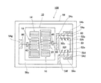
図1に示すように、本実施形態に係る弾性表面波デバイス(以下、単にSAWデバイス10と称す)は、水晶基板12と、この水晶基板12上に形成された2つのSAW共振子(第1の共振子(第1の振動子)14、第2の共振子(第2の振動子)16)を基本として構成される。第1の共振子14と第2の共振子16は互いにIDT18,28、反射器24,34を基本として構成され、引出電極38を介して入出力電極40に接続される。
As shown in FIG. 1, a surface acoustic wave device (hereinafter simply referred to as a SAW device 10) according to the present embodiment includes a
水晶基板12は、オイラー角表示で(−1.5°≦φ≦+1.5°,117°≦θ≦142°,42.79°≦|ψ|≦49.75°)で表される面内回転STカット水晶基板を採用している。なお、オイラー角(0°、0°、0°)で表される基板は、Z軸に垂直な主面を有するZカット基板となる。ここで、オイラー角(φ、θ、ψ)のφは、Zカット基板の第1の回転に関するものであり、Z軸を回転軸とし、+X軸から+Y軸側へ回転する方向を正の回転角度とした第1回転角度である。θは、Zカット基板の第1の回転後に行う第2の回転に関するものであり、第1の回転後のX軸(=X´軸)を回転軸とし、第1の回転後の+Y軸(=+Y´軸)から+Z軸へ回転する方向を正の回転角度とした第2の回転角度である。圧電基板のカット面は、第1回転角度φと第2回転角度θとで決定される。ψは、Zカット基板の第2の回転後に行う第3の回転に関するものであり、第2の回転後のZ軸(=Z´軸)を回転軸とし、第2の回転後の+X軸(=+X´軸)から第2の回転後の+Y軸(+Y´´軸)側へ回転する方向を正の回転角度とした第3回転角度である。SAWの伝搬方向は、第2の回転後のX軸(=X´軸)に対する第3回転角度ψで表される。
The
本実施形態においてIDT18とIDT28は互いに、1つの水晶基板12上に形成されている。各IDT18,28は、一対の櫛歯状電極を備える。櫛歯状電極は、複数の電極指20,30の基端部をそれぞれバスバー22,32で接続して成る。IDT18,28は、櫛歯状電極における電極指20,30同士をかみ合わせるように配置すると共に、隣接する電極指20,30間に所定の間隔が設けられるように櫛歯状電極を組み合わせることで構成される。本実施形態では、櫛歯状電極を構成する電極指20,30のバスバー22,32からの延出方向は、水晶の結晶軸であるX軸から傾きを持ったX´軸に直交するように設けられる。第1の共振子14、第2の共振子16で励起されるSAWは、Rayleigh型のSAWであり、Z´軸とX´´軸の両方に振動変位成分を有する。そしてこのようにSAWの伝播方向を水晶の結晶軸であるX軸からずらすことで、ストップバンドの上端モードのSAWを励起することが可能となる。また、本願発明者はこのように、水晶基板のカット角をオイラー角表示で(−1.5°≦φ≦+1.5°,117°≦θ≦142°,42.79°≦|ψ|≦49.75°)とした上で、ストップバンドの上端モードを用いることで、SAW共振子において3次関数で示すことのできる周波数温度特性を得ることができることを確認した。
In the present embodiment, the
反射器24,34は、各IDT18,28をSAWの伝播方向に挟み込むように一対ずつ設けられる。具体的構成としては、IDT18,28を構成する電極指20,30と平行に設けられる複数の導体ストリップ26,36の両端をそれぞれ接続したものである。複数の導体ストリップ26,36をそれぞれ接続する位置は必ずしも両端である必要はなく、一端のみで接続する形態や、一端と他端との間の何れかの位置で接続する形態などであっても良い。
A pair of
なお、水晶基板12のSAW伝播方向の端面からの反射波を積極的に利用する端面反射型SAW共振子や、IDTの電極指対数を多くすることでIDT自体でSAWの定在波を励起する多対IDT型SAW共振子においては、反射器は必ずしも必要では無い。
Note that the SAW standing wave is excited by the IDT itself by increasing the number of electrode finger pairs of the end surface reflection type SAW resonator that actively uses the reflected wave from the end surface of the
入出力電極40は、入力ポート(または出力ポート)用と出力ポート(または入力ポート)用に、一対設けられたパターン電極である。
引出電極38は、2つのIDT18,28と一対の入出力電極40とを電気的に並列に接続するパターン電極である。本実施形態では、入出力電極40を介して印加された電圧により2つのIDT18,28にて励起される双方のSAWの位相が、一致または略一致するように、引出電極38が配される。これらのIDT18,28、反射器24,34、入出力電極40、および引出電極38等を構成するパターン電極は、アルミニウム(Al)や、Alを主体とした合金を構成材料として用いることができる。
The input /
The
本実施形態に係るSAWデバイス10は、IDT18(具体的には櫛歯状電極)を構成する複数の電極指20の間、およびIDT28を構成する複数の電極指30の間に溝を設けている。溝深さGはSAWデバイスの3次温度係数γに影響を及ぼし、一般的には、3次温度係数の値(絶対値)が小さいほど、周波数温度特性が良好となることが知られている。
In the
図2は、図1に示した本実施形態に係るSAWデバイス10におけるIDT18を構成する電極指20と、IDT28を構成する電極指30の部分断面拡大図である。図2中λは、IDT18、およびIDT28におけるSAWの波長を示す。また、L1は電極指20の幅、L2は電極指30の幅を示し、S1は隣接する電極指20間に形成される溝の幅、S2は隣接する電極指30間に形成される溝の幅を示す。さらに、G1はIDT20における溝深さ、G2はIDT30における溝深さを示し、H1はIDT20における電極膜厚、H2はIDT30における電極膜厚を示す。なお、以下に示すライン占有率η(η1,η2)とは、電極指の幅L(L1,L2),を電極指間のピッチλ/2(=L1+S1またはL2+S2)で除して得られる値である。
FIG. 2 is an enlarged partial cross-sectional view of the
3次温度係数γと溝深さGとの関係は、オイラー角表示で第3回転角度を示すψについて、|42°〜45°|の範囲で、周波数温度特性が最も良好となる角度を適宜選択してシミュレーションを実施することで、図3から図5に示すようなグラフを得ることができる。なお、図3から図5において横軸は、弾性表面波の波長λに対する溝深さGの割合を示し、縦軸は、3次温度係数γの値を示す。また、図3は励振電極を構成する電極の膜厚(電極膜厚H)を0.02λとした場合の例を示すグラフである。また、図4は励振電極を構成する電極の膜厚(電極膜厚H)を0.03λとした場合の例を示すグラフである。また、図5は励振電極を構成する電極の膜厚(電極膜厚H)を0.04λとした場合の例を示すグラフである。 The relationship between the third-order temperature coefficient γ and the groove depth G is determined by appropriately setting an angle at which the frequency temperature characteristic is the best in the range of | 42 ° to 45 ° | with respect to ψ indicating the third rotation angle in Euler angle display. By selecting and executing the simulation, graphs as shown in FIGS. 3 to 5 can be obtained. 3 to 5, the horizontal axis represents the ratio of the groove depth G to the wavelength λ of the surface acoustic wave, and the vertical axis represents the value of the third-order temperature coefficient γ. FIG. 3 is a graph showing an example in which the thickness of the electrodes constituting the excitation electrode (electrode thickness H) is 0.02λ. FIG. 4 is a graph showing an example in which the thickness of the electrodes constituting the excitation electrode (electrode thickness H) is 0.03λ. FIG. 5 is a graph showing an example in which the thickness of the electrodes constituting the excitation electrode (electrode thickness H) is 0.04λ.
電極膜厚Hを0.02λとした図3によれば、溝深さGが0.01λである点付近において、3次温度係数の正負が逆転していることを読み取ることができる。 According to FIG. 3 in which the electrode film thickness H is 0.02λ, it can be read that the sign of the third-order temperature coefficient is reversed in the vicinity of the point where the groove depth G is 0.01λ.
また、電極膜厚Hを0.03λとした図4によれば、溝深さGが0.015λである点付近において、3次温度係数の正負が逆転していることを読み取ることができる。 Further, according to FIG. 4 in which the electrode film thickness H is 0.03λ, it can be read that the sign of the third-order temperature coefficient is reversed in the vicinity of the point where the groove depth G is 0.015λ.
さらに、電極膜厚Hを0.04λとした図5によれば、溝深さGが0.013λである点付近において、3次温度係数の正負が逆転していることを読み取ることができる。 Furthermore, according to FIG. 5 in which the electrode film thickness H is 0.04λ, it can be read that the sign of the third-order temperature coefficient is reversed in the vicinity of the point where the groove depth G is 0.013λ.
また、図3から図5に示すシミュレーションによれば、溝深さGが0.01λ〜0.05λの範囲においてはいずれも、3次温度係数γが、−0.1(10−10/℃3)〜+0.1(10−10/℃3)の範囲内であることを読み取ることができる。さらに、図3から図5によれば、3次温度係数が負の値となる場合には、3次温度係数が正の値となる場合に比べ、溝深さGが浅くなるということを読み取ることができる。 Further, according to the simulations shown in FIGS. 3 to 5, the third-order temperature coefficient γ is −0.1 (10 −10 / ° C.) when the groove depth G is in the range of 0.01λ to 0.05λ. 3 ) to +0.1 (10 −10 / ° C. 3 ). Further, according to FIGS. 3 to 5, it is read that when the third-order temperature coefficient is a negative value, the groove depth G is shallower than when the third-order temperature coefficient is a positive value. be able to.
なお、図3から図5に示すグラフを得るためのシミュレーションは、IDTにおける電極指の対数が210対、反射器の導体ストリップが97本(片側当たり)のSAW共振子をモデルとして行った。 In addition, the simulation for obtaining the graphs shown in FIGS. 3 to 5 was performed using a SAW resonator having 210 pairs of electrode fingers and 97 conductor strips (per side) in the IDT as a model.
また、電極指の対数、導体ストリップの本数を共通とし、電極膜厚を0.02λ、溝深さGを0.05λとしたSAW共振子をモデルとして、ライン占有率ηと、変曲点Tiとの関係のシミュレーションを実施した結果、図6に示すようなグラフを得ることができた。図6によれば、ライン占有率ηの変動に応じて変曲点Tiの値が、対数関数的に変化することを読み取ることができる。さらに、変曲点Tiの変動は、ライン占有率ηが0.63未満である場合には急激な変化を示し、0.63以上では、穏やかな変化を示すことも読み取ることができる。なお、溝深さGが0.05λ以外の場合でも、ライン占有率ηにより変曲点Tiを変えることができる。 Further, using a SAW resonator with a common number of electrode fingers and the number of conductor strips, an electrode film thickness of 0.02λ, and a groove depth G of 0.05λ as a model, a line occupancy η and an inflection point Ti As a result of performing a simulation of the relationship with the graph, a graph as shown in FIG. 6 was obtained. According to FIG. 6, it can be read that the value of the inflection point Ti changes in a logarithmic function according to the change in the line occupancy η. Further, it can be read that the fluctuation of the inflection point Ti shows a rapid change when the line occupancy η is less than 0.63, and shows a gentle change when the line occupation ratio η is 0.63 or more. Even when the groove depth G is other than 0.05λ, the inflection point Ti can be changed by the line occupation ratio η.
これらの結果より、第1の共振子14と第2の共振子16との間において、IDT18,28を構成する電極指20,30間の溝深さGを異ならせることにより、3次温度係数の符号を互いに逆にし、周波数温度特性を示す3次曲線を逆転させることができる。
また、周波数温度特性を示す3次曲線から読み取ることのできる変曲点については、ライン占有率ηを調整することで制御することができる。
From these results, the third-order temperature coefficient is obtained by making the groove depth G between the
Further, the inflection point that can be read from the cubic curve indicating the frequency temperature characteristic can be controlled by adjusting the line occupancy η.
よって、第1の共振子14における周波数温度特性と、第2の共振子16における周波数温度特性の3次温度係数の符号の正負を互いに逆の関係とし、これを結合させることによれば、フラットな、すなわち周波数変動量の少ない周波数温度特性を得ることができる。ここで、第1の共振子14における3次温度係数を−γ1、第2の共振子16における3次温度係数をγ2とし、γ1、γ2はそれぞれ、γ1>0かつγ2>0の要件を満たすものとする。図3から図5に示すグラフからも読み取れるように、第1の共振子14における3次温度係数が負の値であり、第2の共振子34における3次温度係数が正の値である場合、第1の共振子14における溝深さG1と第2の共振子16における溝深さG2との関係は、G1<G2の関係を満たすこととなる。
Therefore, the frequency temperature characteristic in the
図7に示すグラフは、オイラー角表示で(0°、123°、43.6°)のカット角の水晶基板12を用いたSAWデバイス10における第1の共振子14と第2の共振子16の周波数温度特性を示すものである。図7に示す例の場合、第1の共振子14におけるIDT18の電極膜厚H1は0.03λ、溝深さG1は0.010λ、ライン占有率η1は0.69である(図中実線)。一方、第2の共振子16におけるIDT28の電極膜厚H2は0.02λ、溝深さG2は0.045λ、ライン占有率η2は0.064である(図中破線)。なお、溝深さG1,G2と電極膜厚H1,H2、および波長λの関係、並びにライン占有率η1,η2を求めるために必要とされる電極指幅L1,L2並びに溝幅S1,S2の関係については、図2に示す。
The graph shown in FIG. 7 shows the
図7のように示される第1の共振子14の周波数温度特性と第2の共振子16の周波数温度特性を合成すると、周波数温度特性は、図8に示すようなものとなる。すなわち、−40℃〜+85℃までの温度帯域における周波数変動量が、わずか2.5ppm程度となる。よって、本実施形態に係るSAWデバイス10は、従来のSAWデバイスに比べ、周波数温度特性を飛躍的に向上させることができると言える。
When the frequency temperature characteristic of the
ところで、本実施形態に係るSAWデバイス10では、第1の共振子14の周波数温度特性と、第2の共振子16の周波数温度特性を合成することで、SAWデバイス10としての周波数温度特性を得ることとなる。このため、第1の共振子14の周波数温度特性と第2の共振子16の周波数温度特性とを示す傾き、すなわち3次温度係数が等しい場合であっても、両者の変曲点がずれた場合には周波数温度特性が悪化してしまう可能性がある。よって、2つのSAW共振子間における変曲点Tiの差分温度の許容範囲について検討する。
By the way, in the
図9に示すグラフは、図8(図7)の周波数温度特性を示す第1の共振子14と第2の共振子16における変曲点Tiのずれ量(変曲点の差分温度)と、変曲点Tiのずれによって生ずる周波数変動量の多寡を示すものである。図9によれば、変曲点Tiの差分温度が19℃以内であれば、SAWデバイスとしての周波数温度特性の周波数変動量は、10ppm以内とすることができることが判る。つまり、変曲点Tiの差分温度が19℃以内であれば、3次温度係数が著しく大きいような場合であっても、従来技術よりもさらに周波数温度特性を向上させるといった本願の課題を解決することができる。
The graph shown in FIG. 9 shows the shift amount of the inflection point Ti (difference temperature at the inflection point) in the
また、当然に、第1の共振子14の3次温度係数−γ1と第2の共振子16の3次温度係数γ2の絶対値が異なる場合には、3次曲線として示される周波数温度特性の合成時における打ち消しに偏りが生じ、SAWデバイス10としての周波数温度特性は悪化することとなる。よって、2つのSAW共振子間における3次温度係数γの関係についての許容範囲について検討する。
Also, of course, when the absolute value of the third order temperature coefficient gamma 2 cubic temperature coefficient-gamma 1 and the
図10は、第1の共振子14の3次温度係数−γ1と、第2の共振子16の3次温度係数γ2との比率と、周波数変動量の関係を示すグラフである。図10からはまず、γ1=γ2の場合、すなわちγ1/γ2=1の場合、周波数変動量が0ppmとなることが判る。また、図10からは、γ1/γ2>0、およびγ1/γ2≦2.4の範囲、すなわち0<|γ1|≦|2.4γ2|の範囲であれば、合成された周波数温度特性における周波数変動量が、10ppm以内となることを読み取ることができる。
Figure 10 is a graph showing a cubic temperature coefficient-gamma 1 of the
このような構成のSAWデバイス10であれば、−40℃から+85℃といった動作温度範囲内における周波数変動量を10ppm以内に抑えることができ、従来に比べて周波数温度特性を飛躍的に向上させることができる。
With the
なお、図1に示す形態では、単一の水晶基板12を平面視した際に、第1の共振子14と第2の共振子16との間に段差を設けることで、第1の共振子14と第2の共振子16との間における溝深さG(G1、G2)に差をつけるように示した。このような構成とした場合、段差部分にて、第1の共振子14と第2の共振子16との間を伝播する不要波を抑圧することができる。また、当該段差部分は、第1の共振子14と第2の共振子16との間における不要な音響結合を低減するといった効果も奏することとなる。
In the embodiment shown in FIG. 1, when the
しかしながら水晶基板12に段差を設ける構成は必須要素ではなく、本実施形態に係るSAWデバイス10は、図11に示すように、水晶基板12をフラットとした上で、電極形成部をエッチングすることで溝深さGに変化を与えるようにしても良い。なお、このような構成とした場合、2つの共振子間に生ずる段差は、引出電極38に位置させると良い。
However, the configuration in which the step is provided on the
また、上記実施形態に係るSAWデバイス10は、単一の水晶基板12上に第1の共振子14と第2の共振子16の双方を形成する構成としていた。しかしながら、本発明に係る圧電デバイスは、第1の共振子と第2の共振子とを異なる基板により形成し、これらを電気的に接続する形態としても良い。このような構成とした場合であっても同様な効果を得ることができるからである。
Further, the
具体的には、設計上の3次温度係数が−γ1となる第1の共振子を製造する工程と、設計上の3次温度係数がγ2となる第2の共振子を製造する工程とを有する。なお、第1の共振子の製造ラインと、第2の共振子の製造ラインとは、同一ラインであっても個別ラインであっても良い。 Specifically, a step of manufacturing a first resonator having a designed third-order temperature coefficient of -γ 1 and a step of manufacturing a second resonator having a designed third-order temperature coefficient of γ 2 And have. The first resonator manufacturing line and the second resonator manufacturing line may be the same line or individual lines.
製造された第1の共振子群と第2の共振子群は、各々変曲点Tiと3次温度係数γが計測される。その後、変曲点Tiと3次温度係数γが計測された第1の共振子群と第2の共振子群の中から、2つの共振子における変曲点Tiの差が19℃以下であり、第1の共振子における3次温度係数−γ1と第2の共振子における3次温度係数γ2との関係が、0<|γ1|≦|2.4γ2|の関係を満たす組み合わせを選択する。ここで、選択される2つの共振子は、変曲点Tiの差が0に近似し、第1の共振子の3次温度係数−γ1と第2の共振子の3次温度係数γ2との絶対値が近似する関係となることが望ましい。
The manufactured first resonator group and second resonator group are measured for an inflection point Ti and a third-order temperature coefficient γ, respectively. Thereafter, the difference between the inflection points Ti in the two resonators is 19 ° C. or less from the first resonator group and the second resonator group in which the inflection point Ti and the third-order temperature coefficient γ are measured. The combination of the third-order temperature coefficient −γ 1 in the first resonator and the third-order temperature coefficient γ 2 in the second resonator satisfies the
第1の共振子と第2の共振子を選択した後、入出力電極に対し、2つの共振子が並列な関係となるように電気的に接続する。
このような方法で圧電デバイスを構成することによれば、単一基板上に2つの共振子を構成する場合に比べ、変曲点Tiの差、および3次温度係数γの関係が最適となるように組み合わせることが可能となり、歩留まりを向上させることができる。
After selecting the first resonator and the second resonator, the input and output electrodes are electrically connected so that the two resonators are in parallel.
By configuring the piezoelectric device by such a method, the relationship between the inflection point Ti and the third-order temperature coefficient γ is optimal compared to the case where two resonators are configured on a single substrate. Thus, the yield can be improved.
また、上記実施形態では、基板として、水晶基板12を採用する旨記載した。しかしながら、本発明に係る圧電デバイスは、3次温度係数を得ることのできる構成であれば、基板の構成素材を水晶とする必要は無い。例えば、SAWを励起することのできるタンタル酸リチウムや、ニオブ酸リチウム等としても良い。
Moreover, in the said embodiment, it described that the
また、上記実施形態では、第1の振動子、第2の振動子共にSAW共振子として説明した。しかしながら、本発明に係る振動デバイスは、周波数温度特性が3次曲線を示す振動子であって、第1の振動子における3次温度係数−γ1と第2の振動子における3次温度係数γ2とが0<|γ1|≦|2.4γ2|の関係を満たせば、その形態を特に問うものでは無い。例えば、第1の振動子が、3次温度係数−γ1のATカット振動子であり、第2の振動子が3次温度係数γ2のSAW共振子であっても良い。 In the above embodiment, the first and second vibrators have been described as SAW resonators. However, the vibrating device according to the present invention is a vibrator whose frequency-temperature characteristic shows a cubic curve, and the third-order temperature coefficient −γ 1 in the first vibrator and the third-order temperature coefficient γ in the second vibrator. As long as 2 satisfies the relationship of 0 <| γ 1 | ≦ | 2.4γ 2 |, the form is not particularly questioned. For example, the first oscillator is a AT-cut resonator of the third-order temperature coefficient-gamma 1, the second oscillator may be a SAW resonator of the third-order temperature coefficient gamma 2.
また、本発明に係る振動デバイスは、図12に示すように、コンデンサを設けても良い。このような構成とする場合、第1の振動子14aと第2の振動子16a、およびコンデンサ70は、入力(出力)端子と出力(入力)端子に対して並列となるように接続すると良い。このような構成とすることで、コンデンサ70の容量により、第1の振動子14aと第2の振動子16aの結合度を変化させることができる。
Further, the vibration device according to the present invention may be provided with a capacitor as shown in FIG. In such a configuration, the
また、上記実施形態に係る振動デバイスは、いずれも第1の振動子(第1の共振子14)と第2の振動子(第2の共振子16)を電気的に並列となるように接続する旨説明した。しかしながら本発明に係る振動デバイスは、図13に示すように、入力(出力)端子と出力(入力)端子に対して直列接続となるように第1の振動子14aと第2の振動子16aを配置しても良い。さらにこのような接続形態を採った場合には、同図に示すように、第1の振動子14aと第2の振動子16aのそれぞれに対して並列となるようにインダクタ72を設けるようにしても良い。インダクタ72を接続することによれば、インダクタ72の値を変化させることで、第1の振動子14aと第2の振動子16aの結合度を変化させることができるからである。
In each of the vibrating devices according to the above-described embodiments, the first vibrator (first resonator 14) and the second vibrator (second resonator 16) are connected in parallel to each other. Explained. However, in the vibrating device according to the present invention, as shown in FIG. 13, the
次に、本発明に係るSAW発振器について、図14を参照して説明する。本発明に係るSAW発振器は図14に示すように、上述したSAWデバイス10と、このSAWデバイス10に形成された第1の共振子14、第2の共振子16を構成するIDT18,28に電圧を印加して駆動制御するIC(integrated circuit)50と、これらを収容するパッケージ56とを備える。
Next, a SAW oscillator according to the present invention will be described with reference to FIG. As shown in FIG. 14, the SAW oscillator according to the present invention has a voltage applied to the above-described
実施形態に係るSAW発振器100では、SAWデバイス10とIC50とを同一のパッケージ56に収容し、パッケージ56の底板56aに形成された電極パターン54a〜54gとSAWデバイス10に形成された入出力電極40、およびIC50のパッド52a〜52fとを金属ワイヤ60により接続している。そして、SAWデバイス10とIC50とを収容したパッケージ56のキャビティは、リッド(不図示)により気密に封止している。このような構成とすることで、IDT18,28とIC50、及びパッケージ56の底面に形成された図示しない外部実装電極とを電気的に接続することができる。
In the
また、本発明に係るSAW共振子は、携帯電話やハードディスク、サーバコンピュータ、および有線・無線基地におけるクロック源として用いることができ、本発明に係る電子機器は、これらの携帯電話やハードディスク等に、上述したSAW共振子を搭載したものをいう。 The SAW resonator according to the present invention can be used as a clock source in a mobile phone, a hard disk, a server computer, and a wired / wireless base, and the electronic device according to the present invention can be used in such a mobile phone, a hard disk, etc. This means a device equipped with the SAW resonator described above.
上記実施形態では、振動デバイスとして特に、弾性表面波を励起する圧電デバイスを例に挙げ、従来技術に比して周波数温度特性の向上が図れる旨を説明した。しかしながら本願の思想は圧電以外の駆動方式による振動デバイスにも適用することができる。例えば、クーロン力による静電駆動による振動子や、シリコン半導体を用いたMEMS振動子等であっても、3次関数温度特性を備え、3次温度係数の符号が互いに逆となる2つの振動子であれば、本発明を適用することができる。 In the above-described embodiment, a piezoelectric device that excites a surface acoustic wave as an example of the vibration device is taken as an example, and it has been described that the frequency temperature characteristics can be improved as compared with the conventional technology. However, the idea of the present application can also be applied to a vibration device using a driving method other than piezoelectric. For example, even if the vibrator is electrostatically driven by Coulomb force, the MEMS vibrator using a silicon semiconductor, or the like, two vibrators having a cubic function temperature characteristic and signs of the cubic temperature coefficient are opposite to each other. If so, the present invention can be applied.
10………SAWデバイス、12………水晶基板、14………第1の共振子、16………第2の共振子、18………IDT、20………電極指、22………バスバー、24………反射器、26………導体ストリップ、28………IDT、30………電極指、32………バスバー、34………反射器、36………導体ストリップ、38………引出電極、40………入出力電極。
10 ......... SAW device, 12 ......... Quartz substrate, 14 ......... First resonator, 16 ......... Second resonator, 18 ......... IDT, 20 ...... Electrode finger, 22 ... ... Bus bar, 24 ... …… Reflector, 26 ......... Conductor strip, 28 ......... IDT, 30 ... …… Electrode finger, 32 ......... Bus bar, 34 ... …… Reflector, 36 ... …… Conductor strip, 38... Extraction electrode, 40.
Claims (12)
前記第1の振動子に接続され、3次関数温度特性を備え前記3次関数温度特性における3次温度係数がγ2でありγ2>0である第2の振動子とを備え、
前記第1の振動子と前記第2の振動子とは、オイラー角(−1.5°≦φ≦+1.5°,117°≦θ≦142°,42.79°≦|ψ|49.75°)の水晶基板上に設けられ、ストップバンドの上端モードの弾性表面波を励起する弾性表面波共振子であり、
前記弾性表面波を励起する励振電極を構成する電極指の間に位置する前記水晶基板の部分にある電極指間の溝を備え、
前記第1の振動子の3次関数温度特性の変曲点となる温度と、前記第2の振動子の3次関数温度特性の変曲点となる温度との差の絶対値が19℃以下であり、
0<|γ1|≦|2.4γ2|
の関係を満たすと共に、
前記第1の振動子における前記電極指間の溝深さをG 1 、前記第2の振動子における前記電極指間の溝深さをG 2 として、
G 1 <G 2
の関係を満たすことを特徴とする振動デバイス。 A first vibrator having a cubic function temperature characteristic and a cubic temperature coefficient in the cubic function temperature characteristic of −γ 1 and γ 1 >0;
A second vibrator connected to the first vibrator and having a cubic function temperature characteristic, wherein a cubic temperature coefficient in the cubic function temperature characteristic is γ 2 and γ 2 > 0,
The first vibrator and the second vibrator have Euler angles (−1.5 ° ≦ φ ≦ + 1.5 °, 117 ° ≦ θ ≦ 142 °, 42.79 ° ≦ | ψ | 49. 75 °) a surface acoustic wave resonator provided on a quartz substrate for exciting a surface acoustic wave in an upper end mode of a stop band,
A groove between the electrode fingers in the portion of the quartz substrate located between the electrode fingers constituting the excitation electrode for exciting the surface acoustic wave;
The absolute value of the difference between the temperature that is the inflection point of the cubic function temperature characteristic of the first vibrator and the temperature that is the inflection point of the cubic function temperature characteristic of the second vibrator is 19 ° C. or less. And
0 <| γ 1 | ≦ | 2.4γ 2 |
Along with satisfying the relationship,
The groove depth between the electrode fingers in the first vibrator is G 1 , and the groove depth between the electrode fingers in the second vibrator is G 2 ,
G 1 <G 2
A vibration device characterized by satisfying the above relationship .
前記第1の振動子に接続され、3次関数温度特性を備え前記3次関数温度特性における3次温度係数がγ2でありγ2>0である第2の振動子とを備え、
前記第1の振動子の3次関数温度特性の変曲点となる温度と、前記第2の振動子の3次関数温度特性の変曲点となる温度との差の絶対値が19℃以下であり、
0<|γ1|≦|2.4γ2|
の関係を満たし、
前記第1の振動子と前記第2の振動子とが電気的に並列に接続されていることを特徴とする振動デバイス。 A first vibrator having a cubic function temperature characteristic and a cubic temperature coefficient in the cubic function temperature characteristic of −γ 1 and γ 1 >0;
A second vibrator connected to the first vibrator and having a cubic function temperature characteristic, wherein a cubic temperature coefficient in the cubic function temperature characteristic is γ 2 and γ 2 > 0,
The absolute value of the difference between the temperature that is the inflection point of the cubic function temperature characteristic of the first vibrator and the temperature that is the inflection point of the cubic function temperature characteristic of the second vibrator is 19 ° C. or less. And
0 <| γ 1 | ≦ | 2.4γ 2 |
Meet the relationship,
The vibrating device, wherein the first vibrator and the second vibrator are electrically connected in parallel .
前記第1の振動子に接続され、3次関数温度特性を備え前記3次関数温度特性における3次温度係数がγ2でありγ2>0である第2の振動子とを備え、
前記第1の振動子の3次関数温度特性の変曲点となる温度と、前記第2の振動子の3次関数温度特性の変曲点となる温度との差の絶対値が19℃以下であり、
0<|γ1|≦|2.4γ2|
の関係を満たし、
前記第1の振動子と前記第2の振動子とを電気的に直列に接続し、かつ前記第1の振動子と前記第2の振動子のそれぞれに対し、電気的に並列となるようにインダクタを接続していることを特徴とする振動デバイス。 A first vibrator having a cubic function temperature characteristic and a cubic temperature coefficient in the cubic function temperature characteristic of −γ 1 and γ 1 >0;
A second vibrator connected to the first vibrator and having a cubic function temperature characteristic, wherein a cubic temperature coefficient in the cubic function temperature characteristic is γ 2 and γ 2 > 0,
The absolute value of the difference between the temperature that is the inflection point of the cubic function temperature characteristic of the first vibrator and the temperature that is the inflection point of the cubic function temperature characteristic of the second vibrator is 19 ° C. or less. And
0 <| γ 1 | ≦ | 2.4γ 2 |
Meet the relationship,
The first vibrator and the second vibrator are electrically connected in series, and are electrically parallel to each of the first vibrator and the second vibrator. A vibration device characterized by connecting an inductor .
前記第1の振動子と前記第2の振動子とを単一の前記水晶基板上に設けたことを特徴とする振動デバイス。 The vibrating device according to claim 1 ,
A vibrating device, wherein the first vibrator and the second vibrator are provided on a single quartz substrate.
前記圧電基板上に段差を備え、
前記段差は、前記水晶基板を平面視して前記第1の振動子と前記第2の振動子との間に設けることを特徴とする振動デバイス。 The vibrating device according to claim 4 ,
Provided with a step on the piezoelectric substrate,
The vibration step is provided between the first vibrator and the second vibrator in a plan view of the crystal substrate.
前記第1の振動子と前記第2の振動子とが電気的に並列に接続されていることを特徴とする振動デバイス。 The vibration device according to any one of claims 1, 4, and 5 ,
The vibrating device, wherein the first vibrator and the second vibrator are electrically connected in parallel.
電気的に並列に接続された前記第1の振動子と前記第2の振動子と電気的に並列となるようにコンデンサを接続したことを特徴とする振動デバイス。 The vibrating device according to claim 2 or 6 ,
A vibrating device, wherein a capacitor is connected so as to be electrically parallel to the first vibrator and the second vibrator electrically connected in parallel.
前記第1の振動子と前記第2の振動子とが電気的に直列に接続されていることを特徴とする振動デバイス。 The vibrating device according to claim 1 ,
The vibrating device, wherein the first vibrator and the second vibrator are electrically connected in series.
電気的に直列に接続された前記第1の振動子と前記第2の振動子のそれぞれに対し、電気的に並列となるようにインダクタを接続したことを特徴とする振動デバイス。 The vibration device according to claim 8 ,
An oscillating device, wherein an inductor is connected to each of the first vibrator and the second vibrator electrically connected in series so as to be electrically in parallel.
発振回路とを有することを特徴とする発振器。 The vibration device according to any one of claims 1 to 9 ,
An oscillator comprising an oscillation circuit.
オイラー角(−1.5°≦φ≦+1.5°,117°≦θ≦142°,42.79°≦|ψ|49.75°)の水晶基板上に3次関数温度特性を備え前記3次関数温度特性における3次温度係数が−γ2でありγ2>0であり、ストップバンドの上端モードの弾性表面波を励起する弾性表面波共振子であって、前記弾性表面波を励起する励振電極を構成する電極指の間に位置する前記水晶基板の部分にある電極指間の溝を備える第2の振動子を製造する工程と、
製造された第1の振動子群と第2の振動子群の中から、前記3次関数温度特性の変曲点となる温度の差が19℃以下であり、
0<|γ2|≦|2.4γ1|
の関係および、
前記第1の振動子における前記電極指間の溝深さをG 1 、前記第2の振動子における前記電極指間の溝深さをG 2 として、
G 1 <G 2
の関係を満たす前記第1の振動子と前記第2の振動子の組み合わせを選定する工程と、
選定された前記第1の振動子と前記第2の振動子とを接続する工程とを有することを特徴とする振動デバイスの製造方法。 A cubic function temperature characteristic is provided on a quartz substrate with Euler angles (−1.5 ° ≦ φ ≦ + 1.5 °, 117 ° ≦ θ ≦ 142 °, 42.79 ° ≦ | ψ | 49.75 °). cubic function cubic temperature coefficient in the temperature characteristic is gamma 1 gamma 1> than zero der, a surface acoustic wave resonator for exciting a surface acoustic wave in the upper mode of the stop band, exciting the surface acoustic wave Producing a first vibrator comprising a groove between electrode fingers in a portion of the quartz crystal substrate located between electrode fingers constituting excitation electrodes to be
A cubic function temperature characteristic is provided on a quartz substrate with Euler angles (−1.5 ° ≦ φ ≦ + 1.5 °, 117 ° ≦ θ ≦ 142 °, 42.79 ° ≦ | ψ | 49.75 °). cubic function cubic temperature coefficient in the temperature characteristic is-gamma 2 gamma 2> than zero der, a surface acoustic wave resonator for exciting a surface acoustic wave in the upper mode of the stop band, the surface acoustic wave Producing a second vibrator comprising a groove between electrode fingers in a portion of the quartz substrate located between electrode fingers constituting excitation electrodes to be excited ;
From the manufactured first vibrator group and second vibrator group, a temperature difference that is an inflection point of the cubic function temperature characteristic is 19 ° C. or less,
0 <| γ 2 | ≦ | 2.4γ 1 |
Relationship and
The groove depth between the electrode fingers in the first vibrator is G 1 , and the groove depth between the electrode fingers in the second vibrator is G 2 ,
G 1 <G 2
Selecting a combination of the first vibrator and the second vibrator satisfying the relationship :
A method for manufacturing a vibrating device, comprising: connecting the selected first vibrator and the second vibrator.
Priority Applications (3)
| Application Number | Priority Date | Filing Date | Title |
|---|---|---|---|
| JP2010272914A JP5648908B2 (en) | 2010-12-07 | 2010-12-07 | Vibration device, oscillator, and electronic device |
| CN2011103994706A CN102545825A (en) | 2010-12-07 | 2011-12-05 | Vibration device, oscillator, and electronic apparatus |
| US13/312,276 US8476984B2 (en) | 2010-12-07 | 2011-12-06 | Vibration device, oscillator, and electronic apparatus |
Applications Claiming Priority (1)
| Application Number | Priority Date | Filing Date | Title |
|---|---|---|---|
| JP2010272914A JP5648908B2 (en) | 2010-12-07 | 2010-12-07 | Vibration device, oscillator, and electronic device |
Publications (3)
| Publication Number | Publication Date |
|---|---|
| JP2012124677A JP2012124677A (en) | 2012-06-28 |
| JP2012124677A5 JP2012124677A5 (en) | 2014-02-06 |
| JP5648908B2 true JP5648908B2 (en) | 2015-01-07 |
Family
ID=46161683
Family Applications (1)
| Application Number | Title | Priority Date | Filing Date |
|---|---|---|---|
| JP2010272914A Active JP5648908B2 (en) | 2010-12-07 | 2010-12-07 | Vibration device, oscillator, and electronic device |
Country Status (3)
| Country | Link |
|---|---|
| US (1) | US8476984B2 (en) |
| JP (1) | JP5648908B2 (en) |
| CN (1) | CN102545825A (en) |
Families Citing this family (10)
| Publication number | Priority date | Publication date | Assignee | Title |
|---|---|---|---|---|
| US8952596B2 (en) * | 2009-02-27 | 2015-02-10 | Seiko Epson Corporation | Surface acoustic wave resonator, surface acoustic wave oscillator, and electronic instrument |
| JP5678486B2 (en) | 2010-06-17 | 2015-03-04 | セイコーエプソン株式会社 | Surface acoustic wave resonator, surface acoustic wave oscillator and electronic device |
| JP5934464B2 (en) | 2010-08-26 | 2016-06-15 | セイコーエプソン株式会社 | Surface acoustic wave resonator, surface acoustic wave oscillator, and electronic device |
| JP2012060422A (en) | 2010-09-09 | 2012-03-22 | Seiko Epson Corp | Surface acoustic wave device, electronic apparatus and sensor device |
| JP2012060418A (en) | 2010-09-09 | 2012-03-22 | Seiko Epson Corp | Surface acoustic wave device, electronic apparatus and sensor device |
| JP2012060419A (en) | 2010-09-09 | 2012-03-22 | Seiko Epson Corp | Surface acoustic wave device, electronic apparatus and sensor device |
| JP2012060421A (en) * | 2010-09-09 | 2012-03-22 | Seiko Epson Corp | Surface acoustic wave device, electronic apparatus and sensor device |
| JP2012060420A (en) * | 2010-09-09 | 2012-03-22 | Seiko Epson Corp | Surface acoustic wave device, electronic apparatus and sensor device |
| JP5880520B2 (en) * | 2013-10-30 | 2016-03-09 | 株式会社村田製作所 | Elastic wave device and manufacturing method thereof |
| US20210111688A1 (en) * | 2019-10-10 | 2021-04-15 | Skyworks Solutions, Inc. | Surface acoustic wave device with multi-layer piezoelectric substrate |
Family Cites Families (55)
| Publication number | Priority date | Publication date | Assignee | Title |
|---|---|---|---|---|
| JPS5479548A (en) * | 1977-12-08 | 1979-06-25 | Seiko Instr & Electronics Ltd | Oscillation circuit using piezoelectic vibrator |
| JPS54156455A (en) | 1978-05-31 | 1979-12-10 | Toshiba Corp | Surface acoustic wave element and its trimming method |
| JPS575418A (en) * | 1980-06-13 | 1982-01-12 | Nippon Telegr & Teleph Corp <Ntt> | Cavity type surface elastic wave resonator |
| GB2078042B (en) | 1980-06-13 | 1984-08-08 | Nippon Telegraph & Telephone | Surface acoustic wave resonator |
| JPS5799813A (en) | 1980-12-13 | 1982-06-21 | Nippon Telegr & Teleph Corp <Ntt> | Surface acoustic wave resonator |
| JPS5833309A (en) | 1981-08-21 | 1983-02-26 | Toyo Commun Equip Co Ltd | Slip wave resonator |
| JPS6192011A (en) | 1984-10-11 | 1986-05-10 | Nec Kansai Ltd | Manufacture of surface acoustic wave element |
| JPH0640610B2 (en) | 1985-03-26 | 1994-05-25 | 和彦 山之内 | Surface acoustic wave resonator |
| JPS61220513A (en) | 1985-03-26 | 1986-09-30 | Kazuhiko Yamanouchi | Surface acoustic wave resonator |
| JPH01231412A (en) | 1988-03-11 | 1989-09-14 | Fujitsu Ltd | Method for adjusting frequency characteristic of surface acoustic wave device |
| JPH02189011A (en) | 1989-01-18 | 1990-07-25 | Fujitsu Ltd | Manufacture of surface acoustic wave device |
| JP2982208B2 (en) | 1990-03-30 | 1999-11-22 | 富士通株式会社 | Surface acoustic wave device |
| CA2038474C (en) | 1990-03-19 | 1994-09-20 | Yoshio Satoh | Surface-acoustic-waver filter having a plurality of electrodes |
| JPH0590865A (en) | 1991-09-30 | 1993-04-09 | Oki Electric Ind Co Ltd | Central frequency adjusting method for acoustic surface wave filter |
| JPH10270974A (en) | 1997-03-25 | 1998-10-09 | Kenwood Corp | Surface acoustic wave element |
| JP3266846B2 (en) | 1998-01-20 | 2002-03-18 | 東洋通信機株式会社 | Reflection inversion type surface acoustic wave converter and filter |
| JP3301399B2 (en) | 1998-02-16 | 2002-07-15 | 株式会社村田製作所 | Surface acoustic wave device |
| FR2779289B1 (en) | 1998-05-29 | 2000-09-01 | Thomson Csf | SOUND UNIDIRECTIONAL TRANSDUCER WITH SURFACE ACOUSTIC WAVES |
| JP3840852B2 (en) | 1998-10-15 | 2006-11-01 | セイコーエプソン株式会社 | Surface acoustic wave device and 2-port surface acoustic wave resonator |
| JP2002100959A (en) | 2000-09-25 | 2002-04-05 | Toyo Commun Equip Co Ltd | Surface acoustic wave device |
| JP3897229B2 (en) | 2001-04-27 | 2007-03-22 | 株式会社村田製作所 | Surface wave filter |
| JP3724575B2 (en) | 2001-08-09 | 2005-12-07 | セイコーエプソン株式会社 | Surface acoustic wave device |
| JP3622202B2 (en) | 2001-08-29 | 2005-02-23 | セイコーエプソン株式会社 | Method for adjusting temperature characteristics of surface acoustic wave device |
| JP2003258601A (en) | 2001-12-28 | 2003-09-12 | Seiko Epson Corp | Surface acoustic wave apparatus and communication device using it |
| JP2004274696A (en) * | 2002-10-04 | 2004-09-30 | Seiko Epson Corp | Surface acoustic wave device and temperature characteristic adjustment method of surface acoustic wave device |
| US7135805B2 (en) | 2003-04-08 | 2006-11-14 | Nihon Dempa Kogyo Co., Ltd. | Surface acoustic wave transducer |
| JP2005012736A (en) | 2003-06-17 | 2005-01-13 | Kazuhiko Yamanouchi | Surface acoustic wave converter and electronic device using same |
| CA2536573A1 (en) * | 2003-08-25 | 2005-05-06 | Tele Filter Gmbh | Oscillator with an acoustic surface wave resonator |
| JP2005204275A (en) | 2003-12-12 | 2005-07-28 | Seiko Epson Corp | Surface acoustic wave element piece, its manufacturing method, and surface acoustic wave device |
| JP2006074136A (en) | 2004-08-31 | 2006-03-16 | Seiko Epson Corp | Surface acoustic wave element chip and surface acoustic wave device |
| JP2006148622A (en) | 2004-11-22 | 2006-06-08 | Seiko Epson Corp | Surface acoustic wave device and electronic equipment |
| JP2006203408A (en) | 2005-01-19 | 2006-08-03 | Epson Toyocom Corp | Surface acoustic wave device |
| US7382217B2 (en) | 2004-12-03 | 2008-06-03 | Epson Toyocom Corporation | Surface acoustic wave device |
| DE102004060901A1 (en) * | 2004-12-14 | 2006-07-13 | Leibnitz-Institut für Festkörper- und Werkstoffforschung Dresden e.V. | oscillator |
| JP2006186623A (en) | 2004-12-27 | 2006-07-13 | Seiko Epson Corp | Surface acoustic wave element, manufacturing method thereof, and surface acoustic wave device |
| JP2005137031A (en) * | 2005-02-14 | 2005-05-26 | Seiko Epson Corp | Saw device, temperature characteristic adjustment method for oscillator circuit and oscillator |
| JP2006295311A (en) | 2005-04-06 | 2006-10-26 | Seiko Epson Corp | Surface acoustic wave element chip and surface acoustic wave device |
| JP3851336B1 (en) | 2005-05-31 | 2006-11-29 | 隆彌 渡邊 | Surface acoustic wave device |
| US7868522B2 (en) * | 2005-09-09 | 2011-01-11 | Avago Technologies Wireless Ip (Singapore) Pte. Ltd. | Adjusted frequency temperature coefficient resonator |
| JP4569447B2 (en) | 2005-11-18 | 2010-10-27 | エプソントヨコム株式会社 | Surface acoustic wave element and surface acoustic wave device |
| JP4412292B2 (en) | 2006-02-06 | 2010-02-10 | セイコーエプソン株式会社 | Surface acoustic wave device and electronic apparatus |
| JP2007259414A (en) | 2006-02-24 | 2007-10-04 | Seiko Epson Corp | Method for fabricating elastic surface wave equipment, method for ajusting its temperature characteristics, and elastic surface wave equipment manufactured thereby |
| JP2007267033A (en) | 2006-03-28 | 2007-10-11 | Epson Toyocom Corp | Surface acoustic wave element and surface acoustic wave device |
| JP5141856B2 (en) | 2006-04-04 | 2013-02-13 | セイコーエプソン株式会社 | Method for manufacturing surface acoustic wave device and surface acoustic wave device |
| JP4968510B2 (en) | 2006-04-27 | 2012-07-04 | セイコーエプソン株式会社 | Method for adjusting frequency-temperature characteristics of surface acoustic wave element piece, surface acoustic wave element piece, and surface acoustic wave device |
| JP2007300287A (en) | 2006-04-28 | 2007-11-15 | Epson Toyocom Corp | Surface acoustic wave element, surface acoustic wave device, and electronic apparatus |
| DE102006027060B4 (en) | 2006-06-08 | 2010-04-01 | Leibniz-Institut Für Festkörper- Und Werkstoffforschung Dresden E.V. | Oscillator circuit with single-port acoustic surface wave resonators |
| JP2008078984A (en) | 2006-09-21 | 2008-04-03 | Epson Toyocom Corp | Saw device and electronic apparatus |
| JP4645957B2 (en) | 2006-09-29 | 2011-03-09 | セイコーエプソン株式会社 | Surface acoustic wave element and surface acoustic wave device |
| JP2008236295A (en) | 2007-03-20 | 2008-10-02 | Seiko Epson Corp | Saw resonator |
| JP4591800B2 (en) | 2008-02-20 | 2010-12-01 | エプソントヨコム株式会社 | Surface acoustic wave device and surface acoustic wave oscillator |
| DE102008001837A1 (en) * | 2008-05-17 | 2009-12-03 | Leibniz-Institut Für Festkörper- Und Werkstoffforschung Dresden E.V. | Temperature stable double resonator for use as e.g. sensor, has resonators including temperature coefficients of resonance or anti-resonance frequency whose deflection according to angle forms converter direction with rotation axis |
| US8952596B2 (en) * | 2009-02-27 | 2015-02-10 | Seiko Epson Corporation | Surface acoustic wave resonator, surface acoustic wave oscillator, and electronic instrument |
| JP4645923B2 (en) | 2009-02-27 | 2011-03-09 | セイコーエプソン株式会社 | Surface acoustic wave resonator and surface acoustic wave oscillator |
| JP2012060420A (en) * | 2010-09-09 | 2012-03-22 | Seiko Epson Corp | Surface acoustic wave device, electronic apparatus and sensor device |
-
2010
- 2010-12-07 JP JP2010272914A patent/JP5648908B2/en active Active
-
2011
- 2011-12-05 CN CN2011103994706A patent/CN102545825A/en active Pending
- 2011-12-06 US US13/312,276 patent/US8476984B2/en active Active
Also Published As
| Publication number | Publication date |
|---|---|
| US8476984B2 (en) | 2013-07-02 |
| US20120139652A1 (en) | 2012-06-07 |
| CN102545825A (en) | 2012-07-04 |
| JP2012124677A (en) | 2012-06-28 |
Similar Documents
| Publication | Publication Date | Title |
|---|---|---|
| JP5648908B2 (en) | Vibration device, oscillator, and electronic device | |
| JP5678486B2 (en) | Surface acoustic wave resonator, surface acoustic wave oscillator and electronic device | |
| JP5574200B2 (en) | Surface acoustic wave resonator, surface acoustic wave oscillator, and electronic device | |
| JP4591800B2 (en) | Surface acoustic wave device and surface acoustic wave oscillator | |
| JP5934464B2 (en) | Surface acoustic wave resonator, surface acoustic wave oscillator, and electronic device | |
| US8723394B2 (en) | Surface acoustic wave device, electronic apparatus, and sensor apparatus | |
| US9048806B2 (en) | Surface acoustic wave device, electronic apparatus, and sensor apparatus | |
| JP5652606B2 (en) | Surface acoustic wave resonator, surface acoustic wave oscillator, and electronic device | |
| JP2012060422A (en) | Surface acoustic wave device, electronic apparatus and sensor device | |
| JP4569447B2 (en) | Surface acoustic wave element and surface acoustic wave device | |
| JP4645957B2 (en) | Surface acoustic wave element and surface acoustic wave device | |
| JP2012060419A (en) | Surface acoustic wave device, electronic apparatus and sensor device | |
| JP2008054163A (en) | Lamb-wave type high-frequency resonator | |
| US8471434B2 (en) | Surface acoustic wave device, surface acoustic wave oscillator, and electronic apparatus | |
| JP4465464B2 (en) | Lamb wave type elastic wave device | |
| JP4582150B2 (en) | Surface acoustic wave device and module device or oscillation circuit using the same | |
| JP4148216B2 (en) | Surface acoustic wave device and module device or oscillation circuit using the same | |
| JP5850109B2 (en) | Surface acoustic wave resonator, surface acoustic wave oscillator, and electronic device | |
| JP2007088952A (en) | Surface acoustic wave device | |
| JP5737490B2 (en) | Transversal surface acoustic wave device, surface acoustic wave oscillator and electronic equipment | |
| JP5750683B2 (en) | Two-terminal-pair surface acoustic wave resonator, surface acoustic wave oscillator and electronic device | |
| JP2015084534A (en) | Two-terminal pair surface acoustic wave resonator, surface acoustic wave oscillator, and electronic apparatus | |
| JP2012060417A (en) | Surface acoustic wave device, electronic apparatus and sensor device | |
| JP2015084535A (en) | Transversal type surface acoustic wave device, surface acoustic wave oscillator, and electronic apparatus | |
| JP2015029358A (en) | Surface acoustic wave resonator, surface acoustic wave oscillator, and electronic device |
Legal Events
| Date | Code | Title | Description |
|---|---|---|---|
| A521 | Written amendment |
Free format text: JAPANESE INTERMEDIATE CODE: A523 Effective date: 20131127 |
|
| A621 | Written request for application examination |
Free format text: JAPANESE INTERMEDIATE CODE: A621 Effective date: 20131127 |
|
| A521 | Written amendment |
Free format text: JAPANESE INTERMEDIATE CODE: A523 Effective date: 20131220 |
|
| A977 | Report on retrieval |
Free format text: JAPANESE INTERMEDIATE CODE: A971007 Effective date: 20140611 |
|
| A131 | Notification of reasons for refusal |
Free format text: JAPANESE INTERMEDIATE CODE: A131 Effective date: 20140618 |
|
| A521 | Written amendment |
Free format text: JAPANESE INTERMEDIATE CODE: A523 Effective date: 20140811 |
|
| TRDD | Decision of grant or rejection written | ||
| A01 | Written decision to grant a patent or to grant a registration (utility model) |
Free format text: JAPANESE INTERMEDIATE CODE: A01 Effective date: 20141017 |
|
| A61 | First payment of annual fees (during grant procedure) |
Free format text: JAPANESE INTERMEDIATE CODE: A61 Effective date: 20141030 |
|
| R150 | Certificate of patent or registration of utility model |
Ref document number: 5648908 Country of ref document: JP Free format text: JAPANESE INTERMEDIATE CODE: R150 |
|
| S531 | Written request for registration of change of domicile |
Free format text: JAPANESE INTERMEDIATE CODE: R313531 |
|
| R350 | Written notification of registration of transfer |
Free format text: JAPANESE INTERMEDIATE CODE: R350 |