JP2005204275A - Surface acoustic wave element piece, its manufacturing method, and surface acoustic wave device - Google Patents
Surface acoustic wave element piece, its manufacturing method, and surface acoustic wave device Download PDFInfo
- Publication number
- JP2005204275A JP2005204275A JP2004242806A JP2004242806A JP2005204275A JP 2005204275 A JP2005204275 A JP 2005204275A JP 2004242806 A JP2004242806 A JP 2004242806A JP 2004242806 A JP2004242806 A JP 2004242806A JP 2005204275 A JP2005204275 A JP 2005204275A
- Authority
- JP
- Japan
- Prior art keywords
- acoustic wave
- surface acoustic
- wave element
- piece
- reflector
- Prior art date
- Legal status (The legal status is an assumption and is not a legal conclusion. Google has not performed a legal analysis and makes no representation as to the accuracy of the status listed.)
- Withdrawn
Links
Images


Classifications
-
- H—ELECTRICITY
- H03—ELECTRONIC CIRCUITRY
- H03H—IMPEDANCE NETWORKS, e.g. RESONANT CIRCUITS; RESONATORS
- H03H3/00—Apparatus or processes specially adapted for the manufacture of impedance networks, resonating circuits, resonators
- H03H3/007—Apparatus or processes specially adapted for the manufacture of impedance networks, resonating circuits, resonators for the manufacture of electromechanical resonators or networks
- H03H3/08—Apparatus or processes specially adapted for the manufacture of impedance networks, resonating circuits, resonators for the manufacture of electromechanical resonators or networks for the manufacture of resonators or networks using surface acoustic waves
-
- H—ELECTRICITY
- H03—ELECTRONIC CIRCUITRY
- H03H—IMPEDANCE NETWORKS, e.g. RESONANT CIRCUITS; RESONATORS
- H03H9/00—Networks comprising electromechanical or electro-acoustic devices; Electromechanical resonators
- H03H9/02—Details
- H03H9/02535—Details of surface acoustic wave devices
- H03H9/02543—Characteristics of substrate, e.g. cutting angles
- H03H9/02551—Characteristics of substrate, e.g. cutting angles of quartz substrates
-
- H—ELECTRICITY
- H03—ELECTRONIC CIRCUITRY
- H03H—IMPEDANCE NETWORKS, e.g. RESONANT CIRCUITS; RESONATORS
- H03H9/00—Networks comprising electromechanical or electro-acoustic devices; Electromechanical resonators
- H03H9/02—Details
- H03H9/125—Driving means, e.g. electrodes, coils
- H03H9/145—Driving means, e.g. electrodes, coils for networks using surface acoustic waves
- H03H9/14544—Transducers of particular shape or position
- H03H9/14594—Plan-rotated or plan-tilted transducers
-
- H—ELECTRICITY
- H03—ELECTRONIC CIRCUITRY
- H03H—IMPEDANCE NETWORKS, e.g. RESONANT CIRCUITS; RESONATORS
- H03H9/00—Networks comprising electromechanical or electro-acoustic devices; Electromechanical resonators
- H03H9/02—Details
- H03H9/125—Driving means, e.g. electrodes, coils
- H03H9/145—Driving means, e.g. electrodes, coils for networks using surface acoustic waves
- H03H9/14544—Transducers of particular shape or position
- H03H9/14547—Fan shaped; Tilted; Shifted; Slanted; Tapered; Arched; Stepped finger transducers
Abstract
Description
本発明は、弾性表面波を利用した弾性表面波素子片に係り、特に弾性表面波の位相速度の方向と群速度の方向とが異なっている弾性表面波素子片およびその製造方法並びに弾性表面波装置に関する。 The present invention relates to a surface acoustic wave element using surface acoustic waves, and more particularly, to a surface acoustic wave element having a phase velocity direction and a group velocity direction different from each other, a method of manufacturing the same, and a surface acoustic wave. Relates to the device.
弾性表面波(Surface Acoustic Wave:SAW)を利用した弾性表面波装置(SAWデバイス)は、水晶などの圧電平板の表面にすだれ状電極(Interdigital Transducer:IDT)を形成した弾性表面波素子片が用いられる。従来、SAWデバイスは、高周波領域における特性が優れているところから、高周波フィルタとして広く利用されていた。この高周波フィルタを構成する弾性表面波素子片は、STカット水晶板によって形成されたものが多い。 A surface acoustic wave device (SAW device) using surface acoustic wave (SAW) uses a surface acoustic wave element in which interdigital transducers (IDT) are formed on the surface of a piezoelectric flat plate such as quartz. It is done. Conventionally, SAW devices have been widely used as high frequency filters because of their excellent characteristics in the high frequency region. Many of the surface acoustic wave element pieces constituting the high-frequency filter are formed of ST-cut quartz plates.
水晶は、三方晶系の単結晶であって、相互に直交する3つの結晶軸、すなわち電気軸(X軸)と機械軸(Y軸)と光学軸(Z軸)とによって表現される。これらの結晶軸は、一般に図10のように表示される。そして、STカット水晶板10は、カット角がオイラー角(φ°,θ°,ψ°)による表示でφ°=0°、θ°=123°前後、ψ°=0°である。すなわち、図10に示したように、STカット水晶板10は、Y軸とZ軸とをX軸を中心にして反時計方向にθ°=123°程度回転させてY’軸、Z’軸とし、X軸とY’軸とがなす面に平行な面を有する水晶板として形成される。また、XY’面に直交したSTカット水晶板10の厚み方向の軸がZ’軸とされる。
Quartz is a trigonal single crystal and is expressed by three crystal axes orthogonal to each other, that is, an electric axis (X axis), a mechanical axis (Y axis), and an optical axis (Z axis). These crystal axes are generally displayed as shown in FIG. The ST
STカット水晶板10からなる弾性表面波素子片12は、周波数温度特性の一次係数が0であるため、周波数安定性に優れているところから、SAW共振子やSAWフィルタに広く利用されている。STカット水晶板10からなる弾性表面波素子片12は、図10に示してあるように、IDT14および反射器16がX軸に沿って形成される。
The surface acoustic
ところで、STカット水晶板10は、高周波発振器を構成するSAW共振子にした場合、要求される仕様を満足する特性を得ることが困難である。すなわち、弾性表面波素子片12は、SAWフィルタとして用いる場合、比較的広い周波数帯域において動作すればよいため、特定の周波数を発振する共振子のような高いQ値を必要としない。しかし、STカット水晶板10からなる弾性表面波素子片12は、一次温度係数が0であるが、2次温度係数が比較的大きい。このため、STカット水晶板10からなる弾性表面波素子片12は、SAW共振子の動作温度範囲である−20℃〜+80℃の温度範囲において、共振周波数が約100ppm程度変動することが知られており、高精度な通信装置などにおいて要求される周波数温度特性を満足することができない。
By the way, when the ST cut
そこで、本願出願人は、STカット水晶板10などを、図10に示したように、Z’軸周りにψ°回転(面内回転)、すなわちX軸とY’軸とをZ’軸周りにψ°回転させてX軸をX’軸、Y’軸をY”軸とし、カット角がオイラー角で(0°,θ°,ψ°)となる弾性表面波素子片20を用いたSAW共振子を開発した(特許文献1)。このSTカット水晶板10を面内回転させて形成した弾性表面波素子片20は、IDT14と反射器16とがX’軸に沿って形成してあり、STカット水晶板10を面内回転せずに形成した弾性表面波素子片12より二次温度係数を小さくでき、非常に優れた周波数温度特性を有する。
Therefore, the applicant of the present application, as shown in FIG. 10, rotates the ST-
ところが、STカット水晶板10を面内回転させて形成した弾性表面波素子片20は、水晶単結晶が異方性を有するために、弾性表面波の位相が伝播する方向である位相速度の方向と、波群(波束)が伝播する方向である群速度の方向とが異なる(非特許文献1)。群速度の方向は、弾性表面波のエネルギーの進む方向であって、位相速度の方向と群速度の方向とがなす角はパワーフロー角PFAと呼ばれている。そして、弾性表面波素子片は、群速度の方向に伝播した波群が反射されないと、共振子に必要とされる大きなQ値を得ることができない。このため、IDTと反射器とをX’軸に沿って形成した場合、IDTにおいて発生させた弾性表面波が反射器で効率良く反射されず、Q値が低下する。そこで、本願出願人は、特許文献1において図11に示した弾性表面波素子片30を開発した。この弾性表面波素子片30は、水晶板片32の表面に形成したIDT34と、IDT34の両側の反射器36とを群速度の方向に沿って配置し、弾性表面波を反射器36で効率良く反射させて、大きなQ値が得られるようにしている。
ところで、非特許文献1によると、面内回転させた水晶板のパワーフロー角PFA、すなわち弾性表面波の位相速度の方向と群速度の方向とのなす角PFAは、弾性表面波の位相速度をv、水晶板の面内回転角をψとした場合、

しかし、従来においては、面内回転STカット水晶板に発生させた弾性表面波の正確な位相速度が求められておらず、数式1により求めたパワーフロー角PFAに基づいた群速度の方向に沿ってIDTと反射器とを配置したものが、本当に群速度の方向に沿って配置されているのかが不明であった。
However, in the prior art, an accurate phase velocity of the surface acoustic wave generated in the in-plane rotating ST-cut quartz plate has not been obtained, and it follows the direction of the group velocity based on the power flow angle PFA obtained by
また、弾性表面波素子片は、一般に矩形状に形成される。特許文献1に記載の弾性表面波素子片30も同様であって、IDT34と一対の反射器36とを形成した水晶板片32が水晶ウエハから矩形状に切り出される。そして、水晶板片32は、長辺となる対向する二辺38、39が弾性表面波の位相速度の方向であるX’軸に沿うように切断される。このため、弾性表面波素子片30は、IDT34と反射器36との両側部に無駄な領域が形成され、水晶板片32の面積が有効な弾性表面波の伝播領域であるIDT34、反射器36の形成領域よりも必要以上に大きくなる。このため、弾性表面波素子片30は、大型になって1枚のウエハに形成できる数が少なくなり、収率が低く、コストが上昇する。
The surface acoustic wave element piece is generally formed in a rectangular shape. The same applies to the surface acoustic
本発明は、上記従来技術の欠点を解消するためになされたもので、面内回転させた水晶板の弾性表面波の群速度の方向に沿ってIDTと反射器とを確実に配置できるようにすることを目的としている。 The present invention was made to eliminate the above-mentioned drawbacks of the prior art, so that the IDT and the reflector can be reliably arranged along the direction of the group velocity of the surface acoustic wave of the quartz plate rotated in the plane. The purpose is to do.
また、本発明は、面内回転させた水晶板を用いた弾性表面波素子片のQ値を大きくできるようにすることを目的としている。
さらに、本発明は、弾性表面波素子片を小さくできるようにすることを目的としている。
そして、本発明は、収率を向上できるようにすることを目的としている。
Another object of the present invention is to increase the Q value of a surface acoustic wave element using a quartz plate rotated in-plane.
Another object of the present invention is to make the surface acoustic wave element piece small.
And this invention aims at enabling it to improve a yield.
本願発明者らは、面内回転STカット水晶板に関して鋭意研究し、有限要素法(Finite Element Method:FEM)により弾性表面波の位相速度を詳細に解析し、その位相速度を用いて面内回転STカット水晶板のパワーフロー角PFAについて検討した。その結果、面内回転STカット水晶板のパワーフロー角PFAは、水晶の電気軸であるX軸まわりの回転角θに依存していることを見いだした。本発明は、このような知見に基づいてなされたものである。 The inventors of the present application have conducted intensive research on in-plane rotation ST-cut quartz plates, analyzed the phase velocity of surface acoustic waves in detail using the Finite Element Method (FEM), and performed in-plane rotation using the phase velocity. The power flow angle PFA of the ST cut quartz plate was examined. As a result, it was found that the power flow angle PFA of the in-plane rotated ST-cut quartz plate depends on the rotational angle θ around the X axis, which is the electrical axis of the quartz crystal. The present invention has been made based on such knowledge.
すなわち、本発明に係る弾性表面波素子片は、オイラー角を(φ°,θ°,ψ°)としたときのカット角が(0°,113°〜135°,±(40°〜49°))の面内回転STカット水晶板片と、前記水晶板片の表面に形成され、前記水晶板片の弾性表面波の位相速度の方向に対して、PFA±3°傾斜した方向に沿って配置されたすだれ状電極と反射器とを有し、
前記PFAが、
The PFA is
カット角が(0°,113°〜135°,±(40°〜49°))である面内回転STカット水晶板のパワーフロー角PFAは、本願発明者らの研究によると、X軸回りの回転角をθ°とした場合、上記数式2によって求められることを突き止めた。したがって、面内回転STカット水晶板を用いた弾性表面波素子片を形成する場合、すだれ状電極(IDT)と反射器とは、弾性表面波の位相速度の方向に対して、数式2によって求めたパワーフロー角PFAを傾斜させた方向に沿って配置する。これにより、IDTと反射器とを、弾性表面波の群速度の方向に沿って確実に配置することが可能で、IDTにおいて発生させた弾性表面波の波群を、反射器によって効率よく反射することができ、Q値を高めることができる。
According to the research by the present inventors, the power flow angle PFA of the in-plane rotation ST-cut quartz plate whose cut angle is (0 °, 113 ° to 135 °, ± (40 ° to 49 °)) is around the X axis. When the rotation angle is θ °, it was found out that it is obtained by the
なお、発明者らの実験によると、IDTと反射器との配置方向が数式2によって求めたパワーフロー角PFAに対して±3°程度ずれていても、充分に大きなQ値を得ることができる。特に、IDTと反射器との配置方向は、パワーフロー角PFAに対して±1°程度ずれていても、Q値に対してほとんど影響を与えない。したがって、IDTと反射器との配置方向と、弾性表面波の位相速度の方向とのなす角は、PFA±3°に設定することができる。
According to the experiments by the inventors, a sufficiently large Q value can be obtained even if the arrangement direction of the IDT and the reflector is deviated by about ± 3 ° with respect to the power flow angle PFA obtained by
水晶板片は、対向する二辺がIDTと反射器との配置方向に沿うように切断するとよい。通常、弾性表面波素子片を構成する水晶板片は、対向する二辺が弾性表面波の位相の伝播方向(位相速度の方向)に沿って切断される。しかし、IDTと反射器とを位相速度の方向と異なった方向に配置した場合、水晶板片の対向する二辺を位相速度の方向に沿うように切断すると、IDTと反射器との配置方向と水晶板片の辺とが交差するため、IDTと反射器との側方に大きな無駄な領域が形成される。そこで、水晶板片の対向する二辺は、IDTと反射器とが配置された方向に沿うように切断する。これにより、IDTと反射器との側方に無駄な領域が形成されずにすみ、弾性表面波素子片を小型にでき、水晶ウエハに形成できる数が多くなって収率を向上することができる。 The quartz plate piece may be cut so that two opposing sides are along the arrangement direction of the IDT and the reflector. Usually, the crystal plate pieces constituting the surface acoustic wave element piece are cut along the propagation direction of the surface acoustic wave phase (phase velocity direction). However, when the IDT and the reflector are arranged in a direction different from the direction of the phase velocity, if the two opposing sides of the crystal plate piece are cut along the direction of the phase velocity, the arrangement direction of the IDT and the reflector Since the sides of the quartz plate pieces intersect, a large wasted area is formed on the side of the IDT and the reflector. Therefore, the two opposite sides of the quartz plate piece are cut along the direction in which the IDT and the reflector are arranged. As a result, a useless region is not formed on the sides of the IDT and the reflector, the surface acoustic wave element pieces can be reduced in size, and the number that can be formed on the quartz wafer is increased, thereby improving the yield. .
また、本発明に係る弾性表面波素子片は、表面にすだれ状電極が形成された、弾性表面波の位相速度の方向と群速度の方向とが異なっている水晶板片からなり、前記水晶板片の対向する二辺は、前記群速度の方向に沿っている、ことを特徴としている。 Further, the surface acoustic wave element according to the present invention comprises a quartz plate piece in which interdigital electrodes are formed on the surface, and the phase velocity direction and the group velocity direction of the surface acoustic wave are different from each other. Two opposite sides of the piece are along the direction of the group velocity.
このようになっている本発明は、弾性表面波の位相速度の方向と群速度の方向とが異なっているため、弾性表面波素子片のQ値を高められるように、IDTと反射器とを群速度の方向に沿って形成した場合、二辺がIDTと反射器との形成方向と一致する。このため、IDTと反射器との側方に無駄な領域が形成されることがなく、弾性表面波素子片の面積を小さくできて小型化が図れ、水晶ウエハに形成できる数が多くなって収率を高めることができる。 Since the phase velocity direction of the surface acoustic wave and the direction of the group velocity are different from each other in the present invention, the IDT and the reflector are connected so that the Q value of the surface acoustic wave element can be increased. When formed along the direction of the group velocity, the two sides coincide with the forming direction of the IDT and the reflector. For this reason, useless regions are not formed on the sides of the IDT and the reflector, the surface area of the surface acoustic wave element piece can be reduced, the size can be reduced, and the number of crystal wafers that can be formed increases. The rate can be increased.
水晶板片は、四辺をすだれ状電極と反射器とからなるパターン形状に沿って形成することができる。すだれ状電極によって弾性表面波を発生させた場合、すだれ状電極と反射器とを弾性表面波の群速度の方向に沿って配置すると、すだれ状電極の電極指と反射器の導体ストリップとは、すだれ状電極と反射器との配置方向と斜交する。したがって、水晶板片の四辺を、すだれ状電極と反射器とからなるパターン形状に沿って形成すると、反射器の外端に対面する水晶板片の辺が反射器と平行となり、弾性表面波素子片をより小型にすることができる。 The quartz plate piece can be formed along a pattern shape including interdigital electrodes and reflectors on four sides. When surface acoustic waves are generated by interdigital electrodes, when the interdigital electrodes and reflectors are arranged along the direction of the group velocity of the surface acoustic waves, the electrode fingers of the interdigital electrodes and the conductor strips of the reflectors are: Oblique with the arrangement direction of the interdigital electrode and the reflector. Therefore, when the four sides of the quartz plate piece are formed along the pattern shape composed of the interdigital electrode and the reflector, the sides of the quartz plate piece facing the outer end of the reflector become parallel to the reflector, and the surface acoustic wave element The piece can be made smaller.
水晶板片は、弾性表面波の群速度の方向と直交する二辺を有するように形成できる。水晶板片をこのように形成すると、水晶板片の端面において反射器から漏れた弾性表面波の波群を効率よく反射することができる。反射器は、すだれ状電極側と反対側を、水晶板片の端縁まで延在させて形成してよい。表面弾性波素子片は、高周波化されるに従って水晶板片の端面の影響が小さくなる。したがって、反射器の端を水晶板片の端縁まで形成しても、Q値に与える影響は小さい。また、反射器の端を水晶板片の辺(弾性表面波素子片の辺)と一致させることができ、より小型化を図ることができる。 The quartz plate piece can be formed to have two sides orthogonal to the direction of the group velocity of the surface acoustic wave. When the quartz plate piece is formed in this manner, the surface acoustic wave group leaking from the reflector can be efficiently reflected at the end face of the quartz plate piece. The reflector may be formed by extending the side opposite to the interdigital electrode side to the edge of the quartz plate piece. The surface acoustic wave element piece is less affected by the end face of the quartz plate piece as the frequency is increased. Therefore, even if the end of the reflector is formed up to the edge of the quartz plate piece, the influence on the Q value is small. Further, the end of the reflector can be made to coincide with the side of the quartz plate piece (side of the surface acoustic wave element piece), and the size can be further reduced.
そして、上記の弾性表面波素子片を得るための製造方法は、所定カット角の水晶ウエハを形成するウエハ形成工程と、前記水晶ウエハの表面に金属薄膜を成膜する成膜工程と、前記金属薄膜の上にレジスト膜を形成するレジスト膜形成工程と、前記水晶ウエハの上方にフォトマスクを配置して両者の位置合わせを行ない、前記フォトマスクのIDT形成用および反射器形成用のパターンの配置方向を、前記水晶ウエハの弾性表面波の位相速度の方向とパワーフロー角異なった、予め求めた群速度の方向にする露光位置決め工程と、前記レジスト膜を露光、現像するフォト工程と、前記レジスト膜からなるマスクを用いて前記金属薄膜をエッチングしてIDTおよび反射器を形成するパターニング工程と、前記水晶ウエハを切断し、対向する二辺が前記弾性表面波の群速度の方向に沿った素子片にする分割工程と、を有することを特徴としている。 And the manufacturing method for obtaining said surface acoustic wave element piece includes a wafer forming step of forming a quartz wafer having a predetermined cut angle, a film forming step of depositing a metal thin film on the surface of said quartz wafer, and said metal A resist film forming step for forming a resist film on the thin film, and a photomask is arranged above the crystal wafer to align the two, and the arrangement of patterns for IDT formation and reflector formation of the photomask is performed. An exposure positioning step in which the direction of the phase velocity of the surface acoustic wave of the quartz crystal wafer is different from the direction of the power flow angle and the direction of the group velocity obtained in advance; a photo step of exposing and developing the resist film; and the resist A patterning step of etching the metal thin film using a mask made of a film to form an IDT and a reflector; There has been characterized as having a a dividing step of the element piece in the direction of the group velocity of the surface acoustic wave.
上記のようになっている本発明は、例えば水晶ウエハ(水晶板)のオリエンテーションフラットとフォトマスクの基準線とを合わせる。フォトマスクは、IDT形成用および反射器形成用のパターンが、水晶ウエハのオリエンテーションフラットに合わせる基準線に対して、面内回転角ψおよび弾性表面波の群速度の方向を考慮した角度傾斜させた方向に配置してある。したがって、水晶ウエハのオリエンテーションフラットとフォトマスクの基準線とを合わせると、フォトマスクに形成したIDT形成用および反射器形成用のパターンが、水晶ウエハの弾性表面波の位相速度の方向と異なった群速度の方向に配置される。したがって、レジスト膜を露光するための、水晶ウエハに対するフォトマスクの位置決めを容易に行なうことができる。そして、水晶ウエハを、対向する二辺が群速度の方向に沿った素子片とすることにより、弾性表面波素子片を従来に比較して小さくすることができ、水晶ウエハからの収率を向上することができる。なお、水晶ウエハの群速度の方向、すなわち位相速度の方向と群速度の方向とのなす角であるパワーフロー角は、上記の数式2によって定めることができる。
In the present invention as described above, for example, an orientation flat of a quartz wafer (quartz plate) is aligned with a reference line of a photomask. In the photomask, the IDT forming pattern and the reflector forming pattern are inclined with respect to the reference line that matches the orientation flat of the quartz wafer in consideration of the in-plane rotation angle ψ and the direction of the group speed of the surface acoustic wave. It is arranged in the direction. Therefore, when the orientation flat of the quartz wafer is aligned with the reference line of the photomask, the IDT forming pattern and the reflector forming pattern formed on the photomask are different from the phase velocity direction of the surface acoustic wave of the quartz wafer. Arranged in the direction of speed. Therefore, the photomask can be easily positioned with respect to the quartz wafer for exposing the resist film. And by making the quartz wafer an element piece with two opposing sides along the direction of the group velocity, the surface acoustic wave element piece can be made smaller than before and the yield from the quartz wafer is improved. can do. Note that the power flow angle, which is the angle between the direction of the group velocity of the quartz wafer, that is, the direction of the phase velocity and the direction of the group velocity, can be determined by
また、本発明に係る弾性表面波装置は、上記した弾性表面波素子片のいずれかを有していることを特徴としている。これにより、上記した効果を奏すことができる。 The surface acoustic wave device according to the present invention includes any one of the surface acoustic wave element pieces described above. Thereby, an above-described effect can be produced.
本発明に係る弾性表面波素子片およびその製造方法並びに弾性表面波装置の好ましい実施の形態を、添付図面に従って詳細に説明する。なお、背景技術において説明した部分に対応する部分については、同一の符号を付してその説明を省略する。 Preferred embodiments of a surface acoustic wave element piece, a method for manufacturing the same and a surface acoustic wave device according to the present invention will be described in detail with reference to the accompanying drawings. In addition, about the part corresponding to the part demonstrated in background art, the same code | symbol is attached | subjected and the description is abbreviate | omitted.
図1は、本発明の第1実施の形態に係る弾性表面波素子片の平面図である。図1において、弾性表面波素子片50は、圧電体である矩形状の水晶板片52からなり、水晶板片52の表面中央部にIDT34が形成してある。IDT34は、一対の櫛形電極54(54a、54b)からなっていて、各櫛型電極54の櫛歯に相当する電極指56(56a、56b)が交互に、かつ平行に等間隔で配置してある。IDT34は、櫛型電極54aと櫛型電極54bとの間に信号電圧が印加されることにより、所定周波数の弾性表面波を水晶板片52の表層部に発生させる。また、各櫛型電極54は、電極指56と反対側の外側中央部に、ワイヤボンディング用パッド57を有する。
FIG. 1 is a plan view of a surface acoustic wave element according to a first embodiment of the present invention. In FIG. 1, the surface acoustic
さらに、弾性表面波素子片50は、IDT34の両側に反射器36が設けてある。各反射器36は、同じように形成してあって、それぞれ複数の導体ストリップ58を有する。各反射器36は、複数の導体ストリップ58の両端が相互に連結されて、格子状をなしている。これらのIDT34と一対の反射器36とは、実施形態の場合、アルミニウムまたはアルミニウム合金(以下、単にアルミニウムという)の薄膜から形成してある。すなわち、IDT34と反射器36とは、水晶ウエハの表面に蒸着やスパッタリングなどによって成膜されたアルミニウム薄膜を、所定の形状にエッチングすることにより形成される。
Further, the surface acoustic
水晶板片52は、実施形態の場合、いわゆる面内回転させたSTカット(面内回転STカット)水晶板からなっていて、STカット水晶板を図10のZ’軸周りに所定の+ψ°、または−ψ°回転させたカット角になっている。すなわち、実施形態の水晶板片52は、カット角がオイラー角(φ°,θ°,ψ°)による表示で(0°,113°〜135°,±(40°〜49°))となっている。水晶板片52をこの範囲のカット角にすると、周波数温度特性に優れた弾性表面波素子片50を得ることができる。
In the case of the embodiment, the
なお、このような面内回転STカット水晶板は、結晶の異方性のため、IDT34において弾性表面波を発生させた場合、弾性表面波の位相の伝播方向である位相速度の方向と、波群の伝播方向である群速度の方向が異なる。すなわち、面内回転STカット水晶板から形成した水晶板片52は、図2に示したように、弾性表面波の位相速度の方向40がX’軸に沿っており、群速度の方向42が位相速度の方向40と交差する。群速度の方向42は、弾性表面波のエネルギーが進む方向となっていて、位相速度の方向40と群速度の方向42とのなす角は、パワーフロー角PFAと呼ばれている。面内回転させた水晶のパワーフロー角PFAは、前記の数式1によって求めることができる。
Such an in-plane rotated ST-cut quartz plate has crystal anisotropy, and when generating a surface acoustic wave in the
しかし、面内回転STカット水晶板は、従来、弾性表面波の正確な位相速度が明らかでなかった。そこで、本願発明者らは、有限要素法を用いて面内回転STカット水晶板を詳細に解析して弾性表面波の位相速度を求めた。さらに、発明者らは、求めた位相速度に基づいて面内回転STカット水晶板のパワーフロー角PFAの検討を行なったところ、図2に示した回転角θに依存していることを見出した。すなわち、発明者らの解析によると、オイラー角により表示したカット角が(0°,113°〜135°,±(40°〜49°))の面内回転STカット水晶板のパワーフロー角PFAは、θの一次関数となっていて、図3に示したように、
そこで、実施形態に係る弾性表面波素子片50は、群速度の方向42に伝播する波群(波束)を効率的に反射し、高いQ値が得られるように、IDT34と反射器36とを群速度の方向42に沿って配置してある。ただし、IDT34の電極指56と反射器36の導体ストリップ58とは、長手方向が位相速度の方向40であるX’軸に直交した方向、すなわちY”軸に沿って形成してある。また、水晶板片52は、実施形態の場合、対向する一対の辺(長辺)60、62がIDT34と反射器36との配置方向に沿っており、他の一対の辺(短辺)64、66が辺60、62と直交している。すなわち、辺64、66は、弾性表面波の群速度の方向42と直行している。これは、次の理由による。
Therefore, the surface acoustic
面内回転STカット水晶板からなる弾性表面波素子片を形成するため、前記したように、IDT34と反射器36とを弾性表面波の群速度の方向42に沿って配置したとする。この場合、図2の2点鎖線に示した従来の弾性表面波素子片30のように、水晶板片の対向する二辺(長辺)をX’軸(位相速度の方向40)と平行に切断すると、IDT34と反射器36との側方に大きな無駄な領域が形成される(図11参照)。このため、素子片が大型化するとともに、水晶ウエハに対する収率が低下し、製造コストを上昇させる。
It is assumed that the
これに対して、図1に示した弾性表面波素子片50のように、水晶板片52の対向する二辺を弾性表面波の群速度の方向42、すなわちIDT34と反射器36との配置方向に沿って切断すると、IDT34と反射器36との側方に無駄な領域がほとんど形成されない。このため、実施形態の弾性表面波素子片50は、従来よりも小型化が図れるとともに、水晶ウエハに対する収率を向上することができる。しかも、弾性表面波素子片50は、他の二辺(短辺)64、66が弾性表面波の群速度の方向42と直交しているため、反射器36から漏れた波群を効率よく反射することができ、弾性表面波の励振効率を向上することができる。
On the other hand, like the surface acoustic
なお、IDT34と反射器36とは、製作誤差などのために完全に群速度の方向に沿った状態に配置できるとは限らない。そこで、発明者らが種々検討し、実験したところ、数式3によって求めたパワーフロー角PFAに対して±3°程度ずれてIDT34と反射器36とが配置されたとしても、充分に大きなQ値を得ることができることがわかった。特に、パワーフロー角PFAに対して±1°程度の誤差であれば、Q値にほとんど影響を与えない。そこで、IDT34と反射器36との配置方向44は、実施形態の場合、弾性表面波の位相速度の方向40とのなす角が、PFA±3°となるように設定している。
Note that the
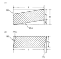
図4は、従来の弾性表面波素子片30と第1実施形態に係る弾性表面波素子片50との大きさを比較した図である。図4(1)は従来の弾性表面波素子片30であり、同図(2)は、第1実施形態の弾性表面波素子片50であって、斜線を施した部分がIDTおよび反射器を形成して素子片とするのに必要な領域を示している。従来の弾性表面波素子片30の面積Aは、弾性表面波素子片30の長さをL、幅をBとすると、
B1は、パワーフロー角をPFAとすると、
そこで、弾性表面波素子片30は、斜線で示した素子片を形成するのに必要とする最小面積に対する面積Aの比率rが、
ここで、斜線に示した必要とする領域からなる素子片(チップ)の寸法を、L=2mm、B0=0.5mmとすると、数式8は、
一方、図4(2)に示した実施形態の弾性表面波素子片50は、幅がB0である。しかし、長さがΔL=B0tan(PFA)だけ長くなる。したがって、実施形態に係る弾性表面波素子片50の面積Sは、
![]()
![]()
図5は、従来の弾性表面波素子片30を形成するためのフォトマスクと、第1実施形態の弾性表面波素子片50を形成するためのフォトマスクを模式的に示したものである。同図(1)が従来の弾性表面波素子片30を形成するためのフォトマスク70であり、(2)が実施形態に係る弾性表面波素子片50を形成するためのフォトマスク80であって、いずれもその一部を示している。
FIG. 5 schematically shows a conventional photomask for forming the surface acoustic
そして、フォトマスク70の斜線を施した部分は、スクライブライン71、72によって囲まれた1つの弾性表面波素子片30を形成する領域である。また、フォトマスク70の2点鎖線の領域74は、IDTと反射器とを形成するのに必要な領域を示しており、IDTと反射器とを形成するためのパターン(図示せず)が形成されている。領域74は、群速度の方向に沿ってIDTと反射器とを形成するために、図の横方向のスクライブライン71に対してパワーフロー角PFAだけ傾斜している。
The hatched portion of the
なお、フォトマスク70は、図示しない基準線を図7に示した水晶ウエハ90のオリエンテーションフラット92に合わせたときに、横方向のスクライブライン71がオリエンテーションフラット92に対して、面内回転角ψに等しい角度傾斜して配置される。すなわち、水晶ウエハ90は、STカット水晶基板であって、オリエンテーションフラット92が水晶のX軸に直交して形成してある。そして、水晶ウエハ90とフォトマスク70とを位置合わせする場合、フォトマスク70に形成した図示しない基準線を水晶ウエハ90のオリエンテーションフラット92に合わせるようになっている。したがって、フォトマスク70の横方向のスクライブライン71は、基準線に対して面内回転角ψに等しい角度傾斜する。
In the
一方、図5(2)に示したフォトマスク80は、斜線を施した部分が直交しているスクライブライン81、82によって囲まれた、1つの弾性表面波素子片50を形成する領域84である。そして、フォトマスク80は、図示しない基準線を水晶ウエハ90のオリエンテーションフラット92に合わせると、スクライブライン81が水晶ウエハ90のオリエンテーションフラット92に対して、面内回転角ψとパワーフロー角PFAとの和に等しい角度傾斜するように配置される。
On the other hand, the
図6は、実施の形態に係る弾性表面波素子片50の製造方法を説明するフローチャートである。弾性表面波素子片50を形成する場合、まずウエハ形成工程を行ない、水晶ウエハ90(図7参照)を作製する(図6のステップ100)。実施形態の場合、水晶ウエハ90は、オイラー角表示で(0°,113°〜135°,0°)のSTカット水晶基板からなっている。この水晶ウエハ90は、図7(1)に示したように、水晶ウエハ90の配置方向を示すとともに、フォトマスクなどとの位置合わせをするためのオリエンテーションフラット92が水晶のX軸に直交して形成してある。
FIG. 6 is a flowchart for explaining a method of manufacturing the surface acoustic
次に、図6のステップ102および図7(2)に示したように、水晶ウエハ90の表面に、アルミニウムなどの電極用の金属薄膜94を蒸着やスパッタリングなどによって成膜する成膜工程を行なう。その後、金属薄膜94の上にフォトレジストを塗布し、乾燥させてレジスト膜を形成するレジスト膜形成工程を行なう(ステップ104)。次に、図7(3)に示したフォトマスク80を水晶ウエハ90の上方に配置し、水晶ウエハ90の基準線であるオリエンテーションフラット92と、フォトマスク80の基準線(図示せず)とを合わせる露光位置決め工程を行なう(ステップ106)。フォトマスク80は、実施形態の場合、設けられているIDT形成用および反射器形成用のパターン86の配置方向が、基準線に対して、水晶ウエハ90を面内回転させる角度ψおよびパワーフロー角PFAに相当する角度傾斜させてある。したがって、フォトマスク80の基準線を水晶ウエハ90のオリエンテーションフラット92に合わせると、図5(2)に示したスクライブライン81および図7(3)に示したパターン86が、水晶ウエハ90の弾性表面波の群速度の方向に沿って配置される。
Next, as shown in
次に、フォトマスク80を介して水晶ウエハ90に設けたレジスト膜を露光し、さらに水晶ウエハ90を現像液に浸漬してレジスト膜を現像するフォト工程を行なう(ステップ108)。これにより、フォトマスク80に形成してあるIDT、反射器に対応したパターンがレジスト膜に転写される。その後、パターニングしたレジスト膜をマスクにして金属薄膜94をエッチングするパターニング工程を行なう(ステップ110、図7(4)参照)。そして、ステップ112に示したようにマスクにしたレジスト膜を除去する(ステップ112)。これにより、IDT34、反射器36などが形成される。その後、図7(5)に示したように分割工程を行なう。すなわち、ダイヤモンドソー96などによって、水晶ウエハ90をスクライブライン81、82に沿って切断、分割し、図7(6)に示したように、弾性表面波素子片50にする(ステップ114)。これにより、対向する二辺が弾性表面波の群速度の方向に沿った水晶板片からなる弾性表面波素子片50が得られる。
Next, the resist film provided on the
図8は、第2実施形態に係る弾性表面波素子片の平面図である。この実施形態に係る弾性表面波素子片50aは、水晶板片52の短辺64a、66aが反射器36を形成している導体ストリップ58と平行に形成してある。このため、水晶板片52は、四辺60、62、64a、66aがIDT34と反射器36とからなるパターン形状に沿って形成され、平行四辺形をなしている。このようになっている弾性表面波素子片50aは、水晶板片52の外形がIDT34、反射器36の外形に沿っているため、第1実施形態の弾性表面波素子片50よりも小さくすることができ、収率をより高めることができる。なお、弾性表面波素子片は、発振周波数がより高周波化されるのに伴って、水晶板片の端面の影響が小さくなってきている。したがって、辺64a、66aが弾性表面波の群速度の方向42と斜交していても、弾性表面波素子片50aのQ値に与える影響は小さい。このため、弾性表面波素子片を図9に示した第3実施形態のように形成してもよい。
FIG. 8 is a plan view of the surface acoustic wave element according to the second embodiment. In the surface acoustic
この第3実施形態の弾性表面波素子片50bは、反射器36のIDT34側と反対側が辺64a、66aの端縁まで延在して形成してある。このようになっている弾性表面波素子片50bは、長さをさらに短くすることができ、小型化が図れて水晶ウエハからの収率をさらに高めることができる。なお、辺64a、66aは、弾性表面波の位相速度の方向40と直交していてもよい。
The surface acoustic
上記の各実施形態に係る弾性表面波素子片50、50a、50bは、SAW共振子やSAWフィルタなどの弾性表面波装置に用いることができる。
The surface acoustic
34………IDT、36………反射器、40………位相速度の方向、42………群速度の方向、50、50a、50b………弾性表面波素子片、52………水晶板片、60、62、64、64a、66、66a………辺、PFA………パワーフロー角。 34 ......... IDT, 36 ......... Reflector, 40 ......... Direction of phase velocity, 42 ......... Direction of group velocity, 50, 50a, 50b ......... Surface acoustic wave element, 52 ......... Quartz Plate, 60, 62, 64, 64a, 66, 66a ......... side, PFA ......... power flow angle.
Claims (8)
前記水晶板片の表面に形成され、前記水晶板片の弾性表面波の位相速度の方向に対して、PFA±3°傾斜した方向に沿って配置されたすだれ状電極と反射器とを有し、
前記PFAが、
ことを特徴とする弾性表面波素子片。 An in-plane rotated ST-cut quartz plate piece having a cut angle of (0 °, 113 ° to 135 °, ± (40 ° to 49 °)) when the Euler angles are (φ °, θ °, ψ °);
A comb-like electrode formed on the surface of the quartz plate piece and disposed along a direction inclined by PFA ± 3 ° with respect to the direction of the phase velocity of the surface acoustic wave of the quartz plate piece, and a reflector ,
The PFA is
A surface acoustic wave element.
前記水晶板片は、対向する二辺が前記すだれ状電極と前記反射器との配置方向に沿っていることを特徴とする弾性表面波素子片。 The surface acoustic wave element piece according to claim 1,
2. The surface acoustic wave element piece according to claim 1, wherein two opposite sides of the quartz plate piece are along an arrangement direction of the interdigital electrode and the reflector.
前記水晶板片の対向する二辺は、前記群速度の方向に沿っている、
ことを特徴とする弾性表面波素子片。 Composed of a quartz plate piece in which interdigital electrodes are formed on the surface, the direction of the phase velocity of the surface acoustic wave is different from the direction of the group velocity,
Two opposite sides of the quartz plate piece are along the direction of the group velocity,
A surface acoustic wave element.
前記水晶板片は、四辺が前記すだれ状電極と前記反射器とからなるパターン形状に沿って形成されていることを特徴とする弾性表面波素子片。 In the surface acoustic wave element piece according to any one of claims 1 to 3,
The surface acoustic wave element piece, wherein the quartz plate piece is formed along a pattern shape having four sides of the interdigital electrode and the reflector.
前記水晶板片は、前記弾性表面波の群速度の方向と直交する二辺を有していることを特徴とする弾性表面波素子片。 In the surface acoustic wave element piece according to any one of claims 1 to 3,
The surface acoustic wave element piece, wherein the quartz plate piece has two sides orthogonal to the direction of the group velocity of the surface acoustic wave.
前記反射器は、前記すだれ状電極側と反対側が、前記水晶板片の端縁まで延在していることを特徴とする弾性表面波素子片。 In the surface acoustic wave element piece according to any one of claims 1 to 5,
The surface acoustic wave element piece, wherein the reflector has a side opposite to the interdigital electrode side extending to an edge of the quartz plate piece.
前記水晶ウエハの表面に金属薄膜を成膜する成膜工程と、
前記金属薄膜の上にレジスト膜を形成するレジスト膜形成工程と、
前記水晶ウエハの上方にフォトマスクを配置して両者の位置合わせを行ない、前記フォトマスクのIDT形成用および反射器形成用のパターンの配置方向を、前記水晶ウエハの弾性表面波の位相速度の方向とパワーフロー角異なった、予め求めた群速度の方向にする露光位置決め工程と、
前記レジスト膜を露光、現像するフォト工程と、
前記レジスト膜からなるマスクを用いて前記金属薄膜をエッチングしてIDTおよび反射器を形成するパターニング工程と、
前記水晶ウエハを切断し、対向する二辺が前記弾性表面波の群速度の方向に沿った素子片にする分割工程と、
を有することを特徴とする弾性表面波素子片の製造方法。 A wafer forming process for forming a quartz wafer having a predetermined cut angle;
A film forming step of forming a metal thin film on the surface of the quartz wafer;
A resist film forming step of forming a resist film on the metal thin film;
A photomask is arranged above the quartz wafer to align the two, and the arrangement direction of the pattern for forming the IDT and the reflector of the photomask is set to the phase velocity direction of the surface acoustic wave of the quartz wafer. And an exposure positioning step in which the power flow angle is different and the direction of the group velocity is obtained in advance.
A photo step of exposing and developing the resist film;
A patterning step of forming an IDT and a reflector by etching the metal thin film using a mask made of the resist film;
A dividing step of cutting the quartz wafer and making two opposing elements along the direction of the group velocity of the surface acoustic wave,
A method for producing a surface acoustic wave element, comprising:
Priority Applications (6)
| Application Number | Priority Date | Filing Date | Title |
|---|---|---|---|
| JP2004242806A JP2005204275A (en) | 2003-12-12 | 2004-08-23 | Surface acoustic wave element piece, its manufacturing method, and surface acoustic wave device |
| EP04029295A EP1542361A3 (en) | 2003-12-12 | 2004-12-10 | Surface acoustic wave element, method of manufacturing the same and surface acoustic wave device |
| DE602004025513T DE602004025513D1 (en) | 2003-12-12 | 2004-12-10 | Surface wave element and method for its production, and surface wave device |
| CNB2004101022540A CN100511995C (en) | 2003-12-12 | 2004-12-10 | Surface acoustic wave element piece and surface acoustic wave device |
| EP06015247A EP1720251B1 (en) | 2003-12-12 | 2004-12-10 | Surface acoustic wave element, method of manufacturing the same and surface acoustic wave device |
| US11/010,014 US7352104B2 (en) | 2003-12-12 | 2004-12-10 | Surface acoustic wave element, method of manufacturing the same and surface acoustic wave device |
Applications Claiming Priority (3)
| Application Number | Priority Date | Filing Date | Title |
|---|---|---|---|
| JP2003414210 | 2003-12-12 | ||
| JP2003423153 | 2003-12-19 | ||
| JP2004242806A JP2005204275A (en) | 2003-12-12 | 2004-08-23 | Surface acoustic wave element piece, its manufacturing method, and surface acoustic wave device |
Publications (1)
| Publication Number | Publication Date |
|---|---|
| JP2005204275A true JP2005204275A (en) | 2005-07-28 |
Family
ID=34527603
Family Applications (1)
| Application Number | Title | Priority Date | Filing Date |
|---|---|---|---|
| JP2004242806A Withdrawn JP2005204275A (en) | 2003-12-12 | 2004-08-23 | Surface acoustic wave element piece, its manufacturing method, and surface acoustic wave device |
Country Status (5)
| Country | Link |
|---|---|
| US (1) | US7352104B2 (en) |
| EP (2) | EP1720251B1 (en) |
| JP (1) | JP2005204275A (en) |
| CN (1) | CN100511995C (en) |
| DE (1) | DE602004025513D1 (en) |
Cited By (13)
| Publication number | Priority date | Publication date | Assignee | Title |
|---|---|---|---|---|
| US8063534B2 (en) | 2008-02-20 | 2011-11-22 | Seiko Epson Corporation | Surface acoustic wave device and surface acoustic wave oscillator |
| JP2012060418A (en) * | 2010-09-09 | 2012-03-22 | Seiko Epson Corp | Surface acoustic wave device, electronic apparatus and sensor device |
| JP2012060422A (en) * | 2010-09-09 | 2012-03-22 | Seiko Epson Corp | Surface acoustic wave device, electronic apparatus and sensor device |
| US8305162B2 (en) | 2009-02-27 | 2012-11-06 | Seiko Epson Corporation | Surface acoustic wave resonator and surface acoustic wave oscillator |
| US8476984B2 (en) | 2010-12-07 | 2013-07-02 | Seiko Epson Corporation | Vibration device, oscillator, and electronic apparatus |
| US8598766B2 (en) | 2010-12-03 | 2013-12-03 | Seiko Epson Corporation | Surface acoustic wave resonator, surface acoustic wave oscillator, and electronic apparatus |
| US8692439B2 (en) | 2010-08-26 | 2014-04-08 | Seiko Epson Corporation | Surface acoustic wave resonator, surface acoustic wave oscillator, and electronic device |
| US8723394B2 (en) | 2010-09-09 | 2014-05-13 | Seiko Epson Corporation | Surface acoustic wave device, electronic apparatus, and sensor apparatus |
| US8723396B2 (en) | 2010-09-09 | 2014-05-13 | Seiko Epson Corporation | Surface acoustic wave device, electronic apparatus, and sensor apparatus |
| US8928432B2 (en) | 2010-08-26 | 2015-01-06 | Seiko Epson Corporation | Surface acoustic wave resonator, surface acoustic wave oscillator, and electronic apparatus |
| US8933612B2 (en) | 2009-02-27 | 2015-01-13 | Seiko Epson Corporation | Surface acoustic wave resonator, surface acoustic wave oscillator, and electronic instrument |
| US9048806B2 (en) | 2010-09-09 | 2015-06-02 | Seiko Epson Corporation | Surface acoustic wave device, electronic apparatus, and sensor apparatus |
| US9088263B2 (en) | 2010-06-17 | 2015-07-21 | Seiko Epson Corporation | Surface acoustic wave resonator, surface acoustic wave oscillator, and electronic apparatus |
Families Citing this family (9)
| Publication number | Priority date | Publication date | Assignee | Title |
|---|---|---|---|---|
| DE102006048879B4 (en) | 2006-10-16 | 2018-02-01 | Snaptrack, Inc. | Electroacoustic component |
| FR2917918B1 (en) * | 2007-06-19 | 2010-03-12 | Senseor | SURFACE WAVE RESONATOR WITH REDUCED PARASITE RESONANCE |
| JP2011182220A (en) * | 2010-03-02 | 2011-09-15 | Panasonic Corp | Acoustic wave resonator and vertically coupled double mode filter using the same, as well as ladder filter |
| JP2012049817A (en) | 2010-08-26 | 2012-03-08 | Seiko Epson Corp | Surface acoustic wave device, surface acoustic wave oscillator, and electronic apparatus |
| DE102015106191A1 (en) * | 2015-04-22 | 2016-10-27 | Epcos Ag | Electro-acoustic component with improved acoustics |
| EP3106868A1 (en) * | 2015-06-15 | 2016-12-21 | Honeywell International Inc. | Acoustic wave based sensors |
| US11095266B2 (en) | 2016-10-07 | 2021-08-17 | Qorvo Us, Inc. | Slanted apodization for acoustic wave devices |
| DE102018130144A1 (en) * | 2018-11-28 | 2020-05-28 | RF360 Europe GmbH | Electroacoustic resonator and RF filter |
| CN112532205B (en) * | 2021-02-10 | 2021-05-25 | 成都频岢微电子有限公司 | Elastic surface wave resonator, filter and antenna sharing device |
Family Cites Families (8)
| Publication number | Priority date | Publication date | Assignee | Title |
|---|---|---|---|---|
| JPS5515887B2 (en) * | 1974-09-09 | 1980-04-26 | ||
| JPS5945286B2 (en) * | 1977-09-05 | 1984-11-05 | 松下電器産業株式会社 | Element for surface acoustic wave tip shaker |
| DE3230566A1 (en) * | 1982-08-17 | 1984-02-23 | Siemens AG, 1000 Berlin und 8000 München | ELECTRONIC COMPONENT WORKING WITH REFLECTED ACOUSTIC SHAFTS |
| CA1299732C (en) * | 1989-04-13 | 1992-04-28 | Bruce C. Beggs | Surface acoustic wave scattering grating |
| US5895996A (en) * | 1994-09-29 | 1999-04-20 | Seiko Epson Corporation | Saw device |
| FR2785473B1 (en) * | 1998-10-30 | 2001-01-26 | Thomson Csf | LOW LOSS FILTER WITH SURFACE ACOUSTIC WAVES ON OPTIMIZED QUARTZ SUBSTRATE |
| JP3724575B2 (en) * | 2001-08-09 | 2005-12-07 | セイコーエプソン株式会社 | Surface acoustic wave device |
| JP3622202B2 (en) * | 2001-08-29 | 2005-02-23 | セイコーエプソン株式会社 | Method for adjusting temperature characteristics of surface acoustic wave device |
-
2004
- 2004-08-23 JP JP2004242806A patent/JP2005204275A/en not_active Withdrawn
- 2004-12-10 CN CNB2004101022540A patent/CN100511995C/en not_active Expired - Fee Related
- 2004-12-10 DE DE602004025513T patent/DE602004025513D1/en active Active
- 2004-12-10 US US11/010,014 patent/US7352104B2/en not_active Expired - Fee Related
- 2004-12-10 EP EP06015247A patent/EP1720251B1/en not_active Expired - Fee Related
- 2004-12-10 EP EP04029295A patent/EP1542361A3/en not_active Withdrawn
Cited By (22)
| Publication number | Priority date | Publication date | Assignee | Title |
|---|---|---|---|---|
| US8063534B2 (en) | 2008-02-20 | 2011-11-22 | Seiko Epson Corporation | Surface acoustic wave device and surface acoustic wave oscillator |
| US8084918B2 (en) | 2008-02-20 | 2011-12-27 | Seiko Epson Corporation | Surface acoustic wave device and surface acoustic wave oscillator |
| US8237326B2 (en) | 2008-02-20 | 2012-08-07 | Seiko Epson Corporation | Surface acoustic wave device and surface acoustic wave oscillator |
| US9762207B2 (en) | 2009-02-27 | 2017-09-12 | Seiko Epson Corporation | Surface acoustic wave resonator, surface acoustic wave oscillator, and electronic instrument |
| US8305162B2 (en) | 2009-02-27 | 2012-11-06 | Seiko Epson Corporation | Surface acoustic wave resonator and surface acoustic wave oscillator |
| US8502625B2 (en) | 2009-02-27 | 2013-08-06 | Seiko Epson Corporation | Surface acoustic wave resonator and surface acoustic wave oscillator |
| US8952596B2 (en) | 2009-02-27 | 2015-02-10 | Seiko Epson Corporation | Surface acoustic wave resonator, surface acoustic wave oscillator, and electronic instrument |
| US8933612B2 (en) | 2009-02-27 | 2015-01-13 | Seiko Epson Corporation | Surface acoustic wave resonator, surface acoustic wave oscillator, and electronic instrument |
| US9537464B2 (en) | 2010-06-17 | 2017-01-03 | Seiko Epson Corporation | Surface acoustic wave resonator, surface acoustic wave oscillator, and electronic apparatus |
| US9088263B2 (en) | 2010-06-17 | 2015-07-21 | Seiko Epson Corporation | Surface acoustic wave resonator, surface acoustic wave oscillator, and electronic apparatus |
| US8928432B2 (en) | 2010-08-26 | 2015-01-06 | Seiko Epson Corporation | Surface acoustic wave resonator, surface acoustic wave oscillator, and electronic apparatus |
| US8692439B2 (en) | 2010-08-26 | 2014-04-08 | Seiko Epson Corporation | Surface acoustic wave resonator, surface acoustic wave oscillator, and electronic device |
| US8723395B2 (en) | 2010-09-09 | 2014-05-13 | Seiko Epson Corporation | Surface acoustic wave device, electronic apparatus, and sensor apparatus |
| US8723396B2 (en) | 2010-09-09 | 2014-05-13 | Seiko Epson Corporation | Surface acoustic wave device, electronic apparatus, and sensor apparatus |
| US8723393B2 (en) | 2010-09-09 | 2014-05-13 | Seiko Epson Corporation | Surface acoustic wave device, electronic apparatus, and sensor apparatus |
| US8723394B2 (en) | 2010-09-09 | 2014-05-13 | Seiko Epson Corporation | Surface acoustic wave device, electronic apparatus, and sensor apparatus |
| US9048806B2 (en) | 2010-09-09 | 2015-06-02 | Seiko Epson Corporation | Surface acoustic wave device, electronic apparatus, and sensor apparatus |
| JP2012060422A (en) * | 2010-09-09 | 2012-03-22 | Seiko Epson Corp | Surface acoustic wave device, electronic apparatus and sensor device |
| JP2012060418A (en) * | 2010-09-09 | 2012-03-22 | Seiko Epson Corp | Surface acoustic wave device, electronic apparatus and sensor device |
| US8791621B2 (en) | 2010-12-03 | 2014-07-29 | Seiko Epson Corporation | Surface acoustic wave resonator, surface acoustic wave oscillator, and electronic apparatus |
| US8598766B2 (en) | 2010-12-03 | 2013-12-03 | Seiko Epson Corporation | Surface acoustic wave resonator, surface acoustic wave oscillator, and electronic apparatus |
| US8476984B2 (en) | 2010-12-07 | 2013-07-02 | Seiko Epson Corporation | Vibration device, oscillator, and electronic apparatus |
Also Published As
| Publication number | Publication date |
|---|---|
| CN100511995C (en) | 2009-07-08 |
| EP1720251B1 (en) | 2010-02-10 |
| DE602004025513D1 (en) | 2010-03-25 |
| EP1720251A3 (en) | 2006-11-15 |
| EP1720251A2 (en) | 2006-11-08 |
| EP1542361A2 (en) | 2005-06-15 |
| CN1652461A (en) | 2005-08-10 |
| EP1542361A3 (en) | 2005-08-17 |
| US7352104B2 (en) | 2008-04-01 |
| US20050127781A1 (en) | 2005-06-16 |
Similar Documents
| Publication | Publication Date | Title |
|---|---|---|
| JP2005204275A (en) | Surface acoustic wave element piece, its manufacturing method, and surface acoustic wave device | |
| USRE47991E1 (en) | Acoustic wave element and acoustic wave device using same | |
| JP4569447B2 (en) | Surface acoustic wave element and surface acoustic wave device | |
| JP2010226636A (en) | Acoustic wave device and method of manufacturing the same | |
| JP2012124677A (en) | Vibrating device, oscillator and electronic apparatus | |
| JP2007028664A (en) | Surface acoustic wave element chip and surface acoustic wave device | |
| JP2006295311A (en) | Surface acoustic wave element chip and surface acoustic wave device | |
| JPH07263998A (en) | End face reflecting surface wave resonator | |
| JP2000188521A (en) | Surface acoustic wave device and two port surface acoustic wave resonator | |
| KR100427188B1 (en) | Surface acoustic wave device and method of producing the same | |
| JP2006074136A (en) | Surface acoustic wave element chip and surface acoustic wave device | |
| JP2007288812A5 (en) | ||
| JP2006186623A (en) | Surface acoustic wave element, manufacturing method thereof, and surface acoustic wave device | |
| JP2007036670A (en) | Manufacturing method of surface acoustic wave element, and the surface acoustic wave element | |
| KR0175201B1 (en) | Method for manufacturing surface wave devices of the end-face reflection type | |
| JP4174661B2 (en) | Surface acoustic wave device and manufacturing method thereof | |
| JP4557691B2 (en) | Surface acoustic wave device | |
| JP4706337B2 (en) | IDT design method for surface acoustic wave element, photomask for forming surface acoustic wave element, surface acoustic wave element manufacturing method, surface acoustic wave element | |
| JP2007053670A (en) | Elastic boundary wave element | |
| JP4756452B2 (en) | Photomask for forming surface acoustic wave element, method for manufacturing surface acoustic wave element, and surface acoustic wave element | |
| JP4868124B2 (en) | Surface acoustic wave resonator | |
| JPS6173409A (en) | Elastic surface wave device | |
| JP3909682B2 (en) | Photomask manufacturing method, photomask, and piezoelectric vibrating piece manufacturing method | |
| JP2009027671A (en) | Sh type bulk wave resonator | |
| JP2007228012A (en) | Surface acoustic wave resonator |
Legal Events
| Date | Code | Title | Description |
|---|---|---|---|
| A621 | Written request for application examination |
Free format text: JAPANESE INTERMEDIATE CODE: A621 Effective date: 20060620 |
|
| A977 | Report on retrieval |
Free format text: JAPANESE INTERMEDIATE CODE: A971007 Effective date: 20090202 |
|
| A131 | Notification of reasons for refusal |
Free format text: JAPANESE INTERMEDIATE CODE: A131 Effective date: 20090216 |
|
| A761 | Written withdrawal of application |
Free format text: JAPANESE INTERMEDIATE CODE: A761 Effective date: 20090408 |