JP3724575B2 - Surface acoustic wave device - Google Patents
Surface acoustic wave device Download PDFInfo
- Publication number
- JP3724575B2 JP3724575B2 JP2002152018A JP2002152018A JP3724575B2 JP 3724575 B2 JP3724575 B2 JP 3724575B2 JP 2002152018 A JP2002152018 A JP 2002152018A JP 2002152018 A JP2002152018 A JP 2002152018A JP 3724575 B2 JP3724575 B2 JP 3724575B2
- Authority
- JP
- Japan
- Prior art keywords
- surface acoustic
- acoustic wave
- quartz plate
- wave device
- cut quartz
- Prior art date
- Legal status (The legal status is an assumption and is not a legal conclusion. Google has not performed a legal analysis and makes no representation as to the accuracy of the status listed.)
- Expired - Fee Related
Links
Images


Classifications
-
- H—ELECTRICITY
- H03—ELECTRONIC CIRCUITRY
- H03H—IMPEDANCE NETWORKS, e.g. RESONANT CIRCUITS; RESONATORS
- H03H9/00—Networks comprising electromechanical or electro-acoustic devices; Electromechanical resonators
- H03H9/02—Details
- H03H9/02535—Details of surface acoustic wave devices
- H03H9/02543—Characteristics of substrate, e.g. cutting angles
- H03H9/02551—Characteristics of substrate, e.g. cutting angles of quartz substrates
Landscapes
- Physics & Mathematics (AREA)
- Acoustics & Sound (AREA)
- Surface Acoustic Wave Elements And Circuit Networks Thereof (AREA)
Abstract
Description
【0001】
【発明の属する技術分野】
本発明は、Z’軸まわりに面内回転させたSTカット水晶板(以下、面内回転STカット水晶板と称することがある)を用い、温度変化に対する周波数の変動を一層低減させるようにした弾性表面波装置に関する。
【0002】
【従来の技術】
従来、水晶片に代表される圧電体平板の主表面にIDT(Interdigital Transducer)電極を設けるとともに、このIDT電極の両端に複数の反射器を設け、高周波を安定して発振させる弾性表面波装置(以下、SAW共振子ということがある。)が知られている。
【0003】
そして前述したSAW共振子の中でも、温度変化に対する周波数の変動を低減させる目的から圧電体平板にSTカット水晶板を用い、当該STカット水晶板のX軸方向を弾性波の伝搬方向とした、STカットSAW共振子が知られている。
【0004】
図6は、STカットSAW共振子の構造を示す概略断面図である。
同図に示すように、STカットSAW共振子1は、STカット水晶板2を基板としており、基板主表面には、IDT電極3が設けられている。そしてIDT電極3においては、くし歯状の正極4と負極5とが交互に配置されており、これら正極4と負極5との間に高周波電界を加えることで、水晶板の圧電効果により弾性表面波が励振されるようになっている。
【0005】
また前記IDT電極3の両側には、弾性表面波を反射させる目的から、複数の反射器6が設けられており、当該反射器6に形成された複数の短絡電極7によって、IDT電極3から発せられた弾性表面波の反射を行うようにしている。なおIDT電極3における正極4と負極5、および反射器6における短絡電極7は、STカット水晶板2のX軸方向に沿って配列されるものであり、短絡電極7における弾性表面波の反射は、電極両縁部の位置で行われるようになっている。
【0006】
このように構成されたSTカットSAW共振子1において、図6に示すようにIDT電極3における正極4と負極5の幅とピッチをLt、Ptとし、反射器6における短絡電極7の幅とピッチをLr、Prと定義する。さらに正極4と負極5の膜厚をHt、および短絡電極7の膜厚をHrと定義する。
【0007】
図7は、STカットSAW共振子の短絡電極1本あたりの反射係数を示すグラフである。
STカットSAW共振子1においては、弾性表面波の反射係数を大きくすることができれば、反射器6の数を削減し、共振子自体を小型にすることが可能になる。そして同図においては、横軸にLt/Pt(=Lr/Pr、以下ηと称す)の値を示し、縦軸に短絡電極1本あたりの反射係数を示しており、前述のHt/2Pt(≒Hr/2Pr)の値によって反射係数がどの様に変動するかを示している。
【0008】
反射係数を考える場合、Ht/2PtとHr/2Prは、ほぼ同じ値と見なすことができ、2Pt≒2Prはλと定義される。このため本実施の形態においては、Ht/2PtとHr/2Prとを区別することなく、同一の値、すなわちH/λとして取り扱うものとする。
【0009】
図7に示すように、STカットSAW共振子1は、ηの値が大きくなるにつれて反射係数も大きくなることが知られており、さらにH/λと反射係数の関係についても、ηの値と同様、H/λの値が大きくなるほど反射係数が大きくなることが知られている(特開平2−260908号公報)。
【0010】
なおSTカットSAW共振子1では、正極4、負極5および短絡電極7の膜厚(H)は、目的とする温度特性を得る見地から、通常、H/λの値が0.03程度となるように設定される。一方ηの値は、Pt=2Ltの関係が成り立つよう0.5に設定される。
【0011】
ところでSAW共振子においては、温度変化による周波数変動を一層低減させる目的から、Z’軸まわりに面内回転させたSTカット水晶板から切り出した水晶振動板を用いる場合がある。しかしZ’軸まわりに面内回転させたSTカット水晶板では、ηならびにH/λの値と反射係数の関係などの検証がされていなかった。
【0012】
【発明が解決しようとする課題】
Z’軸まわりに面内回転させたSTカット水晶板は、発明者が検討したところ、従来のSTカット水晶板とは全く異なる特性を有しており、ηならびにH/λの値を大きくすることで反射係数を大きくするといった従来のSTカット水晶板の規則性が当てはまらないことが確認された。
このため、従来のSTカット水晶板の規則性をZ’軸まわりに面内回転させたSTカット水晶板に適用させて、ηならびにH/λの値を大きくしても反射係数が十分に得られないという問題が発生する。
【0013】
本発明は上記問題点に着目し、Z’軸まわりに面内回転させたSTカット水晶板の特性を把握することで、反射係数を大きくすることのできる弾性表面波装置を提供することを目的とする。
【0014】
【課題を解決するための手段】
本発明は、Z’軸まわりに面内回転させたSTカット水晶板の特性が、従来のSTカット水晶板の特性と異なるものであるという発明者の知見および種々の検討によって見いだされたものである。
【0015】
すなわち本発明に係る弾性表面波装置は、STカット水晶板をZ’軸回りに面内回転させたオイラー角が(0、113〜135、±(40〜49))にある面内回転STカット水晶板とし、その主表面上に、Rayleigh波を励振するための少なくとも一対のIDT電極を配置し、前記IDT電極のピッチPtと前記IDT電極の幅Ltの比率Lt/Ptが0.5未満であるものである。そして前記Lt/Ptが0.32±0.1であることが望ましく、さらに前記IDT電極の厚みをHtとし、Ht/2Ptが0.06±0.01であることが望ましい。
【0016】
また本発明に係る他の弾性表面波装置は、STカット水晶板をZ’軸回りに面内回転させたオイラー角が(0、113〜135、±(40〜49))にある面内回転STカット水晶板とし、その主表面上に、Rayleigh波を励振するための少なくとも一対のIDT電極と、前記Rayleigh波を閉じこめるための少なくとも一本の反射器とを配置し、前記IDT電極におけるピッチPtと前記IDT電極の幅Ltの比率Lt/Ptと、前記反射器におけるピッチPrと前記反射器の幅Lrの比率Lr/Prのうち、何れか一方または両方が0.5未満であるものである。
【0017】
なお前記Lt/Ptと、前記Lr/Prの何れか一方または両方が0.32±0.1であることが望ましく、さらに本発明に係る他の弾性表面波装置において前記IDT電極の厚みをHtとし、前記反射器の厚みをHrとし、Ht/2Ptと、Hr/2Prの何れか一方または両方が0.06±0.01であることが望ましい。
【0018】
このようにZ’軸まわりに面内回転させたSTカット水晶板を弾性表面波装置に適用すると、従来のSTカット水晶板を適用した弾性表面波装置と異なり、IDT電極におけるLt/Ptの値を小さくしていくと反射係数の数値が向上する。
【0019】
具体的には、Lt/Ptの値は、従来のSTカット水晶板を適用した弾性表面波装置に一般的に適用されるLt/Ptの値(0.5)より小さいことが望ましい。このようにLt/Ptの値を0.5未満に設定すれば、面内回転STカット水晶板を適用した弾性表面化装置の反射係数の数値を向上させることが可能となり、装置自体の小型化等を達成することができる。
【0020】
また上記作用に加え、IDT電極に隣接するよう設けられる反射器のLr/Prの値も、Lt/Ptと同様、0.5未満に設定すれば、反射係数の数値を向上させることが可能となり、装置自体の小型化等をさらに促進させることができる。なおLt/Ptの値、およびLr/Prの値を共に0.5未満に設定すれば反射係数の数値を一層向上させることができるが、Lt/Ptの値とLr/Prの値のいずれか一方を0.5未満に設定しても反射係数の数値の向上が図れることはいうまでもない。
【0021】
さらに発明者の検討によってLt/Ptと、Lr/Prの何れか一方または両方を0.32±0.1に設定したり、さらにHt/2Ptと、Hr/2Prの何れか一方または両方を0.06±0.01に設定したりすれば、より一層反射係数の数値が向上し、装置本体の小型化等を達成することができるのである。
【0022】
【発明の実施の形態】
以下に、本発明に係る弾性表面波装置に好適な具体的実施の形態を図面を参照して詳細に説明する。
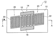
図1は、本実施の形態に係る弾性表面波装置の正面図であり、図2は、図1におけるAA略断面図である。
【0023】
これらの図に示すように、本実施の形態に係るSAW共振子となる弾性表面波装置10は、Z’軸まわりに面内回転させたSTカット水晶板12(以下、面内回転STカット水晶板12と称す)をベース基板として作製される。そして前記面内回転STカット水晶板12における表面の中央部分には、IDT電極14が設けられている。当該IDT電極14は、くし歯状からなる一対の正極側電極16と負極側電極18とからなり、これら両電極におけるくし歯を交互かつ平行に配置することで前記IDT電極14を構成するようにしている。このように圧電材料からなる面内回転STカット水晶板12の主表面に正極側電極16と負極側電極18を交互に配置し、これら両電極の間に高周波電界を加えることで、面内回転STカット水晶板12の圧電効果により弾性表面波が励振されるようになっている。
【0024】
また面内回転STカット水晶板12の主表面における、IDT電極14の両側には、複数の反射器20が設けられている。当該反射器20は、一定の幅を有した複数の短絡電極22を平行に配置した形態となっており、これら複数の短絡電極22によってIDT電極14にて発生した弾性表面波中のRayleigh波の反射を行うようにしている。
【0025】
ところでIDT電極14における正極側電極16と、負極側電極18、ならびに反射器20における短絡電極22は、面内回転STカット水晶板12におけるX’軸方向に沿って配列されるものであり、短絡電極22によるRayleigh波の反射は、電極の両縁部の位置で行われるようになっている。
【0026】
なお面内回転STカット水晶板12を用いた弾性表面波装置10において、図2に示すようにIDT電極14における正極側電極16と負極側電極18の幅と、ピッチをLt、Ptとし、一方反射器20における短絡電極22の幅と、ピッチをLr、Prとし、さらに正極側電極16と負極側電極18の膜厚をHt、および短絡電極22の膜厚をHrと定義する。
【0027】
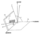
ここで弾性表面波装置10に使用される面内回転STカット水晶板12について説明する。図3は、Z’軸回りに面内回転させたSTカット水晶の説明図である。
同図に示すように、水晶の結晶軸は、電気軸(X軸)、機械軸(Y軸)、光軸(Z軸)によって定義されるが、STカットといわれるものはオイラー角(φ、θ、ψ)が(0、0、0)の水晶Z板24を、電気軸(X軸)周りにθ=113〜135度回転させて得られる水晶板26の新しい座標軸(X,Y’,Z’)に沿って切り出されるものである。このSTカット水晶板26のZ’軸周りにさらにψ=±(40〜49)度回転させ、弾性表面波の伝播方向がこのψにより定義されるX'軸の方向となるように作製された圧電基板がZ’軸回りに面内回転させた面内回転STカット水晶板12といわれるものである。この面内回転STカット水晶板12は、温度変化に対する周波数変化が極めて小さいことが知られている。
【0028】
そしてこのような面内回転STカット水晶板12を用いた弾性表面波装置10では、従来のSTカット水晶振動子を用いた弾性表面波装置とは、反射係数が異なることが発明者の検討によって見いだされた。
【0029】
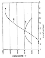
図4は、本実施の形態に係る弾性表面波装置と従来の弾性表面波装置との反射係数を比較したグラフである。同図においては、横軸にLt/Pt(=Lr/Pr、以下ηと称す)の値を示し、縦軸に短絡電極1本あたりの反射係数を示している。
【0030】
なお本実施の形態に係る弾性表面波装置の面内回転STカット水晶板の詳細は、θ=133度、ψ=43.4度で、H/λ=0.035に設定されている。一方、従来の弾性表面波装置のSTカット水晶板の詳細は、θ=133度、ψ=0度で、H/λ=0.03に設定されている。
【0031】
このように設定された本実施の形態に係る弾性表面波装置の特性を図中、第1ライン28により示し、従来の弾性表面波装置の特性を第2ライン30により示す。第2ライン30で示される従来装置の特性はηの値の増大に伴って反射係数の値が増大する傾向を示している。これに対し第1ライン28で示される本実施形態に係る装置では、前記第2ライン30に示されるような、ηの値の増大に伴って反射係数の値が増大するといった現象は確認されず、ηの値が0.3の近傍にあるときに反射係数の値が最大となり、ηがこの値よりも大きくても小さくても、反射係数の値は低下する特性となることが理解できる。
【0032】
また図5は、本実施の形態に係る弾性表面波装置において、H/λの変動に対する反射係数の関係を示したものであり、同図(1)は、計算結果を示す表を示し、同図(2)は、同図(1)における計算結果より作成したグラフである。この図5(1)に示すデータからηの値は、各H/λ値における最大反射係数となるη値の平均から最適値が0.32であることが求められる。さらに、高い共振周波数(高周波)を求められる弾性表面波装置においては電極がより微細化されるために、電極幅の製造バラツキの電極幅に対する相対的な誤差が大きくなる。現在の製造誤差は、例えば1GHz程度の発振周波数帯でのピッチPtは、音速を3,250m/secとすると、約1.625μm程度であるが、このときの電極幅の製造ばらつきは±0.16μm程度である。これをηに換算すると±0.1となる。
従って、面内回転STカット水晶版2のηが0.32±0.1の範囲にある時、反射係数は最大値をとるものであることが見出された。
【0033】
以上のことから、面内回転STカット水晶板12を用いた弾性表面波装置10においては、IDT電極14と反射器20、あるいはどちらか一方の電極の幅およびピッチを、ηの値が0.32±0.1の範囲内に収まるよう設定すれば、反射係数を向上させることができ、短絡電極22の電極数の低減が図れ、弾性表面波装置10の小型化等を図ることが可能になる。
【0034】
図4においては、面内回転STカット水晶板12を用いた弾性表面波装置10において、反射係数が最も高くなるηの範囲が有ることを説明したが、前記ηの値だけでなく、H/λの値を変動させることによっても反射係数を向上させることが図5に示されている。
【0035】
すなわち図5においては、本実施の形態に係る弾性表面波装置の面内回転STカット水晶板を、θ=123度、ψ=43度に設定し、H/λの値を0.02〜0.08の間で7段階に区切り、各H/λの値に対する反射係数の値を示したものであるが、同図(2)に示すように、H/λの値が0.06にあるときに反射係数の値が最大となり、H/λがこの値を外れた場合は、反射係数の値は低下することが判明する。
【0036】
さらに図5から、ηが0.2、0.3、0.4における反射係数の最大値を与えるH/λの値を計算し、その平均値をとってみてもH/λ=0.06において、反射係数は最大値をとることが判明した。
また、図5(2)からH/λが0.06±0.01を超える範囲では、反射係数の低下が大きく、このことからもH/λ=0.06±0.01が最適値であることが判る。
【0037】
従来のSTカット水晶板を用いた弾性表面波装置では、H/λの値が増大するのに伴い、反射係数の値も増大していくことが確認されているが、同図(2)のグラフに示すように、面内回転STカット水晶板を用いた弾性表面波装置の反射特性は、従来のSTカット水晶板を単に面内回転させただけにもかかわらず、その特性が従来のSTカット水晶板と著しく異なっていることが発明者の検討によって判明したのである。
【0038】
このように図5のグラフに示す結果から、面内回転STカット水晶板12を用いた弾性表面波装置10においては、IDT電極14と反射器20、あるいはどちらか一方の電極の厚みをH/λの値が0.06±0.01の範囲内に収まるよう設定すれば、反射係数を向上させることができ、短絡電極22等の電極数の低減が図れ、弾性表面波装置10の小型化等を図ることが可能になる。
そして上述したH/λの最適範囲に加え、前述した最も反射係数が高くなるηの値(0.32±0.1)に設計指針を一致させれば、一層反射係数を高めることができるのである。
【0039】
【発明の効果】
以上説明したように本発明によれば、STカット水晶板をZ’軸回りに面内回転させたオイラー角が(0、113〜135、±(40〜49))にある面内回転STカット水晶板とし、その主表面上に、Rayleigh波を励振するための少なくとも一対のIDT電極を配置し、前記IDT電極のピッチPtと前記IDT電極の幅Ltの比率Lt/Ptが0.5未満としたり、あるいはSTカット水晶板をZ’軸回りに面内回転させたオイラー角が(0、113〜135、±(40〜49))にある面内回転STカット水晶板とし、その主表面上に、Rayleigh波を励振するための少なくとも一対のIDT電極と、前記Rayleigh波を閉じこめるための少なくとも一本の反射器とを配置し、前記IDT電極におけるピッチPtと前記IDT電極の幅Ltの比率Lt/Ptと、前記反射器におけるピッチPrと前記反射器の幅Lrの比率Lr/Prのうち、何れか一方または両方が0.5未満としたことから、弾性表面波装置にZ’軸まわりに面内回転させたSTカット水晶板を用いた場合であってもRayleigh波の反射係数を大きくすることができ、これにより温度変化に対する周波数の変動を一層低減させるとともに、装置自体の小型化などを達成することが可能になる。
【図面の簡単な説明】
【図1】 本実施の形態に係る弾性表面波装置の正面図である。
【図2】 図1におけるAA略断面図である。
【図3】 Z’軸回りに面内回転させたSTカット水晶の説明図である。
【図4】 本実施の形態に係る弾性表面波装置と従来の弾性表面波装置との反射係数を比較したグラフである。
【図5】 本実施の形態に係る弾性表面波装置において、H/λの変動に対する反射係数の関係を示したものであり、同図(1)は、計算結果を示す表を示し、同図(2)は、同図(1)における計算結果より作成したグラフである。
【図6】 STカットSAW共振子の構造を示す略断面図である。
【図7】 STカットSAW共振子の短絡電極1本あたりの反射係数を示すグラフである。
【符号の説明】
1………STカットSAW共振子、2………STカット水晶板、3………IDT電極、4………正極、5………負極、6………反射器、7………短絡電極、10………弾性表面波装置、12………Z’軸まわりに面内回転させたSTカット水晶板、14………IDT電極、16………正極側電極、18………負極側電極、20………反射器、22………短絡電極、24………水晶Z板、26………水晶板、28………第1ライン、30………第2ライン[0001]
BACKGROUND OF THE INVENTION
The present invention uses an ST-cut quartz plate that is rotated in-plane around the Z ′ axis (hereinafter sometimes referred to as an in-plane rotated ST-cut quartz plate) and further reduces frequency fluctuations due to temperature changes. The present invention relates to a surface acoustic wave device.
[0002]
[Prior art]
Conventionally, an IDT (Interdigital Transducer) electrode is provided on the main surface of a piezoelectric flat plate represented by a quartz piece, and a plurality of reflectors are provided on both ends of the IDT electrode to stably oscillate a high frequency ( Hereinafter, it may be referred to as a SAW resonator).
[0003]
Among the SAW resonators described above, an ST cut quartz plate is used as the piezoelectric plate for the purpose of reducing frequency fluctuations with respect to temperature changes, and the ST axis of the ST cut quartz plate is defined as an elastic wave propagation direction. Cut SAW resonators are known.
[0004]
FIG. 6 is a schematic cross-sectional view showing the structure of the ST-cut SAW resonator.
As shown in the figure, the ST cut
[0005]
Further, a plurality of
[0006]
In the ST cut
[0007]
FIG. 7 is a graph showing the reflection coefficient per one short-circuit electrode of the ST cut SAW resonator.
In the ST-cut
[0008]
When considering the reflection coefficient, H t / 2P t and H r / 2P r can be regarded as substantially the same value, and 2P t ≈2P r is defined as λ. Therefore, in the present embodiment, H t / 2P t and H r / 2P r are treated as the same value, that is, H / λ, without being distinguished.
[0009]
As shown in FIG. 7, it is known that the ST-cut
[0010]
In the ST-cut
[0011]
By the way, in the SAW resonator, for the purpose of further reducing frequency fluctuation due to temperature change, there is a case where a crystal diaphragm cut out from an ST cut quartz plate rotated in-plane around the Z ′ axis is used. However, in the ST-cut quartz plate rotated in-plane around the Z ′ axis, the relationship between the values of η and H / λ and the reflection coefficient has not been verified.
[0012]
[Problems to be solved by the invention]
The ST-cut quartz plate rotated in-plane around the Z 'axis has characteristics that are completely different from those of the conventional ST-cut quartz plate as studied by the inventors, and increases the values of η and H / λ. Thus, it was confirmed that the regularity of the conventional ST-cut quartz plate that increases the reflection coefficient does not apply.
For this reason, the regularity of the conventional ST-cut quartz plate is applied to the ST-cut quartz plate rotated in-plane around the Z ′ axis, and a sufficient reflection coefficient can be obtained even if the values of η and H / λ are increased. The problem of not being able to occur.
[0013]
The present invention pays attention to the above-mentioned problems and aims to provide a surface acoustic wave device capable of increasing the reflection coefficient by grasping the characteristics of an ST-cut quartz plate rotated in-plane around the Z ′ axis. And
[0014]
[Means for Solving the Problems]
The present invention has been found by the inventors' knowledge and various studies that the characteristics of the ST-cut quartz plate rotated in-plane around the Z ′ axis are different from those of the conventional ST-cut quartz plate. is there.
[0015]
That is, the surface acoustic wave device according to the present invention has an in-plane rotation ST cut in which the Euler angles obtained by in-plane rotation of the ST cut quartz plate around the Z ′ axis are (0, 113 to 135, ± (40 to 49)). and quartz plate, the on the main surface, placing at least a pair of IDT electrodes for exciting a Rayleigh wave, the ratio L t / P t of width L t of the IDT electrode and the pitch P t of the IDT electrode is 0 those which are less than .5. The L t / P t is preferably 0.32 ± 0.1, the thickness of the IDT electrode is H t , and the H t / 2P t is preferably 0.06 ± 0.01. .
[0016]
In another surface acoustic wave device according to the present invention, an in-plane rotation with an Euler angle (0, 113 to 135, ± (40 to 49)) obtained by in-plane rotation of an ST cut quartz plate about the Z ′ axis is provided. An ST-cut quartz plate is disposed, and on its main surface, at least a pair of IDT electrodes for exciting a Rayleigh wave and at least one reflector for confining the Rayleigh wave are arranged, and a pitch P in the IDT electrode is arranged. the ratio L t / P t of width L t of t and the IDT electrode, of the ratio L r / P r of the width L r of the pitch P r and the reflector in the reflector, either one or both 0 those which are less than .5.
[0017]
In addition, it is desirable that one or both of the L t / P t and the L r / P r is 0.32 ± 0.1, and the IDT electrode in another surface acoustic wave device according to the present invention. It is desirable that the thickness of the reflector is H t , the thickness of the reflector is H r, and one or both of H t / 2P t and H r / 2P r is 0.06 ± 0.01.
[0018]
When the ST cut quartz plate rotated in-plane around the Z ′ axis in this way is applied to a surface acoustic wave device, unlike the conventional surface acoustic wave device using an ST cut quartz plate, L t / P t in the IDT electrode. As the value of is decreased, the numerical value of the reflection coefficient is improved.
[0019]
Specifically, the value of L t / P t is, is smaller than the value of is generally applied to the surface acoustic wave device using the conventional ST cut quartz crystal plate L t / P t (0.5) desirable. Thus, by setting the value of L t / P t to less than 0.5, it becomes possible to improve the numerical value of the reflection coefficient of the elastic surface forming device to which the in- plane rotating ST-cut quartz plate is applied, and the size of the device itself can be reduced. Can be achieved.
[0020]
In addition to the above action, if the value of L r / P r of the reflector provided adjacent to the IDT electrode is also set to less than 0.5, similarly to L t / P t , the numerical value of the reflection coefficient is improved. Therefore, it is possible to further promote downsizing of the device itself. Note that if both the value of L t / P t and the value of L r / P r are set to less than 0.5, the value of the reflection coefficient can be further improved, but the value of L t / P t and the value of L r Needless to say, even if one of the values of / Pr is set to less than 0.5, the value of the reflection coefficient can be improved.
[0021]
Further, as a result of the inventor's investigation, either or both of L t / P t and L r / P r are set to 0.32 ± 0.1, and H t / 2P t and H r / 2P r are set. If one or both of these are set to 0.06 ± 0.01, the numerical value of the reflection coefficient can be further improved, and the apparatus body can be downsized.
[0022]
DETAILED DESCRIPTION OF THE INVENTION
Hereinafter, specific embodiments suitable for a surface acoustic wave device according to the present invention will be described in detail with reference to the drawings.
FIG. 1 is a front view of a surface acoustic wave device according to the present embodiment, and FIG. 2 is a schematic cross-sectional view along AA in FIG.
[0023]
As shown in these drawings, the surface
[0024]
A plurality of
[0025]
By the way, the
[0026]
In the surface
[0027]
Here, the in-plane rotating ST cut
As shown in the figure, the crystal axis of quartz is defined by an electric axis (X axis), a mechanical axis (Y axis), and an optical axis (Z axis), but what is called ST cut is Euler angles (φ, A new coordinate axis (X, Y ′, .theta.) of the
[0028]
According to the inventors' investigation, the surface
[0029]
FIG. 4 is a graph comparing the reflection coefficients of the surface acoustic wave device according to the present embodiment and a conventional surface acoustic wave device. In the figure, the horizontal axis represents the value of L t / P t (= L r / P r , hereinafter referred to as η), and the vertical axis represents the reflection coefficient per one short-circuit electrode.
[0030]
The details of the in-plane rotating ST-cut quartz plate of the surface acoustic wave device according to the present embodiment are θ = 133 degrees, ψ = 43.4 degrees, and H / λ = 0.035. On the other hand, details of the ST cut quartz plate of the conventional surface acoustic wave device are set to θ = 133 degrees, ψ = 0 degrees, and H / λ = 0.03.
[0031]
The characteristics of the surface acoustic wave device according to the present embodiment set as described above are indicated by a
[0032]
FIG. 5 shows the relationship of the reflection coefficient to the fluctuation of H / λ in the surface acoustic wave device according to the present embodiment. FIG. 5A shows a table showing the calculation results. FIG. 2 is a graph created from the calculation result in FIG. From the data shown in FIG. 5 (1), the value of η is required to be an optimum value of 0.32 from the average of the η values that are the maximum reflection coefficients at the respective H / λ values. Furthermore, in a surface acoustic wave device that requires a high resonance frequency (high frequency), the electrodes are further miniaturized, so that a relative error with respect to the electrode width of the manufacturing variation of the electrode width increases. The current manufacturing error is, for example, the pitch P t in the oscillation frequency band of about 1 GHz is about 1.625 μm when the sound speed is 3,250 m / sec, but the manufacturing variation of the electrode width at this time is ± 0. .About 16 μm. When this is converted to η, it becomes ± 0.1.
Accordingly, it has been found that when the η of the in-plane rotated ST-cut
[0033]
From the above, in the surface
[0034]
In FIG. 4, it has been described that the surface
[0035]
That is, in FIG. 5, the in-plane rotating ST-cut quartz plate of the surface acoustic wave device according to the present embodiment is set to θ = 123 degrees and ψ = 43 degrees, and the value of H / λ is 0.02 to 0. .08 is divided into 7 stages, and the reflection coefficient value for each H / λ value is shown, but the H / λ value is 0.06 as shown in FIG. Sometimes, the value of the reflection coefficient becomes maximum, and when H / λ deviates from this value, it is found that the value of the reflection coefficient decreases.
[0036]
Further, from FIG. 5, the value of H / λ that gives the maximum value of the reflection coefficient when η is 0.2, 0.3, and 0.4 is calculated. It was found that the reflection coefficient had the maximum value.
Further, from FIG. 5 (2), in the range where H / λ exceeds 0.06 ± 0.01, the reduction of the reflection coefficient is large, and for this reason, H / λ = 0.06 ± 0.01 is the optimum value. I know that there is.
[0037]
In a surface acoustic wave device using a conventional ST-cut quartz plate, it has been confirmed that the value of the reflection coefficient increases as the value of H / λ increases. As shown in the graph, the reflection characteristics of the surface acoustic wave device using the in-plane rotated ST-cut quartz plate are the same as those obtained by simply rotating the conventional ST-cut quartz plate in-plane. It was found by the inventor's examination that it was significantly different from the cut quartz plate.
[0038]
Thus, from the results shown in the graph of FIG. 5, in the surface
In addition to the optimum range of H / λ described above, the reflection coefficient can be further increased if the design guideline is matched with the value of η (0.32 ± 0.1) at which the reflection coefficient is highest. is there.
[0039]
【The invention's effect】
As described above, according to the present invention, the in-plane rotation ST cut in which the Euler angles obtained by in-plane rotation of the ST cut quartz plate around the Z ′ axis are (0, 113 to 135, ± (40 to 49)). and quartz plate, the on the main surface, placing at least a pair of IDT electrodes for exciting a Rayleigh wave, the ratio L t / P t of width L t of the IDT electrode and the pitch P t of the IDT electrode is 0 or less than .5, or ST-cut quartz plate Z 'Euler angles plane rotated about the axis is set to (0,113~135, ± (40~49)) plane rotated ST cut quartz crystal plate in the thereof on the main surface, and at least one pair of IDT electrodes for exciting a Rayleigh wave, and at least one reflector for confining the Rayleigh wave arranged, the pitch P t in the IDT electrode The ratio L t / P t of width L t of DT electrodes, among the ratio L r / P r of the width L r of the pitch P r and the reflector in the reflector, one or both is less than 0.5 and since the can increase the reflection coefficient of the Rayleigh wave even in the case of using the ST-cut quartz plate plane rotated around axis Z 'in the surface acoustic wave device, thereby the frequency to the temperature change It is possible to further reduce the fluctuation of the apparatus and to achieve downsizing of the apparatus itself.
[Brief description of the drawings]
FIG. 1 is a front view of a surface acoustic wave device according to an embodiment.
FIG. 2 is a schematic cross-sectional view along AA in FIG.
FIG. 3 is an explanatory diagram of an ST cut crystal that is rotated in-plane around the Z ′ axis.
FIG. 4 is a graph comparing the reflection coefficients of the surface acoustic wave device according to the present embodiment and a conventional surface acoustic wave device.
FIG. 5 shows the relationship of the reflection coefficient with respect to the fluctuation of H / λ in the surface acoustic wave device according to the present embodiment. FIG. 5 (1) shows a table showing calculation results. (2) is a graph created from the calculation result in FIG.
FIG. 6 is a schematic cross-sectional view showing the structure of an ST cut SAW resonator.
FIG. 7 is a graph showing a reflection coefficient per one short-circuit electrode of an ST cut SAW resonator.
[Explanation of symbols]
1 ... ST cut SAW resonator, 2 ... ST cut quartz plate, 3 ......... IDT electrode, 4 ......... positive electrode, 5 ......... negative electrode, 6 ......... reflector, 7 ......... short circuit Electrode, 10... Surface acoustic wave device, 12... ST cut quartz plate rotated in-plane around Z ′ axis, 14... IDT electrode, 16. Side electrode, 20 ......... Reflector, 22 ......... Short-circuit electrode, 24 ......... Quartz Z plate, 26 ......... Quartz plate, 28 ......... First line, 30 ......... Second line
Claims (6)
Priority Applications (5)
| Application Number | Priority Date | Filing Date | Title |
|---|---|---|---|
| JP2002152018A JP3724575B2 (en) | 2001-08-09 | 2002-05-27 | Surface acoustic wave device |
| US10/211,578 US6774747B2 (en) | 2001-08-09 | 2002-08-05 | Surface acoustic wave device |
| DE60215597T DE60215597T2 (en) | 2001-08-09 | 2002-08-08 | Acoustic surface wave device |
| EP02017721A EP1289134B1 (en) | 2001-08-09 | 2002-08-08 | Surface acoustic wave device |
| AT02017721T ATE343869T1 (en) | 2001-08-09 | 2002-08-08 | SURFACE ACOUSTIC WAVE DEVICE |
Applications Claiming Priority (3)
| Application Number | Priority Date | Filing Date | Title |
|---|---|---|---|
| JP2001-242757 | 2001-08-09 | ||
| JP2001242757 | 2001-08-09 | ||
| JP2002152018A JP3724575B2 (en) | 2001-08-09 | 2002-05-27 | Surface acoustic wave device |
Publications (2)
| Publication Number | Publication Date |
|---|---|
| JP2003124780A JP2003124780A (en) | 2003-04-25 |
| JP3724575B2 true JP3724575B2 (en) | 2005-12-07 |
Family
ID=26620308
Family Applications (1)
| Application Number | Title | Priority Date | Filing Date |
|---|---|---|---|
| JP2002152018A Expired - Fee Related JP3724575B2 (en) | 2001-08-09 | 2002-05-27 | Surface acoustic wave device |
Country Status (5)
| Country | Link |
|---|---|
| US (1) | US6774747B2 (en) |
| EP (1) | EP1289134B1 (en) |
| JP (1) | JP3724575B2 (en) |
| AT (1) | ATE343869T1 (en) |
| DE (1) | DE60215597T2 (en) |
Families Citing this family (20)
| Publication number | Priority date | Publication date | Assignee | Title |
|---|---|---|---|---|
| JP3675373B2 (en) * | 2001-07-17 | 2005-07-27 | セイコーエプソン株式会社 | Method for adjusting temperature characteristics of oscillation circuit |
| JP2005204275A (en) * | 2003-12-12 | 2005-07-28 | Seiko Epson Corp | Surface acoustic wave element piece, its manufacturing method, and surface acoustic wave device |
| JP2006148622A (en) * | 2004-11-22 | 2006-06-08 | Seiko Epson Corp | Surface acoustic wave device and electronic equipment |
| JP4412292B2 (en) * | 2006-02-06 | 2010-02-10 | セイコーエプソン株式会社 | Surface acoustic wave device and electronic apparatus |
| JP4868124B2 (en) * | 2006-02-22 | 2012-02-01 | セイコーエプソン株式会社 | Surface acoustic wave resonator |
| JP4591800B2 (en) | 2008-02-20 | 2010-12-01 | エプソントヨコム株式会社 | Surface acoustic wave device and surface acoustic wave oscillator |
| EP2357729A4 (en) * | 2008-10-24 | 2015-03-25 | Seiko Epson Corp | Surface acoustic wave resonator, surface acoustic wave oscillator, and surface acoustic wave modular device |
| US8952596B2 (en) | 2009-02-27 | 2015-02-10 | Seiko Epson Corporation | Surface acoustic wave resonator, surface acoustic wave oscillator, and electronic instrument |
| JP4645923B2 (en) | 2009-02-27 | 2011-03-09 | セイコーエプソン株式会社 | Surface acoustic wave resonator and surface acoustic wave oscillator |
| JP2011182220A (en) * | 2010-03-02 | 2011-09-15 | Panasonic Corp | Acoustic wave resonator and vertically coupled double mode filter using the same, as well as ladder filter |
| JP5678486B2 (en) | 2010-06-17 | 2015-03-04 | セイコーエプソン株式会社 | Surface acoustic wave resonator, surface acoustic wave oscillator and electronic device |
| JP2012049817A (en) | 2010-08-26 | 2012-03-08 | Seiko Epson Corp | Surface acoustic wave device, surface acoustic wave oscillator, and electronic apparatus |
| JP2012049818A (en) | 2010-08-26 | 2012-03-08 | Seiko Epson Corp | Surface acoustic wave resonator, surface acoustic wave oscillator, and electronic apparatus |
| JP5934464B2 (en) | 2010-08-26 | 2016-06-15 | セイコーエプソン株式会社 | Surface acoustic wave resonator, surface acoustic wave oscillator, and electronic device |
| JP2012060420A (en) | 2010-09-09 | 2012-03-22 | Seiko Epson Corp | Surface acoustic wave device, electronic apparatus and sensor device |
| JP5652606B2 (en) | 2010-12-03 | 2015-01-14 | セイコーエプソン株式会社 | Surface acoustic wave resonator, surface acoustic wave oscillator, and electronic device |
| JP5648908B2 (en) | 2010-12-07 | 2015-01-07 | セイコーエプソン株式会社 | Vibration device, oscillator, and electronic device |
| EP2781022B1 (en) | 2011-11-17 | 2016-10-12 | Transense Technologies PLC | Resonant monolithic differential surface acoustic wave (saw) temperature sensing device |
| US10727741B2 (en) * | 2016-06-29 | 2020-07-28 | Win Semiconductors Corp. | Thermal sensing acoustic wave resonator and acoustic wave filter having thermal sensing acoustic wave resonator |
| US11095266B2 (en) * | 2016-10-07 | 2021-08-17 | Qorvo Us, Inc. | Slanted apodization for acoustic wave devices |
Family Cites Families (12)
| Publication number | Priority date | Publication date | Assignee | Title |
|---|---|---|---|---|
| US4232240A (en) * | 1979-05-31 | 1980-11-04 | The United States Of America As Represented By The Secretary Of The Air Force | High piezoelectric coupling X-cuts of lead potassium niobate, Pb2 Knb5 O15 , for surface acoustic wave applications |
| US4323809A (en) * | 1979-12-19 | 1982-04-06 | The United States Of America As Represented By The Secretary Of The Air Force | Surface acoustic wave substrate having orthogonal temperature compensated propagation directions and device applications |
| JPH02250413A (en) | 1989-03-23 | 1990-10-08 | Murata Mfg Co Ltd | Surface acoustic wave device |
| JPH02250412A (en) * | 1989-03-23 | 1990-10-08 | Murata Mfg Co Ltd | Surface acoustic wave device |
| JPH02260908A (en) | 1989-03-31 | 1990-10-23 | Murata Mfg Co Ltd | Surface acoustic wave device |
| US5081389A (en) * | 1990-11-30 | 1992-01-14 | Ascom Zelcom Ag. | Crystal cut angles for lithium tantalate crystal for novel surface acoustic wave devices |
| WO1996010293A1 (en) * | 1994-09-29 | 1996-04-04 | Seiko Epson Corporation | Saw device |
| DE69608997T2 (en) | 1995-04-12 | 2000-11-16 | Matsushita Electric Ind Co Ltd | Resonator chain filter with surface acoustic waves |
| WO1997012398A1 (en) * | 1995-09-29 | 1997-04-03 | Analog Devices, Inc. | Integrated circuit and supply decoupling capacitor therefor |
| JPH11136083A (en) * | 1997-08-27 | 1999-05-21 | Murata Mfg Co Ltd | Surface wave device |
| JP3414371B2 (en) * | 2000-07-31 | 2003-06-09 | 株式会社村田製作所 | Surface acoustic wave device and method of manufacturing the same |
| JP2002176333A (en) * | 2000-12-07 | 2002-06-21 | Fujitsu Media Device Kk | Surface acoustic wave filter |
-
2002
- 2002-05-27 JP JP2002152018A patent/JP3724575B2/en not_active Expired - Fee Related
- 2002-08-05 US US10/211,578 patent/US6774747B2/en not_active Expired - Lifetime
- 2002-08-08 EP EP02017721A patent/EP1289134B1/en not_active Expired - Lifetime
- 2002-08-08 AT AT02017721T patent/ATE343869T1/en not_active IP Right Cessation
- 2002-08-08 DE DE60215597T patent/DE60215597T2/en not_active Expired - Lifetime
Also Published As
| Publication number | Publication date |
|---|---|
| EP1289134B1 (en) | 2006-10-25 |
| DE60215597T2 (en) | 2007-08-23 |
| DE60215597D1 (en) | 2006-12-07 |
| EP1289134A3 (en) | 2004-02-25 |
| JP2003124780A (en) | 2003-04-25 |
| US6774747B2 (en) | 2004-08-10 |
| EP1289134A2 (en) | 2003-03-05 |
| ATE343869T1 (en) | 2006-11-15 |
| US20030030513A1 (en) | 2003-02-13 |
Similar Documents
| Publication | Publication Date | Title |
|---|---|---|
| JP3724575B2 (en) | Surface acoustic wave device | |
| JP4591800B2 (en) | Surface acoustic wave device and surface acoustic wave oscillator | |
| US7696675B2 (en) | Surface acoustic wave device and electronic apparatus | |
| JP3622202B2 (en) | Method for adjusting temperature characteristics of surface acoustic wave device | |
| US8502625B2 (en) | Surface acoustic wave resonator and surface acoustic wave oscillator | |
| US7042133B2 (en) | Surface acoustic wave device and method of adjusting a temperature characteristic of the same | |
| JPWO2018097016A1 (en) | Elastic wave device | |
| JP2010088141A (en) | Surface acoustic wave device and surface acoustic wave oscillator | |
| US6556104B2 (en) | Surface acoustic wave devices using optimized cuts of a piezoelectric substrate | |
| JP4059152B2 (en) | Surface acoustic wave resonator | |
| JPH0134411B2 (en) | ||
| JP2000188521A (en) | Surface acoustic wave device and two port surface acoustic wave resonator | |
| JPS632414A (en) | Elastic surface wave resonator | |
| JPS63135010A (en) | Surface acoustic wave resonator | |
| US8471434B2 (en) | Surface acoustic wave device, surface acoustic wave oscillator, and electronic apparatus | |
| US6160339A (en) | Two-port saw resonator | |
| JPH02295212A (en) | Surface acoustic wave resonator | |
| JPS63194406A (en) | Surface acoustic wave resonator | |
| WO2024029361A1 (en) | Elastic wave device and filter device | |
| JP2012105252A (en) | Surface acoustic wave device | |
| WO2024117050A1 (en) | Elastic wave device and filter device | |
| JP2002223143A (en) | Surface acoustic wave device | |
| JPH02250413A (en) | Surface acoustic wave device | |
| JP2005184340A (en) | Surface acoustic wave chip | |
| JP2001358555A (en) | Surface acoustic wave resonator |
Legal Events
| Date | Code | Title | Description |
|---|---|---|---|
| A871 | Explanation of circumstances concerning accelerated examination |
Free format text: JAPANESE INTERMEDIATE CODE: A871 Effective date: 20040524 |
|
| A975 | Report on accelerated examination |
Free format text: JAPANESE INTERMEDIATE CODE: A971005 Effective date: 20040528 |
|
| A131 | Notification of reasons for refusal |
Free format text: JAPANESE INTERMEDIATE CODE: A131 Effective date: 20040916 |
|
| A521 | Request for written amendment filed |
Free format text: JAPANESE INTERMEDIATE CODE: A523 Effective date: 20041111 |
|
| TRDD | Decision of grant or rejection written | ||
| A01 | Written decision to grant a patent or to grant a registration (utility model) |
Free format text: JAPANESE INTERMEDIATE CODE: A01 Effective date: 20050831 |
|
| A61 | First payment of annual fees (during grant procedure) |
Free format text: JAPANESE INTERMEDIATE CODE: A61 Effective date: 20050913 |
|
| R150 | Certificate of patent or registration of utility model |
Free format text: JAPANESE INTERMEDIATE CODE: R150 |
|
| FPAY | Renewal fee payment (event date is renewal date of database) |
Free format text: PAYMENT UNTIL: 20080930 Year of fee payment: 3 |
|
| FPAY | Renewal fee payment (event date is renewal date of database) |
Free format text: PAYMENT UNTIL: 20090930 Year of fee payment: 4 |
|
| FPAY | Renewal fee payment (event date is renewal date of database) |
Free format text: PAYMENT UNTIL: 20090930 Year of fee payment: 4 |
|
| FPAY | Renewal fee payment (event date is renewal date of database) |
Free format text: PAYMENT UNTIL: 20100930 Year of fee payment: 5 |
|
| FPAY | Renewal fee payment (event date is renewal date of database) |
Free format text: PAYMENT UNTIL: 20100930 Year of fee payment: 5 |
|
| FPAY | Renewal fee payment (event date is renewal date of database) |
Free format text: PAYMENT UNTIL: 20110930 Year of fee payment: 6 |
|
| FPAY | Renewal fee payment (event date is renewal date of database) |
Free format text: PAYMENT UNTIL: 20120930 Year of fee payment: 7 |
|
| FPAY | Renewal fee payment (event date is renewal date of database) |
Free format text: PAYMENT UNTIL: 20130930 Year of fee payment: 8 |
|
| S531 | Written request for registration of change of domicile |
Free format text: JAPANESE INTERMEDIATE CODE: R313531 |
|
| R350 | Written notification of registration of transfer |
Free format text: JAPANESE INTERMEDIATE CODE: R350 |
|
| LAPS | Cancellation because of no payment of annual fees |