JP2012060418A - Surface acoustic wave device, electronic apparatus and sensor device - Google Patents
Surface acoustic wave device, electronic apparatus and sensor device Download PDFInfo
- Publication number
- JP2012060418A JP2012060418A JP2010201749A JP2010201749A JP2012060418A JP 2012060418 A JP2012060418 A JP 2012060418A JP 2010201749 A JP2010201749 A JP 2010201749A JP 2010201749 A JP2010201749 A JP 2010201749A JP 2012060418 A JP2012060418 A JP 2012060418A
- Authority
- JP
- Japan
- Prior art keywords
- idt
- saw
- angle
- electrode
- acoustic wave
- Prior art date
- Legal status (The legal status is an assumption and is not a legal conclusion. Google has not performed a legal analysis and makes no representation as to the accuracy of the status listed.)
- Pending
Links
Images


Classifications
-
- H—ELECTRICITY
- H03—ELECTRONIC CIRCUITRY
- H03H—IMPEDANCE NETWORKS, e.g. RESONANT CIRCUITS; RESONATORS
- H03H9/00—Networks comprising electromechanical or electro-acoustic devices; Electromechanical resonators
- H03H9/02—Details
- H03H9/02535—Details of surface acoustic wave devices
- H03H9/02543—Characteristics of substrate, e.g. cutting angles
- H03H9/02551—Characteristics of substrate, e.g. cutting angles of quartz substrates
-
- H—ELECTRICITY
- H03—ELECTRONIC CIRCUITRY
- H03H—IMPEDANCE NETWORKS, e.g. RESONANT CIRCUITS; RESONATORS
- H03H9/00—Networks comprising electromechanical or electro-acoustic devices; Electromechanical resonators
- H03H9/02—Details
- H03H9/05—Holders; Supports
- H03H9/0538—Constructional combinations of supports or holders with electromechanical or other electronic elements
- H03H9/0542—Constructional combinations of supports or holders with electromechanical or other electronic elements consisting of a lateral arrangement
-
- H—ELECTRICITY
- H03—ELECTRONIC CIRCUITRY
- H03H—IMPEDANCE NETWORKS, e.g. RESONANT CIRCUITS; RESONATORS
- H03H9/00—Networks comprising electromechanical or electro-acoustic devices; Electromechanical resonators
- H03H9/02—Details
- H03H9/125—Driving means, e.g. electrodes, coils
- H03H9/145—Driving means, e.g. electrodes, coils for networks using surface acoustic waves
- H03H9/14544—Transducers of particular shape or position
- H03H9/14594—Plan-rotated or plan-tilted transducers
Landscapes
- Physics & Mathematics (AREA)
- Acoustics & Sound (AREA)
- Surface Acoustic Wave Elements And Circuit Networks Thereof (AREA)
- Oscillators With Electromechanical Resonators (AREA)
Abstract
Description
本発明は、弾性表面波(surface acoustic wave:SAW)を利用した共振子、発振器等の弾性表面波デバイス、SAWデバイスを備えた電子機器及びセンサー装置に関する。 The present invention relates to a surface acoustic wave device such as a resonator and an oscillator using a surface acoustic wave (SAW), an electronic apparatus including the SAW device, and a sensor device.
SAWデバイスは、例えば携帯電話、ハードディスク、パーソナルコンピューター、BS及びCS放送の受信チューナー、同軸ケーブルまたは光ケーブル中を伝播する高周波信号や光信号の処理機器、広い温度範囲で高周波・高精度クロック(低ジッタ、低位相雑音)を必要とするサーバー・ネットワーク機器、無線通信用機器等の電子機器や、圧力センサー、加速度センサー、回転速度センサー等の各種センサー装置に広く利用されている。これらの機器・装置は、特に最近の情報通信の高速化によるリファレンスクロックの高周波化や装置筐体の小型化に伴い、装置内部での発熱の影響が大きくなっている。そのため、装置内部に搭載される電子デバイスは、動作温度範囲の拡大や高精度化が要求され、例えば屋外に設置される無線基地局のように低温から高温まで温度変化の激しい環境下で長期に亘って安定した動作が必要となっている。 SAW devices include, for example, mobile phones, hard disks, personal computers, BS and CS broadcast reception tuners, coaxial cables or optical signal processing equipment that propagates in optical cables, and high-frequency, high-precision clocks (low jitter over a wide temperature range). , Low phase noise) is widely used in electronic devices such as server / network equipment, wireless communication equipment, and various sensor devices such as pressure sensors, acceleration sensors, and rotational speed sensors. In these devices and apparatuses, the influence of heat generation inside the apparatus is increasing with the recent increase in the frequency of the reference clock and the downsizing of the apparatus housing due to the speeding up of information communication. For this reason, electronic devices mounted inside the device are required to have a wide operating temperature range and high accuracy.For example, wireless base stations installed outdoors can be used for long periods of time in environments where temperature changes from low to high. Therefore, stable operation is required.
一般にSAW共振子等のSAWデバイスにおいて、周波数温度特性の変化には、SAWのストップバンドや使用する水晶基板のカット角、基板上に形成されるIDT(interdigital transducer:すだれ状トランスデューサ)の形態等が大きい影響を及ぼす。例えば、SAWの1波長当たり3本の電極指で構成される単位区間を圧電基板上に繰り返し配列したIDTを有し、SAWのストップバンドの上端モード、下端モードのそれぞれを励起させる反射反転型SAW変換器が提案されている(例えば、特許文献1を参照)。この反射反転型SAW変換器によりSAWフィルタを構成すれば、通過帯域近傍の高域側阻止域において高減衰量が実現できるとされている。 In general, in a SAW device such as a SAW resonator, changes in frequency temperature characteristics include the SAW stop band, the cut angle of the quartz substrate used, and the form of the IDT (interdigital transducer) formed on the substrate. It has a big impact. For example, a reflection inversion SAW having an IDT in which unit sections composed of three electrode fingers per wavelength of SAW are repeatedly arranged on a piezoelectric substrate, and exciting each of the upper end mode and the lower end mode of the SAW stop band. A converter has been proposed (see, for example, Patent Document 1). If a SAW filter is constituted by this reflection inversion type SAW converter, it is said that a high attenuation can be realized in the high band side stop band near the pass band.
また、オイラー角(φ,θ,ψ)=(0°、123°、0°)の所謂STカット水晶基板を用いた反射反転型SAW変換器が知られている(例えば、特許文献2を参照)。同特許文献には、ストップバンドの上端の共振を励振させることができ、ストップバンドの下端の共振を用いる場合よりも周波数温度特性が向上すると記載されている。更に、SAWにおけるストップバンドの上端モードの方が、ストップバンドの下端モードよりも周波数温度特性が良好であると報告されている(例えば、特許文献3〜6を参照)。
Further, a reflection inversion SAW converter using a so-called ST-cut quartz substrate with Euler angles (φ, θ, ψ) = (0 °, 123 °, 0 °) is known (see, for example, Patent Document 2). ). The patent document describes that the resonance at the upper end of the stop band can be excited and the frequency temperature characteristic is improved as compared with the case of using the resonance at the lower end of the stop band. Furthermore, it has been reported that the upper end mode of the stop band in SAW has better frequency temperature characteristics than the lower end mode of the stop band (see, for example,
特に特許文献3、4には、レイリー波を利用したSAW装置において良好な周波数温度特性を得るために、水晶基板のカット角を調整すると共に、IDT電極の基準化膜厚(H/λ)を0.1程度まで厚くすることが記載されている。特許文献3に記載のSAW共振子は、オイラー角(φ,θ,ψ)=(φ=0°、0°≦θ≦180°、0°<|ψ|<90°)の水晶基板上に、SAWの1波長当たり2本の電極指で構成される単位区間を繰り返し配列したシングル型IDT電極を有する。これにより、レイリー波をストップバンドの上限モードで励振させ、それを利用してSAW共振子の高周波化と良好な周波数温度特性を実現することができる。
In particular, in
特許文献4には、前記シングル型IDT電極を有するSAW装置において、水晶基板をオイラー角(φ,θ,ψ)=(φ=0°、110°≦θ≦140°、38°≦|ψ|≦44°)に設定し、IDT電極の厚みH、IDT電極における電極指の幅d、IDT電極における電極指間のピッチP、及びSAWの波長λにより規定される基準化電極膜厚(H/λ)と基準化電極幅η(=d/P)との関係を、
H/λ≧0.1796η3−0.4303η2+0.2071η+0.0682
に設定することが開示されている。これによって、レイリー波をストップバンドの上限モードで励振させ、良好な周波数温度特性を実現することができる。
In
H / λ ≧ 0.1796η 3 −0.4303η 2 + 0.2071η + 0.0682
Is disclosed. As a result, Rayleigh waves can be excited in the upper limit mode of the stop band, and good frequency temperature characteristics can be realized.
特許文献5には、オイラー角(φ,θ,ψ)=(0°,θ,9°<|ψ|<46°)、好ましくは(0°,95°<θ<155°,33°<|ψ|<46°)の水晶基板上にシングル型IDT電極を配置し、基準化電極膜厚(H/λ)を0.045≦H/λ≦0.085としたSAW素子が開示されている。これによって、レイリー波をストップバンドの上限モードで励振させ、良好な周波数温度特性を実現することができる。
In
特許文献6には、オイラー角(φ,θ,ψ)=(0°123°,43.2°)の面内回転STカット水晶基板上に前記シングル型IDT電極を配置し、その基準化電極膜厚(H/λ)をH/λ=0.06、所謂6%λとすることによって、レイリー波をストップバンドの上限モードで励振させるSAW素子が開示されている。更にこのSAW素子は、IDT電極の電極指幅Ltと電極指ピッチPtとにより規定される標準化電極幅η(=Lt/Pt)を、0.5≦η≦0.7に設定することによって、常温(25℃)において最大830ppmの周波数偏差を実現することができる。
In
他方、IDTを構成する電極指間及び反射器を構成する導体ストリップ間の水晶基板表面にグルーブ即ち溝を形成したSAW共振器が知られている(例えば、特許文献7及び非特許文献1を参照)。特許文献7には、STカットX伝搬水晶基板にIDT及び反射器のアルミ電極で構成し、かつ水晶基板表面のIDTを構成する電極指間及び反射器を構成する導体ストリップ間に露出した領域に溝を形成することにより、Q値が高く容量比が低くなり、共振抵抗の低いSAW共振器を実現できることが開示されている。更に同特許文献には、IDTの溝と反射器の溝とを同じ深さにした構造、及び反射器の溝をIDTの溝より深くした構造が記載されている。 On the other hand, a SAW resonator is known in which grooves or grooves are formed on the surface of a quartz substrate between electrode fingers constituting an IDT and between conductor strips constituting a reflector (see, for example, Patent Document 7 and Non-Patent Document 1). ). In Patent Document 7, the ST cut X propagation quartz substrate is composed of an IDT and an aluminum electrode of a reflector, and is exposed between the electrode fingers constituting the IDT on the quartz substrate surface and between the conductor strips constituting the reflector. It is disclosed that a SAW resonator having a high Q value and a low capacitance ratio and a low resonance resistance can be realized by forming a groove. Furthermore, the patent document describes a structure in which the groove of the IDT and the groove of the reflector are made the same depth, and a structure in which the groove of the reflector is deeper than the groove of the IDT.
非特許文献1には、STカット水晶基板を用いたグループ型SAW共振器の特性が記載されている。その周波数温度特性は、SAW伝搬基板の電極で覆われていない水晶面に形成した溝の深さにより変化すること、及び、溝が深くなるに従って、上向き凸の2次曲線の頂点温度Tpが低くなっていくことが報告されている。
Non-Patent
このように水晶等の圧電基板に溝を形成して実効膜厚を調整することによって周波数を調整する方法は、当業者によく知られている(例えば、特許文献8乃至11を参照)。特許文献8記載のSAWデバイスは、IDTを形成した圧電基板の表面を、該圧電基板のエッチングレートがIDTのエッチングレートより大きくなる条件でエッチングし、その周波数を下降させるように微調整する。特許文献9乃至11においても、同様に圧電基板の表面をその上に形成したIDTをマスクとしてドライエッチングすることにより、SAWデバイスの周波数を低域側へシフトさせている。
A method of adjusting the frequency by adjusting the effective film thickness by forming a groove in a piezoelectric substrate such as quartz is well known to those skilled in the art (see, for example,
更に、トランスバーサル型SAWフィルタにおいて、IDT電極の電極指間の圧電基板表面をエッチング加工して溝を形成することにより見かけ上伝搬速度を小さくすることが知られている(例えば、特許文献12を参照)。これによって、SAWフィルタの基本設計を変更せずに、IDT電極の電極指ピッチを小さくでき、チップの小型化を実現することができる。 Furthermore, in a transversal SAW filter, it is known that the propagation speed is apparently reduced by etching a piezoelectric substrate surface between electrode fingers of an IDT electrode to form a groove (for example, see Patent Document 12). reference). As a result, the electrode finger pitch of the IDT electrode can be reduced without changing the basic design of the SAW filter, and the chip can be downsized.
また、SSBW(Surface Skimming Bulk Wave)と呼ばれるすべり波を励振するSAW共振器において、回転Yカット、カットアングル−43°乃至−52°、すべり波伝搬方向をZ’軸方向(オイラー角(φ,θ,ψ)=(0°,38≦θ≦47,90°))の水晶基板に、基準化電極膜厚(H/λ)が2.0≦H/λ≦4.0%のIDT電極をアルミで形成することにより、三次曲線の周波数温度特性を実現し得ることが知られている(例えば、特許文献13を参照)。すべり波(SH波)はその振動エネルギーを電極直下に閉じ込めて圧電基板の表面直下を伝搬するので、SAWが基板表面に沿って伝搬するSTカット水晶SAWデバイスと比較して、反射器によるSAWの反射効率が悪く、小型化及び高いQ値を実現し難いという問題がある。 Further, in a SAW resonator that excites a slip wave called SSBW (Surface Skimming Bulk Wave), the rotation Y-cut, the cut angle of −43 ° to −52 °, and the slip wave propagation direction in the Z′-axis direction (Eulerian angle (φ, θT, ψ) = (0 °, 38 ≦ θ ≦ 47, 90 °)) and an IDT electrode having a normalized electrode film thickness (H / λ) of 2.0 ≦ H / λ ≦ 4.0% It is known that the frequency temperature characteristic of a cubic curve can be realized by forming aluminum with aluminum (see, for example, Patent Document 13). A slip wave (SH wave) confines its vibration energy directly under the electrode and propagates directly under the surface of the piezoelectric substrate. Therefore, compared with an ST-cut quartz SAW device in which SAW propagates along the substrate surface, There is a problem in that the reflection efficiency is poor and it is difficult to achieve miniaturization and a high Q value.
この問題を解決するために、オイラー角(φ,θ,ψ)=(0°,−64°<θ<−49.3°,85°≦ψ≦95°)の回転Yカット水晶基板の表面にIDTとグレーティング反射器とを形成し、SH波を励振するSAWデバイスが提案されている(例えば、特許文献14を参照)。このSAWデバイスは、SAWの波長λで基準化される電極膜厚H/λを0.04<H/λ<0.12に設定することによって、小型化、高いQ値及び優れた周波数安定性を実現している。 In order to solve this problem, the surface of a rotated Y-cut quartz substrate with Euler angles (φ, θ, ψ) = (0 °, −64 ° <θ <−49.3 °, 85 ° ≦ ψ ≦ 95 °) A SAW device that forms an IDT and a grating reflector and excites SH waves has been proposed (for example, see Patent Document 14). This SAW device is small in size, high Q value and excellent frequency stability by setting the electrode film thickness H / λ normalized by the SAW wavelength λ to 0.04 <H / λ <0.12. Is realized.
更に、かかるSAWデバイスにおいて、電極膜厚が厚いことに起因して発生するストレスマイグレーションが原因となってQ値や周波数安定性が劣化するという問題を解決するために、IDTの電極指間の水晶基板に溝を形成することが提案されている(例えば、特許文献15を参照)。この溝の深さをHp、IDTの金属膜の膜厚をHmとしたとき、SAWの波長λで基準化した電極膜厚H/λを0.04<H/λ<0.12(ただし、H=Hp+Hm)の範囲と設定することにより、金属膜の見掛け上の膜厚を薄くできるので、通電時のストレスマイグレーションによる周波数変動を抑圧し、Q値が高く、周波数安定性の優れたSAWデバイスを実現できる。 Furthermore, in such a SAW device, in order to solve the problem that the Q value and the frequency stability are deteriorated due to the stress migration caused by the thick electrode film thickness, the crystal between the electrode fingers of the IDT is solved. It has been proposed to form a groove in a substrate (see, for example, Patent Document 15). When the depth of the groove is Hp and the film thickness of the IDT metal film is Hm, the electrode film thickness H / λ normalized by the SAW wavelength λ is 0.04 <H / λ <0.12. Since the apparent film thickness of the metal film can be reduced by setting the range of H = Hp + Hm), the SAW device suppresses frequency fluctuation due to stress migration during energization, has a high Q value, and has excellent frequency stability. Can be realized.
SAWデバイスの量産過程では、水晶基板の表面にエッチングでIDTの電極指を形成する際に、電極指の膜厚が厚いと、それに起因したサイドエッチングによりIDTのライン占有率(ラインスペース比)ηにばらつきを生じ易い。その結果、SAWデバイスの温度変化による周波数の変動量にばらつきが生じると、製品の信頼性、品質が損なわれる。この問題を解消するために、オイラー角(φ,θ,ψ)=(0°、95°≦θ≦155°、33°≦|ψ|≦46°)の面内回転STカット水晶基板を採用し、SAWのストップバンドの上限モードを励振させ、IDTの電極指間の水晶基板表面に電極指間溝を形成したSAWデバイスが知られている(例えば、特許文献16を参照)。 In the mass production process of SAW devices, when the electrode finger of the IDT is formed on the surface of the quartz substrate by etching, if the electrode finger is thick, the line occupancy (line space ratio) η of the IDT is caused by side etching resulting from the etching. Variations are likely to occur. As a result, if the fluctuation amount of the frequency due to the temperature change of the SAW device occurs, the reliability and quality of the product are impaired. In order to solve this problem, an in-plane rotation ST-cut quartz substrate with Euler angles (φ, θ, ψ) = (0 °, 95 ° ≦ θ ≦ 155 °, 33 ° ≦ | ψ | ≦ 46 °) is employed. In addition, a SAW device is known in which a SAW stopband upper limit mode is excited to form a groove between electrode fingers on the surface of a quartz substrate between IDT electrode fingers (see, for example, Patent Document 16).
また、SAWデバイスの周波数温度特性が動作温度範囲において二次曲線の場合、周波数変動幅の極小化や変曲点を実現することは困難である。そこで、三次曲線の周波数温度特性を得るために、LSTカットの水晶基板に空隙層と誘電体膜とを介してIDT電極を形成し、漏洩型SAWを励振させるようにしたSAW装置が提案されている(例えば、特許文献17を参照)。同特許文献には、レイリー波を用いたSAW装置において、三次曲線で示されるような周波数温度特性を実現するカット角の水晶基板は発見できなかったことが記載されている。 Further, when the frequency temperature characteristic of the SAW device is a quadratic curve in the operating temperature range, it is difficult to minimize the frequency fluctuation range and to realize the inflection point. Therefore, in order to obtain a frequency temperature characteristic of a cubic curve, a SAW device has been proposed in which an IDT electrode is formed on an LST-cut quartz crystal substrate via a gap layer and a dielectric film to excite a leaky SAW. (For example, see Patent Document 17). The patent document describes that in a SAW device using Rayleigh waves, a quartz substrate having a cut angle that realizes frequency temperature characteristics as indicated by a cubic curve could not be found.
他方、STカット水晶板を圧電基板に使用しかつ水晶の結晶軸の電気軸(X軸)方向をSAWの伝搬方向とした高周波フィルター用のSAW共振子は、周波数温度特性の2次温度係数が比較的大きく、動作温度範囲を広くすると周波数変化が大きくなる。そこで、周波数温度特性を劣化させることなくQ値を高くするために、IDTと反射器とをSAWの位相速度の方向に対して傾斜させた方向に沿って配置した傾斜型IDT構造のSAW共振子が提案されている(例えば、特許文献18を参照)。 On the other hand, a SAW resonator for a high-frequency filter that uses an ST-cut quartz plate as a piezoelectric substrate and the SAW propagation direction is the electric axis (X-axis) direction of the crystal axis of the crystal has a secondary temperature coefficient of frequency temperature characteristics. When the operating temperature range is relatively large, the frequency change increases. Therefore, in order to increase the Q value without degrading the frequency temperature characteristic, the SAW resonator having the inclined IDT structure in which the IDT and the reflector are arranged along the direction inclined with respect to the direction of the phase velocity of the SAW. Has been proposed (see, for example, Patent Document 18).
この傾斜型IDT構造は、SAWの位相速度の方向とSAWエネルギーの伝搬方向とをカバーするようにIDTと反射器とを配置することにより、SAWエネルギーの閉じ込め効果を高めている。更に特許文献18記載のSAW共振子は、オイラー角表示で(0°,122°≦θ≦127°,40°≦|ψ|≦44°)の面内回転STカット水晶基板を使用することによって、周波数温度特性を大幅に改善している。
This tilted IDT structure enhances the confinement effect of SAW energy by arranging the IDT and the reflector so as to cover the direction of SAW phase velocity and the propagation direction of SAW energy. Furthermore, the SAW resonator described in
図15は、この傾斜型IDT構造のSAW共振子の典型例を示している。同図のSAW共振子51は、上述した面内回転STカット水晶基板からなる矩形の水晶基板52と、その主面にそれぞれ形成したIDT53と1対の反射器54,54とを有する。IDT53は、それぞれ複数の電極指55a、55bからなりかつそれらの基端部をバスバーで接続した1対の櫛歯状電極53a,53bを有する。反射器54,54は、SAWの伝搬方向に沿ってIDT53の両側に該IDTを挟むように配置され、それぞれ一定のピッチで配列された複数の導体ストリップ54a,54aを有する。
FIG. 15 shows a typical example of the SAW resonator having the inclined IDT structure. The
電極指55a、55b及び導体ストリップ54a,54aは、その延長方向がSAWの位相の伝搬方向である水晶基板52のX´軸56と直交する向きに形成されている。更に前記電極指及び導体ストリップは、X´軸56から角度δ傾斜させた方向57に沿って配置されている。この角度δは、SAWエネルギーの伝搬方向であるパワーフロー角(PFA)と一致するように又はPFA±1°程度以内に設定される。これによって、IDT53からPFAの方向に沿って伝搬するSAWのエネルギーは、反射器54,54により反射されて効率良く閉じ込めることができ、高いQ値が得られる。
The
特に、図15に示すように、導体ストリップ54a,54aのPFAに直交する方向の幅Wrを、電極指55a、55bのPFAに直交する方向の幅Wtと同じにすることによって、前記反射器からのSAWエネルギーの漏れをより少なくすることができる。別の実施例では、前記導体ストリップの幅Wrを前記電極指の幅Wtより広げることによって、PFAの方向に沿って伝搬するSAWエネルギーのほとんどを前記反射器により反射し、閉じ込め効果を向上させることができる。
In particular, as shown in FIG. 15, by making the width Wr of the conductor strips 54a, 54a perpendicular to the PFA the same as the width Wt of the
また、面内回転STカット水晶基板のPFAは、SAWの位相速度と水晶板の面内回転角とから算出されることが従来知られている。しかしながら、特許文献18記載のSAW共振子は、発生したSAWの正確な位相速度が求められていないので、実際にIDTと反射器とを、SAWのエネルギーの伝搬方向である群速度の方向即ち波群(波束)が伝搬する方向に沿って配置できるかが不明であった。そこで、本願出願人は、面内回転STカット水晶板のPFAが水晶の電気軸であるX軸周りの回転角θに依存していることを見出し、IDTと反射器とをSAWの群速度の方向に沿って確実に配置できるようにした傾斜型IDT構造のSAW素子片を提案している(例えば、特許文献19を参照)。
Further, it is conventionally known that the PFA of the in-plane rotation ST-cut quartz substrate is calculated from the SAW phase velocity and the in-plane rotation angle of the quartz plate. However, since the SAW resonator described in
図16は、このSAW素子片の典型例を示している。同図のSAW素子片61は、オイラー角(0°,113°≦θ≦135°,40°≦|ψ|≦49°)の面内回転STカット水晶板からなる矩形の水晶基板62と、その主面にそれぞれ形成したIDT63と1対の反射器64,64とを有する。図15のSAW共振子51と同様に、IDT63は、それぞれ複数の電極指65a、65bからなり、かつそれらの基端部をバスバーで接続した1対の櫛歯状電極63a,63bを有する。反射器64,64は、SAWの伝搬方向に沿ってIDT63の両側に該IDTを挟むように配置され、それぞれ一定のピッチで配列された複数の導体ストリップ64a,64aを有する。
FIG. 16 shows a typical example of this SAW element piece. The
電極指65a、65b及び導体ストリップ64a,64aは、その延長方向がSAWの位相速度の方向66即ちX´軸と直交する向きに形成されている。SAWの位相速度の方向66とSAWの群速度の方向67とがなすパワーフロー角(PFA)は、オイラー角θの1次関数であり、PFA=0.374(θ−90°)−10.0°の関係式により求められる。前記電極指及び導体ストリップは、SAWの位相速度の方向66に対してPFA±3°傾斜させた方向に沿って配置される。このようにしてIDT63及び反射器64,64を確実にSAWの群速度の方向に沿って配置することによって、SAWの波群を前記反射器で効率よく反射でき、Q値を高めることができる。
The
上述したように、SAWデバイスの周波数温度特性には多くの要素が関係しており、その改善を図るために様々な工夫が行われている。特に、レイリー波を用いたSAWデバイスは、IDTを構成する電極指の膜厚を厚くすることが周波数温度特性の向上に寄与すると考えられている。単にIDTの電極膜厚を厚くするだけでは、通電時のストレスマイグレーションや、IDT形成時のサイドエッチングに起因したライン占有率の変動による周波数安定性の劣化等の問題が生じる。その対応策としては、水晶基板表面のIDTの電極指間に溝を形成することにより、電極膜厚を薄くしながらその実効膜厚を大きくして周波数の変動を抑制することが有効である。 As described above, many factors are related to the frequency temperature characteristics of the SAW device, and various devices have been devised to improve the frequency temperature characteristics. In particular, in a SAW device using Rayleigh waves, it is considered that increasing the film thickness of the electrode fingers constituting the IDT contributes to the improvement of frequency temperature characteristics. Simply increasing the electrode film thickness of the IDT causes problems such as stress migration during energization and frequency stability degradation due to line occupancy fluctuations due to side etching during IDT formation. As a countermeasure, it is effective to form a groove between IDT electrode fingers on the surface of the quartz substrate so as to reduce the frequency variation by increasing the effective film thickness while reducing the electrode film thickness.
しかしながら、上述したSAWデバイスは、漏洩型SAWを励振させる特許文献13のSAW装置を除いて、いずれも動作温度範囲における周波数温度特性が二次曲線で示されるので、周波数変動幅を十分に小さくしたり変曲点を実現し得るまでは至っていない。そのため、最近のSAWデバイスに対する動作温度範囲の拡大や高精度化、温度変化の激しい環境下における長期の動作安定性等の要求に十分に対応することができない。
However, all of the above-described SAW devices, except for the SAW device of
そこで本発明は、上述した従来の問題点に鑑みてなされたものであり、その目的は、動作温度範囲において周波数変動量が極めて小さい優れた周波数温度特性を発揮し、温度が大きく変動するような環境下でも安定して動作する優れた耐環境特性を有し、高いQ値を実現し得る、共振子、発振器等のSAWデバイスを提供することにある。 Accordingly, the present invention has been made in view of the above-described conventional problems, and its purpose is to exhibit excellent frequency-temperature characteristics in which the amount of frequency fluctuation is extremely small in the operating temperature range, so that the temperature fluctuates greatly. An object of the present invention is to provide a SAW device such as a resonator or an oscillator having excellent environmental resistance characteristics that stably operate even under an environment and capable of realizing a high Q value.
本願発明者は、上記目的を達成するために、面内回転STカット水晶基板を採用し、その表面にストップバンドの上端モードでSAWを励振するIDTを形成し、かつIDTを構成する電極指間の水晶基板表面を凹設して溝を形成したSAW共振子において、SAWの波長λ、溝の深さG、IDTの電極膜厚H、その電極指のライン占有率η等のパラメーターと周波数温度特性との関係を検証した。その結果、動作温度範囲において、周波数変動幅の極小化及び変曲点を実現し得る新規なSAW共振子を案出した。 In order to achieve the above object, the inventor of the present application employs an in-plane rotated ST-cut quartz substrate, forms an IDT for exciting SAW in the upper end mode of the stop band on the surface, and between the electrode fingers constituting the IDT In the SAW resonator in which the surface of the quartz substrate is recessed to form grooves, parameters such as SAW wavelength λ, groove depth G, IDT electrode film thickness H, line occupancy η of the electrode fingers, and frequency temperature The relationship with characteristics was verified. As a result, a novel SAW resonator has been devised that can achieve a minimum frequency fluctuation range and an inflection point in the operating temperature range.
この新規な実施形態のSAW共振子(以下、本実施形態のSAW共振子という)は、その第1の態様において、オイラー角(−1.5°≦φ≦1.5°,117°≦θ≦142°,42.79°≦|ψ|≦49.57°)の水晶基板上に設けられ、ストップバンド上端モードのSAWを励振するIDTと、該IDTを構成する電極指間に位置する水晶基板を窪ませた電極指間溝を有し、
SAWの波長をλ、電極指間溝の深さをGとした場合に、0.01λ≦Gの関係を満たし、
かつ、IDTのライン占有率をηとした場合に、電極指間溝の深さGとライン占有率ηとが
![]()
![]()
の関係を満たすことを特徴とする。
The SAW resonator according to the novel embodiment (hereinafter referred to as the SAW resonator according to the present embodiment) has a Euler angle (−1.5 ° ≦ φ ≦ 1.5 °, 117 ° ≦ θ) in the first mode. ≦ 142 °, 42.79 ° ≦ | ψ | ≦ 49.57 °), and a quartz crystal positioned between the electrode fingers constituting the IDT and exciting the SAW in the stop band upper end mode. It has a groove between electrode fingers with a recessed substrate,
When the wavelength of the SAW is λ and the depth of the inter-electrode finger groove is G, the relationship of 0.01λ ≦ G is satisfied,
When the IDT line occupancy is η, the inter-electrode finger groove depth G and the line occupancy η
![]()
![]()
It is characterized by satisfying the relationship.
本実施形態のSAW共振子は、第2の態様において、前記第1の態様に加えて、電極指間溝の深さGが、0.01λ≦G≦0.0695λの関係を満たすことを特徴とする。電極指間溝の深さGをこの範囲に設定することによって、動作温度範囲内(例えば、−40℃〜+85℃)における周波数変動量を小さく抑制でき、かつ電極指間溝の深さに製造上のばらつきが生じても、個々のSAW共振子間における共振周波数のシフト量を補正可能な範囲に抑えることができる。 The SAW resonator according to this embodiment is characterized in that, in the second mode, in addition to the first mode, the depth G of the inter-electrode finger groove satisfies a relationship of 0.01λ ≦ G ≦ 0.0695λ. And By setting the depth G of the inter-electrode finger groove within this range, the amount of frequency fluctuation within the operating temperature range (for example, −40 ° C. to + 85 ° C.) can be suppressed to be small, and the depth between the inter-electrode fingers is manufactured. Even if the above variation occurs, the shift amount of the resonance frequency between the individual SAW resonators can be suppressed within a correctable range.
更に本実施形態のSAW共振子は、第3の態様において、前記第1又は第2の態様に加えて、IDTの電極膜厚をHとした場合に、0<H≦0.035λの関係を満たすことを特徴とする。これにより、動作温度範囲内で良好な周波数温度特性が実現され、電極膜厚を大きくしたときに生じ得る耐環境特性の劣化が予め防止される。 Furthermore, the SAW resonator of the present embodiment has a relationship of 0 <H ≦ 0.035λ in the third aspect, in addition to the first or second aspect, where the electrode film thickness of the IDT is H. It is characterized by satisfying. As a result, good frequency temperature characteristics are realized within the operating temperature range, and deterioration of environmental resistance characteristics that can occur when the electrode film thickness is increased is prevented in advance.
また、本実施形態のSAW共振子は、第4の態様において、前記第3の態様に加えて、ライン占有率ηが、

の関係を満たすことを特徴とする。これにより、周波数温度特性の二次温度係数を小さく抑制することができる。
Further, the SAW resonator of the present embodiment has a line occupation ratio η in the fourth aspect, in addition to the third aspect,
It is characterized by satisfying the relationship. Thereby, the secondary temperature coefficient of a frequency temperature characteristic can be suppressed small.
更にまた、本実施形態のSAW共振子は、第5の態様において、前記第3又は第4の態様に加えて、電極指間溝の深さGと電極膜厚Hとの和が、0.0407λ≦G+Hの関係を満たすことを特徴とする。これにより、電極指間に溝を設けずにストップバンドの下端モードの共振を用いた従来の場合よりも高いQ値が得られる。 Furthermore, in the fifth aspect, the SAW resonator according to the present embodiment has a sum of the inter-electrode finger groove depth G and the electrode film thickness H of 0. 5 in addition to the third or fourth aspect. 0407λ ≦ G + H is satisfied. Thereby, a Q value higher than the conventional case using resonance in the lower end mode of the stop band without providing a groove between the electrode fingers can be obtained.
図1は、本実施形態のSAW共振子の典型例を示している。図1(A)に示すように、本実施形態のSAW共振子1は、矩形の水晶基板2と、該水晶基板の主面にそれぞれ形成されたIDT3と1対の反射器4,4とを有する。
FIG. 1 shows a typical example of the SAW resonator of this embodiment. As shown in FIG. 1A, a
水晶基板2には、オイラー角(−1.5°≦φ≦1.5°,117°≦θ≦142°,42.79°≦|ψ|≦49.57°)で表される面内回転STカット水晶基板を使用する。ここで、オイラー角について説明する。オイラー角(0°,0°,0°)で表される基板は、Z軸に垂直な主面を有するZカット基板となる。ここで、オイラー角(φ,θ,ψ)のφはZカット基板の第1の回転に関するものであり、Z軸を回転軸とし、+X軸から+Y軸側へ回転する方向を正の回転角度とした第1回転角度である。オイラー角のθはZカット基板の第1の回転後に行う第2の回転に関するものであり、第1の回転後のX軸を回転軸とし、第1の回転後の+Y軸から+Z軸へ回転する方向を正の回転角度とした第2の回転角度である。圧電基板のカット面は、第1回転角度φと第2回転角度θとで決定される。オイラー角のψはZカット基板の第2の回転後に行う第3の回転に関するものであり、第2の回転後のZ軸を回転軸とし、第2の回転後の+X軸から第2の回転後の+Y軸側へ回転する方向を正の回転角度とした第3回転角度である。SAWの伝搬方向は、第2の回転後のX軸に対する第3回転角度ψで表される。
The
面内回転STカット水晶基板は、図2に示すように、水晶の直交する3つの結晶軸、即ち電気軸、機械軸及び光学軸をそれぞれX軸、Y軸及びZ軸で表したとき、Y軸に垂直なXZ面5aを、X軸を回転軸として+Z軸から−Y軸方向に角度θ´(°)回転させた、座標軸(X,Y´,Z´)のY´軸に垂直なXZ´面を有するウエーハ5から切り出される。水晶基板2は、更にY´軸を回転軸として+X軸から+Z´軸方向を正として角度+ψ(又は−ψ)(°)回転させた新たな座標軸(X´,Y´,Z”)に沿ってウエーハ5から切り出して個片化される。このとき、水晶基板2はその長辺(又は短辺)をX´軸方向又はZ”軸方向のいずれに沿って配置してもよい。尚、角度θ´とオイラー角におけるθとは、θ´=θ−90°の関係にある。
As shown in FIG. 2, the in-plane rotation ST-cut quartz substrate has three crystal axes that are orthogonal to each other, that is, an electric axis, a mechanical axis, and an optical axis expressed by an X axis, a Y axis, and a Z axis, respectively. The
IDT3は、それぞれ複数の電極指6a、6bからなり、かつそれらの基端部をバスバー7a,7bで接続した1対の櫛歯状電極3a,3bを有する。各電極指6a、6bは、その延長方向が前記IDTにより励振されるSAWの伝搬方向X´と直交する向きに配置されている。一方の櫛歯状電極3aの電極指6aと他方の櫛歯状電極3bの電極指6bとは、交互にかつ所定の間隔を開けて一定のピッチで配列されている。図1(B)に示すように、電極指6a、6b間に露出する水晶基板2の表面には、該表面をエッチング等で削除することによって、それぞれ一定深さの電極指間溝8が凹設されている。
The
1対の反射器4,4は、SAWの伝搬方向X´に沿ってIDT3の外側に該IDTを両側から挟むように配置されている。各反射器4は、それぞれSAWの伝搬方向X´に一定のピッチで配列された複数の導体ストリップ4a,4aを有する。前記各導体ストリップは、IDT3の前記各電極指と同様に、その延長方向がSAWの伝搬方向X´と直交する向きに配置されている。図1(B)に示すように、導体ストリップ4a,4a間に露出する水晶基板2の表面には、該表面をエッチング等で削除することによって、それぞれ一定深さの導体ストリップ間溝9が凹設されている。
The pair of
本実施形態において、電極指6a、6b及び導体ストリップ4a,4aは、例えばAlやAlを主体とする合金を用いた金属膜で同じ膜厚Hに形成され、総称して電極指ということもできる。電極指間溝8と導体ストリップ間溝9とは、同じ深さGに形成される。IDT3の最も外側の電極指6a(又は6b)とそれに隣り合う反射器4,4の前記導体ストリップとの間も、同様に水晶基板表面を削除して、前記導体ストリップ間溝と同じ深さの溝が凹設されている。
In the present embodiment, the
このように構成したSAW共振子1は、水晶基板2のX´軸方向及びY´軸方向の両方に振動変位成分を有するRayleigh型(レイリー型)のSAWを励起する。上述したオイラー角の水晶基板2は、SAWの伝播方向が水晶の結晶軸であるX軸からずれているので、ストップバンド上端モードのSAWを励起することが可能である。
The
尚、上述した水晶基板2のオイラー角(φ,θ,ψ)は、次のようにして選択した。一般にSAW共振子の周波数温度特性は、次式で表される。
Δf=α×(T−T0)+β×(T−T0)2
ここで、Δfは温度Tと頂点温度T0間の周波数変化量(ppm)、αは1次温度係数(ppm/℃)、βは2次温度係数(ppm/℃2)、Tは温度、T0は周波数が最大となる温度(頂点温度)である。2次温度係数βの絶対値を最小に、好ましくは0.01(ppm/℃2)以下に、より好ましくは略零になるように設定して、周波数温度特性が三次曲線を示すようにすれば、広い動作温度範囲でも周波数変動量を小さくして高い周波数安定性が得られる。
The Euler angles (φ, θ, ψ) of the
Δf = α × (T−T0) + β × (T−T0) 2
Where Δf is the amount of frequency change (ppm) between temperature T and apex temperature T0, α is the primary temperature coefficient (ppm / ° C.), β is the secondary temperature coefficient (ppm / ° C. 2), T is the temperature,
先ず、水晶基板2のオイラー角を(0°,123°,ψ)とし、β=±0.01(ppm/℃2)となるライン占有率ηが得られるときのオイラー角ψと電極指間溝の深さGとの関係をシミュレーションした。ここで、オイラー角ψは、二次温度係数βの絶対値が0.01(ppm/℃2)となるように適宜選択した。その結果、上記条件下で二次温度係数βを−0.01≦β≦+0.01にし得るオイラー角ψの範囲を43°<ψ<45°と定めることができた。
First, the Euler angles of the
尚、IDT3のライン占有率ηは、図1(C)に示すように、電極指幅Lを電極指ピッチλ/2(=L+S)で除した値である。また、図1(D)は、IDT3の電極指6a、6b及び電極指間溝8をフォトリソグラフィ技法とエッチング技法とにより製造したときに形成されるであろう台形状の断面において、IDT3のライン占有率ηを特定する方法を説明するためのものである。この場合、ライン占有率ηは、電極指間溝8の底部から該電極指間溝の深さGと電極膜厚Hとの合計値(G+H)の1/2となる高さにおいて測定した電極指幅Lと電極指間溝幅Sとに基づいて算出する。
The line occupation ratio η of
次に、水晶基板2をカット角及びSAW伝搬方向をオイラー角表示で(0,θ,ψ)とし、電極指間溝の深さGを0.04λ、電極指の膜厚Hを0.02λ、ライン占有率ηを上記(3)式に従って0.6383として、オイラー角θに関する二次温度係数βの変化をシミュレーションした。ここで、オイラー角ψは上述した43°<ψ<45°の範囲内で、角度θの設定角度に基づいて二次温度係数βの絶対値を最小とするように適宜選択した。その結果、オイラー角θが117°≦θ≦142°の範囲内にあれば、電極指の膜厚H、電極指間溝の深さG、及びライン占有率ηを変化させても、二次温度係数βの絶対値が0.01(ppm/℃2)の範囲内にあることを確認した。
Next, the
次に、水晶基板2をオイラー角表示で(φ,123°,43.77°)とし、電極指間溝の深さGを0.04λ、電極指の膜厚Hを0.02λ、ライン占有率ηを0.65として、オイラー角φに関する二次温度係数βの変化をシミュレーションした。その結果、オイラー角φが−1.5°≦φ≦+1.5°の範囲内にあれば、二次温度係数βの絶対値が0.01(ppm/℃2)の範囲内にあることを確認した。
Next, the
更に、動作温度範囲(−40℃〜+85℃)における周波数変動量が最小となる非常に望ましいオイラー角θとψとの関係をシミュレーションにより求めた。この場合も、電極指間溝の深さG及び電極指の膜厚Hは、それぞれG=0.04λ、H=0.02λとした。その結果、オイラー角ψは、上述したオイラー角θの範囲でその増加と共に三次曲線を描くように増加した。この関係は、次式で近似することができる。
![]()
![]()
このように水晶基板2のオイラー角を設定することによって、本実施形態のSAW共振子1は、2次温度係数βの絶対値が0.01(ppm/℃2)以下の優れた周波数温度特性を実現することができる。
By setting the Euler angle of the
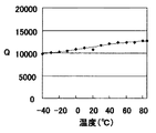
本実施形態のSAW共振子1について、以下の条件で周波数温度特性をシミュレーションした。
−本実施形態のSAW共振子1の基本データ
H:0.02λ
G:変化
IDTライン占有率η:0.6
反射器ライン占有率ηr:0.8
オイラー角:(0°,123°,43.5°)
IDT対数:120
電極指交差幅:40λ(λ=10μm)
反射器本数(片側あたり):60
電極指の傾斜角度:なし
For the
-Basic data H of the
G: Change IDT line occupancy η: 0.6
Reflector line occupancy ηr: 0.8
Euler angles: (0 °, 123 °, 43.5 °)
IDT logarithm: 120
Electrode finger crossing width: 40λ (λ = 10 μm)
Number of reflectors (per one side): 60
Electrode finger tilt angle: None
このシミュレーション結果を図3に示す。同図から分かるように、周波数温度特性は動作温度範囲(−40〜+85℃)において略3次曲線を示しており、周波数変動幅を20ppm以内という極めて小さな変動量に抑圧することできた。 The simulation result is shown in FIG. As can be seen from the figure, the frequency-temperature characteristic shows a substantially cubic curve in the operating temperature range (−40 to + 85 ° C.), and the frequency fluctuation range can be suppressed to an extremely small fluctuation amount of 20 ppm or less.
図3の周波数温度特性を示すSAW共振子1について、周波数、等価回路定数、及び静特性をまとめると、以下の表1になる。
SAW共振子1は、IDT3のストップバンド上端の周波数ft2と、反射器4のストップバンド下端の周波数fr1及びストップバンド上端の周波数fr2とが、fr1<ft2<fr2の関係を満たすように設定するのが好ましい。図4は、周波数に関するIDT3及び反射器4のSAW反射特性を示している。同図のように、周波数ft2を周波数fr1と周波数fr2との間に設定すると、周波数ft2において反射器4の反射係数がIDT3の反射係数よりも大きくなる。その結果、IDT3から励振されたストップバンド上端モードのSAWは、反射器4からIDT3側により高い反射係数で反射されることになる。従って、SAWの振動エネルギーを効率良く閉じ込めることができ、低損失なSAW共振子1を実現できる。
The
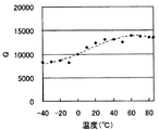
また、SAW共振子1のQ値について、電極指6a、6bの高さ即ち膜厚Hと電極指間溝8の深さGとにより形成される段差の大きさ(G+H)との関係をシミュレーションにより検証した。比較のため、電極指間に溝を設けずかつストップバンド上端モードの共振を用いる従来のSAW共振子について、以下の条件でQ値と電極指の高さ即ち膜厚との関係をシミュレーションした。
In addition, regarding the Q value of the
−従来のSAW共振子の基本データ
H:変化
G:ゼロ(無し)
IDTライン占有率η:0.4
反射器ライン占有率ηr:0.3
オイラー角(0°,123°,43.5°)
IDT対数:120
電極指交差幅:40λ(λ=10μm)
反射器本数(片側あたり):60
電極指の傾斜角度:なし
-Basic data H of conventional SAW resonator H: Change G: Zero (none)
IDT line occupancy η: 0.4
Reflector line occupancy ηr: 0.3
Euler angles (0 °, 123 °, 43.5 °)
IDT logarithm: 120
Electrode finger crossing width: 40λ (λ = 10 μm)
Number of reflectors (per one side): 60
Electrode finger tilt angle: None
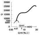
このシミュレーション結果を図5に示す。同図において、太線は本実施形態のSAW共振子1を、細線は従来のSAW共振子を示している。同図から分かるように、本実施形態のSAW共振子1は、段差(G+H)が0.0407λ(4.07%λ)以上の領域において、従来のSAW共振子よりも高いQ値を得ることができる。
The simulation result is shown in FIG. In the figure, a thick line indicates the
更に、本実施形態のSAW共振子においても、上述した傾斜型IDT構造を採用することによって、良好な周波数温度特性に加えて、Q値、CI値等の電気的特性を向上させ得ることが期待される。そこで、本願発明者は、本実施形態のSAW共振子に傾斜型IDT構造を採用し、IDT及び反射器を、電極指及び導体ストリップに直交する第1の方向第1の方向に対して、角度αをもって傾斜する第2の方向に配置した場合に、この傾斜角度αとオイラー角ψとの関係について更に検討を進めた。その結果、傾斜型IDT構造においても、広い動作温度範囲において優れた周波数温度特性と、良好な電気的特性即ちQ値及びCI値とを同時に実現し得ることを見出し、本発明を想到したものである。 Furthermore, in the SAW resonator of the present embodiment, it is expected that the electrical characteristics such as the Q value and the CI value can be improved in addition to the favorable frequency temperature characteristics by adopting the above-described tilted IDT structure. Is done. Therefore, the inventor of the present application employs an inclined IDT structure in the SAW resonator of this embodiment, and the IDT and the reflector are angled with respect to the first direction and the first direction perpendicular to the electrode fingers and the conductor strip. Further investigation was made on the relationship between the inclination angle α and the Euler angle ψ in the case of the arrangement in the second direction inclined with α. As a result, it has been found that even in an inclined IDT structure, excellent frequency temperature characteristics and good electrical characteristics, that is, Q value and CI value can be realized simultaneously in a wide operating temperature range, and the present invention has been conceived. is there.
本発明のSAWデバイスは、オイラー角(−1.5°≦φ≦1.5°,117°≦θ≦142°,42.79°≦|ψ|≦49.57°)の水晶基板と、
該水晶基板の主面に設けられた複数の電極指からなり、ストップバンド上端モードの弾性表面波を励振するIDTと、
弾性表面波の伝播方向に沿ってIDTを挟むようにその両側に配置した、それぞれ複数の導体ストリップからなる一対の反射器と、
IDTの隣り合う電極指間の水晶基板の表面に凹設した電極指間溝と、
反射器の隣り合う導体ストリップ間の水晶基板の表面に凹設した導体ストリップ間溝とを有し、
弾性表面波の波長λと電極指間溝の深さGとが、0.01λ≦Gの関係を満足し、
IDTのライン占有率ηと電極指間溝の深さGとが、
![]()
![]()
電極指及び導体ストリップに直交する第1の方向と水晶基板の電機軸とのなす角度がオイラー角ψであり、
IDT及び反射器の少なくとも一部が、第1の方向と角度αをもって交差する第2の方向に配置され、かつこの角度αが1.0°≦α≦2.75°の範囲内にあることを特徴とする。
The SAW device of the present invention includes a quartz substrate having an Euler angle (−1.5 ° ≦ φ ≦ 1.5 °, 117 ° ≦ θ ≦ 142 °, 42.79 ° ≦ | ψ | ≦ 49.57 °),
An IDT comprising a plurality of electrode fingers provided on the principal surface of the quartz substrate and exciting a surface acoustic wave in a stop band upper end mode;
A pair of reflectors each composed of a plurality of conductor strips arranged on both sides of the IDT so as to sandwich the IDT along the propagation direction of the surface acoustic wave;
A groove between the electrode fingers recessed in the surface of the quartz substrate between adjacent electrode fingers of the IDT;
A conductor strip groove recessed in the surface of the quartz substrate between adjacent conductor strips of the reflector;
The wavelength λ of the surface acoustic wave and the depth G of the interelectrode finger groove satisfy the relationship of 0.01λ ≦ G,
IDT line occupancy η and electrode finger groove depth G are:
![]()
![]()
The angle formed by the first direction orthogonal to the electrode fingers and the conductor strip and the electric axis of the quartz substrate is the Euler angle ψ,
At least a part of the IDT and the reflector are arranged in a second direction that intersects the first direction with an angle α, and the angle α is within a range of 1.0 ° ≦ α ≦ 2.75 °. It is characterized by.
このようにIDT及び反射器を配置することによって、SAWの振動エネルギーを効率良く閉じ込めることができる。その結果、後述するように広い動作温度範囲において、上述したオイラー角の面内回転STカット水晶板からなる水晶基板と電極指間溝とにより得られる良好な周波数温度特性を維持しつつ、それと同時に高いQ値及び低CI値の良好な電気的特性を実現し、発振安定性に優れたSAWデバイスを得ることができる。 By arranging the IDT and the reflector in this way, the SAW vibration energy can be confined efficiently. As a result, in a wide operating temperature range as will be described later, while maintaining the good frequency temperature characteristics obtained by the quartz substrate made of the above-described Euler angle in-plane rotating ST cut quartz plate and the inter-electrode finger groove, at the same time It is possible to obtain a SAW device that achieves good electrical characteristics such as a high Q value and a low CI value and is excellent in oscillation stability.
或る実施例では、角度αとオイラー角ψとが、ψ=1.06α+43.69°+0.05°の関係を満足することによって、広い動作温度範囲において高いQ値及び低CI値と共に、周波数変動量が極めて小さい優れた周波数温度特性を有するSAWデバイスを実現することができる。 In one embodiment, the angle α and the Euler angle ψ satisfy the relationship ψ = 1.06α + 43.69 ° + 0.05 °, thereby increasing the frequency along with the high Q value and low CI value over a wide operating temperature range. It is possible to realize a SAW device having an excellent frequency temperature characteristic with a very small fluctuation amount.
別の実施例では、IDTのライン占有率ηが、
更に別の実施例では、電極指間溝の深さGと電極指の膜厚Hとの和が、0.0407λ≦G+Hを満足することにより、ストップバンド上端モードの共振を用いた場合に、IDTの電極指間に溝を設けずにストップバンド下端モードの共振を用いる従来のSAW共振子従来の場合よりも高いQ値が得られる。 In still another embodiment, when the sum of the electrode finger groove depth G and the electrode finger film thickness H satisfies 0.0407λ ≦ G + H, when using the resonance of the stop band upper end mode, A conventional SAW resonator that uses resonance in the lower end mode of the stop band without providing a groove between the electrode fingers of the IDT can obtain a higher Q value than the conventional case.
また、別の実施例では、IDTを駆動するための発振回路を更に有することにより、広い動作温度範囲で周波数変動量が極めて小さく、CI値が低く、かつ発振安定性に優れたSAW発振器を得ることができる。 In another embodiment, by further including an oscillation circuit for driving the IDT, a SAW oscillator having an extremely small frequency variation, a low CI value and excellent oscillation stability in a wide operating temperature range is obtained. be able to.
本発明の別の側面によれば、上述した本発明のSAWデバイスを備え、それにより広い動作温度範囲で安定して良好な性能を発揮し得る電子機器、センサー装置が提供される。 According to another aspect of the present invention, there is provided an electronic apparatus and a sensor device that include the above-described SAW device of the present invention and can thereby stably exhibit good performance in a wide operating temperature range.
以下に、添付図面を参照しつつ、本発明の好適な実施例を詳細に説明する。尚、添付図面において、同一又は類似の構成要素には同一又は類似の参照符号を付して示す。 Hereinafter, preferred embodiments of the present invention will be described in detail with reference to the accompanying drawings. In the accompanying drawings, the same or similar components are denoted by the same or similar reference numerals.
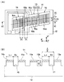
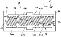
図6(A)(B)は、本発明によるSAWデバイスの第1実施例であるSAW共振子の構成を示している。本実施例のSAW共振子11は、矩形の水晶基板12と、該水晶基板の主面にそれぞれ形成されたIDT13と1対の反射器14,14とを有する。水晶基板12は、図1に関連して上述したSAW共振子1の水晶基板2と同じオイラー角(−1.5°≦φ≦1.5°,117°≦θ≦142°,42.79°≦|ψ|≦49.57°)の面内回転STカット水晶板を使用する。
6A and 6B show the configuration of a SAW resonator which is a first embodiment of a SAW device according to the present invention. The
IDT13は、それぞれ複数の電極指15a、15bからなり、かつそれらの基端部をバスバー16a,16bで接続した1対の櫛歯状電極13a,13bを有する。電極指15a、15b間に露出する水晶基板12の表面には、図6(B)に示すように、該表面をエッチング等で削除することによって、それぞれ一定深さの電極指間溝17が凹設されている。一方の櫛歯状電極13aの電極指15aと他方の櫛歯状電極13bの電極指15bとは、それらの延長方向と直交する向きに沿って交互にかつ所定の間隔を開けて一定のピッチPtで配列されている。
The
1対の反射器14,14は、SAWの伝搬方向に沿ってIDT13の両側に該IDTを挟むように配置されている。各反射器14は、それぞれ複数の導体ストリップ14a,14aを有する。導体ストリップ(電極指)14a,14a間に露出する水晶基板12の表面には、図6(B)に示すように、該表面をエッチング等で削除することによって、それぞれ一定深さの導体ストリップ間溝18が凹設されている。前記各導体ストリップは、IDT13の前記各電極指と同様に、それらの延長方向と直交する向きに沿って一定のピッチPrで配列されている。
The pair of
前記電極指及び導体ストリップは、例えばAlやAlを主体とする合金を用いた金属膜で同じ膜厚Hに形成される。電極指間溝17と導体ストリップ間溝18とは、同じ深さGに形成される。各反射器14,14の最も内側の前記導体ストリップとそれに隣り合うIDT13の最も外側の電極指15a(又は15b)との間も、同様に水晶基板表面を削除して、前記導体ストリップ間溝と同じ深さの溝が凹設されている。
The electrode fingers and the conductor strips are formed with the same film thickness H, for example, using a metal film made of Al or an alloy mainly composed of Al. The
上述したオイラー角の面内回転STカット水晶板からなる水晶基板12は、水晶の結晶異方性のため、IDT13によりSAWを励振させたとき、水晶基板12のX´軸の方向であるSAWの位相速度の方向19と、SAWエネルギーの伝搬方向である群速度の方向20とが異なる。SAWの位相速度の方向19(X´軸)と水晶の電気軸(X軸)とのなす角度がオイラー角ψである。群速度の方向20は、位相速度の方向19に対して傾斜角αをもって交差している。
Due to the crystal anisotropy of the quartz crystal, the
電極指15a、15b及び導体ストリップ14a,14aは、その延長方向が水晶基板12のX´軸即ちSAWの位相速度の方向19と直交するように形成されている。更に前記電極指及び導体ストリップは、群速度の方向20に沿って位相速度の方向19から角度α傾斜させた向きに配置されている。このとき、導体ストリップ14a,14aの群速度の方向20に直交する幅Wrを、電極指15a、15bの群速度の方向20に直交する方向の幅Wtと同じに設定することによって、SAWエネルギーは反射器14,14からの漏れを少なくし、効率良く閉じ込めることができる。
The
別の実施例では、少なくともIDT13の電極指及び反射器14,14の導体ストリップの一部が、群速度の方向20に沿って配置されていれば、SAWエネルギーの反射器14,14からの漏れを少なくすることができる。また、別の実施例では、前記導体ストリップの幅Wrを前記電極指の幅Wtより広く設定する。これによって、群速度の方向20に沿って伝搬するSAWエネルギーのほとんどを反射器14,14により反射し、閉じ込め効果を向上させることができる。
In another embodiment, the leakage of SAW energy from the
本実施例の傾斜型IDT構造では、群速度の方向20と位相速度の方向19とのなす角度αが、1.0°≦α≦2.75°の範囲内にあるように設定する。これにより、上述したオイラー角の面内回転STカット水晶板からなる水晶基板12及び電極指間溝17によって得られる良好な周波数温度特性を維持しつつ、高いQ値及び低インピーダンス化(低CI値)を達成することができる。
In the tilted IDT structure of the present embodiment, the angle α formed by the
更に本実施例では、角度αと水晶基板12のオイラー角ψとが、ψ=1.06α+43.69°±0.05°の関係を満足するように設定する。これにより、広い動作温度範囲において、高いQ値及び低CI値と共に、周波数変動量が極めて小さい優れた周波数温度特性を発揮するSAW共振子を実現することができる。
Further, in this embodiment, the angle α and the Euler angle ψ of the
このように構成することによって、SAW共振子11は、水晶基板12のX´軸方向から角度α傾斜した群速度の方向20及びY´軸方向の両方に振動変位成分を有するRayleigh型(レイリー型)のSAWを励起する。上述したオイラー角の水晶基板12を用いることによって、SAWの伝播方向が水晶の結晶軸であるX軸からずれているので、ストップバンド上端モードのSAWを励起することができる。
With this configuration, the
図6(B)に示すように、IDT13のライン占有率ηは、電極指15a、15bの線幅をLt、電極指間溝17の幅をStとして、η=Lt/(Lt+St)で表される。反射器14のライン占有率ηrは、導体ストリップ14aの線幅をLr、導体ストリップ間溝18の幅をSrとして、ηr=Lr/(Lr+Sr)で表される。
As shown in FIG. 6B, the line occupation ratio η of the
ここで、IDT13の電極指のピッチPt及び反射器14の導体ストリップのピッチPrについて説明する。交差する1対の櫛歯状電極13a,13bの各電極指ピッチPtと、電極指の線幅Lt及びb電極指間の幅(即ち、電極指間溝のSAW伝搬方向の幅)Stとの関係は、Lt+St=dtとしたとき、Pt=2×dt=2×(Lt+St)となる。即ち、SAW伝搬方向に見て、隣り合う電極指13aと電極指13bとの中心間距離dt(所謂、ラインアンドスペース)は、dt=Lt+Stとなる。従って、電極指ピッチPt=2×dt=λとなる。
Here, the pitch Pt of the electrode fingers of the
反射器14は、SAW伝搬方向に見て、隣り合う導体ストリップ14aの中心間距離drが、dr=Lr+Srとなる。この中心間距離drは、反射器14を伝搬するSAWの波長λの1/2、即ちdr=λ/2にする。従って、導体ストリップ14aのピッチPrは、Pr=2×dr=2×(Lr+Sr)となる。
When the
(実施例1)
SAW共振子11の仕様を次のように設定した。
水晶基板寸法:5.0×1.5(mm)
オイラー角:(0°,123°,45.8°)
IDT対数:180
反射器本数(片側あたり): 78
Example 1
The specifications of the
Crystal substrate dimensions: 5.0 x 1.5 (mm)
Euler angles: (0 °, 123 °, 45.8 °)
IDT logarithm: 180
Number of reflectors (per side): 78
IDT13は次のように設計した。
SAW波長λ:7.9(μm)、
電極材料:Al
電極指膜厚H:0.02λ(2%λ)=0.1580(μm)
電極指ピッチPt:λ/2=3.95(μm)、
電極指線幅Lt:0.625Pt=2.4688(μm)
(ライン占有率η:0.625)
SAW wavelength λ: 7.9 (μm),
Electrode material: Al
Electrode finger film thickness H: 0.02λ (2% λ) = 0.1580 (μm)
Electrode finger pitch Pt: λ / 2 = 3.95 (μm),
Electrode finger line width Lt: 0.625 Pt = 2.688 (μm)
(Line occupancy η: 0.625)
反射器14は次のように設計した。
電極材料:Al
導体ストリップ膜厚H:2%λ(0.02λ)=0.1580(μm)
導体ストリップピッチPr:λ/2=3.95(μm)、
導体ストリップ線幅:0.625Pt=2.4688(μm)
(ライン占有率η:0.625)
The
Electrode material: Al
Conductor strip film thickness H: 2% λ (0.02λ) = 0.1580 (μm)
Conductor strip pitch Pr: λ / 2 = 3.95 (μm)
Conductor strip line width: 0.625 Pt = 2.688 (μm)
(Line occupancy η: 0.625)
電極指間溝17は次のように設計した。
深さ:0.045λ(4.5%λ)=0.3555(μm)
電極指実効膜厚:0.065λ(6.5%λ)=0.5135(μm)
The
Depth: 0.045λ (4.5% λ) = 0.3555 (μm)
Electrode finger effective film thickness: 0.065λ (6.5% λ) = 0.5135 (μm)
このように設計したSAW共振子11について、傾斜角αが1.0≦α≦3.0の範囲で周波数温度特性の2次温度係数βが最適となる傾斜角αとオイラー角ψとの関係をシミュレーションした。この結果を図7に示す。同図において、プロットした黒丸点を結ぶ実線はβ=0となる場合を示している。また同図において、プロットした黒丸点を結ぶ破線は、|β|≦0.01となる場合の上限値を、プロットした三角形黒点を結ぶ破線はその下限値を示している。
With respect to the
同図から、前記上限値を示す破線と下限値を示す破線との間に、実施例1のSAW共振子11について2次温度係数|β|≦0.01の良好な周波数温度特性を発揮し得る傾斜角α及びオイラー角ψの範囲が存在することを確認できた。同図において、β=0となる傾斜角αとオイラー角ψとの関係を検証したところ、それらは次の条件式、
ψ=1.06α+43.69° …(4)
を満足することが判明した。更に、|β|≦0.01となる傾斜角αとオイラー角ψとの関係を検証したところ、それらは次の条件式、
ψ=1.06α+43.69°±0.05° …(5)
を満足することが判明した。
From this figure, between the broken line indicating the upper limit value and the broken line indicating the lower limit value, the
ψ = 1.06α + 43.69 ° (4)
Was found to satisfy. Further, when the relationship between the inclination angle α and Euler angle ψ satisfying | β | ≦ 0.01 is verified, they are expressed by the following conditional expression:
ψ = 1.06α + 43.69 ° ± 0.05 ° (5)
Was found to satisfy.
次に、実施例1のSAW共振子11について、傾斜角α=2°として周波数温度特性をシミュレーションした。このとき、水晶基板12のオイラー角ψ=45.8°は、傾斜角α=2°において上記条件式(4)を満足している。この結果を図8に示す。同図に示すように、−40℃〜+85℃の広い動作温度範囲において、周波数変動量が3次曲線で表される良好な周波数温度特性を有することが確認された。
Next, the frequency temperature characteristics of the
比較例として、水晶基板12のオイラー角ψをIDTの傾斜角αと同じ角度2°だけ回転させたψ=45.69°の場合について、周波数温度特性をシミュレーションした。この結果を図9に示す。同図に示すように、−40℃〜+85℃の広い動作温度範囲において、周波数温度特性は、傾斜角αが0°の場合、即ちIDT13が水晶基板のX´軸に対して傾斜していない従来のIDT構造よりも劣化している。このように本発明によれば、水晶基板12のオイラー角ψを上記条件式(4)、(5)のように設定することによって、良好な周波数温度特性が得られる。
As a comparative example, frequency temperature characteristics were simulated for a case where ψ = 45.69 °, where the Euler angle ψ of the
更に、実施例1のSAW共振子11について、傾斜角αと−40℃〜+85℃の広い動作温度範囲において最低値となるQ値との関係をシミュレーションした。その結果を図10に示す。同図において、傾斜角αが0°の場合、即ちIDT13が水晶基板のX´軸に対して傾斜していない従来のIDT構造では、Q値が1500未満である。これに対し、傾斜角αが1.0≦α≦2.75の範囲では、Q値が1800を超えており、従来構造よりも大幅に改善されていることを確認できた。
Furthermore, regarding the
(実施例2)
上記実施例1において、反射器14の導体ストリップ線幅を0.725Pr(=2.8638μm)、ライン占有率をηr=0.725に変更した。実施例2について、IDTの傾斜角α=0°,1.0°,1.5°,2.0°,2.5°,3.0°とした場合に、−40℃〜+85℃の広い動作温度範囲におけるQ値の変化をシミュレーションした。その結果を図11−1乃至図11−6に示す。
(Example 2)
In Example 1, the conductor strip line width of the
図11−2乃至図11−5から、傾斜角α=1.0°,1.5°,2.0°,2.5°の場合、Q値が動作温度範囲全体に亘って比較的安定して高い値を示すことが分かる。これに対し、傾斜角α=0°の場合、図11−1に示すように、低温側でQ値が低下している。傾斜角α=3.0°の場合、図11−6に示すように、低温側でQ値が著しく劣化している。実施例2の結果から、Q値の温度特性の観点から、1.0≦α≦2.5が傾斜角αの最適範囲であることが判明した。 From FIG. 11-2 to FIG. 11-5, when the inclination angle is α = 1.0 °, 1.5 °, 2.0 °, 2.5 °, the Q value is relatively stable over the entire operating temperature range. It can be seen that this shows a high value. On the other hand, when the inclination angle α = 0 °, as shown in FIG. 11A, the Q value decreases on the low temperature side. In the case of the inclination angle α = 3.0 °, as shown in FIG. 11-6, the Q value is significantly deteriorated on the low temperature side. From the results of Example 2, it was found that 1.0 ≦ α ≦ 2.5 is the optimum range of the inclination angle α from the viewpoint of the temperature characteristic of the Q value.
次に、実施例2について、傾斜角αと−40℃〜+85℃の広い動作温度範囲において最低値となるQ値との関係をシミュレーションした。この結果を図12に示す。同図に示すように、斜角αが0°である従来のIDT構造の場合、Q値が10000未満である。これに対し、傾斜角αが1.0≦α≦2.75の範囲では、Q値が12800を超えており、従来構造よりも大幅に改善されていることを確認できた。また、傾斜角αがα≧3.0の範囲では、Q値が10000未満に低下している。このように本発明のSAW共振子は、広い動作温度範囲で発振器として利用することができる。 Next, for Example 2, the relationship between the inclination angle α and the Q value that is the lowest value in a wide operating temperature range of −40 ° C. to + 85 ° C. was simulated. The result is shown in FIG. As shown in the figure, in the case of the conventional IDT structure in which the oblique angle α is 0 °, the Q value is less than 10,000. On the other hand, when the inclination angle α is in the range of 1.0 ≦ α ≦ 2.75, the Q value exceeds 12800, and it was confirmed that the structure was greatly improved over the conventional structure. In addition, in the range where the inclination angle α is α ≧ 3.0, the Q value is reduced to less than 10,000. Thus, the SAW resonator of the present invention can be used as an oscillator in a wide operating temperature range.
更に、傾斜角αと−40℃〜+85℃の広い動作温度範囲において最大となるCI値との関係をシミュレーションした。この結果を図13に示す。図13は、傾斜角αが0°である従来のIDT構造の場合、CI値が25Ωを超えているが、傾斜角αが1.0≦α≦2.5の範囲では、低いCI値が得られることを示している。一般にCI値は、Q値に反比例することが知られているが、このシミュレーション結果は、本発明によって高Q値化と同時に低CI値化を実現できることを示している。 Furthermore, the relationship between the inclination angle α and the maximum CI value in a wide operating temperature range of −40 ° C. to + 85 ° C. was simulated. The result is shown in FIG. FIG. 13 shows that in the case of the conventional IDT structure in which the inclination angle α is 0 °, the CI value exceeds 25Ω, but in the range where the inclination angle α is 1.0 ≦ α ≦ 2.5, a low CI value is obtained. It shows that it is obtained. In general, the CI value is known to be inversely proportional to the Q value, but this simulation result shows that the present invention can achieve a low CI value simultaneously with a high Q value.
更に本願発明者は、傾斜角α=2.0°の場合に、電極指膜厚H、電極指間溝の深さG、及びオイラー角θをパラメーターとして、周波数変動量が少ない3次曲線の優れた周波数温度特性と高いQ値とを実現し得るIDTライン占有率η、反射器ライン占有率ηr、2次温度係数と、その場合に得られるQ値とを算出した。その結果を以下の表2に示す。
一般にQ値は、SAWエネルギーの閉じ込め効果によって略決定され、言い換えれば反射器の反射効率即ち反射器の構造(反射器本数、実効膜厚、電極線幅、密度等)によって決定される。従って、水晶基板のカット角、例えばオイラー角θを多少変化させても、Q値にはほとんど影響しないはずである。表2から分かるように、オイラー角θを優れた周波数温度特性が得られる角度範囲内で117°、123°、142°に変化させたが、η<ηrにおいて全ての場合に、2次温度係数は−0.01〜+0.01ppm/℃2の良好な周波数温度特性が、Q値は概ね15000の高い値が得られる。 In general, the Q value is substantially determined by the confinement effect of the SAW energy, in other words, is determined by the reflection efficiency of the reflector, that is, the reflector structure (number of reflectors, effective film thickness, electrode line width, density, etc.). Therefore, even if the cut angle of the quartz substrate, for example, the Euler angle θ is slightly changed, the Q value should hardly be affected. As can be seen from Table 2, the Euler angle θ was changed to 117 °, 123 °, and 142 ° within an angular range where excellent frequency temperature characteristics were obtained. However, in all cases where η <ηr, the secondary temperature coefficient Has a good frequency-temperature characteristic of −0.01 to +0.01 ppm / ° C. 2 and a high Q value of about 15000 can be obtained.
従って、本発明によれば、オイラー角θ=117°〜142°の範囲で良好な周波数温度特性と高いQ値とを同時に実現できることが分かる。また、Q値は、傾斜角αを上述した最適範囲に設定することによって、電極指膜厚H、電極指間溝の深さG、オイラー角θ及びライン占有率に影響されることなく、改善できることが裏付けられた。 Therefore, according to the present invention, it can be seen that a good frequency temperature characteristic and a high Q value can be realized simultaneously in the range of Euler angle θ = 117 ° to 142 °. Further, the Q value is improved without being affected by the electrode finger film thickness H, the electrode finger groove depth G, the Euler angle θ, and the line occupancy rate by setting the inclination angle α in the optimum range described above. It was proved that we could do it.
本発明は、上述した本発明のSAW共振子と発振回路とを組み合わせて構成される発振器にも適用することができる。図14(A)、(B)は、そのような本発明によるSAWデバイスの第2実施例であるSAW発振器の典型例の構成を示している。本実施例のSAW発振器31は、本発明によるSAW共振子32と、該SAW共振子を駆動制御する発振回路としてIC(integrated circuit)33と、これらを収容するパッケージ34とを備える。SAW共振子32及びIC33は、パッケージ34の底板34a上に表面実装されている。
The present invention can also be applied to an oscillator configured by combining the above-described SAW resonator of the present invention and an oscillation circuit. FIGS. 14A and 14B show the configuration of a typical example of a SAW oscillator which is a second embodiment of the SAW device according to the present invention. The
SAW共振子32は、第1実施例のSAW共振子11と同様の構成を有し、第1実施例と同じオイラー角で表示される水晶基板35と、その表面に形成された1対の櫛歯状電極36a,36bからなるIDTと1対の反射器37,37とを有する。IC33の上面には、電極パッド38a〜38fが設けられている。パッケージ34の底板34a上には、電極パターン39a〜39gが形成されている。SAW共振子32の櫛歯状電極36a,36b及びIC33の電極パッド38a〜38fは、それぞれボンディングワイヤ40,41により対応する電極パターン39a〜39gと電気的に接続されている。このようにSAW共振子32及びIC33を搭載したパッケージ34は、その上部に接合されたリッド42により気密に封止されている。
The
本実施例のSAW発振器31は、本発明のSAW共振子を備えることによって、広い動作温度範囲で周波数変動量が極めて小さい優れた周波数温度特性を有すると共に、高いQ値を有するので、安定した発振動作が可能であり、更に低インピーダンス化による消費電力の低減を実現することができる。その結果、近年の情報通信の高速化に基づく高周波化及び高精度化の要求に対応し、低温から高温まで温度が大きく変動するような環境下でも長期に安定して動作する優れた耐環境特性を備えたSAW発振器が得られる。
Since the
本発明は、上記実施例に限定されるものでなく、その技術的範囲内で様々な変形又は変更を加えて実施することができる。例えば、IDTの電極構造は、上記実施例以外に、公知の様々な構成を採用することができる。また、本発明は、上述したSAW共振子、SAW発振器以外の様々なSAWデバイスに同様に適用することができる。更に本発明のSAWデバイスは、例えば携帯電話、ハードディスク、パーソナルコンピューター、BS及びCS放送用の受信チューナー、同軸ケーブルや光ケーブル中を伝搬する高周波信号や光信号用の各種処理装置、広い温度範囲で高周波・高精度クロック(低ジッタ、低位相雑音)を必要とするサーバー・ネットワーク機器、無線通信用機器等の様々な電子機器、各種モジュール装置や、圧力センサー、加速度センサー、回転速度センサー等の各種センサー装置にも広く適用することができる。 The present invention is not limited to the above embodiments, and can be implemented with various modifications or changes within the technical scope thereof. For example, the electrode structure of the IDT can adopt various known configurations other than the above-described embodiments. Further, the present invention can be similarly applied to various SAW devices other than the above-described SAW resonator and SAW oscillator. Further, the SAW device of the present invention includes, for example, a mobile phone, a hard disk, a personal computer, a reception tuner for BS and CS broadcasting, a high-frequency signal propagating in a coaxial cable or an optical cable, various processing devices for optical signals, and a high-frequency over a wide temperature range.・ Various electronic devices such as server / network equipment and wireless communication equipment that require high precision clock (low jitter, low phase noise), various module devices, various sensors such as pressure sensor, acceleration sensor, rotation speed sensor, etc. The present invention can be widely applied to apparatuses.
1,11,32,51…SAW共振子、2,12,35,52,62…水晶基板、3,13,53,63…IDT、3a,3b,13a,13b,36a,36b,53a,53b,63a,63b…櫛歯状電極、4,14,37,54,64…反射器、4a,14a,54a,64a…導体ストリップ、5…ウエーハ、5a…面、6a,6b,15a,15b,55a,55b,65a,65b…電極指、7a,7b,16a,16b…バスバー、8,17…電極指間溝、9,18…導体ストリップ間溝、31…SAW発振器、33…IC、34…パッケージ、34a…底板、38a〜38f…電極パッド、39a〜39g…電極パターン、40,41…ボンディングワイヤ、42…リッド。
1, 11, 32, 51... SAW resonator, 2, 12, 35, 52, 62... Quartz substrate, 3, 13, 53, 63... IDT, 3a, 3b, 13a, 13b, 36a, 36b, 53a,
Claims (7)
前記水晶基板の主面に設けられた複数の電極指からなり、ストップバンド上端モードの弾性表面波を励振するIDTと、
前記弾性表面波の伝播方向に沿って前記IDTを挟むようにその両側に配置した、それぞれ複数の導体ストリップからなる一対の反射器と、
前記IDTの隣り合う前記電極指間の前記水晶基板の表面に凹設した電極指間溝と、
前記反射器の隣り合う前記導体ストリップ間の前記水晶基板の表面に凹設した導体ストリップ間溝とを有し、
前記弾性表面波の波長λと前記電極指間溝の深さGとが、0.01λ≦Gの関係を満足し、
前記IDTのライン占有率ηと前記電極指間溝の深さGとが、
前記電極指及び前記導体ストリップに直交する第1の方向と前記水晶基板の電機軸とのなす角度が前記オイラー角ψであり、
前記IDT及び反射器の少なくとも一部が、前記第1の方向と角度αをもって交差する第2の方向に配置され、かつ前記角度αが1.0°≦α≦2.75°の範囲内にあることを特徴とする弾性表面波デバイス。 A quartz substrate with Euler angles (−1.5 ° ≦ φ ≦ 1.5 °, 117 ° ≦ θ ≦ 142 °, 42.79 ° ≦ | ψ | ≦ 49.57 °);
An IDT comprising a plurality of electrode fingers provided on the principal surface of the quartz substrate and exciting a surface acoustic wave in a stop band upper end mode;
A pair of reflectors each composed of a plurality of conductor strips, disposed on both sides of the IDT so as to sandwich the surface acoustic wave in the propagation direction;
A groove between the electrode fingers recessed in the surface of the quartz substrate between the electrode fingers adjacent to the IDT;
A conductor strip groove recessed in the surface of the quartz substrate between the conductor strips adjacent to the reflector;
The wavelength λ of the surface acoustic wave and the depth G of the inter-electrode finger groove satisfy a relationship of 0.01λ ≦ G,
The line occupation ratio η of the IDT and the depth G of the inter-electrode finger groove are:
The angle formed by the first direction perpendicular to the electrode fingers and the conductor strip and the electrical axis of the quartz substrate is the Euler angle ψ.
At least a part of the IDT and the reflector are arranged in a second direction intersecting the first direction with an angle α, and the angle α is within a range of 1.0 ° ≦ α ≦ 2.75 °. There is provided a surface acoustic wave device.
Priority Applications (3)
| Application Number | Priority Date | Filing Date | Title |
|---|---|---|---|
| JP2010201749A JP2012060418A (en) | 2010-09-09 | 2010-09-09 | Surface acoustic wave device, electronic apparatus and sensor device |
| CN201110247975.0A CN102403978B (en) | 2010-09-09 | 2011-08-26 | Surface acoustic wave device, electronic apparatus, and sensor apparatus |
| US13/223,530 US8723395B2 (en) | 2010-09-09 | 2011-09-01 | Surface acoustic wave device, electronic apparatus, and sensor apparatus |
Applications Claiming Priority (1)
| Application Number | Priority Date | Filing Date | Title |
|---|---|---|---|
| JP2010201749A JP2012060418A (en) | 2010-09-09 | 2010-09-09 | Surface acoustic wave device, electronic apparatus and sensor device |
Publications (2)
| Publication Number | Publication Date |
|---|---|
| JP2012060418A true JP2012060418A (en) | 2012-03-22 |
| JP2012060418A5 JP2012060418A5 (en) | 2013-10-17 |
Family
ID=45805968
Family Applications (1)
| Application Number | Title | Priority Date | Filing Date |
|---|---|---|---|
| JP2010201749A Pending JP2012060418A (en) | 2010-09-09 | 2010-09-09 | Surface acoustic wave device, electronic apparatus and sensor device |
Country Status (3)
| Country | Link |
|---|---|
| US (1) | US8723395B2 (en) |
| JP (1) | JP2012060418A (en) |
| CN (1) | CN102403978B (en) |
Families Citing this family (16)
| Publication number | Priority date | Publication date | Assignee | Title |
|---|---|---|---|---|
| US8952596B2 (en) * | 2009-02-27 | 2015-02-10 | Seiko Epson Corporation | Surface acoustic wave resonator, surface acoustic wave oscillator, and electronic instrument |
| JP4645923B2 (en) * | 2009-02-27 | 2011-03-09 | セイコーエプソン株式会社 | Surface acoustic wave resonator and surface acoustic wave oscillator |
| JP5678486B2 (en) | 2010-06-17 | 2015-03-04 | セイコーエプソン株式会社 | Surface acoustic wave resonator, surface acoustic wave oscillator and electronic device |
| JP5934464B2 (en) | 2010-08-26 | 2016-06-15 | セイコーエプソン株式会社 | Surface acoustic wave resonator, surface acoustic wave oscillator, and electronic device |
| JP2012049818A (en) | 2010-08-26 | 2012-03-08 | Seiko Epson Corp | Surface acoustic wave resonator, surface acoustic wave oscillator, and electronic apparatus |
| JP2012049817A (en) | 2010-08-26 | 2012-03-08 | Seiko Epson Corp | Surface acoustic wave device, surface acoustic wave oscillator, and electronic apparatus |
| JP2012060421A (en) | 2010-09-09 | 2012-03-22 | Seiko Epson Corp | Surface acoustic wave device, electronic apparatus and sensor device |
| JP2012060419A (en) | 2010-09-09 | 2012-03-22 | Seiko Epson Corp | Surface acoustic wave device, electronic apparatus and sensor device |
| JP2012060418A (en) | 2010-09-09 | 2012-03-22 | Seiko Epson Corp | Surface acoustic wave device, electronic apparatus and sensor device |
| JP2012060422A (en) * | 2010-09-09 | 2012-03-22 | Seiko Epson Corp | Surface acoustic wave device, electronic apparatus and sensor device |
| JP2012060420A (en) * | 2010-09-09 | 2012-03-22 | Seiko Epson Corp | Surface acoustic wave device, electronic apparatus and sensor device |
| CN105393455B (en) * | 2013-06-28 | 2017-04-12 | 大河晶振科技有限公司 | Elastic wave device |
| WO2015098756A1 (en) * | 2013-12-26 | 2015-07-02 | 株式会社村田製作所 | Elastic wave device and filter apparatus |
| CN105245199B (en) * | 2015-10-28 | 2018-08-03 | 江苏声立传感技术有限公司 | High q-factor one-port saw resonator applied to radio temperature sensor |
| CN107241077B (en) * | 2017-05-12 | 2020-12-29 | 电子科技大学 | Piezoelectric film bulk acoustic resonator and preparation method thereof |
| US11621691B2 (en) * | 2018-07-16 | 2023-04-04 | Qorvo Us, Inc. | Reflective structures for surface acoustic wave devices |
Citations (11)
| Publication number | Priority date | Publication date | Assignee | Title |
|---|---|---|---|---|
| JPS575418A (en) * | 1980-06-13 | 1982-01-12 | Nippon Telegr & Teleph Corp <Ntt> | Cavity type surface elastic wave resonator |
| JPS5799813A (en) * | 1980-12-13 | 1982-06-21 | Nippon Telegr & Teleph Corp <Ntt> | Surface acoustic wave resonator |
| JPS6468114A (en) * | 1987-09-09 | 1989-03-14 | Hiroshi Shimizu | Structure for idt exciting type piezoelectric resonator |
| JP3216137B2 (en) * | 1994-09-29 | 2001-10-09 | セイコーエプソン株式会社 | SAW device |
| JP2003188675A (en) * | 2001-12-19 | 2003-07-04 | Alps Electric Co Ltd | Surface acoustic wave element and duplexer provided therewith |
| JP2005204275A (en) * | 2003-12-12 | 2005-07-28 | Seiko Epson Corp | Surface acoustic wave element piece, its manufacturing method, and surface acoustic wave device |
| JP2006203408A (en) * | 2005-01-19 | 2006-08-03 | Epson Toyocom Corp | Surface acoustic wave device |
| JP2009225420A (en) * | 2008-02-20 | 2009-10-01 | Epson Toyocom Corp | Surface acoustic wave device and surface acoustic wave oscillator |
| JP2010016523A (en) * | 2008-07-02 | 2010-01-21 | Murata Mfg Co Ltd | Elastic wave resonator and ladder type filter |
| JP2010103720A (en) * | 2008-10-23 | 2010-05-06 | Epson Toyocom Corp | Surface acoustic wave device |
| WO2010098139A1 (en) * | 2009-02-27 | 2010-09-02 | エプソントヨコム株式会社 | Surface acoustic wave resonator, surface acoustic wave oscillator, and electronic device |
Family Cites Families (41)
| Publication number | Priority date | Publication date | Assignee | Title |
|---|---|---|---|---|
| GB2078042B (en) | 1980-06-13 | 1984-08-08 | Nippon Telegraph & Telephone | Surface acoustic wave resonator |
| JPS6192011A (en) | 1984-10-11 | 1986-05-10 | Nec Kansai Ltd | Manufacture of surface acoustic wave element |
| JPS6388910A (en) | 1986-10-02 | 1988-04-20 | Toyo Commun Equip Co Ltd | Surface acoustic wave resonator |
| JPS6434411A (en) | 1987-07-29 | 1989-02-03 | Hitachi Ltd | Controlling device for injection amount of flocculant in purification plant |
| JPH01231412A (en) | 1988-03-11 | 1989-09-14 | Fujitsu Ltd | Method for adjusting frequency characteristic of surface acoustic wave device |
| JPH02189011A (en) | 1989-01-18 | 1990-07-25 | Fujitsu Ltd | Manufacture of surface acoustic wave device |
| JP2839104B2 (en) | 1990-01-20 | 1998-12-16 | 株式会社シマノ | Transmission for fishing reel |
| JPH03266846A (en) | 1990-03-16 | 1991-11-27 | Konica Corp | Processing method and processing device for photosensitive planographic printing plate |
| JPH0590865A (en) | 1991-09-30 | 1993-04-09 | Oki Electric Ind Co Ltd | Central frequency adjusting method for acoustic surface wave filter |
| JP3411124B2 (en) | 1994-05-13 | 2003-05-26 | 松下電器産業株式会社 | Method for manufacturing surface acoustic wave module element |
| US5815900A (en) | 1995-03-06 | 1998-10-06 | Matsushita Electric Industrial Co., Ltd. | Method of manufacturing a surface acoustic wave module |
| JPH10270974A (en) | 1997-03-25 | 1998-10-09 | Kenwood Corp | Surface acoustic wave element |
| JP3266846B2 (en) | 1998-01-20 | 2002-03-18 | 東洋通信機株式会社 | Reflection inversion type surface acoustic wave converter and filter |
| CN1221074C (en) | 1999-11-16 | 2005-09-28 | 三菱电机株式会社 | Elastic wave device |
| JP2002100959A (en) | 2000-09-25 | 2002-04-05 | Toyo Commun Equip Co Ltd | Surface acoustic wave device |
| AUPR507601A0 (en) * | 2001-05-21 | 2001-06-14 | Microtechnology Centre Management Limited | Surface acoustic wave sensor |
| JP3622202B2 (en) | 2001-08-29 | 2005-02-23 | セイコーエプソン株式会社 | Method for adjusting temperature characteristics of surface acoustic wave device |
| JP2003283282A (en) | 2002-01-15 | 2003-10-03 | Murata Mfg Co Ltd | Electronic component having electrodes, its manufacturing method and communication apparatus |
| JP3826877B2 (en) | 2002-01-22 | 2006-09-27 | 株式会社村田製作所 | Surface acoustic wave device and communication device having the same |
| JP2004274696A (en) * | 2002-10-04 | 2004-09-30 | Seiko Epson Corp | Surface acoustic wave device and temperature characteristic adjustment method of surface acoustic wave device |
| JP4306458B2 (en) * | 2003-03-20 | 2009-08-05 | セイコーエプソン株式会社 | Voltage controlled oscillator, clock converter and electronic device |
| JP4246604B2 (en) | 2003-11-18 | 2009-04-02 | 富士通メディアデバイス株式会社 | Surface acoustic wave device |
| WO2005099089A1 (en) | 2004-04-01 | 2005-10-20 | Toyo Communication Equipment Co., Ltd. | Surface acoustic device |
| JP2006013576A (en) | 2004-06-22 | 2006-01-12 | Epson Toyocom Corp | Saw device and apparatus employing the same |
| JP2006148622A (en) | 2004-11-22 | 2006-06-08 | Seiko Epson Corp | Surface acoustic wave device and electronic equipment |
| US7382217B2 (en) * | 2004-12-03 | 2008-06-03 | Epson Toyocom Corporation | Surface acoustic wave device |
| JP3851336B1 (en) | 2005-05-31 | 2006-11-29 | 隆彌 渡邊 | Surface acoustic wave device |
| WO2006137464A1 (en) | 2005-06-21 | 2006-12-28 | Epson Toyocom Corporation | Elastic surface wave device, module, and oscillator |
| JP4412292B2 (en) | 2006-02-06 | 2010-02-10 | セイコーエプソン株式会社 | Surface acoustic wave device and electronic apparatus |
| JP2007267033A (en) | 2006-03-28 | 2007-10-11 | Epson Toyocom Corp | Surface acoustic wave element and surface acoustic wave device |
| JP4968510B2 (en) * | 2006-04-27 | 2012-07-04 | セイコーエプソン株式会社 | Method for adjusting frequency-temperature characteristics of surface acoustic wave element piece, surface acoustic wave element piece, and surface acoustic wave device |
| JP2007300287A (en) | 2006-04-28 | 2007-11-15 | Epson Toyocom Corp | Surface acoustic wave element, surface acoustic wave device, and electronic apparatus |
| US7504705B2 (en) | 2006-09-29 | 2009-03-17 | International Business Machines Corporation | Striped on-chip inductor |
| JP4645923B2 (en) * | 2009-02-27 | 2011-03-09 | セイコーエプソン株式会社 | Surface acoustic wave resonator and surface acoustic wave oscillator |
| JP5678486B2 (en) | 2010-06-17 | 2015-03-04 | セイコーエプソン株式会社 | Surface acoustic wave resonator, surface acoustic wave oscillator and electronic device |
| JP5934464B2 (en) | 2010-08-26 | 2016-06-15 | セイコーエプソン株式会社 | Surface acoustic wave resonator, surface acoustic wave oscillator, and electronic device |
| JP2012060422A (en) | 2010-09-09 | 2012-03-22 | Seiko Epson Corp | Surface acoustic wave device, electronic apparatus and sensor device |
| JP2012060418A (en) | 2010-09-09 | 2012-03-22 | Seiko Epson Corp | Surface acoustic wave device, electronic apparatus and sensor device |
| JP2012060420A (en) * | 2010-09-09 | 2012-03-22 | Seiko Epson Corp | Surface acoustic wave device, electronic apparatus and sensor device |
| JP2012060421A (en) * | 2010-09-09 | 2012-03-22 | Seiko Epson Corp | Surface acoustic wave device, electronic apparatus and sensor device |
| JP5648908B2 (en) | 2010-12-07 | 2015-01-07 | セイコーエプソン株式会社 | Vibration device, oscillator, and electronic device |
-
2010
- 2010-09-09 JP JP2010201749A patent/JP2012060418A/en active Pending
-
2011
- 2011-08-26 CN CN201110247975.0A patent/CN102403978B/en not_active Expired - Fee Related
- 2011-09-01 US US13/223,530 patent/US8723395B2/en active Active
Patent Citations (11)
| Publication number | Priority date | Publication date | Assignee | Title |
|---|---|---|---|---|
| JPS575418A (en) * | 1980-06-13 | 1982-01-12 | Nippon Telegr & Teleph Corp <Ntt> | Cavity type surface elastic wave resonator |
| JPS5799813A (en) * | 1980-12-13 | 1982-06-21 | Nippon Telegr & Teleph Corp <Ntt> | Surface acoustic wave resonator |
| JPS6468114A (en) * | 1987-09-09 | 1989-03-14 | Hiroshi Shimizu | Structure for idt exciting type piezoelectric resonator |
| JP3216137B2 (en) * | 1994-09-29 | 2001-10-09 | セイコーエプソン株式会社 | SAW device |
| JP2003188675A (en) * | 2001-12-19 | 2003-07-04 | Alps Electric Co Ltd | Surface acoustic wave element and duplexer provided therewith |
| JP2005204275A (en) * | 2003-12-12 | 2005-07-28 | Seiko Epson Corp | Surface acoustic wave element piece, its manufacturing method, and surface acoustic wave device |
| JP2006203408A (en) * | 2005-01-19 | 2006-08-03 | Epson Toyocom Corp | Surface acoustic wave device |
| JP2009225420A (en) * | 2008-02-20 | 2009-10-01 | Epson Toyocom Corp | Surface acoustic wave device and surface acoustic wave oscillator |
| JP2010016523A (en) * | 2008-07-02 | 2010-01-21 | Murata Mfg Co Ltd | Elastic wave resonator and ladder type filter |
| JP2010103720A (en) * | 2008-10-23 | 2010-05-06 | Epson Toyocom Corp | Surface acoustic wave device |
| WO2010098139A1 (en) * | 2009-02-27 | 2010-09-02 | エプソントヨコム株式会社 | Surface acoustic wave resonator, surface acoustic wave oscillator, and electronic device |
Also Published As
| Publication number | Publication date |
|---|---|
| US20120062069A1 (en) | 2012-03-15 |
| CN102403978B (en) | 2015-04-01 |
| US8723395B2 (en) | 2014-05-13 |
| CN102403978A (en) | 2012-04-04 |
Similar Documents
| Publication | Publication Date | Title |
|---|---|---|
| JP2012060418A (en) | Surface acoustic wave device, electronic apparatus and sensor device | |
| US8723394B2 (en) | Surface acoustic wave device, electronic apparatus, and sensor apparatus | |
| JP5678486B2 (en) | Surface acoustic wave resonator, surface acoustic wave oscillator and electronic device | |
| JP2012060422A (en) | Surface acoustic wave device, electronic apparatus and sensor device | |
| US9048806B2 (en) | Surface acoustic wave device, electronic apparatus, and sensor apparatus | |
| JP5574200B2 (en) | Surface acoustic wave resonator, surface acoustic wave oscillator, and electronic device | |
| JP4591800B2 (en) | Surface acoustic wave device and surface acoustic wave oscillator | |
| JP2012060419A (en) | Surface acoustic wave device, electronic apparatus and sensor device | |
| EP2224591B1 (en) | Surface acoustic wave resonator and surface acoustic wave oscillator | |
| JP5934464B2 (en) | Surface acoustic wave resonator, surface acoustic wave oscillator, and electronic device | |
| JP5652606B2 (en) | Surface acoustic wave resonator, surface acoustic wave oscillator, and electronic device | |
| JP2007300287A (en) | Surface acoustic wave element, surface acoustic wave device, and electronic apparatus | |
| JP2012124677A (en) | Vibrating device, oscillator and electronic apparatus | |
| JP2012049817A (en) | Surface acoustic wave device, surface acoustic wave oscillator, and electronic apparatus | |
| JP2012060417A (en) | Surface acoustic wave device, electronic apparatus and sensor device | |
| JP5850109B2 (en) | Surface acoustic wave resonator, surface acoustic wave oscillator, and electronic device | |
| JP5737490B2 (en) | Transversal surface acoustic wave device, surface acoustic wave oscillator and electronic equipment | |
| JP2015084534A (en) | Two-terminal pair surface acoustic wave resonator, surface acoustic wave oscillator, and electronic apparatus | |
| JP5750683B2 (en) | Two-terminal-pair surface acoustic wave resonator, surface acoustic wave oscillator and electronic device | |
| JP2015029358A (en) | Surface acoustic wave resonator, surface acoustic wave oscillator, and electronic device | |
| JP2012049631A (en) | Surface acoustic wave resonator, surface acoustic wave oscillator, electronic apparatus | |
| JP2015084535A (en) | Transversal type surface acoustic wave device, surface acoustic wave oscillator, and electronic apparatus |
Legal Events
| Date | Code | Title | Description |
|---|---|---|---|
| RD04 | Notification of resignation of power of attorney |
Free format text: JAPANESE INTERMEDIATE CODE: A7424 Effective date: 20120726 |
|
| A521 | Written amendment |
Free format text: JAPANESE INTERMEDIATE CODE: A523 Effective date: 20130830 |
|
| A621 | Written request for application examination |
Free format text: JAPANESE INTERMEDIATE CODE: A621 Effective date: 20130830 |
|
| A977 | Report on retrieval |
Free format text: JAPANESE INTERMEDIATE CODE: A971007 Effective date: 20140220 |
|
| A131 | Notification of reasons for refusal |
Free format text: JAPANESE INTERMEDIATE CODE: A131 Effective date: 20140304 |
|
| A521 | Written amendment |
Free format text: JAPANESE INTERMEDIATE CODE: A523 Effective date: 20140430 |
|
| A131 | Notification of reasons for refusal |
Free format text: JAPANESE INTERMEDIATE CODE: A131 Effective date: 20140805 |
|
| A521 | Written amendment |
Free format text: JAPANESE INTERMEDIATE CODE: A523 Effective date: 20141003 |
|
| RD03 | Notification of appointment of power of attorney |
Free format text: JAPANESE INTERMEDIATE CODE: A7423 Effective date: 20141003 |
|
| A02 | Decision of refusal |
Free format text: JAPANESE INTERMEDIATE CODE: A02 Effective date: 20150224 |