WO2025115059A1 - 回路基板、半導体装置、回路基板の製造方法および半導体装置の製造方法 - Google Patents
回路基板、半導体装置、回路基板の製造方法および半導体装置の製造方法 Download PDFInfo
- Publication number
- WO2025115059A1 WO2025115059A1 PCT/JP2023/042326 JP2023042326W WO2025115059A1 WO 2025115059 A1 WO2025115059 A1 WO 2025115059A1 JP 2023042326 W JP2023042326 W JP 2023042326W WO 2025115059 A1 WO2025115059 A1 WO 2025115059A1
- Authority
- WO
- WIPO (PCT)
- Prior art keywords
- recesses
- metal plate
- circuit board
- recess
- semiconductor device
- Prior art date
- Legal status (The legal status is an assumption and is not a legal conclusion. Google has not performed a legal analysis and makes no representation as to the accuracy of the status listed.)
- Pending
Links
Images







Classifications
-
- H—ELECTRICITY
- H10—SEMICONDUCTOR DEVICES; ELECTRIC SOLID-STATE DEVICES NOT OTHERWISE PROVIDED FOR
- H10W—GENERIC PACKAGES, INTERCONNECTIONS, CONNECTORS OR OTHER CONSTRUCTIONAL DETAILS OF DEVICES COVERED BY CLASS H10
- H10W70/00—Package substrates; Interposers; Redistribution layers [RDL]
- H10W70/60—Insulating or insulated package substrates; Interposers; Redistribution layers
Definitions
- This disclosure relates to a circuit board, a semiconductor device, a method for manufacturing a circuit board, and a method for manufacturing a semiconductor device.
- the semiconductor elements inside power semiconductor devices used in inverters and the like are bonded to the surface of a metal substrate that is placed on a ceramic substrate.
- a resin such as epoxy resin.
- the resin may peel off from the metal plate due to thermal stress during the manufacturing process of the semiconductor device or when the semiconductor device is in operation.
- Patent Document 1 discloses a semiconductor device in which multiple holes are formed in a conductive plate to which a power semiconductor chip is bonded. The holes create an anchor effect, improving adhesion between the molded resin and the conductive plate.
- the spacing between multiple semiconductor elements and the distance between the semiconductor elements and the edge of the metal plate tend to shrink. This also reduces the space available for forming recesses to improve adhesion between the resin and the metal plate, making it difficult to ensure sufficient adhesive strength between the resin and the metal plate.
- This disclosure has been made to solve the above problems, and aims to provide a circuit board that improves the adhesive strength between the resin and the metal plate and enables the miniaturization of semiconductor devices.
- the circuit board according to the present disclosure includes an insulating plate and a metal plate.
- the metal plate is bonded to an upper surface of the insulating plate.
- the metal plate includes a plurality of recesses provided on the surface of the metal plate.
- the minimum distance between adjacent recesses is 0.2 mm or less.
- the width of each of the plurality of recesses is 0.2 mm or less.
- the depth of each of the plurality of recesses is less than 0.05 mm.
- This disclosure provides a circuit board that improves the adhesive strength between the resin and the metal plate and enables the miniaturization of semiconductor devices.
- FIG. 1 is a plan view showing a configuration of a circuit board according to a first embodiment.
- 1 is a cross-sectional view showing a configuration of a semiconductor device in a first embodiment.
- FIG. 4 is an enlarged plan view showing the configuration of a recess;
- FIG. 4 is a cross-sectional view showing a configuration of a recess.
- FIG. 13 is a diagram showing the relationship between the minimum distance between adjacent recesses and adhesive strength. 13 is a diagram showing the appearance of the metal plate and the resin part after a shear test.
- FIG. 13 is a diagram showing the appearance of the metal plate and the resin part after a shear test.
- FIG. FIG. 13 is a plan view showing a configuration of a circuit board in a first modified example of the first embodiment.
- FIG. 4 is an enlarged plan view showing the configuration of a recess;
- FIG. 11 is a cross-sectional view showing a configuration of a recess in a second modification of the first embodiment.
- FIG. 11 is a cross-sectional view showing a configuration of a recess in a second modification of the first embodiment.
- FIG. 11 is a cross-sectional view showing a configuration of a recess in a second modification of the first embodiment.
- 11 is a cross-sectional view showing a configuration of a recessed portion of a circuit board according to a second embodiment.
- FIG. FIG. 11 is a plan view showing a configuration of a circuit board in a third embodiment.
- 13 is a cross-sectional view showing a configuration of a recess in a circuit board according to a fourth embodiment.
- FIG. FIG. 13 is a plan view showing a configuration of a circuit board in a fifth embodiment.
- Fig. 1 is a plan view showing the configuration of a circuit board 101 in embodiment 1.
- Fig. 2 is a cross-sectional view showing the configuration of a semiconductor device 201 in embodiment 1.
- Fig. 2 shows a cut surface taken along line AA' in Fig. 1.
- the circuit board 101 includes an insulating plate 10, a metal plate 20, and a heat sink 30.
- the semiconductor device 201 includes a circuit board 101, a semiconductor element 40, and a resin part 50.
- the semiconductor device 201 is mounted on a power conversion device such as an inverter, for example.
- the insulating plate 10 is made of an inorganic material such as ceramic.
- the heat sink 30 is bonded to the bottom surface of the insulating plate 10.
- the metal plate 20 is bonded to the top surface of the insulating plate 10.
- the metal plate 20 is made of, for example, copper, aluminum, etc.
- the metal plate 20 includes a plurality of recesses 21.
- the plurality of recesses 21 are provided on the surface of the metal plate 20.
- the recesses 21 are provided so as to surround a semiconductor element mounting area 41.
- the semiconductor element mounting area 41 is a predetermined area on the surface of the metal plate 20, and corresponds to the area where the semiconductor element 40 described below is mounted.
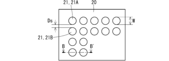
- FIG. 3 is an enlarged plan view showing the configuration of the recess 21.
- FIG. 3 shows the planar configuration of the region P in FIG. 1.
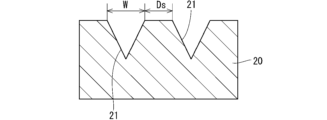
- FIG. 4 is a cross-sectional view showing the configuration of the recess 21.
- FIG. 4 shows a cut surface along B-B' in FIG. 3.
- the recess 21 is a non-through hole.
- the planar shape of the recess 21 is circular.
- the minimum distance Ds between adjacent recesses 21 is 0.2 mm or less. When the adjacent recesses 21 are defined as the first recess 21A and the second recess 21B, the minimum distance Ds is not the distance between the center of the first recess 21A and the center of the second recess 21B.
- the minimum distance Ds corresponds to the distance between the sidewall of the first recess 21A and the sidewall of the second recess 21B at their closest points.
- the diameter of the recess 21, i.e., the width W of the recess 21, is 0.2 mm or less.
- the depth Dp of the recess 21 is less than 0.05 mm.
- the semiconductor element 40 is bonded to the surface of the metal plate 20 via a bonding material 61.
- the semiconductor element 40 is mounted in a semiconductor element mounting area 41.
- the bonding material 61 is formed of a conductive material such as solder or a sintered material.
- the sintered material includes, for example, Ag or Cu.
- the semiconductor element 40 is formed of a semiconductor such as Si.
- the semiconductor is preferably a so-called wide band gap semiconductor such as SiC, GaN, Ga 2 O 3 , GeO 2 , or diamond.
- the semiconductor element 40 is a power semiconductor element, a control IC (Integrated Circuit) for controlling the power semiconductor element, or the like.
- the semiconductor element 40 includes, for example, an IGBT (Insulated Gate Bipolar Transistor), a MOSFET (Metal Oxide Semiconductor Field Effect Transistor), a Schottky barrier diode, or the like.
- the semiconductor element 40 may include a reverse-conducting IGBT (RC-IGBT) in which an IGBT and a freewheeling diode are formed within a single semiconductor substrate.
- RC-IGBT reverse-conducting IGBT
- the resin part 50 seals the insulating plate 10, the metal plate 20, the multiple recesses 21, and the semiconductor element 40. In the first embodiment, the resin part 50 seals the circuit board 101 and the semiconductor element 40 so that the underside of the heat sink 30 is exposed.
- the resin part 50 is formed of a resin that is insulating and hardenable.
- the resin is, for example, a silicone resin, an epoxy resin, or the like.
- FIG. 5 is a diagram showing the relationship between the minimum distance Ds between adjacent recesses 21 and the adhesive strength.
- the adhesive strength is the strength of adhesion between the metal plate 20 and the resin part 50.
- the adhesive strength is expressed by a standard ratio, that is, as a ratio to the adhesive strength when the reference recess 21 is not provided.
- the depth Dp of the recess 21 is 0.015 mm
- the width W of the recess 21 is 0.08 mm.
- the adhesive strength is about 3.6 times higher than when the recess 21 is not provided.
- the adhesive strength is about 3.9 times higher than when the recess 21 is not provided, and the adhesive strength is higher when the minimum distance Ds is smaller.
- FIGS. 6 and 7 are diagrams showing the appearance of the metal plate 20 and the resin part 50 after a shear test. The shear test was performed on the resin forming area 62 shown in FIG. 6 and FIG. 7, respectively.
- the minimum spacing Ds of the recesses 21 is 0.1 mm.
- the minimum spacing Ds of the recesses 21 is 0.2 mm.
- the depths Dp of the recesses 21 are both 0.015 mm.
- the widths W of the recesses 21 are both 0.08 mm.
- the circuit board 101 in embodiment 1 includes an insulating plate 10 and a metal plate 20.
- the metal plate 20 is joined to the upper surface of the insulating plate 10.
- the metal plate 20 includes a plurality of recesses 21 provided on the surface of the metal plate 20.
- the minimum distance Ds between adjacent recesses 21 is 0.2 mm or less, and more preferably 0.1 mm or less.
- the width W of each of the plurality of recesses 21 is 0.2 mm or less.
- the depth Dp of each of the plurality of recesses 21 is less than 0.05 mm.
- the semiconductor device 201 in the first embodiment also includes a circuit board 101, a semiconductor element 40, and a resin part 50.
- the semiconductor element 40 is mounted on the surface of the metal plate 20.
- the resin part 50 seals the insulating plate 10, the multiple recesses 21 of the metal plate 20, and the semiconductor element 40.
- the multiple recesses 21 are provided to surround the semiconductor element 40.
- This configuration ensures sufficient adhesive strength between the resin part 50 and the metal plate 20 even when the formation area of the recess 21 is reduced.
- the recess 21 that provides sufficient adhesive strength is formed even in a small area with a width W of about 1 to 2 mm between the semiconductor element 40 and the end of the metal plate 20. This allows the semiconductor element 40 and other components to be mounted at a high density, resulting in a miniaturized semiconductor device 201.
- the width W of the recess 21 is small and the depth Dp is shallower than before, the time required to process the recess 21 is shortened. This reduces the cost of the semiconductor device 201.
- the recess 21 is formed by a laser, the energy of the laser for forming the recess 21 is also reduced.
- the area of the metal plate 20 that is oxidized by the laser irradiation is narrowed. This makes it possible to form the recess 21 closer to the semiconductor element mounting area 41. As a result, the semiconductor device 201 can be made smaller.
- the recess 21 and the metal oxide layer around it function as a solder barrier layer. The area of the solder layer that has poor adhesion to the resin part 50 is reduced, and the adhesive strength between the resin part 50 and the circuit board 101 is improved.
- Fig. 8 is a plan view showing the configuration of a circuit board 101A in a first modified example of the first embodiment.
- the recess 21 in the circuit board 101A is a non-through groove.
- Fig. 9 is an enlarged plan view showing the configuration of the recess 21.
- Fig. 9 shows the planar configuration of the region Q in Fig. 8.
- the planar shape of the recess 21 is a straight line, and the straight groove is provided so as to surround the semiconductor element mounting area 41.
- the minimum distance Ds between adjacent recesses 21 is 0.2 mm or less.
- the groove width, i.e., the width W of the recess 21, is 0.2 mm or less.
- the depth Dp of the recess 21 is less than 0.05 mm.
- the planar pattern of the recesses 21 may have a lattice shape or a slit shape.
- the lattice shape is formed by vertically extending grooves and horizontally extending grooves intersecting each other.
- the slit shape is formed by discretely arranging grooves that extend in one direction.
- (Modification 2 of the First Embodiment) 10 to 12 are cross-sectional views showing the configuration of the recess 21 in the second modification of the first embodiment.
- the cross-sectional shape of the recess 21 may be triangular.
- the recess 21 is a non-through hole having a conical shape.
- the bottom of the recess 21 may be rounded.
- a protrusion 22 may be formed on the edge of each of the multiple recesses 21.
- the cross-sectional shape of the protrusion 22 is not limited to a triangle.
- FIG. 13 is a cross-sectional view showing the configuration of recesses 21 of a circuit board in embodiment 2.
- Metal plate 20 includes protrusions 22.
- Protrusions 22 are provided on the edges of each of the multiple recesses 21.
- Protrusions 22 correspond to burrs on recesses 21. Burrs are also called burrs.
- burrs are also called burrs.
- a portion of protrusion 22 of first recess 21A and a portion of protrusion 22 of second recess 21B overlap with each other.
- the minimum distance Ds is set so that protrusion 22 of first recess 21A and protrusion 22 of second recess 21B overlap with each other.
- the projections 22 of adjacent recesses 21 overlap, emphasizing the unevenness of the surface of the metal plate 20.
- the contact area between the resin part 50 and the metal plate 20 increases, improving the adhesive strength.
- the adhesive strength in embodiment 2 will be higher than that in embodiment 1, even though the processing time and processing area are approximately the same. The ease of assembly and reliability of the semiconductor device 201 are improved.
- FIG. 14 is a cross-sectional view showing the configuration of a recess 21 of a circuit board in embodiment 3.
- the protrusions 22 of the metal plate 20 protrude outward from the edge of the recess 21.
- the protrusions 22 protrude in the direction of the non-laser irradiated portion. Even if the minimum distance Ds between adjacent recesses 21 is the same as in embodiment 1, the protrusions 22 increase the contact area between the resin part 50 and the metal plate 20. This improves the adhesive strength. Even when stress is applied in the shear direction, the metallic protrusions 22, which are stronger than the resin part 50, absorb the stress, improving the adhesive strength.
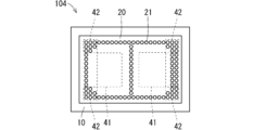
- FIG. 15 is a plan view showing the configuration of a circuit board 104 in embodiment 4.
- the metal plate 20 includes a high-density region 42 and a low-density region.
- the high-density region 42 is provided at the four corners of the metal plate 20.
- the low-density region corresponds to the region other than the high-density region 42.
- the density of the multiple recesses 21 in the low-density region is lower than the density of the multiple recesses 21 in the high-density region 42.
- the minimum distance Ds between adjacent recesses 21 and the width W of the recesses 21 are 0.2 mm or less.
- the areas where thermal stress is likely to concentrate are the four corners of the metal plate 20. In areas other than the four corners where thermal stress is small, the processing time for the recesses 21 can be shortened by reducing the density of the recesses 21.
- FIG. 16 is a plan view showing the configuration of a circuit board 105 in embodiment 5.
- the recess 21 in embodiment 5 is provided to surround not only the semiconductor element mounting area 41 but also the wiring bonding area 43.
- the wiring bonding area 43 is a predetermined area on the surface of the metal plate 20, and corresponds to the bonding portion where the metal plate 20 and the wiring 70 are bonded.
- the semiconductor device 201 in the fifth embodiment includes wiring 70 bonded to a wiring bonding area 43 on the surface of the metal plate 20.
- One end of the wiring 70 is bonded to the metal plate 20 via, for example, solder.
- the wiring 70 is electrically connected to the semiconductor element 40 via the solder and the metal plate 20.
- the other end of the wiring 70 is configured to be connectable to an external circuit (not shown).
- the wiring 70 is, for example, a metal plate processed into a predetermined shape.
- the recesses 21 are formed by a laser. By forming the recesses 21 by a laser, the processing time is shortened and the processing accuracy is improved.
- the laser used to process the recesses 21 is a UV laser or a green laser. By using a wavelength with a high optical absorption rate for Cu, the processing time for the recesses 21 is shortened.
- the resin part 50 is formed by transfer molding. This improves the filling of the resin into the recess 21, and improves the assembly of the semiconductor device 201.
Landscapes
- Structures Or Materials For Encapsulating Or Coating Semiconductor Devices Or Solid State Devices (AREA)
Priority Applications (2)
| Application Number | Priority Date | Filing Date | Title |
|---|---|---|---|
| PCT/JP2023/042326 WO2025115059A1 (ja) | 2023-11-27 | 2023-11-27 | 回路基板、半導体装置、回路基板の製造方法および半導体装置の製造方法 |
| JP2025560384A JPWO2025115059A1 (https=) | 2023-11-27 | 2023-11-27 |
Applications Claiming Priority (1)
| Application Number | Priority Date | Filing Date | Title |
|---|---|---|---|
| PCT/JP2023/042326 WO2025115059A1 (ja) | 2023-11-27 | 2023-11-27 | 回路基板、半導体装置、回路基板の製造方法および半導体装置の製造方法 |
Publications (1)
| Publication Number | Publication Date |
|---|---|
| WO2025115059A1 true WO2025115059A1 (ja) | 2025-06-05 |
Family
ID=95896453
Family Applications (1)
| Application Number | Title | Priority Date | Filing Date |
|---|---|---|---|
| PCT/JP2023/042326 Pending WO2025115059A1 (ja) | 2023-11-27 | 2023-11-27 | 回路基板、半導体装置、回路基板の製造方法および半導体装置の製造方法 |
Country Status (2)
| Country | Link |
|---|---|
| JP (1) | JPWO2025115059A1 (https=) |
| WO (1) | WO2025115059A1 (https=) |
Citations (9)
| Publication number | Priority date | Publication date | Assignee | Title |
|---|---|---|---|---|
| JP2011253950A (ja) * | 2010-06-02 | 2011-12-15 | Mitsubishi Electric Corp | 電力半導体装置 |
| JP2016029676A (ja) * | 2012-12-19 | 2016-03-03 | 富士電機株式会社 | 半導体装置 |
| JP2017188534A (ja) * | 2016-04-04 | 2017-10-12 | 株式会社デンソー | 電子装置及びその製造方法 |
| JP2018160653A (ja) * | 2017-03-22 | 2018-10-11 | 株式会社デンソー | 半導体装置 |
| WO2020050077A1 (ja) * | 2018-09-07 | 2020-03-12 | ローム株式会社 | 接合構造、半導体装置および接合構造の形成方法 |
| JP2022007599A (ja) * | 2020-06-26 | 2022-01-13 | 株式会社デンソー | 半導体装置 |
| JP2022062244A (ja) * | 2020-06-30 | 2022-04-19 | 富士電機株式会社 | 半導体モジュール |
| WO2023068096A1 (ja) * | 2021-10-22 | 2023-04-27 | 富士電機株式会社 | 半導体モジュール及び半導体モジュールの製造方法 |
| WO2023140042A1 (ja) * | 2022-01-20 | 2023-07-27 | ローム株式会社 | 半導体装置 |
-
2023
- 2023-11-27 JP JP2025560384A patent/JPWO2025115059A1/ja active Pending
- 2023-11-27 WO PCT/JP2023/042326 patent/WO2025115059A1/ja active Pending
Patent Citations (9)
| Publication number | Priority date | Publication date | Assignee | Title |
|---|---|---|---|---|
| JP2011253950A (ja) * | 2010-06-02 | 2011-12-15 | Mitsubishi Electric Corp | 電力半導体装置 |
| JP2016029676A (ja) * | 2012-12-19 | 2016-03-03 | 富士電機株式会社 | 半導体装置 |
| JP2017188534A (ja) * | 2016-04-04 | 2017-10-12 | 株式会社デンソー | 電子装置及びその製造方法 |
| JP2018160653A (ja) * | 2017-03-22 | 2018-10-11 | 株式会社デンソー | 半導体装置 |
| WO2020050077A1 (ja) * | 2018-09-07 | 2020-03-12 | ローム株式会社 | 接合構造、半導体装置および接合構造の形成方法 |
| JP2022007599A (ja) * | 2020-06-26 | 2022-01-13 | 株式会社デンソー | 半導体装置 |
| JP2022062244A (ja) * | 2020-06-30 | 2022-04-19 | 富士電機株式会社 | 半導体モジュール |
| WO2023068096A1 (ja) * | 2021-10-22 | 2023-04-27 | 富士電機株式会社 | 半導体モジュール及び半導体モジュールの製造方法 |
| WO2023140042A1 (ja) * | 2022-01-20 | 2023-07-27 | ローム株式会社 | 半導体装置 |
Also Published As
| Publication number | Publication date |
|---|---|
| JPWO2025115059A1 (https=) | 2025-06-05 |
Similar Documents
| Publication | Publication Date | Title |
|---|---|---|
| CN112166506B (zh) | 半导体装置 | |
| KR101391924B1 (ko) | 반도체 패키지 | |
| CN110383464B (zh) | 半导体装置 | |
| JP2014207430A (ja) | 半導体装置 | |
| KR19980024345A (ko) | 개량된 표면장착 고출력 반도체 패키지 및 그 제조방법 | |
| JP6724449B2 (ja) | 半導体装置および半導体装置の製造方法 | |
| CN103972277B (zh) | 半导体装置及其制造方法 | |
| US20200091025A1 (en) | Semiconductor device and method of manufacturing semiconductor device | |
| CN107527883A (zh) | 半导体装置及其制造方法以及导电柱 | |
| KR101569769B1 (ko) | 반도체 패키지 및 이를 위한 클립 구조체, 이의 제조 방법 | |
| CN111244061B (zh) | 氮化镓设备的封装结构 | |
| WO2025115059A1 (ja) | 回路基板、半導体装置、回路基板の製造方法および半導体装置の製造方法 | |
| KR20190054661A (ko) | 미세 음각 패턴이 형성된 기판 및 이를 포함하는 반도체 패키지 | |
| CN114566473A (zh) | 包括具有嵌入的封装式半导体芯片的引线框的印刷电路板 | |
| WO2022085043A1 (ja) | 半導体装置 | |
| JP7728236B2 (ja) | ベース板、半導体装置、ベース板の製造方法および半導体装置の製造方法 | |
| KR102603507B1 (ko) | 수직터미널단자를 구비한 반도체패키지 모듈 | |
| CN118398561A (zh) | 作为半导体本体的侧向边缘部分的应力释放结构 | |
| JP7480715B2 (ja) | 半導体装置 | |
| JP3203228B2 (ja) | 半導体装置とその製造方法 | |
| JP5261851B2 (ja) | 半導体装置の製造方法 | |
| WO2015079834A1 (ja) | 半導体装置 | |
| US20230307346A1 (en) | Semiconductor device and method of manufacturing the same | |
| CN110416178A (zh) | 一种集成电路封装结构及其封装方法 | |
| US20250167099A1 (en) | Semiconductor device and method for manufacturing thereof |
Legal Events
| Date | Code | Title | Description |
|---|---|---|---|
| 121 | Ep: the epo has been informed by wipo that ep was designated in this application |
Ref document number: 23960084 Country of ref document: EP Kind code of ref document: A1 |
|
| ENP | Entry into the national phase |
Ref document number: 2025560384 Country of ref document: JP Kind code of ref document: A |
|
| WWE | Wipo information: entry into national phase |
Ref document number: 2025560384 Country of ref document: JP |