WO2025069286A1 - ウエハ処理装置 - Google Patents
ウエハ処理装置 Download PDFInfo
- Publication number
- WO2025069286A1 WO2025069286A1 PCT/JP2023/035295 JP2023035295W WO2025069286A1 WO 2025069286 A1 WO2025069286 A1 WO 2025069286A1 JP 2023035295 W JP2023035295 W JP 2023035295W WO 2025069286 A1 WO2025069286 A1 WO 2025069286A1
- Authority
- WO
- WIPO (PCT)
- Prior art keywords
- wafer
- processing apparatus
- wafer processing
- processing chamber
- center
- Prior art date
- Legal status (The legal status is an assumption and is not a legal conclusion. Google has not performed a legal analysis and makes no representation as to the accuracy of the status listed.)
- Pending
Links
Images


Classifications
-
- H—ELECTRICITY
- H10—SEMICONDUCTOR DEVICES; ELECTRIC SOLID-STATE DEVICES NOT OTHERWISE PROVIDED FOR
- H10P—GENERIC PROCESSES OR APPARATUS FOR THE MANUFACTURE OR TREATMENT OF DEVICES COVERED BY CLASS H10
- H10P72/00—Handling or holding of wafers, substrates or devices during manufacture or treatment thereof
- H10P72/04—Apparatus for manufacture or treatment
- H10P72/0402—Apparatus for fluid treatment
- H10P72/0418—Apparatus for fluid treatment for etching
- H10P72/0421—Apparatus for fluid treatment for etching for drying etching
-
- C—CHEMISTRY; METALLURGY
- C23—COATING METALLIC MATERIAL; COATING MATERIAL WITH METALLIC MATERIAL; CHEMICAL SURFACE TREATMENT; DIFFUSION TREATMENT OF METALLIC MATERIAL; COATING BY VACUUM EVAPORATION, BY SPUTTERING, BY ION IMPLANTATION OR BY CHEMICAL VAPOUR DEPOSITION, IN GENERAL; INHIBITING CORROSION OF METALLIC MATERIAL OR INCRUSTATION IN GENERAL
- C23C—COATING METALLIC MATERIAL; COATING MATERIAL WITH METALLIC MATERIAL; SURFACE TREATMENT OF METALLIC MATERIAL BY DIFFUSION INTO THE SURFACE, BY CHEMICAL CONVERSION OR SUBSTITUTION; COATING BY VACUUM EVAPORATION, BY SPUTTERING, BY ION IMPLANTATION OR BY CHEMICAL VAPOUR DEPOSITION, IN GENERAL
- C23C16/00—Chemical coating by decomposition of gaseous compounds, without leaving reaction products of surface material in the coating, i.e. chemical vapour deposition [CVD] processes
- C23C16/02—Pretreatment of the material to be coated
- C23C16/0227—Pretreatment of the material to be coated by cleaning or etching
- C23C16/0236—Pretreatment of the material to be coated by cleaning or etching by etching with a reactive gas
-
- H—ELECTRICITY
- H10—SEMICONDUCTOR DEVICES; ELECTRIC SOLID-STATE DEVICES NOT OTHERWISE PROVIDED FOR
- H10P—GENERIC PROCESSES OR APPARATUS FOR THE MANUFACTURE OR TREATMENT OF DEVICES COVERED BY CLASS H10
- H10P50/00—Etching of wafers, substrates or parts of devices
-
- H—ELECTRICITY
- H10—SEMICONDUCTOR DEVICES; ELECTRIC SOLID-STATE DEVICES NOT OTHERWISE PROVIDED FOR
- H10P—GENERIC PROCESSES OR APPARATUS FOR THE MANUFACTURE OR TREATMENT OF DEVICES COVERED BY CLASS H10
- H10P50/00—Etching of wafers, substrates or parts of devices
- H10P50/20—Dry etching; Plasma etching; Reactive-ion etching
- H10P50/24—Dry etching; Plasma etching; Reactive-ion etching of semiconductor materials
- H10P50/242—Dry etching; Plasma etching; Reactive-ion etching of semiconductor materials of Group IV materials
-
- H—ELECTRICITY
- H10—SEMICONDUCTOR DEVICES; ELECTRIC SOLID-STATE DEVICES NOT OTHERWISE PROVIDED FOR
- H10P—GENERIC PROCESSES OR APPARATUS FOR THE MANUFACTURE OR TREATMENT OF DEVICES COVERED BY CLASS H10
- H10P72/00—Handling or holding of wafers, substrates or devices during manufacture or treatment thereof
- H10P72/04—Apparatus for manufacture or treatment
- H10P72/0431—Apparatus for thermal treatment
Definitions
- the present invention relates to a wafer processing device.
- Patent Document 1 As an example of a conventional technique for performing isotropic etching with high precision using dry processing, the adsorption/desorption etching method described in JP 2015-185594 A (Patent Document 1) is known.
- this conventional technique radicals generated by plasma are first adsorbed onto the surface of the layer to be etched of the object to be processed, which is placed on a stage placed inside the processing chamber, and a reaction layer is formed by a chemical reaction (adsorption process), and then thermal energy is applied to desorb and remove this reaction layer (desorption process).
- adsorption process chemical reaction
- thermal energy is applied to desorb and remove this reaction layer (desorption process).
- Etching is performed by alternately repeating this adsorption process and desorption process cyclically.
- a lamp that emits ultraviolet or infrared electromagnetic waves is provided above a stage placed inside the processing chamber to apply thermal energy to the surface of the workpiece during the desorption process.
- the workpiece is heated to a temperature at which the reactive layer on the surface of the layer to be etched sublimes in a short period of time.
- JP 2020-097060 A (Patent Document 2) describes a stage inside a processing chamber arranged inside a vacuum vessel, with ring-shaped IR lamps that irradiate electromagnetic waves in the infrared range (hereinafter referred to as infrared light or IR or IR light) arranged in multiple locations around a flow path directly above the stage through which reactive particles such as radicals are supplied into the processing chamber, and a reflector arranged above the IR lamps that reflects the IR light emitted from the IR lamps toward the top surface of a wafer stage in the processing chamber below or a wafer placed on that top surface.
- this conventional technology irradiates the wafer with IR light reflected by the reflector along with IR light directly emitted from the IR lamps, thereby heating the wafer in a short time.
- particles (etchant) constituting reactive gas or vapor supplied into the processing chamber inside the container are supplied downward from an inlet located in the center of the processing chamber, above the center of the top surface of the sample stage on which the wafer is placed and supported.
- the etchant comes into contact with and adheres to the top surface of the wafer, reacting with the surface of the film to be processed, which is a film structure having multiple film layers including the film layer to be processed that has been previously placed on the top surface of the wafer.
- the amount of reaction on the top surface of the wafer and its distribution of size are greatly affected by, for example, the balance between the amount of etchant supplied and the temperature of the reaction.
- the amount of etchant supplied varies depending largely on the flow path of the reactive gas or vapor. Therefore, in order to suppress variation in the amount of etchant in the radial or circumferential direction (in-plane direction) of the top surface of the wafer, it is desirable to have a configuration in which the etchant particles that reach the wafer move from the center of the wafer toward the outer periphery and then are exhausted from the space between the sample stage and the inner wall of the processing chamber surrounding it; specifically, a configuration in which the opening of the gas inlet, the center of the wafer, and the central axis in the vertical direction of the ring-shaped space located on the outer periphery of the sample stage coincide or are located at a position close to this (coaxial exhaust) is desirable.
- the above-mentioned conventional technology has this coaxial exhaust configuration.
- the object of the present invention is to provide a wafer processing device that improves processing accuracy and yield.
- a wafer processing apparatus comprising: a processing chamber arranged inside a vacuum vessel; a sample stage arranged in the lower center of the processing chamber on which a wafer to be processed is placed and supported; a gas inlet section arranged above the center of the upper surface of the sample stage and having a gas inlet port for introducing gas for processing the wafer into the processing chamber; and a lamp unit arranged around the gas inlet section and constituting the top surface of the processing chamber, the lamp unit comprising a ring-shaped plurality of lamps arranged in multiple layers around the gas inlet section and irradiating electromagnetic waves onto the wafer on the sample stage; and a reflecting member arranged in a ring shape around the gas inlet section above the plurality of lamps and having a reflecting surface configured to reflect the electromagnetic waves emitted from the plurality of lamps downward and toward a region toward the center of the processing chamber, the height of the reflecting surface being higher near the gas inlet section and lowering as it moves from the gas inlet section toward
- the present invention it is possible to reflect the electromagnetic waves emitted from the lamps upward in a specified direction, thereby changing the wafer temperature and its distribution as desired. This makes it possible to precisely keep the wafer temperature during processing within a range suitable for processing, improving processing yield.
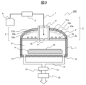
- FIG. 1 is a vertical cross-sectional view showing a schematic outline of the configuration of a wafer processing apparatus according to an embodiment of the present invention
- 2 is a vertical sectional view showing a schematic outline of the configuration of a wafer processing apparatus according to a modified example of the embodiment shown in FIG. 1.
- FIG. 3 is a longitudinal cross-sectional view showing a schematic outline of the configuration when the reflecting surfaces of multiple movable reflectors are parallel to the upper surface of the wafer in the modified example shown in Figure 2, and a graph showing the temperature distribution in the radial direction of the upper surface of the wafer in this case.
- FIG. 1 is a vertical cross-sectional view showing a schematic outline of the configuration of a wafer processing apparatus according to an embodiment of the present invention
- 2 is a vertical sectional view showing a schematic outline of the configuration of a wafer processing apparatus according to a modified example of the embodiment shown in FIG. 1.
- FIG. 3 is a longitudinal cross-sectional view showing a schematic outline of the configuration when the reflecting surfaces
- FIG. 3 is a longitudinal sectional view showing a schematic outline of a configuration in which the reflective surfaces of multiple movable reflectors are tilted with respect to the top surface of the wafer to reflect IR light toward the center of the wafer in the modified example shown in FIG. 2, and a graph showing the temperature distribution in the radial direction of the top surface of the wafer in this case.
- FIG. 3 is a graph showing an example of the change in intensity (illuminance) of direct IR light and reflected IR light at two IR lamps and a reflector and at a position on the wafer W below the two IR lamps and a reflector, as the inclination angle of the reflecting surface of the reflector changes in the modified example shown in FIG.
- FIG. 3 is a longitudinal sectional view showing a schematic outline of a configuration in which the reflective surfaces of multiple movable reflectors are tilted with respect to the top surface of the wafer to reflect IR light toward the center of the wafer in the modified example shown in FIG. 2, and a graph
- FIG. 6 is a diagram illustrating a model of the arrangement of IR lamp units used to calculate the example of the change in intensity of IR light shown in FIG. 5 .
- 3 is a graph showing an example of the distribution of IR light intensity (illuminance) in the radial direction of the upper surface of the wafer when the angle of the reflector shown in FIG. 2 is tilted by a predetermined value.
- FIG. 1 is a vertical cross-sectional view showing a schematic outline of the configuration of a wafer processing apparatus according to an embodiment of the present invention.
- the wafer processing apparatus 100 of this embodiment is roughly divided into a processing vessel whose interior can be depressurized, a gas supply unit connected to the top of the processing vessel to supply processing gas for processing a sample on a substrate such as a semiconductor wafer to be processed into the processing vessel, and an exhaust unit connected to the bottom of the processing vessel to exhaust gas from inside the processing vessel.
- the processing vessel is a vacuum vessel (not shown) connected to a transfer vessel through whose internal space the sample to be processed is transferred, and the side wall of the processing vessel is provided with an opening (gate) (not shown) that serves as a passageway for the sample to pass inside between the inside of the transfer vessel and the inside of the processing vessel.
- the processing vessel comprises a vacuum vessel 1 which is a metal vessel with a processing chamber 5 which is a cylindrical space inside, and a sample stage 4 which is located at the bottom inside the processing chamber 5 and on whose upper surface a wafer W which is the sample to be processed is placed and held or supported. Also, a gas introduction unit 6 is located above the center of the processing chamber 5 and through which processing, dilution or cleaning gas supplied to the processing chamber 5 flows in a pipe-like or cylindrical internal space. The gas introduction unit 6 is located above the center of the top surface of the processing chamber 5, and its lower end is exposed to the space inside the processing chamber 5, forming the top surface of the processing chamber 5.
- a dielectric gas inlet plate 10 having a disk shape is disposed at the lower end of the gas inlet unit 6.
- At least one gas inlet port 11 is disposed at the center of the gas inlet plate 10, through which gas such as a processing gas that has passed through a cylindrical space inside the gas inlet unit 6 is introduced toward the processing chamber 5 through the inside.
- particles of the processing gas that enter the processing chamber 5 through the gas inlet port 11 diffuse inside the processing chamber 5 and adhere to a film structure having multiple layers including a film layer to be processed and a film layer for a mask, which are disposed in advance on the upper surface of the wafer W placed on the upper surface of the sample stage 4, and the adhered gas particles interact or react with the material on the surface of the film layer to be processed to form the desired product.
- a lamp unit 2 which constitutes the upper part of the vacuum vessel 1 and is arranged above the processing chamber 5 and surrounding the outer periphery of the gas introduction unit 6.
- the lamp unit 2 in this example is a lamp that can irradiate infrared light (IR light) into the inside of the processing chamber 5 to heat the wafer W placed on the upper surface of the sample stage 4, and has multiple (three in this figure) concentrically arranged IR lamps 2a surrounding the outer periphery of the gas introduction unit 6.
- the lamp unit 2 is a flat ring-shaped member made of a material that can transmit IR light, and has a transmission window 2b that constitutes the top surface of the processing chamber 5 around the lower end of the gas introduction unit 6.
- the lamp unit 2 in this example is provided with a cover dome 3 above the IR lamp 2a, which is a plate-like member arranged to surround the outer periphery of the gas introduction unit 6 and cover the IR lamp 2a and the transmission window 2b, and has a curved shape with a high central position and a low outer periphery.
- the cover dome 3 has a circular opening in the center and has a ring-like shape when viewed from above, and its inner peripheral edge is arranged to surround the outer periphery of the gas introduction unit 6.
- the outer surface and lower surface (inner surface) of the cover dome 3 are inclined so that they become lower from the center toward the outer periphery, and the angle of inclination increases from the center to the outer periphery, giving it a so-called dome-like shape.
- the inner surface of the cover dome 3 has such a shape, and is configured to function as a reflective surface that reflects the IR light emitted from the IR lamps 2a.
- a reflective surface that reflects the IR light emitted from the IR lamps 2a.
- the IR light (IR reflected light) emitted from each IR lamp 2a and reflected by the inner wall surface of the cover dome 3 travels downward and toward the center of the upper surface of the stage 4, passes through the gaps between the multiple IR lamps 2a arranged in a ring shape and the gap between the gas introduction unit 6, and is irradiated onto the surface of the center side of the wafer W when the wafer W is placed above the upper surface of the sample stage 4.
- each IR lamp 2a the IR light emitted upward from each IR lamp 2a is reflected by the inner surface of the cover dome 3 and irradiated onto the wafer W through a space closer to the center of the wafer W than each IR lamp 2a.
- the central area on the top surface of the wafer W is irradiated with more IR reflected light than the outer periphery area, resulting in a greater intensity or amount of IR light being irradiated.
- FIG. 2 is a vertical cross-sectional view showing a schematic outline of the configuration of a wafer processing apparatus according to a modified example of the embodiment shown in FIG. 1. The difference between the embodiment shown in FIG.
- the reflector units 21, 22, and 23 are made up of multiple rectangular flat plate members, and have multiple reflectors 21a, 21b, ..., 22a, 22b, ..., 23a, 23b, ... that have surfaces (reflecting surfaces) capable of reflecting IR light.
- the multiple reflectors 21a, 21b, ..., 22a, 22b, ..., 23a, 23b, ... are arranged in a ring shape on a circumference at three different heights from the top surface of the wafer W, at three radial positions of different lengths from the center.
- the surface (top surface) opposite the reflective surface of each of the multiple reflectors 21a, 21b, ..., 22a, 22b, ..., 23a, 23b, ... is connected to an angle adjustment mechanism arranged on the underside (inside) of the underside of the cover dome 3', so that the reflective surface of the IR light from the IR lamp 2a can be tilted toward the center of the processing chamber 5, the sample stage 4, or the wafer W.
- the central points of the reflective surfaces of the reflectors 21a, 21b, ..., 22a, 22b, ..., 23a, 23b, ... that constitute each of the reflector units 21, 22, 23 as a plurality of groups are arranged at positions where the radius from the central axis of the wafer W or stage 4 or processing chamber 5 for each reflector unit matches or is close enough to be regarded as the radius of each of the three IR lamps 2a arranged in a ring shape. Furthermore, the height from the top surface of the wafer W at which the central points of the reflective surfaces of the reflectors belonging to each of these three reflector units 21 to 23 are arranged increases for each group of reflectors as they approach the center of the processing chamber 5 or sample stage 4 or wafer W. In other words, the central positions of the reflectors 21a, 21b, ... are arranged at the highest position from the wafer W, and the vertical distance from the IR lamp 2a is also the greatest.
- each reflector unit 21, 22, 23 when the reflecting surfaces of the reflectors 21a, 21b, ..., 22a, 22b, ..., 23a, 23b, ... of each reflector unit 21, 22, 23 are held at a predetermined angle so that the reflected IR light (IR reflected light) is directed toward the center of the processing chamber 5 or stage 4, or the top surface of the wafer W, the reflected IR light (IR reflected light) travels downward toward the center of the top surface of the wafer W, passing through the gaps between the multiple ring-shaped IR lamps 2a and the gaps between the gas introduction unit 6, and is irradiated onto the top surface of the wafer W.
- each IR lamp 2a the IR light emitted upward from each IR lamp 2a is reflected by each reflector unit 21, 22, 23, and is irradiated onto the wafer W through a space closer to the center of the wafer W than each IR lamp 2a.
- the IR light direct IR light
- more IR reflected light is irradiated than in the outer peripheral area, resulting in IR light of greater intensity.
- the top surface of the wafer W is irradiated with both reflected IR light and direct IR light, as in the above case.
- the intensity of the reflected IR light irradiated to the central area of the wafer W is relatively small compared to when the reflectors of the reflector units 21, 22, and 23 are tilted so that the reflected IR light is directed toward the center.
- the lower end of the gas introduction unit 6 forms the center of the ceiling of the processing chamber 5, and it is not possible to irradiate with the strong intensity obtained by placing an IR lamp above the center and irradiating the wafer W with the direct IR light from the IR lamp 2a at an angle perpendicular to or close to the top surface of the wafer W. Therefore, the intensity and amount of the direct IR light are also relatively small compared to that irradiated to the outer periphery.
- Figure 3 is a graph showing a schematic example of the temperature distribution on the wafer obtained when the reflective surface of the reflector of the modified example shown in Figure 2 is held parallel to the sample stage or wafer.
- the direct IR light is indicated by a solid arrow
- the reflected IR light is indicated by a dashed arrow.
- the direct IR light emitted downward from the lamp unit 2 is directly irradiated from the IR lamp 2a to the upper surface of the wafer W arranged below.
- the IR light emitted upward from the IR lamp 2a becomes IR reflected light that is reflected downward by the reflective surface of the reflector of any of the reflector units 21 to 23, passes through the gap between the IR lamps 2a that have a ring shape arranged in three concentric layers, and is irradiated to the upper surface of the wafer W below the gap.
- the intensity or amount of direct IR light and reflected IR light emitted from the lamp unit 2 is greater in the outer peripheral region compared to the central region of the wafer W.
- the temperature of the top surface of the wafer W is relatively lower in the central region and higher in the outer peripheral region.
- Figure 4 is a graph showing a schematic example of the temperature distribution on the wafer obtained when the reflective surface of the reflector of the modified example shown in Figure 2 is held toward the center of the sample stage or wafer.
- the direct IR light is indicated by a solid arrow
- the reflected IR light is indicated by a dashed arrow.
- the direct IR light emitted downward from the lamp unit 2 is directly irradiated from the IR lamp 2a to the upper surface of the wafer W arranged below.
- the IR light emitted upward from the IR lamp 2a becomes IR reflected light reflected downward and toward the center of the wafer W by the reflective surface of the reflector of any of the reflector units 21 to 23, passes through the gap between the IR lamps 2a having a ring shape arranged in three concentric layers, and is irradiated to the upper surface of the wafer W below the gap.
- the IR light emitted upward from the IR lamp 2a-1 arranged on the innermost circumference is reflected downward toward the central region of the wafer W by the reflectors 21a, 21b, ..., and the IR reflected light passes through the gap between the innermost IR lamp 2a-1 and the outer periphery of the lower end of the gas introduction unit 6, and further travels toward the center of the wafer W and is irradiated onto the upper surface of the wafer W.
- the lower end of the cylindrical side wall of the gas introduction unit 6 or the gas introduction plate 10 may be made of a material that transmits IR light, in which case the IR reflected light reflected by at least one of the reflector units 21 to 23 passes through the gas introduction unit 6 that constitutes the center of the top surface of the processing chamber 5 and is irradiated with a greater intensity or amount to the center of the wafer W, where the intensity or amount of direct IR light is small.
- the intensity or amount of reflected IR light is greater in the central region of the wafer W compared to the peripheral region, and the temperature of the top surface of the wafer W is relatively higher in the central region and lower in the peripheral region.
- Figures 5 and 6 an example of the change in the intensity (illuminance) of the direct IR light and reflected IR light from the IR lamp 2a as a function of the inclination of the reflecting surface of the reflector of the lamp unit 2 in the modified example shown in Figure 2 will be described.
- Figure 5 is a graph showing an example of the change in the intensity (illuminance) of the direct IR light and reflected IR light at the two IR lamps and the reflector and the position on the wafer W below it, as the inclination angle of the reflector's reflecting surface changes in the modified example shown in Figure 2.
- Figure 6 is a graph showing an example of the distribution of the intensity (illuminance) of IR light in the radial direction of the top surface of the wafer when the angle of the reflector shown in Figure 2 is parallel to the wafer and when the angle of the reflector's reflecting surface is inclined by a predetermined value.
- Figures 5 and 7 a model was used in which conditions including the arrangement of the lamp unit 2 and the wafer W and their relative positional relationship were appropriately set, and the change in the intensity of the IR light was calculated under these conditions.
- Figure 6 is a schematic diagram showing a model of the arrangement of the IR lamp unit used to calculate an example of the change in the intensity of the IR light shown in Figure 5.
- two IR lamps 2a-1, 2a-2 are arranged above the wafer W at a height (distance) d1 above the top surface of the wafer W, spaced apart by a distance L in the horizontal direction (left-right direction in the figure). Also, above each of these IR lamps 2a-1, 2a-2, reflectors 21a, 22a are arranged at a distance (height) d2.
- the IR lamp 2a-1 on the left side of the figure is the innermost lamp in the radial direction from the center of the processing chamber 5 among the IR lamps 2a arranged in the triple ring shape in FIG. 2, and the IR lamp 2a-2 on the right side of the figure is the second lamp in the radial direction.
- the reflectors 21a, 22a located above these belong to the reflector units 21, 22, respectively.
- the distance between points A and B on the wafer W projected vertically downward from above is defined as L.
- the reflector 21a holds its reflective surface parallel to the wafer W, and the reflector 22a tilts its reflective surface at an angle ⁇ relative to the horizontal direction (plane) while changing the angle within a specified range.
- the total intensity of the IR direct light from the IR lamps 2a-1, 2a-2 and the IR reflected light from the reflectors 21a, 22a at point (position) X where the IR reflected light emitted directly upward from the IR lamp 2a-2 and reflected by the reflector 22a is irradiated onto the wafer W is calculated.
- reference numeral 502 indicates the change in the total intensity of the direct IR light from the IR lamps 2a-1 and 2a-2
- reference numeral 503 indicates the change in the total intensity of the reflected IR light from the reflectors 21a and 22a
- reference numeral 501 indicates the change in the sum of the total intensity of the direct IR light 502 and the total intensity of the reflected IR light 503.
- the calculations were performed with the distance L as an arbitrary unit of size set to 5, the height d1 set to 5, and the height d2 set to 0.1.
- the example of this figure shows that the intensity 501 of the IR light is maximum under the condition that the tilt angle of the reflector 22a is small when the position X is located between the positions A and B in FIG. 6.
- FIG. 7 shows the change in IR light intensity with respect to the change in distance from the center of the wafer W when an IR lamp 2a and a reflector above it are placed above a specific position in the radial direction from the center of the wafer W and the angle of the reflecting surface is set to a specified value.
- the IR lamp 2a is placed at the distance position at the right end of the graph
- reference numeral 602 indicates the change in intensity of direct IR light from the IR lamp 2a
- reference numeral 603 indicates the change in intensity of reflected IR light from the reflector above the IR lamp 2a
- reference numeral 601 indicates the change in the sum of the intensity 602 of direct IR light and the intensity 603 of reflected IR light. It can be seen from this figure that the intensity 602 of direct IR light and the intensity 603 of reflected IR light increase as the radial position from the center of the wafer W approaches the point projected from above by the IR lamp 2a.
- the temperature value and its distribution of the wafer W can be made as desired, including so-called high in the middle and high on the outside.
- the angle adjustment mechanism to which each reflector of the reflector units 21 to 23 is attached has the function of changing the angle at which the reflecting surface faces the center or central area of the wafer W or stage 4 or processing chamber 5 to an angle facing the outer peripheral area of these, for example, the inner peripheral side wall of the processing chamber 5, and each of the reflector units 21 to 23 can be adjusted independently to a different angle.
- the angles of the reflector units 21 to 23 are detected by a control unit that issues command signals to control the operation of each part of the wafer processing apparatus 100, 200 (not shown in Figures 1 and 2) by receiving outputs from multiple temperature sensors arranged inside the stage 4, and are adjusted by sending a signal to the angle adjustment mechanism depending on whether the temperature value or distribution of the wafer W is different from the target value.
- a greater intensity or amount of reflected IR light is supplied from the lamp unit 2 to the center side of the wafer, or the angle of the lamp unit 2 is appropriately adjusted to irradiate the desired area of the wafer W with the IR reflected light reflected by each reflector of the reflector units 21, 22, and 23, thereby obtaining the temperature value and its distribution during processing of the wafer W suitable for processing. This improves the processing accuracy and yield of the wafer W processed in the wafer processing apparatuses 100 and 200.
Landscapes
- Chemical & Material Sciences (AREA)
- Engineering & Computer Science (AREA)
- General Chemical & Material Sciences (AREA)
- Chemical Kinetics & Catalysis (AREA)
- Materials Engineering (AREA)
- Mechanical Engineering (AREA)
- Metallurgy (AREA)
- Organic Chemistry (AREA)
- Physics & Mathematics (AREA)
- Plasma & Fusion (AREA)
- Drying Of Semiconductors (AREA)
- Container, Conveyance, Adherence, Positioning, Of Wafer (AREA)
Priority Applications (5)
| Application Number | Priority Date | Filing Date | Title |
|---|---|---|---|
| PCT/JP2023/035295 WO2025069286A1 (ja) | 2023-09-27 | 2023-09-27 | ウエハ処理装置 |
| JP2025508420A JPWO2025069286A1 (https=) | 2023-09-27 | 2023-09-27 | |
| KR1020257005042A KR20250048007A (ko) | 2023-09-27 | 2023-09-27 | 웨이퍼 처리 장치 |
| CN202380064370.9A CN120051852A (zh) | 2023-09-27 | 2023-09-27 | 晶片处理装置 |
| TW113135763A TWI907078B (zh) | 2023-09-27 | 2024-09-20 | 晶圓處理裝置 |
Applications Claiming Priority (1)
| Application Number | Priority Date | Filing Date | Title |
|---|---|---|---|
| PCT/JP2023/035295 WO2025069286A1 (ja) | 2023-09-27 | 2023-09-27 | ウエハ処理装置 |
Publications (1)
| Publication Number | Publication Date |
|---|---|
| WO2025069286A1 true WO2025069286A1 (ja) | 2025-04-03 |
Family
ID=95202375
Family Applications (1)
| Application Number | Title | Priority Date | Filing Date |
|---|---|---|---|
| PCT/JP2023/035295 Pending WO2025069286A1 (ja) | 2023-09-27 | 2023-09-27 | ウエハ処理装置 |
Country Status (5)
| Country | Link |
|---|---|
| JP (1) | JPWO2025069286A1 (https=) |
| KR (1) | KR20250048007A (https=) |
| CN (1) | CN120051852A (https=) |
| TW (1) | TWI907078B (https=) |
| WO (1) | WO2025069286A1 (https=) |
Citations (9)
| Publication number | Priority date | Publication date | Assignee | Title |
|---|---|---|---|---|
| JPS647519A (en) * | 1987-06-30 | 1989-01-11 | Oki Electric Ind Co Ltd | Annealing device |
| JPH0992624A (ja) * | 1995-09-25 | 1997-04-04 | Semitsukusu Eng Kk | 熱処理炉 |
| JPH09167742A (ja) * | 1995-12-14 | 1997-06-24 | Shin Etsu Handotai Co Ltd | 加熱炉 |
| JPH10321546A (ja) * | 1997-05-22 | 1998-12-04 | Kokusai Electric Co Ltd | 熱処理炉 |
| JP2006147943A (ja) * | 2004-11-22 | 2006-06-08 | Kokusai Electric Semiconductor Service Inc | 基板処理装置及び半導体装置の製造方法 |
| JP2009088348A (ja) * | 2007-10-01 | 2009-04-23 | Hitachi Kokusai Electric Inc | 半導体製造装置 |
| JP2009200330A (ja) * | 2008-02-22 | 2009-09-03 | Denso Corp | 半導体製造装置 |
| JP2011176128A (ja) * | 2010-02-24 | 2011-09-08 | Toshiba Corp | 半導体製造装置及び半導体装置の製造方法 |
| JP2018181925A (ja) * | 2017-04-05 | 2018-11-15 | ウシオ電機株式会社 | 加熱光源装置 |
Family Cites Families (4)
| Publication number | Priority date | Publication date | Assignee | Title |
|---|---|---|---|---|
| US6080965A (en) * | 1997-09-18 | 2000-06-27 | Tokyo Electron Limited | Single-substrate-heat-treatment apparatus in semiconductor processing system |
| JP2015185594A (ja) | 2014-03-20 | 2015-10-22 | 株式会社日立ハイテクノロジーズ | エッチング装置 |
| JP2020097060A (ja) | 2017-03-31 | 2020-06-25 | 日本電産株式会社 | ロボット教示装置、ロボット教示装置の制御方法及びロボット教示プログラム |
| US12051574B2 (en) * | 2019-12-20 | 2024-07-30 | Hitachi High-Tech Corporation | Wafer processing method and plasma processing apparatus |
-
2023
- 2023-09-27 WO PCT/JP2023/035295 patent/WO2025069286A1/ja active Pending
- 2023-09-27 JP JP2025508420A patent/JPWO2025069286A1/ja active Pending
- 2023-09-27 KR KR1020257005042A patent/KR20250048007A/ko active Pending
- 2023-09-27 CN CN202380064370.9A patent/CN120051852A/zh active Pending
-
2024
- 2024-09-20 TW TW113135763A patent/TWI907078B/zh active
Patent Citations (9)
| Publication number | Priority date | Publication date | Assignee | Title |
|---|---|---|---|---|
| JPS647519A (en) * | 1987-06-30 | 1989-01-11 | Oki Electric Ind Co Ltd | Annealing device |
| JPH0992624A (ja) * | 1995-09-25 | 1997-04-04 | Semitsukusu Eng Kk | 熱処理炉 |
| JPH09167742A (ja) * | 1995-12-14 | 1997-06-24 | Shin Etsu Handotai Co Ltd | 加熱炉 |
| JPH10321546A (ja) * | 1997-05-22 | 1998-12-04 | Kokusai Electric Co Ltd | 熱処理炉 |
| JP2006147943A (ja) * | 2004-11-22 | 2006-06-08 | Kokusai Electric Semiconductor Service Inc | 基板処理装置及び半導体装置の製造方法 |
| JP2009088348A (ja) * | 2007-10-01 | 2009-04-23 | Hitachi Kokusai Electric Inc | 半導体製造装置 |
| JP2009200330A (ja) * | 2008-02-22 | 2009-09-03 | Denso Corp | 半導体製造装置 |
| JP2011176128A (ja) * | 2010-02-24 | 2011-09-08 | Toshiba Corp | 半導体製造装置及び半導体装置の製造方法 |
| JP2018181925A (ja) * | 2017-04-05 | 2018-11-15 | ウシオ電機株式会社 | 加熱光源装置 |
Also Published As
| Publication number | Publication date |
|---|---|
| TWI907078B (zh) | 2025-12-01 |
| TW202514862A (zh) | 2025-04-01 |
| CN120051852A (zh) | 2025-05-27 |
| JPWO2025069286A1 (https=) | 2025-04-03 |
| KR20250048007A (ko) | 2025-04-07 |
Similar Documents
| Publication | Publication Date | Title |
|---|---|---|
| US11043403B2 (en) | Substrate support unit and substrate processing apparatus having the same including reflective member configured to reflect light toward substrate | |
| KR101819095B1 (ko) | Epi 프로세스를 위한 균일성 튜닝 렌즈를 갖는 서셉터 지지 샤프트 | |
| JP6625891B2 (ja) | 真空処理装置 | |
| KR20190079473A (ko) | 웨이퍼 처리 방법 및 웨이퍼 처리 장치 | |
| US9790597B2 (en) | Substrate processing apparatus, substrate processing method and storage medium | |
| TW201625824A (zh) | 處理腔室 | |
| TWI793441B (zh) | 電漿處理裝置及晶圓處理方法 | |
| JP7387794B2 (ja) | 遠隔プラズマ酸化チャンバ用ドッグボーン入口錐体輪郭 | |
| KR20190022912A (ko) | 에피 균일성 조정을 개선하기 위한 가열 변조기 | |
| WO2025069286A1 (ja) | ウエハ処理装置 | |
| US6879777B2 (en) | Localized heating of substrates using optics | |
| KR102846377B1 (ko) | 진공 처리 장치 및 기울기 조정 방법 | |
| JP2011204819A (ja) | 基板処理装置及び基板処理方法 | |
| JP7452992B2 (ja) | プラズマ処理装置およびプラズマ処理装置の運転方法 | |
| KR20250038662A (ko) | 웨이퍼 처리 장치 | |
| CN103715051B (zh) | 等离子体处理装置及方法 | |
| KR20210029671A (ko) | 기판 처리 장치 및 기판 처리 방법 | |
| US20150163860A1 (en) | Apparatus and method for uniform irradiation using secondary irradiant energy from a single light source | |
| TW202529227A (zh) | 半導體製程設備及其控制方法 | |
| TWI691030B (zh) | 用於燈泡加熱組件的散光器 | |
| TWI909686B (zh) | 具有用於限制等離子體的擋板的等離子體處理裝置 | |
| CN111627844A (zh) | 新型边缘刻蚀反应装置和边缘刻蚀方法 | |
| JP7619734B2 (ja) | 基板処理装置 | |
| CN223321237U (zh) | 一种加热结构及半导体处理设备 | |
| CN223282957U (zh) | 一种灯箱结构 |
Legal Events
| Date | Code | Title | Description |
|---|---|---|---|
| ENP | Entry into the national phase |
Ref document number: 2025508420 Country of ref document: JP Kind code of ref document: A |
|
| WWE | Wipo information: entry into national phase |
Ref document number: 2025508420 Country of ref document: JP |
|
| ENP | Entry into the national phase |
Ref document number: 20257005042 Country of ref document: KR Kind code of ref document: A |
|
| WWE | Wipo information: entry into national phase |
Ref document number: 202380064370.9 Country of ref document: CN |
|
| WWP | Wipo information: published in national office |
Ref document number: 1020257005042 Country of ref document: KR |
|
| 121 | Ep: the epo has been informed by wipo that ep was designated in this application |
Ref document number: 23954262 Country of ref document: EP Kind code of ref document: A1 |
|
| WWP | Wipo information: published in national office |
Ref document number: 202380064370.9 Country of ref document: CN |