WO2025052920A1 - 受動電子部品 - Google Patents
受動電子部品 Download PDFInfo
- Publication number
- WO2025052920A1 WO2025052920A1 PCT/JP2024/029567 JP2024029567W WO2025052920A1 WO 2025052920 A1 WO2025052920 A1 WO 2025052920A1 JP 2024029567 W JP2024029567 W JP 2024029567W WO 2025052920 A1 WO2025052920 A1 WO 2025052920A1
- Authority
- WO
- WIPO (PCT)
- Prior art keywords
- internal electrode
- layer
- electrode layer
- electronic component
- capacitor
- Prior art date
- Legal status (The legal status is an assumption and is not a legal conclusion. Google has not performed a legal analysis and makes no representation as to the accuracy of the status listed.)
- Pending
Links
Images


Classifications
-
- H—ELECTRICITY
- H01—ELECTRIC ELEMENTS
- H01G—CAPACITORS; CAPACITORS, RECTIFIERS, DETECTORS, SWITCHING DEVICES, LIGHT-SENSITIVE OR TEMPERATURE-SENSITIVE DEVICES OF THE ELECTROLYTIC TYPE
- H01G4/00—Fixed capacitors; Processes of their manufacture
- H01G4/30—Stacked capacitors
-
- H—ELECTRICITY
- H01—ELECTRIC ELEMENTS
- H01G—CAPACITORS; CAPACITORS, RECTIFIERS, DETECTORS, SWITCHING DEVICES, LIGHT-SENSITIVE OR TEMPERATURE-SENSITIVE DEVICES OF THE ELECTROLYTIC TYPE
- H01G4/00—Fixed capacitors; Processes of their manufacture
- H01G4/33—Thin- or thick-film capacitors (thin- or thick-film circuits; capacitors without a potential-jump or surface barrier specially adapted for integrated circuits, details thereof, multistep manufacturing processes therefor)
-
- H—ELECTRICITY
- H01—ELECTRIC ELEMENTS
- H01G—CAPACITORS; CAPACITORS, RECTIFIERS, DETECTORS, SWITCHING DEVICES, LIGHT-SENSITIVE OR TEMPERATURE-SENSITIVE DEVICES OF THE ELECTROLYTIC TYPE
- H01G4/00—Fixed capacitors; Processes of their manufacture
- H01G4/38—Multiple capacitors, i.e. structural combinations of fixed capacitors
-
- H—ELECTRICITY
- H01—ELECTRIC ELEMENTS
- H01G—CAPACITORS; CAPACITORS, RECTIFIERS, DETECTORS, SWITCHING DEVICES, LIGHT-SENSITIVE OR TEMPERATURE-SENSITIVE DEVICES OF THE ELECTROLYTIC TYPE
- H01G4/00—Fixed capacitors; Processes of their manufacture
- H01G4/40—Structural combinations of fixed capacitors with other electric elements, the structure mainly consisting of a capacitor, e.g. RC combinations
Definitions
- the present invention relates to passive electronic components.
- Patent document 1 discloses an electronic component having a plurality of conductor layers stacked on a substrate, the electronic component having a first capacitor formed by two of the plurality of conductor layers adjacent in the stacking direction and a dielectric film located between them, and a second capacitor formed by two of the plurality of conductor layers adjacent in the stacking direction and a dielectric film located between them, the electronic component being characterized in that the thicknesses of the dielectric film constituting the first capacitor and the dielectric film constituting the second capacitor are different from each other.
- the electronic component described in Patent Document 1 for example, electronic component 1 described in FIG. 2 of Patent Document 1, has a plurality of capacitors, including a first capacitor formed of conductor pattern 25, first dielectric film 4, and conductor pattern 31, a second capacitor formed of conductor pattern 26, second dielectric film 5, and conductor pattern 32, and a third capacitor formed of conductor pattern 25, first dielectric film 4, second dielectric film 5, and conductor pattern 33.
- the first dielectric film 4 formed in advance on the conductor pattern 26 is removed by patterning to expose the conductor pattern 26, as shown in FIG. 9 of Patent Document 1.
- an impurity layer such as a metal oxide layer or a metal fluoride layer is formed on the surface of the conductor pattern 26.
- the conductor pattern 31 is formed on the first region 25A of the conductor pattern 25 via the first dielectric film 4.
- the conductor pattern 31 is made of a laminate of a seed layer S and a plating layer P.
- the seed layer S is first formed on the entire surface of the first dielectric film 4, and then a resist layer is patterned on the seed layer S so that the seed layer S in the region where the conductor pattern 31 is to be formed (the region overlapping the first region 25A of the conductor pattern 25) is exposed.
- the seed layer S is once formed on the first dielectric film 4 on which the conductor pattern 31 is not formed, for example, on the first dielectric film 4 covering the second region 25B of the conductor pattern 25, and then the seed layer S is removed.
- an impurity layer is formed on the surface of the first dielectric film 4 covering the second region 25B of the conductor pattern 25 due to process damage when removing the seed layer S.
- the second dielectric film 5 and the conductor pattern 33 are formed in order on the first dielectric film 4 in a state in which an impurity layer is formed on the surface of the first dielectric film 4 covering the second region 25B of the conductor pattern 25, as shown in Figures 11 and 12 of Patent Document 1, in the obtained third capacitor, the dielectric loss tangent of the impurity layer formed on the surface of the first dielectric film 4 becomes large. Therefore, in the electronic component 1 described in Figure 2 of Patent Document 1, the power loss in the third capacitor becomes large, and as a result, it is not possible to exhibit electrical performance with excellent high-frequency characteristics.
- Patent Document 1 As described above, there is room for improvement in the electronic component described in Patent Document 1 in terms of being able to achieve electrical performance with excellent high-frequency characteristics in a configuration with multiple capacitors.
- the present invention has been made to solve the above problems, and aims to provide a passive electronic component that has a configuration with multiple capacitors and can exhibit electrical performance with excellent high-frequency characteristics.
- the passive electronic component of the present invention comprises a substrate having a first main surface and a second main surface facing each other in a first direction, and a plurality of capacitors provided on the first main surface side of the substrate, the plurality of capacitors including a first capacitor and a second capacitor spaced apart from the first capacitor in a second direction perpendicular to the first direction, the first capacitor having a first capacitance forming portion including a first internal electrode layer, a first dielectric layer, and a second internal electrode layer stacked in order from the substrate side in the first direction, the second capacitor having a second capacitance forming portion including a third internal electrode layer, a second dielectric layer, and a fourth internal electrode layer stacked in order from the substrate side in the first direction, and at least a portion of the second internal electrode layer and at least a portion of the third internal electrode layer are in contact with the surface of the first dielectric layer opposite the substrate.
- the present invention provides a passive electronic component that has multiple capacitors and exhibits excellent electrical performance with high-frequency characteristics.
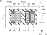
- FIG. 1 is a plan view showing an example of a passive electronic component according to a first embodiment of the present invention.
- FIG. 2 is a schematic cross-sectional view showing an example of a cross section of the passive electronic component shown in FIG. 1 taken along line a1-a2.
- FIG. 3 is a schematic cross-sectional view showing a step of preparing a substrate in an example of the method for manufacturing a passive electronic component according to the first embodiment of the present invention.
- FIG. 4 is a schematic cross-sectional view showing a step of forming an insulating layer in an example of a method for manufacturing a passive electronic component according to the first embodiment of the present invention.
- FIG. 1 is a plan view showing an example of a passive electronic component according to a first embodiment of the present invention.
- FIG. 2 is a schematic cross-sectional view showing an example of a cross section of the passive electronic component shown in FIG. 1 taken along line a1-a2.
- FIG. 3 is a schematic cross-sectional view showing a
- FIG. 5 is a schematic cross-sectional view showing a step of forming a first internal electrode layer in an example of a method for manufacturing a passive electronic component according to the first embodiment of the present invention.
- FIG. 6 is a schematic cross-sectional view showing a step of forming a first dielectric layer in an example of a method for manufacturing a passive electronic component according to the first embodiment of the present invention.
- FIG. 7 is a schematic cross-sectional view showing a step of forming a second internal electrode layer and a third internal electrode layer in an example of a method for manufacturing a passive electronic component according to the first embodiment of the present invention.
- FIG. 6 is a schematic cross-sectional view showing a step of forming a first dielectric layer in an example of a method for manufacturing a passive electronic component according to the first embodiment of the present invention.
- FIG. 7 is a schematic cross-sectional view showing a step of forming a second internal electrode layer and a third internal electrode layer in an example of a method for manufacturing a
- FIG. 8 is a schematic cross-sectional view showing a step of forming a second dielectric layer in an example of a method for manufacturing a passive electronic component according to the first embodiment of the present invention.
- FIG. 9 is a schematic cross-sectional view showing a step of forming a fourth internal electrode layer in an example of a method for manufacturing a passive electronic component according to the first embodiment of the present invention.
- FIG. 10 is a schematic cross-sectional view showing a step of forming a moisture-resistant protective layer in an example of a method for manufacturing a passive electronic component according to the first embodiment of the present invention.
- FIG. 11 is a schematic cross-sectional view showing a step of forming a resin protective layer in an example of a method for manufacturing a passive electronic component according to the first embodiment of the present invention.
- FIG. 12 is a schematic cross-sectional view showing a step of forming a first external electrode, a second external electrode, a third external electrode, and a fourth external electrode in an example of a method for manufacturing a passive electronic component according to the first embodiment of the present invention.
- FIG. 13 is a schematic plan view showing another example of the passive electronic component according to the first embodiment of the present invention.
- FIG. 14 is a schematic cross-sectional view showing an example of a cross section of the passive electronic component shown in FIG. 13 taken along line a3-a4.
- FIG. 15 is a plan view schematic diagram showing an example of a passive electronic component according to the second embodiment of the present invention.
- FIG. 16 is a schematic cross-sectional view showing an example of a cross section of the passive electronic component shown in FIG. 15 taken along line segment b1-b2.
- FIG. 17 is a schematic plan view showing another example of the passive electronic component according to the second embodiment of the present invention.
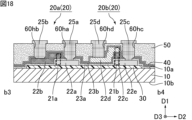
- FIG. 18 is a schematic cross-sectional view showing an example of a cross section of the passive electronic component shown in FIG. 17 taken along line segment b3-b4.
- FIG. 19 is an equivalent circuit diagram showing an example of a passive electronic component according to the third embodiment of the present invention.
- FIG. 20 is a plan view schematic diagram showing an example of a passive electronic component according to the third embodiment of the present invention.
- FIG. 21 is a schematic cross-sectional view showing an example of a cross section of the passive electronic component shown in FIG. 20 taken along line c1-c2.
- FIG. 22 is a schematic cross-sectional view showing an example of a cross section of the passive electronic component shown in FIG. 20 taken along line segment d1-d2.
- FIG. 23 is a schematic cross-sectional view showing an example of a cross section of the passive electronic component shown in FIG. 20 taken along line segment e1-e2.
- FIG. 24 is a plan view schematic diagram showing an example of a passive electronic component according to the fourth embodiment of the present invention.
- FIG. 25 is a schematic cross-sectional view showing an example of a cross section along line segment f1-f2 of the passive electronic component shown in FIG.
- FIG. 26 is a schematic cross-sectional view showing an example of a cross section of the passive electronic component shown in FIG. 24 taken along line g1-g2.
- an electronic component having a capacitor is shown as an example of a passive electronic component of the present invention.
- the passive electronic component of the present invention may be the capacitor itself.
- the passive electronic component of the present invention comprises a substrate having a first main surface and a second main surface facing each other in a first direction, and a plurality of capacitors provided on the first main surface side of the substrate, the plurality of capacitors including a first capacitor and a second capacitor spaced apart from the first capacitor in a second direction perpendicular to the first direction, the first capacitor having a first capacitance forming portion including a first internal electrode layer, a first dielectric layer, and a second internal electrode layer stacked in order from the substrate side in the first direction, the second capacitor having a second capacitance forming portion including a third internal electrode layer, a second dielectric layer, and a fourth internal electrode layer stacked in order from the substrate side in the first direction, and at least a portion of the second internal electrode layer and at least a portion of the third internal electrode layer are in contact with the surface of the first dielectric layer opposite the substrate.
- Fig. 1 is a schematic plan view showing an example of a passive electronic component according to a first embodiment of the present invention
- Fig. 2 is a schematic cross-sectional view showing an example of a cross-section along a line segment a1-a2 of the passive electronic component shown in Fig. 1.
- the passive electronic component 1A shown in Figures 1 and 2 has a substrate 10 and a number of capacitors 20.
- the substrate 10 has a first main surface 10a and a second main surface 10b that face each other in the first direction D1.
- the substrate 10 is preferably a semiconductor substrate.
- examples of materials for the substrate 10 include semiconductor materials such as silicon and gallium arsenide.
- the substrate 10 may be an insulating substrate.
- examples of the material for the substrate 10 include insulating materials such as glass and alumina.
- the multiple capacitors 20 are provided on the first main surface 10a side of the substrate 10.
- the plurality of capacitors 20 includes a first capacitor 20a and a second capacitor 20b.
- the first capacitor 20a has a first capacitance forming portion 21a.
- the first capacitance forming portion 21a includes a first internal electrode layer 22a, a first dielectric layer 23a, and a second internal electrode layer 22b, which are stacked in this order from the substrate 10 side in the first direction D1.
- one capacitor element having an MIM structure is formed by the first internal electrode layer 22a and the second internal electrode layer 22b adjacent to each other in the first direction D1, and the first dielectric layer 23a sandwiched between the first internal electrode layer 22a and the second internal electrode layer 22b.
- the entire second internal electrode layer 22b overlaps the first internal electrode layer 22a in the first direction D1, sandwiching the first dielectric layer 23a.
- the first internal electrode layer 22a may extend more in a direction perpendicular to the first direction D1 (e.g., the second direction D2 or the third direction D3) than the second internal electrode layer 22b.
- the second capacitor 20b is separated from the first capacitor 20a in a second direction D2 perpendicular to the first direction D1.
- the second direction D2 is a direction perpendicular to the first direction D1 that passes through the first external electrode 25a, the second external electrode 25b, the third external electrode 25c, and the fourth external electrode 25d described below.
- the third direction D3 corresponds to a direction perpendicular to the first direction D1 that is also perpendicular to the second direction D2.
- the first direction D1, the second direction D2, and the third direction D3 are perpendicular to each other.
- the second direction D2 corresponds to the longitudinal direction of the passive electronic component 1A
- the third direction D3 corresponds to the lateral direction of the passive electronic component 1A
- the second direction D2 may correspond to the lateral direction of the passive electronic component 1A
- the third direction D3 may correspond to the longitudinal direction of the passive electronic component 1A.
- the second capacitor 20b has a second capacitance forming portion 21b.
- the second capacitance forming portion 21b includes a third internal electrode layer 22c, a second dielectric layer 23b, and a fourth internal electrode layer 22d, which are stacked in this order from the substrate 10 side in the first direction D1.
- one capacitor element having an MIM structure is formed by the third internal electrode layer 22c and the fourth internal electrode layer 22d adjacent to each other in the first direction D1, and the second dielectric layer 23b sandwiched between the third internal electrode layer 22c and the fourth internal electrode layer 22d.
- the third internal electrode layer 22c may extend more in a direction perpendicular to the first direction D1 (e.g., the second direction D2 or the third direction D3) than the fourth internal electrode layer 22d.
- each internal electrode layer examples include conductive materials such as metals such as copper, silver, gold, aluminum, and platinum, and alloys containing at least one of these metals.
- each internal electrode layer may be the same as each other, may be different from each other, or may be partially different.
- each dielectric layer examples include oxides such as silicon dioxide, aluminum oxide, hafnium oxide, and tantalum oxide, and nitrides such as silicon nitride.
- each dielectric layer may be the same as each other, may be different from each other, or may be partially different.
- the passive electronic component 1A at least a portion of the second internal electrode layer 22b and at least a portion of the third internal electrode layer 22c are in contact with the surface of the first dielectric layer 23a opposite the substrate 10.
- the first dielectric layer 23a sandwiched between the first internal electrode layer 22a and the second internal electrode layer 22b extends continuously from the first capacitance forming portion 21a to the second capacitance forming portion 21b so as to contact the surface of the third internal electrode layer 22c on the substrate 10 side.
- the first dielectric layer 23a in contact with the surface of the second internal electrode layer 22b on the substrate 10 side extends continuously from the first capacitance forming portion 21a to the second capacitance forming portion 21b so as to contact the surface of the third internal electrode layer 22c on the substrate 10 side.
- the entire second internal electrode layer 22b and the entire third internal electrode layer 22c are in contact with the surface of the first dielectric layer 23a opposite the substrate 10.
- the passive electronic component 1A At least a part of the second internal electrode layer 22b and at least a part of the third internal electrode layer 22c are in contact with the surface of the first dielectric layer 23a opposite the substrate 10. This means that in the manufacturing process of the passive electronic component 1A, particularly when the second dielectric layer 23b and the fourth internal electrode layer 22d are stacked in order on the third internal electrode layer 22c to form the second capacitance forming portion 21b, an impurity layer with a large dielectric tangent is not formed on the surfaces of the third internal electrode layer 22c and the second dielectric layer 23b opposite the substrate 10. This will be described in detail later in connection with an example of a manufacturing method for the passive electronic component 1A.
- the passive electronic component 1A In the manufacturing process of the passive electronic component 1A, an impurity layer that increases the dielectric tangent is not formed on the surface of the third internal electrode layer 22c and the second dielectric layer 23b opposite the substrate 10, so the power loss in the second capacitor 20b (second capacitance forming portion 21b) is not large. Therefore, even though the passive electronic component 1A has a configuration having multiple capacitors (here, the first capacitor 20a and the second capacitor 20b), it is capable of exhibiting electrical performance with superior high-frequency characteristics to, for example, the electronic component described in Patent Document 1.
- the passive electronic component 1A at least a part of the second internal electrode layer 22b and at least a part of the third internal electrode layer 22c are in contact with the surface of the first dielectric layer 23a opposite the substrate 10.
- the first capacitance forming portion 21a and the second capacitance forming portion 21b are located at different heights.
- the surface of the first internal electrode layer 22a of the first capacitance forming portion 21a facing the substrate 10 and the surface of the third internal electrode layer 22c of the second capacitance forming portion 21b facing the substrate 10 are located at different heights.
- the first capacitance forming portion 21a and the second capacitance forming portion 21b are located at different heights, so that electric field coupling and magnetic field coupling are smaller than when the first capacitance forming portion 21a and the second capacitance forming portion 21b are located at the same height, and as a result, crosstalk is more likely to be reduced.
- first dielectric layer 23a of the first capacitance forming portion 21a and the second dielectric layer 23b of the second capacitance forming portion 21b have different dimensions in the first direction D1. In this case, it becomes easier to set the capacitances (electrostatic capacitances) of the first capacitor 20a and the second capacitor 20b independently.
- the dimension T1 in the first direction D1 of the first dielectric layer 23a of the first capacitance forming portion 21a refers to the dimension in the first direction D1 of the first dielectric layer 23a constituting the first capacitance forming portion 21a of the first capacitor 20a.
- the dimension T1 in the first direction D1 of the first dielectric layer 23a of the first capacitance forming portion 21a refers to the dimension in the first direction D1 of the portion of the first dielectric layer 23a sandwiched between the first internal electrode layer 22a and the second internal electrode layer 22b.
- the dimension T2 in the first direction D1 of the second dielectric layer 23b of the second capacitance forming portion 21b refers to the dimension in the first direction D1 of the second dielectric layer 23b constituting the second capacitance forming portion 21b of the second capacitor 20b.
- the dimension T2 in the first direction D1 of the second dielectric layer 23b of the second capacitance forming portion 21b refers to the dimension in the first direction D1 of the portion of the second dielectric layer 23b sandwiched between the third internal electrode layer 22c and the fourth internal electrode layer 22d.
- the dimension T1 in the first direction D1 of the first dielectric layer 23a of the first capacitance forming portion 21a is greater than the dimension T2 in the first direction D1 of the second dielectric layer 23b of the second capacitance forming portion 21b.
- the dimension T1 in the first direction D1 of the first dielectric layer 23a of the first capacitance forming portion 21a may be smaller than the dimension T2 in the first direction D1 of the second dielectric layer 23b of the second capacitance forming portion 21b.
- the dimension T1 in the first direction D1 of the first dielectric layer 23a of the first capacitance forming portion 21a may be the same as the dimension T2 in the first direction D1 of the second dielectric layer 23b of the second capacitance forming portion 21b.
- the second dielectric layer 23b sandwiched between the third internal electrode layer 22c and the fourth internal electrode layer 22d preferably extends continuously from the second capacitance forming portion 21b to the first capacitance forming portion 21a so as to cover the second internal electrode layer 22b from the side opposite the substrate 10.
- the first dielectric layer 23a and the second dielectric layer 23b may be stacked in order from the substrate 10 side in the first direction D1 in the region between the first capacitor 20a (first capacitance forming portion 21a) and the second capacitor 20b (second capacitance forming portion 21b) in the second direction D2.
- the first dielectric layer 23a and the second dielectric layer 23b may be in contact with each other in the first direction D1 in the region between the first capacitance forming portion 21a and the second capacitance forming portion 21b in the second direction D2.
- the first dielectric layer 23a and the second dielectric layer 23b do not have to be provided in the region R between the first capacitor 20a (first capacitance forming portion 21a) and the second capacitor 20b (second capacitance forming portion 21b) in the second direction D2. In this case, a decrease in the Q value (quality factor) of the passive electronic component 1A due to the electric field passing through the dielectric layers provided in the first capacitor 20a and the second capacitor 20b is suppressed.
- the first capacitor 20a further has a first external electrode 25a connected to the first internal electrode layer 22a.
- the first external electrode 25a is connected to a portion of the first internal electrode layer 22a that does not overlap with the second internal electrode layer 22b in the first direction D1.
- the first capacitor 20a further has a second external electrode 25b connected to the second internal electrode layer 22b.
- the second external electrode 25b is separated from the first external electrode 25a in the second direction D2.
- the second external electrode 25b is connected to a portion of the second internal electrode layer 22b that overlaps with the first internal electrode layer 22a in the first direction D1.
- the first capacitor 20a When the first capacitor 20a has a first external electrode 25a and a second external electrode 25b, the first capacitor 20a constitutes a two-terminal capacitor.
- the second capacitor 20b further has a third external electrode 25c connected to the third internal electrode layer 22c.
- the third external electrode 25c is connected to a portion of the third internal electrode layer 22c that does not overlap with the fourth internal electrode layer 22d in the first direction D1.
- the second capacitor 20b further has a fourth external electrode 25d connected to the fourth internal electrode layer 22d.
- the fourth external electrode 25d is separated from the third external electrode 25c in the second direction D2.
- the fourth external electrode 25d is connected to a portion of the fourth internal electrode layer 22d that overlaps with the third internal electrode layer 22c in the first direction D1.
- the second capacitor 20b has a third external electrode 25c and a fourth external electrode 25d, the second capacitor 20b constitutes a two-terminal capacitor.
- each external electrode examples include conductive materials such as metals such as copper, nickel, silver, gold, aluminum, palladium, titanium, and tin, and alloys containing at least one of these metals.
- the materials of the external electrodes may be the same as each other, may be different from each other, or may be partially different.
- Each external electrode may have a single-layer structure or a multi-layer structure.
- the external electrode may have, in order from the substrate 10 side, a seed layer, a first plating layer, and a second plating layer.
- the seed layer may be, for example, a laminate in which a conductor layer made of titanium and a conductor layer made of copper are stacked in this order from the substrate 10 side.
- An example of the first plating layer is a nickel plating layer.
- Examples of the second plating layer include a gold plating layer and a tin plating layer.
- the layer structures of the external electrodes may be the same as each other, may be different from each other, or may be partially different.
- the periphery of the second external electrode 25b is located inside the periphery of the second internal electrode layer 22b. In this case, the parasitic capacitance between the second external electrode 25b and the first internal electrode layer 22a is minimized, which makes it easier to increase the Q value of the passive electronic component 1A.
- the periphery of the fourth external electrode 25d is located inside the periphery of the fourth internal electrode layer 22d. In this case, the parasitic capacitance between the fourth external electrode 25d and the third internal electrode layer 22c is minimized, which makes it easier to increase the Q value of the passive electronic component 1A.
- the first external electrode 25a When viewed in a plan view from the first direction D1, it is preferable that the first external electrode 25a does not overlap the second internal electrode layer 22b. In this case, the parasitic capacitance between the first external electrode 25a and the second internal electrode layer 22b is minimized, which makes it easier to increase the Q value of the passive electronic component 1A.
- the third external electrode 25c does not overlap the fourth internal electrode layer 22d. In this case, the parasitic capacitance between the third external electrode 25c and the fourth internal electrode layer 22d is minimized, which makes it easier to increase the Q value of the passive electronic component 1A.
- the passive electronic component 1A further includes an insulating layer 30 provided between the substrate 10 and the first capacitor 20a in the first direction D1, and between the substrate 10 and the second capacitor 20b in the first direction D1.
- the insulating layer 30 extends continuously between the substrate 10 and the first capacitor 20a in the first direction D1, and between the substrate 10 and the second capacitor 20b in the first direction D1.
- the insulating layer 30 contacts the substrate 10 in the first direction D1.
- the insulating layer 30 contacts the first capacitor 20a in the first direction D1.
- the insulating layer 30 contacts the second capacitor 20b in the first direction D1.
- the insulating layer 30 may not be provided. If the insulating layer 30 is not provided, it is preferable that the substrate 10 and the first capacitor 20a are in contact with each other in the first direction D1, and it is further preferable that the substrate 10 and the second capacitor 20b are in contact with each other in the first direction D1.
- the periphery of the insulating layer 30 is located outside the periphery of all the internal electrode layers included in the first capacitor 20a and the second capacitor 20b.
- Examples of materials for the insulating layer 30 include insulating materials such as oxides, such as silicon dioxide and aluminum oxide, and nitrides, such as silicon nitride.
- the passive electronic component 1A preferably further has a moisture-resistant protective layer 40 that covers the first capacitance forming portion 21a and the second capacitance forming portion 21b.
- a moisture-resistant protective layer 40 that covers the first capacitance forming portion 21a and the second capacitance forming portion 21b.
- the moisture resistance of the first capacitance forming portion 21a and the second capacitance forming portion 21b is improved.
- the provision of the moisture-resistant protective layer 40 suppresses the intrusion of moisture into the internal electrode layers of the first capacitance forming portion 21a and the second capacitance forming portion 21b, thereby suppressing corrosion of the internal electrode layers.
- the moisture-resistant protective layer 40 covers the entire internal electrode layer and dielectric layer of the first capacitor 20a except for the area where the first external electrode 25a and second external electrode 25b are provided.
- the moisture-resistant protective layer 40 covers the entire internal electrode layer and dielectric layer of the second capacitor 20b except for the area where the third external electrode 25c and the fourth external electrode 25d are provided.
- Examples of materials for the moisture-resistant protective layer 40 include moisture-resistant materials such as oxides such as silicon dioxide, and nitrides such as silicon nitride.
- moisture-resistant protective layer 40 is not shown in FIG. 1.
- the passive electronic component 1A preferably further includes a resin protective layer 50 that covers the substrate 10, the first capacitance forming portion 21a, and the second capacitance forming portion 21b.
- a resin protective layer 50 that covers the substrate 10, the first capacitance forming portion 21a, and the second capacitance forming portion 21b.
- the substrate 10, the first capacitance forming portion 21a, and the second capacitance forming portion 21b are protected from moisture.
- the resin protective layer 50 covers the entire internal electrode layer and dielectric layer of the first capacitor 20a except for the area where the first external electrode 25a and the second external electrode 25b are provided.
- the resin protective layer 50 covers the entire internal electrode layer and dielectric layer of the second capacitor 20b except for the area where the third external electrode 25c and the fourth external electrode 25d are provided.
- Examples of materials for the resin protective layer 50 include resin materials such as polyimide resin and resin in solder resist.
- the passive electronic component 1A has a moisture-resistant protective layer 40 and a resin protective layer 50, it is preferable that the resin protective layer 50 covers the entire moisture-resistant protective layer 40.
- the first external electrode 25a is preferably provided inside a through hole 60ha that penetrates at least the moisture-resistant protective layer 40 and the resin protective layer 50 in the first direction D1.
- the first external electrode 25a is preferably connected to the first internal electrode layer 22a via the through hole 60ha.
- the second external electrode 25b is preferably provided inside a through hole 60hb that penetrates at least the moisture-resistant protective layer 40 and the resin protective layer 50 in the first direction D1.
- the second external electrode 25b is preferably connected to the second internal electrode layer 22b via the through hole 60hb.
- the third external electrode 25c is preferably provided inside a through hole 60hc that penetrates at least the moisture-resistant protective layer 40 and the resin protective layer 50 in the first direction D1.
- the third external electrode 25c is preferably connected to the third internal electrode layer 22c via the through hole 60hc.
- the fourth external electrode 25d is preferably provided inside a through-hole 60hd that penetrates at least the moisture-resistant protective layer 40 and the resin protective layer 50 in the first direction D1.
- the fourth external electrode 25d is preferably connected to the fourth internal electrode layer 22d via the through-hole 60hd.
- the passive electronic component 1A is manufactured, for example, by the following method.
- FIG. 3 is a schematic cross-sectional view showing a step of preparing a substrate in an example of the method for manufacturing a passive electronic component according to the first embodiment of the present invention.
- FIG. 4 is a schematic cross-sectional view showing a step of forming an insulating layer in an example of a method for manufacturing a passive electronic component according to the first embodiment of the present invention.
- An insulating layer made of an insulating material is formed on the first main surface 10a of the substrate 10 by a method such as CVD (Chemical Vapor Deposition) or PVD (Physical Vapor Deposition).
- the insulating layer is then patterned using a combination of photolithography and etching to form the insulating layer 30 shown in FIG. 4.
- FIG. 5 is a schematic cross-sectional view showing a step of forming a first internal electrode layer in an example of a method for manufacturing a passive electronic component according to the first embodiment of the present invention.
- An electrode layer made of a conductive material is formed by CVD, PVD, or the like so as to cover the structure shown in FIG. 4 from the first main surface 10a side of the substrate 10. This electrode layer is then patterned by a combination of photolithography and etching to form the first internal electrode layer 22a as shown in FIG. 5.
- FIG. 6 is a schematic cross-sectional view showing a step of forming a first dielectric layer in an example of a method for manufacturing a passive electronic component according to the first embodiment of the present invention.
- a dielectric layer made of a dielectric material is formed by CVD, PVD, or the like so as to cover the structure shown in FIG. 5 from the first main surface 10a side of the substrate 10.
- This dielectric layer is then patterned by a combination of photolithography and etching to form the first dielectric layer 23a as shown in FIG. 6.
- the first dielectric layer 23a is formed so as to cover the substrate 10, the first internal electrode layer 22a, and the insulating layer 30 from the first main surface 10a side of the substrate 10.
- a through hole 23ah is provided that penetrates the first dielectric layer 23a in the first direction D1 so that a portion of the first internal electrode layer 22a is exposed.
- FIG. 7 is a schematic cross-sectional view showing a step of forming a second internal electrode layer and a third internal electrode layer in an example of a method for manufacturing a passive electronic component according to the first embodiment of the present invention.
- An electrode layer made of a conductive material is formed by CVD, PVD, or the like so as to cover the structure shown in FIG. 6 from the first main surface 10a side of the substrate 10.
- This electrode layer is then patterned by a combination of photolithography and etching to form the second internal electrode layer 22b and the third internal electrode layer 22c as shown in FIG. 7.
- the second internal electrode layer 22b is formed at a position adjacent to the first internal electrode layer 22a across the first dielectric layer 23a in the first direction D1
- the third internal electrode layer 22c is formed at a position not adjacent to the first internal electrode layer 22a across the first dielectric layer 23a in the first direction D1.
- at least a portion of the second internal electrode layer 22b (in the example shown in FIG. 7, the entire second internal electrode layer 22b) and at least a portion of the third internal electrode layer 22c are in contact with the surface of the first dielectric layer 23a opposite the substrate 10.
- the second internal electrode layer 22b and the third internal electrode layer 22c are formed on the first dielectric layer 23a at the same time. Note that in this process, the second internal electrode layer 22b and the third internal electrode layer 22c may be formed on the first dielectric layer 23a at different times.
- the first capacitance forming portion 21a is formed, in which the first internal electrode layer 22a, the first dielectric layer 23a, and the second internal electrode layer 22b are stacked in this order from the substrate 10 side in the first direction D1.
- FIG. 8 is a schematic cross-sectional view showing a step of forming a second dielectric layer in an example of a method for manufacturing a passive electronic component according to the first embodiment of the present invention.
- a dielectric layer made of a dielectric material is formed by CVD, PVD, or the like so as to cover the structure shown in FIG. 7 from the first main surface 10a side of the substrate 10. Then, the dielectric layer is patterned by a combination of photolithography and etching to form the second dielectric layer 23b as shown in FIG. 8. Specifically, the second dielectric layer 23b is formed so as to cover the second internal electrode layer 22b, the third internal electrode layer 22c, and the first dielectric layer 23a from the first main surface 10a side of the substrate 10.
- a through hole 23bha penetrating the second dielectric layer 23b in the first direction D1 is provided at a position overlapping the through hole 23ah in the first direction D1 so that a part of the first internal electrode layer 22a is exposed.
- a through hole 23bhb penetrating the second dielectric layer 23b in the first direction D1 is provided so that a part of the second internal electrode layer 22b is exposed.
- a through hole 23bhc is provided that penetrates the second dielectric layer 23b in the first direction D1 so that a portion of the third internal electrode layer 22c is exposed.
- FIG. 9 is a schematic cross-sectional view showing a step of forming a fourth internal electrode layer in an example of a method for manufacturing a passive electronic component according to the first embodiment of the present invention.
- An electrode layer made of a conductive material is formed by CVD, PVD, or the like so as to cover the structure shown in FIG. 8 from the first main surface 10a side of the substrate 10.
- This electrode layer is then patterned by a combination of photolithography and etching to form the fourth internal electrode layer 22d as shown in FIG. 9.
- the fourth internal electrode layer 22d is formed at a position adjacent to the third internal electrode layer 22c across the second dielectric layer 23b in the first direction D1.
- the second capacitance forming portion 21b is formed, in which the third internal electrode layer 22c, the second dielectric layer 23b, and the fourth internal electrode layer 22d are stacked in this order from the substrate 10 side in the first direction D1.
- the first capacitance forming portion 21a is formed by sequentially stacking the first dielectric layer 23a and the second internal electrode layer 22b on the first internal electrode layer 22a, an impurity layer that increases the dielectric tangent is not formed on the surface of the first internal electrode layer 22a and the first dielectric layer 23a opposite the substrate 10. Therefore, in the passive electronic component 1A obtained later, the power loss in the first capacitor 20a (first capacitance forming portion 21a) is not large.
- the second capacitance forming portion 21b is formed by sequentially stacking the second dielectric layer 23b and the fourth internal electrode layer 22d on the third internal electrode layer 22c, an impurity layer that increases the dielectric tangent is not formed on the surfaces of the third internal electrode layer 22c and the second dielectric layer 23b opposite the substrate 10. Therefore, in the passive electronic component 1A obtained later, the power loss in the second capacitor 20b (second capacitance forming portion 21b) is not large.
- the passive electronic component 1A obtained later has a configuration with multiple capacitors (here, the first capacitor 20a and the second capacitor 20b) and can exhibit electrical performance with excellent high-frequency characteristics.
- FIG. 10 is a schematic cross-sectional view showing a step of forming a moisture-resistant protective layer in an example of a method for manufacturing a passive electronic component according to the first embodiment of the present invention.
- a moisture-resistant layer made of a moisture-resistant material is formed by CVD, PVD, or the like so as to cover the structure shown in FIG. 9 from the first main surface 10a side of the substrate 10.
- the moisture-resistant layer is then patterned by a combination of photolithography and etching to form the moisture-resistant protective layer 40 as shown in FIG. 10.
- the moisture-resistant protective layer 40 is formed so as to cover the fourth internal electrode layer 22d and the second dielectric layer 23b from the first main surface 10a side of the substrate 10.
- a through hole 40ha is provided that penetrates the moisture-resistant protective layer 40 in the first direction D1 at a position that overlaps with the through hole 23ah and the through hole 23bha in the first direction D1 so that a portion of the first internal electrode layer 22a is exposed.
- a through hole 40hb is provided through the moisture-resistant protective layer 40 in the first direction D1 at a position overlapping the through hole 23bhb in the first direction D1 so that a portion of the second internal electrode layer 22b is exposed.
- a through hole 40hc is provided through the moisture-resistant protective layer 40 in the first direction D1 at a position overlapping the through hole 23bhc in the first direction D1 so that a portion of the third internal electrode layer 22c is exposed. Furthermore, a through hole 40hd is provided through the moisture-resistant protective layer 40 in the first direction D1 so that a portion of the fourth internal electrode layer 22d is exposed.
- FIG. 11 is a schematic cross-sectional view showing a step of forming a resin protective layer in an example of a method for manufacturing a passive electronic component according to the first embodiment of the present invention.
- a resin layer made of a resin material is formed by spin coating or the like so as to cover the structure shown in FIG. 10 from the first main surface 10a side of the substrate 10. Thereafter, the resin layer is patterned using only photolithography if the resin material of the resin layer is photosensitive, or using a combination of photolithography and etching if the resin material of the resin layer is non-photosensitive, to form a resin protective layer 50 as shown in FIG. 11. Specifically, the resin protective layer 50 is formed so as to cover the moisture-resistant protective layer 40 from the first main surface 10a side of the substrate 10.
- a through hole 50ha is provided penetrating the resin protective layer 50 in the first direction D1 at a position overlapping the through hole 23ah, the through hole 23bha, and the through hole 40ha in the first direction D1 so as to expose a part of the first internal electrode layer 22a.
- a through hole 50hb penetrating the resin protective layer 50 in the first direction D1 is provided at a position overlapping the through hole 23bhb and the through hole 40hb in the first direction D1 so that a part of the second internal electrode layer 22b is exposed.
- a through hole 50hc penetrating the resin protective layer 50 in the first direction D1 is provided at a position overlapping the through hole 23bhc and the through hole 40hc in the first direction D1 so that a part of the third internal electrode layer 22c is exposed. Furthermore, a through hole 50hd penetrating the resin protective layer 50 in the first direction D1 is provided at a position overlapping the through hole 40hd in the first direction D1 so that a part of the fourth internal electrode layer 22d is exposed.
- the through hole 23ah, the through hole 23bha, the through hole 40ha, and the through hole 60ha are formed so that the first internal electrode layer 22a is partially exposed.
- the through hole 23bhb, the through hole 40hb, and the through hole 60hb are formed so that the second internal electrode layer 22b is partially exposed.
- the through hole 23bhc, the through hole 40hc, and the through hole 50hc are formed so that the third internal electrode layer 22c is partially exposed.
- the through hole 60hd is formed so that the through hole 40hd and the through hole 50hd are formed so that the fourth internal electrode layer 22d is partially exposed.
- FIG. 12 is a schematic cross-sectional view showing a step of forming a first external electrode, a second external electrode, a third external electrode, and a fourth external electrode in an example of a method for manufacturing a passive electronic component according to the first embodiment of the present invention.
- a first external electrode 25a is formed inside the through hole 60ha
- a second external electrode 25b is formed inside the through hole 60hb
- a third external electrode 25c is formed inside the through hole 60hc
- a fourth external electrode 25d is formed inside the through hole 60hd by plating, etching, or the like.
- the first external electrode 25a is connected to the first internal electrode layer 22a via the through hole 60ha
- the second external electrode 25b is connected to the second internal electrode layer 22b via the through hole 60hb
- the third external electrode 25c is connected to the third internal electrode layer 22c via the through hole 60hc
- the fourth external electrode 25d is connected to the fourth internal electrode layer 22d via the through hole 60hd.
- a first capacitor 20a is formed, which has a first capacitance forming portion 21a, a first external electrode 25a, and a second external electrode 25b.
- a second capacitor 20b is formed, which has a second capacitance forming portion 21b, a third external electrode 25c, and a fourth external electrode 25d.
- the shape of the internal electrode layers and the position of the external electrodes may be different from the examples shown in Figures 1 and 2.
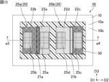
- FIG. 13 is a schematic plan view showing another example of a passive electronic component according to embodiment 1 of the present invention.
- FIG. 14 is a schematic cross-sectional view showing an example of a cross-section along line a3-a4 of the passive electronic component shown in FIG. 13.
- a step is provided on the surface of the second internal electrode layer 22b facing the substrate 10. Also, in the example shown in FIG. 14, a step is provided on the surface of the second internal electrode layer 22b facing away from the substrate 10.
- the second internal electrode layer 22b when the height in the first direction D1 is defined based on the first main surface 10a of the substrate 10, the second internal electrode layer 22b is bent so that the portion on one end side in the second direction D2 has a different height from the portion on the other end side in the second direction D2.
- a portion of the fourth internal electrode layer 22d overlaps the third internal electrode layer 22c in the first direction D1, sandwiching the second dielectric layer 23b.
- a step is provided on the surface of the fourth internal electrode layer 22d facing the substrate 10. Also, in the example shown in FIG. 14, a step is provided on the surface of the fourth internal electrode layer 22d facing away from the substrate 10.
- the fourth internal electrode layer 22d when the height in the first direction D1 is defined based on the first main surface 10a of the substrate 10, the fourth internal electrode layer 22d is bent so that the portion on one end side in the second direction D2 has a different height from the portion on the other end side in the second direction D2.
- the second external electrode 25b is connected to a portion of the second internal electrode layer 22b that does not overlap with the first internal electrode layer 22a in the first direction D1.
- the fourth external electrode 25d is connected to a portion of the fourth internal electrode layer 22d that does not overlap with the third internal electrode layer 22c in the first direction D1.
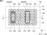
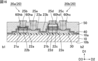
- FIG. 15 is a schematic plan view showing an example of a passive electronic component according to embodiment 2 of the present invention.
- FIG. 16 is a schematic cross-sectional view showing an example of a cross-section along line segment b1-b2 of the passive electronic component shown in FIG. 15.
- the second capacitance forming portion 21b further includes a first dielectric layer 23a and a fifth internal electrode layer 22e, which are stacked in order on the substrate 10 side in the first direction D1 with respect to the third internal electrode layer 22c.
- a capacitor element formed by the third internal electrode layer 22c, the second dielectric layer 23b, and the fourth internal electrode layer 22d is connected in series with a capacitor element formed by the third internal electrode layer 22c, the first dielectric layer 23a, and the fifth internal electrode layer 22e.
- a capacitor element including a first dielectric layer 23a and a capacitor element including a second dielectric layer 23b are connected in series, thereby realizing a capacitance equivalent to that of a capacitor element having a laminate of the first dielectric layer 23a and the second dielectric layer 23b as a dielectric layer.
- the configuration in which the two capacitor elements described above are connected in series reduces the electric field leaking from the end of the internal electrode layer (e.g., the end in the second direction D2). Therefore, in the second capacitance forming portion 21b of the passive electronic component 2A, not only is the parasitic capacitance between the internal electrode layers reduced, but the decrease in the Q value due to the parasitic capacitance is also suppressed.
- the configuration in which the two capacitor elements described above are connected in series reduces the capacitance deviation compared to a configuration consisting of only one capacitor element.
- the greater the number of capacitor elements connected in series the smaller the capacitance deviation tends to be.
- the two capacitor elements described above are connected in series in the first direction D1, so that the second capacitor 20b and therefore the passive electronic component 2A can be made smaller than when the two capacitor elements are connected in series in a direction perpendicular to the first direction D1, for example, in the second direction D2.
- the fifth internal electrode layer 22e may extend more in a direction perpendicular to the first direction D1 (e.g., the second direction D2 or the third direction D3) than the third internal electrode layer 22c and the fourth internal electrode layer 22d.
- the first capacitor 20a further has a first external electrode 25a connected to the first internal electrode layer 22a.
- the first capacitor 20a further has a second external electrode 25b connected to the second internal electrode layer 22b.
- second capacitor 20b further has a third external electrode 25c connected to the fifth internal electrode layer 22e.
- the third external electrode 25c is connected to a portion of the fifth internal electrode layer 22e that does not overlap with the third internal electrode layer 22c and the fourth internal electrode layer 22d in the first direction D1.
- the third external electrode 25c does not overlap the third internal electrode layer 22c and the fourth internal electrode layer 22d.
- the parasitic capacitance between the third external electrode 25c and the third internal electrode layer 22c and the parasitic capacitance between the third external electrode 25c and the fourth internal electrode layer 22d are minimized, which makes it easier to increase the Q value of the passive electronic component 2A.
- the second capacitor 20b further has a fourth external electrode 25d connected to the fourth internal electrode layer 22d.
- the periphery of the fourth external electrode 25d is located inside the periphery of the fourth internal electrode layer 22d.
- the parasitic capacitance between the fourth external electrode 25d and the third internal electrode layer 22c, and the parasitic capacitance between the fourth external electrode 25d and the fifth internal electrode layer 22e are minimized, which makes it easier to increase the Q value of the passive electronic component 2A.
- the passive electronic component 2A is manufactured in the same manner as the passive electronic component 1A, except that the fifth internal electrode layer 22e is also formed in the process of forming the first internal electrode layer 22a.
- the fifth internal electrode layer 22e is also formed in the process of forming the first internal electrode layer 22a.
- the first internal electrode layer 22a and the fifth internal electrode layer 22e are formed at the same time, but they may be formed at different times.
- the shape of the internal electrode layer may be different from the example shown in FIG. 15 and FIG. 16.
- the position of the external electrode may be different from the example shown in FIG. 15 and FIG. 16.
- FIG. 17 is a schematic plan view showing another example of a passive electronic component according to embodiment 2 of the present invention.
- FIG. 18 is a schematic cross-sectional view showing an example of a cross-section along line segment b3-b4 of the passive electronic component shown in FIG. 17.
- a step is provided on the surface of the second internal electrode layer 22b facing the substrate 10. Also, in the example shown in FIG. 18, a step is provided on the surface of the second internal electrode layer 22b facing away from the substrate 10.
- the second internal electrode layer 22b when the height in the first direction D1 is defined based on the first main surface 10a of the substrate 10, the second internal electrode layer 22b is bent so that the portion on one end side in the second direction D2 has a different height from the portion on the other end side in the second direction D2.
- a portion of the fourth internal electrode layer 22d overlaps the third internal electrode layer 22c in the first direction D1, sandwiching the second dielectric layer 23b.
- a step is provided on the surface of the fourth internal electrode layer 22d facing the substrate 10. Also, in the example shown in FIG. 18, a step is provided on the surface of the fourth internal electrode layer 22d facing away from the substrate 10.
- the fourth internal electrode layer 22d when the height in the first direction D1 is defined based on the first main surface 10a of the substrate 10, the fourth internal electrode layer 22d is bent so that the portion on one end side in the second direction D2 is at a different height than the portion on the other end side in the second direction D2.
- the fourth external electrode 25d is connected to a portion of the fourth internal electrode layer 22d that does not overlap with the third internal electrode layer 22c in the first direction D1.
- the passive electronic component of the third embodiment of the present invention differs from the passive electronic component of the second embodiment of the present invention in that it further includes an inductor formed by winding an internal wiring including at least one conductor layer.
- the direction of the winding axis of the internal wiring is perpendicular to the first main surface of the substrate, and all of the conductor layers each independently contain the same material as the first internal electrode layer, the second internal electrode layer, the third internal electrode layer, the fourth internal electrode layer, the fifth internal electrode layer, the first external electrode, the second external electrode, the third external electrode, or the fourth external electrode.
- FIG. 19 is an equivalent circuit diagram showing an example of a passive electronic component according to embodiment 3 of the present invention.
- FIG. 20 is a schematic plan view showing an example of a passive electronic component according to embodiment 3 of the present invention.
- FIG. 21 is a schematic cross-sectional view showing an example of a cross-section along line segment c1-c2 of the passive electronic component shown in FIG. 20.
- FIG. 22 is a schematic cross-sectional view showing an example of a cross-section along line segment d1-d2 of the passive electronic component shown in FIG. 20.
- FIG. 23 is a schematic cross-sectional view showing an example of a cross-section along line segment e1-e2 of the passive electronic component shown in FIG. 20.
- the passive electronic component 3A shown in Figures 19, 20, 21, 22, and 23 further includes an inductor 100 in addition to the substrate 10, the first capacitor 20a, and the second capacitor 20b.
- the first capacitor 20a and the second capacitor 20b are connected in series. Specifically, the first external electrode 25a of the first capacitor 20a and the fourth external electrode 25d of the second capacitor 20b are connected, so that the first capacitor 20a and the second capacitor 20b are connected in series.
- the first capacitor 20a is electrically connected to the outside of the passive electronic component 3A via the second external electrode 25b.
- the second capacitor 20b is electrically connected to the outside of the passive electronic component 3A via the third external electrode 25c.
- One end of the inductor 100 is connected to the connection between the first capacitor 20a and the second capacitor 20b. Specifically, one end of the inductor 100 is connected to the connection between the first external electrode 25a of the first capacitor 20a and the fourth external electrode 25d of the second capacitor 20b.
- the inductor 100 is connected to both the first capacitor 20a and the second capacitor 20b.
- the inductor 100 may be connected to one of the first capacitor 20a and the second capacitor 20b.
- the inductor 100 may be connected to at least one of the first capacitor 20a and the second capacitor 20b.
- the other end of the inductor 100 is connected to the fifth external electrode 25e.
- the inductor 100 is electrically led out to the outside of the passive electronic component 3A via the fifth external electrode 25e.
- the inductor 100 is made up of internal wiring 110 wound around it.
- the internal wiring 110 is wound in a spiral shape along the direction of the winding axis.
- the direction of the winding axis of the internal wiring 110 is perpendicular to the first main surface 10a of the substrate 10.
- the direction of the winding axis of the internal wiring 110 is parallel to the first direction D1.
- the internal wiring 110 is wound in a spiral shape when viewed from the first direction D1.
- the internal wiring 110 includes at least one conductor layer.
- the internal wiring 110 includes three conductor layers: a first conductor layer 111a, a second conductor layer 111b, and a third conductor layer 111c.
- the first conductor layer 111a and the laminate of the second conductor layer 111b and third conductor layer 111c are connected in sequence along the path of the internal wiring 110 that extends from one end side of the inductor 100 (the side of the first capacitor 20a and the second capacitor 20b) to the other end side of the inductor 100 (the side opposite the first capacitor 20a and the second capacitor 20b).
- All of the conductor layers included in the internal wiring 110 each independently contain the same material as the first internal electrode layer 22a, the second internal electrode layer 22b, the third internal electrode layer 22c, the fourth internal electrode layer 22d, the fifth internal electrode layer 22e, the first external electrode 25a, the second external electrode 25b, the third external electrode 25c, or the fourth external electrode 25d.
- the first conductor layer 111a contains the same material as the first external electrode 25a, the second external electrode 25b, the third external electrode 25c, or the fourth external electrode 25d.
- the second conductor layer 111b contains the same material as the second internal electrode layer 22b or the third internal electrode layer 22c.
- the third conductor layer 111c contains the same material as the first internal electrode layer 22a or the fifth internal electrode layer 22e.
- all the conductor layers included in the internal wiring 110 of the inductor 100 contain the same material as the internal electrode layers or external electrodes included in the first capacitor 20a and the second capacitor 20b, so that in the manufacturing process of the passive electronic component 3A, all the conductor layers can be formed at the same time as the internal electrode layers or external electrodes.
- the first conductor layer 111a can be formed at the same time as the first external electrode 25a, the second external electrode 25b, the third external electrode 25c, or the fourth external electrode 25d.
- the second conductor layer 111b can be formed at the same time as the second internal electrode layer 22b or the third internal electrode layer 22c.
- the third conductor layer 111c can be formed at the same time as the first internal electrode layer 22a or the fifth internal electrode layer 22e. Therefore, in the manufacturing process of the passive electronic component 3A, the inductor 100 can be formed at the same time as the first capacitor 20a and the second capacitor 20b.
- the inductor 100 can be formed at the same time as the first capacitor 20a and the second capacitor 20b, so the conductor layer included in the internal wiring 110 of the inductor 100 can be formed to be as thick as the internal electrode layer included in the first capacitor 20a and the second capacitor 20b. Therefore, in the passive electronic component 3A, it is possible to increase the Q value of the inductor 100.
- the passive electronic component 3A is manufactured in the same manner as the passive electronic component 2A, except that, for example, the third conductor layer 111c is formed in the process of forming the first internal electrode layer 22a or the fifth internal electrode layer 22e, the second conductor layer 111b is formed in the process of forming the second internal electrode layer 22b or the third internal electrode layer 22c, and the first conductor layer 111a is formed in the process of forming the first external electrode 25a, the second external electrode 25b, the third external electrode 25c, or the fourth external electrode 25d.
- the number of conductor layers included in the internal wiring of the inductor is not limited to the above-mentioned three layers, as long as it is at least one layer.
- the combination of materials for all conductor layers included in the internal wiring of the inductor is not limited to the above combinations, so long as it is a combination selected from the first internal electrode layer, the second internal electrode layer, the third internal electrode layer, the fourth internal electrode layer, the fifth internal electrode layer, the first external electrode, the second external electrode, the third external electrode, and the fourth external electrode.
- the passive electronic component of the fourth embodiment of the present invention differs from the passive electronic component of the second embodiment of the present invention in that it further includes an inductor formed by winding an internal wiring including a plurality of conductor layers.
- the direction of the winding axis of the internal wiring is parallel to the first main surface of the substrate, and all of the conductor layers each independently contain the same material as the first internal electrode layer, the second internal electrode layer, the third internal electrode layer, the fourth internal electrode layer, the fifth internal electrode layer, the first external electrode, the second external electrode, the third external electrode, or the fourth external electrode.
- the passive electronic component 4A shown in Figures 24, 25, and 26 further includes an inductor 200 in addition to the substrate 10, the first capacitor 20a, and the second capacitor 20b.
- the configuration of the first capacitor 20a and the second capacitor 20b in the passive electronic component 4A is similar to the configuration of the first capacitor 20a and the second capacitor 20b in the passive electronic component 3A.
- One end of the inductor 200 is connected to the connection between the first capacitor 20a and the second capacitor 20b. Specifically, one end of the inductor 200 is connected to the connection between the first external electrode 25a of the first capacitor 20a and the fourth external electrode 25d of the second capacitor 20b.
- the inductor 200 is connected to both the first capacitor 20a and the second capacitor 20b.
- the inductor 200 may be connected to one of the first capacitor 20a and the second capacitor 20b.
- the inductor 200 may be connected to at least one of the first capacitor 20a and the second capacitor 20b.
- the inductor 200 is electrically connected to the outside of the passive electronic component 4A at the other end.
- the inductor 200 is made up of internal wiring 210 wound around it.
- the internal wiring 210 is wound in a spiral shape along the direction of the winding axis.
- the direction of the winding axis of the internal wiring 210 is parallel to the first main surface 10a of the substrate 10.
- the direction of the winding axis of the internal wiring 210 is parallel to the second direction D2.
- the internal wiring 210 is wound in a spiral shape when viewed from the second direction D2.
- the internal wiring 210 includes multiple conductor layers.
- the internal wiring 210 includes nine conductor layers: a first conductor layer 211a, a second conductor layer 211b, a third conductor layer 211c, a fourth conductor layer 211d, a fifth conductor layer 211e, a sixth conductor layer 211f, a seventh conductor layer 211g, an eighth conductor layer 211h, and a ninth conductor layer 211j.
- All of the conductor layers included in the internal wiring 210 each independently contain the same material as the first internal electrode layer 22a, the second internal electrode layer 22b, the third internal electrode layer 22c, the fourth internal electrode layer 22d, the fifth internal electrode layer 22e, the first external electrode 25a, the second external electrode 25b, the third external electrode 25c, or the fourth external electrode 25d.
- the first conductor layer 211a contains the same material as the first external electrode 25a, the second external electrode 25b, the third external electrode 25c, or the fourth external electrode 25d.
- the second conductor layer 211b contains the same material as the fourth internal electrode layer 22d.
- the third conductor layer 211c contains the same material as the second internal electrode layer 22b or the third internal electrode layer 22c.
- the fourth conductor layer 211d contains the same material as the first internal electrode layer 22a or the fifth internal electrode layer 22e.
- the fifth conductor layer 211e contains the same material as the first external electrode 25a, the second external electrode 25b, the third external electrode 25c, or the fourth external electrode 25d.
- the sixth conductor layer 211f contains the same material as the fourth internal electrode layer 22d.
- the seventh conductor layer 211g contains the same material as the second internal electrode layer 22b or the third internal electrode layer 22c.
- the eighth conductor layer 211h contains the same material as the first internal electrode layer 22a or the fifth internal electrode layer 22e.
- the ninth conductor layer 211j contains the same material as the first external electrode 25a, the second external electrode 25b, the third external electrode 25c, or the fourth external electrode 25d.
- all the conductor layers included in the internal wiring 210 of the inductor 200 contain the same material as the internal electrode layers or external electrodes included in the first capacitor 20a and the second capacitor 20b, so that in the manufacturing process of the passive electronic component 4A, all the conductor layers can be formed at the same time as the internal electrode layers or external electrodes.
- the first conductor layer 211a can be formed at the same time as the first external electrode 25a, the second external electrode 25b, the third external electrode 25c, or the fourth external electrode 25d.
- the second conductor layer 211b can be formed at the same time as the fourth internal electrode layer 22d.
- the third conductor layer 211c can be formed at the same time as the second internal electrode layer 22b or the third internal electrode layer 22c.
- the fourth conductor layer 211d can be formed at the same time as the first internal electrode layer 22a or the fifth internal electrode layer 22e.
- the fifth conductor layer 211e can be formed at the same time as the first external electrode 25a, the second external electrode 25b, the third external electrode 25c, or the fourth external electrode 25d.
- the sixth conductor layer 211f can be formed at the same time as the fourth internal electrode layer 22d.
- the seventh conductor layer 211g can be formed at the same time as the second internal electrode layer 22b or the third internal electrode layer 22c.
- the eighth conductor layer 211h can be formed at the same time as the first internal electrode layer 22a or the fifth internal electrode layer 22e.
- the ninth conductor layer 211j can be formed at the same time as the first external electrode 25a, the second external electrode 25b, the third external electrode 25c, or the fourth external electrode 25d. Therefore, in the manufacturing process of the passive electronic component 4A, the inductor 200 can be formed at the same time as the first capacitor 20a and the second capacitor 20b.
- the inductor 200 can be formed at the same time as the first capacitor 20a and the second capacitor 20b, so the conductor layer included in the internal wiring 210 of the inductor 200 can be formed as thick as the internal electrode layer included in the first capacitor 20a and the second capacitor 20b. Therefore, in the passive electronic component 4A, it is possible to increase the Q value of the inductor 200.
- the direction of the winding axis of the internal wiring 210 of the inductor 200 is parallel to the first main surface 10a of the substrate 10, so the amount of magnetic flux penetrating the substrate 10 is reduced compared to the passive electronic component 3A in which the direction of the winding axis of the internal wiring 110 of the inductor 100 is perpendicular to the first main surface 10a of the substrate 10. Therefore, in the passive electronic component 4A, it is possible to increase the Q value of the inductor 200.
- the passive electronic component 4A is manufactured in the same manner as the passive electronic component 2A, except that, for example, the fourth conductor layer 211d and the eighth conductor layer 211h are formed in the process of forming the first internal electrode layer 22a or the fifth internal electrode layer 22e, the third conductor layer 211c and the seventh conductor layer 211g are formed in the process of forming the second internal electrode layer 22b or the third internal electrode layer 22c, the second conductor layer 211b and the sixth conductor layer 211f are formed in the process of forming the fourth internal electrode layer 22d, and the first conductor layer 211a, the fifth conductor layer 211e, and the ninth conductor layer 211j are formed in the process of forming the first external electrode 25a, the second external electrode 25b, the third external electrode 25c, or the fourth external electrode 25d.
- the number of conductor layers included in the internal wiring of the inductor is not limited to the above-mentioned nine layers, so long as there are multiple layers.
- the combination of materials for all conductor layers included in the internal wiring of the inductor is not limited to the above combinations, so long as it is a combination selected from the first internal electrode layer, the second internal electrode layer, the third internal electrode layer, the fourth internal electrode layer, the fifth internal electrode layer, the first external electrode, the second external electrode, the third external electrode, and the fourth external electrode.
- the case where the entire second internal electrode layer and the entire third internal electrode layer are in contact with the surface of the first dielectric layer opposite the substrate has been exemplified, but it is sufficient that at least a part of the second internal electrode layer and at least a part of the third internal electrode layer are in contact with the surface of the first dielectric layer opposite the substrate.
- what is in contact with the surface of the first dielectric layer opposite the substrate may be a combination of a part of the second internal electrode layer and a part of the third internal electrode layer, a combination of the entire second internal electrode layer and a part of the third internal electrode layer, a combination of a part of the second internal electrode layer and the entire third internal electrode layer, or a combination of the entire second internal electrode layer and the entire third internal electrode layer.
- each capacitor element constituting the capacitance forming portion does not include a laminate of multiple dielectric layers, but includes one dielectric layer.
- one capacitor element constituting the first capacitance forming portion 21a of the first capacitor 20a includes one first dielectric layer 23a.
- one capacitor element constituting the second capacitance forming portion 21b of the second capacitor 20b includes one second dielectric layer 23b.
- the passive electronic component of the present invention has a moisture-resistant protective layer
- the moisture-resistant protective layer covers the capacitance forming portions of all the capacitors (including the first capacitor and the second capacitor).
- the passive electronic component of the present invention has a resin protective layer, it is preferable that the resin protective layer covers the substrate and the capacitance forming portions of all the capacitors (including the first capacitor and the second capacitor).
- a substrate having a first main surface and a second main surface facing each other in a first direction; a plurality of capacitors provided on the first main surface side of the substrate; the plurality of capacitors include a first capacitor and a second capacitor spaced apart from the first capacitor in a second direction perpendicular to the first direction;
- the first capacitor has a first capacitance forming portion including a first internal electrode layer, a first dielectric layer, and a second internal electrode layer, which are laminated in this order from the substrate side in the first direction;
- the second capacitor has a second capacitance forming portion including a third internal electrode layer, a second dielectric layer, and a fourth internal electrode layer, which are laminated in this order from the substrate side in the first direction,
- a passive electronic component characterized in that at least a portion of the second internal electrode layer and at least a portion of the third internal electrode layer are in contact with a surface of the first dielectric layer opposite the substrate.
- the first capacitor further comprises a first external electrode connected to the first internal electrode layer and a second external electrode connected to the second internal electrode layer;
- the first capacitor further comprises a first external electrode connected to the first internal electrode layer and a second external electrode connected to the second internal electrode layer;
- the passive electronic component described in ⁇ 4>, wherein the second capacitor further has a third external electrode connected to the fifth internal electrode layer and a fourth external electrode connected to the fourth internal electrode layer.
- ⁇ 6> The passive electronic component according to ⁇ 3> or ⁇ 5>, wherein, when viewed in a plan view from the first direction, a periphery of the second external electrode is located inside a periphery of the second internal electrode layer.
- ⁇ 7> The passive electronic component according to ⁇ 3> or ⁇ 5>, wherein, when viewed in a plan view from the first direction, a periphery of the fourth external electrode is located inside a periphery of the fourth internal electrode layer.
- the inductor further includes an internal wiring including at least one conductor layer wound around the inductor. a direction of a winding axis of the internal wiring is perpendicular to the first main surface of the substrate,
- the inductor further includes an internal wiring including a plurality of conductor layers wound around the inductor. a direction of a winding axis of the internal wiring is parallel to the first main surface of the substrate,
- the passive electronic component according to any one of ⁇ 1> to ⁇ 9>, further comprising an insulating layer provided between the substrate and the first capacitor in the first direction, and between the substrate and the second capacitor in the first direction.
Landscapes
- Engineering & Computer Science (AREA)
- Power Engineering (AREA)
- Microelectronics & Electronic Packaging (AREA)
- Manufacturing & Machinery (AREA)
- Fixed Capacitors And Capacitor Manufacturing Machines (AREA)
- Ceramic Capacitors (AREA)
Priority Applications (2)
| Application Number | Priority Date | Filing Date | Title |
|---|---|---|---|
| JP2025544237A JPWO2025052920A1 (https=) | 2023-09-08 | 2024-08-21 | |
| CN202480052133.5A CN121693790A (zh) | 2023-09-08 | 2024-08-21 | 无源电子部件 |
Applications Claiming Priority (2)
| Application Number | Priority Date | Filing Date | Title |
|---|---|---|---|
| JP2023-146226 | 2023-09-08 | ||
| JP2023146226 | 2023-09-08 |
Publications (1)
| Publication Number | Publication Date |
|---|---|
| WO2025052920A1 true WO2025052920A1 (ja) | 2025-03-13 |
Family
ID=94923507
Family Applications (1)
| Application Number | Title | Priority Date | Filing Date |
|---|---|---|---|
| PCT/JP2024/029567 Pending WO2025052920A1 (ja) | 2023-09-08 | 2024-08-21 | 受動電子部品 |
Country Status (3)
| Country | Link |
|---|---|
| JP (1) | JPWO2025052920A1 (https=) |
| CN (1) | CN121693790A (https=) |
| WO (1) | WO2025052920A1 (https=) |
Cited By (1)
| Publication number | Priority date | Publication date | Assignee | Title |
|---|---|---|---|---|
| WO2025263314A1 (ja) * | 2024-06-17 | 2025-12-26 | 株式会社村田製作所 | 受動電子部品及び受動電子部品の製造方法 |
Citations (3)
| Publication number | Priority date | Publication date | Assignee | Title |
|---|---|---|---|---|
| JPH09121023A (ja) * | 1995-10-25 | 1997-05-06 | Olympus Optical Co Ltd | 半導体装置 |
| JP2022103601A (ja) * | 2020-12-28 | 2022-07-08 | Tdk株式会社 | 電子部品及びその製造方法 |
| WO2022239717A1 (ja) * | 2021-05-10 | 2022-11-17 | 株式会社村田製作所 | 半導体装置 |
-
2024
- 2024-08-21 CN CN202480052133.5A patent/CN121693790A/zh active Pending
- 2024-08-21 JP JP2025544237A patent/JPWO2025052920A1/ja active Pending
- 2024-08-21 WO PCT/JP2024/029567 patent/WO2025052920A1/ja active Pending
Patent Citations (3)
| Publication number | Priority date | Publication date | Assignee | Title |
|---|---|---|---|---|
| JPH09121023A (ja) * | 1995-10-25 | 1997-05-06 | Olympus Optical Co Ltd | 半導体装置 |
| JP2022103601A (ja) * | 2020-12-28 | 2022-07-08 | Tdk株式会社 | 電子部品及びその製造方法 |
| WO2022239717A1 (ja) * | 2021-05-10 | 2022-11-17 | 株式会社村田製作所 | 半導体装置 |
Cited By (1)
| Publication number | Priority date | Publication date | Assignee | Title |
|---|---|---|---|---|
| WO2025263314A1 (ja) * | 2024-06-17 | 2025-12-26 | 株式会社村田製作所 | 受動電子部品及び受動電子部品の製造方法 |
Also Published As
| Publication number | Publication date |
|---|---|
| CN121693790A (zh) | 2026-03-17 |
| JPWO2025052920A1 (https=) | 2025-03-13 |
Similar Documents
| Publication | Publication Date | Title |
|---|---|---|
| US8050045B2 (en) | Electronic component and method of manufacturing the same | |
| JP7323343B2 (ja) | チップ部品 | |
| JP4450071B2 (ja) | 電子部品 | |
| CN100538926C (zh) | 薄膜共模滤波器和薄膜共模滤波器阵列 | |
| JP6856095B2 (ja) | キャパシタ | |
| US8766103B2 (en) | Electronic component | |
| WO2025052920A1 (ja) | 受動電子部品 | |
| JP7505629B2 (ja) | キャパシタ | |
| US20130271251A1 (en) | Substrate-Less Electronic Component | |
| WO2019235510A1 (ja) | コイル部品及びその製造方法 | |
| JP2021048419A (ja) | 積層型インダクタ部品 | |
| JP7677224B2 (ja) | コイル部品 | |
| TWI817244B (zh) | 被動零件 | |
| JP6968680B2 (ja) | 積層型インダクタ部品 | |
| CN110098054B (zh) | 电容器组件 | |
| JP7283434B2 (ja) | 集積受動部品 | |
| US20210027951A1 (en) | Capacitor cluster | |
| JP7758199B2 (ja) | 電子部品 | |
| US20240266283A1 (en) | Multilayer-type on-chip inductor structure | |
| JP7776023B2 (ja) | 集積化受動部品 | |
| WO2025052919A1 (ja) | 受動電子部品 | |
| WO2023181806A1 (ja) | 電子部品 | |
| WO2023181917A1 (ja) | 電子部品の製造方法 | |
| WO2025263314A1 (ja) | 受動電子部品及び受動電子部品の製造方法 | |
| WO2022085715A1 (ja) | 多層構造体およびその製造方法 |
Legal Events
| Date | Code | Title | Description |
|---|---|---|---|
| 121 | Ep: the epo has been informed by wipo that ep was designated in this application |
Ref document number: 24862574 Country of ref document: EP Kind code of ref document: A1 |
|
| ENP | Entry into the national phase |
Ref document number: 2025544237 Country of ref document: JP Kind code of ref document: A |
|
| WWE | Wipo information: entry into national phase |
Ref document number: 2025544237 Country of ref document: JP |