WO2025041831A1 - 導電性粒子、導電性粒子の製造方法、導電材料及び接続構造体 - Google Patents
導電性粒子、導電性粒子の製造方法、導電材料及び接続構造体 Download PDFInfo
- Publication number
- WO2025041831A1 WO2025041831A1 PCT/JP2024/029840 JP2024029840W WO2025041831A1 WO 2025041831 A1 WO2025041831 A1 WO 2025041831A1 JP 2024029840 W JP2024029840 W JP 2024029840W WO 2025041831 A1 WO2025041831 A1 WO 2025041831A1
- Authority
- WO
- WIPO (PCT)
- Prior art keywords
- conductive
- particles
- less
- particle
- weight
- Prior art date
- Legal status (The legal status is an assumption and is not a legal conclusion. Google has not performed a legal analysis and makes no representation as to the accuracy of the status listed.)
- Pending
Links
Images




Classifications
-
- H—ELECTRICITY
- H01—ELECTRIC ELEMENTS
- H01B—CABLES; CONDUCTORS; INSULATORS; SELECTION OF MATERIALS FOR THEIR CONDUCTIVE, INSULATING OR DIELECTRIC PROPERTIES
- H01B1/00—Conductors or conductive bodies characterised by the conductive materials; Selection of materials as conductors
-
- H—ELECTRICITY
- H01—ELECTRIC ELEMENTS
- H01B—CABLES; CONDUCTORS; INSULATORS; SELECTION OF MATERIALS FOR THEIR CONDUCTIVE, INSULATING OR DIELECTRIC PROPERTIES
- H01B1/00—Conductors or conductive bodies characterised by the conductive materials; Selection of materials as conductors
- H01B1/20—Conductive material dispersed in non-conductive organic material
- H01B1/22—Conductive material dispersed in non-conductive organic material the conductive material comprising metals or alloys
-
- H—ELECTRICITY
- H01—ELECTRIC ELEMENTS
- H01B—CABLES; CONDUCTORS; INSULATORS; SELECTION OF MATERIALS FOR THEIR CONDUCTIVE, INSULATING OR DIELECTRIC PROPERTIES
- H01B13/00—Apparatus or processes specially adapted for manufacturing conductors or cables
-
- H—ELECTRICITY
- H01—ELECTRIC ELEMENTS
- H01B—CABLES; CONDUCTORS; INSULATORS; SELECTION OF MATERIALS FOR THEIR CONDUCTIVE, INSULATING OR DIELECTRIC PROPERTIES
- H01B5/00—Non-insulated conductors or conductive bodies characterised by their form
-
- H—ELECTRICITY
- H01—ELECTRIC ELEMENTS
- H01B—CABLES; CONDUCTORS; INSULATORS; SELECTION OF MATERIALS FOR THEIR CONDUCTIVE, INSULATING OR DIELECTRIC PROPERTIES
- H01B5/00—Non-insulated conductors or conductive bodies characterised by their form
- H01B5/16—Non-insulated conductors or conductive bodies characterised by their form comprising conductive material in insulating or poorly conductive material, e.g. conductive rubber
-
- H—ELECTRICITY
- H01—ELECTRIC ELEMENTS
- H01R—ELECTRICALLY-CONDUCTIVE CONNECTIONS; STRUCTURAL ASSOCIATIONS OF A PLURALITY OF MUTUALLY-INSULATED ELECTRICAL CONNECTING ELEMENTS; COUPLING DEVICES; CURRENT COLLECTORS
- H01R11/00—Individual connecting elements providing two or more spaced connecting locations for conductive members which are, or may be, thereby interconnected, e.g. end pieces for wires or cables supported by the wire or cable and having means for facilitating electrical connection to some other wire, terminal, or conductive member, blocks of binding posts
- H01R11/01—Individual connecting elements providing two or more spaced connecting locations for conductive members which are, or may be, thereby interconnected, e.g. end pieces for wires or cables supported by the wire or cable and having means for facilitating electrical connection to some other wire, terminal, or conductive member, blocks of binding posts characterised by the form or arrangement of the conductive interconnection between the connecting locations
-
- H—ELECTRICITY
- H10—SEMICONDUCTOR DEVICES; ELECTRIC SOLID-STATE DEVICES NOT OTHERWISE PROVIDED FOR
- H10W—GENERIC PACKAGES, INTERCONNECTIONS, CONNECTORS OR OTHER CONSTRUCTIONAL DETAILS OF DEVICES COVERED BY CLASS H10
- H10W72/00—Interconnections or connectors in packages
- H10W72/071—Connecting or disconnecting
Definitions
- the present invention relates to a conductive particle having a base particle and a conductive portion disposed on the surface of the base particle, and a method for producing the same.
- the present invention also relates to a conductive material and a connection structure using the conductive particle.
- Anisotropic conductive materials such as anisotropic conductive pastes and anisotropic conductive films are widely known.
- anisotropic conductive materials conductive particles are dispersed in a binder resin.
- the anisotropic conductive material is used to obtain various connection structures.
- connections using the anisotropic conductive material include connections between a flexible printed circuit board and a glass substrate (FOG (Film on Glass)), connections between a semiconductor chip and a flexible printed circuit board (COF (Chip on Film)), connections between a semiconductor chip and a glass substrate (COG (Chip on Glass)), and connections between a flexible printed circuit board and a glass epoxy substrate (FOB (Film on Board)).
- connection In recent years, in order to reduce the burden on substrates, etc., mounting (conductive connection) is sometimes performed in a low-temperature environment (for example, 150°C or less). In order to improve the conductive connectivity when making a conductive connection at low temperatures, a method is sometimes used in which the metal on the surface of the conductive particles is melted and joined to the electrodes. In this case, when conventional conductive particles are used to electrically connect electrodes at a relatively low temperature to create a connection structure, there is an issue that melting of the metal in the conductive particles is difficult to occur, and the conductive reliability cannot be sufficiently increased (the connection resistance cannot be sufficiently reduced).
- Patent Document 1 discloses conductive microparticles in which an inner metal layer with a melting point of 900°C or higher is formed on the surface of a base microparticle, and an outer metal layer with a melting point of 350°C or lower is formed on the outside of the inner metal layer.
- conductive particles such as those described in Patent Document 1
- multiple conductive particles may aggregate during storage. If the conductive particles aggregate, there is a problem in that the connection resistance cannot be sufficiently reduced. With conventional conductive particles, it is difficult to improve both the performance of suppressing the aggregation of conductive particles and improving the conductive reliability of the connection structure obtained by conductive connection at relatively low temperatures.
- the object of the present invention is to provide conductive particles and a manufacturing method thereof that can suppress the aggregation of conductive particles and improve the electrical conductivity reliability of the resulting connection structure even when the conductive connection is made at a relatively low temperature. It is also an object of the present invention to provide a conductive material and a connection structure that use the conductive particles.
- This specification discloses the following conductive particles, a method for manufacturing conductive particles, a conductive material, and a connection structure.
- a conductive particle having a base particle and a conductive portion disposed on the surface of the base particle, the conductive portion containing tin and indium, and when the X-ray diffraction spectrum of the conductive portion is measured, peaks are present in a region of 20.5° to 23.5° and a region of 32.5° to 34°, and the ratio P of the area of the peak present in the region of 20.5° to 23.5° to the area of the peak present in the region of 32.5° to 34° is 0.0001 or more and 0.2 or less.
- Item 2 Conductive particles according to item 1, in which the total content of tin and indium is 5% by weight or more in 100% by weight of the conductive particles.
- Item 3 The conductive particles according to item 1 or 2, wherein the ratio P is 0.001 or more and 0.2 or less.
- Item 4 The conductive particles according to item 3, wherein the ratio P is 0.01 or more and 0.2 or less.
- Item 5 The conductive particles according to item 3, wherein the ratio P is 0.005 or more and 0.01 or less.
- Item 6 The conductive particles according to any one of items 1 to 5, wherein the particle diameter of the conductive particles is 1 ⁇ m or more and 100 ⁇ m or less.
- Item 7 A conductive particle according to any one of items 1 to 6, having a plurality of protrusions on the outer surface of the conductive portion.
- Item 8 A conductive particle according to any one of items 1 to 7, wherein the conductive part contains a metal salt, and the average content of the metal salt in a region that is 1/2 the thickness from the outer surface of the conductive part toward the inside exceeds 50% by weight, out of a total content of the metal salt in the conductive part of 100% by weight.
- Item 9 A conductive particle according to any one of items 1 to 8, wherein the conductive portion contains a metal salt, and the metal salt contains indium hydroxide.
- Item 10 A method for producing conductive particles according to any one of items 1 to 9, comprising forming the conductive portion on the surface of the base particle by electroless plating.
- Item 11 A conductive material comprising the conductive particles described in any one of items 1 to 9 and a binder resin.
- a connection structure comprising a first connection target member having a first electrode on its surface, a second connection target member having a second electrode on its surface, and a connection part connecting the first connection target member and the second connection target member, the material of the connection part containing the conductive particles described in any one of items 1 to 9, and the first electrode and the second electrode being electrically connected by the conductive particles.
- the conductive particle according to the present invention is a conductive particle having a base particle and a conductive portion disposed on the surface of the base particle.
- the conductive portion contains tin and indium.
- peaks are present in the region of 20.5° to 23.5° and in the region of 32.5° to 34°.
- the ratio P of the area of the peak present in the region of 20.5° to 23.5° to the area of the peak present in the region of 32.5° to 34° is 0.0001 or more and 0.2 or less. Since the conductive particle according to the present invention has the above configuration, it is possible to suppress the aggregation of the conductive particles and to increase the conductive reliability of the resulting connection structure even when the conductive connection is performed at a relatively low temperature.
- FIG. 1 is a cross-sectional view showing a conductive particle according to a first embodiment of the present invention.
- FIG. 2 is a cross-sectional view showing a conductive particle according to a second embodiment of the present invention.
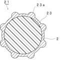
- FIG. 3 is a cross-sectional view showing a conductive particle according to a third embodiment of the present invention.
- FIG. 4 is a cross-sectional view showing a conductive particle according to a fourth embodiment of the present invention.
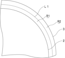
- FIG. 5 is a schematic diagram for explaining a region where the thickness is 1/2 from the outer surface toward the inside of the conductive portion.
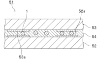
- FIG. 6 is a cross-sectional view that illustrates a connection structure using conductive particles according to the first embodiment of the present invention.
- FIG. 7 is an X-ray diffraction spectrum of the conductive portion of the conductive particle obtained in Example 7.
- the conductive particle according to the present invention is a conductive particle having a base particle and a conductive portion disposed on the surface of the base particle.
- the conductive portion contains tin and indium.
- peaks are present in the region of 20.5° to 23.5° and the region of 32.5° to 34°.
- the ratio P of the area of the peak present in the region of 20.5° to 23.5° to the area of the peak present in the region of 32.5° to 34° is 0.0001 to 0.2.
- the conductive particles according to the present invention have the above-mentioned configuration, so even if a conductive connection is made at a relatively low temperature (even when electrodes are electrically connected), the conductive part melts, thereby improving the reliability of conduction. In other words, the reliability of conduction between upper and lower electrodes that should be connected can be improved. In addition, because the conductive part melts quickly, the reliability of insulation between lateral electrodes that should not be connected can also be ensured.
- the surface is very soft, so multiple conductive particles may aggregate during storage. If the conductive particles aggregate, there is a problem that the connection resistance cannot be sufficiently reduced.
- the conductive particles according to the present invention have the above-mentioned configuration, and therefore it is possible to suppress the aggregation of the conductive particles.
- solder particles in which both the center portion and the outer surface portion of the conductive portion are formed from solder
- the entire particle is likely to melt and be crushed, so if there is variation in the distance between the upper and lower electrodes, sufficient joining cannot be achieved, and the reliability of the conductivity between the upper and lower electrodes that should be connected cannot be improved.
- crushed solder particles may protrude from between the electrodes, causing a short circuit between horizontal electrodes that should not be connected.
- conductive materials containing solder particles multiple solder particles tend to aggregate during storage and settle in the conductive material, so there is the issue that the connection resistance cannot be sufficiently low.
- the conductive particles according to the present invention have the above-mentioned configuration, and therefore, compared to solder particles in which both the center portion and the outer surface portion of the conductive portion are formed of solder, it is possible to improve the reliability of conductivity between upper and lower electrodes that should be connected, and to improve the reliability of insulation between lateral electrodes that should not be connected.
- the conductive particles according to the present invention have the above-mentioned configuration, it is possible to suppress agglomeration of the conductive particles.
- FIG. 1 is a cross-sectional view showing a conductive particle according to a first embodiment of the present invention.
- the conductive particle 1 shown in FIG. 1 has a base particle 2 and a conductive portion 3 disposed on the surface of the base particle 2.
- the conductive portion 3 covers the surface of the base particle 2.
- the conductive particle 1 is a coated particle in which the surface of the base particle 2 is coated with the conductive portion 3.
- the conductive portion 3 is a single-layer conductive layer.
- the conductive portion may be a single-layer conductive layer, or a multi-layer conductive layer composed of two or more layers.
- the conductive portion may cover the entire surface of the base particle, or may cover only a portion of it.
- the conductive portion 3 contains tin and indium.
- the ratio P of the area of the peak present in the region of 20.5° to 23.5° and the area of the peak present in the region of 32.5° to 34° and inclusive is 0.0001 or more and 0.2 or less.
- the conductive portion 3 is an alloy layer containing an alloy of two or more metals.
- the conductive portion may be an alloy layer containing an alloy of two types of metals, an alloy layer containing an alloy of three types of metals, or an alloy layer containing an alloy of three or more metals.
- the conductive portion may be an alloy layer containing an alloy of 10 or less metals, or an alloy layer containing an alloy of five or less metals.
- FIG. 2 is a cross-sectional view showing a conductive particle according to a second embodiment of the present invention.
- the conductive particle 11 shown in FIG. 2 has a base particle 2 and a conductive portion 13 disposed on the surface of the base particle 2.
- the conductive portion 13 coats the surface of the base particle 2.
- the conductive particle 11 is a coated particle in which the surface of the base particle 2 is coated with the conductive portion 13.
- the conductive portion 13 is a conductive layer having a two-layer structure.
- the conductive portion 13 has a first conductive portion 13A and a second conductive portion 13B.
- the first conductive portion 13A is disposed on the surface of the base particle 2.
- the first conductive portion 13A is in contact with the base particle 2.
- the first conductive portion 13A is disposed between the base particle 2 and the second conductive portion 13B.
- the second conductive portion 13B is disposed on the surface of the first conductive portion 13A.
- the second conductive portion 13B is in contact with the first conductive portion 13A.
- the second conductive portion 13B is the outermost conductive portion in the conductive particle 11.
- the conductive portion 13 may contain tin and indium.
- the first conductive portion 13A may contain tin, and the second conductive portion 13B may contain tin.
- the first conductive portion 13A may contain indium
- the second conductive portion 13B may contain indium.
- the first conductive portion 13A may contain tin and indium
- the second conductive portion 13B may contain tin and indium.
- the ratio P of the area of the peak present in the region of 20.5° to 23.5° inclusive to the area of the peak present in the region of 32.5° to 34° inclusive is 0.0001 or more and 0.2 or less.
- the conductive portion may have an alloy layer containing an alloy of two or more metals.
- the first conductive portion may be an alloy layer containing an alloy of two or more metals
- the second conductive portion may be an alloy layer containing an alloy of two or more metals.
- the first conductive portion may be an alloy layer containing an alloy of 10 or less metals, or an alloy layer containing an alloy of 5 or less metals.
- the second conductive portion may be an alloy layer containing an alloy of 10 or less metals, or an alloy layer containing an alloy of 5 or less metals.
- FIG. 3 is a cross-sectional view showing a conductive particle according to a third embodiment of the present invention.
- the conductive particle 21 shown in FIG. 3 has a base particle 2 and a conductive portion 23 disposed on the surface of the base particle 2.
- the conductive portion 23 covers the surface of the base particle 2.
- the conductive particle 21 is a coated particle in which the surface of the base particle 2 is coated with the conductive portion 23.
- the conductive portion 23 is a single conductive layer.
- the conductive particle 21 (particularly, the conductive portion 23) has a plurality of protrusions 23a on its surface.
- the core material is not disposed on the surface of the base particle 2.
- the conductive particle 21 does not have a core material.
- the conductive portion 23 contains tin and indium.
- peaks are present in the region of 20.5° to 23.5° and inclusive and in the region of 32.5° to 34° inclusive.
- the ratio P of the area of the peak present in the region of 20.5° to 23.5° inclusive to the area of the peak present in the region of 32.5° to 34° inclusive is 0.0001 or more and 0.2 or less.
- FIG. 4 is a cross-sectional view showing a conductive particle according to a fourth embodiment of the present invention.
- the conductive particle 31 shown in FIG. 4 has a base particle 2, a conductive portion 33 arranged on the surface of the base particle 2, and a plurality of core materials 34.
- the conductive portion 33 is a single conductive layer.
- the conductive particle 31 (particularly, the conductive portion 33) has a plurality of protrusions 33a on its surface.
- a plurality of core substances 34 are disposed on the surface of the base particle 2.
- the plurality of core substances 34 are embedded within the conductive portion 33.
- the core substances 34 are disposed inside the protrusions 33a.
- the conductive portion 33 covers the plurality of core substances 34.
- the outer surface of the conductive portion 33 is raised by the plurality of core substances 34, forming the protrusions 33a.
- the conductive portion 33 contains tin and indium.
- the ratio P of the area of the peak present in the region of 20.5° to 23.5° and the area of the peak present in the region of 32.5° to 34° and inclusive is 0.0001 or more and 0.2 or less.
- (meth)acrylate refers to acrylate and methacrylate.
- (meth)acrylic refers to acrylic and methacrylic.
- (meth)acryloyl refers to acryloyl and methacryloyl.
- the highest peak height in the region of 32.5° to 34° is higher than the highest peak height in the region of 20.5° to 23.5°.
- the volume resistivity of the conductive particles can be reduced, and as a result, the initial conductive reliability of the resulting connection structure can be improved.
- the X-ray diffraction spectrum of the conductive part of the conductive particle is measured, at least one peak is present in the region of 20.5° to 23.5°.
- the X-ray diffraction spectrum of the conductive part of the conductive particle is measured, at least one peak is present in the region of 32.5° to 34°.
- one peak or multiple peaks may be present in the region of 20.5° to 23.5°.
- one peak or multiple peaks may be present in the region of 32.5° to 34°.
- a peak may be present in a region other than the region of 20.5° to 23.5° and the region of 32.5° to 34°.
- "there is a peak" in a certain region means that the entire peak (from the start point to the end point) is present in that region.
- the X-ray diffraction spectrum of the conductive part can be measured using an X-ray diffraction device (e.g., Rigaku Denki's "RINT2500VHF").
- the X-ray diffraction spectrum of the conductive part can be measured, for example, under conditions of 45 kV, 50 mA, a scan rate of 4.0 deg/min, a scan step of 0.02 deg, and a measurement range of 2 ⁇ from 5.0 deg to 60.0 deg.
- the X-ray diffraction spectrum of the conductive part is preferably measured at intervals of 0.10° or less, more preferably at intervals of 0.05° or less, even more preferably at intervals of 0.02° or less, and particularly preferably at intervals of less than 0.02°.
- the X-ray diffraction spectrum of the conductive part is preferably measured in a range that includes the entire range from 20.5° to 34°.
- the ratio P of the area of the peak present in the region of 20.5° to 23.5° to the area of the peak present in the region of 32.5° to 34° is 0.0001 or more and 0.2 or less.
- the ratio of the area of the peak present in the region of 20.5° to 23.5° to the area of the peak present in the region of 32.5° to 34° is defined as the ratio P (area of the peak present in the region of 20.5° to 23.5°/area of the peak present in the region of 32.5° to 34°).
- the ratio P is 0.0001 or more and 0.2 or less.
- the ratio P is preferably 0.0005 or more, more preferably 0.0007 or more, even more preferably 0.001 or more, even more preferably 0.003 or more, particularly preferably 0.005 or more, and preferably 0.15 or less, more preferably 0.10 or less, and even more preferably 0.05 or less.
- the ratio P is equal to or more than the lower limit, the aggregation of the conductive particles can be more effectively suppressed.
- the ratio P is equal to or less than the upper limit, the volume resistivity of the conductive particles can be further reduced, and the conductive reliability of the resulting connection structure can be further improved even when the conductive connection is performed at a relatively low temperature.
- the ratio P is preferably 0.01 or more, and more preferably 0.01 to 0.2. From the viewpoint of further reducing the volume resistivity of the conductive particles and further increasing the electrical reliability of the resulting connection structure even when the conductive connection is performed at a relatively low temperature, the ratio P is preferably 0.01 or less, and more preferably 0.001 to 0.01. From the viewpoint of more effectively suppressing the aggregation of the conductive particles, further reducing the volume resistivity of the conductive particles, and further increasing the electrical reliability of the resulting connection structure even when the conductive connection is performed at a relatively low temperature, the ratio P is preferably 0.005 to 0.01. The range of the ratio P can be set by appropriately selecting the lower limit value and the upper limit value.
- the area of the peaks in each region in the X-ray diffraction spectrum of the conductive part can be measured, for example, as follows.
- the average value of the regions in which no peaks exist is calculated from the obtained spectrum, and this is taken as the baseline count value.
- the sum of the values obtained by subtracting the baseline count value from each count value of the peaks in the region of 20.5° to 23.5° is taken as the "area of the peaks in the region of 20.5° to 23.5°”.
- the sum of the values obtained by subtracting the baseline count value (background noise) from the count values of the peaks in the region of 32.5° to 34° is taken as the "area of the peaks in the region of 32.5° to 34°".
- Methods for easily controlling the ratio P within a preferred range include, for example, the following methods.
- methods for increasing the value of the ratio P include, for example, the following methods.
- a method of increasing the amount of metal salt in the plating solution in electroless plating when forming the conductive part A method of increasing the amount of strong acid or strong base added to precipitate a metal salt in the above-mentioned electroless plating (increasing the concentration or dripping speed, or lengthening the dripping time).
- the ratio P can be controlled by the content of metal salt in the conductive portion. Specifically, the value of the ratio P increases by increasing the content of metal salt in the conductive portion relative to the metal contained in the conductive portion as a simple metal or an alloy. The value of the ratio P decreases by decreasing the content of metal salt in the conductive portion relative to the metal contained in the conductive portion as a simple metal or an alloy.
- the area of the peaks in the region of 20.5° to 23.5° and the area of the peaks in the region of 32.5° to 34° indicate the total area of all peaks in the region.
- the particle diameter of the conductive particles is preferably 1 ⁇ m or more, more preferably 3 ⁇ m or more, and even more preferably 5 ⁇ m or more, and is preferably 100 ⁇ m or less, more preferably 50 ⁇ m or less, and even more preferably 40 ⁇ m or less.
- the particle diameter of the conductive particles is equal to or more than the above lower limit and equal to or less than the above upper limit, the conductivity reliability and insulation reliability can be improved.
- the particle diameter of the conductive particles is preferably an average particle diameter, and the average particle diameter indicates a number average particle diameter.
- the particle diameter of the conductive particles can be determined, for example, by observing 50 random conductive particles with an electron microscope or optical microscope and calculating the average particle diameter of each conductive particle, or by performing laser diffraction particle size distribution measurement.
- the coefficient of variation (CV value) of the particle diameter of the conductive particles is preferably 10% or less, and more preferably 5% or less. There is no particular lower limit to the coefficient of variation (CV value) of the particle diameter of the conductive particles.
- the coefficient of variation (CV value) of the particle diameter of the conductive particles may be 0% or more, or 1% or more.
- CV value The above coefficient of variation (CV value) can be measured as follows.
- CV value (%) ( ⁇ /Dn) ⁇ 100 ⁇ : Standard deviation of the particle diameter of the conductive particles Dn: Average particle diameter of the conductive particles
- the shape of the conductive particles is not particularly limited.
- the conductive particles may be spherical, may be non-spherical, or may be flat, etc.
- the 10% K value of the conductive particles is preferably 500 N/ mm2 or more, more preferably 1000 N/ mm2 or more, and preferably 17000 N/mm2 or less , more preferably 13000 N/ mm2 or less.
- the 10% K value of the conductive particles can be measured, for example, as follows.
- the conductive particles are compressed with the smooth end face of a cylindrical indenter (diameter 50 ⁇ m, made of diamond) at 25°C under conditions where a maximum test load of 60 mN is applied for 20 seconds.
- the load value (N) and compression displacement (mm) at this time are measured.
- the 10% K value compressive elastic modulus
- the micro-compression testing machine for example, the Fischer Scope H-100 manufactured by Fischer can be used.
- the conductive particles are dispersed in a binder resin and are suitable for use in obtaining a conductive material.
- the base particles include resin particles, inorganic particles other than metal particles, organic-inorganic hybrid particles, and metal particles.
- the base particles are preferably base particles other than metal particles, and more preferably resin particles, inorganic particles other than metal particles, or organic-inorganic hybrid particles.
- the base particles may be core-shell particles having a core and a shell disposed on the surface of the core.
- the core may be an organic core, and the shell may be an inorganic shell.
- the materials of the resin particles include polyolefin resins such as polyethylene, polypropylene, polystyrene, polyvinyl chloride, polyvinylidene chloride, polyisobutylene, and polybutadiene; acrylic resins such as polymethyl methacrylate and polymethyl acrylate; polycarbonate, polyamide, phenol formaldehyde resin, melamine formaldehyde resin, benzoguanamine formaldehyde resin, urea formaldehyde resin, phenol resin, melamine resin, benzoguanamine resin, urea resin, epoxy resin, unsaturated polyester resin, saturated polyester resin, polyethylene terephthalate, polysulfone, polyphenylene oxide, polyacetal, polyimide, polyamideimide, polyether ether ketone, polyether sulfone, and divinylbenzene polymer.
- polyolefin resins such as polyethylene, polypropylene, polystyrene, polyvinyl chloride, poly
- the divinylbenzene polymer may be a divinylbenzene copolymer.
- examples of the divinylbenzene copolymer include divinylbenzene-styrene copolymer and divinylbenzene-(meth)acrylic acid ester copolymer. Since the hardness of the resin particles can be easily controlled within a suitable range, it is preferable that the material of the resin particles is a polymer obtained by polymerizing one or more polymerizable monomers having an ethylenically unsaturated group.
- the polymerizable monomer having an ethylenically unsaturated group may be a non-crosslinkable monomer or a crosslinkable monomer.
- the non-crosslinkable monomers include styrene-based monomers such as styrene and ⁇ -methylstyrene; carboxyl group-containing monomers such as (meth)acrylic acid, maleic acid, and maleic anhydride; alkyl (meth)acrylate compounds such as methyl (meth)acrylate, ethyl (meth)acrylate, propyl (meth)acrylate, butyl (meth)acrylate, 2-ethylhexyl (meth)acrylate, lauryl (meth)acrylate, cetyl (meth)acrylate, stearyl (meth)acrylate, cyclohexyl (meth)acrylate, and isobornyl (meth)acrylate; 2-hydroxyethyl (meth)acrylate, glycerol (meth)acrylate, and the like.
- alkyl (meth)acrylate compounds such as methyl (meth)acrylate, ethyl (meth
- suitable monomers include oxygen-containing (meth)acrylate compounds such as polyoxyethylene (meth)acrylate, polyoxyethylene (meth)acrylate, and glycidyl (meth)acrylate; nitrile-containing monomers such as (meth)acrylonitrile; vinyl ether compounds such as methyl vinyl ether, ethyl vinyl ether, and propyl vinyl ether; vinyl acid ester compounds such as vinyl acetate, vinyl butyrate, vinyl laurate, and vinyl stearate; unsaturated hydrocarbons such as ethylene, propylene, isoprene, and butadiene; and halogen-containing monomers such as trifluoromethyl (meth)acrylate, pentafluoroethyl (meth)acrylate, vinyl chloride, vinyl fluoride, and chlorostyrene.
- oxygen-containing (meth)acrylate compounds such as polyoxyethylene (meth)acrylate, polyoxyethylene (meth)acrylate, and glycidyl (meth)
- crosslinkable monomers include tetramethylolmethane tetra(meth)acrylate, tetramethylolmethane tri(meth)acrylate, tetramethylolmethane di(meth)acrylate, trimethylolpropane tri(meth)acrylate, dipentaerythritol hexa(meth)acrylate, dipentaerythritol penta(meth)acrylate, dipentaerythritol poly(meth)acrylate, pentaerythritol tetra(meth)acrylate, glycerol tri(meth)acrylate, glycerol di(meth)acrylate, (poly)ethylene glycerol,
- crosslinkable monomer include polyfunctional (meth)acrylate compounds such as cole di(meth)acrylate, (poly)propylene glycol di(meth)acrylate, (poly)tetramethylene glyco
- the crosslinkable monomer is preferably (poly)ethylene glycol di(meth)acrylate, trimethylolpropane tri(meth)acrylate, pentaerythritol tetra(meth)acrylate, or dipentaerythritol poly(meth)acrylate.
- the resin particles can be obtained by polymerizing the polymerizable monomer having the ethylenically unsaturated group by a known method. Examples of such methods include a method of suspension polymerization in the presence of a radical polymerization initiator, and a method of using non-crosslinked seed particles to swell and polymerize the monomer together with a radical polymerization initiator.
- examples of inorganic substances for forming the base particles include silica, alumina, barium titanate, zirconia, and carbon black. It is preferable that the inorganic substance is not a metal.
- examples of particles formed from silica include particles obtained by hydrolyzing a silicon compound having two or more hydrolyzable alkoxysilyl groups to form crosslinked polymer particles, and then baking the particles as necessary.
- examples of the organic-inorganic hybrid particles include organic-inorganic hybrid particles formed from a crosslinked alkoxysilyl polymer and an acrylic resin.
- the organic-inorganic hybrid particles are preferably core-shell type organic-inorganic hybrid particles having a core and a shell disposed on the surface of the core.
- the core is preferably an organic core.
- the shell is preferably an inorganic shell.
- the base particle is preferably an organic-inorganic hybrid particle having an organic core and an inorganic shell disposed on the surface of the organic core.
- Examples of the organic core material include the resin particle materials mentioned above.
- the material of the inorganic shell may be any of the inorganic substances listed as the material of the base particle described above.
- the material of the inorganic shell is preferably silica.
- the inorganic shell is preferably formed by forming a shell-like material from a metal alkoxide on the surface of the core by a sol-gel method, and then firing the shell-like material.
- the metal alkoxide is preferably a silane alkoxide.
- the inorganic shell is preferably formed from a silane alkoxide.
- the base particles are metal particles
- examples of the metal particles include silver, copper, nickel, silicon, gold, and titanium.
- the particle diameter of the base particle is preferably 0.5 ⁇ m or more, more preferably 9.5 ⁇ m or more, and preferably 100 ⁇ m or less, more preferably 49.95 ⁇ m or less, and even more preferably 39.95 ⁇ m or less.
- the particle diameter of the base particle is equal to or greater than the lower limit and equal to or less than the upper limit, the distance between the electrodes becomes small, and even if the thickness of the conductive part is increased, conductive particles with a small particle diameter are obtained. Furthermore, when the conductive part is formed on the surface of the base particle, the particles are less likely to aggregate, and aggregated conductive particles are less likely to be formed.
- the shape of the base particles is not particularly limited.
- the shape of the base particles may be spherical, may be a shape other than spherical, or may be flat, etc.
- the particle diameter of the base particles is preferably an average particle diameter, and the average particle diameter indicates a number average particle diameter.
- the particle diameter of the base particles is determined using a particle size distribution measuring device or the like.
- the particle diameter of the base particles is preferably determined by observing 50 random base particles under an electron microscope or optical microscope and calculating the average value. When measuring the particle diameter of the base particles of the conductive particles, it can be measured, for example, as follows.
- the conductive particles are added to Kulzer's Technovit 4000 so that the content of the conductive particles is 30% by weight, and dispersed to prepare an embedding resin body for testing containing the conductive particles.
- An ion milling device (Hitachi High-Technologies' IM4000) is used to cut out a cross section of the conductive particles (base particles) dispersed in the embedding resin body for testing so that it passes near the center of the conductive particles. Then, using a field emission scanning electron microscope (FE-SEM), the image magnification is set to 1000 times, 50 conductive particles are randomly selected, and the base particles of each conductive particle are observed.
- FE-SEM field emission scanning electron microscope
- the particle diameter of the base particles in each conductive particle is measured, and the arithmetic average of the measured particle diameters is determined as the particle diameter of the base particles.
- the image magnification may be changed to, for example, 100 times, depending on the particle diameter of the conductive particles.
- the conductive particles preferably have a plurality of protrusions on the outer surface of the conductive portion.
- an oxide film is often formed on the surface of an electrode that contacts the conductive particles.
- the protrusions can effectively remove the oxide film during conductive connection. Therefore, the electrode and the conductive particles can be more reliably in contact with each other, the contact area between the conductive particles and the electrode can be sufficiently increased, and the connection resistance can be more effectively reduced.
- the protrusions of the conductive particles can more effectively remove the binder between the conductive particles and the electrode. Therefore, the contact area between the conductive particles and the electrode can be sufficiently increased, and the connection resistance can be more effectively reduced.
- Methods for forming protrusions on the surface of conductive particles include a method in which a core substance is attached to the surface of a base particle, and then a conductive portion is formed by electroless plating, as well as a method in which a conductive portion is formed on the surface of a base particle by electroless plating, and then a core substance is attached, and then a conductive layer is formed by electroless plating.
- Methods for attaching a core substance to the surface of base particles include, for example, a method in which the core substance is added to a dispersion of base particles, and the core substance is accumulated and attached to the surface of the base particles by, for example, van der Waals forces, as well as a method in which the core substance is added to a container containing base particles, and the core substance is attached to the surface of the base particles by mechanical action such as rotating the container.
- the method in which the core substance is accumulated and attached to the surface of the base particles in the dispersion is preferred, since it is easy to control the amount of core substance to be attached.
- the conductive particle may have a first conductive portion on the surface of the base particle, and a second conductive portion on the surface of the first conductive portion.
- a core substance may be attached to the surface of the base particle. In this case, it is preferable that the core substance is coated with the first conductive portion and the second conductive portion. Also, a core substance may be attached to the surface of the first conductive portion. In this case, it is preferable that the core substance is coated with the second conductive portion.
- the material constituting the core material includes conductive materials and non-conductive materials.
- the conductive material includes, for example, conductive non-metals such as metals, metal oxides, and graphite, and conductive polymers.
- the conductive polymer includes polyacetylene.
- the non-conductive material includes silica, alumina, and zirconia. From the viewpoint of increasing the conductivity, the material constituting the core material is preferably a metal.
- the core material is preferably a metal particle.
- the above metals include, for example, metals such as gold, silver, copper, platinum, zinc, iron, lead, tin, aluminum, cobalt, indium, nickel, chromium, titanium, antimony, bismuth, germanium, and cadmium, as well as alloys composed of two or more metals such as tin-lead alloys, tin-copper alloys, tin-silver alloys, tin-lead-silver alloys, and tungsten carbide. Of these, nickel, copper, silver, and gold are preferred.
- the metal constituting the core material may be the same as or different from the metal constituting the conductive portion (conductive layer).
- the shape of the core substance is not particularly limited.
- the core substance is preferably in the form of a mass.
- Examples of the core substance include particulate masses, aggregates of multiple microparticles, and amorphous masses.
- the average height of the multiple protrusions is preferably 0.01 ⁇ m or more, more preferably 0.05 ⁇ m or more, even more preferably 0.1 ⁇ m or more, and is preferably 0.9 ⁇ m or less, more preferably 0.5 ⁇ m or less. If the average height of the protrusions is equal to or greater than the lower limit and equal to or less than the upper limit, the connection resistance between the electrodes can be effectively reduced, and the electrical conductivity reliability can be further improved.
- the conductive particle has a conductive portion on its surface.
- the conductive portion is disposed on the surface of the base particle.
- the conductive portion contains tin and indium.
- the conductive portion may contain an indium salt in addition to indium contained as a simple metal or an alloy.
- the conductive portion may or may not contain metals other than tin and indium.
- Metals constituting the conductive portion include gold, silver, copper, tin, platinum, palladium, zinc, lead, aluminum, cobalt, nickel, chromium, titanium, antimony, bismuth, germanium, and cadmium, as well as alloys thereof.
- Tin-doped indium oxide (ITO) may also be used as the metal. Only one of the above metals may be used, or two or more of them may be used in combination.
- the conductive portion may be formed of one layer or may be formed of multiple layers.
- the conductive portion may have a laminated structure of two or more layers. From the viewpoint of more effectively exerting the effects of the present invention, when the conductive portion is formed of multiple layers, it is preferable that tin is contained in the outermost layer of the conductive portion, it is preferable that indium is contained in the outermost layer of the conductive portion, and it is more preferable that tin and indium are contained in the outermost layer of the conductive portion.
- the conductive portion has an alloy layer containing an alloy of tin and indium.
- the alloy layer may contain an alloy of tin, indium, and a metal other than tin and indium.
- the alloy layer may contain an alloy of two or more types of metals, an alloy of three or more types of metals, an alloy of 10 or less types of metals, or an alloy of 5 or less types of metals.
- the range of the number of types of metals contained in the alloy layer can be set by appropriately selecting the lower limit value and the upper limit value.
- the thickness of the conductive portion is preferably 0.001 ⁇ m or more, more preferably 0.01 ⁇ m or more, even more preferably 0.1 ⁇ m or more, and is preferably 0.75 ⁇ m or less, more preferably 0.5 ⁇ m or less, and even more preferably 0.3 ⁇ m or less.
- the thickness of the conductive portion is the average thickness per conductive particle.
- the thickness of the conductive portion is the thickness of one layer.
- the thickness of the conductive portion is the total thickness of the multiple layers.
- the thickness of the layer containing tin and indium is preferably 0.001 ⁇ m or more, more preferably 0.01 ⁇ m or more, even more preferably 0.1 ⁇ m or more, and preferably 0.75 ⁇ m or less, more preferably 0.5 ⁇ m or less, even more preferably 0.3 ⁇ m or less.
- the thickness of the layer containing tin and indium is the average thickness per conductive particle.
- the thickness of the layer containing tin and indium is the thickness of only the layer containing tin and indium.
- the thickness of the alloy layer containing an alloy of tin and indium is preferably 0.001 ⁇ m or more, more preferably 0.01 ⁇ m or more, even more preferably 0.1 ⁇ m or more, and is preferably 0.75 ⁇ m or less, more preferably 0.5 ⁇ m or less, and even more preferably 0.3 ⁇ m or less.
- the thickness of the alloy layer containing an alloy of tin and indium is the average thickness per conductive particle.
- the thickness of the conductive portion, the thickness of the layer containing tin and indium, and the thickness of the alloy layer containing an alloy of tin and indium can be measured, for example, by observing the cross section of the conductive particle using a transmission electron microscope (TEM).
- TEM transmission electron microscope
- the conductive portion of the conductive particles does not contain bismuth or contains 10% by weight or less of bismuth per 100% by weight of the conductive portion, and it is even more preferable that the conductive portion does not contain bismuth.
- the tin content in 100% by weight of the conductive particles is preferably 2% by weight or more, more preferably 5% by weight or more, and even more preferably 10% by weight or more, and is preferably 50% by weight or less, more preferably 40% by weight or less, and even more preferably 30% by weight or less.
- the tin content in 100% by weight of the conductive portion of the conductive particles is preferably 5% by weight or more, more preferably 10% by weight or more, and even more preferably 18% by weight or more, and is preferably 70% by weight or less, more preferably 60% by weight or less, and even more preferably 50% by weight or less.
- the indium content in 100% by weight of the conductive particles is preferably 2% by weight or more, more preferably 5% by weight or more, and even more preferably 10% by weight or more, and is preferably 50% by weight or less, more preferably 40% by weight or less, and even more preferably 30% by weight or less.
- the indium content includes the content of indium contained as a simple metal.
- the indium content includes the content of indium contained as an alloy. In other words, when the conductive part contains an alloy of indium and another metal (such as tin), the indium content includes the indium content in the alloy of indium and another metal.
- the conductive part contains an indium salt, the indium content does not include the indium content in the indium salt.
- the indium content in 100% by weight of the conductive portion of the conductive particles is preferably 5% by weight or more, more preferably 10% by weight or more, and even more preferably 18% by weight or more, and is preferably 70% by weight or less, more preferably 60% by weight or less, and even more preferably 50% by weight or less.
- the total content of tin and indium in 100% by weight of the conductive particles is preferably 5% by weight or more, more preferably 10% by weight or more, even more preferably 20% by weight or more, and is preferably 80% by weight or less, more preferably 70% by weight or less, even more preferably 60% by weight or less.
- the total content of tin and indium indicates the content of the alloy of tin and indium.
- the total content of tin and indium in 100% by weight of the conductive portion in the conductive particle is preferably 10% by weight or more, more preferably 20% by weight or more, even more preferably 30% by weight or more, and is preferably 99% by weight or less, more preferably 95% by weight or less, even more preferably 80% by weight or less.
- the total content of tin and indium indicates the content of the alloy of tin and indium.
- the indium content is preferably 10% by weight or more, more preferably 20% by weight or more, even more preferably 36% by weight or more, and is preferably 99.9% by weight or less, more preferably 98% by weight or less, even more preferably 95% by weight or less, even more preferably 90% by weight or less, particularly preferably 80% by weight or less, and most preferably 72% by weight or less.
- the indium content is equal to or more than the lower limit and equal to or less than the upper limit, the effects of the present invention can be exerted even more effectively.
- the indium content in 100% by weight of the alloy layer containing an alloy of tin and indium is preferably 10% by weight or more, more preferably 20% by weight or more, even more preferably 36% by weight or more, and is preferably 99.9% by weight or less, more preferably 98% by weight or less, even more preferably 95% by weight or less, even more preferably 90% by weight or less, particularly preferably 80% by weight or less, and most preferably 72% by weight or less.
- the indium content is equal to or more than the lower limit and equal to or less than the upper limit, the effects of the present invention can be exerted even more effectively.
- the content of tin and indium (and other metals) in the conductive particles, the conductive portion, and the alloy layer containing an alloy of tin and indium can be measured using a high-frequency inductively coupled plasma optical emission spectrometer, an X-ray fluorescence analyzer, or the like.
- a high-frequency inductively coupled plasma optical emission spectrometer is the "ICP-AES” manufactured by Horiba, Ltd.
- An example of the X-ray fluorescence analyzer is the "EDX-800HS" manufactured by Shimadzu Corporation.
- the conductive portion of the conductive particle contains copper or nickel.
- the conductive portion of the conductive particle may contain copper or nickel.
- the conductive part in the conductive particle has a layer containing copper or nickel.
- the base particle is in contact with the layer containing copper or nickel.
- the layer containing copper or nickel is the innermost layer of the conductive part.
- the metal constituting the innermost layer of the conductive part is copper or nickel, and more preferably nickel.
- the thickness of the copper or nickel-containing layer is preferably 0.001 ⁇ m or more, more preferably 0.01 ⁇ m or more, even more preferably 0.05 ⁇ m or more, particularly preferably 0.1 ⁇ m or more, and is preferably 2 ⁇ m or less, more preferably 1.5 ⁇ m or less, even more preferably 1 ⁇ m or less, particularly preferably 0.75 ⁇ m or less.
- the thickness of the copper or nickel-containing layer is the average thickness per conductive particle.
- the thickness of the copper or nickel-containing layer can be measured, for example, by observing the cross-section of the conductive particles using a transmission electron microscope (TEM).
- TEM transmission electron microscope
- the conductive part has a conductive layer having a melting point of 200°C or less. It is preferable that the conductive part has a conductive layer having a melting point of 190°C or less, more preferably a conductive layer having a melting point of 180°C or less, even more preferably a conductive layer having a melting point of 170°C or less, and even more preferably a conductive layer having a melting point of 160°C or less.
- the conductive part has a conductive layer having a melting point of 155°C or less, particularly preferably a conductive layer having a melting point of 150°C or less, particularly preferably a conductive layer having a melting point of 140°C or less, and most preferably a conductive layer having a melting point of 135°C or less.
- the conductive part has the above-mentioned preferable conductive layer, the reliability of conduction can be further increased.
- the conductive part may have only one conductive layer having a melting point of 200°C or less, or may have two or more conductive layers.
- the conductive layer having a melting point of 200°C or less is the outer surface layer of the conductive part. From the viewpoint of improving the bonding and adhesion between the conductive particles and the electrodes, if the conductive part is a conductive layer having two or more layers, it is preferable that the conductive layer having a melting point of 200°C or less is the outermost layer of the conductive part.
- the two or more conductive layers are stacked (arranged) so that the melting points of the conductive layers increase in order from the outer surface to the inner surface of the conductive part.
- the two or more conductive layers are stacked in order of decreasing melting point from the outer surface to the inner surface of the conductive part.
- the melting point of the outer conductive layer is lower than the melting point of the inner conductive layer in two or more adjacent conductive layers.
- the conductive part has a layer containing copper or nickel and an alloy layer containing an alloy of tin and indium. From the viewpoint of melting the conductive part well, it is preferable that the alloy layer containing an alloy of tin and indium is disposed on the outer surface of the copper or nickel layer.
- the melting point of the entire conductive portion of the conductive particle is preferably 200°C or less, more preferably 160°C or less, even more preferably 155°C or less, particularly preferably 150°C or less, and most preferably 140°C or less.
- the melting point of the entire conductive portion of the conductive particle may be 25°C or more, or may be 50°C or more.
- the melting point of the entire conductive part can be measured using the following method.
- the conductive portion contains a metal salt.
- the metal salt include indium hydroxide, indium oxide, tin oxide, indium chloride, tin chloride, indium sulfate, tin sulfate, and copper sulfate. Only one type of the metal salt may be used, or two or more types may be used in combination.
- the metal salt preferably contains indium hydroxide, indium oxide, or tin oxide, and more preferably contains indium hydroxide.
- the type of metal salt contained in the conductive part can be identified by the following method. Using an X-ray diffraction device (Rigaku Corporation's "RINT2500VHF"), the X-ray diffraction spectrum of the conductive part is measured, and the shape of the spectrum peak that appears between 0° and 90° is analyzed to identify the type of metal salt.
- RINT2500VHF X-ray diffraction device
- the content of the metal salt in 100% by weight of the conductive particles is preferably 0.002% by weight or more, more preferably 0.005% by weight or more, even more preferably 0.01% by weight or more, and is preferably 10.00% by weight or less, more preferably 3.00% by weight or less, and even more preferably 0.50% by weight or less.
- the content of the metal salt is equal to or greater than the lower limit, the aggregation of the conductive particles can be further suppressed.
- the content of the metal salt is equal to or less than the upper limit, the volume resistivity of the conductive particles can be reduced, and the conductive reliability of the resulting connection structure can be improved even when the conductive connection is made at a relatively low temperature.
- the content of the metal salt in 100% by weight of the conductive portion of the conductive particle is preferably 0.005% by weight or more, more preferably 0.01% by weight or more, even more preferably 0.03% by weight or more, and preferably 20.00% by weight or less, more preferably 5.00% by weight or less, and even more preferably 1.00% by weight or less.
- the content of the metal salt is equal to or greater than the lower limit, the aggregation of the conductive particles can be further suppressed.
- the content of the metal salt is equal to or less than the upper limit, the volume resistivity of the conductive particles can be reduced, and the conductive reliability of the resulting connection structure can be improved even when the conductive connection is performed at a relatively low temperature.
- the content of indium hydroxide in the conductive part is preferably 0.01 parts by weight or more, more preferably 0.02 parts by weight or more, even more preferably 0.05 parts by weight or more, and preferably 10.00 parts by weight or less, more preferably 2.50 parts by weight or less, and even more preferably 2.00 parts by weight or less, relative to 100 parts by weight of indium content in the conductive part.
- the content of indium hydroxide in the conductive part is equal to or more than the lower limit, the aggregation of conductive particles can be further suppressed.
- the content of indium hydroxide in the conductive part is equal to or less than the upper limit, the volume resistivity of the conductive particles can be reduced, and the conductive reliability of the resulting connection structure can be improved even when conductive connection is performed at a relatively low temperature.
- the metal salt may or may not be uniformly distributed. From the viewpoint of further suppressing aggregation of the conductive particles, it is preferable that the average content of the metal salt in the region (R2) extending from the outer surface of the conductive portion toward the inside to half the thickness is greater than the average content of the metal salt in the region (R1) extending from the inner surface of the conductive portion toward the outside to half the thickness.
- the region (R1) is the region inside the dashed line L1 of the conductive portion 3 in FIG. 5.
- the region (R2) is the region outside the dashed line L1 of the conductive portion 3 in FIG. 5.
- the average content of the metal salt in the region (R2) of the conductive part that is 1/2 the thickness from the outer surface to the inside is preferably more than 50% by weight, more preferably 70% by weight or more, even more preferably 80% by weight or more, and preferably 99% by weight or less, more preferably 95% by weight or less, and even more preferably 92% by weight or less, out of the total content of the metal salt in the conductive part as a whole.
- the average content of the metal salt in the region (R2) of the conductive part that is 1/2 the thickness from the outer surface to the inside is equal to or exceeds the lower limit, the aggregation of the conductive particles during storage can be further suppressed, and the electrical reliability of the resulting connection structure can be further improved.
- the average content of the metal salt in the region (R2) of the conductive part that is 1/2 the thickness from the outer surface to the inside is equal to or less than the upper limit, the aggregation of the conductive particles can be further suppressed.
- the average content of the metal salt in 100% by weight of the region (R1) from the inner surface of the conductive portion outward to 1/2 of the thickness is preferably 0.0001% by weight or more, more preferably 0.001% by weight or more, even more preferably 0.005% by weight or more, and preferably 5.0% by weight or less, more preferably 3.0% by weight or less, even more preferably 1.0% by weight or less.
- the electrical conductivity reliability of the resulting connection structure can be further improved.
- the average content of the metal salt in 100% by weight of the region (R2) of 1/2 the thickness from the outer surface of the conductive portion toward the inside is preferably 0.02% by weight or more, more preferably 0.04% by weight or more, even more preferably 0.07% by weight or more, and is preferably 15.00% by weight or less, more preferably 5.0% by weight or less, and even more preferably 3.0% by weight or less.
- the average content of the metal salt in 100% by weight of the region (R2) is equal to or more than the lower limit and equal to or less than the upper limit, the aggregation of the conductive particles during storage can be further suppressed.
- the average content of the metal salt in the above regions (R1) and (R2) can be measured, for example, by the following method.
- a focused ion beam is used to prepare a thin film slice (e.g., 100 nm thick) passing through the center of the obtained conductive particle.
- a transmission electron microscope FE-TEM JEOL Ltd., "JEM-2010FEF”
- EDS energy dispersive X-ray analyzer
- the outer surface of the conductive part is surface-treated with flux.
- the flux is not particularly limited.
- the above-mentioned fluxes include zinc chloride, a mixture of zinc chloride and an inorganic halide, a mixture of zinc chloride and an inorganic acid, a molten salt, phosphoric acid, a derivative of phosphoric acid, an organic halide, hydrazine, an amine compound, an organic acid, and rosin. Only one type of the above-mentioned fluxes may be used, or two or more types may be used in combination.
- the molten salt may be ammonium chloride or the like.
- the organic acid may be lactic acid, citric acid, stearic acid, glutamic acid, glutaric acid, or the like.
- the rosin may be activated rosin or non-activated rosin.
- the flux is preferably an organic acid having two or more carboxyl groups, or rosin.
- the flux may be an organic acid having two or more carboxyl groups, or rosin. The use of an organic acid having two or more carboxyl groups, or rosin, further increases the connection strength and electrical reliability.
- organic acids having two or more carboxyl groups include succinic acid, glutaric acid, adipic acid, pimelic acid, suberic acid, azelaic acid, and sebacic acid.
- the above amine compounds include cyclohexylamine, dicyclohexylamine, benzylamine, benzhydrylamine, imidazole, benzimidazole, phenylimidazole, carboxybenzimidazole, benzotriazole, and carboxybenzotriazole.
- the rosin is a rosin containing abietic acid as the main component.
- the rosins include abietic acid and acrylic modified rosin.
- the flux is preferably a rosin, and more preferably abietic acid. The use of this preferred flux further enhances the flux effect.
- the activation temperature (melting point) of the flux is preferably 50°C or higher, more preferably 70°C or higher, even more preferably 80°C or higher, and is preferably 200°C or lower, more preferably 190°C or lower, even more preferably 160°C or lower, even more preferably 150°C or lower, and even more preferably 140°C or lower. If the activation temperature (melting point) of the flux is above the lower limit and below the upper limit, the flux effect will be even higher.
- the melting point of the above flux can be determined by differential scanning calorimetry (DSC).
- DSC differential scanning calorimetry
- An example of a differential scanning calorimetry (DSC) device is the "EXSTAR DSC7020" manufactured by SII.
- the boiling point of the above flux is 200°C or less.
- the above flux is preferably one that releases cations when heated.
- the use of a flux that releases cations when heated further increases the connection strength and electrical reliability.
- the flux that releases cations when heated includes the above-mentioned thermal cationic initiator (thermal cationic curing agent).
- the flux is a salt of an acid compound and a base compound.
- the acid compound is preferably an organic compound having a carboxyl group.
- the acid compound include aliphatic carboxylic acids such as malonic acid, succinic acid, glutaric acid, adipic acid, pimelic acid, suberic acid, azelaic acid, sebacic acid, citric acid, and malic acid, cyclic aliphatic carboxylic acids such as cyclohexyl carboxylic acid and 1,4-cyclohexyl dicarboxylic acid, and aromatic carboxylic acids such as isophthalic acid, terephthalic acid, trimellitic acid, and ethylenediaminetetraacetic acid.
- the acid compound is preferably glutaric acid, cyclohexyl carboxylic acid, or adipic acid.
- the basic compound is preferably an organic compound having an amino group.
- the basic compound include diethanolamine, triethanolamine, methyldiethanolamine, ethyldiethanolamine, cyclohexylamine, dicyclohexylamine, benzylamine, benzhydrylamine, 2-methylbenzylamine, 3-methylbenzylamine, 4-tert-butylbenzylamine, N-methylbenzylamine, N-ethylbenzylamine, N-phenylbenzylamine, N-tert-butylbenzylamine, N-isopropylbenzylamine, N,N-dimethylbenzylamine, imidazole compounds, and triazole compounds. From the viewpoint of more effectively increasing the connection strength and more effectively increasing the electrical conductivity reliability, the basic compound is preferably benzylamine.
- the area of the conductive portion (coverage rate by the conductive portion) is preferably 80% or more, more preferably 90% or more, out of a total surface area of 100% of the base particle. There is no particular upper limit to the coverage rate by the conductive portion.
- the coverage rate by the conductive portion may be 100%, may be 100% or less, or may be 99% or less. If the coverage rate by the conductive portion is equal to or greater than the lower limit, the reliability of electrical continuity can be improved even more effectively when the electrodes are electrically connected.
- the thickness of the conductive portion is preferably 0.005 ⁇ m or more, more preferably 0.01 ⁇ m or more, and even more preferably 0.05 ⁇ m or more, and is preferably 10 ⁇ m or less, more preferably 1 ⁇ m or less, and even more preferably 0.5 ⁇ m or less.
- the thickness of the conductive portion is equal to or greater than the lower limit and equal to or less than the upper limit, the reliability of conduction is more effectively improved, and the conductive particles do not become too hard, and can be sufficiently deformed when connecting the electrodes.
- the thickness of the conductive portion is the average thickness per conductive particle.
- the thickness of the outermost layer of the conductive portion is preferably 0.001 ⁇ m or more, more preferably 0.01 ⁇ m or more, and preferably 0.5 ⁇ m or less, more preferably 0.3 ⁇ m or less.
- the thickness of the outermost layer of the conductive portion is equal to or greater than the lower limit and equal to or less than the upper limit, the outermost layer of the conductive portion becomes uniform, the corrosion resistance becomes sufficiently high, and the connection resistance between the electrodes can be sufficiently low.
- the thickness of the outermost layer of the conductive portion is the average thickness per conductive particle.
- the thickness of the conductive portion and the thickness of the outermost layer of the conductive portion can be measured, for example, by observing the cross-section of the conductive particle using a transmission electron microscope (TEM).
- TEM transmission electron microscope
- the method for forming the conductive portion on the surface of the base particle is not particularly limited.
- Examples of the method for forming the conductive portion include electroless plating, electroplating, physical collision, mechanochemical reaction, physical vapor deposition or physical adsorption, and a method for coating the surface of the base particle with a metal powder or a paste containing a metal powder and a binder.
- the method for forming the conductive portion is preferably electroless plating, electroplating, or a physical collision method.
- Examples of the physical vapor deposition method include vacuum vapor deposition, ion plating, and ion sputtering.
- a sheeter composer manufactured by Tokuju Kogyosho Co., Ltd. is used.
- the conductive particles according to the present invention preferably have a plurality of insulating particles on the surface of the conductive particles.
- the conductive particles when used for connecting electrodes, short-circuiting between adjacent electrodes can be prevented.
- insulating particles are present between the plurality of electrodes, so that short-circuiting between adjacent electrodes in the horizontal direction, rather than between upper and lower electrodes, can be prevented.
- the conductive particles when connecting electrodes, the conductive particles are pressed by two electrodes, so that the insulating particles between the conductive particles and the electrodes can be easily removed.
- the conductive particles have a plurality of protrusions on the outer surface of the conductive portion, the insulating particles between the conductive particles and the electrodes can be more easily removed.
- the insulating particles are preferably polymers of a polymerizable compound.
- the polymerizable compound is not particularly limited. Examples of the polymerizable compound include the above-mentioned resin particle materials. From the viewpoint of improving the adhesion between the conductive particles and the insulating particles and further increasing the insulation reliability, the insulating particles are preferably resin particles.
- Methods for disposing the insulating particles on the surface of the conductive part include chemical methods and physical or mechanical methods.
- Examples of the chemical methods include interfacial polymerization, suspension polymerization in the presence of particles, and emulsion polymerization.
- Examples of the physical or mechanical methods include spray drying, hybridization, electrostatic adhesion, spraying, dipping, and vacuum deposition. From the viewpoint of more effectively increasing the insulation reliability and conduction reliability when electrodes are electrically connected, it is preferable that the method for disposing the insulating particles on the surface of the conductive part be a physical method.
- the particle diameter of the insulating particles can be appropriately selected depending on the particle diameter of the conductive particles and the use of the conductive particles.
- the particle diameter of the insulating particles is preferably 10 nm or more, more preferably 100 nm or more, even more preferably 200 nm or more, particularly preferably 300 nm or more, and is preferably 4000 nm or less, more preferably 2000 nm or less, even more preferably 1500 nm or less, particularly preferably 1000 nm or less. If the particle diameter of the insulating particles is equal to or greater than the lower limit, the conductive particles are less likely to come into contact with each other when dispersed in the binder resin. If the particle diameter of the insulating particles is equal to or less than the upper limit, there is no need to apply too much pressure or heat to a high temperature in order to remove the insulating particles between the electrodes and the conductive particles when connecting the electrodes.
- the particle diameter of the insulating particles is preferably an average particle diameter, and the average particle diameter indicates a number average particle diameter.
- the particle diameter of the insulating particles is determined using a particle size distribution measuring device or the like.
- the particle diameter of the insulating particles is preferably determined by observing 50 random insulating particles with an electron microscope or optical microscope and calculating the average value, or by performing laser diffraction particle size distribution measurement.
- it can be measured, for example, as follows.
- Conductive particles are added to Kulzer's Technovit 4000 so that the content is 30% by weight, and dispersed to prepare a test embedding resin containing conductive particles.
- An ion milling device (Hitachi High-Technologies' IM4000) is used to cut out a cross section of the conductive particles so that it passes near the center of the dispersed conductive particles in the test embedding resin. Then, using a field emission scanning electron microscope (FE-SEM) with an image magnification set to 50,000 times, 50 conductive particles are randomly selected and the insulating particles of each conductive particle are observed. The equivalent circle diameter of the insulating particles in each conductive particle is measured as the particle diameter, and the arithmetic average of these is used to determine the particle diameter of the insulating particles.
- FE-SEM field emission scanning electron microscope
- the conductive particles according to the present invention may use two or more types of insulating particles with different particle sizes in combination.
- the insulating particles with smaller particle sizes can enter the gaps covered by the insulating particles with larger particle sizes, and the insulating particles can be arranged on the surface of the conductive particles more efficiently.
- the coefficient of variation (CV value) of the particle diameter of the insulating particles is preferably 20% or less.
- the coefficient of variation of the particle diameter of the insulating particles is equal to or less than the upper limit, the thickness of the insulating particles in the obtained conductive particles becomes more uniform, and uniform pressure can be applied more easily during conductive connection, thereby further reducing the connection resistance between electrodes.
- the coefficient of variation (CV value) of the particle diameter of the insulating particles may be 0% or more, or 1% or more.
- CV value The above coefficient of variation (CV value) can be measured as follows.
- CV value (%) ( ⁇ /Dn) ⁇ 100 ⁇ : standard deviation of the particle diameter of the insulating particles Dn: average particle diameter of the insulating particles
- the shape of the insulating particles is not particularly limited.
- the insulating particles may be spherical, may be a shape other than spherical, or may be flat or other shapes.
- the area of the portion covered by the insulating particles (coverage rate by the insulating particles) out of the total surface area of the conductive portion (100%) is preferably 30% or more, more preferably 35% or more, and is preferably 70% or less, more preferably 60% or less.
- the coverage rate of the insulating particles can be measured, for example, by the following method. Using a field emission scanning electron microscope (FE-SEM), set the image magnification to 50,000 times, randomly select 20 conductive particles, and observe the surface of each conductive particle. For the obtained conductive particles, measure the percentage of the surface area of the part covered by the insulating particles relative to the projected area of the entire particle, and take the arithmetic average to determine the coverage rate of the insulating particles.
- FE-SEM field emission scanning electron microscope
- the conductive particles can be dispersed in the binder resin by any conventionally known dispersion method, and are not particularly limited.
- Examples of the method for dispersing the conductive particles in the binder resin include the following methods. A method in which the conductive particles are added to the binder resin, and then kneaded and dispersed with a planetary mixer or the like. A method in which the conductive particles are uniformly dispersed in water or an organic solvent using a homogenizer or the like, and then added to the binder resin, and then kneaded and dispersed with a planetary mixer or the like. A method in which the binder resin is diluted with water or an organic solvent, and then the conductive particles are added, and then kneaded and dispersed with a planetary mixer or the like.
- the viscosity ( ⁇ 25) of the conductive material at 25°C is preferably 30 Pa ⁇ s or more, more preferably 50 Pa ⁇ s or more, and preferably 400 Pa ⁇ s or less, more preferably 300 Pa ⁇ s or less.
- the viscosity ( ⁇ 25) can be adjusted as appropriate by the types and amounts of the components.
- the above viscosity ( ⁇ 25) can be measured, for example, using an E-type viscometer (Toki Sangyo Co., Ltd.'s "TVE22L”) at 25°C and 5 rpm.
- E-type viscometer Toki Sangyo Co., Ltd.'s "TVE22L”
- the content of the binder resin in 100% by weight of the conductive material is preferably 10% by weight or more, more preferably 30% by weight or more, even more preferably 50% by weight or more, particularly preferably 70% by weight or more, and is preferably 99.99% by weight or less, more preferably 99.9% by weight or less.
- the content of the binder resin is equal to or more than the lower limit and equal to or less than the upper limit, the conductive particles are efficiently arranged between the electrodes, and the connection reliability of the connection target members connected by the conductive material can be further improved.
- the content of the conductive particles in 100% by weight of the conductive material is preferably 0.01% by weight or more, more preferably 0.1% by weight or more, and is preferably 80% by weight or less, more preferably 60% by weight or less, even more preferably 40% by weight or less, particularly preferably 20% by weight or less, and most preferably 10% by weight or less.
- the conductivity reliability and insulation reliability can be further improved.
- connection structure includes a first connection target member having a first electrode on its surface, a second connection target member having a second electrode on its surface, and a connection part connecting the first connection target member and the second connection target member.
- the material of the connection part contains the conductive particles described above.
- the first electrode and the second electrode are electrically connected by the conductive particles.
- FIG. 6 is a cross-sectional view showing a schematic diagram of a connection structure using conductive particles according to a first embodiment of the present invention.
- connection structure 51 shown in FIG. 6 includes a first connection target member 52, a second connection target member 53, and a connection portion 54 connecting the first connection target member 52 and the second connection target member 53.
- the material of the connection portion 54 includes conductive particles 1.
- the connection portion 54 may be formed from a conductive material including conductive particles 1.
- the connection portion 54 is preferably formed by hardening a conductive material including a plurality of conductive particles 1. Note that in FIG. 6, the conductive particles 1 are shown diagrammatically for convenience of illustration. Instead of the conductive particles 1, conductive particles 11, conductive particles 21, or conductive particles 31 may be used.
- the first connection target member 52 has a plurality of first electrodes 52a on its surface (upper surface).
- the second connection target member 53 has a plurality of second electrodes 53a on its surface (lower surface).
- the first electrodes 52a and the second electrodes 53a are electrically connected by one or more conductive particles 1. Therefore, the first connection target member 52 and the second connection target member 53 are electrically connected by the conductive portion 3 of the conductive particle 1.
- the method for manufacturing the connection structure is not particularly limited.
- One example of the method for manufacturing the connection structure is to place the conductive material between the first connection target member and the second connection target member, obtain a laminate, and then heat and press the laminate.
- the pressure of the thermocompression bonding is preferably 40 MPa or more, more preferably 60 MPa or more, and preferably 90 MPa or less, more preferably 70 MPa or less.
- the heating temperature of the thermocompression bonding is preferably 80°C or more, more preferably 100°C or more, and preferably 140°C or less, more preferably 120°C or less.
- the pressure and temperature of the thermocompression bonding are equal to or higher than the lower limit and equal to or lower than the upper limit, when the conductive particles have insulating particles on their surfaces, the insulating particles can be easily detached from the surfaces of the conductive particles during conductive connection, and the reliability of conduction between the electrodes can be further improved.
- the insulating particles present between the conductive particles and the first and second electrodes can be eliminated.
- the insulating particles present between the conductive particles and the first and second electrodes are easily detached from the surface of the conductive particles with insulating particles.
- some of the insulating particles may detach from the surface of the conductive particles with insulating particles, causing the surface of the conductive part to be partially exposed. The exposed surface of the conductive part comes into contact with the first and second electrodes, and the first and second electrodes can be electrically connected via the conductive particles.
- the first and second connection target members are not particularly limited. Specific examples of the first and second connection target members include electronic components such as semiconductor chips, semiconductor packages, LED chips, LED packages, capacitors, and diodes, as well as electronic components such as resin films, printed circuit boards, flexible printed circuit boards, flexible flat cables, rigid flexible circuit boards, glass epoxy boards, and glass boards. It is preferable that the first and second connection target members are electronic components.
- the electrodes provided on the connection target members include metal electrodes such as gold electrodes, nickel electrodes, tin electrodes, aluminum electrodes, copper electrodes, molybdenum electrodes, silver electrodes, SUS electrodes, and tungsten electrodes.
- the electrodes are preferably gold electrodes, nickel electrodes, tin electrodes, silver electrodes, or copper electrodes.
- the connection target members are glass substrates, the electrodes are preferably aluminum electrodes, copper electrodes, molybdenum electrodes, silver electrodes, or tungsten electrodes.
- the electrodes are aluminum electrodes, they may be electrodes made of aluminum only, or may be electrodes in which an aluminum layer is laminated on the surface of a metal oxide layer. Examples of materials for the metal oxide layer include indium oxide doped with a trivalent metal element and zinc oxide doped with a trivalent metal element. Examples of the trivalent metal elements include Sn, Al, and Ga.
- Example 1 Preparation of conductive particles Divinylbenzene copolymer resin particles (base particle A, "Micropearl SP-220" manufactured by Sekisui Chemical Co., Ltd.) having a particle diameter of 20.0 ⁇ m were prepared. 10 parts by weight of the base particle A was dispersed in 100 parts by weight of an alkaline solution containing 5% by weight of a palladium catalyst solution using an ultrasonic disperser, and the solution was filtered to extract the base particle A. Next, the base particle A was added to 100 parts by weight of a 1% by weight solution of dimethylamine borane to activate the surface of the base particle A. The base particle A with the activated surface was thoroughly washed with water, and then added to 500 parts by weight of distilled water and dispersed to obtain a dispersion liquid A.
- base particle A "Micropearl SP-220" manufactured by Sekisui Chemical Co., Ltd.
- nickel plating solution (1) (pH 8.5) containing 0.14 mol/L nickel sulfate, 0.46 mol/L dimethylamine borane, and 0.2 mol/L sodium citrate was prepared.
- nickel plating solution (1) was added dropwise to dispersion A at a rate of 30 mL/min for 10 minutes.
- the solution was added dropwise at a rate of 10 mL/min for 40 minutes, and then at a rate of 4 mL/min for 80 minutes, thereby controlling the amount of boron incorporated in the plating film and performing electroless nickel-boron alloy plating.
- the dispersion was then filtered to remove the particles, which were then washed with water and dried to obtain particles A having a first conductive portion (nickel layer, thickness 200 nm) disposed on the surface of base particle A.
- a tin-indium plating solution (1) (adjusted to pH 8.5 with sodium hydroxide) containing 15 g/L of tin sulfate, 34 g/L of indium sulfate, 70 g/L of ethylenediaminetetraacetic acid, 30 g/L of sodium gluconate, and 1.5 g/L of phosphinic acid was prepared.
- a reducing solution A (adjusted to pH 10.0 with sodium hydroxide) containing 5 g/L of sodium borohydride was prepared.
- the tin-indium plating solution (1) was gradually added to the obtained suspension B while stirring at 55°C, and then electroless tin-indium plating was performed by reducing the suspension B with reducing solution A to form a second conductive portion.
- Particles B were obtained in which a second conductive portion (tin-indium layer, thickness 15 nm) was arranged on the surface of the first conductive portion.
- a tin-indium plating solution (2) (adjusted to pH 8.5 with sodium hydroxide) containing 10 g/L of tin sulfate, 40 g/L of indium sulfate, 70 g/L of ethylenediaminetetraacetic acid, 30 g/L of sodium gluconate, and 1.5 g/L of phosphinic acid was prepared.
- a reducing solution B (adjusted to pH 10.0 with sodium hydroxide) containing 2.5 g/L of sodium borohydride was prepared.
- an aqueous solution of sodium hydroxide (10 g/L) was prepared as pH adjuster A.
- the tin-indium plating solution (2) was gradually added to the resulting suspension C while stirring at 60°C, and then the pH adjuster A was added at 1.0 g/min while reducing with the reducing solution B to perform electroless tin-indium plating, thereby forming a third conductive portion.
- the suspension C was filtered to extract the particles, which were then washed with water and dried to obtain conductive particles having a first conductive portion (nickel layer), a second conductive portion (tin/indium layer), and a third conductive portion (tin/indium/indium hydroxide layer, thickness 25 nm) arranged on the surface of the base particle A.
- the obtained conductive material was applied to a 50 ⁇ m-thick PET (polyethylene terephthalate) film with one side treated for release, and then dried for 5 minutes with hot air at 70°C to produce an anisotropic conductive film (conductive material).
- the thickness of the obtained anisotropic conductive film was 50 ⁇ m.
- connection structure A polyimide substrate (flexible printed circuit board) having an Au electrode pattern (electrode (Au circuit): Ni/Au thin film on Cu) with L/S of 200 ⁇ m/200 ⁇ m on the upper surface was prepared.
- the obtained anisotropic conductive film was attached to the upper surface of the polyimide substrate at 80° C. and 0.98 MPa (10 kgf/cm 2 ), and then the separator was peeled off.
- connection structure Thereafter, the Au bumps of the printed circuit board and the Au circuits of the polyimide substrate were aligned. Next, a pressure heating head was placed on the upper surface of the semiconductor chip, and the anisotropic conductive material layer was cured at 140° C. while applying a low pressure of 2 MPa calculated from the bonding area, to obtain a connection structure.
- the tin-indium plating solution (2) was changed to a tin-indium plating solution (2a) containing 10 g/L tin sulfate, 40 g/L indium sulfate, 65 g/L ethylenediaminetetraacetic acid, 40 g/L sodium gluconate, and 2.5 g/L phosphinic acid.
- the reducing solution B was changed to a reducing solution Ba containing 1.5 g/L sodium borohydride (adjusted to pH 10.0 with sodium hydroxide), and the pH adjuster A was changed to sodium hydroxide (5 g/L).
- Example 2 the dripping time of the tin-indium plating solution (2a) and the dripping speed of the reducing solution Ba were changed.
- conductive particles, conductive materials, and connection structures were obtained in the same manner as in Example 1, except that the configuration of the conductive portion was changed as shown in Tables 1 to 3 below.
- the tin-indium plating solution (2) was changed to a tin-indium plating solution (2b) containing 10 g/L tin sulfate, 40 g/L indium sulfate, 50 g/L ethylenediaminetetraacetic acid, 20 g/L sodium gluconate, and 1.5 g/L phosphinic acid.
- the reducing solution B was changed to a reducing solution Bb containing 2.5 g/L sodium borohydride (adjusted to pH 10.5 with sodium hydroxide), and the pH adjuster A was changed to sodium hydroxide (12.5 g/L).
- Example 3 the dripping time of the tin-indium plating solution (2b) and the dripping speed of the reducing solution Bb were changed.
- conductive particles, conductive materials, and connection structures were obtained in the same manner as in Example 1, except that the configuration of the conductive portion was changed as shown in Tables 1, 2, and 6 below.
- the tin-indium plating solution (2) was changed to a tin-indium plating solution (2c) containing 10 g/L tin sulfate, 40 g/L indium sulfate, 65 g/L ethylenediaminetetraacetic acid, 50 g/L sodium gluconate, and 2.5 g/L phosphinic acid.
- the reducing solution B was changed to a reducing solution Bc containing 1.0 g/L sodium borohydride (adjusted to pH 10.0 with sodium hydroxide), and the pH adjuster A was changed to sodium hydroxide (2.5 g/L).
- Example 4 the dripping time of the tin-indium plating solution (2c) and the dripping speed of the reducing solution Bc were changed. In this way, conductive particles, conductive materials, and connection structures were obtained in the same manner as in Example 1, except that the configuration of the conductive portion was changed as shown in Tables 1 and 3 below.
- the tin-indium plating solution (2) was changed to a tin-indium plating solution containing 10 g/L tin sulfate, 40 g/L indium sulfate, 70 g/L ethylenediaminetetraacetic acid, 20 g/L sodium gluconate, and 1.5 g/L phosphinic acid.
- the reducing solution B was changed to a reducing solution containing 2.5 g/L sodium borohydride (adjusted to pH 11.0 with sodium hydroxide), and the pH adjuster A was changed to sodium hydroxide (12.5 g/L).
- conductive particles, conductive materials, and connection structures were obtained in the same manner as in Example 1, except that the configuration of the conductive portion was changed as shown in Table 2 below.
- the tin-indium plating solution (1) was changed to a tin-indium plating solution containing 20 g/L of tin sulfate, 25 g/L of indium sulfate, 70 g/L of ethylenediaminetetraacetic acid, 30 g/L of sodium gluconate, and 1.5 g/L of phosphinic acid.
- the reducing agent A was changed to a reducing solution containing 5 g/L of sodium borohydride (adjusted to pH 10.5 with sodium hydroxide), and the second conductive portion was formed using sodium hydroxide (12.5 g/L) as a pH adjuster.
- conductive particles, conductive materials, and connection structures were obtained in the same manner as in Example 1, except that the configuration of the conductive portion was changed as shown in Table 3 below.
- the base particle A was changed to base particle B ("Micropearl SP-203" manufactured by Sekisui Chemical Co., Ltd.), base particle C ("Micropearl SP-205" manufactured by Sekisui Chemical Co., Ltd.), base particle D ("Micropearl SP-210” manufactured by Sekisui Chemical Co., Ltd.), and base particle E ("Micropearl SP-250” manufactured by Sekisui Chemical Co., Ltd.).
- Conductive particles, conductive materials, and connection structures were obtained in the same manner as in Example 1, except that the configuration of the conductive portion was changed as shown in Table 4 below.
- the tin-indium plating solution (2) was changed to a tin-indium plating solution containing 10 g/L tin sulfate, 40 g/L indium sulfate, 70 g/L ethylenediaminetetraacetic acid, 30 g/L sodium gluconate, 1.5 g/L phosphinic acid, and 0.1 g/L tin oxide powder (average particle size 100 nm).
- conductive particles, conductive materials, and connection structures were obtained in the same manner as in Example 1, except that the configuration of the conductive portion was changed as shown in Table 4 below.
- the tin-indium plating solution (1) was changed to a tin-indium plating solution containing 15 g/L tin sulfate, 34 g/L indium sulfate, 70 g/L ethylenediaminetetraacetic acid, 30 g/L sodium gluconate, 1.5 g/L phosphinic acid, and 0.05 g/L indium oxide powder (average particle size 100 nm).
- the tin-indium plating solution (2) was changed to a tin-indium plating solution containing 10 g/L tin sulfate, 40 g/L indium sulfate, 70 g/L ethylenediaminetetraacetic acid, 30 g/L sodium gluconate, 1.5 g/L phosphinic acid, and 0.05 g/L indium oxide powder (average particle size 100 nm).
- conductive particles, conductive materials, and connection structures were obtained in the same manner as in Example 1, except that the configuration of the conductive portion was changed as shown in Table 5 below.
- the tin-indium plating solution (2) was changed to a tin-indium plating solution containing 10 g/L tin sulfate, 40 g/L indium sulfate, 70 g/L ethylenediaminetetraacetic acid, 30 g/L sodium gluconate, 1.5 g/L phosphinic acid, and 0.1 g/L indium oxide powder (average particle size 100 nm).
- conductive particles, conductive materials, and connection structures were obtained in the same manner as in Example 1, except that the configuration of the conductive portion was changed as shown in Table 5 below.
- the tin-indium plating solution (2) was changed to a tin-indium plating solution containing 10 g/L tin sulfate, 40 g/L indium sulfate, 70 g/L ethylenediaminetetraacetic acid, 60 g/L sodium gluconate, and 3.0 g/L phosphinic acid.
- the reducing solution B was changed to a reducing solution containing 2.5 g/L sodium borohydride (adjusted to pH 10.0 with sodium hydroxide), and the pH adjuster A was changed to sodium hydroxide (1.0 g/L).
- conductive particles, conductive materials, and connection structures were obtained in the same manner as in Example 1, except that the configuration of the conductive portion was changed as shown in Table 7 below.
- Example 2 Substrate particle A was subjected to electroless nickel-boron alloy plating in the same manner as in Example 1 to obtain particle A having a first conductive portion (nickel layer, thickness 200 nm) disposed on the surface of substrate particle A. Electroless tin-indium plating was performed on the obtained particle A to form a second conductive portion. Particle D was obtained having a second conductive portion (tin-indium layer, thickness 160 nm) disposed on the surface of the first conductive portion.
- tin-indium plating solution (2) (adjusted to pH 8.5 with sodium hydroxide) containing 10 g/L of tin sulfate, 40 g/L of indium sulfate, 70 g/L of ethylenediaminetetraacetic acid, 30 g/L of sodium gluconate, and 1.5 g/L of phosphinic acid was prepared.
- a reducing solution A (adjusted to pH 10.0 with sodium hydroxide) containing 5 g/L of sodium borohydride was prepared.
- the tin-indium plating solution (2) was gradually added to the obtained suspension D while stirring at 60°C, and then electroless tin-indium plating was performed by reducing the suspension D with reducing solution A to form a third conductive portion.
- the suspension D was filtered to extract the particles, which were then washed with water and dried to obtain particles E in which a first conductive portion (nickel layer), a second conductive portion (tin-indium layer), and a third conductive portion (tin-indium, thickness 163 nm) were arranged on the surface of the base particle A.
- the obtained particles E were heated at 120°C for 30 seconds in an air environment to obtain conductive particles in which a thin film oxide (indium hydroxide) was formed on the outer surface of the third conductive portion.
- a conductive material and a connection structure were obtained in the same manner as in Example 1, except that the obtained conductive particles were used.
- the tin-indium plating solution (2) was changed to a tin-indium plating solution containing 10 g/L of tin sulfate, 40 g/L of indium sulfate, 40 g/L of ethylenediaminetetraacetic acid, 10 g/L of sodium gluconate, and 1.5 g/L of phosphinic acid.
- the reducing solution B was changed to 3.0 g/L of sodium borohydride (adjusted to pH 10.5 with sodium hydroxide), the pH adjuster A was changed to sodium hydroxide (20.0 g/L), and the composition of the conductive portion was changed to that shown in Table 7. Except for this, the conductive particles, conductive material, and connection structure were obtained in the same manner as in Example 1.
- the tin-indium plating solution (2) was changed to a tin-indium plating solution containing 10 g/L tin sulfate, 40 g/L indium sulfate, 70 g/L ethylenediaminetetraacetic acid, 30 g/L sodium gluconate, 1.5 g/L phosphinic acid, and 0.1 g/L (average particle size 100 nm) of each metal salt powder shown in Table 8.
- conductive particles, conductive materials, and connection structures were obtained in the same manner as in Example 1, except that the configuration of the
- Example 8 A conductive material and a connection structure were obtained in the same manner as in Example 1, except that solder particles without base particles ("Sn 48 In 52 -Type 5" manufactured by Indium Corporation, particle diameter 20 ⁇ m) were used as the conductive particles.
- the contents other than metal salt in the conductive part were tin, indium, nickel, phosphorus, or boron.
- the above measurement gave the distribution result of the content of metal salt in the thickness direction of the conductive part. From this result, the average content of metal salt in region (R2) in 100% by weight of metal salt content in the entire conductive part was obtained.
- the type of metal salt contained in the conductive portion was identified using an X-ray diffraction device (RINT2500VHF manufactured by Rigaku Corporation).
- compositions were prepared by mixing the following materials: 10 parts by weight of bisphenol A type epoxy resin ("Epicoat 1009” manufactured by Mitsubishi Chemical Corporation). 40 parts by weight of acrylic rubber (weight average molecular weight approximately 800,000) and 200 parts by weight of methyl ethyl ketone. 50 parts by weight of microcapsule type hardener ("HX3941HP” manufactured by Asahi Kasei Chemicals Corporation). 2 parts by weight of silane coupling agent (“SH6040” manufactured by Toray Dow Corning Silicone Co., Ltd.). Stirred conductive particles were added to the obtained compositions so that the content was 3% by weight, and dispersed to obtain a conductive material. The obtained conductive material was molded into a sheet to produce an anisotropic conductive film (anisotropic conductive material) with a thickness of 100 ⁇ m.
- anisotropic conductive film anisotropic conductive material
- the obtained anisotropic conductive film was stored at 25°C for 72 hours. After storage, an arbitrary area of 5 cm x 10 cm of the anisotropic conductive film was observed using an optical microscope, and the number of agglomerated conductive particles (aggregates) with a major axis of 100 ⁇ m or more was counted. The aggregation inhibition ability of the conductive particles was evaluated according to the following criteria.
- connection resistance of connection structure (between upper and lower electrodes)
- the connection resistance of the connection structure was evaluated according to the following criteria.
- Connection resistance is less than 0.35 ⁇ ⁇ : Connection resistance is 0.35 ⁇ or more and less than 0.41 ⁇ ⁇ : Connection resistance is 0.41 ⁇ or more and less than 0.55 ⁇ ⁇ : Connection resistance is 0.55 ⁇ or more or cannot be measured
- FIG. 7 shows the X-ray diffraction spectrum (normalized by the maximum peak intensity between 32.5° and 34°) of the conductive portion of the conductive particle obtained in Example 7.
- the peaks in the range between 20.5° and 23.5° are attributed to the metal salt (indium hydroxide), and the peaks in the range between 32.5° and 34° are attributed to the tin-indium layer.
Landscapes
- Engineering & Computer Science (AREA)
- Manufacturing & Machinery (AREA)
- Physics & Mathematics (AREA)
- Chemical & Material Sciences (AREA)
- Dispersion Chemistry (AREA)
- Spectroscopy & Molecular Physics (AREA)
- Non-Insulated Conductors (AREA)
Priority Applications (1)
| Application Number | Priority Date | Filing Date | Title |
|---|---|---|---|
| JP2024562368A JPWO2025041831A1 (https=) | 2023-08-23 | 2024-08-22 |
Applications Claiming Priority (2)
| Application Number | Priority Date | Filing Date | Title |
|---|---|---|---|
| JP2023-135489 | 2023-08-23 | ||
| JP2023135489 | 2023-08-23 |
Publications (1)
| Publication Number | Publication Date |
|---|---|
| WO2025041831A1 true WO2025041831A1 (ja) | 2025-02-27 |
Family
ID=94731864
Family Applications (1)
| Application Number | Title | Priority Date | Filing Date |
|---|---|---|---|
| PCT/JP2024/029840 Pending WO2025041831A1 (ja) | 2023-08-23 | 2024-08-22 | 導電性粒子、導電性粒子の製造方法、導電材料及び接続構造体 |
Country Status (3)
| Country | Link |
|---|---|
| JP (1) | JPWO2025041831A1 (https=) |
| TW (1) | TW202514648A (https=) |
| WO (1) | WO2025041831A1 (https=) |
Citations (5)
| Publication number | Priority date | Publication date | Assignee | Title |
|---|---|---|---|---|
| WO2007026783A1 (ja) * | 2005-09-01 | 2007-03-08 | Idemitsu Kosan Co., Ltd. | スパッタリングターゲット、透明導電膜及び透明電極 |
| JP2007218795A (ja) * | 2006-02-17 | 2007-08-30 | Toyota Central Res & Dev Lab Inc | 電極材料、並びにそれを用いたバイオセンサー及び燃料電池 |
| JP2012245484A (ja) * | 2011-05-30 | 2012-12-13 | Asahi Kasei Chemicals Corp | アンモ酸化用触媒、その製造方法及びアクリロニトリル又はメタクリロニトリルの製造方法 |
| WO2017138521A1 (ja) * | 2016-02-08 | 2017-08-17 | 積水化学工業株式会社 | 導電性粒子、導電材料及び接続構造体 |
| JP2020202327A (ja) * | 2019-06-12 | 2020-12-17 | 富士フイルム株式会社 | 圧電素子 |
-
2024
- 2024-08-22 JP JP2024562368A patent/JPWO2025041831A1/ja active Pending
- 2024-08-22 WO PCT/JP2024/029840 patent/WO2025041831A1/ja active Pending
- 2024-08-23 TW TW113131787A patent/TW202514648A/zh unknown
Patent Citations (5)
| Publication number | Priority date | Publication date | Assignee | Title |
|---|---|---|---|---|
| WO2007026783A1 (ja) * | 2005-09-01 | 2007-03-08 | Idemitsu Kosan Co., Ltd. | スパッタリングターゲット、透明導電膜及び透明電極 |
| JP2007218795A (ja) * | 2006-02-17 | 2007-08-30 | Toyota Central Res & Dev Lab Inc | 電極材料、並びにそれを用いたバイオセンサー及び燃料電池 |
| JP2012245484A (ja) * | 2011-05-30 | 2012-12-13 | Asahi Kasei Chemicals Corp | アンモ酸化用触媒、その製造方法及びアクリロニトリル又はメタクリロニトリルの製造方法 |
| WO2017138521A1 (ja) * | 2016-02-08 | 2017-08-17 | 積水化学工業株式会社 | 導電性粒子、導電材料及び接続構造体 |
| JP2020202327A (ja) * | 2019-06-12 | 2020-12-17 | 富士フイルム株式会社 | 圧電素子 |
Also Published As
| Publication number | Publication date |
|---|---|
| TW202514648A (zh) | 2025-04-01 |
| JPWO2025041831A1 (https=) | 2025-02-27 |
Similar Documents
| Publication | Publication Date | Title |
|---|---|---|
| JP7780436B2 (ja) | 導電性粒子、導電材料及び接続構造体 | |
| JP7835507B2 (ja) | 導電性粒子、導電材料及び接続構造体 | |
| JP6431411B2 (ja) | 絶縁性粒子付き導電性粒子、導電材料及び接続構造体 | |
| JP7412100B2 (ja) | 絶縁性粒子付き導電性粒子、導電材料及び接続構造体 | |
| JP7231793B1 (ja) | 導電性粒子、導電材料及び接続構造体 | |
| JP6478308B2 (ja) | 導電性粒子、導電材料及び接続構造体 | |
| JP7288487B2 (ja) | 導電性粒子、導電性粒子の製造方法、導電材料及び接続構造体 | |
| WO2025041831A1 (ja) | 導電性粒子、導電性粒子の製造方法、導電材料及び接続構造体 | |
| JP5580729B2 (ja) | 導電性粒子、異方性導電材料及び接続構造体 | |
| WO2024101449A1 (ja) | 導電性粒子、導電材料及び接続構造体 | |
| TWI789395B (zh) | 導電材料及連接構造體 | |
| JP7808242B2 (ja) | 導電性粒子、導電材料及び接続構造体 | |
| JP7312109B2 (ja) | 絶縁性粒子付き導電性粒子、絶縁性粒子付き導電性粒子の製造方法、導電材料及び接続構造体 | |
| JP7348776B2 (ja) | 絶縁部付き導電性粒子、絶縁部付き導電性粒子の製造方法、導電材料及び接続構造体 | |
| JP7312108B2 (ja) | 絶縁性粒子付き導電性粒子、絶縁性粒子付き導電性粒子の製造方法、導電材料及び接続構造体 | |
| JP7235611B2 (ja) | 導電材料及び接続構造体 | |
| JP2020205258A (ja) | コネクタ接合用導電性粒子、コネクタ接合用導電材料及びコネクタ接合体 | |
| WO2022260159A1 (ja) | 被覆粒子、被覆粒子の製造方法、樹脂組成物及び接続構造体 |
Legal Events
| Date | Code | Title | Description |
|---|---|---|---|
| ENP | Entry into the national phase |
Ref document number: 2024562368 Country of ref document: JP Kind code of ref document: A |
|
| WWE | Wipo information: entry into national phase |
Ref document number: 2024562368 Country of ref document: JP |
|
| 121 | Ep: the epo has been informed by wipo that ep was designated in this application |
Ref document number: 24856519 Country of ref document: EP Kind code of ref document: A1 |