WO2025041289A1 - Système de production de substrat et procédé de production de substrat - Google Patents
Système de production de substrat et procédé de production de substrat Download PDFInfo
- Publication number
- WO2025041289A1 WO2025041289A1 PCT/JP2023/030250 JP2023030250W WO2025041289A1 WO 2025041289 A1 WO2025041289 A1 WO 2025041289A1 JP 2023030250 W JP2023030250 W JP 2023030250W WO 2025041289 A1 WO2025041289 A1 WO 2025041289A1
- Authority
- WO
- WIPO (PCT)
- Prior art keywords
- substrate
- mask
- printing
- adhesion
- board
- Prior art date
- Legal status (The legal status is an assumption and is not a legal conclusion. Google has not performed a legal analysis and makes no representation as to the accuracy of the status listed.)
- Pending
Links
Images


Classifications
-
- H—ELECTRICITY
- H05—ELECTRIC TECHNIQUES NOT OTHERWISE PROVIDED FOR
- H05K—PRINTED CIRCUITS; CASINGS OR CONSTRUCTIONAL DETAILS OF ELECTRIC APPARATUS; MANUFACTURE OF ASSEMBLAGES OF ELECTRICAL COMPONENTS
- H05K3/00—Apparatus or processes for manufacturing printed circuits
- H05K3/10—Apparatus or processes for manufacturing printed circuits in which conductive material is applied to the insulating support in such a manner as to form the desired conductive pattern
- H05K3/12—Apparatus or processes for manufacturing printed circuits in which conductive material is applied to the insulating support in such a manner as to form the desired conductive pattern using thick film techniques, e.g. printing techniques to apply the conductive material or similar techniques for applying conductive paste or ink patterns
Definitions
- the technology disclosed in this specification relates to a board production system and a board production method.
- board production systems that include a screen printer and a component mounter are well known.
- a screen printer usually prints solder paste onto a board, and then a component mounter mounts components onto the board, producing a component-mounted board.
- the gap that occurs between the mask (screen mask) and the substrate during paste printing is one of the factors that greatly affect the quality of printing. For example, if the gap is larger than the paste particles, the pressure applied when filling the mask opening with solder paste causes the solder paste to enter the gap and cause bleeding. In this case, printing of a good shape cannot be performed.
- the gap between the mask and the substrate occurs due to thickness errors, surface irregularities, warping, etc. of the substrate. Therefore, as a device for checking such gaps, a technology has been proposed in the past that lifts the substrate to a printing position input in advance before paste printing and measures the size of the gap between the mask and the substrate.
- Patent Document 1 Publication WO2019/049278
- This specification therefore provides a technique for clarifying the relationship between the degree of adhesion between the mask and the substrate and the quality of the printing condition of the solder paste.
- the board production system includes a mask holding device, a board pressing device, a squeegee device, an adhesion inspection device, a print inspection device, a storage device, and a control device.
- the mask holding device holds a mask having a mask opening.
- the board pressing device lifts the supported board and presses the board against the mask from below.
- the squeegee device spreads the solder paste on the mask to transfer the solder paste to the part of the board that corresponds to the mask opening.
- the adhesion inspection device measures the size of the gap between the mask and the board to inspect the adhesion between the mask and the board.
- the print inspection device performs three-dimensional measurement of the solder paste printed on the board to inspect the printing condition of the solder paste.
- the storage device stores association information that associates the adhesion inspection results with the printing condition inspection results.
- the control device judges whether the adhesion between the mask and the board is good or bad based on the association information stored in the storage device and the inspection results obtained by the adhesion inspection device. Therefore, with the above-mentioned configuration, it is possible to clarify the relationship between the degree of adhesion between the mask and the substrate and the quality of the printing condition of the solder paste.
- the board production method includes an adhesion inspection step, a printing inspection step, an information storage step, and a judgment step.
- the adhesion inspection step the size of the gap between a mask for printing solder paste and the board is measured to inspect the adhesion between the mask and the board.
- the printing inspection step the solder paste printed on the board is measured in three dimensions to inspect the printing condition of the solder paste.
- the information storage step information correlating the adhesion inspection results with the inspection results of the printing condition is stored.
- the judgment step the quality of the adhesion between the mask and the board is judged based on the associated information and the inspection results obtained by the adhesion inspection device.
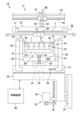
- FIG. 1 is a schematic diagram showing a board production system according to an embodiment
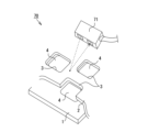
- FIG. 2 is a perspective view showing a substrate and a metal mask.
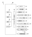
- 2 is a block diagram showing an electrical configuration of the board production system
- FIG. 13 is an image diagram showing a state in which the size of the gap between a metal mask and a substrate is measured.
- FIG. 13 is an image diagram showing a state in which solder paste is three-dimensionally measured.
- the association information may be information that associates the inspection results of the adhesion and the size of the mask opening with the inspection results of the printing state.
- the control device may determine whether the adhesion between the mask and the board is good or bad based on the association information, the inspection results obtained by the adhesion inspection device, and the size of the mask opening. By associating the size of the mask opening, the quality of the adhesion between the mask and the board can be suitably determined.
- the association information may be information that associates the inspection result of the printing state with at least one condition selected from the inspection result of the degree of adhesion, the size of the mask opening, and the printing conditions when printing the solder paste, the environmental conditions, and the clamping conditions related to the pressure for clamping the board.
- the control device may further derive the optimal printing conditions, environmental conditions, or clamping conditions for the degree of adhesion based on the association information and the result of the pass/fail judgment. According to this configuration, by associating the printing conditions, the printing conditions can be derived based on the result of the pass/fail judgment of the degree of adhesion between the mask and the board.
- the control device may determine the amount of board lift from the result of the pass/fail judgment, and may derive optimal printing conditions, environmental conditions, or clamp conditions for the determined amount of board lift, or may control each device to automatically set the determined amount of board lift and the derived conditions and perform printing.
- the amount of board lift determined from the result of the pass/fail judgment and the derived conditions are automatically set, making it easy to perform various adjustments before printing.
- the control device may instruct printing of solder paste on the board when it determines that a good print result can be obtained, but may eject the board without instructing printing of solder paste on the board or may stop due to an error when it determines that a good print result cannot be obtained.
- the board production system 10 of the present embodiment is a system that mounts components on a board 1 on which solder paste has been printed to produce a component-mounted board.
- the board production system 10 includes a screen printer 11 and a component mounter (not shown).
- the screen printer 11 is a device that prints solder paste on the board 1 and conveys the board 1 after the solder paste printing to the component mounter.
- the component mounter is a device that mounts components on the board 1 and conveys the board 1 after the components are mounted outside the board production system 10. Examples of components include semiconductor packages such as QFP (Quad Flat Package) and BGA (Ball Grid Array), and chip components such as chip resistors and chip capacitors.
- the screen printing machine 11 is equipped with a mask holding device 20, a substrate pressing device 50, and a squeegee device 60.
- the mask holding device 20 holds a metal mask 2 having a substantially square mask opening 3 (see FIG. 2).
- the mask holding device 20 holds the metal mask 2 in a mask holder 22 via a rectangular frame body 21.
- the metal mask 2 in this embodiment is a mask for solder paste printing.
- the board transport device 23 is a device that performs the tasks of transporting the board 1 to a working position within the screen printing machine 11, positioning the board 1 at the working position before solder paste printing, and transporting the board 1 from the working position after solder paste printing.
- the board transport device 23 can be composed of a pair of belt conveyors 26, a support device (not shown) that is attached to the belt conveyors 26 and supports the board 1 from below, and a drive device (not shown) that drives the belt conveyor 26.
- the clamping device 24 is a device for clamping the substrate 1.
- the clamping device 24 includes a pair of side frames 27 and a support base 28 that supports both side frames 27.
- a ball screw mechanism 29 is provided on one side frame 27 (the right side in FIG. 1), and the distance between the side frame 27 and the other side frame 27 (the left side in FIG. 1) can be adjusted by driving a clamping motor 30 (see FIG. 3).
- Clamping parts 31 are attached to the upper end surfaces of both side frames 27, and the clamping parts 31 approach each other to grip the substrate 1.
- a pair of belt conveyors 26 of the substrate transport device 23 are disposed inside both side frames 27.
- the support base 28 is supported via a ball screw mechanism (not shown) and is configured to be raised and lowered by a lifting motor 32.
- the lifting device 25 has a lifting platform 34 that rises and falls along a guide rail 33 extending vertically, and the lifting platform 34 is connected to a lifting motor 36 via a ball screw mechanism 35.
- the substrate transport device 23, clamp device 24, etc. are mounted on the lifting platform 34 via a support platform 37.
- a pair of mask supports 38 are provided on the support platform 37, and a mask support plate 39 that supports the metal mask 2 is fixed to the upper end surfaces of both mask supports 38.
- a ball screw mechanism 40 is configured on one mask support 38 (the right one in FIG. 1), and the distance to the other mask support 38 (the left one in FIG. 1) can be adjusted by driving a mask support motor 41 (see FIG. 3).
- the substrate pressing device 50 is a device that lifts the supported substrate 1 and presses the substrate 1 against the metal mask 2 from below.
- the substrate pressing device 50 is disposed between a pair of side frames 27 of the clamp device 24.
- a backup table 52 equipped with multiple backup pins 51 is supported via a ball screw mechanism 53, and the backup table 52 is configured to be raised and lowered by a backup motor 54.
- a camera C1 that can move in a planar direction is provided between the mask holder 22 and the clamp device 24.
- the camera C1 captures an image of a mark (not shown) on the substrate 1
- the amount of relative positional deviation in the planar direction between the substrate 1 and the metal mask 2 is calculated.
- a correction device (not shown) provided on the support base 37 corrects the positional deviation.
- the squeegee device 60 is also installed above the mask holder 22.
- the squeegee device 60 spreads the solder paste onto the metal mask 2, thereby transferring the solder paste to the portion of the substrate 1 that corresponds to the mask opening 3 (see FIG. 2).
- the squeegee device 60 is equipped with a running platform 61, on which a pair of squeegees 62 are mounted so that they can be raised and lowered.
- the running platform 61 is slidably attached to a guide rod 63, and can move linearly by being driven by a squeegee motor 65 (see FIG. 3) via a ball screw mechanism consisting of a screw shaft 64 arranged parallel to the guide rod 63.
- the screen printing machine 11 also includes an adhesion inspection device 70 (see Figs. 2 and 3) and a print inspection device 80 (see Fig. 3).
- the adhesion inspection device 70 is a device that measures the size of the gap between the metal mask 2 and the substrate 1 to inspect (measure) the adhesion between the metal mask 2 and the substrate 1. Specifically, before printing the solder paste, the adhesion inspection device 70 raises the substrate 1 to a printing position where it contacts the metal mask 2, and measures the size of the gap between the metal mask 2 and the substrate 1.
- the adhesion inspection device 70 of this embodiment also includes a laser displacement sensor 71.
- the laser displacement sensor 71 is mounted on the running platform 61 of the squeegee device 60.
- the laser displacement sensor 71 is a sensor that measures the top surface height of the substrate 1, the metal mask 2, etc. without contact.
- the print inspection device 80 is a device that performs three-dimensional measurement of the solder paste printed on the substrate 1 to inspect the printing condition of the solder paste.
- a scanning laser probe type non-contact three-dimensional measuring machine is used as the print inspection device 80.
- the print inspection device 80 is mounted inside the screen printing machine 11, specifically, to the side of the camera C1.
- the print inspection device 80 inspects the solder transfer condition, such as the volume and area (bleed) of the solder paste after printing.
- the board production system 10 is equipped with a control device 90.
- the control device 90 is a computer that includes a CPU 91, a ROM 92, a RAM 93, a memory 94, and an input/output interface 95.
- the ROM 92 stores a basic program for supplying solder paste to the board 1.
- the memory 94 stores a printing control program for the screen printer 11, etc.
- a touch panel display device 96 is also connected to the control device 90, allowing the worker to input data and display the details of the work.
- the laser displacement sensor 71 of the adhesion inspection device 70, the print inspection device 80, and the camera C1 are also connected to the control device 90.
- the motors 30 and 32 of the clamp device 24, the motors 36 and 41 of the lifting device 25, the motor 54 of the board pressing device 50, and the motor 65 of the squeegee device 60 are also connected to the control device 90.
- the belt conveyor 26 transports the substrate 1 between the pair of side frames 27.
- the backup motor 54 is then driven to raise the backup table 52, and the substrate 1 is lifted from the belt conveyor 26 by the multiple backup pins 51.
- the clamp motor 30 is then driven to move both side frames 27 in directions approaching each other, so that the substrate 1 is sandwiched and held between the pair of clamp sections 31.
- the lift motor 32 is driven to raise the clamp device 24 holding the substrate 1, so that the upper surface of the clamp part 31 and the upper surface of the substrate 1 are aligned with the upper surface of the mask support plate 39. Furthermore, the lift motor 36 is driven to raise the lift platform 34 and push up the substrate 1, so that the substrate 1 is pressed against the metal mask 2 from below.
- the CPU 91 of the control device 90 first measures the size of the gap between the metal mask 2 and the substrate 1 and performs a process (adhesion inspection step) to inspect the adhesion between the metal mask 2 and the substrate 1.
- the measurement of the size of the gap is performed by turning on the start button displayed on the display device 96. First, as shown in FIG.
- the height of the substrate 1 and metal mask 2 is measured using the laser displacement sensor 71.
- the laser displacement sensor 71 moves together with the running platform 61 of the squeegee device 60, and laser light is continuously irradiated onto the metal mask 2.
- the distance from the laser displacement sensor 71 to the top surface of the substrate 1 (land 4) (substrate top surface distance L1) and the distance from the laser displacement sensor 71 to the top surface of the metal mask 2 (mask top surface distance L2) are acquired as a set of measurement data (see FIG. 4).
- the size X of the gap between the metal mask 2 and the substrate 1 is calculated based on the distances L1 and L2, and the thickness C of the metal mask 2 input from the display device 96. Specifically, first, the top surface distance B is calculated by calculating the difference between the substrate top surface distance L1 and the mask top surface distance L2. Then, the size X of the gap is calculated based on the formula (top surface distance B - thickness C). The calculation of size X is performed at multiple points on the substrate 1.
- the CPU 91 drives the squeegee device 60 to spread the solder paste over the metal mask 2 and to push the solder paste into the mask openings 3 (see FIG. 2) of the metal mask 2. As a result, the solder paste is transferred onto the lands 4 formed in the parts of the substrate 1 that correspond to the mask openings 3.
- the print inspection device 80 is used to perform three-dimensional measurement of the solder paste printed on the board 1.
- the print inspection device 80 moves together with the camera C1, and the printed solder paste is continuously irradiated with laser light L3 (see FIG. 5).
- the three-dimensional shape of the printed solder paste is acquired as three-dimensional shape data.
- the print inspection device 80 then inspects the printing state of the three-dimensionally measured solder paste. Specifically, the print inspection device 80 inspects the solder transfer state, such as the volume of the solder bumps 5 and the area (bleed) of the printed solder paste, based on the acquired three-dimensional shape data. As a result, the volume and area of the printed solder paste are acquired as inspection data.
- the lifting motors 32 and 36 are driven to lower the board 1 for plate separation.
- the belt conveyor 26 is then driven to transport the board 1 out of the screen printing machine 11. Furthermore, the printed board 1 is transported into a component mounter, where components are mounted on the board 1 to produce a component-mounted board.
- association information that associates the adhesion inspection results (size of gaps X at multiple locations on substrate 1) with the print state inspection results (volume and area of printed solder paste) is stored in RAM 93 (information storage step).
- RAM 93 functions as a storage device that stores association information.
- RAM 93 also stores associated printing conditions (printing speed, printing pressure, plate release conditions, etc.) and environmental conditions (remaining amount of solder, atmospheric temperature and humidity, cleaning timing, etc.).
- the CPU 91 When the association information is stored in the RAM 93 by the above method, the CPU 91 further executes a judgment step for the next board 1 to be produced. That is, in the same manner as the above method, when a new board 1 is brought into the screen printing machine 11 and the newly brought-in board 1 is pressed against the metal mask 2 from below (i.e., when the position (H1) of the top surface of the board 1 is positioned at the printing reference height (H0)), a process (adhesion inspection step) is first executed to inspect the adhesion between the metal mask 2 and the board 1.
- the CPU 91 judges whether the adhesion between the metal mask 2 and the board 1 is good or bad based on the association information stored in the RAM 93 and the inspection result obtained by the adhesion inspection device 70. Then, the CPU 91 causes the display device 96 to display (present) the result of the pass/fail judgment. Furthermore, the CPU 91 further derives the optimal printing conditions and environmental conditions for the adhesion based on the association information and the result of the pass/fail judgment. Specifically, the CPU 91 determines the amount of substrate lift (amount of pressure applied to the metal mask 2) from the pass/fail judgment results, and derives optimal printing conditions and environmental conditions for the determined amount of substrate lift.
- the determined amount of substrate lift and the derived conditions are displayed on the display device 96. After checking the displayed contents, the worker sets a new amount of substrate lift and the derived conditions (printing conditions and environmental conditions) displayed on the display device 96. Thus, the amount of substrate lift, printing conditions, and environmental conditions are adjusted until good printing results are obtained.
- the CPU 91 causes the display device 96 to display (present) a message indicating that the board lift amount should be increased, for example, by 0.15 mm so that the gap is less than 0.1 mm.
- a new board lift amount is set by the operator, and if it is determined that good printing results can be obtained, the CPU 91 instructs printing of solder paste on the board 1. However, if it is determined that good printing results cannot be obtained, the CPU 91 does not instruct printing of solder paste on the board 1 and ejects the board 1 from the board production system 10.
- the optimal printing conditions and environmental conditions for the determined amount of substrate lift may be derived based on the three-dimensional measurement results obtained in the print inspection step.
- the RAM 93 stores association information that associates the results of the adhesion inspection (the size of the gap X at multiple locations on the substrate 1), the results of the print state inspection (the volume and area of the printed solder paste), the printing conditions (printing speed, printing pressure, plate release conditions, etc.), and the environmental conditions (residual amount of solder, atmospheric temperature and humidity, cleaning time, etc.).
- the association information stored in the RAM 93 is extracted from the association information obtained when printing is performed with the same amount of substrate lift as the determined amount of substrate lift. Then, from the extracted association information, the one that provides the optimal print result (i.e., the three-dimensional measurement result) is selected, and the printing conditions and environmental conditions are derived from the selected association information. For example, when the amount of substrate lift is determined, the CPU 91 searches for association information stored in the RAM 93, extracts association information that matches the amount of substrate lift, and outputs a list of printing conditions and environmental conditions in order of best printing results. The CPU 91 (or the user) then determines the printing conditions and environmental conditions from the list of printing conditions and environmental conditions that has been output.
- the printing conditions and environmental conditions may be changed without changing the substrate lift amount (substrate pressing amount). If it is possible to reduce the gap X by changing the printing conditions and environmental conditions, for example, the printing inspection data when the gap X is reduced by changing the printing conditions and environmental conditions without changing the substrate lift amount (substrate pressing amount) may be compared with the printing inspection data when the substrate lift amount (substrate pressing amount) is changed (but the gap X does not change) and the printing conditions and environmental conditions are changed, and the conditions that provide better quality may be adopted.
- association information for substrates of different sizes may be added to the data for determining the substrate lift amount, printing conditions, and environmental conditions. As described above, whether to change the substrate lift amount, the printing conditions, and environmental conditions, or both the substrate lift amount and the printing conditions and environmental conditions can be determined based on the association information stored in the RAM 93 so as to obtain the optimal printing result.
- association information that associates the adhesion inspection results by the adhesion inspection device 70 with the print state inspection results by the print inspection device 80 is stored. This clarifies the relationship between the adhesion between the metal mask 2 and the board 1 and the quality of the printed state of the solder paste (whether there is a printing defect such as bleeding). Then, when printing on a new board 1, the quality of the adhesion between the metal mask 2 and the board 1 is judged based on the stored association information and the inspection results obtained by the adhesion inspection device 70. Therefore, based on the result of the judgment of the quality of the adhesion (the gap between the metal mask 2 and the board 1), printing conditions (for example, the amount of board lift (amount of pressing against the metal mask 2)) for reducing print defects can be determined.
- the association information is information that associates the adhesion inspection result with the print state inspection result, and the CPU 91 judges the quality of the adhesion between the metal mask 2 and the substrate 1 from the association information and the inspection result obtained by the adhesion inspection device 70, but the configuration is not limited to this.
- the association information may be information that associates the adhesion inspection result, the size (or approximate size) of the mask opening 3, and the inspection result of the print state, and the CPU 91 may judge the quality of the adhesion between the metal mask 2 and the substrate 1 from the association information, the inspection result obtained by the adhesion inspection device 70, and the size (or approximate size) of the mask opening 3.
- the CPU 91 may then determine the amount of substrate lift from the result of the quality judgment, and display (present) the determined amount of substrate lift on the display device 96.
- association information indicating that a defect (bleed) will occur at a square mask opening 3 with a side length of 0.6 mm when the gap is 0.15 mm or more and association information indicating that a transfer defect will occur at a circular mask opening with an inner diameter of 0.3 mm when the gap is 0.05 mm or more are stored in the RAM 93.
- the CPU 91 may display (present) on the display device 96 that the substrate lift amount should be increased by, for example, 0.08 mm so that the gap near the circular mask opening becomes less than 0.05 mm.
- the association information is information that associates the adhesion inspection result with the print state inspection result, and the CPU 91 judges the quality of the adhesion between the metal mask 2 and the substrate 1 based on the association information and the inspection result obtained by the adhesion inspection device 70, but this configuration is not limited to this.
- the association information may be information that associates the adhesion inspection result, the size of the mask opening 3, and at least one condition selected from the printing conditions when printing the solder paste, the environmental conditions, and the clamping conditions related to the pressure for clamping the substrate 1, with the print state inspection result.
- the CPU 91 may further derive the optimal printing conditions, environmental conditions, or clamping conditions for the adhesion based on the association information and the result of the judgment of the quality of the adhesion. The CPU 91 may then determine the amount of substrate lift from the result of the quality judgment, and derive the optimal printing conditions, environmental conditions, or clamping conditions when the substrate is lifted to the determined amount, or control each device to automatically set the determined substrate lift amount and the derived conditions and perform printing.
- the CPU 91 displays (presents) the determined substrate lift amount on the display device 96, and the operator sets the substrate lift amount after checking the displayed content, but this configuration is not limited to this.
- the CPU 91 may automatically set the determined substrate lift amount and perform printing.
- the mask opening 3 is substantially square-shaped, but is not limited to this configuration.
- the mask opening 3 may be other shapes, such as rectangular, circular, or elliptical.
- a scanning laser probe type non-contact three-dimensional measuring machine was used as the print inspection device 80, but this configuration is not limited to this.
- an optical type non-contact three-dimensional measuring machine may be used as the print inspection device 80.
- the adhesion inspection device 70 and the print inspection device 80 are installed inside the screen printing machine 11, but this configuration is not limited to this.
- the print inspection device 80 may be installed in a location separate from the screen printing machine 11, next to the screen printing machine 11 in the board production system 10.
- the CPU 91 ejects the substrate 1 from the substrate production system 10 without instructing printing of solder paste on the substrate 1, but this configuration is not limited to this.
- the CPU 91 may stop the substrate 1 due to an error without instructing printing of solder paste on the substrate 1.
- Substrate 2 Metal mask as a mask 3: Mask opening 10: Substrate production system 20: Mask holding device 50: Substrate pressing device 60: Squeegee device 70: Adhesion inspection device 80: Print inspection device 90: Control device 93: RAM as a storage device
Landscapes
- Engineering & Computer Science (AREA)
- Manufacturing & Machinery (AREA)
- Microelectronics & Electronic Packaging (AREA)
- Electric Connection Of Electric Components To Printed Circuits (AREA)
- Screen Printers (AREA)
Abstract
La présente invention concerne un système de production de substrat qui comprend un dispositif de pressage de substrat, un dispositif de raclage, un dispositif d'inspection d'adhérence, un dispositif d'inspection d'impression et un dispositif de commande. Le dispositif de pressage de substrat soulève un substrat et presse le substrat, par le dessous, contre un masque. Le dispositif de raclage étale une pâte à braser sur le masque, transférant ainsi la pâte à braser à une section correspondant à une ouverture de masque sur le substrat. Le dispositif d'inspection d'adhérence mesure la taille d'un espace entre le masque et le substrat, et inspecte l'adhérence entre le masque et le substrat. Le dispositif d'inspection d'impression mesure en trois dimensions la pâte à braser imprimée sur le substrat, et inspecte l'état d'impression de la pâte à braser. Le dispositif de commande détermine l'adéquation de l'adhérence entre le masque et le substrat sur la base : d'informations d'association associant les résultats d'inspection d'adhérence et les résultats d'inspection d'état d'impression ; et des résultats d'inspection obtenus par le dispositif d'inspection d'adhérence.
Priority Applications (2)
| Application Number | Priority Date | Filing Date | Title |
|---|---|---|---|
| CN202380100945.8A CN121605757A (zh) | 2023-08-23 | 2023-08-23 | 基板生产系统及基板生产方法 |
| PCT/JP2023/030250 WO2025041289A1 (fr) | 2023-08-23 | 2023-08-23 | Système de production de substrat et procédé de production de substrat |
Applications Claiming Priority (1)
| Application Number | Priority Date | Filing Date | Title |
|---|---|---|---|
| PCT/JP2023/030250 WO2025041289A1 (fr) | 2023-08-23 | 2023-08-23 | Système de production de substrat et procédé de production de substrat |
Publications (1)
| Publication Number | Publication Date |
|---|---|
| WO2025041289A1 true WO2025041289A1 (fr) | 2025-02-27 |
Family
ID=94731763
Family Applications (1)
| Application Number | Title | Priority Date | Filing Date |
|---|---|---|---|
| PCT/JP2023/030250 Pending WO2025041289A1 (fr) | 2023-08-23 | 2023-08-23 | Système de production de substrat et procédé de production de substrat |
Country Status (2)
| Country | Link |
|---|---|
| CN (1) | CN121605757A (fr) |
| WO (1) | WO2025041289A1 (fr) |
Citations (3)
| Publication number | Priority date | Publication date | Assignee | Title |
|---|---|---|---|---|
| JP2000190452A (ja) * | 1998-12-25 | 2000-07-11 | Matsushita Electric Ind Co Ltd | クリ―ム半田印刷機 |
| JP2002029034A (ja) * | 2000-07-18 | 2002-01-29 | Matsushita Electric Ind Co Ltd | スクリーン印刷装置およびスクリーン印刷方法 |
| JP2012158129A (ja) * | 2011-02-02 | 2012-08-23 | Panasonic Corp | スクリーン印刷装置およびスクリーン印刷方法 |
-
2023
- 2023-08-23 CN CN202380100945.8A patent/CN121605757A/zh active Pending
- 2023-08-23 WO PCT/JP2023/030250 patent/WO2025041289A1/fr active Pending
Patent Citations (3)
| Publication number | Priority date | Publication date | Assignee | Title |
|---|---|---|---|---|
| JP2000190452A (ja) * | 1998-12-25 | 2000-07-11 | Matsushita Electric Ind Co Ltd | クリ―ム半田印刷機 |
| JP2002029034A (ja) * | 2000-07-18 | 2002-01-29 | Matsushita Electric Ind Co Ltd | スクリーン印刷装置およびスクリーン印刷方法 |
| JP2012158129A (ja) * | 2011-02-02 | 2012-08-23 | Panasonic Corp | スクリーン印刷装置およびスクリーン印刷方法 |
Also Published As
| Publication number | Publication date |
|---|---|
| CN121605757A (zh) | 2026-03-03 |
Similar Documents
| Publication | Publication Date | Title |
|---|---|---|
| KR20120049172A (ko) | 스크린 인쇄 장치 및 스크린 인쇄 방법 | |
| EP1076480B1 (fr) | Procédé et dispositif d'impression par masque | |
| CN112334313B (zh) | 丝网印刷装置以及丝网印刷方法 | |
| JP2007173552A (ja) | 電子部品実装システムおよび電子部品実装方法 | |
| JP2007320207A (ja) | スクリーン印刷方法及びスクリーン印刷装置 | |
| JP7086862B2 (ja) | スクリーン印刷機 | |
| CN110637508A (zh) | 测定位置决定装置 | |
| JP4237158B2 (ja) | 実装基板製造装置および製造方法 | |
| JP2008198730A (ja) | 表面実装機、スクリーン印刷装置及び実装ライン | |
| JP3750484B2 (ja) | スクリーン印刷方法 | |
| US20230014796A1 (en) | Screen mask inspection device, solder printing inspection device, and method for inspecting screen mask | |
| JP6694778B2 (ja) | スクリーン印刷装置 | |
| JP5739754B2 (ja) | 電子回路部品の立上がり防止方法および電子回路製造システム | |
| JP3758463B2 (ja) | スクリーン印刷の検査方法 | |
| WO2025041289A1 (fr) | Système de production de substrat et procédé de production de substrat | |
| JP3692912B2 (ja) | スクリーン印刷方法 | |
| CN111093996B (zh) | 丝网印刷机 | |
| JP5487982B2 (ja) | スクリーン印刷機及びスクリーン印刷機の異物検出方法 | |
| JP2004042334A (ja) | スクリーン印刷機 | |
| JP2002029027A (ja) | スクリーン印刷装置およびスクリーン印刷方法 | |
| JP7458488B2 (ja) | 印刷品質管理システムおよび印刷品質管理方法 | |
| JP7796362B1 (ja) | ワーク処理装置およびワーク処理方法 | |
| JP7389894B2 (ja) | 印刷機および印刷システム | |
| JP7629465B2 (ja) | 対基板作業機、および演算方法 | |
| JP4954666B2 (ja) | 実装機およびこれを用いた部品実装システム |
Legal Events
| Date | Code | Title | Description |
|---|---|---|---|
| 121 | Ep: the epo has been informed by wipo that ep was designated in this application |
Ref document number: 23949749 Country of ref document: EP Kind code of ref document: A1 |
|
| ENP | Entry into the national phase |
Ref document number: 2025541236 Country of ref document: JP Kind code of ref document: A |
|
| WWE | Wipo information: entry into national phase |
Ref document number: 2025541236 Country of ref document: JP |