WO2025041289A1 - Substrate production system and substrate production method - Google Patents
Substrate production system and substrate production method Download PDFInfo
- Publication number
- WO2025041289A1 WO2025041289A1 PCT/JP2023/030250 JP2023030250W WO2025041289A1 WO 2025041289 A1 WO2025041289 A1 WO 2025041289A1 JP 2023030250 W JP2023030250 W JP 2023030250W WO 2025041289 A1 WO2025041289 A1 WO 2025041289A1
- Authority
- WO
- WIPO (PCT)
- Prior art keywords
- substrate
- mask
- printing
- adhesion
- board
- Prior art date
- Legal status (The legal status is an assumption and is not a legal conclusion. Google has not performed a legal analysis and makes no representation as to the accuracy of the status listed.)
- Pending
Links
Images


Classifications
-
- H—ELECTRICITY
- H05—ELECTRIC TECHNIQUES NOT OTHERWISE PROVIDED FOR
- H05K—PRINTED CIRCUITS; CASINGS OR CONSTRUCTIONAL DETAILS OF ELECTRIC APPARATUS; MANUFACTURE OF ASSEMBLAGES OF ELECTRICAL COMPONENTS
- H05K3/00—Apparatus or processes for manufacturing printed circuits
- H05K3/10—Apparatus or processes for manufacturing printed circuits in which conductive material is applied to the insulating support in such a manner as to form the desired conductive pattern
- H05K3/12—Apparatus or processes for manufacturing printed circuits in which conductive material is applied to the insulating support in such a manner as to form the desired conductive pattern using thick film techniques, e.g. printing techniques to apply the conductive material or similar techniques for applying conductive paste or ink patterns
Definitions
- the technology disclosed in this specification relates to a board production system and a board production method.
- board production systems that include a screen printer and a component mounter are well known.
- a screen printer usually prints solder paste onto a board, and then a component mounter mounts components onto the board, producing a component-mounted board.
- the gap that occurs between the mask (screen mask) and the substrate during paste printing is one of the factors that greatly affect the quality of printing. For example, if the gap is larger than the paste particles, the pressure applied when filling the mask opening with solder paste causes the solder paste to enter the gap and cause bleeding. In this case, printing of a good shape cannot be performed.
- the gap between the mask and the substrate occurs due to thickness errors, surface irregularities, warping, etc. of the substrate. Therefore, as a device for checking such gaps, a technology has been proposed in the past that lifts the substrate to a printing position input in advance before paste printing and measures the size of the gap between the mask and the substrate.
- Patent Document 1 Publication WO2019/049278
- This specification therefore provides a technique for clarifying the relationship between the degree of adhesion between the mask and the substrate and the quality of the printing condition of the solder paste.
- the board production system includes a mask holding device, a board pressing device, a squeegee device, an adhesion inspection device, a print inspection device, a storage device, and a control device.
- the mask holding device holds a mask having a mask opening.
- the board pressing device lifts the supported board and presses the board against the mask from below.
- the squeegee device spreads the solder paste on the mask to transfer the solder paste to the part of the board that corresponds to the mask opening.
- the adhesion inspection device measures the size of the gap between the mask and the board to inspect the adhesion between the mask and the board.
- the print inspection device performs three-dimensional measurement of the solder paste printed on the board to inspect the printing condition of the solder paste.
- the storage device stores association information that associates the adhesion inspection results with the printing condition inspection results.
- the control device judges whether the adhesion between the mask and the board is good or bad based on the association information stored in the storage device and the inspection results obtained by the adhesion inspection device. Therefore, with the above-mentioned configuration, it is possible to clarify the relationship between the degree of adhesion between the mask and the substrate and the quality of the printing condition of the solder paste.
- the board production method includes an adhesion inspection step, a printing inspection step, an information storage step, and a judgment step.
- the adhesion inspection step the size of the gap between a mask for printing solder paste and the board is measured to inspect the adhesion between the mask and the board.
- the printing inspection step the solder paste printed on the board is measured in three dimensions to inspect the printing condition of the solder paste.
- the information storage step information correlating the adhesion inspection results with the inspection results of the printing condition is stored.
- the judgment step the quality of the adhesion between the mask and the board is judged based on the associated information and the inspection results obtained by the adhesion inspection device.
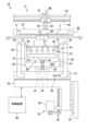
- FIG. 1 is a schematic diagram showing a board production system according to an embodiment
- FIG. 2 is a perspective view showing a substrate and a metal mask.
- 2 is a block diagram showing an electrical configuration of the board production system
- FIG. 13 is an image diagram showing a state in which the size of the gap between a metal mask and a substrate is measured.
- FIG. 13 is an image diagram showing a state in which solder paste is three-dimensionally measured.
- the association information may be information that associates the inspection results of the adhesion and the size of the mask opening with the inspection results of the printing state.
- the control device may determine whether the adhesion between the mask and the board is good or bad based on the association information, the inspection results obtained by the adhesion inspection device, and the size of the mask opening. By associating the size of the mask opening, the quality of the adhesion between the mask and the board can be suitably determined.
- the association information may be information that associates the inspection result of the printing state with at least one condition selected from the inspection result of the degree of adhesion, the size of the mask opening, and the printing conditions when printing the solder paste, the environmental conditions, and the clamping conditions related to the pressure for clamping the board.
- the control device may further derive the optimal printing conditions, environmental conditions, or clamping conditions for the degree of adhesion based on the association information and the result of the pass/fail judgment. According to this configuration, by associating the printing conditions, the printing conditions can be derived based on the result of the pass/fail judgment of the degree of adhesion between the mask and the board.
- the control device may determine the amount of board lift from the result of the pass/fail judgment, and may derive optimal printing conditions, environmental conditions, or clamp conditions for the determined amount of board lift, or may control each device to automatically set the determined amount of board lift and the derived conditions and perform printing.
- the amount of board lift determined from the result of the pass/fail judgment and the derived conditions are automatically set, making it easy to perform various adjustments before printing.
- the control device may instruct printing of solder paste on the board when it determines that a good print result can be obtained, but may eject the board without instructing printing of solder paste on the board or may stop due to an error when it determines that a good print result cannot be obtained.
- the board production system 10 of the present embodiment is a system that mounts components on a board 1 on which solder paste has been printed to produce a component-mounted board.
- the board production system 10 includes a screen printer 11 and a component mounter (not shown).
- the screen printer 11 is a device that prints solder paste on the board 1 and conveys the board 1 after the solder paste printing to the component mounter.
- the component mounter is a device that mounts components on the board 1 and conveys the board 1 after the components are mounted outside the board production system 10. Examples of components include semiconductor packages such as QFP (Quad Flat Package) and BGA (Ball Grid Array), and chip components such as chip resistors and chip capacitors.
- the screen printing machine 11 is equipped with a mask holding device 20, a substrate pressing device 50, and a squeegee device 60.
- the mask holding device 20 holds a metal mask 2 having a substantially square mask opening 3 (see FIG. 2).
- the mask holding device 20 holds the metal mask 2 in a mask holder 22 via a rectangular frame body 21.
- the metal mask 2 in this embodiment is a mask for solder paste printing.
- the board transport device 23 is a device that performs the tasks of transporting the board 1 to a working position within the screen printing machine 11, positioning the board 1 at the working position before solder paste printing, and transporting the board 1 from the working position after solder paste printing.
- the board transport device 23 can be composed of a pair of belt conveyors 26, a support device (not shown) that is attached to the belt conveyors 26 and supports the board 1 from below, and a drive device (not shown) that drives the belt conveyor 26.
- the clamping device 24 is a device for clamping the substrate 1.
- the clamping device 24 includes a pair of side frames 27 and a support base 28 that supports both side frames 27.
- a ball screw mechanism 29 is provided on one side frame 27 (the right side in FIG. 1), and the distance between the side frame 27 and the other side frame 27 (the left side in FIG. 1) can be adjusted by driving a clamping motor 30 (see FIG. 3).
- Clamping parts 31 are attached to the upper end surfaces of both side frames 27, and the clamping parts 31 approach each other to grip the substrate 1.
- a pair of belt conveyors 26 of the substrate transport device 23 are disposed inside both side frames 27.
- the support base 28 is supported via a ball screw mechanism (not shown) and is configured to be raised and lowered by a lifting motor 32.
- the lifting device 25 has a lifting platform 34 that rises and falls along a guide rail 33 extending vertically, and the lifting platform 34 is connected to a lifting motor 36 via a ball screw mechanism 35.
- the substrate transport device 23, clamp device 24, etc. are mounted on the lifting platform 34 via a support platform 37.
- a pair of mask supports 38 are provided on the support platform 37, and a mask support plate 39 that supports the metal mask 2 is fixed to the upper end surfaces of both mask supports 38.
- a ball screw mechanism 40 is configured on one mask support 38 (the right one in FIG. 1), and the distance to the other mask support 38 (the left one in FIG. 1) can be adjusted by driving a mask support motor 41 (see FIG. 3).
- the substrate pressing device 50 is a device that lifts the supported substrate 1 and presses the substrate 1 against the metal mask 2 from below.
- the substrate pressing device 50 is disposed between a pair of side frames 27 of the clamp device 24.
- a backup table 52 equipped with multiple backup pins 51 is supported via a ball screw mechanism 53, and the backup table 52 is configured to be raised and lowered by a backup motor 54.
- a camera C1 that can move in a planar direction is provided between the mask holder 22 and the clamp device 24.
- the camera C1 captures an image of a mark (not shown) on the substrate 1
- the amount of relative positional deviation in the planar direction between the substrate 1 and the metal mask 2 is calculated.
- a correction device (not shown) provided on the support base 37 corrects the positional deviation.
- the squeegee device 60 is also installed above the mask holder 22.
- the squeegee device 60 spreads the solder paste onto the metal mask 2, thereby transferring the solder paste to the portion of the substrate 1 that corresponds to the mask opening 3 (see FIG. 2).
- the squeegee device 60 is equipped with a running platform 61, on which a pair of squeegees 62 are mounted so that they can be raised and lowered.
- the running platform 61 is slidably attached to a guide rod 63, and can move linearly by being driven by a squeegee motor 65 (see FIG. 3) via a ball screw mechanism consisting of a screw shaft 64 arranged parallel to the guide rod 63.
- the screen printing machine 11 also includes an adhesion inspection device 70 (see Figs. 2 and 3) and a print inspection device 80 (see Fig. 3).
- the adhesion inspection device 70 is a device that measures the size of the gap between the metal mask 2 and the substrate 1 to inspect (measure) the adhesion between the metal mask 2 and the substrate 1. Specifically, before printing the solder paste, the adhesion inspection device 70 raises the substrate 1 to a printing position where it contacts the metal mask 2, and measures the size of the gap between the metal mask 2 and the substrate 1.
- the adhesion inspection device 70 of this embodiment also includes a laser displacement sensor 71.
- the laser displacement sensor 71 is mounted on the running platform 61 of the squeegee device 60.
- the laser displacement sensor 71 is a sensor that measures the top surface height of the substrate 1, the metal mask 2, etc. without contact.
- the print inspection device 80 is a device that performs three-dimensional measurement of the solder paste printed on the substrate 1 to inspect the printing condition of the solder paste.
- a scanning laser probe type non-contact three-dimensional measuring machine is used as the print inspection device 80.
- the print inspection device 80 is mounted inside the screen printing machine 11, specifically, to the side of the camera C1.
- the print inspection device 80 inspects the solder transfer condition, such as the volume and area (bleed) of the solder paste after printing.
- the board production system 10 is equipped with a control device 90.
- the control device 90 is a computer that includes a CPU 91, a ROM 92, a RAM 93, a memory 94, and an input/output interface 95.
- the ROM 92 stores a basic program for supplying solder paste to the board 1.
- the memory 94 stores a printing control program for the screen printer 11, etc.
- a touch panel display device 96 is also connected to the control device 90, allowing the worker to input data and display the details of the work.
- the laser displacement sensor 71 of the adhesion inspection device 70, the print inspection device 80, and the camera C1 are also connected to the control device 90.
- the motors 30 and 32 of the clamp device 24, the motors 36 and 41 of the lifting device 25, the motor 54 of the board pressing device 50, and the motor 65 of the squeegee device 60 are also connected to the control device 90.
- the belt conveyor 26 transports the substrate 1 between the pair of side frames 27.
- the backup motor 54 is then driven to raise the backup table 52, and the substrate 1 is lifted from the belt conveyor 26 by the multiple backup pins 51.
- the clamp motor 30 is then driven to move both side frames 27 in directions approaching each other, so that the substrate 1 is sandwiched and held between the pair of clamp sections 31.
- the lift motor 32 is driven to raise the clamp device 24 holding the substrate 1, so that the upper surface of the clamp part 31 and the upper surface of the substrate 1 are aligned with the upper surface of the mask support plate 39. Furthermore, the lift motor 36 is driven to raise the lift platform 34 and push up the substrate 1, so that the substrate 1 is pressed against the metal mask 2 from below.
- the CPU 91 of the control device 90 first measures the size of the gap between the metal mask 2 and the substrate 1 and performs a process (adhesion inspection step) to inspect the adhesion between the metal mask 2 and the substrate 1.
- the measurement of the size of the gap is performed by turning on the start button displayed on the display device 96. First, as shown in FIG.
- the height of the substrate 1 and metal mask 2 is measured using the laser displacement sensor 71.
- the laser displacement sensor 71 moves together with the running platform 61 of the squeegee device 60, and laser light is continuously irradiated onto the metal mask 2.
- the distance from the laser displacement sensor 71 to the top surface of the substrate 1 (land 4) (substrate top surface distance L1) and the distance from the laser displacement sensor 71 to the top surface of the metal mask 2 (mask top surface distance L2) are acquired as a set of measurement data (see FIG. 4).
- the size X of the gap between the metal mask 2 and the substrate 1 is calculated based on the distances L1 and L2, and the thickness C of the metal mask 2 input from the display device 96. Specifically, first, the top surface distance B is calculated by calculating the difference between the substrate top surface distance L1 and the mask top surface distance L2. Then, the size X of the gap is calculated based on the formula (top surface distance B - thickness C). The calculation of size X is performed at multiple points on the substrate 1.
- the CPU 91 drives the squeegee device 60 to spread the solder paste over the metal mask 2 and to push the solder paste into the mask openings 3 (see FIG. 2) of the metal mask 2. As a result, the solder paste is transferred onto the lands 4 formed in the parts of the substrate 1 that correspond to the mask openings 3.
- the print inspection device 80 is used to perform three-dimensional measurement of the solder paste printed on the board 1.
- the print inspection device 80 moves together with the camera C1, and the printed solder paste is continuously irradiated with laser light L3 (see FIG. 5).
- the three-dimensional shape of the printed solder paste is acquired as three-dimensional shape data.
- the print inspection device 80 then inspects the printing state of the three-dimensionally measured solder paste. Specifically, the print inspection device 80 inspects the solder transfer state, such as the volume of the solder bumps 5 and the area (bleed) of the printed solder paste, based on the acquired three-dimensional shape data. As a result, the volume and area of the printed solder paste are acquired as inspection data.
- the lifting motors 32 and 36 are driven to lower the board 1 for plate separation.
- the belt conveyor 26 is then driven to transport the board 1 out of the screen printing machine 11. Furthermore, the printed board 1 is transported into a component mounter, where components are mounted on the board 1 to produce a component-mounted board.
- association information that associates the adhesion inspection results (size of gaps X at multiple locations on substrate 1) with the print state inspection results (volume and area of printed solder paste) is stored in RAM 93 (information storage step).
- RAM 93 functions as a storage device that stores association information.
- RAM 93 also stores associated printing conditions (printing speed, printing pressure, plate release conditions, etc.) and environmental conditions (remaining amount of solder, atmospheric temperature and humidity, cleaning timing, etc.).
- the CPU 91 When the association information is stored in the RAM 93 by the above method, the CPU 91 further executes a judgment step for the next board 1 to be produced. That is, in the same manner as the above method, when a new board 1 is brought into the screen printing machine 11 and the newly brought-in board 1 is pressed against the metal mask 2 from below (i.e., when the position (H1) of the top surface of the board 1 is positioned at the printing reference height (H0)), a process (adhesion inspection step) is first executed to inspect the adhesion between the metal mask 2 and the board 1.
- the CPU 91 judges whether the adhesion between the metal mask 2 and the board 1 is good or bad based on the association information stored in the RAM 93 and the inspection result obtained by the adhesion inspection device 70. Then, the CPU 91 causes the display device 96 to display (present) the result of the pass/fail judgment. Furthermore, the CPU 91 further derives the optimal printing conditions and environmental conditions for the adhesion based on the association information and the result of the pass/fail judgment. Specifically, the CPU 91 determines the amount of substrate lift (amount of pressure applied to the metal mask 2) from the pass/fail judgment results, and derives optimal printing conditions and environmental conditions for the determined amount of substrate lift.
- the determined amount of substrate lift and the derived conditions are displayed on the display device 96. After checking the displayed contents, the worker sets a new amount of substrate lift and the derived conditions (printing conditions and environmental conditions) displayed on the display device 96. Thus, the amount of substrate lift, printing conditions, and environmental conditions are adjusted until good printing results are obtained.
- the CPU 91 causes the display device 96 to display (present) a message indicating that the board lift amount should be increased, for example, by 0.15 mm so that the gap is less than 0.1 mm.
- a new board lift amount is set by the operator, and if it is determined that good printing results can be obtained, the CPU 91 instructs printing of solder paste on the board 1. However, if it is determined that good printing results cannot be obtained, the CPU 91 does not instruct printing of solder paste on the board 1 and ejects the board 1 from the board production system 10.
- the optimal printing conditions and environmental conditions for the determined amount of substrate lift may be derived based on the three-dimensional measurement results obtained in the print inspection step.
- the RAM 93 stores association information that associates the results of the adhesion inspection (the size of the gap X at multiple locations on the substrate 1), the results of the print state inspection (the volume and area of the printed solder paste), the printing conditions (printing speed, printing pressure, plate release conditions, etc.), and the environmental conditions (residual amount of solder, atmospheric temperature and humidity, cleaning time, etc.).
- the association information stored in the RAM 93 is extracted from the association information obtained when printing is performed with the same amount of substrate lift as the determined amount of substrate lift. Then, from the extracted association information, the one that provides the optimal print result (i.e., the three-dimensional measurement result) is selected, and the printing conditions and environmental conditions are derived from the selected association information. For example, when the amount of substrate lift is determined, the CPU 91 searches for association information stored in the RAM 93, extracts association information that matches the amount of substrate lift, and outputs a list of printing conditions and environmental conditions in order of best printing results. The CPU 91 (or the user) then determines the printing conditions and environmental conditions from the list of printing conditions and environmental conditions that has been output.
- the printing conditions and environmental conditions may be changed without changing the substrate lift amount (substrate pressing amount). If it is possible to reduce the gap X by changing the printing conditions and environmental conditions, for example, the printing inspection data when the gap X is reduced by changing the printing conditions and environmental conditions without changing the substrate lift amount (substrate pressing amount) may be compared with the printing inspection data when the substrate lift amount (substrate pressing amount) is changed (but the gap X does not change) and the printing conditions and environmental conditions are changed, and the conditions that provide better quality may be adopted.
- association information for substrates of different sizes may be added to the data for determining the substrate lift amount, printing conditions, and environmental conditions. As described above, whether to change the substrate lift amount, the printing conditions, and environmental conditions, or both the substrate lift amount and the printing conditions and environmental conditions can be determined based on the association information stored in the RAM 93 so as to obtain the optimal printing result.
- association information that associates the adhesion inspection results by the adhesion inspection device 70 with the print state inspection results by the print inspection device 80 is stored. This clarifies the relationship between the adhesion between the metal mask 2 and the board 1 and the quality of the printed state of the solder paste (whether there is a printing defect such as bleeding). Then, when printing on a new board 1, the quality of the adhesion between the metal mask 2 and the board 1 is judged based on the stored association information and the inspection results obtained by the adhesion inspection device 70. Therefore, based on the result of the judgment of the quality of the adhesion (the gap between the metal mask 2 and the board 1), printing conditions (for example, the amount of board lift (amount of pressing against the metal mask 2)) for reducing print defects can be determined.
- the association information is information that associates the adhesion inspection result with the print state inspection result, and the CPU 91 judges the quality of the adhesion between the metal mask 2 and the substrate 1 from the association information and the inspection result obtained by the adhesion inspection device 70, but the configuration is not limited to this.
- the association information may be information that associates the adhesion inspection result, the size (or approximate size) of the mask opening 3, and the inspection result of the print state, and the CPU 91 may judge the quality of the adhesion between the metal mask 2 and the substrate 1 from the association information, the inspection result obtained by the adhesion inspection device 70, and the size (or approximate size) of the mask opening 3.
- the CPU 91 may then determine the amount of substrate lift from the result of the quality judgment, and display (present) the determined amount of substrate lift on the display device 96.
- association information indicating that a defect (bleed) will occur at a square mask opening 3 with a side length of 0.6 mm when the gap is 0.15 mm or more and association information indicating that a transfer defect will occur at a circular mask opening with an inner diameter of 0.3 mm when the gap is 0.05 mm or more are stored in the RAM 93.
- the CPU 91 may display (present) on the display device 96 that the substrate lift amount should be increased by, for example, 0.08 mm so that the gap near the circular mask opening becomes less than 0.05 mm.
- the association information is information that associates the adhesion inspection result with the print state inspection result, and the CPU 91 judges the quality of the adhesion between the metal mask 2 and the substrate 1 based on the association information and the inspection result obtained by the adhesion inspection device 70, but this configuration is not limited to this.
- the association information may be information that associates the adhesion inspection result, the size of the mask opening 3, and at least one condition selected from the printing conditions when printing the solder paste, the environmental conditions, and the clamping conditions related to the pressure for clamping the substrate 1, with the print state inspection result.
- the CPU 91 may further derive the optimal printing conditions, environmental conditions, or clamping conditions for the adhesion based on the association information and the result of the judgment of the quality of the adhesion. The CPU 91 may then determine the amount of substrate lift from the result of the quality judgment, and derive the optimal printing conditions, environmental conditions, or clamping conditions when the substrate is lifted to the determined amount, or control each device to automatically set the determined substrate lift amount and the derived conditions and perform printing.
- the CPU 91 displays (presents) the determined substrate lift amount on the display device 96, and the operator sets the substrate lift amount after checking the displayed content, but this configuration is not limited to this.
- the CPU 91 may automatically set the determined substrate lift amount and perform printing.
- the mask opening 3 is substantially square-shaped, but is not limited to this configuration.
- the mask opening 3 may be other shapes, such as rectangular, circular, or elliptical.
- a scanning laser probe type non-contact three-dimensional measuring machine was used as the print inspection device 80, but this configuration is not limited to this.
- an optical type non-contact three-dimensional measuring machine may be used as the print inspection device 80.
- the adhesion inspection device 70 and the print inspection device 80 are installed inside the screen printing machine 11, but this configuration is not limited to this.
- the print inspection device 80 may be installed in a location separate from the screen printing machine 11, next to the screen printing machine 11 in the board production system 10.
- the CPU 91 ejects the substrate 1 from the substrate production system 10 without instructing printing of solder paste on the substrate 1, but this configuration is not limited to this.
- the CPU 91 may stop the substrate 1 due to an error without instructing printing of solder paste on the substrate 1.
- Substrate 2 Metal mask as a mask 3: Mask opening 10: Substrate production system 20: Mask holding device 50: Substrate pressing device 60: Squeegee device 70: Adhesion inspection device 80: Print inspection device 90: Control device 93: RAM as a storage device
Landscapes
- Engineering & Computer Science (AREA)
- Manufacturing & Machinery (AREA)
- Microelectronics & Electronic Packaging (AREA)
- Electric Connection Of Electric Components To Printed Circuits (AREA)
- Screen Printers (AREA)
Abstract
Description
本明細書に開示する技術は、基板生産システム及び基板生産方法に関する。 The technology disclosed in this specification relates to a board production system and a board production method.
従来、スクリーン印刷機や部品実装機等を含んで構成された基板生産システムがよく知られている。基板生産システムでは、通常、スクリーン印刷機で基板にはんだペーストを印刷した後、部品実装機でその基板に部品を搭載することにより、部品実装基板が生産される。 Traditionally, board production systems that include a screen printer and a component mounter are well known. In board production systems, a screen printer usually prints solder paste onto a board, and then a component mounter mounts components onto the board, producing a component-mounted board.
なお、ペースト印刷時にマスク(スクリーンマスク)と基板との間に生じる隙間は、印刷品質の良否に大きく影響する要因のひとつである。例えば、隙間がペースト粒子よりも大きいと、マスク開口部にはんだペーストを充填する際の圧力により、はんだペーストが隙間に入り込み、滲みが発生する。この場合には、良好な形状の印刷ができなくなる。マスクと基板との隙間は、基板の厚み誤差、表面の凹凸、反りなどにより発生する。従って、このような隙間を確認する装置として、ペースト印刷前に、基板を予め入力された印刷位置まで上昇させ、マスクと基板との隙間の大きさを測定する技術が従来提案されている。この種の技術では、隙間を測定した結果に基づいて基板上昇量を制御し、マスクに対する基板の押付け量を増加させることで、滲みなどの印刷不良を抑制している。なお、これに関連する技術としては、例えば、特許文献1(WO2019/049278号公報)に開示されたものが従来知られている。 The gap that occurs between the mask (screen mask) and the substrate during paste printing is one of the factors that greatly affect the quality of printing. For example, if the gap is larger than the paste particles, the pressure applied when filling the mask opening with solder paste causes the solder paste to enter the gap and cause bleeding. In this case, printing of a good shape cannot be performed. The gap between the mask and the substrate occurs due to thickness errors, surface irregularities, warping, etc. of the substrate. Therefore, as a device for checking such gaps, a technology has been proposed in the past that lifts the substrate to a printing position input in advance before paste printing and measures the size of the gap between the mask and the substrate. In this type of technology, the amount of substrate lift is controlled based on the results of measuring the gap, and the amount of pressing of the substrate against the mask is increased to suppress printing defects such as bleeding. In addition, a related technology is disclosed in Patent Document 1 (Publication WO2019/049278), for example.
しかしながら、基板上において部分的に窪んだ箇所や、基板上において印刷物(例えば、基板に印刷された文字など)で膨らんだ箇所などは、基板上昇量を増加させたとしても、基板がマスクに密着することはない。このような場合、複数の隙間の測定結果に基づいて、印刷不良を低減するための基板上昇量(マスクへの押付け量)を1つに決めることが困難である。つまり、従来技術においては、マスクと基板との密着度と、はんだペーストの印刷状態の良否との関係が明確ではない。 However, in areas where the board is partially recessed or where the board is bulging due to printed matter (such as letters printed on the board), the board will not adhere to the mask even if the board lift amount is increased. In such cases, it is difficult to determine a single board lift amount (amount of pressure applied to the mask) to reduce printing defects based on the results of measuring multiple gaps. In other words, with conventional technology, the relationship between the degree of adhesion between the mask and board and the quality of the solder paste printing is not clear.
そこで本明細書は、マスクと基板との密着度と、はんだペーストの印刷状態の良否との関係を明確化するための技術を提供する。 This specification therefore provides a technique for clarifying the relationship between the degree of adhesion between the mask and the substrate and the quality of the printing condition of the solder paste.
本明細書は、はんだペーストが印刷された基板に部品を搭載して部品実装基板を生産するシステムを開示する。基板生産システムは、マスク保持装置と、基板押付装置と、スキージ装置と、密着度検査装置と、印刷検査装置と、記憶装置と、制御装置と、を備える。マスク保持装置は、マスク開口部を有するマスクを保持する。基板押付装置は、支持した基板を持ち上げるとともにマスクに対して基板を下方から押し付ける。スキージ装置は、マスクに対してはんだペーストを塗り延ばすことにより、基板上におけるマスク開口部に対応した部分にはんだペーストを転写する。密着度検査装置は、マスクと基板との隙間の大きさを計測して、マスクと基板との密着度を検査する。印刷検査装置は、基板に印刷されたはんだペーストを三次元計測して、はんだペーストの印刷状態を検査する。記憶装置は、密着度の検査結果と印刷状態の検査結果とを関連付けた関連付け情報を記憶する。制御装置は、記憶装置に記憶された関連付け情報と密着度検査装置によって得た検査結果とから、マスクと基板との密着度の良否を判定する。従って、上述した構成によると、マスクと基板との密着度と、はんだペーストの印刷状態の良否との関係を明確化することができる。 This specification discloses a system for producing component-mounted boards by mounting components on a board printed with solder paste. The board production system includes a mask holding device, a board pressing device, a squeegee device, an adhesion inspection device, a print inspection device, a storage device, and a control device. The mask holding device holds a mask having a mask opening. The board pressing device lifts the supported board and presses the board against the mask from below. The squeegee device spreads the solder paste on the mask to transfer the solder paste to the part of the board that corresponds to the mask opening. The adhesion inspection device measures the size of the gap between the mask and the board to inspect the adhesion between the mask and the board. The print inspection device performs three-dimensional measurement of the solder paste printed on the board to inspect the printing condition of the solder paste. The storage device stores association information that associates the adhesion inspection results with the printing condition inspection results. The control device judges whether the adhesion between the mask and the board is good or bad based on the association information stored in the storage device and the inspection results obtained by the adhesion inspection device. Therefore, with the above-mentioned configuration, it is possible to clarify the relationship between the degree of adhesion between the mask and the substrate and the quality of the printing condition of the solder paste.
さらに本明細書は、はんだペーストが印刷された基板に部品を搭載して部品実装基板を生産する方法を開示する。基板生産方法は、密着度検査ステップと、印刷検査ステップと、情報記憶ステップと、判定ステップと、を含む。密着度検査ステップでは、はんだペースト印刷用のマスクと基板との隙間の大きさを計測して、マスクと基板との密着度を検査する。印刷検査ステップでは、基板に印刷されたはんだペーストを三次元計測して、はんだペーストの印刷状態を検査する。情報記憶ステップでは、密着度の検査結果と印刷状態の検査結果とを関連付けた情報を記憶する。判定ステップでは、関連付けた情報と密着度検査装置によって得た検査結果とから、マスクと基板との密着度の良否を判定する。 Furthermore, this specification discloses a method for producing a component-mounted board by mounting components on a board on which solder paste has been printed. The board production method includes an adhesion inspection step, a printing inspection step, an information storage step, and a judgment step. In the adhesion inspection step, the size of the gap between a mask for printing solder paste and the board is measured to inspect the adhesion between the mask and the board. In the printing inspection step, the solder paste printed on the board is measured in three dimensions to inspect the printing condition of the solder paste. In the information storage step, information correlating the adhesion inspection results with the inspection results of the printing condition is stored. In the judgment step, the quality of the adhesion between the mask and the board is judged based on the associated information and the inspection results obtained by the adhesion inspection device.
(形態1)本明細書に開示する基板生産システムでは、関連付け情報は、密着度の検査結果及びマスク開口部のサイズと、印刷状態の検査結果とを関連付けた情報であってもよい。制御装置は、関連付け情報と、密着度検査装置によって得た検査結果と、マスク開口部のサイズとから、マスクと基板との密着度の良否を判定してもよい。マスク開口部のサイズを関連付けることで、マスクと基板との密着度の良否を好適に判定することができる。
(形態2)本明細書に開示する基板生産システムでは、関連付け情報は、密着度の検査結果、マスク開口部のサイズ、並びに、はんだペーストを印刷するときの印刷条件、環境条件及び基板をクランプする押圧力に係るクランプ条件から選択される少なくとも1つの条件と、印刷状態の検査結果とを関連付けた情報であってもよい。制御装置は、関連付け情報と前記良否の判定の結果に基づいて、密着度に対する最適な印刷条件、環境条件またはクランプ条件をさらに導出してもよい。このような構成によると、印刷時の条件を関連付けることで、マスクと基板との密着度の良否判定の結果に基づいて印刷時の条件を導出することができる。
(形態3)本明細書に開示する基板生産システムでは、制御装置は、良否判定の結果から基板上昇量を決定するとともに、その決定された基板上昇量にしたときの最適な印刷条件、環境条件若しくはクランプ条件を導出し、または決定された基板上昇量及び導出した諸条件を自動で設定して印刷を行うよう、各装置を制御してもよい。このような構成によると、良否判定の結果から決定された基板上昇量と、導出された条件に自動で設定されるため、印刷前の各種調整作業を簡易に行うことができる。
(形態4)本明細書に開示する基板生産システムでは、制御装置は、良好な印刷結果が得られると判定した場合には、基板に対するはんだペーストの印刷を指示する一方、良好な印刷結果が得られないと判定した場合には、基板に対するはんだペーストの印刷を指示せずに基板を排出し、またはエラー停止させてもよい。このような構成によると、良好な印刷結果が得られないと判定される場合は印刷処理が実行されないため、印刷不良の基板が生産されることを未然に防止することができる。
(Mode 1) In the board production system disclosed in this specification, the association information may be information that associates the inspection results of the adhesion and the size of the mask opening with the inspection results of the printing state. The control device may determine whether the adhesion between the mask and the board is good or bad based on the association information, the inspection results obtained by the adhesion inspection device, and the size of the mask opening. By associating the size of the mask opening, the quality of the adhesion between the mask and the board can be suitably determined.
(Mode 2) In the board production system disclosed in this specification, the association information may be information that associates the inspection result of the printing state with at least one condition selected from the inspection result of the degree of adhesion, the size of the mask opening, and the printing conditions when printing the solder paste, the environmental conditions, and the clamping conditions related to the pressure for clamping the board. The control device may further derive the optimal printing conditions, environmental conditions, or clamping conditions for the degree of adhesion based on the association information and the result of the pass/fail judgment. According to this configuration, by associating the printing conditions, the printing conditions can be derived based on the result of the pass/fail judgment of the degree of adhesion between the mask and the board.
(Mode 3) In the board production system disclosed in this specification, the control device may determine the amount of board lift from the result of the pass/fail judgment, and may derive optimal printing conditions, environmental conditions, or clamp conditions for the determined amount of board lift, or may control each device to automatically set the determined amount of board lift and the derived conditions and perform printing. With this configuration, the amount of board lift determined from the result of the pass/fail judgment and the derived conditions are automatically set, making it easy to perform various adjustments before printing.
(Mode 4) In the board production system disclosed in this specification, the control device may instruct printing of solder paste on the board when it determines that a good print result can be obtained, but may eject the board without instructing printing of solder paste on the board or may stop due to an error when it determines that a good print result cannot be obtained. With this configuration, since the printing process is not executed when it is determined that a good print result cannot be obtained, it is possible to prevent the production of boards with poor printing.
(実施例)
以下、本実施例の基板生産システム及び基板生産方法について図面を参照して説明する。図1に示すように、本実施例の基板生産システム10は、はんだペーストが印刷された基板1に部品を搭載して部品実装基板を生産するシステムである。基板生産システム10は、スクリーン印刷機11及び部品実装機(図示省略)を含んで構成されている。スクリーン印刷機11は、基板1にはんだペーストを印刷し、部品実装機に対してはんだペースト印刷後の基板1を搬出する装置である。部品実装機は、基板1に部品を実装し、基板生産システム10外に部品実装後の基板1を搬出する装置である。なお、部品としては、QFP(Quad Flat Package)や、BGA(Ball Grid Array)等の半導体パッケージや、チップ抵抗やチップコンデンサ等のチップ部品を挙げることができる。
(Example)
Hereinafter, the board production system and the board production method of the present embodiment will be described with reference to the drawings. As shown in FIG. 1, the
スクリーン印刷機11は、マスク保持装置20、基板押付装置50及びスキージ装置60を備えている。マスク保持装置20は、略正方形状のマスク開口部3(図2参照)を有するメタルマスク2を保持する。具体的に言うと、マスク保持装置20は、矩形枠状の枠体21を介してマスクホルダ22にメタルマスク2を保持する。また、本実施例のメタルマスク2は、はんだペースト印刷用のマスクである。
The
さらに、マスクホルダ22の下方には、基板搬送装置23、クランプ装置24及び昇降装置25が設けられている。基板搬送装置23は、基板1をスクリーン印刷機11内の作業位置に搬入する作業、作業位置でのはんだペースト印刷前に基板1を位置決めする作業、及びはんだペースト印刷後の基板1を作業位置から搬出する作業を行う装置である。基板搬送装置23は、一対のベルトコンベア26と、ベルトコンベア26に取り付けられるとともに基板1を下方から支持する支持装置(図示省略)と、ベルトコンベア26を駆動する駆動装置(図示省略)とにより構成することができる。
Furthermore, below the
クランプ装置24は、基板1をクランプするための装置である。クランプ装置24は、一対のサイドフレーム27と、両サイドフレーム27を支持する支持台28とを備えている。一方(図1では右方)のサイドフレーム27にはボールねじ機構29が設けられ、クランプ用モータ30(図3参照)の駆動によって、もう一方(図1では左方)のサイドフレーム27との距離を調整することができる。そして、両サイドフレーム27の上端面にはクランプ部31が取り付けられており、クランプ部31同士が互いに接近することにより、基板1を把持可能となる。なお、両サイドフレーム27の内側には、基板搬送装置23の一対のベルトコンベア26が配置される。また、支持台28は、ボールねじ機構(図示省略)を介して支持され、昇降用モータ32によって昇降するように構成されている。
The
昇降装置25は、垂直方向に延びるガイドレール33に沿って昇降する昇降台34を備え、昇降台34は、ボールねじ機構35を介して昇降用モータ36に連結されている。昇降台34の上には、支持台37を介して基板搬送装置23やクランプ装置24などが搭載されている。また、支持台37には一対のマスクサポート38が設けられ、両マスクサポート38の上端面には、メタルマスク2を支持するマスク支持プレート39が固定されている。なお、一方(図1では右方)のマスクサポート38にはボールねじ機構40が構成され、マスクサポート用モータ41(図3参照)の駆動によって、もう一方(図1では左方)のマスクサポート38との距離を調整することができる。
The
図1に示されるように、基板押付装置50は、支持した基板1を持ち上げるとともに、メタルマスク2に対して基板1を下方から押し付ける装置である。基板押付装置50は、クランプ装置24の一対のサイドフレーム27間に配置されている。基板押付装置50では、複数のバックアップピン51を備えたバックアップテーブル52がボールねじ機構53を介して支持され、バックアップテーブル52はバックアップ用モータ54によって昇降するように構成されている。
As shown in FIG. 1, the
なお、マスクホルダ22とクランプ装置24との間には、平面方向に移動可能なカメラC1が設けられている。カメラC1によって基板1に付されたマーク(図示省略)が撮像されると、基板1及びメタルマスク2の相対的な平面方向への位置ずれ量が算出される。そして、算出された位置ずれ量に基づいて、支持台37に設けられた補正装置(図示省略)により位置ずれ補正が行われる。
A camera C1 that can move in a planar direction is provided between the
また、スキージ装置60はマスクホルダ22の上方に設置されている。スキージ装置60は、メタルマスク2に対してはんだペーストを塗り延ばすことにより、基板1上におけるマスク開口部3(図2参照)に対応した部分にはんだペーストを転写する。具体的に言うと、スキージ装置60は走行台61を備え、走行台61には一対のスキージ62が昇降可能に設けられている。走行台61は、ガイドロッド63に対して摺動可能に組み付けられ、ガイドロッド63と平行に配置されたねじ軸64からなるボールねじ機構を介して、スキージ用モータ65(図3参照)の駆動により、直線移動が可能となっている。
The
また、スクリーン印刷機11は、密着度検査装置70(図2,図3参照)及び印刷検査装置80(図3参照)を備えている。図2に示すように、密着度検査装置70は、メタルマスク2と基板1との隙間の大きさを計測して、メタルマスク2と基板1との密着度を検査(測定)する装置である。具体的に言うと、密着度検査装置70は、はんだペーストの印刷前に、基板1をメタルマスク2に接触する印刷位置まで上昇させ、メタルマスク2と基板1との隙間の大きさを計測する。また、本実施例の密着度検査装置70はレーザ変位センサ71を備えている。本実施例では、レーザ変位センサ71は、スキージ装置60の走行台61に搭載されている。レーザ変位センサ71は、基板1やメタルマスク2などの上面高さを非接触で計測するセンサである。
The
また、印刷検査装置80は、基板1に印刷されたはんだペーストを三次元計測して、はんだペーストの印刷状態を検査する装置である。本実施例の印刷検査装置80としては、例えば、走査レーザプローブタイプの非接触三次元測定機が用いられる。また、印刷検査装置80は、スクリーン印刷機11の内部、具体的には、カメラC1の側方に取り付けられている。印刷検査装置80は、印刷後のはんだペーストの体積や面積(滲み)等のはんだ転写状態を検査する。
The
図3に示すように、基板生産システム10は制御装置90を備えている。制御装置90は、CPU91、ROM92、RAM93、メモリ94及び入出力インターフェース95等により構成されたコンピュータからなる。ROM92には、基板1にはんだペーストを供給するための基本プログラムが格納されている。メモリ94には、スクリーン印刷機11の印刷制御プログラムなどが格納されている。
As shown in FIG. 3, the
また、制御装置90には、タッチパネル型の表示装置96が接続され、作業者によるデータ入力や作業内容の表示などが可能になっている。また、制御装置90には、密着度検査装置70のレーザ変位センサ71、印刷検査装置80、カメラC1が接続されている。さらに、制御装置90には、クランプ装置24のモータ30,32、昇降装置25のモータ36,41、基板押付装置50のモータ54、スキージ装置60のモータ65が接続されている。
A touch
次に、基板生産システム10による基板生産方法を説明する。
Next, we will explain the board production method using the
まず、スクリーン印刷機11では、ベルトコンベア26によって、一対のサイドフレーム27間に基板1が搬送される。そして、バックアップ用モータ54の駆動によってバックアップテーブル52が上昇し、複数のバックアップピン51によって基板1がベルトコンベア26から持ち上げられる。さらに、クランプ用モータ30の駆動によって両サイドフレーム27が互いに接近する方向に移動することにより、基板1が一対のクランプ部31に挟み込まれて保持される。
First, in the
次に、昇降用モータ32の駆動によって、基板1を保持したクランプ装置24が上昇することにより、マスク支持プレート39の上面に、クランプ部31の上面及び基板1の上面が一致する。さらに、昇降用モータ36の駆動によって、昇降台34を上昇させて基板1を突き上げることにより、メタルマスク2に対して基板1が下方から押し付けられる。
Next, the
なお、はんだペーストの印刷品質を低下させる要因の1つとして、メタルマスク2と基板1との隙間が大きいために密着度が低下することが挙げられる。この問題を解決するために、制御装置90のCPU91は、まず、メタルマスク2と基板1との隙間の大きさを計測して、メタルマスク2と基板1との密着度を検査する処理(密着度検査ステップ)を行う。なお、隙間の大きさの計測は、表示装置96に表示されたスタートボタンのオン操作により実行される。まず、図4に示すように、理論上、基板1の上面の位置(H1で示す位置)がメタルマスク2の下面の位置(H0で示す位置)となる印刷高さ(すなわち、基板1の上面の位置(H1)=印刷基準高さ(H0))に、昇降用モータ32、36やバックアップ用モータ54を駆動して基板1を位置決めする。なお、図4に示すように、基板1の上面の位置(H1)を印刷基準高さ(H0)に位置決めしても、基板1が撓むこと等によって、基板1の上面とメタルマスク2の下面が密着するわけではない。
One of the factors that reduces the printing quality of the solder paste is a decrease in adhesion due to a large gap between the
そして、基板1の位置決め後は、レーザ変位センサ71を用いて基板1及びメタルマスク2に対する高さ計測が行われる。高さ計測では、レーザ変位センサ71が、スキージ装置60の走行台61とともに移動し、メタルマスク2上にレーザ光が連続して照射される。その結果、レーザ変位センサ71から基板1(ランド4)の上面までの距離(基板上面距離L1)と、レーザ変位センサ71からメタルマスク2の上面までの距離(マスク上面距離L2)とが、1組の計測データとして取得される(図4参照)。
After the
次に、距離L1,L2、及び、表示装置96から入力されたメタルマスク2の厚さCによって、メタルマスク2と基板1との隙間の大きさXが算出される。具体的に言うと、まず、基板上面距離L1とマスク上面距離L2との差を計算することにより、上面間隔Bが算出される。そして、計算式(上面間隔B-厚さC)に基づいて、隙間の大きさXが算出される。なお、大きさXの算出は、基板1上の複数箇所において行われる。
Next, the size X of the gap between the
その後、CPU91は、スキージ装置60を駆動することにより、メタルマスク2に対してはんだペーストが塗り延ばされ、はんだペーストがメタルマスク2のマスク開口部3(図2参照)内に押し込まれる。その結果、基板1上におけるマスク開口部3に対応した部分に形成されたランド4上にはんだペーストが転写される。
Then, the
続く印刷検査ステップでは、印刷検査装置80を用いて、基板1に印刷されたはんだペーストを三次元計測する。三次元計測では、印刷検査装置80が、カメラC1とともに移動し、印刷されたはんだペースト上にレーザ光L3が連続して照射される(図5参照)。その結果、印刷されたはんだペーストの三次元形状が、三次元形状データとして取得される。そして、印刷検査装置80は、三次元計測されたはんだペーストの印刷状態を検査する。具体的に言うと、印刷検査装置80は、取得した三次元形状データに基づいて、はんだバンプ5の体積や、印刷されたはんだペーストの面積(滲み)等のはんだ転写状態を検査する。その結果、印刷されたはんだペーストの体積や面積が、検査データとして取得される。
In the subsequent print inspection step, the
印刷検査ステップの終了後、昇降用モータ32,36の駆動により、基板1を下降させる版離れが行われる。そして、ベルトコンベア26の駆動により、基板1がスクリーン印刷機11外に搬出される。さらに、印刷後の基板1は部品実装機内に搬入され、部品実装機内において、基板1に部品が搭載され、部品実装基板が生産される。
After the print inspection step is completed, the lifting
印刷検査ステップが実行されると、密着度の検査結果(基板1上の複数箇所における隙間の大きさX)と印刷状態の検査結果(印刷されたはんだペーストの体積及び面積)とを関連付けた関連付け情報をRAM93に記憶する(情報記憶ステップ)。即ち、RAM93は、関連付け情報を記憶する記憶装置としての機能を有している。さらに、RAM93には、密着度の検査結果及び印刷状態の検査結果に加えて、印刷条件(印刷速度、印圧、版離れ条件など)及び環境条件(はんだ残量、雰囲気温湿度、クリーニング時期など)が関連付けて記憶されている。
When the print inspection step is executed, association information that associates the adhesion inspection results (size of gaps X at multiple locations on substrate 1) with the print state inspection results (volume and area of printed solder paste) is stored in RAM 93 (information storage step). In other words,
上記の方法でRAM93に関連付け情報が記憶されると、次に生産される基板1に対しては、CPU91は判定ステップをさらに実行する。すなわち、上述した方法と同様の方法で、新たな基板1がスクリーン印刷機11に搬入され、新たに搬入された基板1がメタルマスク2に対して下方から押し付けられると(すなわち、基板1の上面の位置(H1)を印刷基準高さ(H0)に位置決めすると)、まず、メタルマスク2と基板1との密着度を検査する処理(密着度検査ステップ)が実行される。次に、CPU91は、RAM93に記憶された関連付け情報と密着度検査装置70によって得た検査結果とから、メタルマスク2と基板1との密着度の良否を判定する。そして、CPU91は、良否判定の結果を表示装置96に表示(提示)させる。さらに、CPU91は、関連付け情報と良否判定の結果に基づいて、密着度に対する最適な印刷条件及び環境条件をさらに導出する。具体的に言うと、CPU91は、良否判定の結果から基板上昇量(メタルマスク2への押付け量)を決定するとともに、その決定された基板上昇量にしたときの最適な印刷条件及び環境条件を導出する。決定された基板上昇量及び導出した諸条件(印刷条件及び環境条件)は表示装置96に表示される。そして、表示内容を確認した作業者は、表示装置96に表示された基板上昇量及び導出した諸条件(印刷条件及び環境条件)を新たに設定する。したがって、良好な印刷結果が得られるまで基板上昇量、印刷条件及び環境条件が調整されることになる。
When the association information is stored in the
例えば、隙間が0.1mm以上の密着度である場合に、マスク開口部3で不良(滲み)が発生することを示す関連付け情報がRAM93に記憶され、次に生産する基板1が、隙間0.1mm以上(例えば0.15mm)の密着度である場合、CPU91は、隙間が0.1mm未満となるように、基板上昇量を例えば0.15mm増加させる旨を表示装置96に表示(提示)させる。次いで、作業者により新たな基板上昇量が設定され、良好な印刷結果が得られると判定した場合、CPU91は、基板1に対するはんだペーストの印刷を指示する。なお、良好な印刷結果が得られないと判定した場合、CPU91は、基板1に対するはんだペーストの印刷を指示せずに、基板生産システム10から基板1を排出させる。
For example, if the adhesion gap is 0.1 mm or more, association information indicating that defects (bleeding) will occur at the
なお、良否判定の結果から基板上昇量を決定した場合において、その決定された基板上昇量としたときに最適となる印刷条件及び環境条件の導出は、印刷検査ステップで得られた三次元計測結果に基づいて導出してもよい。具体的には、RAM93には、密着度の検査結果(基板1上の複数箇所における隙間の大きさX)と、印刷状態の検査結果(印刷されたはんだペーストの体積及び面積)と、印刷条件(印刷速度、印圧、版離れ条件など)と、環境条件(はんだ残量、雰囲気温湿度、クリーニング時期など)とを関連付けた関連付け情報を記憶させる。基板上昇量が決定されると、RAM93に記憶されている関連付け情報の中から、決定された基板上昇量と同一の基板上昇量で印刷したときに得られた関連付け情報を抽出する。そして、抽出された関連付け情報の中から、印刷結果(すなわち、三次元計測結果)が最適となるものを選択し、選択した関連付け情報から印刷条件及び環境条件を導出する。例えば、基板上昇量が決定されると、CPU91は、RAM93に記憶された関連付け情報を検索し、基板上昇量が一致する関連付け情報を抽出し、印刷結果がよい順に印刷条件及び環境条件のリストを出力する。そして、CPU91(又はユーザー)は、出力された印刷条件及び環境条件のリストの中から、印刷条件及び環境条件を決定する。
In addition, when the amount of substrate lift is determined based on the result of pass/fail judgment, the optimal printing conditions and environmental conditions for the determined amount of substrate lift may be derived based on the three-dimensional measurement results obtained in the print inspection step. Specifically, the
なお、基板上昇量(基板押付け量)を増加しても、関連付け情報から基板1とメタルマスクの隙間Xが変化しないと判断される場合は、基板上昇量(基板押付け量)を変更することなく印刷条件及び環境条件を変更してもよい。そして、印刷条件及び環境条件の変更によって隙間Xを減らす事が可能である場合、例えば、基板上昇量(基板押付け量)を変更することなく印刷条件及び環境条件の変更によって隙間Xを減らしたときの印刷検査データと、基板上昇量(基板押付け量)を変更する(ただし、隙間Xが変化しない)と共に印刷条件及び環境条件を変更したときの印刷検査データとを比較し、より良い品質が得られる条件を採用してもよい。なお、2つの印刷検査データを比較しても優劣がつけられない場合は、異なるサイズの基板に対する関連付け情報を、基板上昇量、印刷条件及び環境条件を決定するためのデータに加えてもよい。上記に説明したように、基板上昇量を変更するか、印刷条件及び環境条件を変更するか、それとも基板上昇量と印刷条件及び環境条件の両者を変更するかは、RAM93に記憶された関連付け情報に基づいて、最適な印刷結果が得られるように決定することができる。
If it is determined from the association information that the gap X between the
以上説明したように、本実施例の基板生産システム10では、密着度検査装置70による密着度の検査結果と、印刷検査装置80による印刷状態の検査結果とを関連付けた関連付け情報が記憶される。これによって、メタルマスク2と基板1との密着度と、はんだペーストの印刷状態の良否(滲みなどの印刷不良があるか否か)との関係が明確化される。そして、新たな基板1に印刷を行う際は、記憶された関連付け情報と密着度検査装置70によって得た検査結果とから、メタルマスク2と基板1との密着度の良否を判定する。従って、密着度(メタルマスク2と基板1との隙間)の良否の判定の結果に基づいて、印刷不良を削減するための印刷条件(例えば、基板上昇量(メタルマスク2への押付け量))を決めることができる。
As described above, in the circuit
以上、実施例について説明したが、具体的な態様は上記実施例に限定されるものではない。上記の実施例では、関連付け情報が、密着度の検査結果と印刷状態の検査結果とを関連付けた情報であり、CPU91が、関連付け情報と密着度検査装置70によって得た検査結果とから、メタルマスク2と基板1との密着度の良否を判定するものであったが、この構成に限定されるものではない。例えば、他の実施例では、関連付け情報が、密着度の検査結果及びマスク開口部3のサイズ(または近似サイズ)と、印刷状態の検査結果とを関連付けた情報であり、CPU91が、関連付け情報と、密着度検査装置70によって得た検査結果と、マスク開口部3のサイズ(または近似サイズ)とから、メタルマスク2と基板1との密着度の良否を判定するものであってもよい。そして、CPU91は、良否判定の結果から基板上昇量を決定し、決定した基板上昇量を表示装置96に表示(提示)させてもよい。
Although the embodiment has been described above, the specific aspect is not limited to the above embodiment. In the above embodiment, the association information is information that associates the adhesion inspection result with the print state inspection result, and the
例えば、隙間が0.15mm以上である場合に、一辺の長さが0.6mmとなる正方形状のマスク開口部3で不良(滲み)が発生することを示す関連付け情報と、隙間が0.05mm以上である場合に、内径が0.3mmとなる円形状のマスク開口部で転写不良が発生することを示す関連付け情報とがRAM93に記憶されている場合について考える。この場合、次に生産する基板1が、正方形状のマスク開口部3付近の隙間が0.15mm未満(例えば0.1mm)であり、円形状のマスク開口部付近の隙間が0.05mm以上(例えば、0.08mm)である場合、CPU91は、円形状のマスク開口部付近の隙間が0.05mm未満となるように、基板上昇量を例えば0.08mm増加させる旨を表示装置96に表示(提示)させてもよい。
For example, consider a case where association information indicating that a defect (bleed) will occur at a
上記の実施例では、関連付け情報が、密着度の検査結果と印刷状態の検査結果とを関連付けた情報であり、CPU91が、関連付け情報と密着度検査装置70によって得た検査結果とから、メタルマスク2と基板1との密着度の良否を判定するものであったが、この構成に限定されるものではない。例えば、他の実施例では、関連付け情報が、密着度の検査結果、マスク開口部3のサイズ、並びに、はんだペーストを印刷するときの印刷条件、環境条件及び基板1をクランプする押圧力に係るクランプ条件から選択される少なくとも1つの条件と、印刷状態の検査結果とを関連付けた情報であってもよい。この場合、CPU91は、関連付け情報と、密着度の良否の判定の結果に基づいて、密着度に対する最適な印刷条件、環境条件またはクランプ条件をさらに導出するものであってもよい。そして、CPU91は、良否判定の結果から基板上昇量を決定し、決定された基板上昇量にしたときの最適な印刷条件、環境条件若しくはクランプ条件を導出してもよいし、決定された基板上昇量及び導出した諸条件を自動で設定して印刷を行うよう、各装置を制御してもよい。
In the above embodiment, the association information is information that associates the adhesion inspection result with the print state inspection result, and the
上記の実施例では、CPU91が、決定した基板上昇量を表示装置96に表示(提示)させ、表示内容を確認した作業者が基板上昇量を設定するようになっていたが、この構成に限定されるものではない。例えば、他の実施例では、CPU91が、決定した基板上昇量を自動で設定して印刷を行ってもよい。
In the above embodiment, the
上記の実施例では、マスク開口部3が略正方形状であったが、この構成に限定されるものではない。例えば、他の実施例では、マスク開口部3が、長方形状、円形状、楕円形状などの他の形状であってもよい。
In the above embodiment, the
上記の実施例では、印刷検査装置80として、走査レーザプローブタイプの非接触式三次元測定機が用いられていたが、この構成に限定されるものではない。例えば、他の実施例では、印刷検査装置80として、光学タイプの非接触式三次元測定機を用いてもよい。
In the above embodiment, a scanning laser probe type non-contact three-dimensional measuring machine was used as the
上記の実施例では、密着度検査装置70及び印刷検査装置80が、スクリーン印刷機11の内部に設置されていたが、この構成に限定されるものではない。例えば、他の実施例では、印刷検査装置80が、スクリーン印刷機11とは別の箇所であって、基板生産システム10においてスクリーン印刷機11の次の箇所に設置されていてもよい。
In the above embodiment, the
上記の実施例では、メタルマスク2と基板1との密着度、はんだペーストの印刷状態、印刷条件及び環境条件等を様々に変更したとしても、良好な印刷結果が得られないと判定した場合に、CPU91は、基板1に対するはんだペーストの印刷を指示せずに、基板生産システム10から基板1を排出させていたが、この構成に限定されるものではない。例えば、他の実施例では、良好な印刷結果が得られないと判定した場合に、CPU91は、基板1に対するはんだペーストの印刷を指示せずに、基板1をエラー停止させてもよい。
In the above embodiment, even if various changes are made to the degree of adhesion between the
以上、本発明の具体例を詳細に説明したが、これらは例示に過ぎず、請求の範囲を限定するものではない。請求の範囲に記載の技術には、以上に例示した具体例を様々に変形、変更したものが含まれる。本明細書または図面に説明した技術要素は、単独であるいは各種の組合せによって技術的有用性を発揮するものであり、出願時請求項記載の組合せに限定されるものではない。また、本明細書または図面に例示した技術は複数目的を同時に達成し得るものであり、そのうちの一つの目的を達成すること自体で技術的有用性を持つものである。 Although specific examples of the present invention have been described in detail above, these are merely examples and do not limit the scope of the claims. The technology described in the claims includes various modifications and variations of the specific examples exemplified above. The technical elements described in this specification or drawings demonstrate technical usefulness either alone or in various combinations, and are not limited to the combinations described in the claims at the time of filing. Furthermore, the technology exemplified in this specification or drawings can achieve multiple objectives simultaneously, and achieving one of those objectives is itself technically useful.
1: 基板
2: マスクとしてのメタルマスク
3: マスク開口部
10: 基板生産システム
20: マスク保持装置
50: 基板押付装置
60: スキージ装置
70: 密着度検査装置
80: 印刷検査装置
90: 制御装置
93: 記憶装置としてのRAM
1: Substrate 2: Metal mask as a mask 3: Mask opening 10: Substrate production system 20: Mask holding device 50: Substrate pressing device 60: Squeegee device 70: Adhesion inspection device 80: Print inspection device 90: Control device 93: RAM as a storage device
Claims (6)
マスク開口部を有するマスクを保持するマスク保持装置と、
支持した前記基板を持ち上げるとともに前記マスクに対して前記基板を下方から押し付ける基板押付装置と、
前記マスクに対して前記はんだペーストを塗り延ばすことにより、前記基板上における前記マスク開口部に対応した部分に前記はんだペーストを転写するスキージ装置と、
前記マスクと前記基板との隙間の大きさを計測して、前記マスクと前記基板との密着度を検査する密着度検査装置と、
前記基板に印刷された前記はんだペーストを三次元計測して、前記はんだペーストの印刷状態を検査する印刷検査装置と、
前記密着度の検査結果と前記印刷状態の検査結果とを関連付けた関連付け情報を記憶する記憶装置と、
前記記憶装置に記憶された前記関連付け情報と前記密着度検査装置によって得た検査結果とから、前記マスクと前記基板との密着度の良否を判定する制御装置と、
を備えた基板生産システム。 A system for producing a component-mounted board by mounting components on a board on which solder paste is printed, comprising:
a mask holding device for holding a mask having a mask opening;
a substrate pressing device that lifts the supported substrate and presses the substrate against the mask from below;
a squeegee device that spreads the solder paste on the mask to transfer the solder paste to the portion of the substrate that corresponds to the mask opening;
an adhesion inspection device that measures the size of a gap between the mask and the substrate to inspect the adhesion between the mask and the substrate;
a print inspection device that performs three-dimensional measurement of the solder paste printed on the substrate and inspects the printing state of the solder paste;
a storage device that stores association information that associates the contact degree inspection result with the print state inspection result;
a control device that judges whether the degree of adhesion between the mask and the substrate is good or bad based on the association information stored in the storage device and an inspection result obtained by the adhesion inspection device;
A circuit board production system equipped with the above.
前記制御装置は、前記関連付け情報と、前記密着度検査装置によって得た検査結果と、前記マスク開口部のサイズとから、前記マスクと前記基板との密着度の良否を判定する、
請求項1に記載の基板生産システム。 the association information is information that associates the inspection result of the degree of adhesion and the size of the mask opening with the inspection result of the printing state,
the control device determines whether the degree of adhesion between the mask and the substrate is good or bad based on the association information, the inspection result obtained by the adhesion inspection device, and the size of the mask opening.
The board production system according to claim 1 .
前記制御装置は、前記関連付け情報と前記良否の判定の結果に基づいて、前記密着度に対する最適な前記印刷条件、前記環境条件または前記クランプ条件をさらに導出する、
請求項1に記載の基板生産システム。 the association information is information associating the inspection result of the printing state with at least one condition selected from the inspection result of the adhesion, the size of the mask opening, and printing conditions when printing the solder paste, environmental conditions, and clamping conditions related to a pressure for clamping the board, and
the control device further derives the printing conditions, the environmental conditions, or the clamp conditions that are optimal for the degree of adhesion based on the association information and the result of the pass/fail determination.
The board production system according to claim 1 .
良好な印刷結果が得られると判定した場合には、前記基板に対する前記はんだペーストの印刷を指示する一方、
良好な印刷結果が得られないと判定した場合には、前記基板に対する前記はんだペーストの印刷を指示せずに前記基板を排出し、またはエラー停止させる、
請求項1~4のいずれか1項に記載の基板生産システム。 The control device includes:
If it is determined that a good printing result can be obtained, the printing of the solder paste on the board is instructed,
If it is determined that a good printing result cannot be obtained, the printing of the solder paste on the board is not instructed and the board is ejected or an error stop is performed.
The board production system according to any one of claims 1 to 4.
はんだペースト印刷用のマスクと前記基板との隙間の大きさを計測して、前記マスクと前記基板との密着度を検査する密着度検査ステップと、
前記基板に印刷された前記はんだペーストを三次元計測して、前記はんだペーストの印刷状態を検査する印刷検査ステップと、
前記密着度の検査結果と前記印刷状態の検査結果とを関連付けた情報を記憶する情報記憶ステップと、
前記関連付けた情報と前記密着度検査装置によって得た検査結果とから、前記マスクと前記基板との密着度の良否を判定する判定ステップと、
を含む、基板生産方法。 A method for producing a component-mounted board by mounting components on a board on which solder paste is printed, comprising the steps of:
an adhesion inspection step of measuring a size of a gap between a mask for printing solder paste and the substrate to inspect the adhesion between the mask and the substrate;
a print inspection step of inspecting a printing state of the solder paste by performing three-dimensional measurement of the solder paste printed on the board;
an information storage step of storing information associating the contact degree inspection result with the print state inspection result;
a determining step of determining whether or not the adhesion between the mask and the substrate is good based on the associated information and an inspection result obtained by the adhesion inspection device;
A substrate production method comprising:
Priority Applications (2)
| Application Number | Priority Date | Filing Date | Title |
|---|---|---|---|
| CN202380100945.8A CN121605757A (en) | 2023-08-23 | 2023-08-23 | Substrate production system and substrate production method |
| PCT/JP2023/030250 WO2025041289A1 (en) | 2023-08-23 | 2023-08-23 | Substrate production system and substrate production method |
Applications Claiming Priority (1)
| Application Number | Priority Date | Filing Date | Title |
|---|---|---|---|
| PCT/JP2023/030250 WO2025041289A1 (en) | 2023-08-23 | 2023-08-23 | Substrate production system and substrate production method |
Publications (1)
| Publication Number | Publication Date |
|---|---|
| WO2025041289A1 true WO2025041289A1 (en) | 2025-02-27 |
Family
ID=94731763
Family Applications (1)
| Application Number | Title | Priority Date | Filing Date |
|---|---|---|---|
| PCT/JP2023/030250 Pending WO2025041289A1 (en) | 2023-08-23 | 2023-08-23 | Substrate production system and substrate production method |
Country Status (2)
| Country | Link |
|---|---|
| CN (1) | CN121605757A (en) |
| WO (1) | WO2025041289A1 (en) |
Citations (3)
| Publication number | Priority date | Publication date | Assignee | Title |
|---|---|---|---|---|
| JP2000190452A (en) * | 1998-12-25 | 2000-07-11 | Matsushita Electric Ind Co Ltd | Cream solder printing machine |
| JP2002029034A (en) * | 2000-07-18 | 2002-01-29 | Matsushita Electric Ind Co Ltd | Screen printing apparatus and screen printing method |
| JP2012158129A (en) * | 2011-02-02 | 2012-08-23 | Panasonic Corp | Apparatus and method for screen printing |
-
2023
- 2023-08-23 CN CN202380100945.8A patent/CN121605757A/en active Pending
- 2023-08-23 WO PCT/JP2023/030250 patent/WO2025041289A1/en active Pending
Patent Citations (3)
| Publication number | Priority date | Publication date | Assignee | Title |
|---|---|---|---|---|
| JP2000190452A (en) * | 1998-12-25 | 2000-07-11 | Matsushita Electric Ind Co Ltd | Cream solder printing machine |
| JP2002029034A (en) * | 2000-07-18 | 2002-01-29 | Matsushita Electric Ind Co Ltd | Screen printing apparatus and screen printing method |
| JP2012158129A (en) * | 2011-02-02 | 2012-08-23 | Panasonic Corp | Apparatus and method for screen printing |
Also Published As
| Publication number | Publication date |
|---|---|
| CN121605757A (en) | 2026-03-03 |
Similar Documents
| Publication | Publication Date | Title |
|---|---|---|
| KR20120049172A (en) | Screen printing device and screen printing method | |
| EP1076480B1 (en) | Mask-printing method and mask-printing apparatus | |
| CN112334313B (en) | Screen printing apparatus and screen printing method | |
| JP2007173552A (en) | Electronic component packaging system and method therefor | |
| JP2007320207A (en) | Screen printing method and screen printing apparatus | |
| JP7086862B2 (en) | Screen printing machine | |
| CN110637508A (en) | Measuring position determining device | |
| JP4237158B2 (en) | Mounting board manufacturing apparatus and manufacturing method | |
| JP2008198730A (en) | Surface mounting machine, screen printing device and mounting line | |
| JP3750484B2 (en) | Screen printing method | |
| US20230014796A1 (en) | Screen mask inspection device, solder printing inspection device, and method for inspecting screen mask | |
| JP6694778B2 (en) | Screen printer | |
| JP5739754B2 (en) | Electronic circuit component rise prevention method and electronic circuit manufacturing system | |
| JP3758463B2 (en) | Screen printing inspection method | |
| WO2025041289A1 (en) | Substrate production system and substrate production method | |
| JP3692912B2 (en) | Screen printing method | |
| CN111093996B (en) | Screen printing machine | |
| JP5487982B2 (en) | Screen printer and foreign matter detection method for screen printer | |
| JP2004042334A (en) | Screen printing machine | |
| JP2002029027A (en) | Screen printing apparatus and screen printing method | |
| JP7458488B2 (en) | Print quality control system and print quality control method | |
| JP7796362B1 (en) | Work processing device and work processing method | |
| JP7389894B2 (en) | Printing machines and printing systems | |
| JP7629465B2 (en) | Substrate-related processing device and calculation method | |
| JP4954666B2 (en) | Mounting machine and component mounting system using the same |
Legal Events
| Date | Code | Title | Description |
|---|---|---|---|
| 121 | Ep: the epo has been informed by wipo that ep was designated in this application |
Ref document number: 23949749 Country of ref document: EP Kind code of ref document: A1 |
|
| ENP | Entry into the national phase |
Ref document number: 2025541236 Country of ref document: JP Kind code of ref document: A |
|
| WWE | Wipo information: entry into national phase |
Ref document number: 2025541236 Country of ref document: JP |