WO2025033354A1 - 半導体装置 - Google Patents
半導体装置 Download PDFInfo
- Publication number
- WO2025033354A1 WO2025033354A1 PCT/JP2024/027756 JP2024027756W WO2025033354A1 WO 2025033354 A1 WO2025033354 A1 WO 2025033354A1 JP 2024027756 W JP2024027756 W JP 2024027756W WO 2025033354 A1 WO2025033354 A1 WO 2025033354A1
- Authority
- WO
- WIPO (PCT)
- Prior art keywords
- region
- fwd
- igbt
- width
- semiconductor device
- Prior art date
- Legal status (The legal status is an assumption and is not a legal conclusion. Google has not performed a legal analysis and makes no representation as to the accuracy of the status listed.)
- Pending
Links
Images


Classifications
-
- H—ELECTRICITY
- H10—SEMICONDUCTOR DEVICES; ELECTRIC SOLID-STATE DEVICES NOT OTHERWISE PROVIDED FOR
- H10D—INORGANIC ELECTRIC SEMICONDUCTOR DEVICES
- H10D12/00—Bipolar devices controlled by the field effect, e.g. insulated-gate bipolar transistors [IGBT]
-
- H—ELECTRICITY
- H10—SEMICONDUCTOR DEVICES; ELECTRIC SOLID-STATE DEVICES NOT OTHERWISE PROVIDED FOR
- H10D—INORGANIC ELECTRIC SEMICONDUCTOR DEVICES
- H10D30/00—Field-effect transistors [FET]
- H10D30/60—Insulated-gate field-effect transistors [IGFET]
- H10D30/64—Double-diffused metal-oxide semiconductor [DMOS] FETs
- H10D30/66—Vertical DMOS [VDMOS] FETs
-
- H—ELECTRICITY
- H10—SEMICONDUCTOR DEVICES; ELECTRIC SOLID-STATE DEVICES NOT OTHERWISE PROVIDED FOR
- H10D—INORGANIC ELECTRIC SEMICONDUCTOR DEVICES
- H10D62/00—Semiconductor bodies, or regions thereof, of devices having potential barriers
- H10D62/10—Shapes, relative sizes or dispositions of the regions of the semiconductor bodies; Shapes of the semiconductor bodies
-
- H—ELECTRICITY
- H10—SEMICONDUCTOR DEVICES; ELECTRIC SOLID-STATE DEVICES NOT OTHERWISE PROVIDED FOR
- H10D—INORGANIC ELECTRIC SEMICONDUCTOR DEVICES
- H10D8/00—Diodes
- H10D8/50—PIN diodes
-
- H—ELECTRICITY
- H10—SEMICONDUCTOR DEVICES; ELECTRIC SOLID-STATE DEVICES NOT OTHERWISE PROVIDED FOR
- H10D—INORGANIC ELECTRIC SEMICONDUCTOR DEVICES
- H10D84/00—Integrated devices formed in or on semiconductor substrates that comprise only semiconducting layers, e.g. on Si wafers or on GaAs-on-Si wafers
- H10D84/80—Integrated devices formed in or on semiconductor substrates that comprise only semiconducting layers, e.g. on Si wafers or on GaAs-on-Si wafers characterised by the integration of at least one component covered by groups H10D12/00 or H10D30/00, e.g. integration of IGFETs
Definitions
- This disclosure relates to a semiconductor device in which an insulated gate bipolar transistor (hereinafter referred to as an IGBT) element having an insulated gate structure and a free wheel diode (hereinafter referred to as an FWD) element are formed on a common semiconductor substrate.
- IGBT insulated gate bipolar transistor
- FWD free wheel diode
- this semiconductor device has a configuration having a cell region and an outer peripheral region surrounding the cell region, and a plurality of IGBT regions and FWD regions are formed in the cell region.
- each IGBT region and each FWD region has a planar rectangular shape with one direction as the longitudinal direction, and the IGBT regions and FWD regions are arranged alternately along a cross direction that crosses the longitudinal direction.
- the widths, which are the lengths along the cross direction, of each IGBT region are made equal to each other, and the widths along the cross direction of each FWD region are made equal to each other.
- the region located on the end side in the crossing direction is likely to dissipate heat to the outer peripheral region, so the amount of heat dissipated by the region located on the end side in the crossing direction is likely to be greater than the amount of heat dissipated by the region located on the center side in the crossing direction. Therefore, in such a semiconductor device, the region located on the center side in the crossing direction of the cell region is likely to have a higher temperature than the region located on the end side in the crossing direction, and the region on the center side may be destroyed.
- the present disclosure aims to provide a semiconductor device that can prevent the area located toward the center of the cell region from becoming too hot.
- a semiconductor device includes a semiconductor substrate having a cell region and a peripheral region surrounding the cell region, an IGBT region formed in the cell region and having an IGBT element, and an FWD region formed in the cell region and having an FWD element, the IGBT regions and the FWD regions are alternately formed in one direction in the surface direction of the semiconductor substrate, three or more IGBT regions are formed in one direction, and when the length along one direction is taken as the width, the width of the region located on the central side in one direction is narrower than the width of the region located on the end side in one direction.
- the width of the IGBT region located in the center in one direction is narrower than the width of the regions located on the end sides in one direction. Therefore, compared to when the widths of the IGBT regions are equal, it is possible to prevent the temperature of the IGBT region in the center in one direction from becoming too high compared to the temperature of the IGBT region on the end sides in one direction.
- a semiconductor device includes a semiconductor substrate having a cell region and an outer peripheral region surrounding the cell region, an IGBT region formed in the cell region and having an IGBT element, and an FWD region formed in the cell region and having an FWD element, the IGBT regions and the FWD regions are alternately formed in one direction in the surface direction of the semiconductor substrate, three or more FWD regions are formed in one direction, and when the length along one direction is taken as the width, the width of the region located on the central side in one direction is narrower than the width of the region located on the end side in one direction.
- the width of the FWD region located in the center in one direction is narrower than the width of the regions located on the end sides in one direction. Therefore, compared to a case in which the widths of the FWD regions are equal, it is possible to prevent the temperature of the FWD region in the center in one direction from becoming too high compared to the temperature of the FWD region on the end sides in one direction.
- FIG. 1 is a plan view of a semiconductor device according to a first embodiment
- FIG. 2 is a cross-sectional view taken along line II-II in FIG.
- FIG. 1 is a plan view of a semiconductor device of a comparative example.
- FIG. 4 is a diagram showing the temperature distribution along the line IV-IV in FIG. 1
- FIG. 11 is a diagram showing the relationship between the ratio of the maximum width of the IGBT region to the minimum width of the IGBT region and the maximum temperature of the semiconductor device.
- FIG. 6 is a plan view of a semiconductor device used in the simulation of FIG. 5 .
- FIG. 2 is a cross-sectional view of a semiconductor module.
- FIG. 11 is a plan view of a semiconductor device according to a modified example of the first embodiment.
- FIG. 11 is a plan view of a semiconductor device according to a modified example of the first embodiment.
- FIG. 11 is a plan view of a semiconductor device according to a modified example of the first embodiment.
- FIG. 11 is a plan view of a semiconductor device according to a modified example of the first embodiment.
- FIG. 11 is a plan view of a semiconductor device according to a modified example of the first embodiment.
- FIG. 13 is a plan view of a semiconductor device according to a second embodiment.
- FIG. 13 is a plan view of a semiconductor device according to a third embodiment.
- FIG. 13 is a plan view of a semiconductor device according to a fourth embodiment.
- FIG. 13 is a plan view of a semiconductor device according to a fifth embodiment.
- FIG. 11 is a plan view of a semiconductor device according to a modified example of the first embodiment.
- FIG. 11 is a plan view of a semiconductor device according to a modified example of the first embodiment.
- FIG. 11 is a plan view of
- FIG. 13 is a plan view of a semiconductor device according to a sixth embodiment.
- FIG. 23 is a plan view of a semiconductor device according to a modification of the sixth embodiment.
- FIG. 23 is a plan view of a semiconductor device according to a modification of the sixth embodiment.
- FIG. 13 is a plan view of a semiconductor device according to a seventh embodiment.
- the semiconductor device 1 of the present embodiment is suitable for use as a power switching element used in a power supply circuit such as an inverter, a DC/DC converter, etc.
- a power supply circuit such as an inverter, a DC/DC converter, etc.
- an example will be described in which, when an IGBT element and an FWD element are turned on, the temperature of the semiconductor device 1 becomes highest when the IGBT element is on.
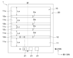
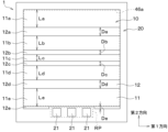
- the semiconductor device 1 has a cell region 10 and a peripheral region 20 surrounding the cell region 10.
- the cell region 10 has an IGBT region 11 in which an IGBT element is formed, and an FWD region 12 in which an FWD element is formed.
- the semiconductor device 1 of this embodiment is an RC (short for Reverse Conducting)-IGBT in which the IGBT region 11 and the FWD region 12 are formed in a common semiconductor substrate 30, which will be described later.
- the portion on the collector layer 41 located on the other surface 30b of the semiconductor substrate 30 is the IGBT region 11
- the portion on the cathode layer 42 located on the other surface 30b of the semiconductor substrate 30 is the FWD region 12.
- the cell region 10 has a generally rectangular shape in plan view.
- the IGBT region 11 and the FWD region 12 are formed to have portions that are alternately arranged along one direction within the cell region 10.
- the IGBT region 11 and the FWD region 12 are formed to have portions that are alternately arranged along one direction in the surface direction of the semiconductor substrate 30, which will be described later.
- the IGBT region 11 and the FWD region 12 are rectangular regions each having a longitudinal direction, and are alternately formed along a cross direction that crosses the longitudinal direction.
- the longitudinal direction of the IGBT region 11 and the FWD region 12 is referred to as a first direction
- the cross direction is referred to as a second direction.
- the left-right direction on the paper surface is the first direction
- the up-down direction on the paper surface is the second direction.
- the first direction can be said to be one direction in the surface direction of the semiconductor substrate 30 described later
- the second direction can be said to be a direction perpendicular to the first direction and along the surface direction of the semiconductor substrate 30 described later.
- the IGBT regions 11 and the FWD regions 12 in this embodiment are arranged alternately so that the IGBT regions 11 are located at both ends in the second direction.
- five IGBT regions 11 are formed along the second direction, and four FWD regions 12 are formed along the second direction.
- an odd number of IGBT regions 11 are formed, and an even number of FWD regions 12 are formed.
- the center of the cell region 10 in the second direction is the IGBT region 11.
- the five IGBT regions 11 arranged along the second direction are also referred to as the first IGBT region 11a, the second IGBT region 11b, the third IGBT region 11c, the fourth IGBT region 11d, and the fifth IGBT region 11e, in that order along the second direction.
- the four FWD regions 12 arranged along the second direction are also referred to as the first FWD region 12a, the second FWD region 12b, the third FWD region 12c, and the fourth FWD region 12d, in that order along the second direction.
- the third IGBT region 11c is located in the center of the cell region 10 in the second direction.
- the length along the second direction is also referred to as the width.
- the widths La to Le of the first to fifth IGBT regions 11a to 11e and the widths Da to Dd of the first to fourth FWD regions 12a to 12d are adjusted as follows.
- the width of the IGBT region 11 located on the central side in the second direction is narrower than the width of the region located on the end side in the second direction.
- the first to fifth IGBT regions 11a to 11e are formed such that the width Lc of the third IGBT region 11c is the narrowest, followed by the widths Lb and Ld of the second and fourth IGBT regions 11b and 11d, and the widths La and Le of the first and fifth IGBT regions 11a and 11e.
- the width Lb of the second IGBT region 11b and the width Ld of the fourth IGBT region 11d are made equal, and the width La of the first IGBT region 11a and the width Le of the fifth IGBT region 11e are made equal.
- the first to fourth FWD regions 12a to 12d are formed so that their widths Da to Dd are equal.
- a plurality of pad portions 21 are formed, which are connected to a gate electrode 35 (described later) and a temperature sensing element (not shown), etc.
- three pad portions 21 are arranged, and are arranged along the first direction in the portion of the peripheral region 20 on the side of the fifth IGBT region 11e.
- the semiconductor device 1 has a semiconductor substrate 30 that constitutes an N -type drift layer 31.
- the semiconductor substrate 30 is made of a silicon substrate.
- a P- type base layer 32 is formed on the drift layer 31.
- the base layer 32 is formed on one surface 30a of the semiconductor substrate 30.
- a plurality of trenches 33 are formed in the semiconductor substrate 30 so as to penetrate the base layer 32 from the one surface 30a side to reach the drift layer 31. As a result, the base layer 32 is separated into a plurality of pieces by the trenches 33.
- the plurality of trenches 33 are formed in the IGBT region 11 and the FWD region 12, respectively. Also, in this embodiment, the plurality of trenches 33 are formed in a stripe shape with the first direction as the longitudinal direction.
- the gate electrode 35 arranged in the trench 33 formed in the IGBT region 11 is connected to one of the pads 21 shown in FIG. 1 via a gate wiring (not shown), so that a predetermined gate voltage is applied.
- the gate electrode 35 arranged in the trench 33 formed in the FWD region 12 is electrically connected to an upper electrode 39, which will be described later. In other words, the gate electrode 35 in the FWD region 12 is maintained at a predetermined potential.
- An N + type emitter region 36 having a higher impurity concentration than the drift layer 31 is formed in a surface layer portion of the base layer 32 of the IGBT region 11 and the FWD region 12 (i.e., on the side of the one surface 30a of the semiconductor substrate 30).
- a P + type contact region 37 having a higher impurity concentration than the base layer 32 is formed in a surface layer portion of the base layer 32 of the IGBT region 11 and the FWD region 12.
- the emitter region 36 is formed to terminate in the base layer 32 and to contact the side surface of the trench 33.
- the contact region 37 is formed to terminate in the base layer 32, similar to the emitter region 36.
- the emitter region 36 is structured to extend in a rod shape in the region between the trenches 33 along the longitudinal direction of the trench 33 so as to contact the side of the trench 33, and to terminate inside the tip of the trench 33.
- the contact region 37 is sandwiched between the two emitter regions 36 and extends in a rod shape along the longitudinal direction of the trench 33 (i.e., the emitter regions 36).
- the portion of the wall surface of the trench 33 that is located between the emitter region 36 and the drift layer 31 becomes the surface of the base layer 32 that is located between the emitter region 36 and the drift layer 31.
- the contact region 37 in this embodiment is formed deeper than the emitter region 36 with respect to one surface 30a of the semiconductor substrate 30.
- An interlayer insulating film 38 made of BPSG (short for borophosphosilicate glass) or the like is formed on one surface 30a of the semiconductor substrate 30.
- An upper electrode 39 is formed on the interlayer insulating film 38 and is electrically connected to the emitter region 36 and the contact region 37 (i.e., the base layer 32) through a contact hole 38a formed in the interlayer insulating film 38.
- an upper electrode 39 is formed on the interlayer insulating film 38, which functions as an emitter electrode in the IGBT region 11 and functions as an anode electrode in the FWD region 12.
- a contact hole 38b that exposes the gate electrode 35 is formed in the interlayer insulating film 38 in the FWD region 12.
- the upper electrode 39 is also connected to the gate electrode 35 through this contact hole 38b.
- the gate electrode 35 formed in the FWD region 12 is maintained at the same potential as the upper electrode 39.
- An N-type field stop layer (hereinafter referred to as an FS layer) 40 having a higher impurity concentration than the drift layer 31 is formed on the side of the drift layer 31 opposite the base layer 32 side (i.e., the other surface 30b side of the semiconductor substrate 30).
- a P + type collector layer 41 is formed on the opposite side to the drift layer 31 with the FS layer 40 in between, and in the FWD region 12, an N + type cathode layer 42 is formed on the opposite side to the drift layer 31 with the FS layer 40 in between. That is, the IGBT region 11 and the FWD region 12 are separated from each other by whether the layer formed on the other surface 30b side of the semiconductor substrate 30 is the collector layer 41 or the cathode layer 42.
- the collector layer 41 is formed on the opposite side to the drift layer 31 with the FS layer 40 in between.
- a lower electrode 43 is formed on the opposite side of the collector layer 41 and the cathode layer 42 from the drift layer 31 (i.e., the other surface 30b of the semiconductor substrate 30).
- the lower electrode 43 is formed to function as a collector electrode in the IGBT region 11 and as a cathode electrode in the FWD region 12.
- the lower electrode 43 is also connected to the collector layer 41 in the peripheral region 20.
- a PN junction FWD element is formed with the base layer 32 and contact region 37 as the anode, and the drift layer 31, FS layer 40, and cathode layer 42 as the cathode.
- the peripheral region 20 has a drift layer 31 similar to that of the cell region 10.
- a P + type deep layer 44 is formed at the boundary with the cell region 10, connected to the base layer 32, and has a higher impurity concentration than the base layer 32 so that electric field concentration in the cell region 10 is suppressed.
- the deep layer 44 is formed deeper than the base layer 32 and is formed in a frame shape so as to surround the cell region 10.
- the parts located at the corners are formed in an R shape having a rounded curvature.
- the deep layer 44 is formed in a planar frame shape such as a square frame shape or a circular frame shape with rounded corners.
- a guard ring 45 is formed on the surface layer of the drift layer 31 so as to surround the deep layer 44.
- multiple guard rings 45 are formed, each having a ring structure surrounding the cell region 10.
- the guard rings 45 are formed to form a multiple ring structure.
- each guard ring 45 has a planar shape such as a square frame with rounded corners or a circular frame.
- the pad portion 21 arranged in the outer peripheral region 20 is arranged on the deep layer 44.
- an interlayer insulating film 38 is formed on one surface 30a of the semiconductor substrate 30.
- a contact hole 38c that exposes the deep layer 44 is formed in the interlayer insulating film 38, and the upper electrode 39 is also connected to the deep layer 44 through the contact hole 38c.
- a protective film 46 made of polyimide or the like is formed on one surface 30a of the semiconductor substrate 30.
- a contact hole 46a is formed in the protective film 46 to expose the upper electrode 39 in the cell region 10, and a contact hole 46b is formed to expose the pad portion 21 in the peripheral region 20.
- the contact hole 46a is formed to expose the entire cell region 10, and the opening is formed to be approximately rectangular in plan view to match the cell region 10.
- the N type, N + type, and N - type correspond to the first conductivity type
- the P type and P + type correspond to the second conductivity type
- the semiconductor device 1 is configured as described above, so that the semiconductor substrate 30 includes the collector layer 41, the cathode layer 42, the drift layer 31, the base layer 32, the emitter region 36, the contact region 37, etc.
- the PN junction formed between the base layer 32 and the drift layer 31 becomes reverse conductive, forming a depletion layer.
- a low-level gate voltage e.g., 0 V
- a high-level gate voltage equal to or higher than the threshold voltage Vth of the insulated gate structure is applied to the gate electrode 35 of the IGBT region 11 while a voltage higher than that of the upper electrode 39 is applied to the lower electrode 43.
- Vth threshold voltage
- an inversion layer is formed in the portion of the base layer 32 that contacts the trench 33 in which the gate electrode 35 is disposed.
- electrons are supplied to the drift layer 31 from the emitter region 36 via the inversion layer, and holes are supplied to the drift layer 31 from the collector layer 41, and the resistance value of the drift layer 31 is reduced by conductivity modulation.
- a current flows between the upper electrode 39 and the lower electrode 43 in the IGBT element.
- the width of the IGBT region 11 located on the central side in the second direction is narrower than the width of the region located on the end side in the second direction.
- the region of the IGBT region 11 located on the central side in the second direction has a smaller amount of current and generates less heat than the region located on the end side in the second direction.
- the IGBT region 11 is more difficult to dissipate heat in the part located on the central side in the second direction that dissipates heat more easily than the part located on the end side in the second direction that dissipates heat more easily. Therefore, when the IGBT element is in the on state, it is possible to prevent the region on the central side in the second direction of the cell region 10 from becoming too hot.
- FIG. 3 a semiconductor device in which the widths La to Le of the first to fifth IGBT regions 11a to 11e are equal is taken as the semiconductor device J1 of the comparative example.
- the temperatures of the semiconductor device 1 of this embodiment and the semiconductor device J1 of the comparative example are as shown in FIG. 4.
- the temperatures in FIG. 4 indicate the temperatures of the portions along the lines IV-IV in FIG. 1 and FIG. 3.
- 11a to 11e in FIG. 4 indicate the centers in the second direction of the first to fifth IGBT regions 11a to 11e, respectively.
- the widths La to Le of the first to fifth IGBT regions 11a to 11e are equal, so it is confirmed that the temperature is higher toward the center in the second direction. More specifically, the temperature of the third IGBT region 11c becomes extremely high.
- the width of the portion located toward the center in the second direction is narrower than the width of the portion located toward the end in the second direction.
- the width Lc of the third IGBT region 11c is narrower than the first, second, fourth, and fifth IGBT regions 11a, 11b, 11d, and 11e. This makes it possible to prevent the temperature of the third IGBT region 11c, which is the most difficult to dissipate heat, from becoming too high.
- the widths La to Le of the first to fifth IGBT regions 11a to 11e are adjusted so that the average temperatures of the first to fifth IGBT regions 11a to 11e are approximately equal.
- the semiconductor device 1 has greater heat dissipation properties toward the ends in the second direction.
- the first to fifth IGBT regions 11a to 11e of this embodiment are formed so that the width Lc of the third IGBT region 11c is the narrowest, and the widths Lb and Ld of the second and fourth IGBT regions 11b and 11d, and the widths La and Le of the first and fifth IGBT regions 11a and 11e become wider in this order. This makes it possible to suppress variations in the life span, etc. of the gate insulating film 34 in the first to fifth IGBT regions 11a to 11e.
- FIG. 5 shows the results when the widths La, Lb, Ld, and Le of the first, second, fourth, and fifth IGBT regions 11a, 11b, 11d, and 11e are equal while the width Lc of the third IGBT region 11c is narrowest as shown in FIG. 6.
- the maximum temperature of the semiconductor device 1 in FIG. 5 is the temperature of the third IGBT region 11c when the IGBT element is in the on state.
- the maximum temperature of the semiconductor device 1 drops sharply as the IGBT region width ratio increases when the ratio of the maximum width of the IGBT region 11 to the minimum width of the IGBT region 11 (hereinafter simply referred to as the IGBT region width ratio) is in the range of less than 1.5.
- the maximum temperature of the semiconductor device 1 hardly changes when the IGBT region width ratio is in the range of 1.5 to 4.5. Therefore, it is preferable that the IGBT region width ratio is in the range of 1.5 to 4.5. This makes it possible to sufficiently lower the temperature of the third IGBT region 11c.
- the IGBT element when the IGBT element is turned off and the FWD element is turned on (i.e., the FWD element operates as a diode), the voltages applied to the upper electrode 39 and the lower electrode 43 are switched, and a forward voltage is applied to the upper electrode 39, where a voltage higher than that of the lower electrode 43 is applied.
- holes are supplied to the base layer 32 and electrons are supplied to the cathode layer 42, causing the FWD element to operate as a diode.
- the semiconductor device 1 described above is used, for example, to configure a semiconductor module for driving a motor as a load.
- the semiconductor module is configured to include a first support member 110, a semiconductor device 1, a terminal 120, a second support member 130, a control terminal portion 140, a sealing member 160, etc.
- the first support member 110 is composed of a lead frame made of, for example, copper, iron, or an alloy thereof.
- the first support member 110 has a first mounting portion 111 having a surface 111a and a back surface 111b opposite the surface 111a, and a first connection terminal portion 112 connected to the first mounting portion 111.
- the first connection terminal portion 112 extends along the surface direction of the surface 111a of the first mounting portion 111, and is integrated with the first mounting portion 111 in this embodiment. In this embodiment, the first connection terminal portion 112 extends opposite the control terminal portion 140, which will be described later.
- the semiconductor device 1 is configured as described above, and is disposed on the surface 111a of the first mounting portion 111 via a first joining member 201 made of solder or the like, with the lower electrode 43 facing the first mounting portion 111.
- the terminal 120 is made of, for example, copper, iron, or an alloy thereof, and has a shape corresponding to the planar shape of the upper electrode 39 exposed from the protective film 46 in the semiconductor device 1.
- the opening of the contact hole 46a formed in the protective film 46 is approximately rectangular, so the terminal 120 has an approximately rectangular planar shape.
- the terminal 120 is then placed on the upper electrode 39 of the semiconductor device 1 via a second joining member 202 made of solder or the like.
- a plating layer is formed on the portion of the protective film 46 exposed from the contact hole 46a in order to improve wettability with the solder that constitutes the second bonding member 202.
- the terminal 120 is then placed on this plating layer via the second bonding member 202.
- the second support member 130 is composed of a lead frame or the like similar to the first support member 110, and has a second mounting portion 131 having a surface 131a and a back surface 131b opposite the surface 131a, and a second connection terminal portion 132 connected to the second mounting portion 131.
- the second support member 130 has a surface 131a of the second mounting portion 131 connected to the terminal 120 via a third joining member 203 made of solder or the like. That is, the first support member 110 and the second support member 130 are arranged to face each other with the semiconductor device 1 in between.
- the second connection terminal portion 132 extends along the planar direction of the surface 131a of the second mounting portion 131, and in this embodiment, extends in the same direction as the first connection terminal portion 112. In this embodiment, the second connection terminal portion 132 is integrated with the second mounting portion 131.
- the control terminal section 140 is connected to the pad section 21 formed on the semiconductor device 1 via a bonding wire 150.
- the control terminal section 140 corresponds to the external terminal section.
- the sealing member 160 is made of molding resin, potting resin, or the like, and is formed to seal the first support member 110, the semiconductor device 1, the second support member 130, the control terminal portion 140, and the like. Specifically, the sealing member 160 is formed so that the back surface 111b of the first mounting portion 111 in the first support member 110, the back surface 131b of the second mounting portion 131 in the second support member 130, and a portion of each of the terminal portions 112, 132, and 140 are exposed.
- the width of the IGBT region 11 located in the center in the second direction is narrower than the width of the regions located on the end sides in the second direction. Therefore, compared to a case in which the widths of the IGBT regions 11 are equal, it is possible to prevent the temperature of the IGBT region 11 in the center in the second direction from becoming too high compared to the temperature of the IGBT region 11 on the end sides in the second direction. Therefore, for example, compared to the semiconductor device J1 of the comparative example, it is possible to increase the amount of current that can be passed before the maximum temperature becomes the same, thereby increasing the selectivity of applications.
- the width Lc of the third IGBT region 11c located in the center in the second direction is the narrowest. This makes it possible to prevent the temperature of the IGBT region 11 located in the center in the second direction from becoming too high. Note that, in this configuration, if X IGBT regions 11 are arranged along the second direction, where X is an odd number of 3 or more, then it can also be said that the width of the region located at the ⁇ (X+1)/2 ⁇ th position along the second direction is the narrowest.
- the maximum temperature of the semiconductor device 1 can be sufficiently reduced by setting the IGBT region width ratio to 1.5 to 4.5.
- the number and arrangement of the IGBT regions 11 and the FWD regions 12 can be appropriately changed.
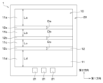
- four IGBT regions 11, ie, first to fourth IGBT regions 11a to 11d may be formed along the second direction, and three FWD regions 12, ie, first to third FWD regions 12a to 12c, may be formed. That is, in this example, an even number of IGBT regions 11 are formed, and an odd number of FWD regions 12 are formed.
- the FWD region 12 is arranged in the center of the cell region 10 in the second direction.
- the width of the IGBT region 11 at the center in the second direction is narrower than the width of the end in the second direction.
- the first to fourth IGBT regions 11a to 11d are formed such that the widths Lb and Lc of the second and third IGBT regions 11b and 11c are narrower than the widths La and Ld of the first and fourth IGBT regions 11a and 11d.
- the first embodiment can also be applied to the case where the number of IGBT regions 11 along the second direction is an even number of 4 or more.
- the semiconductor device 1 may have the IGBT region 11 and the FWD region 12 divided in the first direction as shown in FIG. 9.
- a gate liner connected to the gate electrode 35 may be disposed in the divided portion, or a temperature sensor may be disposed.
- the semiconductor device 1 may be configured such that the IGBT region 11 and the FWD region 12 extend in the second direction as the longitudinal direction and are arranged alternately along the first direction.
- the first direction corresponds to one direction along the surface direction of the semiconductor substrate 30.
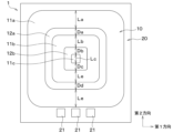
- the semiconductor device 1 may have the IGBT regions 11 and the FWD regions 12 formed alternately in a concentric frame shape, as shown in Figures 11 and 12.
- the first direction and the second direction are set as in the first embodiment, it can be said that the IGBT regions 11 and the FWD regions 12 are formed alternately along the first direction and the second direction.
- three IGBT regions 11, the first to third IGBT regions 11a to 11c, and two FWD regions 12, the first and second FWD regions 12a and 12b, are formed in a concentric frame shape.
- five IGBT regions 11 i.e., an odd number
- first and second IGBT regions 11a and 11b and two FWD regions 12, the first and second FWD regions 12a and 12b are formed in a concentric frame shape.
- four IGBT regions 11 i.e., an even number
- Second Embodiment A second embodiment will be described. This embodiment is different from the first embodiment in that the width of the FWD region 12 is changed. As the rest is the same as the first embodiment, the description will be omitted here.
- the temperature of the semiconductor device 1 is highest when the IGBT element is on, and therefore a configuration for changing the width of the IGBT region 11 has been described.
- the temperature of the semiconductor device 1 is highest when the FWD element is on. In this embodiment, an example will be described in which the temperature of the semiconductor device 1 is highest when the FWD element is on.
- the first to fifth IGBT regions 11a to 11e have the same widths La to Le.
- the first to fifth FWD regions 12a to 12d have a narrower width at the center in the second direction than at the ends in the second direction.
- the widths Db and Dc of the second and third FWD regions 12b and 12c are narrower than the widths Da and Dd of the first and fourth FWD regions 12a and 12d.
- the inventors also investigated the maximum temperature of the semiconductor device 1 with the FWD element in the on state, and, although not shown, obtained results similar to those in FIG. 5. That is, it was confirmed that the maximum temperature of the semiconductor device 1 drops more steeply as the FWD region width ratio increases when the ratio of the maximum width of the FWD region 12 to the minimum width of the FWD region 12 (hereinafter simply referred to as the FWD region width ratio) is in the range of less than 1.5. It was also confirmed that the maximum temperature of the semiconductor device 1 hardly changes when the FWD region width ratio is in the range of 1.5 to 4.5. Therefore, it is preferable that the FWD region width ratio is in the range of 1.5 to 4.5.
- the maximum temperature in the semiconductor device 1 of this embodiment is the temperature of the second and third FWD regions 12b and 12c.
- the width of the region of the FWD region 12 located at the center in the second direction is narrower than the width of the region located at the end side in the second direction. Therefore, compared to a case where the widths of the FWD regions 12 are equal, it is possible to prevent the temperature of the FWD region 12 at the center in the second direction from becoming too high compared to the temperature of the FWD region 12 at the end side in the second direction.
- the widths Db, Dc of the second and third FWD regions 12b, 12c located in the center in the second direction are narrowest. This makes it possible to prevent the temperature of the FWD region 12 located in the center in the second direction from becoming too high. Note that, in this configuration, if X number of FWD regions 12, where X is an even number equal to or greater than four, are arranged along the second direction, it can also be said that the widths of the (X/2)th region and the ⁇ (X/2)+1 ⁇ th region along the second direction are narrowest.
- the maximum temperature of the semiconductor device 1 can be sufficiently reduced by setting the FWD region width ratio to 1.5 to 4.5.
- an odd number of FWD regions 12 may be arranged along the second direction.
- the width of the region located at the ⁇ (X+1)/2 ⁇ th position along the second direction should be the narrowest.
- Third Embodiment A third embodiment will be described. This embodiment is a combination of the first and second embodiments. As the rest of the third embodiment is similar to the first embodiment, a description thereof will be omitted here.
- the semiconductor device 1 of this embodiment is configured by combining the first and second embodiments.
- the first to fifth IGBT regions 11a to 11e are formed such that the width Lc of the third IGBT region 11c is the narrowest, followed by the widths Lb and Ld of the second and fourth IGBT regions 11b and 11d, and the widths La and Le of the first and fifth IGBT regions 11a and 11e.
- the first to fourth FWD regions 12a to 12d are formed such that the widths Db and Dc of the second and third FWD regions 12b and 12c are narrower than the widths Da and Dd of the first and fourth FWD regions 12a and 12d.
- the semiconductor device 1 of this embodiment has the first to fifth IGBT regions 11a to 11e and the first to fourth FWD regions 12a to 12d, similar to the first embodiment.
- the pad portion 21 is arranged in the outer peripheral region 20 on the opposite side of the fifth IGBT region 11e from the fourth FWD region 12d. In other words, the pad portion 21 is arranged in the vicinity of the fifth IGBT region 11e.
- both the first IGBT region 11a and the fifth IGBT region 11e tend to dissipate heat to the outer periphery region 20, and therefore the heat dissipation is likely to be high.
- the pad portion 21 of the outer periphery region 20 is disposed in the vicinity of the fifth IGBT region 11e, the portion of the outer periphery region 20 located on the fifth IGBT region 11e side is configured to be wider than the portion located on the first IGBT region 11a side. Therefore, when comparing the first IGBT region 11a and the fifth IGBT region 11e, the fifth IGBT region 11e has higher heat dissipation properties than the first IGBT region 11a.
- the width Le of the fifth IGBT region 11e is made wider than the width La of the first IGBT region 11a.
- the width La of the first IGBT region 11a is made wider than the widths Lb to Ld of the second to fourth IGBT regions 11b to 11d.
- the width of the IGBT region 11 located at the center in the second direction is narrower than the width of the region located at the end in the second direction. Therefore, the same effect as the first embodiment can be obtained.
- the width Le of the fifth IGBT region 11e located on the pad portion 21 side of the IGBT region 11 is wider than the width La of the first IGBT region 11a. This makes it possible to prevent the temperature of the first IGBT region 11a, which has lower heat dissipation properties than the fifth IGBT region 11e, from becoming higher than the temperature of the fifth IGBT region 11e.
- the semiconductor device 1 of this embodiment has the first to fifth IGBT regions 11a to 11e and the first to fourth FWD regions 12a to 12d, similar to the second embodiment.
- the pad portion 21 is disposed on the fourth FWD region 12d side.
- the fourth FWD region 12d has higher heat dissipation properties than the first FWD region 12a.
- the width Dd of the fourth FWD region 12d is made wider than the width Da of the first FWD region 12a.
- the width Da of the first FWD region 12a is made wider than the widths Db and Dc of the second and third FWD regions 12b and 12c.
- the width of the region located at the center in the second direction of the FWD region 12 is narrower than the width of the region located at the end in the second direction. Therefore, it is possible to obtain the same effect as the second embodiment described above.
- the width Dd of the fourth FWD region 12d located on the pad portion 21 side of the FWD region 12 is made wider than the width Da of the first FWD region 12a. This makes it possible to prevent the temperature of the first FWD region 12a, which has lower heat dissipation properties than the fourth FWD region 12d, from becoming higher than the temperature of the fourth FWD region 12d.
- the FWD region 12 has a fifth FWD region 12e that is disposed on the opposite side of the fifth IGBT region 11e from the fourth FWD region 12d.
- the fifth FWD region 12e is disposed adjacent to the pad portion 21 in the first direction.
- two fifth FWD regions 12e are provided, each having a rectangular shape in plan view, and are formed to sandwich the pad portion 21 in the first direction.
- the fifth FWD region 12e is divided in the first direction, and the pad portion 21 is arranged in the portion where the fifth FWD region 12e is divided.
- the region adjacent to the pad portion 21 in the second direction is the IGBT region 11
- the region adjacent to the pad portion 21 in the first direction is the FWD region 12.
- the arrangement region RP in the cell region 10 the region adjacent to the arrangement region RP in the second direction is the IGBT region 11, and the region adjacent to the arrangement region RP in the first direction is the FWD region 12.
- the fifth FWD region 12e corresponds to the additional FWD region.
- the contact hole 46a formed in the protective film 46 has an opening shape that is generally rectangular in plan view, similar to the first embodiment.
- the contact hole 46a formed in the protective film 46 is formed so as to expose the first to fifth IGBT regions 11a to 11e and the first to fourth FWD regions 12a to 12d, and is formed so as to cover the fifth FWD region 12e.
- the opening of the contact hole 46a is formed so as to also expose the fifth FWD region 12e. That is, it becomes easier to control the spread of the second bonding member 202 (i.e., solder) when constructing a semiconductor module. This makes it possible to suppress variations in the bonding strength between the terminal 120 and the semiconductor device 1 and in the heat dissipation properties to the terminal 120.
- the second bonding member 202 i.e., solder
- the fifth FWD region 12e is covered by the protective film 46, and therefore tends to have lower heat dissipation properties compared to the first to fourth FWD regions 12a to 12d exposed through the contact holes 46a in the protective film 46. Therefore, in this embodiment, the width De of the fifth FWD region 12e is narrower than the widths Da to Dd of the first to fourth FWD regions 12a to 12d.
- the width of the region located at the center in the second direction in the region exposed through the contact hole 46a is narrower than the width of the region located at the end side in the second direction.
- the widths of the IGBT region 11 and the FWD region 12 are the same as those of the third embodiment, and therefore the same effects as those of the third embodiment can be obtained.
- the fifth FWD region 12e is disposed in a position adjacent to the pad portion 21 in the first direction. Therefore, since the FWD region 12 is disposed in the region that was the outer periphery region 20 in the first embodiment, the thermal resistance of the FWD region 12 can be reduced.
- a deep layer 44 is formed in the outer peripheral region 20, surrounding the cell region 10 and connected to the base layer 32. Therefore, when the FWD element is turned on, holes can also be supplied from the deep layer 44. In this case, if the FWD region 12 is arranged in a position adjacent to the pad portion 21 in the second direction, the amount of holes supplied when the FWD element is in the on state may be too large, resulting in a decrease in the recovery tolerance. Therefore, in this embodiment, the IGBT region 11 is arranged in a position adjacent to the pad portion 21 in the second direction. This makes it possible to increase the active area of the FWD region 12 while suppressing a decrease in the recovery tolerance.
- the width De of the fifth FWD region 12e is narrower than the widths Da to Dd of the first to fourth FWD regions 12a to 12d. This makes it possible to prevent the temperature of the fifth FWD region 12e, which is covered with the protective film 46, from increasing.
- the pad portion 21 may be disposed on one end side of the cell region 10 in the first direction so as to be adjacent to the fifth IGBT region 11e in the second direction.
- the configuration in which the fifth FWD region 12e is arranged can also be applied to a configuration in which the IGBT region 11 and the FWD region 12 are arranged in a concentric frame shape.
- the contact hole 46a formed in the protective film 46 may be formed so as to expose the fifth FWD region 12e.
- the width De of the fifth FWD region 12e may be made wider than the width Da of the first FWD region 12a.
- the FWD region 12 may be disposed adjacent to the pad portion 21 in the second direction.
- Seventh Embodiment A seventh embodiment will be described. This embodiment is different from the sixth embodiment in that the shape of the fifth FWD region 12e is changed. As the rest is the same as the sixth embodiment, the description will be omitted here.
- the deep layer 44 is formed into a planar frame shape such as a square or circle with rounded corners.
- the end of the fifth FWD region 12e opposite the pad section 21 side will have a close portion and a far portion in terms of the distance between the cathode layer 42 and the deep layer 44, and the electric field will be more likely to concentrate in the portion where the distance between the cathode layer 42 and the deep layer 44 is closer.
- the fifth FWD region 12e of this embodiment has an end C in the first direction opposite the pad section 21 side, which is formed into a planar shape that is rounded to correspond to the shape of the deep layer 44. This configuration is realized by adjusting the planar shape of the cathode layer 42.
- the widths of the IGBT region 11 and the FWD region 12 are the same as those of the third embodiment, and therefore the same effects as those of the third embodiment can be obtained.
- the fifth FWD region 12e is an end in the first direction, and the end C on the opposite side to the pad portion 21 has a rounded planar shape so as to correspond to a corner of the deep layer 44. This reduces the variation in the distance between the cathode layer 42 and the deep layer 44, making it difficult for electric field concentration to occur.
- the first conductivity type was N-type and the second conductivity type was P-type, but the first conductivity type could also be P-type and the second conductivity type could also be N-type.
- the semiconductor device 1 may be a planar type in which the gate electrode 35 is disposed on one surface 30a of the semiconductor substrate 30, rather than a trench gate type.
- the gate electrode 35 of the FWD region 12 does not have to be connected to the upper electrode 39. Also, in each of the above embodiments, the FWD region 12 does not have to have a trench gate structure, and the emitter region 36 does not have to be formed.
- the second embodiment can be combined as appropriate so that the width of the FWD region 12 located at the center in the second direction is narrower than the width of the region located at the end in the second direction.
- the widths of the IGBT regions 11 can be made equal to each other.
- the fourth embodiment can also be combined as appropriate so that the width Le of the fifth IGBT region 11e located on the pad portion 21 side is narrower than the width La of the first IGBT region 11a.
- the fifth embodiment can also be combined as appropriate so that the width Dd of the fourth FWD region 12d located on the pad portion 21 side is narrower than the width Da of the first FWD region 12a.
- a semiconductor device comprising: A semiconductor substrate (30) having a cell region (10) and an outer peripheral region (20) surrounding the cell region; an IGBT region (11) formed in the cell region and having an IGBT element; an FWD region (12) formed in the cell region and having an FWD element; the IGBT region and the FWD region are alternately formed in one direction in a surface direction of the semiconductor substrate,
- the semiconductor device has three or more IGBT regions formed in the one direction, and when the length along the one direction is defined as the width, the width of the region located toward the center in the one direction is narrower than the width of the region located toward the end in the one direction.
- the number of the IGBT regions along the one direction is X, which is an odd number equal to or greater than 3; 2.
- the IGBT region has a width that is narrowest at a region located at an ⁇ (X+1)/2 ⁇ th position along the one direction.
- the number of the IGBT regions along the one direction is X, which is an even number equal to or greater than 4;
- the semiconductor device according to the first aspect wherein the IGBT region has an equal width to a region located at an (X/2)th position along the one direction and a region located at an ⁇ (X/2)+1 ⁇ th position along the one direction, and the widths of the IGBT region are narrowest.
- the peripheral region has a pad portion (21) connected to an external terminal portion (140), 3.
- a semiconductor device comprising: A semiconductor substrate (30) having a cell region (10) and an outer peripheral region (20) surrounding the cell region; an IGBT region (11) formed in the cell region and having an IGBT element; an FWD region (12) formed in the cell region and having an FWD element; the IGBT region and the FWD region are alternately formed in one direction in a surface direction of the semiconductor substrate,
- the semiconductor device has three or more FWD regions formed in the one direction, and when the length along the one direction is taken as the width, the width of a region located on the central side in the one direction is narrower than the width of a region located on the end side in the one direction.
- the number of the FWD regions along the one direction is X, which is an odd number equal to or greater than 3;
- the number of the FWD regions along the one direction is X, which is an even number equal to or greater than 4;
- the peripheral region has a pad portion (21) connected to an external terminal portion (140),
- the semiconductor device according to any one of the sixth to ninth aspects, wherein the width of the FWD region is closest to the pad portion side and is wider than the width of the region farthest from the pad portion side.
- the peripheral region has a pad portion (21) connected to an external terminal portion (140), the FWD region has an additional FWD region (12e) adjacent to the pad portion in a cross direction crossing the one direction,
- the semiconductor device according to any one of the sixth to eleventh aspects, wherein the IGBT region is disposed at a position adjacent to the pad portion in one direction.
- the semiconductor substrate is the transistor has a drift layer (31) of a first conductivity type, a base layer (32) of a second conductivity type formed in a surface portion of the drift layer in the cell region, an emitter region (36) of the first conductivity type formed in a surface portion of the base layer away from the drift layer in the IGBT region and having a higher impurity concentration than the drift layer, a collector layer (41) of the second conductivity type formed on a side of the drift layer opposite to the base layer side in the IGBT region, and a cathode layer (42) of the first conductivity type formed on a side of the drift layer opposite to the base layer side in the FWD region, A deep layer (44) of a second conductivity type is formed in the outer peripheral region at the boundary with the cell region, the deep layer (44) being connected to the base layer and surrounding the cell region; The deep layer is in the shape of a flat frame with rounded corners,
- the semiconductor device according to the twelfth or thirteenth aspect, wherein the
Landscapes
- Metal-Oxide And Bipolar Metal-Oxide Semiconductor Integrated Circuits (AREA)
Priority Applications (1)
| Application Number | Priority Date | Filing Date | Title |
|---|---|---|---|
| CN202480051834.7A CN121713664A (zh) | 2023-08-09 | 2024-08-02 | 半导体装置 |
Applications Claiming Priority (2)
| Application Number | Priority Date | Filing Date | Title |
|---|---|---|---|
| JP2023-130237 | 2023-08-09 | ||
| JP2023130237A JP2025025459A (ja) | 2023-08-09 | 2023-08-09 | 半導体装置 |
Publications (1)
| Publication Number | Publication Date |
|---|---|
| WO2025033354A1 true WO2025033354A1 (ja) | 2025-02-13 |
Family
ID=94534834
Family Applications (1)
| Application Number | Title | Priority Date | Filing Date |
|---|---|---|---|
| PCT/JP2024/027756 Pending WO2025033354A1 (ja) | 2023-08-09 | 2024-08-02 | 半導体装置 |
Country Status (3)
| Country | Link |
|---|---|
| JP (1) | JP2025025459A (https=) |
| CN (1) | CN121713664A (https=) |
| WO (1) | WO2025033354A1 (https=) |
Citations (4)
| Publication number | Priority date | Publication date | Assignee | Title |
|---|---|---|---|---|
| JP2011134950A (ja) * | 2009-12-25 | 2011-07-07 | Toyota Motor Corp | 半導体装置 |
| JP2021028930A (ja) * | 2019-08-09 | 2021-02-25 | 富士電機株式会社 | 半導体装置 |
| JP2021190657A (ja) * | 2020-06-04 | 2021-12-13 | 三菱電機株式会社 | 半導体装置 |
| JP2023161772A (ja) * | 2022-04-26 | 2023-11-08 | 三菱電機株式会社 | 半導体装置および電力変換装置 |
-
2023
- 2023-08-09 JP JP2023130237A patent/JP2025025459A/ja active Pending
-
2024
- 2024-08-02 WO PCT/JP2024/027756 patent/WO2025033354A1/ja active Pending
- 2024-08-02 CN CN202480051834.7A patent/CN121713664A/zh active Pending
Patent Citations (4)
| Publication number | Priority date | Publication date | Assignee | Title |
|---|---|---|---|---|
| JP2011134950A (ja) * | 2009-12-25 | 2011-07-07 | Toyota Motor Corp | 半導体装置 |
| JP2021028930A (ja) * | 2019-08-09 | 2021-02-25 | 富士電機株式会社 | 半導体装置 |
| JP2021190657A (ja) * | 2020-06-04 | 2021-12-13 | 三菱電機株式会社 | 半導体装置 |
| JP2023161772A (ja) * | 2022-04-26 | 2023-11-08 | 三菱電機株式会社 | 半導体装置および電力変換装置 |
Also Published As
| Publication number | Publication date |
|---|---|
| JP2025025459A (ja) | 2025-02-21 |
| CN121713664A (zh) | 2026-03-20 |
Similar Documents
| Publication | Publication Date | Title |
|---|---|---|
| JP5232367B2 (ja) | 半導体装置 | |
| US10177134B2 (en) | Semiconductor device | |
| JP7494953B2 (ja) | 半導体モジュール | |
| US10256212B2 (en) | Semiconductor chip having multiple pads and semiconductor module including the same | |
| JP7301124B2 (ja) | 半導体装置 | |
| JP7635685B2 (ja) | 半導体装置および電力変換装置 | |
| JP2023024670A (ja) | 半導体装置 | |
| JP7722535B2 (ja) | 半導体モジュール | |
| WO2014045842A1 (ja) | 半導体装置 | |
| CN110140220B (zh) | 半导体装置 | |
| JP7256771B2 (ja) | 半導体装置 | |
| US10741550B2 (en) | Reverse-conducting insulated gate bipolar transistor | |
| WO2022219930A1 (ja) | 半導体装置および半導体モジュール | |
| CN112054019B (zh) | 半导体装置 | |
| WO2025033354A1 (ja) | 半導体装置 | |
| JP2021040062A (ja) | 半導体装置 | |
| US11799023B2 (en) | Semiconductor device | |
| JP2022178755A (ja) | 半導体モジュール | |
| JP7746241B2 (ja) | 半導体モジュール | |
| WO2025100377A1 (ja) | 半導体装置 | |
| JP2009141067A (ja) | 半導体装置 | |
| CN114256326B (zh) | 半导体装置 | |
| WO2024185848A1 (ja) | 半導体装置 | |
| WO2024224669A1 (ja) | パワーモジュール | |
| WO2024135114A1 (ja) | 半導体装置および半導体モジュール |
Legal Events
| Date | Code | Title | Description |
|---|---|---|---|
| NENP | Non-entry into the national phase |
Ref country code: DE |