WO2025033099A1 - 半導体装置 - Google Patents
半導体装置 Download PDFInfo
- Publication number
- WO2025033099A1 WO2025033099A1 PCT/JP2024/025288 JP2024025288W WO2025033099A1 WO 2025033099 A1 WO2025033099 A1 WO 2025033099A1 JP 2024025288 W JP2024025288 W JP 2024025288W WO 2025033099 A1 WO2025033099 A1 WO 2025033099A1
- Authority
- WO
- WIPO (PCT)
- Prior art keywords
- semiconductor device
- main portion
- sealing resin
- section
- main
- Prior art date
- Legal status (The legal status is an assumption and is not a legal conclusion. Google has not performed a legal analysis and makes no representation as to the accuracy of the status listed.)
- Pending
Links
Images


Classifications
-
- H—ELECTRICITY
- H10—SEMICONDUCTOR DEVICES; ELECTRIC SOLID-STATE DEVICES NOT OTHERWISE PROVIDED FOR
- H10W—GENERIC PACKAGES, INTERCONNECTIONS, CONNECTORS OR OTHER CONSTRUCTIONAL DETAILS OF DEVICES COVERED BY CLASS H10
- H10W72/00—Interconnections or connectors in packages
-
- H—ELECTRICITY
- H10—SEMICONDUCTOR DEVICES; ELECTRIC SOLID-STATE DEVICES NOT OTHERWISE PROVIDED FOR
- H10W—GENERIC PACKAGES, INTERCONNECTIONS, CONNECTORS OR OTHER CONSTRUCTIONAL DETAILS OF DEVICES COVERED BY CLASS H10
- H10W72/00—Interconnections or connectors in packages
- H10W72/071—Connecting or disconnecting
Definitions
- This disclosure relates to a semiconductor device.
- the semiconductor device disclosed in Patent Document 1 comprises a semiconductor element provided with an electrode pad, a first lead, a bonding wire conductively joined to the electrode pad and the first lead, and a sealing resin that covers the semiconductor element and the bonding wire. As a result, the first lead is electrically connected to the semiconductor element.
- An object of the present disclosure is to provide an improved semiconductor device compared to conventional semiconductor devices.
- an object of the present disclosure is to provide a semiconductor device capable of suppressing corrosion of electrodes of a semiconductor element caused by moisture that penetrates from the outside through a conductive member.
- the semiconductor device provided by the first aspect of the present disclosure comprises a semiconductor element having an electrode located on one side in a first direction, a conductive member conductively joined to the electrode, and a sealing resin covering the semiconductor element and the conductive member.
- the conductive member has a first joint portion conductively joined to the electrode and a main portion extending from the first joint portion. The dimension of the first joint portion in a direction perpendicular to the first direction is greater than the dimension of the main portion in a direction perpendicular to the direction in which the main portion extends.
- the sealing resin has a top surface facing the one side in the first direction.
- the main portion has a first portion located closest to the top surface in the first direction. When viewed in the first direction, the first portion is distant from the semiconductor element.
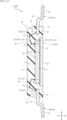
- FIG. 1 is a perspective view of a semiconductor device according to a first embodiment of the present disclosure.
- FIG. 2 is a plan view of the semiconductor device shown in FIG.
- FIG. 3 is a plan view corresponding to FIG. 2, and shows the sealing resin through the plan view.
- FIG. 4 is a bottom view of the semiconductor device shown in FIG.
- FIG. 5 is a bottom view corresponding to FIG. 4, showing the sealing resin through the view.
- FIG. 6 is a front view of the semiconductor device shown in FIG. 7 is a right side view of the semiconductor device shown in FIG.
- FIG. 8 is a left side view of the semiconductor device shown in FIG.
- FIG. 9 is a cross-sectional view taken along line IX-IX in FIG.
- FIG. 10 is a cross-sectional view taken along line XX in FIG.
- FIG. 11 is a cross-sectional view taken along line XI-XI of FIG.
- FIG. 12 is a partially enlarged view of FIG.
- FIG. 13 is a partially enlarged view of FIG.
- FIG. 14 is a partially enlarged view of FIG.
- FIG. 15 is a partially enlarged cross-sectional view of a semiconductor device according to a modified example of the first embodiment of the present disclosure.
- FIG. 16 is a plan view of the semiconductor device according to the second embodiment of the present disclosure, showing the semiconductor device through a sealing resin.
- FIG. 17 is a cross-sectional view taken along line XVII-XVII in FIG.
- FIG. 18 is a partially enlarged view of FIG. FIG.
- FIG. 19 is a plan view of the semiconductor device according to the third embodiment of the present disclosure, showing the semiconductor device through a sealing resin.
- FIG. 20 is a cross-sectional view taken along line XX-XX in FIG.
- FIG. 21 is a partially enlarged view of FIG.
- FIG. 22 is a plan view of the semiconductor device according to the fourth embodiment of the present disclosure, showing the semiconductor device through a sealing resin.
- FIG. 23 is a cross-sectional view taken along line XXIII-XXIII in FIG.
- FIG. 24 is a partially enlarged view of FIG.
- FIG. 25 is a cross-sectional view of a semiconductor device according to a fifth embodiment of the present disclosure.
- a semiconductor device A10 according to a first embodiment of the present disclosure will be described with reference to Figures 1 to 14.
- the semiconductor device A10 includes a semiconductor element 10, a first lead 20, a plurality of second leads 30, a plurality of conductive members 40, and a sealing resin 50.
- the package format of the semiconductor device A10 is a small outline package (SOP).
- SOP small outline package
- Figures 3 and 5 show the sealing resin 50 in a see-through manner for ease of understanding.
- the outline of the sealing resin 50 is shown by an imaginary line (double-dashed line).
- the normal direction of the mounting surface 211 of the pad portion 21 described later is called the "first direction z”.
- One direction perpendicular to the first direction z is called the "second direction x”.
- a direction perpendicular to both the first direction z and the second direction x is called the "third direction y”.
- the sealing resin 50 covers the semiconductor element 10, a portion of the first lead 20, a portion of each of the multiple second leads 30, and the multiple conductive members 40.
- the sealing resin 50 is an insulator.
- the sealing resin 50 is made of a material that contains, for example, epoxy resin. When viewed in the first direction z, the sealing resin 50 is rectangular.
- the sealing resin 50 has a top surface 51, a bottom surface 52, a first side surface 53, a second side surface 54, and two third side surfaces 55.
- the top surface 51 faces one side in the first direction z.
- the top surface 51 faces the same side in the first direction z as the mounting surface 211 of the pad portion 21, which will be described later.
- the bottom surface 52 faces the opposite side to the top surface 51 in the first direction z.
- the first side surface 53 is connected to the top surface 51 and the bottom surface 52 and faces one side of the second direction x.
- the first side surface 53 includes a first region 531, a second region 532, and a third region 533.
- the first region 531 includes the first direction z as an in-plane direction. When viewed in the first direction z, the first region 531 is located outward from each of the top surface 51 and the bottom surface 52.
- the second region 532 is located between the first region 531 and the top surface 51 in the first direction z.
- the third region 533 is located on the opposite side to the second region 532 with respect to the first region 531.
- Each of the second region 532 and the third region 533 is inclined with respect to the first region 531.
- the inclination angle ⁇ 1 of the second region 532 with respect to the first region 531 is larger than the inclination angle ⁇ 1 of the third region 533 with respect to the first region 531.
- the second side 54 is connected to the top surface 51 and the bottom surface 52 and faces the opposite side to the first side 53 in the second direction x.
- the second side 54 includes a fourth region 541, a fifth region 542, and a sixth region 543.
- the fourth region 541 includes the first direction z as an in-plane direction. When viewed in the first direction z, the fourth region 541 is located outward from each of the top surface 51 and the bottom surface 52.
- the fifth region 542 is located between the fourth region 541 and the top surface 51 in the first direction z.
- the sixth region 543 is located on the opposite side to the fifth region 542 with respect to the fourth region 541.
- Each of the fifth region 542 and the sixth region 543 is inclined with respect to the fourth region 541.
- the inclination angle ⁇ 2 of the fifth region 542 with respect to the fourth region 541 is greater than the inclination angle ⁇ 2 of the sixth region 543 with respect to the fourth region 541.
- each of the two third side surfaces 55 is connected to the top surface 51 and the bottom surface 52 and faces opposite each other in the third direction y.
- Each of the two third side surfaces 55 includes a seventh region 551, an eighth region 552, and a ninth region 553.
- the seventh region 551 includes the first direction z as an in-plane direction. When viewed in the first direction z, the seventh region 551 is located outward from each of the top surface 51 and the bottom surface 52.
- the eighth region 552 is located between the seventh region 551 and the top surface 51 in the first direction z.
- the ninth region 553 is located on the opposite side to the eighth region 552 with respect to the seventh region 551.
- Each of the eighth region 552 and the ninth region 553 is inclined with respect to the seventh region 551.
- the inclination angle ⁇ 3 of the eighth region 552 relative to the seventh region 551 is equal to the inclination angle ⁇ 3 of the ninth region 553 relative to the seventh region 551.
- the first lead 20 and the multiple second leads 30 both contain copper (Cu).
- the first lead 20 and the multiple second leads 30 are obtained from the same lead frame.
- the first lead 20 carries the semiconductor element 10.
- the first lead 20 has a pad portion 21, a first support portion 22, a second support portion 23, a third support portion 24, and a fourth support portion 25.
- the pad portion 21 carries the semiconductor element 10.
- the first lead 20 is rectangular.
- the pad portion 21 has a mounting surface 211 and an exposed surface 212.
- the mounting surface 211 faces one side in the first direction z.
- the semiconductor element 10 is mounted on the mounting surface 211.
- the exposed surface 212 faces the opposite side to the mounting surface 211 in the first direction z.
- the exposed surface 212 is exposed from the bottom surface 52 of the sealing resin 50.
- the first support portion 22 is connected to one side of the pad portion 21 in the second direction x.
- the first support portion 22 is located closer to the first side surface 53 of the sealing resin 50 than the second side surface 54 of the sealing resin 50.
- the first support portion 22 has a first surface 22A, a second surface 22B and a first end surface 22C.
- the first surface 22A faces the same side as the mounting surface 211 in the first direction z.
- the second surface 22B faces the opposite side to the first surface 22A in the first direction z.
- the first surface 22A and the second surface 22B are covered by the sealing resin 50.
- the first end surface 22C faces one side in the second direction x.
- the first end surface 22C is exposed from a first region 531 of the first side surface 53.
- the dimension H2 of the sealing resin 50 in the first direction z from the bottom surface 52 of the sealing resin 50 to the second surface 22B is smaller than the dimension H1 of the sealing resin 50 in the first direction z from the top surface 51 of the sealing resin 50 to the first surface 22A.
- the dimension H2 is set to 50% or less of the dimension H1.
- the first support portion 22 has a first main portion 221, a first connecting portion 222 and a first end portion 223.
- the first main portion 221 includes a first surface 22A and a second surface 22B.
- the first connecting portion 222 is connected to the first main portion 221 and the pad portion 21.
- the first connecting portion 222 is inclined relative to the mounting surface 211 on the side away from the semiconductor element 10 in the second direction x.
- the first end portion 223 is located on the opposite side of the first connecting portion 222 with respect to the first main portion 221 in the second direction x, and is connected to the first main portion 221.
- the first end portion 223 includes a first surface 22A, a second surface 22B and a first end surface 22C.
- the first end 223 has two first recesses 224 that are individually recessed from both sides in the third direction y.
- Each of the two first recesses 224 is connected to the periphery of the first surface 22A of the first end 223 and the periphery of the second surface 22B of the first end 223.
- the semiconductor device A10 by providing the two first recesses 224 in the first end 223, the cross-sectional area of the first end 223 along a direction perpendicular to the second direction x is reduced from the first main portion 221 to the first end surface 22C.
- the first end 223 is located between the first surface 22A and the first end surface 22C in the second direction x, and has an intermediate surface 223A connected to the first surface 22A.
- the intermediate surface 223A overlaps the first main portion 221.
- the first end surface 22C is located between the intermediate surface 223A and the second surface 22B in the first direction z.
- the dimension of the intermediate surface 223A in the second direction x is smaller than the dimension of the first surface 22A of the first end 223 in the second direction x.
- the intermediate surface 223A is inclined toward the inside of the first end 223 in the first direction z with respect to the first surface 22A, and is also connected to the first end surface 22C.
- the intermediate surface 223A is covered with sealing resin 50.
- the first end surface 22C is away from the first region 531 of the first side surface 53 of the sealing resin 50 on the side where the pad portion 21 is located in the second direction x.
- the dimension b of the first end face 22C in the third direction y is different from the dimension h of the first end face 22C in the first direction z.
- the dimension h is smaller than the dimension b.
- the second support portion 23 is located on the opposite side of the first support portion 22 with respect to the pad portion 21 in the second direction x, and is connected to the pad portion 21.
- the second support portion 23 is located closer to the second side surface 54 of the sealing resin 50 than the first side surface 53 of the sealing resin 50.
- the second support portion 23 has a third surface 23A, a fourth surface 23B and a second end surface 23C.
- the third surface 23A faces the same side as the mounting surface 211 in the first direction z.
- the fourth surface 23B faces the opposite side to the third surface 23A in the first direction z.
- the third surface 23A and the fourth surface 23B are covered by the sealing resin 50.
- the second end surface 23C faces the opposite side to the first end surface 22C of the first support portion 22 in the second direction x.
- the second end surface 23C is exposed from the fourth region 541 of the second side surface 54.
- the dimension H4 of the sealing resin 50 in the first direction z from the bottom surface 52 of the sealing resin 50 to the fourth surface 23B is smaller than the dimension H3 of the sealing resin 50 in the first direction z from the top surface 51 of the sealing resin 50 to the third surface 23A.
- the dimension H4 is set to 50% or less of the dimension H3.
- the second support portion 23 has a second main portion 231, a second connecting portion 232 and a second end portion 233.
- the second main portion 231 includes a third surface 23A and a fourth surface 23B.
- the second connecting portion 232 is connected to the second main portion 231 and the pad portion 21.
- the second connecting portion 232 is inclined relative to the mounting surface 211 on the side away from the semiconductor element 10 in the second direction x.
- the second end portion 233 is located on the opposite side of the second connecting portion 232 with respect to the second main portion 231 in the second direction x, and is connected to the second main portion 231.
- the second end portion 233 includes a third surface 23A, a fourth surface 23B and a second end surface 23C.
- the second end 233 has two second recesses 234 that are recessed individually from both sides in the third direction y.
- Each of the two second recesses 234 is connected to the periphery of the third surface 23A of the second end 233 and the periphery of the fourth surface 23B of the second end 233.
- the semiconductor device A10 by providing the two second recesses 234 at the second end 233, the cross-sectional area of the second end 233 along a direction perpendicular to the second direction x is reduced from the second main portion 231 to the second end surface 23C.
- the third support portion 24 is located on the same side as the first support portion 22 with respect to the pad portion 21 in the second direction x, and is connected to the pad portion 21.
- the third support portion 24 is separated from the first support portion 22 in the third direction y.
- the third support portion 24 has a fifth surface 24A, a sixth surface 24B and a third end surface 24C.
- the fifth surface 24A faces the same side as the mounting surface 211 in the first direction z.
- the sixth surface 24B faces the opposite side to the fifth surface 24A in the first direction z.
- the fifth surface 24A and the sixth surface 24B are covered with the sealing resin 50.
- the third end surface 24C faces the same side as the first end surface 22C of the first support portion 22 in the second direction x.
- the third end surface 24C is exposed from the first region 531 of the first side surface 53 of the sealing resin 50.
- the dimension H6 of the sealing resin 50 in the first direction z from the bottom surface 52 of the sealing resin 50 to the sixth surface 24B is smaller than the dimension H5 of the sealing resin 50 in the first direction z from the top surface 51 of the sealing resin 50 to the fifth surface 24A.
- the dimension H6 is set to 50% or less of the dimension H5.
- the third support portion 24 has a third main portion 241, a third connecting portion 242 and a third end portion 243.
- the third main portion 241 includes a fifth surface 24A and a sixth surface 24B.
- the third connecting portion 242 is connected to the third main portion 241 and the pad portion 21.
- the third connecting portion 242 is inclined relative to the mounting surface 211 on the side away from the semiconductor element 10 in the second direction x.
- the third end portion 243 is located on the opposite side of the third connecting portion 242 with respect to the third main portion 241 in the second direction x, and is connected to the third main portion 241.
- the third end portion 243 includes a fifth surface 24A, a sixth surface 24B and a third end surface 24C.
- the third end 243 has two third recesses 244 that are individually recessed from both sides in the third direction y.
- Each of the two third recesses 244 is connected to the periphery of the fifth surface 24A of the third end 243 and the periphery of the sixth surface 24B of the third end 243.
- the cross-sectional area of the third end 243 along a direction perpendicular to the second direction x is reduced from the third main portion 241 to the third end surface 24C.
- the fourth support portion 25 is located on the same side as the second support portion 23 with respect to the pad portion 21 in the second direction x, and is connected to the pad portion 21.
- the fourth support portion 25 is separated from the second support portion 23 in the third direction y.
- the fourth support portion 25 has a seventh surface 25A, an eighth surface 25B and a fourth end surface 25C.
- the seventh surface 25A faces the same side as the mounting surface 211 in the first direction z.
- the eighth surface 25B faces the opposite side to the seventh surface 25A in the first direction z.
- the seventh surface 25A and the eighth surface 25B are covered with the sealing resin 50.
- the fourth end surface 25C faces the same side as the second end surface 23C of the second support portion 23 in the second direction x.
- the fourth end surface 25C is exposed from the fourth region 541 of the second side surface 54 of the sealing resin 50.
- the dimension H8 of the sealing resin 50 in the first direction z from the bottom surface 52 of the sealing resin 50 to the eighth surface 25B is smaller than the dimension H7 of the sealing resin 50 in the first direction z from the top surface 51 of the sealing resin 50 to the seventh surface 25A.
- this dimension is set to 50% or less of the dimension H7.
- the fourth support portion 25 has a fourth main portion 251, a fourth connecting portion 252 and a fourth end portion 253.
- the fourth main portion 251 includes a seventh surface 25A and an eighth surface 25B.
- the fourth connecting portion 252 is connected to the fourth main portion 251 and the pad portion 21.
- the fourth connecting portion 252 is inclined relative to the mounting surface 211 on the side away from the semiconductor element 10 in the second direction x.
- the fourth end portion 253 is located on the opposite side of the fourth connecting portion 252 with respect to the fourth main portion 251 in the second direction x, and is connected to the fourth main portion 251.
- the fourth end portion 253 includes a seventh surface 25A, an eighth surface 25B and a fourth end surface 25C.
- the fourth end 253 has two fourth recesses 254 that are individually recessed from both sides in the third direction y.
- Each of the two fourth recesses 254 is connected to the periphery of the seventh surface 25A of the fourth end 253 and the periphery of the eighth surface 25B of the fourth end 253.
- the semiconductor device A10 by providing the two fourth recesses 254 at the fourth end 253, the cross-sectional area of the fourth end 253 along a direction perpendicular to the second direction x is reduced from the fourth main portion 251 to the fourth end surface 25C.
- the semiconductor element 10 is mounted on the pad portion 21 of the first lead 20.
- the semiconductor element 10 controls the functions of the semiconductor device A10.
- the type of semiconductor element 10 is not limited, and may be an IC (Integrated Circuit) or an LSI (Large Scale Integration).
- the semiconductor element 10 is bonded to the mounting surface 211 of the pad portion 21 via a bonding layer 19.
- the bonding layer 19 is made of a paste containing metal particles.
- the metal particles are, for example, silver (Ag). Therefore, the bonding layer 19 is a conductor. Alternatively, the bonding layer 19 may be solder.
- the semiconductor element 10 has an element surface 11 and a plurality of electrodes 12.
- the element surface 11 faces the same side as the mounting surface 211 of the pad portion 21 in the first direction z.
- the element surface 11 is located between the top surface 51 of the sealing resin 50 and the first surface 22A of the first support portion 22, the third surface 23A of the second support portion 23, the fifth surface 24A of the third support portion 24, and the seventh surface 25A of the fourth support portion 25 in the first direction z.
- the semiconductor element 10 when viewed in a direction perpendicular to the first direction z, the semiconductor element 10 includes portions protruding in the first direction z from each of the first support portion 22, the second support portion 23, the third support portion 24, and the fourth support portion 25. As shown in FIG.
- the dimension d of the sealing resin 50 in the first direction z from the top surface 51 of the sealing resin 50 to the element surface 11 is greater than the dimension t of the semiconductor element 10 in the first direction z.
- the electrodes 12 are provided on the element surface 11. Each of the electrodes 12 is electrically connected to a circuit configured in the semiconductor element 10.
- the electrodes 12 contain aluminum (Al).
- the multiple second leads 30 are arranged on both sides of the first lead 20 in the third direction y. Each of the multiple second leads 30 is electrically connected to the semiconductor element 10.
- the multiple second leads 30 include multiple first terminals 30A and multiple second terminals 30B.
- the multiple first terminals 30A are located on one side of the first lead 20 in the third direction y.
- the multiple first terminals 30A are arranged along the second direction x. Each of the multiple first terminals 30A protrudes from the seventh region 551 of one of the two third side surfaces 55 of the sealing resin 50.
- the multiple second terminals 30B are located on the opposite side of the multiple first terminals 30A with respect to the first lead 20 in the third direction y.
- the multiple second terminals 30B are arranged along the second direction x. Each of the multiple second terminals 30B protrudes from the seventh region 551 of the other of the two third side surfaces 55.
- each of the multiple second leads 30 has an inner portion 31 and an outer portion 32.
- the inner portion 31 is covered with sealing resin 50.
- the inner portion 31 of each of the multiple second leads 30 has a connection surface 311.
- the connection surface 311 faces the same side as the mounting surface 211 of the pad portion 21 in the first direction z.
- the connection surface 311 is located between the mounting surface 211 and the top surface 51 of the sealing resin 50 in the first direction z.
- the connection surface 311 is located between the mounting surface 211 and the element surface 11 of the semiconductor element 10 in the first direction z.
- connection surface 311 of each of the multiple second leads 30, the first surface 22A of the first support portion 22, the third surface 23A of the second support portion 23, the fifth surface 24A of the third support portion 24, and the seventh surface 25A of the fourth support portion 25 are all included in the same plane.
- the outer part 32 is connected to the inner part 31 of one of the corresponding second leads 30.
- the outer part 32 protrudes from the seventh region 551 of one of the two third side surfaces 55 of the sealing resin 50.
- the surface of the outer part 32 is, for example, tin-plated.
- the outer part 32 extends in the third direction y.
- the outer part 32 is bent in a gull-wing shape.
- the outer part 32 of each of the multiple second leads 30 has a mounting surface 321.
- the mounting surface 321 is exposed from the sealing resin 50.
- the mounting surface 321 faces the opposite side to the connection surface 311 of the corresponding inner part 31 and is located furthest from the connection surface 311 of the corresponding inner part 31.
- the mounting surface 321 protrudes from within a plane that includes the bottom surface 52 of the sealing resin 50.
- the mounting surface 321 is inclined with respect to the bottom surface 52.
- each of the multiple conductive members 40 is individually conductively bonded to the multiple electrodes 12 of the semiconductor element 10 and the connection surfaces 311 of each of the multiple second leads 30. As a result, each of the multiple second leads 30 is electrically connected to the semiconductor element 10.
- the multiple conductive members 40 are wires.
- the multiple conductive members 40 include, for example, gold (Au). Alternatively, the multiple conductive members 40 may include aluminum or copper.
- each of the multiple conductive members 40 has a first joint portion 41, a main portion 42, and a second joint portion 43.
- the first joint portion 41 is conductively bonded to one of the multiple electrodes 12 of the semiconductor element 10.
- the first joint portion 41 is a so-called ball bonding portion.
- the main portion 42 extends from the first joint portion 41. As shown in FIG. 14, the dimension R of the first joint portion 41 in a direction perpendicular to the first direction z is larger than the dimension r of the main portion 42 in a direction perpendicular to the direction in which the main portion 42 extends.
- the second joint portion 43 is located on the opposite side of the first joint portion 41 with respect to the main portion 42, and is connected to the main portion 42.
- the second joint portion 43 is conductively bonded to the connection surface 311 of one of the multiple second leads 30.
- the main portion 42 of each of the multiple conductive members 40 has a first portion 44.
- the first portion 44 is located closest to the top surface 51 of the sealing resin 50 in the first direction z.
- the first portion 44 corresponds to one of the vertices of the multiple conductive members 40.
- the first portion 44 is away from the semiconductor element 10.
- the first portion 44 overlaps the mounting surface 211 of the pad portion 21 of the first lead 20.
- the main portion 42 of each of the multiple conductive members 40 includes a first main portion 421 and a second main portion 422.
- the first main portion 421 is a portion of the main portion 42 that extends from the first joint portion 41 to the first portion 44.
- the second main portion 422 is a portion of the main portion 42 that extends from the second joint portion 43 to the first portion 44.
- the length L3 of the second main portion 422 is different from the length of the first main portion 421. In the semiconductor device A10, the length L3 of the second main portion 422 is shorter than the length of the first main portion 421.
- the first main portion 421 of each of the plurality of conductive members 40 has a second portion 45.
- the second portion 45 is located between the first joint portion 41 and the first portion 44. When viewed in the first direction z, the second portion 45 overlaps the semiconductor element 10.
- the first main portion 421 of each of the plurality of conductive members 40 includes a first section 421A and a second section 421B.
- the first section 421A is a portion of the first main portion 421 that extends from the first joint portion 41 to the second portion 45.
- the second section 421B is a portion of the first main portion 421 that extends from the first portion 44 to the second portion 45.
- Each of the first section 421A and the second section 421B includes a linear portion. The directions in which each of the first section 421A and the second section 421B extends are different from each other.
- the length L1 of the first section 421A is shorter than the length L2 of the second section 421B.
- the sum of the length L1 of the first section 421A and the length L2 of the second section 421B corresponds to the length of the first main portion 421.
- the gradient i2 of the second section 421B relative to the third direction y is gentler than the gradient i1 of the first section 421A relative to the third direction y.
- the second main portion 422 of each of the main portions 42 of the plurality of conductive members 40 is linear.
- the gradient i3 of the second main portion 422 in the third direction y is steeper than the gradient i2 of the second section 421B of the first main portion 421 in the third direction y.
- the gradient i3 of the second main portion 422 in the third direction y is gentler than the gradient i1 of the first section 421A of the first main portion 421 in the third direction y.
- FIG. 15 corresponds to FIG. 13 showing the semiconductor device A10.
- the configuration of the first support portion 22 of the first lead 20 differs from that of the semiconductor device A10.
- the first end surface 22C of the first support portion 22 is flush with the first region 531 of the first side surface 53 of the sealing resin 50.
- the semiconductor device A10 includes a semiconductor element 10 having an electrode 12, a conductive member 40 conductively bonded to the electrode 12, and a sealing resin 50 covering the semiconductor element 10 and the conductive member 40.
- the conductive member 40 has a first joint 41 conductively bonded to the electrode 12 and a main portion 42 extending from the first joint 41.
- the main portion 42 has a first portion 44 located closest to the top surface 51 of the sealing resin 50 in the first direction z. As viewed in the first direction z, the first portion 44 is far from the semiconductor element 10.
- moisture that has infiltrated from the top surface 51 of the sealing resin 50 attempts to reach the electrode 12 from the first portion 44 through the main portion 42.
- the length of the first main portion 421 of the main portion 42 extending from the first joint portion 41 to the first portion 44 becomes longer, making it more difficult for moisture to reach the electrode 12. Therefore, with this configuration, in the semiconductor device A10, it is possible to prevent corrosion of the electrode 12 of the semiconductor element 10 caused by moisture that penetrates from the outside through the conductive member 40.
- the semiconductor device A10 further includes a second lead 30 that is electrically connected to the electrode 12 of the semiconductor element 10.
- the conductive member 40 has a second joint 43 that is conductively connected to the second lead 30.
- the main portion 42 of the conductive member 40 includes a first main portion 421 that extends from the first joint portion 41 to the first portion 44, and a second main portion 422 that extends from the second joint portion 43 to the first portion 44.
- the length L3 of the second main portion 422 is shorter than the length of the first main portion 421.
- the first main portion 421 of the conductive member 40 has a second portion 45 located between the first joint portion 41 and the first portion 44.
- the first main portion 421 includes a first section 421A extending from the first joint portion 41 to the second portion 45, and a second section 421B extending from the first portion 44 to the second portion 45.
- the length L3 of the first section 421A is shorter than the length L2 of the second section 421B.
- the gradient i2 of the second section 421B in the direction perpendicular to the first direction z is gentler than the gradient i1 of the first section 421A in the direction perpendicular to the first direction z. This configuration can further reduce the moisture flowing down the first main portion 421. This can more effectively suppress corrosion of the electrode 12 of the semiconductor element 10.
- the gradient i3 of the second main portion 422 in the direction perpendicular to the first direction z is steeper than the gradient i2 of the second section 421B of the first main portion 421 in the direction perpendicular to the first direction z. This configuration allows more moisture to flow down the second main portion 422 than the first main portion 421.
- the semiconductor element 10 has an element surface 11 on which electrodes 12 are arranged.
- the dimension d of the sealing resin 50 in the first direction z from the top surface 51 of the sealing resin 50 to the element surface 11 is greater than the dimension t of the semiconductor element 10 in the first direction z.
- the semiconductor device A10 further includes a first lead 20 on which the semiconductor element 10 is mounted.
- the first lead 20 is exposed from the bottom surface 52 of the sealing resin 50. This configuration can improve the heat dissipation properties of the semiconductor device A10.
- FIG. 16 shows the sealing resin 50 in a see-through manner.
- the outline of the sealing resin 50 is shown by imaginary lines.
- semiconductor device A20 the configuration of the multiple conductive members 40 differs from that of semiconductor device A10.
- the first portion 44 of the main portion 42 of each of the multiple conductive members 40 is separated from the mounting surface 211 of the pad portion 21 of the first lead 20.
- the main portion 42 of each of the multiple conductive members 40 is located between the first lead 20 and the multiple second leads 30.
- the length (the sum of length L1 and length L2) of the first main portion 421 of the main portion 42 is longer than the length L3 of the second main portion 422 of the main portion 42.
- the semiconductor device A20 includes a semiconductor element 10 having an electrode 12, a conductive member 40 conductively bonded to the electrode 12, and a sealing resin 50 covering the semiconductor element 10 and the conductive member 40.
- the conductive member 40 has a first joint 41 conductively bonded to the electrode 12 and a main portion 42 extending from the first joint 41.
- the main portion 42 has a first portion 44 located closest to the top surface 51 of the sealing resin 50 in the first direction z. As viewed in the first direction z, the first portion 44 is distant from the semiconductor element 10. Therefore, according to this configuration, the semiconductor device A20 can also prevent corrosion of the electrode 12 of the semiconductor element 10 caused by moisture that penetrates from the outside through the conductive member 40. Furthermore, the semiconductor device A20 has a configuration common to the semiconductor device A10, thereby achieving the same effects as the semiconductor device A10.
- the first portion 44 of the conductive member 40 when viewed in the first direction z, the first portion 44 of the conductive member 40 is spaced apart from the mounting surface 211 of the first lead 20.
- the length of the first main portion 421 in the main portion 42 of the conductive member 40 can be increased.
- FIG. 19 shows the sealing resin 50 in a see-through manner.
- the outline of the sealing resin 50 is shown by imaginary lines.
- semiconductor device A30 the configuration of the multiple conductive members 40 differs from that of semiconductor device A10.
- the first portion 44 of each of the main portions 42 of the multiple conductive members 40 individually overlaps the connection surface 311 of each of the multiple second leads 30.
- the length (the sum of length L1 and length L2) of the first main portion 421 of the main portion 42 is longer than the length L3 of the second main portion 422 of the main portion 42.
- the length L3 of the second main portion 422 is shorter than the length L2 of the second section 421B of the first main portion 421.
- the semiconductor device A30 includes a semiconductor element 10 having an electrode 12, a conductive member 40 conductively bonded to the electrode 12, and a sealing resin 50 covering the semiconductor element 10 and the conductive member 40.
- the conductive member 40 has a first joint 41 conductively bonded to the electrode 12 and a main portion 42 extending from the first joint 41.
- the main portion 42 has a first portion 44 located closest to the top surface 51 of the sealing resin 50 in the first direction z. As viewed in the first direction z, the first portion 44 is distant from the semiconductor element 10. Therefore, according to this configuration, the semiconductor device A30 can also prevent corrosion of the electrode 12 of the semiconductor element 10 caused by moisture that penetrates from the outside through the conductive member 40. Furthermore, the semiconductor device A30 has a configuration common to the semiconductor device A10, thereby achieving the same effects as the semiconductor device A10.
- the first portion 44 of the conductive member 40 overlaps the first lead 20.
- the length of the first main portion 421 in the main portion 42 of the conductive member 40 can be further increased.
- the length L3 of the second main portion 422 of the conductive member 40 is shorter than the length L2 of the second section 421B of the first main portion 421 of the conductive member 40.
- FIG. 22 shows the sealing resin 50 in a see-through manner for ease of understanding.
- the outline of the sealing resin 50 is shown by imaginary lines.
- semiconductor device A40 the configuration of the multiple second leads 30 and multiple conductive members 40 differs from that of semiconductor device A10.
- the first portion 44 of each of the main portions 42 of the multiple conductive members 40 individually overlaps the connection surface 311 of each of the multiple second leads 30.
- the length (the sum of length L1 and length L2) of the first main portion 421 of the main portion 42 is longer than the length L3 of the second main portion 422 of the main portion 42.
- the length L3 of the second main portion 422 is shorter than the length L2 of the second section 421B of the first main portion 421.
- connection surface 311 of each of the multiple second leads 30 is located between the element surface 11 of the semiconductor element 10 and the top surface 51 of the sealing resin 50 in the first direction z.
- the semiconductor device A40 includes a semiconductor element 10 having an electrode 12, a conductive member 40 conductively bonded to the electrode 12, and a sealing resin 50 covering the semiconductor element 10 and the conductive member 40.
- the conductive member 40 has a first joint 41 conductively bonded to the electrode 12 and a main portion 42 extending from the first joint 41.
- the main portion 42 has a first portion 44 located closest to the top surface 51 of the sealing resin 50 in the first direction z. As viewed in the first direction z, the first portion 44 is distant from the semiconductor element 10. Therefore, according to this configuration, the semiconductor device A40 can also prevent corrosion of the electrode 12 of the semiconductor element 10 caused by moisture that penetrates from the outside through the conductive member 40. Furthermore, the semiconductor device A40 has a configuration common to the semiconductor device A10, thereby achieving the same effects as the semiconductor device A10.
- the first portion 44 of the conductive member 40 overlaps the first lead 20.
- the length of the first main portion 421 in the main portion 42 of the conductive member 40 can be further increased.
- connection surface 311 of the second lead 30 is located between the element surface 11 of the semiconductor element 10 and the top surface 51 of the sealing resin 50 in the first direction z.
- FIG. 25 corresponds to Fig. 11 showing the semiconductor device A10.
- semiconductor device A50 the configuration of the multiple conductive members 40 differs from that of semiconductor device A10.
- each of the multiple conductive members 40 at least a portion of the main portion 42 is curved.
- the main portion 42 is convex in the first direction z toward the side toward which the top surface 51 of the sealing resin 50 faces.
- the length of the first main portion 421 of the main portion 42 is longer than the length of the second main portion 422 of the main portion 42.
- the semiconductor device A50 includes a semiconductor element 10 having an electrode 12, a conductive member 40 conductively bonded to the electrode 12, and a sealing resin 50 covering the semiconductor element 10 and the conductive member 40.
- the conductive member 40 has a first joint 41 conductively bonded to the electrode 12 and a main portion 42 extending from the first joint 41.
- the main portion 42 has a first portion 44 located closest to the top surface 51 of the sealing resin 50 in the first direction z. As viewed in the first direction z, the first portion 44 is distant from the semiconductor element 10. Therefore, according to this configuration, the semiconductor device A50 can also prevent corrosion of the electrode 12 of the semiconductor element 10 caused by moisture that penetrates from the outside through the conductive member 40. Furthermore, the semiconductor device A50 has a configuration common to the semiconductor device A10, thereby achieving the same effects as the semiconductor device A10.
- Appendix 1 a semiconductor element having an electrode located on one side in a first direction; A conductive member conductively connected to the electrode; a sealing resin that covers the semiconductor element and the conductive member, the conductive member has a first joint portion conductively joined to the electrode and a main portion extending from the first joint portion, a dimension of the first joint portion in a direction perpendicular to the first direction is larger than a dimension of the main portion in a direction perpendicular to a direction in which the main portion extends; the sealing resin has a top surface facing the one side in the first direction, the main portion has a first portion located closest to the top surface in the first direction, A semiconductor device, wherein the first portion is spaced apart from the semiconductor element when viewed in the first direction.
- Appendix 2 a first lead having a mounting surface facing the same side as the top surface in the first direction; the semiconductor element is bonded to the mounting surface, 2.
- Appendix 3. Further comprising a second lead in electrical communication with the electrode; the conductive member has a second joint portion located on an opposite side of the main portion from the first joint portion and connected to the main portion, the second joint portion is conductively joined to the second lead,
- the main portion includes a first main portion extending from the first joint portion to the first portion and a second main portion extending from the second joint portion to the first portion, 3.
- Appendix 4. The semiconductor device according to claim 3, wherein a length of the second main portion is shorter than a length of the first main portion. Appendix 5. 5. The semiconductor device according to claim 4, wherein when viewed in the first direction, the first portion is spaced apart from the mounting surface. Appendix 6. 6. The semiconductor device according to claim 5, wherein, when viewed in the first direction, the first portion overlaps the second lead. Appendix 7. The semiconductor device according to claim 3, wherein the conductive member is a wire. Appendix 8.
- the first main portion has a second portion located between the first joint portion and the first portion,
- the first main portion includes a first section extending from the first joint portion to the second portion and a second section extending from the first portion to the second portion, each of the first section and the second section includes a linear portion; 8.
- Appendix 9. The semiconductor device according to claim 8, wherein the second portion overlaps the semiconductor element when viewed in the first direction.
- the semiconductor device wherein a gradient of the second section in a direction perpendicular to the first direction is gentler than a gradient of the first section in a direction perpendicular to the first direction.
- the second main portion includes a linear portion, 12.
- Appendix 13 13.
- the semiconductor device according to claim 12, wherein a length of the second main portion is shorter than a length of the second section.
- the semiconductor device wherein the main portion is convex toward the top surface in the first direction.
- Appendix 16. the semiconductor element has an element surface facing the same side as the mounting surface in the first direction, The electrode is disposed on the element surface, 16.
- the semiconductor device according to claim 3, wherein a dimension of the sealing resin in the first direction from the top surface to the element surface is larger than a dimension of the semiconductor element in the first direction.
- Appendix 17. the second lead has a connection surface facing the same side as the mounting surface in the first direction and covered with the sealing resin; the second joint portion is conductively joined to the connection surface, 17.
- the sealing resin has a bottom surface facing the opposite side to the top surface in the first direction, 17.
- Appendix 20. the second lead has a connection surface facing the same side as the mounting surface in the first direction and covered with the sealing resin; the second joint portion is conductively joined to the connection surface, 17.
- the semiconductor device according to claim 16, wherein the connection surface is located between the mounting surface and the element surface in the first direction.
- Appendix 21. the second lead has a mounting surface that is exposed from the sealing resin and faces an opposite side to the connection surface in the first direction; the mounting surface is located farthest from the connection surface in the first direction, 21.
- the mounting surface protrudes from a plane including the bottom surface.
- Appendix 23. the first lead has a pad portion including the mounting surface and a first support portion connected to one side of the pad portion in a second direction perpendicular to the first direction, The pad portion is exposed from the bottom surface, the first support portion has a first surface facing the same side as the top surface in the first direction and covered with the sealing resin, a second surface facing an opposite side to the first surface in the first direction and covered with the sealing resin, and a first end surface facing one side in the second direction and exposed from the sealing resin, 19.
- the first support portion has a first main portion including the first surface and the second surface, a first connecting portion connecting the first main portion and the pad portion, and a first end portion located on the opposite side of the first connecting portion with respect to the first main portion in the second direction and connected to the first main portion; the first end portion includes the first surface and the first end surface, 24.
- the first connecting portion is inclined with respect to the mounting surface in the second direction away from the pad portion.
- Appendix 26. the first lead has a second support portion located on an opposite side of the first support portion with respect to the pad portion in the second direction and connected to the pad portion; the second support portion has a third surface facing the same side as the top surface in the first direction and covered with the sealing resin, a fourth surface facing an opposite side to the third surface in the first direction and covered with the sealing resin, and a second end surface facing an opposite side to the first end surface in the second direction and exposed from the sealing resin, 26.
- the second support portion has a second main portion including the third surface and the fourth surface, a second connecting portion connecting the second main portion and the pad portion, and a second end portion located on the opposite side of the second connecting portion with respect to the second main portion in the second direction and connected to the second main portion, the second end includes the third surface and the second end surface, the second connecting portion is inclined with respect to the mounting surface toward a side away from the pad portion in the second direction, 27.
- the first lead has a third support portion located on the same side as the first support portion with respect to the pad portion in the second direction and connected to the pad portion; the third support portion is spaced from the first support portion in a third direction perpendicular to each of the first direction and the second direction, the third support portion has a third end surface facing the same side as the first end surface in the second direction and exposed from the sealing resin; 28.
- the sealing resin has a first side surface and a second side surface facing opposite directions in the second direction; the first side includes a first region including the first direction as an in-plane direction, a second region located between the first region and the top surface in the first direction, and a third region located on the opposite side of the second region with respect to the first region; each of the second region and the third region is inclined with respect to the first region; the first end surface is exposed from the first region, 28.
- Appendix 30. 30 The semiconductor device of claim 29, wherein an inclination angle of the second region with respect to the first region is greater than an inclination angle of the third region with respect to the first region.
Landscapes
- Structures Or Materials For Encapsulating Or Coating Semiconductor Devices Or Solid State Devices (AREA)
Priority Applications (1)
| Application Number | Priority Date | Filing Date | Title |
|---|---|---|---|
| JP2025539229A JPWO2025033099A1 (https=) | 2023-08-04 | 2024-07-12 |
Applications Claiming Priority (2)
| Application Number | Priority Date | Filing Date | Title |
|---|---|---|---|
| JP2023-127473 | 2023-08-04 | ||
| JP2023127473 | 2023-08-04 |
Publications (1)
| Publication Number | Publication Date |
|---|---|
| WO2025033099A1 true WO2025033099A1 (ja) | 2025-02-13 |
Family
ID=94533992
Family Applications (1)
| Application Number | Title | Priority Date | Filing Date |
|---|---|---|---|
| PCT/JP2024/025288 Pending WO2025033099A1 (ja) | 2023-08-04 | 2024-07-12 | 半導体装置 |
Country Status (2)
| Country | Link |
|---|---|
| JP (1) | JPWO2025033099A1 (https=) |
| WO (1) | WO2025033099A1 (https=) |
Citations (4)
| Publication number | Priority date | Publication date | Assignee | Title |
|---|---|---|---|---|
| JP2003273150A (ja) * | 2002-03-15 | 2003-09-26 | Shibaura Mechatronics Corp | ワイヤボンディング方法及び装置 |
| JP2007197627A (ja) * | 2006-01-30 | 2007-08-09 | Nec Electronics Corp | 光半導体封止用透明エポキシ樹脂組成物及びそれを用いた光半導体集積回路装置 |
| JP2010118526A (ja) * | 2008-11-13 | 2010-05-27 | Renesas Technology Corp | 半導体装置の製造方法 |
| JP2010267789A (ja) * | 2009-05-14 | 2010-11-25 | Renesas Electronics Corp | 半導体装置 |
-
2024
- 2024-07-12 JP JP2025539229A patent/JPWO2025033099A1/ja active Pending
- 2024-07-12 WO PCT/JP2024/025288 patent/WO2025033099A1/ja active Pending
Patent Citations (4)
| Publication number | Priority date | Publication date | Assignee | Title |
|---|---|---|---|---|
| JP2003273150A (ja) * | 2002-03-15 | 2003-09-26 | Shibaura Mechatronics Corp | ワイヤボンディング方法及び装置 |
| JP2007197627A (ja) * | 2006-01-30 | 2007-08-09 | Nec Electronics Corp | 光半導体封止用透明エポキシ樹脂組成物及びそれを用いた光半導体集積回路装置 |
| JP2010118526A (ja) * | 2008-11-13 | 2010-05-27 | Renesas Technology Corp | 半導体装置の製造方法 |
| JP2010267789A (ja) * | 2009-05-14 | 2010-11-25 | Renesas Electronics Corp | 半導体装置 |
Also Published As
| Publication number | Publication date |
|---|---|
| JPWO2025033099A1 (https=) | 2025-02-13 |
Similar Documents
| Publication | Publication Date | Title |
|---|---|---|
| JP7441287B2 (ja) | 半導体装置 | |
| JP5802695B2 (ja) | 半導体装置、半導体装置の製造方法 | |
| JP7649171B2 (ja) | 半導体装置 | |
| JP7546034B2 (ja) | 半導体装置 | |
| JPH09260550A (ja) | 半導体装置 | |
| JP7845824B2 (ja) | 半導体装置 | |
| US20090051022A1 (en) | Lead frame structure | |
| JP7594950B2 (ja) | 半導体装置 | |
| KR102359904B1 (ko) | 반도체 패키지 | |
| CN101188227A (zh) | 半导体装置 | |
| JP2018190882A (ja) | 半導体装置 | |
| JP5098301B2 (ja) | 電力用半導体装置 | |
| WO2025033099A1 (ja) | 半導体装置 | |
| KR102332716B1 (ko) | 반도체 패키지 | |
| WO2025142335A1 (ja) | 半導体装置 | |
| CN206595249U (zh) | 承载大电流的sop器件封装结构 | |
| JP5998033B2 (ja) | 半導体装置及びその製造方法 | |
| CN101286506B (zh) | 具有单一芯片承载座的多芯片封装构造 | |
| CN115312488A (zh) | 半导体封装、半导体封装制造方法及适用于其的金属桥 | |
| CN100382311C (zh) | 堆叠式双芯片封装结构 | |
| CN218867091U (zh) | 封装基板 | |
| JP2005057125A (ja) | 半導体装置 | |
| JP2025144628A (ja) | 半導体装置、および半導体装置の製造方法 | |
| WO2023140046A1 (ja) | 半導体装置 | |
| JP2025150019A (ja) | 半導体装置 |
Legal Events
| Date | Code | Title | Description |
|---|---|---|---|
| 121 | Ep: the epo has been informed by wipo that ep was designated in this application |
Ref document number: 24851528 Country of ref document: EP Kind code of ref document: A1 |
|
| ENP | Entry into the national phase |
Ref document number: 2025539229 Country of ref document: JP Kind code of ref document: A |
|
| WWE | Wipo information: entry into national phase |
Ref document number: 2025539229 Country of ref document: JP |
|
| NENP | Non-entry into the national phase |
Ref country code: DE |