WO2025032938A1 - フィルムコンデンサ - Google Patents
フィルムコンデンサ Download PDFInfo
- Publication number
- WO2025032938A1 WO2025032938A1 PCT/JP2024/020035 JP2024020035W WO2025032938A1 WO 2025032938 A1 WO2025032938 A1 WO 2025032938A1 JP 2024020035 W JP2024020035 W JP 2024020035W WO 2025032938 A1 WO2025032938 A1 WO 2025032938A1
- Authority
- WO
- WIPO (PCT)
- Prior art keywords
- film
- capacitor
- exterior
- capacitor element
- resin layer
- Prior art date
- Legal status (The legal status is an assumption and is not a legal conclusion. Google has not performed a legal analysis and makes no representation as to the accuracy of the status listed.)
- Pending
Links
Images







Classifications
-
- H—ELECTRICITY
- H01—ELECTRIC ELEMENTS
- H01G—CAPACITORS; CAPACITORS, RECTIFIERS, DETECTORS, SWITCHING DEVICES, LIGHT-SENSITIVE OR TEMPERATURE-SENSITIVE DEVICES OF THE ELECTROLYTIC TYPE
- H01G2/00—Details of capacitors not covered by a single one of groups H01G4/00-H01G11/00
- H01G2/10—Housing; Encapsulation
-
- H—ELECTRICITY
- H01—ELECTRIC ELEMENTS
- H01G—CAPACITORS; CAPACITORS, RECTIFIERS, DETECTORS, SWITCHING DEVICES, LIGHT-SENSITIVE OR TEMPERATURE-SENSITIVE DEVICES OF THE ELECTROLYTIC TYPE
- H01G4/00—Fixed capacitors; Processes of their manufacture
- H01G4/002—Details
- H01G4/224—Housing; Encapsulation
-
- H—ELECTRICITY
- H01—ELECTRIC ELEMENTS
- H01G—CAPACITORS; CAPACITORS, RECTIFIERS, DETECTORS, SWITCHING DEVICES, LIGHT-SENSITIVE OR TEMPERATURE-SENSITIVE DEVICES OF THE ELECTROLYTIC TYPE
- H01G4/00—Fixed capacitors; Processes of their manufacture
- H01G4/32—Wound capacitors
Definitions
- the present invention relates to a film capacitor.
- Patent document 1 discloses a capacitor in which the capacitor base is wrapped in a laminate material made by laminating resin and metal materials, and the capacitor is sealed with its terminals exposed to the outside.
- the capacitor described in Patent Document 1 has room for improvement in terms of preventing the occurrence of gaps between the capacitor base and the laminate material, and thus preventing a decrease in heat dissipation.
- the present invention was made to solve the above problems, and aims to provide a film capacitor that can suppress a decrease in heat dissipation performance.
- the film capacitor of the present invention comprises a capacitor element having a body including a dielectric film and an electrode layer, and external electrodes provided on the end faces of the body, and an exterior film enclosing the capacitor element, the capacitor element having a resin film exposed on the surface of the exterior film at a position other than the external electrodes, the exterior film having a thermoplastic resin layer exposed on the surface of the capacitor element, and the resin film of the capacitor element and the thermoplastic resin layer of the exterior film are bonded together.
- the present invention provides a film capacitor that can suppress a decrease in heat dissipation performance.
- FIG. 1 is a schematic perspective view showing an example of a film capacitor according to a first embodiment of the present invention.
- FIG. 2 is a schematic cross-sectional view showing an example of a cross section of the film capacitor shown in FIG. 1 taken along line segment A1-A2.
- FIG. 3 is a schematic cross-sectional view showing an example of a cross section of the film capacitor shown in FIG. 1 taken along line segment B1-B2.
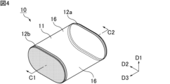
- FIG. 4 is a schematic perspective view showing an example of the capacitor element shown in FIGS. 1, 2, and 3.
- FIG. FIG. 5 is a schematic cross-sectional view showing an example of a cross section of the capacitor element shown in FIG. 4 taken along line segment C1-C2.
- FIG. 1 is a schematic perspective view showing an example of a film capacitor according to a first embodiment of the present invention.
- FIG. 2 is a schematic cross-sectional view showing an example of a cross section of the film capacitor shown in FIG. 1 taken along line segment A1-A2.
- FIG. 3 is
- FIG. 6 is a schematic cross-sectional view showing another example of the cross section of the film capacitor shown in FIG. 1 taken along the line segment B1-B2.
- FIG. 7 is a schematic cross-sectional view showing an enlarged example of a region in the vicinity of the adhesive portion between the capacitor element and the exterior film in the film capacitor shown in FIG.
- FIG. 8 is a schematic cross-sectional view showing an example of a film capacitor according to the second embodiment of the present invention.
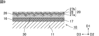
- FIG. 9 is a schematic cross-sectional view showing an enlarged example of a region in the vicinity of the adhesive portion between the capacitor element and the exterior film in the film capacitor shown in FIG.
- FIG. 10 is a schematic cross-sectional view showing an example of a film capacitor according to the third embodiment of the present invention.
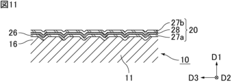
- FIG. 11 is a schematic cross-sectional view showing an enlarged example of a region in the vicinity of the adhesive portion between the capacitor element and the exterior film in the film capacitor shown in FIG.
- FIG. 12 is a schematic cross-sectional view showing an example of a film capacitor according to the fourth embodiment of the present invention.
- FIG. 13 is a schematic cross-sectional view showing an enlarged example of a region in the vicinity of the adhesive portion between the capacitor element and the exterior film in the film capacitor shown in FIG.
- FIG. 14 is a schematic cross-sectional view showing an example of a film capacitor according to the fifth embodiment of the present invention.
- the film capacitor of the present invention will be described below. Note that the present invention is not limited to the following configuration, and may be modified as appropriate without departing from the gist of the present invention. In addition, a combination of multiple individual preferred configurations described below also constitutes the present invention.
- each embodiment will simply be referred to as the "film capacitor of the present invention.”
- the film capacitor of the present invention comprises a capacitor element having a body including a dielectric film and an electrode layer, and external electrodes provided on the end faces of the body, and an exterior film enclosing the capacitor element, the capacitor element having a resin film exposed on the surface of the exterior film at a position other than the external electrodes, the exterior film having a thermoplastic resin layer exposed on the surface of the capacitor element, and the resin film of the capacitor element and the thermoplastic resin layer of the exterior film are bonded together.
- the dielectric film is a resin film.
- FIG. 1 is a schematic perspective view showing an example of a film capacitor according to a first embodiment of the present invention.
- FIG. 2 is a schematic cross-sectional view showing an example of a cross-section along line segment A1-A2 of the film capacitor shown in FIG. 1.
- FIG. 3 is a schematic cross-sectional view showing an example of a cross-section along line segment B1-B2 of the film capacitor shown in FIG. 1.
- the film capacitor 1 shown in Figures 1, 2, and 3 has a capacitor element 10 and an exterior film 20.
- the first direction D1, the second direction D2, and the third direction D3 are perpendicular to each other.
- FIG. 4 is a schematic perspective view showing an example of the capacitor element shown in FIGS. 1, 2, and 3.
- FIG. 5 is a schematic cross-sectional view showing an example of a cross-section along line segment C1-C2 of the capacitor element shown in FIG. 4.
- the capacitor element 10 shown in Figures 4 and 5 has a body 11, a first external electrode 12a, and a second external electrode 12b.
- the element body 11 includes a dielectric film and an electrode layer.
- the base body 11 has a metallized film including a dielectric film and an electrode layer.
- the base body 11 is a wound body in which a first metallized film 13a and a second metallized film 13b are wound in a stacked state in a first direction D1.
- the film capacitor 1, specifically the capacitor element 10 is a wound-type film capacitor in which the metallized films are wound in a stacked state.
- the film capacitor 1, specifically the capacitor element 10 may be a laminated film capacitor (e.g., rectangular) in which metallized films are laminated.
- element body 11 has a flat cross-sectional shape when viewed in a cross section perpendicular to the winding axis direction of element body 11 (third direction D3 in Figures 4 and 5). Specifically, it is preferable that element body 11 is pressed into a flat shape such as an ellipse or oval, and that the cross-sectional shape of element body 11 is thinner than when it is a perfect circle.
- Whether the base body has been pressed to have a flat cross-sectional shape can be confirmed, for example, by checking whether or not there are press marks on the base body.
- the capacitor element 10 may have a cylindrical winding axis.
- the winding axis is disposed on the central axis of the first metallized film 13a and the second metallized film 13b in the wound state, and serves as the winding axis when winding the first metallized film 13a and the second metallized film 13b.
- the first metallized film 13a has a first dielectric film 14a as a dielectric film and a first metal layer 15a as an electrode layer.
- the first dielectric film 14a has a first principal surface 14aa and a second principal surface 14ab that face each other in the first direction D1.
- the first metal layer 15a is provided on the first main surface 14aa of the first dielectric film 14a. Specifically, the first metal layer 15a is provided on the first main surface 14aa of the first dielectric film 14a so as to reach one side edge of the first dielectric film 14a in the third direction D3, but not to reach the other side edge of the first dielectric film 14a.
- the second metallized film 13b has a second dielectric film 14b as a dielectric film and a second metal layer 15b as an electrode layer.
- the second dielectric film 14b has a first main surface 14ba and a second main surface 14bb that face each other in the first direction D1.
- the second metal layer 15b is provided on the first main surface 14ba of the second dielectric film 14b. Specifically, the second metal layer 15b is provided on the first main surface 14ba of the second dielectric film 14b so as not to reach one side edge of the second dielectric film 14b in the third direction D3, but to reach the other side edge of the second dielectric film 14b.
- adjacent first metallized films 13a and second metallized films 13b are shifted in the third direction D3 so that the end of the first metal layer 15a that reaches the side edge of the first dielectric film 14a is exposed on one end face of the element body 11, and the end of the second metal layer 15b that reaches the side edge of the second dielectric film 14b is exposed on the other end face of the element body 11.
- the first metallized film 13a protrudes toward the first external electrode 12a relative to the second metallized film 13b.
- the second metallized film 13b protrudes toward the second external electrode 12b relative to the first metallized film 13a.
- the first metal layer 15a is connected to the first external electrode 12a and is not connected to the second external electrode 12b.
- the second metal layer 15b is connected to the second external electrode 12b and is not connected to the first external electrode 12a.
- the adjacent first metallized film 13a and second metallized film 13b are shifted in the third direction D3 as described above, so that in the adjacent first dielectric film 14a and second dielectric film 14b, the first dielectric film 14a having the first metal layer 15a on the first main surface 14aa protrudes toward the first external electrode 12a relative to the second dielectric film 14b having the first metal layer 15a not provided on its main surface. Also, in the adjacent first dielectric film 14a and second dielectric film 14b, the second dielectric film 14b having the second metal layer 15b on the first main surface 14ba protrudes toward the second external electrode 12b relative to the first dielectric film 14a having the second metal layer 15b not provided on its main surface.
- the element body 11 is formed by winding the first metallized film 13a and the second metallized film 13b in a stacked state in the first direction D1, and therefore can be said to include the first dielectric film 14a, the first metal layer 15a, the second dielectric film 14b, and the second metal layer 15b in the first direction D1. It can also be said that the element body 11 is a wound body formed by winding the first dielectric film 14a, the first metal layer 15a, the second dielectric film 14b, and the second metal layer 15b in the first direction D1.
- the first main surface 14aa of the first dielectric film 14a and the second main surface 14bb of the second dielectric film 14b face each other in the first direction D1
- the second main surface 14ab of the first dielectric film 14a and the first main surface 14ba of the second dielectric film 14b face each other in the first direction D1.
- the first metallized film 13a and the second metallized film 13b are wound in a state in which they are stacked in the first direction D1.
- the first metallized film 13a and the second metallized film 13b are wound in a state in which they are stacked in the first direction D1, so that the second metallized film 13b is on the inside of the first metallized film 13a, specifically, the first metal layer 15a is on the inside of the first dielectric film 14a, and the second metal layer 15b is on the inside of the second dielectric film 14b. That is, in the element body 11, the first metal layer 15a and the second metal layer 15b face each other with the first dielectric film 14a or the second dielectric film 14b sandwiched between them.
- the first metal layer 15a may be provided with a fuse portion.
- the fuse portion provided in the first metal layer 15a is, for example, a portion of the first metal layer 15a that connects a divided electrode portion in which a portion facing the second metal layer 15b is divided into multiple portions, and an electrode portion that does not face the second metal layer 15b.
- Examples of electrode patterns of the first metal layer 15a provided with a fuse portion include the electrode patterns disclosed in JP 2004-363431 A and JP 5-251266 A.
- the second metal layer 15b may also be provided with a fuse portion, similar to the first metal layer 15a.
- the first dielectric film 14a may contain a curable resin as a main component.
- the main component means the component with the highest weight percentage, preferably the component with a weight percentage greater than 50% by weight.
- the curable resin may be a thermosetting resin or a photocurable resin.
- thermosetting resin means a resin that can be cured by heat, but the curing method is not limited. Therefore, thermosetting resin also includes resins that can be cured by methods other than heat (e.g., light, electron beam, etc.) so long as they are heat-curable. Also, depending on the material, a reaction may be initiated due to the reactivity of the material itself, and resins that proceed to cure without necessarily being subjected to heat from the outside are also considered to be thermosetting resins. The same applies to photocurable resins, and so long as they are light-curable, they also include resins that can be cured by methods other than light (e.g., heat, etc.).
- the curable resin is preferably made of a cured product of a first organic material having a hydroxyl group (OH group) and a second organic material having an isocyanate group (NCO group).
- the curable resin is made of a cured product having a urethane bond obtained by reacting the hydroxyl group of the first organic material with the isocyanate group of the second organic material.
- FT-IR Fourier transform infrared spectrophotometer
- the first dielectric film 14a may contain at least one of a hydroxyl group and an isocyanate group.
- the first dielectric film 14a may contain either a hydroxyl group or an isocyanate group, or may contain both a hydroxyl group and an isocyanate group.
- Examples of the first organic material include phenoxy resin, polyvinyl acetoacetal resin, polyvinyl butyral resin, etc.
- the second organic material examples include aromatic polyisocyanates such as diphenylmethane diisocyanate (MDI) and tolylene diisocyanate (TDI), and aliphatic polyisocyanates such as hexamethylene diisocyanate (HDI).
- aromatic polyisocyanates such as diphenylmethane diisocyanate (MDI) and tolylene diisocyanate (TDI)
- aliphatic polyisocyanates such as hexamethylene diisocyanate (HDI).
- HDI hexamethylene diisocyanate
- the first dielectric film 14a may contain a thermoplastic resin as a main component.
- thermoplastic resins examples include polypropylene resin, polyethersulfone resin, polyetherimide resin, polyarylate resin, etc.
- the first dielectric film 14a may contain additives to impart various functions.
- Additives include, for example, leveling agents to impart smoothness.
- the additive preferably has a functional group that reacts with a hydroxyl group and/or an isocyanate group and forms part of the crosslinked structure of the cured product.
- examples of such additives include resins having at least one functional group selected from the group consisting of a hydroxyl group, an epoxy group, a silanol group, and a carboxyl group.
- the second dielectric film 14b may contain a thermosetting resin as a main component, a photocurable resin as a main component, or a thermoplastic resin as a main component.
- the second dielectric film 14b may also contain an additive, like the first dielectric film 14a.
- compositions of the first dielectric film 14a and the second dielectric film 14b may be different from each other, but are preferably the same.
- the thickness of the first dielectric film 14a and the second dielectric film 14b is preferably 1 ⁇ m or more and 10 ⁇ m or less, and more preferably 3 ⁇ m or more and 5 ⁇ m or less.
- the thicknesses of the first dielectric film 14a and the second dielectric film 14b may be different from each other, but it is preferable that they are the same.
- the thickness of the dielectric film is measured using an optical thickness gauge.
- the first dielectric film 14a and the second dielectric film 14b are each preferably produced by forming a resin solution containing the resin material as described above into a film and then curing it by heat treatment.
- Examples of materials that can be used to form the first metal layer 15a and the second metal layer 15b include metals such as aluminum, zinc, titanium, magnesium, tin, and nickel.
- compositions of the first metal layer 15a and the second metal layer 15b may be different from each other, but are preferably the same.
- the thickness of the first metal layer 15a and the second metal layer 15b is preferably 5 nm or more and 40 nm or less.
- the thicknesses of the first metal layer 15a and the second metal layer 15b may be different from each other, but are preferably the same.
- the thickness of the metal layer is measured by observing a cross section of the metallized film along the first direction using a transmission electron microscope (TEM).
- TEM transmission electron microscope
- the first metal layer 15a and the second metal layer 15b are preferably formed by depositing a metal such as that described above onto the main surfaces of the first dielectric film 14a and the second dielectric film 14b, respectively.
- the base body 11 may include one metallized film.
- the base body 11 may include a metallized film having a first dielectric film 14a in which a first metal layer 15a is provided on a first main surface 14aa and a second metal layer 15b is provided on a second main surface 14ab, and a second dielectric film 14b in which no metal layer is provided.
- the base body 11 may include a metallized film having a second dielectric film 14b in which a first metal layer 15a is provided on a second main surface 14bb and a second metal layer 15b is provided on a first main surface 14ba, and a first dielectric film 14a in which no metal layer is provided.
- the first external electrode 12a is provided on one end surface of the element body 11. Specifically, the first external electrode 12a is connected to the first metal layer 15a by contacting the end of the first metal layer 15a exposed on one end surface of the element body 11. On the other hand, the first external electrode 12a is not connected to the second metal layer 15b.
- the second external electrode 12b is provided on the other end surface of the element body 11. Specifically, the second external electrode 12b is connected to the second metal layer 15b by contacting the end of the second metal layer 15b exposed on the other end surface of the element body 11. On the other hand, the second external electrode 12b is not connected to the first metal layer 15a.
- the constituent materials of the first external electrode 12a and the second external electrode 12b include metals such as zinc, aluminum, tin, and zinc-aluminum alloys.
- compositions of the first external electrode 12a and the second external electrode 12b may be different from each other, but are preferably the same.
- the first external electrode 12a and the second external electrode 12b are preferably formed by spraying a metal such as that described above onto one end face and the other end face of the body 11, respectively.
- the exterior film 20 contains the capacitor element 10. Specifically, an internal space is provided in the exterior film 20, and the capacitor element 10 is housed in the internal space of the exterior film 20.
- the exterior film 20 is composed of a first exterior film material 21a and a second exterior film material 21b.
- the first exterior film material 21a and the second exterior film material 21b are molded into a cup shape to match the outer shape of the capacitor element 10.
- the first exterior film material 21a and the second exterior film material 21b may each have a first flange portion 22a and a second flange portion 22b on the outer edge (four sides in the example shown in FIG. 1).
- the first exterior film material 21a and the second exterior film material 21b may seal the capacitor element 10 by heat welding the first flange portion 22a and the second flange portion 22b.
- the thickness of the exterior film 20 is preferably 80 ⁇ m or more and 200 ⁇ m or less, and more preferably 100 ⁇ m or more and 160 ⁇ m or less.
- the thickness of the exterior film 20 is less than 80 ⁇ m, the strength of the exterior film 20 will be low and the exterior film 20 may become more susceptible to damage.
- the thickness of the exterior film 20 is greater than 200 ⁇ m, the workability of the exterior film 20 may decrease. In addition, if the thickness of the exterior film 20 is greater than 200 ⁇ m, the size of the exterior film 20 will be large, which may make it difficult to miniaturize the film capacitor 1.
- the capacitor element 10 has a resin film 16 exposed on the surface facing the exterior film 20 at a position other than the first external electrode 12a and the second external electrode 12b.
- the resin film 16 corresponds to the first dielectric film 14a.
- the first dielectric film 14a constitutes the resin film 16.
- the exterior film 20 has a thermoplastic resin layer 26 exposed on the surface facing the capacitor element 10.
- the melting point of the thermoplastic resin layer 26 of the exterior film 20 is preferably lower than the melting point of the resin film 16 of the capacitor element 10. In this case, when storing the capacitor element 10 in the internal space of the exterior film 20, for example, even if an attempt is made to heat-seal the first flange portion 22a of the first exterior film material 21a and the second flange portion 22b of the second exterior film material 21b, melting of the resin film 16 of the capacitor element 10 is suppressed during the heat-sealing.
- the resin film 16 of the capacitor element 10 (in the example shown in FIG. 5, the first dielectric film 14a) and the thermoplastic resin layer 26 of the exterior film 20 are bonded together by an adhesive 30.
- the adhesive 30 is provided in the gap between the capacitor element 10 and the exterior film 20, so the occurrence of a gap between the capacitor element 10 and the exterior film 20 is suppressed. Furthermore, even if the exterior film 20 attempts to expand due to an increase in pressure in the internal space of the exterior film 20 when the film capacitor 1 is used in a high-temperature environment, the exterior film 20 is adhered to the capacitor element 10 by the adhesive 30, so the occurrence of a gap between the capacitor element 10 and the exterior film 20 is suppressed.
- the occurrence of gaps between the capacitor element 10 and the exterior film 20 is suppressed, thereby suppressing the deterioration of heat dissipation caused by the gaps.
- the adhesive 30 preferably has excellent adhesion and durability in high-temperature environments.
- materials that can be used for such adhesive 30 include epoxy resin, urethane resin, phenolic resin, silicone resin, etc.
- a polypropylene resin layer may be used as the adhesive 30.
- thermoplastic resin layer 26 of the exterior film 20 is adhered to the entire surface of the resin film 16 of the capacitor element 10, as shown in Figures 2 and 3.
- adhesive 30 covers the entire surface of the resin film 16 of the capacitor element 10, as shown in Figures 2 and 3.
- FIG. 6 is a schematic cross-sectional view showing another example of a cross section along line segment B1-B2 of the film capacitor shown in FIG. 1.
- thermoplastic resin layer 26 of the exterior film 20 may be adhered to a portion of the surface of the resin film 16 of the capacitor element 10.
- the adhesive 30 may cover a portion of the surface of the resin film 16 of the capacitor element 10.
- thermoplastic resin layer 26 of the exterior film 20 is adhered to at least the flat portion of the surface of the resin film 16 of the capacitor element 10 by an adhesive 30.
- Figure 7 is a schematic cross-sectional view showing an enlarged example of the area near the adhesive joint between the capacitor element and the exterior film in the film capacitor shown in Figure 2.
- the surface of the thermoplastic resin layer 26 of the exterior film 20 facing the resin film 16 has an uneven shape.
- thermoplastic resin layer 26 of the exterior film 20 on the side of the resin film 16 is uneven, the adhesion area between the thermoplastic resin layer 26 of the exterior film 20 and the adhesive 30 tends to increase, and the adhesive strength between the two tends to improve. As a result, the adhesive strength between the resin film 16 of the capacitor element 10 and the thermoplastic resin layer 26 of the exterior film 20 tends to improve.
- the surface of the thermoplastic resin layer 26 of the exterior film 20 on the side of the resin film 16 has an uneven shape, the surface area of the exterior film 20 tends to increase, which tends to improve the heat dissipation properties of the exterior film 20.
- the multiple recesses or protrusions present on that surface may be arranged regularly or irregularly.
- the multiple recesses or protrusions present on that surface may be arranged in a line or in a dot pattern.
- the heights of the multiple protrusions present on the surface of the thermoplastic resin layer 26 of the exterior film 20 facing the resin film 16 may be the same as each other, may be different from each other, or may be partially different.
- the surface of the thermoplastic resin layer 26 of the exterior film 20 facing the resin film 16 has an uneven shape, which is achieved, for example, by subjecting the exterior film 20 to an uneven surface treatment in advance.
- thermoplastic resin layer 26 of the exterior film 20 facing the resin film 16 may not be uneven, but may be flat, for example.
- the surface of the exterior film 20 opposite the resin film 16 may have an uneven shape.
- the surface area of the exterior film 20 tends to increase, which tends to improve the heat dissipation properties of the exterior film 20.
- the surface of the exterior film 20 opposite the resin film 16 may not be uneven, but may be flat, for example.
- the surface of the resin film 16 of the capacitor element 10 facing the thermoplastic resin layer 26 may be uneven, or it may be flat, for example, as shown in FIG. 7.
- the exterior film 20 is preferably a laminate film including a first resin layer 27a, which is a thermoplastic resin layer 26, a metal layer 28, and a second resin layer 27b, which are laminated in this order from the capacitor element 10 side.
- the first resin layer 27a functions as a layer for thermally welding laminate films together, for example, a layer for thermally welding the first flange portion 22a of the first exterior film material 21a and the second flange portion 22b of the second exterior film material 21b.
- the first resin layer 27a is preferably made of a polyolefin-based thermoplastic resin such as polypropylene resin.
- the thickness of the first resin layer 27a is preferably 20 ⁇ m or more and 150 ⁇ m or less.
- the metal layer 28 functions as a layer to improve the barrier properties against moisture.
- the metal layer 28 is preferably made of aluminum.
- the thickness of the metal layer 28 is preferably 20 ⁇ m or more and 50 ⁇ m or less.
- the second resin layer 27b functions as a layer to protect the metal layer 28 and further improve the barrier properties against moisture.
- the second resin layer 27b is preferably made of a thermoplastic resin such as polyethylene terephthalate resin or nylon resin.
- the thickness of the second resin layer 27b is preferably 10 ⁇ m or more and 40 ⁇ m or less.
- the first resin layer 27a and the metal layer 28 may be bonded with an adhesive or may be thermocompression bonded.
- the second resin layer 27b and the metal layer 28 may be bonded with an adhesive or may be thermocompression bonded.
- the exterior film 20 may be composed of one layer or multiple layers, so long as it has a thermoplastic resin layer 26 exposed on the surface on the capacitor element 10 side. If the exterior film 20 is a laminate film composed of multiple layers, the number of layers is not particularly limited, and may be three layers as described above, or may be other than three layers.
- the film capacitor 1 may further have a first lead terminal 50a electrically connected to the first external electrode 12a.
- the first pull-out terminal 50a may be welded to the first external electrode 12a, or may be connected via a joining member such as solder.
- the film capacitor 1 may further have a second lead terminal 50b electrically connected to the second external electrode 12b.
- the second pull-out terminal 50b may be welded to the second external electrode 12b, or may be connected via a joining member such as solder.
- the first pull-out terminal 50a and the second pull-out terminal 50b are each used as terminals for electrically connecting the capacitor element 10 to an object to be mounted when mounting the film capacitor 1 to the object to be mounted.
- the constituent material of the first pull-out terminal 50a and the second pull-out terminal 50b may be, for example, a metal such as copper, oxygen-free copper, aluminum, or an alloy containing at least one of these.
- the constituent material of the first pull-out terminal 50a and the second pull-out terminal 50b is preferably copper or oxygen-free copper.
- the constituent material of the first pull-out terminal 50a and the second pull-out terminal 50b is a copper-based material
- oxygen-free copper copper: 99.96% by weight or more
- tough pitch copper copper: 99.90% by weight or more
- phosphorus-deoxidized copper copper: 99.90% by weight or more, phosphorus: 0.015% by weight or more, 0.040% by weight or less
- phosphorus: 0.015% by weight or more, 0.040% by weight or less etc.
- the first pull-out terminal 50a and the second pull-out terminal 50b may each have, for example, a plate shape or a line shape (rod shape). In this case, the first pull-out terminal 50a and the second pull-out terminal 50b may each have a shape with a partially bent portion.
- the exterior film 20 may be provided with a first pull-out opening 23a for pulling the first pull-out terminal 50a out of the exterior film 20.
- the exterior film 20 may be provided with a first pull-out opening 23a between the first flange portion 22a and the second flange portion 22b for pulling the first pull-out terminal 50a out of the exterior film 20.
- the exterior film 20 may be provided with a second pull-out opening 23b for pulling the second pull-out terminal 50b out of the exterior film 20.
- the exterior film 20 may be provided with a second pull-out opening 23b between the first flange portion 22a and the second flange portion 22b for pulling the second pull-out terminal 50b out of the exterior film 20.
- the film capacitor 1 may further include a first insulating film 60a provided between the exterior film 20 and the first pull-out terminal 50a.
- the first insulating film 60a may be provided between the first flange portion 22a of the exterior film 20 and the first pull-out terminal 50a, and between the second flange portion 22b of the exterior film 20 and the first pull-out terminal 50a.
- the first pull-out terminal 50a is fixed while being sealed by the first insulating film 60a.
- the first insulating film 60a covers the entire first pull-out terminal 50a at the first pull-out opening 23a of the exterior film 20.
- the first insulating film 60a is preferably adhered to the thermoplastic resin layer 26 of the exterior film 20 while being adhered to the first external electrode 12a.
- the film capacitor 1 may further include a second insulating film 60b provided between the exterior film 20 and the second pull-out terminal 50b.
- the second insulating film 60b may be provided between the first flange portion 22a of the exterior film 20 and the second pull-out terminal 50b, and between the second flange portion 22b of the exterior film 20 and the second pull-out terminal 50b.
- the second pull-out terminal 50b is fixed while being sealed by the second insulating film 60b.
- the second insulating film 60b covers the entire second pull-out terminal 50b at the second pull-out opening 23b of the exterior film 20.
- the second insulating film 60b is preferably adhered to the thermoplastic resin layer 26 of the exterior film 20 while being adhered to the second external electrode 12b.
- the first insulating film 60a and the second insulating film 60b are each preferably made of a polyolefin-based thermoplastic resin such as polypropylene resin.
- the capacitor element further has a protective film that covers the surfaces of the body other than the end faces, and the protective film constitutes a resin film.
- the film capacitor of embodiment 2 of the present invention is similar to the film capacitor of embodiment 1 of the present invention.
- FIG. 8 is a schematic cross-sectional view showing an example of a film capacitor according to embodiment 2 of the present invention.
- the capacitor element 10 further has a protective film 17 that covers the surfaces of the body 11 other than the end faces.
- the protective film 17 is preferably wrapped around the element 11 so as to cover the surface of the element 11 except for the end faces.
- the number of turns of the protective film 17 is not particularly limited, and the protective film 17 may be wrapped around the element 11 once or multiple times.
- the protective film 17 is preferably a resin film that does not have a conductive layer (e.g., a metal layer) on its surface.
- a conductive layer e.g., a metal layer
- protective film 17 may be a resin film with a conductive layer provided on its surface.
- the conductive layer of protective film 17 functions as a layer for improving the barrier properties against moisture.
- the protective film 17 may be a resin film with adhesive.
- the protective film 17 may be in the form of a single sheet or may be divided into multiple sheets.
- thermoplastic resins such as polypropylene resin and polyethylene terephthalate resin.
- the material of the protective film 17 may be the same as or different from the material of the dielectric film of the base body 11, in this case the first dielectric film 14a and the second dielectric film 14b.
- the material of the protective film 17 may be the same as or different from the material of the thermoplastic resin layer 26 of the exterior film 20.
- the resin film 16 exposed on the surface of the capacitor element 10 facing the exterior film 20 corresponds to the protective film 17.
- the protective film 17 constitutes the resin film 16.
- the resin film 16 of the capacitor element 10, here the protective film 17, and the thermoplastic resin layer 26 of the exterior film 20 are bonded together with an adhesive 30.
- the film capacitor 2 like the film capacitor 1, the occurrence of gaps between the capacitor element 10 and the exterior film 20 is suppressed, and the deterioration of heat dissipation caused by the gaps is suppressed.
- Figure 9 is a schematic cross-sectional view showing an enlarged example of the area near the adhesive joint between the capacitor element and the exterior film in the film capacitor shown in Figure 8.
- the surface of the thermoplastic resin layer 26 of the exterior film 20 on the resin film 16 side, here the surface on the protective film 17 side has an uneven shape.
- the adhesive strength between the resin film 16 of the capacitor element 10 and the thermoplastic resin layer 26 of the exterior film 20, here the adhesive strength between the protective film 17 of the capacitor element 10 and the thermoplastic resin layer 26 of the exterior film 20 is likely to be improved, and further the heat dissipation properties of the exterior film 20 are likely to be improved.
- the surface of the protective film 17 of the capacitor element 10 facing the thermoplastic resin layer 26 may be uneven, or it may be flat, for example, as shown in FIG. 9.
- the dielectric film is a resin film.
- the film capacitor of embodiment 3 of the present invention is similar to the film capacitor of embodiment 1 of the present invention.
- FIG. 10 is a schematic cross-sectional view showing an example of a film capacitor according to embodiment 3 of the present invention.
- the resin film 16 of the capacitor element 10 and the thermoplastic resin layer 26 of the exterior film 20 are bonded by thermal welding.
- the film capacitor 3 like the film capacitor 1, the occurrence of gaps between the capacitor element 10 and the exterior film 20 is suppressed, and the deterioration of heat dissipation due to the influence of the gaps is suppressed.
- film capacitor 3 which uses thermal welding
- resin film 16 of capacitor element 10 and thermoplastic resin layer 26 of exterior film 20 can be bonded together without using adhesive as in film capacitor 1.
- film capacitor 3 which uses thermal welding is industrially useful because it does not require adhesive application steps, adhesive curing steps, etc. in the manufacturing process, compared to film capacitor 1, which uses adhesive.
- the heat-sealed portion between the resin film 16 of the capacitor element 10 and the thermoplastic resin layer 26 of the exterior film 20 extends over the entire surface of the resin film 16 of the capacitor element 10.
- the heat-sealed portion between the resin film 16 of the capacitor element 10 and the thermoplastic resin layer 26 of the exterior film 20 may extend over a portion of the surface of the resin film 16 of the capacitor element 10.
- thermoplastic resin layer 26 of the exterior film 20 is adhered by thermal welding to at least the flat portion of the surface of the resin film 16 of the capacitor element 10.
- FIG. 11 is a schematic cross-sectional view showing an enlarged example of a region near the adhesive portion between the capacitor element and the exterior film in the film capacitor shown in FIG. 10.
- thermoplastic resin layer 26 of the exterior film 20 when the resin film 16 of the capacitor element 10 and the thermoplastic resin layer 26 of the exterior film 20 are bonded by thermal welding, it is preferable that the surface of the thermoplastic resin layer 26 of the exterior film 20 facing the resin film 16 has an uneven shape. In this case, the adhesive strength between the resin film 16 of the capacitor element 10 and the thermoplastic resin layer 26 of the exterior film 20 is likely to be improved, and further, the heat dissipation properties of the exterior film 20 are likely to be improved.
- the configuration in which the surface of the thermoplastic resin layer 26 of the exterior film 20 on the side of the resin film 16 has an uneven shape can be achieved, for example, by applying an uneven processing to the exterior film 20 in advance, or by pressing the exterior film 20 against the capacitor element 10 (element 11) with a heater or mold with an uneven surface and heat welding the two together.
- the surface of the resin film 16 of the capacitor element 10 facing the thermoplastic resin layer 26 may be uneven as shown in FIG. 11, or it may be flat, for example, without being uneven.
- the capacitor element further has a protective film that covers the surfaces of the body other than the end faces, and the protective film constitutes a resin film.
- the film capacitor of embodiment 4 of the present invention is similar to the film capacitor of embodiment 1 of the present invention.
- FIG. 12 is a schematic cross-sectional view showing an example of a film capacitor according to embodiment 4 of the present invention.
- the capacitor element 10 further has a protective film 17 that covers the surfaces of the body 11 other than the end faces.
- the resin film 16 exposed on the surface of the capacitor element 10 facing the exterior film 20 corresponds to the protective film 17.
- the protective film 17 constitutes the resin film 16.
- the resin film 16 of the capacitor element 10, here the protective film 17, and the thermoplastic resin layer 26 of the exterior film 20 are bonded by thermal welding.
- the film capacitor 4 like the film capacitor 1, the occurrence of gaps between the capacitor element 10 and the exterior film 20 is suppressed, and the deterioration of heat dissipation due to the influence of the gaps is suppressed.
- FIG. 13 is a schematic cross-sectional view showing an enlarged example of a region near the adhesive portion between the capacitor element and the exterior film in the film capacitor shown in FIG. 12.
- the surface of the thermoplastic resin layer 26 of the exterior film 20 on the resin film 16 side, here the surface on the protective film 17 side has an uneven shape.
- the adhesive strength between the resin film 16 of the capacitor element 10 and the thermoplastic resin layer 26 of the exterior film 20, here the adhesive strength between the protective film 17 of the capacitor element 10 and the thermoplastic resin layer 26 of the exterior film 20 is likely to be improved, and further the heat dissipation properties of the exterior film 20 are likely to be improved.
- the surface of the protective film 17 of the capacitor element 10 facing the thermoplastic resin layer 26 may be uneven as shown in FIG. 13, or it may be flat, for example, without being uneven.
- the film capacitor of embodiment 5 of the present invention is similar to the film capacitors of embodiments 1 to 4 of the present invention.
- a film capacitor of embodiment 2 of the present invention in which the external electrodes of the capacitor element and the thermoplastic resin layer of the exterior film are bonded with an adhesive is shown. Note that in the film capacitors of embodiments 1, 3, and 4 of the present invention, the external electrodes of the capacitor element and the thermoplastic resin layer of the exterior film may also be bonded with an adhesive.
- FIG. 14 is a schematic cross-sectional view showing an example of a film capacitor according to embodiment 5 of the present invention.
- the resin film 16 of the capacitor element 10, here the protective film 17, and the thermoplastic resin layer 26 of the exterior film 20 are bonded together with an adhesive 30. Furthermore, in the film capacitor 5, the first external electrode 12a of the capacitor element 10 and the thermoplastic resin layer 26 of the exterior film 20 are bonded together with an adhesive 30. Furthermore, in the film capacitor 5, the second external electrode 12b of the capacitor element 10 and the thermoplastic resin layer 26 of the exterior film 20 are bonded together with an adhesive 30.
- the occurrence of gaps is suppressed not only between the protective film 17 of the capacitor element 10 and the exterior film 20, but also between the first external electrode 12a of the capacitor element 10 and the exterior film 20, and between the second external electrode 12b of the capacitor element 10 and the exterior film 20. Therefore, in the film capacitor 5, the occurrence of gaps between the capacitor element 10 and the exterior film 20 is sufficiently suppressed compared to the film capacitor 2, and therefore the deterioration of heat dissipation due to the influence of the gaps is sufficiently suppressed.
- a capacitor element having an element body including a dielectric film and an electrode layer, and external electrodes provided on end faces of the element body; and an exterior film that encapsulates the capacitor element, the capacitor element has a resin film exposed on a surface of the exterior film side at a position other than the external electrode, the exterior film has a thermoplastic resin layer exposed on a surface on the capacitor element side, a film capacitor, characterized in that the resin film of the capacitor element and the thermoplastic resin layer of the exterior film are bonded to each other.
- thermoplastic resin layer of the exterior film on the resin film side has an uneven shape.
- thermoplastic resin layer of the exterior film is adhered to the entire surface of the resin film of the capacitor element.
- ⁇ 6> The film capacitor according to any one of ⁇ 1> to ⁇ 5>, wherein the dielectric film constitutes the resin film.
- the capacitor element further includes a protective film covering a surface of the body other than the end surface,
- ⁇ 8> The film capacitor according to any one of ⁇ 1> to ⁇ 7>, wherein the external electrode of the capacitor element and the thermoplastic resin layer of the exterior film are bonded to each other with an adhesive.
- the exterior film is a laminate film including a first resin layer, which is the thermoplastic resin layer, a metal layer, and a second resin layer, which are laminated in this order from the capacitor element side.
Landscapes
- Engineering & Computer Science (AREA)
- Power Engineering (AREA)
- Microelectronics & Electronic Packaging (AREA)
- Manufacturing & Machinery (AREA)
- Fixed Capacitors And Capacitor Manufacturing Machines (AREA)
Priority Applications (1)
| Application Number | Priority Date | Filing Date | Title |
|---|---|---|---|
| JP2025539147A JPWO2025032938A1 (https=) | 2023-08-07 | 2024-05-31 |
Applications Claiming Priority (2)
| Application Number | Priority Date | Filing Date | Title |
|---|---|---|---|
| JP2023-128649 | 2023-08-07 | ||
| JP2023128649 | 2023-08-07 |
Publications (1)
| Publication Number | Publication Date |
|---|---|
| WO2025032938A1 true WO2025032938A1 (ja) | 2025-02-13 |
Family
ID=94534575
Family Applications (1)
| Application Number | Title | Priority Date | Filing Date |
|---|---|---|---|
| PCT/JP2024/020035 Pending WO2025032938A1 (ja) | 2023-08-07 | 2024-05-31 | フィルムコンデンサ |
Country Status (2)
| Country | Link |
|---|---|
| JP (1) | JPWO2025032938A1 (https=) |
| WO (1) | WO2025032938A1 (https=) |
Citations (5)
| Publication number | Priority date | Publication date | Assignee | Title |
|---|---|---|---|---|
| JPS5324835U (https=) * | 1976-08-11 | 1978-03-02 | ||
| JP2002184642A (ja) * | 2000-12-11 | 2002-06-28 | Nichicon Corp | 乾式金属化フィルムコンデンサ |
| JP2005277101A (ja) * | 2004-03-24 | 2005-10-06 | Nippon Chemicon Corp | フィルムコンデンサ |
| JP2015070035A (ja) * | 2013-09-27 | 2015-04-13 | 株式会社日立メディコ | 高電圧コンデンサ及びその高電圧コンデンサを用いた高電圧発生装置 |
| WO2021149440A1 (ja) * | 2020-01-24 | 2021-07-29 | 株式会社デンソー | コンデンサモジュールおよび電力変換装置 |
-
2024
- 2024-05-31 WO PCT/JP2024/020035 patent/WO2025032938A1/ja active Pending
- 2024-05-31 JP JP2025539147A patent/JPWO2025032938A1/ja active Pending
Patent Citations (5)
| Publication number | Priority date | Publication date | Assignee | Title |
|---|---|---|---|---|
| JPS5324835U (https=) * | 1976-08-11 | 1978-03-02 | ||
| JP2002184642A (ja) * | 2000-12-11 | 2002-06-28 | Nichicon Corp | 乾式金属化フィルムコンデンサ |
| JP2005277101A (ja) * | 2004-03-24 | 2005-10-06 | Nippon Chemicon Corp | フィルムコンデンサ |
| JP2015070035A (ja) * | 2013-09-27 | 2015-04-13 | 株式会社日立メディコ | 高電圧コンデンサ及びその高電圧コンデンサを用いた高電圧発生装置 |
| WO2021149440A1 (ja) * | 2020-01-24 | 2021-07-29 | 株式会社デンソー | コンデンサモジュールおよび電力変換装置 |
Also Published As
| Publication number | Publication date |
|---|---|
| JPWO2025032938A1 (https=) | 2025-02-13 |
Similar Documents
| Publication | Publication Date | Title |
|---|---|---|
| WO2019146755A1 (ja) | フィルムコンデンサ、及び、フィルムコンデンサ用の外装ケース | |
| JP7222489B2 (ja) | フィルムコンデンサ | |
| JP7083419B2 (ja) | ケースレスフィルムコンデンサ | |
| JP7794316B2 (ja) | コンデンサ、コンデンサバンク、及び、コンデンサ用外装ケース | |
| KR100357434B1 (ko) | 전자회로기판을밀봉및캡슐화하는적층체 | |
| WO2025032938A1 (ja) | フィルムコンデンサ | |
| US20250166919A1 (en) | Film capacitor | |
| WO2025047126A1 (ja) | コンデンサモジュール | |
| JPS63181411A (ja) | 積層フイルムコンデンサ | |
| JP2013038298A (ja) | フィルムコンデンサ | |
| JP7836998B2 (ja) | コンデンサ及びその製造方法 | |
| JP7698692B2 (ja) | コンデンサ | |
| US11978593B2 (en) | Film capacitor and exterior case for film capacitor | |
| US20220115183A1 (en) | Film capacitor | |
| WO2025126705A1 (ja) | コンデンサモジュール | |
| JPS60160145A (ja) | 混成集積回路のパツケ−ジング | |
| JP7244032B2 (ja) | フィルムコンデンサ | |
| JP7312261B2 (ja) | フィルムコンデンサ | |
| JP7839292B2 (ja) | コンデンサ | |
| WO2025141924A1 (ja) | コンデンサモジュール | |
| WO2025047116A1 (ja) | コンデンサモジュール | |
| JP7816550B2 (ja) | コンデンサ、コンデンサバンク、及び、コンデンサ用外装ケース | |
| US12406812B2 (en) | Film capacitor | |
| WO2021025025A1 (ja) | 樹脂多層基板および樹脂多層基板の製造方法 | |
| WO2025047029A1 (ja) | コンデンサ |
Legal Events
| Date | Code | Title | Description |
|---|---|---|---|
| 121 | Ep: the epo has been informed by wipo that ep was designated in this application |
Ref document number: 24851372 Country of ref document: EP Kind code of ref document: A1 |
|
| ENP | Entry into the national phase |
Ref document number: 2025539147 Country of ref document: JP Kind code of ref document: A |
|
| WWE | Wipo information: entry into national phase |
Ref document number: 2025539147 Country of ref document: JP |
|
| NENP | Non-entry into the national phase |
Ref country code: DE |