WO2025027845A1 - 半導体装置および半導体装置の製造方法 - Google Patents
半導体装置および半導体装置の製造方法 Download PDFInfo
- Publication number
- WO2025027845A1 WO2025027845A1 PCT/JP2023/028403 JP2023028403W WO2025027845A1 WO 2025027845 A1 WO2025027845 A1 WO 2025027845A1 JP 2023028403 W JP2023028403 W JP 2023028403W WO 2025027845 A1 WO2025027845 A1 WO 2025027845A1
- Authority
- WO
- WIPO (PCT)
- Prior art keywords
- slit
- pattern
- surface pattern
- semiconductor device
- insulating substrate
- Prior art date
- Legal status (The legal status is an assumption and is not a legal conclusion. Google has not performed a legal analysis and makes no representation as to the accuracy of the status listed.)
- Pending
Links
Images


Classifications
-
- H—ELECTRICITY
- H10—SEMICONDUCTOR DEVICES; ELECTRIC SOLID-STATE DEVICES NOT OTHERWISE PROVIDED FOR
- H10W—GENERIC PACKAGES, INTERCONNECTIONS, CONNECTORS OR OTHER CONSTRUCTIONAL DETAILS OF DEVICES COVERED BY CLASS H10
- H10W40/00—Arrangements for thermal protection or thermal control
- H10W40/10—Arrangements for heating
-
- H—ELECTRICITY
- H10—SEMICONDUCTOR DEVICES; ELECTRIC SOLID-STATE DEVICES NOT OTHERWISE PROVIDED FOR
- H10W—GENERIC PACKAGES, INTERCONNECTIONS, CONNECTORS OR OTHER CONSTRUCTIONAL DETAILS OF DEVICES COVERED BY CLASS H10
- H10W70/00—Package substrates; Interposers; Redistribution layers [RDL]
- H10W70/60—Insulating or insulated package substrates; Interposers; Redistribution layers
Definitions
- This disclosure relates to a semiconductor device and a method for manufacturing the semiconductor device.
- Patent Document 1 discloses a semiconductor device including a plurality of wiring layers (corresponding to a front surface pattern), an insulating substrate (corresponding to an insulating layer) to which the first rear surfaces of the plurality of wiring layers are bonded, a plurality of heat dissipation layers (corresponding to a rear surface pattern) whose second main surface is bonded to the insulating substrate, a semiconductor element bonded to any of the first main surfaces of the plurality of wiring layers, and a sealing resin that covers the insulating substrate, the plurality of wiring layers, and the semiconductor element.
- the plurality of wiring layers bonded to the front surface of the insulating substrate and the plurality of heat dissipation layers bonded to the rear surface of the insulating substrate so as to overlap when viewed in the thickness direction of the insulating substrate, the difference in the amount of expansion and contraction between the front surface side and the rear surface side of the insulating substrate due to temperature changes is reduced, thereby suppressing warping that occurs in the insulating substrate.
- Patent Document 1 does not take into consideration the warping of the product that occurs after transfer molding.
- the slits that divide the insulating substrate into multiple wiring layers on the front side and the slits that divide the insulating substrate into multiple heat dissipation layers on the back side are in the same position when viewed from the thickness direction of the insulating substrate, which causes the entire substrate including the multiple wiring layers and multiple heat dissipation layers to bend and crack easily.
- the present disclosure therefore aims to provide a technology that can prevent the insulating substrate from cracking even if the product warps after transfer molding.
- the semiconductor device comprises an insulating substrate having an insulating layer, a surface pattern formed on the surface of the insulating layer, and a back surface pattern formed on the back surface of the insulating layer, a semiconductor element mounted on the surface pattern, and a sealing resin that seals the insulating substrate and the semiconductor element while exposing a surface of the back surface pattern opposite to a surface facing the insulating layer, the back surface pattern is soldered to a heat sink, the surface of the back surface pattern that is joined to the heat sink is located at the same height as the surface of the sealing resin that faces the heat sink, the front surface pattern is provided with a first slit for dividing the front surface pattern into a plurality of regions, and the back surface pattern is provided with a second slit for dividing the back surface pattern into a plurality of regions, and the first slit and the second slit do not overlap or only partially overlap when viewed from the thickness direction of the insulating substrate.
- the overlapping portion between the first slit on the front side of the insulating substrate and the second slit on the back side is reduced, so that even if the product warps after transfer molding, cracking of the insulating substrate can be suppressed.
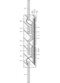
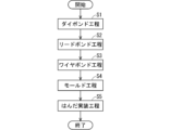
- 1 is a cross-sectional view of a semiconductor device according to an embodiment; 1 is a flowchart showing a method for manufacturing a semiconductor device according to an embodiment.
- 4A to 4C are cross-sectional views showing a die bonding step in the embodiment.
- 5A to 5C are cross-sectional views showing a lead bonding process in the embodiment.
- 4A to 4C are cross-sectional views showing a wire bonding step in the embodiment.
- 4A to 4C are cross-sectional views showing a molding process in the embodiment.
- 4A to 4C are cross-sectional views showing a solder mounting process in the embodiment.
- FIG. 1 is a cross-sectional view of a semiconductor device for explaining the occurrence of solder voids in an embodiment
- 2 is a bottom view illustrating an example of an insulating substrate included in the semiconductor device according to the embodiment
- FIG. 11 is a bottom view showing another example of an insulating substrate included in the semiconductor device according to the embodiment.
- FIG. 4 is an enlarged cross-sectional view of the periphery of a second slit provided in a back surface pattern of the semiconductor device according to the embodiment
- 13 is an enlarged cross-sectional view of the periphery of a second slit provided in a back surface pattern of a semiconductor device according to a modified example of the embodiment
- FIG. 1 is a cross-sectional view of a semiconductor device for explaining the occurrence of solder voids in a related art.
- the semiconductor device includes an insulating substrate 1, a plurality of semiconductor elements 2, a plurality of lead frames 3, and a molded resin 5 as a sealing resin.
- the insulating substrate 1 includes an insulating layer 1a, a surface pattern 1b, and a back pattern 1c.
- the insulating layer 1a is made of ceramics.
- the surface pattern 1b is made of a metal such as copper or aluminum, and is formed on the surface of the insulating layer 1a.
- the surface pattern 1b is provided with a first slit 6 for dividing the surface pattern 1b into a plurality of regions.
- the back pattern 1c is made of a metal such as copper or aluminum, and is formed on the back surface of the insulating layer 1a.
- the back pattern 1c is provided with a second slit 7 for dividing the back pattern 1c into a plurality of regions.
- the second slit 7 is provided in a lattice shape when viewed from the thickness direction of the insulating substrate 1.
- the second slit 7 is also provided so as to surround the periphery of the semiconductor element 2 when viewed from the thickness direction of the insulating substrate 1.
- the multiple semiconductor elements 2 are mounted on the surface pattern 1b via solder 4.
- the multiple semiconductor elements 2 are elements that function as, for example, switching elements or rectifying elements.
- the switching elements are, for example, IGBTs (Insulated Gate Bipolar Transistors) or MOSFETs (Metal-Oxide-Semiconductor Field-Effect Transistors).
- the rectifying elements are diode elements.
- the material constituting the multiple semiconductor elements 2 is, for example, silicon (Si).
- the material constituting the multiple semiconductor elements 2 is not limited to silicon, and may be, for example, a wide bandgap semiconductor material such as silicon carbide (SiC), gallium nitride (GaN), or diamond (C).
- a wide bandgap semiconductor material is a material that has a bandgap wider than that of Si.
- the multiple semiconductor elements 2 made of a wide bandgap semiconductor material are capable of operating using a large current and in a high-temperature environment. For this reason, it is preferable that the material constituting the multiple semiconductor elements 2 is a wide bandgap semiconductor material.
- the material of the multiple lead frames 3 is, for example, copper.
- the multiple lead frames 3 are joined to the surface electrodes of the semiconductor element 2 by solder 4, joined to the surface pattern 1b by solder 4, or connected to the wire pads of the semiconductor element 2 via aluminum wires 8.
- the molded resin 5 is, for example, an epoxy-based thermosetting resin.
- the molded resin 5 seals the insulating substrate 1 and the semiconductor element 2 while leaving the surface of the back pattern 1c opposite the surface facing the insulating layer 1a exposed.
- the semiconductor device is bonded to a heat sink 10 (see FIG. 7), but the surface of the back pattern 1c that is bonded to the heat sink 10 is located at the same height as the surface of the molded resin 5 that faces the heat sink 10, so no step is created between the back pattern 1c and the molded resin 5.
- Figure 2 is a flow chart showing a method for manufacturing a semiconductor device according to an embodiment.
- Figure 3 is a cross-sectional view showing a die bonding process in the embodiment.
- Figure 4 is a cross-sectional view showing a lead bonding process in the embodiment.
- Figure 5 is a cross-sectional view showing a wire bonding process in the embodiment.
- Figure 6 is a cross-sectional view showing a molding process in the embodiment.
- Figure 7 is a cross-sectional view showing a solder mounting process in the embodiment. Note that Figure 2 is a simplified illustration of only the main steps of the method for manufacturing a semiconductor device.
- step S1 solder 4 is placed on the surface pattern 1b of the insulating substrate 1, the semiconductor element 2 is mounted thereon, and the solder 4 is melted by reflow or the like to bond the semiconductor element 2 to the insulating substrate 1.
- bonding with solder 4 is given as an example, but this is not limiting, and sintering with silver or copper may also be performed.
- step S2 solder 4 is placed on the surface electrodes of the semiconductor element 2 and on the surface pattern 1b, and the lead frame 3 is placed on top of them.
- the solder 4 is melted by reflow or the like, thereby joining the surface electrodes of the semiconductor element 2 to the lead frame 3 and also joining the surface pattern 1b to the lead frame 3.
- step S3 the wire pads of the semiconductor element 2 and the signal terminals of the lead frame 3 are ultrasonically bonded with aluminum wires 8 having a wire diameter of approximately 100 to 400 ⁇ m.
- step S4 the wire-bonded product and tablet-shaped resin that will be the material for molded resin 5 are placed in the lower die of a metal mold (not shown), the upper die is closed, and the resin is gelled at a high temperature of about 180°C, and pressure is applied to force it through the runner and gate into the space (cavity) within the metal mold. The gelled resin hardens again at high temperature to become molded resin 5 that has the same shape as the cavity. This is then removed from the metal mold.
- step S5 solder 11 and the semiconductor device, which is a molded product, are placed on the heat sink 10, which is a heat dissipation member, and the solder 11 is melted by reflow or the like to join the semiconductor device and the heat sink 10.
- the insulating substrate 1 is exposed to high temperatures in the die bonding process (step S1), lead bonding process (step S2), molding process (step S4), and solder mounting process (step S5).
- the ceramics that make up the insulating layer 1a of the insulating substrate 1 are brittle materials and have low bending resistance, so it is important to minimize warping in each process.
- the front and back patterns 1b and 1c are bonded and patterned on the front and back surfaces, respectively.
- Copper is generally used for the front and back patterns 1b and 1c because of its superior performance. Copper is a highly rigid material and has a different linear expansion coefficient from ceramics, so if the balance between the front and back sides of the insulating layer 1a is poor, warping will occur with temperature changes.
- the front pattern 1b is generally divided into multiple regions by first slits 6 to allow electrical conductivity, and is less rigid than the undivided front pattern 1b.
- second slits 7 are provided in the back pattern 1c to reduce its rigidity.
- the second slits 7 are not provided directly below the semiconductor element 2, but are provided around the area directly below the semiconductor element 2. In other words, the second slits 7 are provided so as to surround the area of the front surface pattern 1b that corresponds to the location where the semiconductor element 2 is mounted.
- Figure 13 is a cross-sectional view of a semiconductor device to explain the occurrence of solder voids 12 in related technology.
- Figure 8 is a cross-sectional view of a semiconductor device to explain the occurrence of solder voids 12 in an embodiment.
- solder void 12 If air is entrained during soldering to the heat sink 10 and remains in the solder 11, as shown in FIG. 13, it becomes a solder void 12 that inhibits heat dissipation.
- the solder void 12 can be discharged to the second slit 7 provided in the back pattern 1c as shown in FIG.
- the effect on heat dissipation is reduced, and a semiconductor device with good heat dissipation can be realized. Since the position where the solder void 12 occurs is not specific, the effect of discharging the solder void 12 from directly below the semiconductor element 2 is further enhanced by creating a reduced pressure atmosphere or rocking.
- the width of the connected portion of the outermost periphery of the back pattern 1c depends on the pressure when the resin is injected and the flatness of the insulating substrate 1, but it is preferable for it to be about 1 mm.
- FIG. 9 is a bottom view showing an example of an insulating substrate 1 included in a semiconductor device according to an embodiment.
- FIG. 10 is a bottom view showing another example of an insulating substrate 1 included in a semiconductor device according to an embodiment.
- FIG. 9 if the outermost periphery of the back surface pattern 1c is not connected, it is necessary to suppress the inflow of resin from the outermost periphery of the back surface pattern 1c by pressing a cushioning sheet or the like against the back surface pattern 1c during transfer molding, but this becomes more difficult as the thickness of the back surface pattern 1c increases.
- FIG. 9 is a bottom view showing an example of an insulating substrate 1 included in a semiconductor device according to an embodiment.
- the back surface pattern 1c is connected, so that a cushioning sheet or the like is not required, making it possible to suppress the inflow of resin without any restrictions on the thickness of the back surface pattern 1c.
- warping of the insulating substrate 1 alone is suppressed, but it is also important to suppress cracking of the insulating substrate 1 if warping occurs in the product after transfer molding. Warping of the product after transfer molding is caused by differences in expansion and contraction between the mold resin 5 and the insulating substrate 1. Therefore, it is important to make the linear expansion coefficients of the mold resin 5 and the insulating substrate 1 close to each other.
- the main components that determine the mechanical properties such as the linear expansion coefficient of the mold resin 5 are resin and filler, and the linear expansion coefficient can be reduced by increasing the filler ratio.
- the filler ratio is adjusted so that the linear expansion coefficient is in the range of 10 ppm/°C to 20 ppm/°C.
- the linear expansion coefficient can be adjusted by changing the thickness.
- silicon nitride is often used as ceramic, and has a linear expansion coefficient of 3.5 ppm/°C, while the copper pattern has a linear expansion coefficient of 16.7 ppm/°C.
- the linear expansion coefficient of these composites will be a value between those values, and which one it approaches is determined by the ratio of their respective rigidities.
- the rigidity ratio can be approximated by the ratio of the products of the volumes and elastic coefficients of each.
- the linear expansion coefficient of the molded resin 5, 10 ppm/°C is intermediate between the linear expansion coefficients of silicon nitride and copper, and it is sufficient if the rigidity of each is equivalent.
- the elastic coefficient of silicon nitride is 300 GPa
- the elastic coefficient of copper is 117 GPa
- the thickness of silicon nitride is t1
- the thickness of copper is t2
- t2 300/(117 x 0.9) x t1 ⁇ 2.85 x t1.
- the linear expansion coefficient will be about 10 ppm/°C.
- the thickness of the copper patterns on the front and back is thought to be at most 3 to 3.5 times the thickness of the ceramic.
- the insulating layer 1a which is made of ceramics, a brittle material, less likely to crack.
- the front pattern 1b and the back pattern 1c protect the insulating layer 1a and are resistant to bending.
- the difference in rigidity between the part with the front pattern 1b (or back pattern 1c) and the part with the first slit 6 (or second slit 7) is large, so bending occurs in the part with the first slit 6 (or second slit 7), making it more likely to crack. If the first slit 6 and the second slit 7 overlap when viewed from the thickness direction of the insulating substrate 1, it becomes even more likely to crack.
- the first slit 6 and the second slit 7 do not overlap or only partially overlap when viewed from the thickness direction of the insulating substrate 1.
- the first slit 6 and the second slit 7 only partially overlap will be described.
- the first slit 6 and the second slit 7 both have at least one straight portion, and when the first slit 6 and the second slit 7 partially overlap when viewed from the thickness direction of the insulating substrate 1, the length of the overlapping portion between the predetermined straight portion of the first slit 6 and the predetermined straight portion of the second slit 7 when viewed from the thickness direction of the insulating substrate 1 is 50% or less of the sum of the length of the predetermined straight portion of the first slit 6 and the length of the predetermined straight portion of the second slit 7.
- the second slit 7 is formed in a lattice shape and has multiple straight portions.
- the semiconductor device includes an insulating substrate 1 having an insulating layer 1a, a front pattern 1b formed on the front surface of the insulating layer 1a, and a rear pattern 1c formed on the rear surface of the insulating layer 1a, a semiconductor element 2 mounted on the front pattern 1b, and a molded resin 5 that seals the insulating substrate 1 and the semiconductor element 2 while exposing a surface of the rear pattern 1c opposite to a surface facing the insulating layer 1a.
- the rear pattern 1c is bonded to a heat sink 10 with solder 11, and the surface of the rear pattern 1c bonded to the heat sink 10 is located at the same height as the surface of the molded resin 5 facing the heat sink 10.
- the front pattern 1b is provided with a first slit 6 for dividing the front pattern 1b into a plurality of regions
- the rear pattern 1c is provided with a second slit 7 for dividing the rear pattern 1c into a plurality of regions.
- the first slit 6 and the second slit 7 do not overlap or only partially overlap.
- both the first slit 6 and the second slit 7 have at least one straight portion, and when viewed from the thickness direction of the insulating substrate 1, the length of the overlapping portion between a predetermined straight portion of at least one straight portion of the first slit 6 and a predetermined straight portion of at least one straight portion of the second slit 7 is 50% or less of the sum of the length of the predetermined straight portion of the first slit 6 and the length of the predetermined straight portion of the second slit 7.
- the semiconductor device can be used for a long period of time.
- the solder voids 12 remaining in the solder 4 during solder joining can be discharged to the second slit 7. This allows the heat generated by the semiconductor element 2 to be dissipated efficiently.
- the rear pattern 1c is connected at the outermost periphery of the rear pattern 1c, it is possible to prevent the molding resin 5 from flowing into the second slit 7 during transfer molding.
- solder voids 12 are less likely to occur directly below the semiconductor element 2. This improves the heat dissipation of the semiconductor device.
- the thicknesses of the front surface pattern 1b and the back surface pattern 1c are both 1.4 times or more the thickness of the insulating layer 1a. This increases the effect of suppressing warping of the insulating substrate 1, and therefore also increases the effect of suppressing warping of the product after transfer molding.
- the semiconductor element 2 is a wide band gap semiconductor element, it can operate at higher temperatures than a Si semiconductor element, but because the heat dissipation effect of the semiconductor device can be increased as described above, it is possible to suppress the temperature rise of the semiconductor element 2. This makes it possible to suppress losses in the semiconductor element 2.
- SiC MOSFETs can operate at high temperatures, loss increases drastically at high temperatures, so it is desirable to use them at temperatures as low as possible.
- the configuration of the semiconductor device according to the embodiment is particularly suitable for SiC MOSFETs, since it is possible to efficiently transfer heat generated by the semiconductor element 2 to the heat sink 10 and suppress the temperature rise of the semiconductor element 2.
- Fig. 11 is an enlarged cross-sectional view of the periphery of a second slit 7 provided in a back pattern 1c of a semiconductor device according to the embodiment.
- Fig. 12 is an enlarged cross-sectional view of the periphery of a second slit 7 provided in a back pattern 1c of a semiconductor device according to the modified example of the embodiment.
- high voltages may be applied to the front and back sides of the insulating substrate 1.
- the voltage is about 400V to 1000V.
- the solder void 12 may come into contact with the insulating layer 1a, causing partial discharge 13 to occur from the insulating layer 1a.
- the second slits 7 are not formed to the back surface of the insulating layer 1a without penetrating the back surface pattern 1c.
- the back surface pattern 1c is in close contact with the back surface of the insulating layer 1a even in the area where the second slits 7 are provided.
- the portions where the second slits 7 are not to be formed are masked, and an etching solution is sprayed and dissolved only in the portions where the second slits 7 are to be formed, to perform patterning.
- the insulating layer 1a is exposed in the etched portions, but in this modified embodiment, the second slits 7 are formed by half-etching, which stops etching midway through the thickness direction of the insulating substrate 1 when etching the back surface pattern 1c. Therefore, the insulating layer 1a is not exposed in the etched portions.
- the solder voids 12 do not come into contact with the insulating layer 1a, and the occurrence of partial discharges 13 can be suppressed.
Landscapes
- Cooling Or The Like Of Semiconductors Or Solid State Devices (AREA)
Priority Applications (3)
| Application Number | Priority Date | Filing Date | Title |
|---|---|---|---|
| PCT/JP2023/028403 WO2025027845A1 (ja) | 2023-08-03 | 2023-08-03 | 半導体装置および半導体装置の製造方法 |
| JP2025538160A JPWO2025027845A1 (https=) | 2023-08-03 | 2023-08-03 | |
| CN202380100710.9A CN121621055A (zh) | 2023-08-03 | 2023-08-03 | 半导体装置及半导体装置的制造方法 |
Applications Claiming Priority (1)
| Application Number | Priority Date | Filing Date | Title |
|---|---|---|---|
| PCT/JP2023/028403 WO2025027845A1 (ja) | 2023-08-03 | 2023-08-03 | 半導体装置および半導体装置の製造方法 |
Publications (1)
| Publication Number | Publication Date |
|---|---|
| WO2025027845A1 true WO2025027845A1 (ja) | 2025-02-06 |
Family
ID=94394909
Family Applications (1)
| Application Number | Title | Priority Date | Filing Date |
|---|---|---|---|
| PCT/JP2023/028403 Pending WO2025027845A1 (ja) | 2023-08-03 | 2023-08-03 | 半導体装置および半導体装置の製造方法 |
Country Status (3)
| Country | Link |
|---|---|
| JP (1) | JPWO2025027845A1 (https=) |
| CN (1) | CN121621055A (https=) |
| WO (1) | WO2025027845A1 (https=) |
Citations (8)
| Publication number | Priority date | Publication date | Assignee | Title |
|---|---|---|---|---|
| JP2003017627A (ja) * | 2001-06-28 | 2003-01-17 | Toshiba Corp | セラミックス回路基板およびそれを用いた半導体モジュール |
| JP2004158613A (ja) * | 2002-11-06 | 2004-06-03 | Nissan Motor Co Ltd | 半導体装置 |
| JP2014216459A (ja) * | 2013-04-25 | 2014-11-17 | 三菱電機株式会社 | 半導体装置 |
| JP2016143846A (ja) * | 2015-02-05 | 2016-08-08 | 三菱電機株式会社 | 半導体装置 |
| JP2017017297A (ja) * | 2015-07-07 | 2017-01-19 | 株式会社リコー | 半導体装置及びレーザ装置 |
| WO2018173921A1 (ja) * | 2017-03-23 | 2018-09-27 | 株式会社 東芝 | セラミックス金属回路基板およびそれを用いた半導体装置 |
| WO2019146640A1 (ja) * | 2018-01-24 | 2019-08-01 | 三菱マテリアル株式会社 | ヒートシンク付きパワーモジュール用基板及びパワーモジュール |
| JP2021097071A (ja) * | 2019-12-13 | 2021-06-24 | 三菱マテリアル株式会社 | 絶縁回路基板 |
-
2023
- 2023-08-03 CN CN202380100710.9A patent/CN121621055A/zh active Pending
- 2023-08-03 JP JP2025538160A patent/JPWO2025027845A1/ja active Pending
- 2023-08-03 WO PCT/JP2023/028403 patent/WO2025027845A1/ja active Pending
Patent Citations (8)
| Publication number | Priority date | Publication date | Assignee | Title |
|---|---|---|---|---|
| JP2003017627A (ja) * | 2001-06-28 | 2003-01-17 | Toshiba Corp | セラミックス回路基板およびそれを用いた半導体モジュール |
| JP2004158613A (ja) * | 2002-11-06 | 2004-06-03 | Nissan Motor Co Ltd | 半導体装置 |
| JP2014216459A (ja) * | 2013-04-25 | 2014-11-17 | 三菱電機株式会社 | 半導体装置 |
| JP2016143846A (ja) * | 2015-02-05 | 2016-08-08 | 三菱電機株式会社 | 半導体装置 |
| JP2017017297A (ja) * | 2015-07-07 | 2017-01-19 | 株式会社リコー | 半導体装置及びレーザ装置 |
| WO2018173921A1 (ja) * | 2017-03-23 | 2018-09-27 | 株式会社 東芝 | セラミックス金属回路基板およびそれを用いた半導体装置 |
| WO2019146640A1 (ja) * | 2018-01-24 | 2019-08-01 | 三菱マテリアル株式会社 | ヒートシンク付きパワーモジュール用基板及びパワーモジュール |
| JP2021097071A (ja) * | 2019-12-13 | 2021-06-24 | 三菱マテリアル株式会社 | 絶縁回路基板 |
Also Published As
| Publication number | Publication date |
|---|---|
| CN121621055A (zh) | 2026-03-06 |
| JPWO2025027845A1 (https=) | 2025-02-06 |
Similar Documents
| Publication | Publication Date | Title |
|---|---|---|
| KR102585450B1 (ko) | 브레이징된 전기 전도성 층을 포함하는 칩 캐리어를 구비한 몰딩된 패키지 | |
| US6992385B2 (en) | Semiconductor device, a method of manufacturing the same and an electronic device | |
| CN107946258B (zh) | 具有延伸到导热电介质片外的导电层的芯片载体 | |
| KR102231769B1 (ko) | 고열전도를 위한 히트싱크 노출형 반도체 패키지 및 그 제조방법 | |
| US20100193920A1 (en) | Semiconductor device, leadframe and method of encapsulating | |
| CN105529319A (zh) | 半导体装置 | |
| CN106847781A (zh) | 功率模块封装及其制造方法 | |
| CN114068508A (zh) | 半导体封装结构及其制造方法 | |
| CN111354709A (zh) | 半导体装置及其制造方法 | |
| JP5845634B2 (ja) | 半導体装置 | |
| EP3751603A3 (en) | Semiconductor package with a heat sink bonded to a semiconductor chip with a bonding layer and to a molding material with a thermal interface material | |
| JP2022144711A (ja) | 半導体装置の製造方法 | |
| JP5368357B2 (ja) | 電極部材およびこれを用いた半導体装置 | |
| JP7579224B2 (ja) | 半導体装置 | |
| JP7557525B2 (ja) | 半導体装置 | |
| CN111834307B (zh) | 半导体模块 | |
| WO2025027845A1 (ja) | 半導体装置および半導体装置の製造方法 | |
| JP2015167171A (ja) | 半導体装置 | |
| JP7693024B2 (ja) | 樹脂封止型半導体装置 | |
| KR20020084897A (ko) | 플라스틱 주조 패키지 및 직접 결합 기판을 갖는 전력 장치 | |
| JP6747304B2 (ja) | 電力用半導体装置 | |
| JP2018032684A (ja) | 半導体装置、パワーモジュール及びその製造方法 | |
| CN114792671B (zh) | 半导体装置、功率模块及半导体装置的制造方法 | |
| JP2014143342A (ja) | 半導体モジュール及びその製造方法 | |
| JP2024108671A (ja) | 半導体製造装置および半導体製造装置の製造方法 |
Legal Events
| Date | Code | Title | Description |
|---|---|---|---|
| 121 | Ep: the epo has been informed by wipo that ep was designated in this application |
Ref document number: 23947642 Country of ref document: EP Kind code of ref document: A1 |
|
| ENP | Entry into the national phase |
Ref document number: 2025538160 Country of ref document: JP Kind code of ref document: A |
|
| WWE | Wipo information: entry into national phase |
Ref document number: 2025538160 Country of ref document: JP |