WO2025027675A1 - 量子デバイスおよび多層配線基板の製造方法 - Google Patents
量子デバイスおよび多層配線基板の製造方法 Download PDFInfo
- Publication number
- WO2025027675A1 WO2025027675A1 PCT/JP2023/027712 JP2023027712W WO2025027675A1 WO 2025027675 A1 WO2025027675 A1 WO 2025027675A1 JP 2023027712 W JP2023027712 W JP 2023027712W WO 2025027675 A1 WO2025027675 A1 WO 2025027675A1
- Authority
- WO
- WIPO (PCT)
- Prior art keywords
- wiring
- layer
- ground
- signal
- superconducting material
- Prior art date
- Legal status (The legal status is an assumption and is not a legal conclusion. Google has not performed a legal analysis and makes no representation as to the accuracy of the status listed.)
- Pending
Links
Images


Classifications
-
- H—ELECTRICITY
- H10—SEMICONDUCTOR DEVICES; ELECTRIC SOLID-STATE DEVICES NOT OTHERWISE PROVIDED FOR
- H10N—ELECTRIC SOLID-STATE DEVICES NOT OTHERWISE PROVIDED FOR
- H10N69/00—Integrated devices, or assemblies of multiple devices, comprising at least one superconducting element covered by group H10N60/00
-
- H—ELECTRICITY
- H05—ELECTRIC TECHNIQUES NOT OTHERWISE PROVIDED FOR
- H05K—PRINTED CIRCUITS; CASINGS OR CONSTRUCTIONAL DETAILS OF ELECTRIC APPARATUS; MANUFACTURE OF ASSEMBLAGES OF ELECTRICAL COMPONENTS
- H05K1/00—Printed circuits
- H05K1/02—Details
- H05K1/0201—Thermal arrangements, e.g. for cooling, heating or preventing overheating
- H05K1/0203—Cooling of mounted components
- H05K1/0207—Cooling of mounted components using internal conductor planes parallel to the surface for thermal conduction, e.g. power planes
-
- H—ELECTRICITY
- H05—ELECTRIC TECHNIQUES NOT OTHERWISE PROVIDED FOR
- H05K—PRINTED CIRCUITS; CASINGS OR CONSTRUCTIONAL DETAILS OF ELECTRIC APPARATUS; MANUFACTURE OF ASSEMBLAGES OF ELECTRICAL COMPONENTS
- H05K1/00—Printed circuits
- H05K1/02—Details
- H05K1/09—Use of materials for the conductive, e.g. metallic pattern
-
- H—ELECTRICITY
- H10—SEMICONDUCTOR DEVICES; ELECTRIC SOLID-STATE DEVICES NOT OTHERWISE PROVIDED FOR
- H10W—GENERIC PACKAGES, INTERCONNECTIONS, CONNECTORS OR OTHER CONSTRUCTIONAL DETAILS OF DEVICES COVERED BY CLASS H10
- H10W70/00—Package substrates; Interposers; Redistribution layers [RDL]
- H10W70/60—Insulating or insulated package substrates; Interposers; Redistribution layers
- H10W70/62—Insulating or insulated package substrates; Interposers; Redistribution layers characterised by their interconnections
- H10W70/63—Vias, e.g. via plugs
-
- H—ELECTRICITY
- H10—SEMICONDUCTOR DEVICES; ELECTRIC SOLID-STATE DEVICES NOT OTHERWISE PROVIDED FOR
- H10W—GENERIC PACKAGES, INTERCONNECTIONS, CONNECTORS OR OTHER CONSTRUCTIONAL DETAILS OF DEVICES COVERED BY CLASS H10
- H10W70/00—Package substrates; Interposers; Redistribution layers [RDL]
- H10W70/60—Insulating or insulated package substrates; Interposers; Redistribution layers
- H10W70/62—Insulating or insulated package substrates; Interposers; Redistribution layers characterised by their interconnections
- H10W70/66—Conductive materials thereof
- H10W70/668—Superconducting materials
-
- H—ELECTRICITY
- H05—ELECTRIC TECHNIQUES NOT OTHERWISE PROVIDED FOR
- H05K—PRINTED CIRCUITS; CASINGS OR CONSTRUCTIONAL DETAILS OF ELECTRIC APPARATUS; MANUFACTURE OF ASSEMBLAGES OF ELECTRICAL COMPONENTS
- H05K1/00—Printed circuits
- H05K1/02—Details
- H05K1/0201—Thermal arrangements, e.g. for cooling, heating or preventing overheating
- H05K1/0203—Cooling of mounted components
- H05K1/0204—Cooling of mounted components using means for thermal conduction connection in the thickness direction of the substrate
- H05K1/0206—Cooling of mounted components using means for thermal conduction connection in the thickness direction of the substrate by printed thermal vias
-
- H—ELECTRICITY
- H05—ELECTRIC TECHNIQUES NOT OTHERWISE PROVIDED FOR
- H05K—PRINTED CIRCUITS; CASINGS OR CONSTRUCTIONAL DETAILS OF ELECTRIC APPARATUS; MANUFACTURE OF ASSEMBLAGES OF ELECTRICAL COMPONENTS
- H05K1/00—Printed circuits
- H05K1/02—Details
- H05K1/0213—Electrical arrangements not otherwise provided for
- H05K1/0237—High frequency adaptations
- H05K1/0243—Printed circuits associated with mounted high frequency components
-
- H—ELECTRICITY
- H05—ELECTRIC TECHNIQUES NOT OTHERWISE PROVIDED FOR
- H05K—PRINTED CIRCUITS; CASINGS OR CONSTRUCTIONAL DETAILS OF ELECTRIC APPARATUS; MANUFACTURE OF ASSEMBLAGES OF ELECTRICAL COMPONENTS
- H05K1/00—Printed circuits
- H05K1/02—Details
- H05K1/11—Printed elements for providing electric connections to or between printed circuits
- H05K1/111—Pads for surface mounting, e.g. lay-out
- H05K1/112—Pads for surface mounting, e.g. lay-out directly combined with via connections
- H05K1/113—Via provided in pad; Pad over filled via
-
- H—ELECTRICITY
- H05—ELECTRIC TECHNIQUES NOT OTHERWISE PROVIDED FOR
- H05K—PRINTED CIRCUITS; CASINGS OR CONSTRUCTIONAL DETAILS OF ELECTRIC APPARATUS; MANUFACTURE OF ASSEMBLAGES OF ELECTRICAL COMPONENTS
- H05K2201/00—Indexing scheme relating to printed circuits covered by H05K1/00
- H05K2201/10—Details of components or other objects attached to or integrated in a printed circuit board
- H05K2201/10613—Details of electrical connections of non-printed components, e.g. special leads
- H05K2201/10621—Components characterised by their electrical contacts
- H05K2201/10734—Ball grid array [BGA]; Bump grid array
Definitions
- the present invention relates to a method for manufacturing a quantum device and a multilayer wiring board.
- Strip lines are known as transmission lines for high-frequency signals.
- a high-frequency signal delay line is known that is made of a strip line in which the signal wiring is made of a superconducting material and the ground wiring is made of a normal conducting material (e.g., Patent Document 1).
- both the signal wiring and the ground wiring are made of a superconducting material (e.g., Patent Document 2).
- the signal wiring is made of an internal normal conducting film and a superconducting film on the periphery, and the ground wiring is made of a superconducting film on the circuit pattern side and a normal conducting film on the opposite side (e.g., Patent Document 3).
- the aim is to reduce high-frequency signal loss while ensuring cooling of quantum devices.
- the quantum device comprises a multilayer wiring board having a first wiring including a superconducting material, a second wiring including a normal conducting material, and a via connected to the second wiring and including a normal conducting material; and a quantum chip provided on a first surface of the multilayer wiring board and electrically connected to the first wiring and the via, the via being formed penetrating from the first surface to the second surface of the multilayer wiring board, and the second wiring being formed exposed on the second surface of the multilayer wiring board.
- the quantum device comprises a multilayer wiring board including a first wiring containing a superconducting material, a second wiring containing a superconducting material to which a magnetic material has been added, and a via connected to the second wiring and containing a superconducting material to which a magnetic material has been added; and a quantum chip provided on a first surface of the multilayer wiring board and electrically connected to the first wiring and the via, the via being formed penetrating from the first surface to the second surface of the multilayer wiring board, and the second wiring being formed exposed on the second surface of the multilayer wiring board.
- the method for manufacturing a multilayer wiring board includes the steps of: forming a laminate in which a signal wiring containing a superconducting material and a plurality of ground wirings containing a normal conducting material are stacked with an insulating layer sandwiched therebetween, the laminate having a first ground wiring of the plurality of ground wirings exposed on a first surface thereof and a second ground wiring of the plurality of ground wirings exposed on a second surface opposite the first surface; and forming a ground via containing a normal conducting material in the laminate to connect the first ground wiring and the second ground wiring.
- One aspect is that it is possible to reduce losses while ensuring cooling performance.
- FIG. 1 is a cross-sectional view of a quantum device according to a first embodiment.
- 2(a) is a plan view of a quantum bit provided in a quantum chip in the first embodiment
- FIG. 2(b) is a plan view of a Josephson junction element
- FIG. 2(c) is a cross-sectional view taken along line AA of FIG. 2(b).
- 3A to 3D are exploded plan views of the printed circuit board in the first embodiment.
- 4(a) is a cross-sectional view of the printed circuit board at a location corresponding to A-A in FIG. 3(a)
- FIG. 4(b) is a cross-sectional view of the printed circuit board at a location corresponding to B-B in FIG. 3(a).
- FIG. 5A to 5C are cross-sectional views showing a first manufacturing method of the printed circuit board in the first embodiment.
- 6A to 6C are cross-sectional views showing a second manufacturing method of the printed circuit board in the first embodiment.
- FIG. 7 is a cross-sectional view of a strip line for which a simulation was performed.
- FIG. 8 shows the results of a simulation of the insertion loss of a high-frequency signal transmitted through a strip line.
- FIG. 9 is a cross-sectional view illustrating a cooling structure for a quantum device according to the first embodiment.
- 10A and 10B are cross-sectional views of a printed circuit board in a modified example of the first embodiment.
- 11A to 11E are exploded plan views of a printed circuit board according to the second embodiment.
- FIG. 12(a) is a cross-sectional view of the printed circuit board at a location corresponding to A-A in FIG. 11(a)
- FIG. 12(b) is a cross-sectional view of the printed circuit board at a location corresponding to B-B in FIG. 11(a).
- FIG. 13A is a cross-sectional view showing a first manufacturing method of the printed circuit board in the second embodiment
- FIG. 13B is a cross-sectional view showing a second manufacturing method.
- 14(a) and 14(b) are cross-sectional views showing a first method for forming the ground wiring having a two-layer structure in Example 2
- FIGS. 14(c) to 14(e) are cross-sectional views showing a second method for forming the ground wiring.
- FIG. 15 is a cross-sectional view illustrating a cooling structure for a quantum device in accordance with the second embodiment.
- 16A and 16B are cross-sectional views of a printed circuit board in a modified example of the second embodiment.
- 17(a) and 17(b) are cross-sectional views showing a first method for forming a ground wiring having a two-layer structure in a modified example of Example 2, and
- FIGS. 17(c) to 17(e) are cross-sectional views showing a second method for forming the ground wiring.
- FIG. 18 is a cross-sectional view illustrating a cooling structure for a quantum device according to a modified example of the second embodiment.
- FIG. 19 is a diagram showing the current density versus distance from the surface of the conductor.
- 20(a) and 20(b) are cross-sectional views of a printed circuit board in the third embodiment.
- FIG. 1 is a cross-sectional view of a quantum device 100 according to a first embodiment.
- the quantum device 100 according to the first embodiment includes a printed circuit board 10, a package substrate 30, an interposer 40, and a quantum chip 50.
- the package substrate 30 is mounted on the printed circuit board 10 by a bonding material 60.
- the interposer 40 is mounted on the package substrate 30 by a bonding material 61.
- the pitch of the bonding material 61 is smaller than the pitch of the bonding material 60.
- the pitch of the bonding material 60 is about 1 mm
- the pitch of the bonding material 61 is about 200 ⁇ m.
- the bonding materials 60 and 61 are solders, for example, Sn-Ag-Cu solder or Sn-Cu solder.
- the quantum chip 50 is mounted on the interposer 40 by a bonding material 62.
- the bonding material 62 has a lower bonding temperature than the bonding materials 60 and 61, and is, for example, an indium (In) bump or a gold (Au) bump.
- an In bump as the bonding material 62, the temperature when mounting the quantum chip 50 on the interposer 40 can be kept lower than when solder is used.
- the bonding temperature when solder is used is about 200°C (heating time is about 5 minutes), whereas when an In bump is used, the bonding temperature can be kept low to about 140°C.
- ultrasonic Au bonding is used, the bonding temperature can be kept low to about 200°C (heating time is about 3 seconds).
- the quantum chip 50 includes a quantum bit having, for example, a Josephson junction element.
- FIG. 2(a) is a plan view of a quantum bit 51 provided in the quantum chip 50 in the first embodiment
- FIG. 2(b) is a plan view of a Josephson junction element 56
- FIG. 2(c) is a cross-sectional view taken along the line A-A of FIG. 2(b).
- the conductive film is hatched for clarity.
- the quantum bit 51 includes a quantum bit element 52, a resonator 53, and a filter 54.
- the quantum bit element 52 includes a Josephson junction element 56 connected between an electrode 55a and an electrode 55b.
- a superconducting film 57a and a superconducting film 57b are overlapped with an insulating film 58 interposed therebetween.
- the superconducting films 57a and 57b are, for example, aluminum (Al) films.
- the insulating film 58 is, for example, an aluminum oxide (Al 2 O 3 ) film.
- the superconducting films 57a and 57b are formed of a superconducting material to which no magnetic material is added.
- the Josephson junction element 56 is connected between the electrodes 55a and 55b by connecting the superconducting film 57a to the electrode 55a and the superconducting film 57b to the electrode 55b.
- the quantum bit element 52 includes a transmon including the Josephson junction element 56 and a capacitor including the electrodes 55a and 55b connected in parallel to the Josephson junction element 56.
- the resonator 53 includes, for example, a coplanar line having a meander structure, and one end of the resonator 53 is electrostatically coupled to the quantum bit element 52. The other end of the resonator 53 is connected to the readout unit 59 via the filter 54.
- the package substrate 30 is mounted on the printed circuit board 10 by a bonding material 60
- the interposer 40 is mounted on the package substrate 30 by a bonding material 61
- the quantum chip 50 is mounted on the interposer 40 by a bonding material 62 made of In bumps or Au bumps or the like.
- a cover chip 63 may be provided to cover the quantum chip 50.
- a cable 65 is connected to the printed circuit board 10 via a connector 64.
- One end of the cable 65 is connected to the connector 64, and the other end is connected to an external device such as a high-frequency generator or a high-frequency receiver.
- a high-frequency (e.g., 1 GHz to 10 GHz) electrical signal transmitted and received between the quantum chip 50 and the external device is transmitted through the cable 65, connector 64, printed circuit board 10, bonding material 60, package substrate 30, bonding material 61, interposer 40, and bonding material 62.
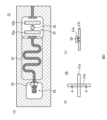
- FIGS. 3(a) to 3(d) are exploded plan views of the printed circuit board 10 in the first embodiment.
- FIG. 4(a) is a cross-sectional view of the printed circuit board 10 at a location corresponding to A-A in FIG. 3(a)
- FIG. 4(b) is a cross-sectional view of the printed circuit board 10 at a location corresponding to B-B in FIG. 3(a).
- FIGS. 3(a) to 3(d) are plan views of each layer as viewed from above.
- the signal wiring 13, ground wiring 14a, 14b, and 14c, signal via 16, ground via 17, and land 18 are hatched for clarity.
- the printed circuit board 10 includes a signal wiring 13, a plurality of ground wirings 14a, 14b, and 14c, and a plurality of insulating layers 15a, 15b, and 15c.
- the ground wiring 14a third wiring is exposed on the upper surface 11 (first surface) of the printed circuit board 10.
- the ground wiring 14c second wiring is exposed on the lower surface 12 (second surface) of the printed circuit board 10.
- the signal wiring 13 (first wiring) and the ground wiring 14b (fourth wiring) are provided inside the printed circuit board 10. At least a portion of the signal wiring 13 overlaps both the ground wirings 14a and 14c in a plan view.
- the insulating layer 15a is a layer located between the ground wiring 14a and the ground wiring 14b.
- the insulating layer 15b is a layer located between the ground wiring 14b and the signal wiring 13.
- the insulating layer 15c is a layer located between the signal wiring 13 and the ground wiring 14c.
- the signal wiring 13 faces the ground wiring 14b at its top via the insulating layer 15b, and faces the ground wiring 14c at its bottom via the insulating layer 15c, and is sandwiched between the ground wiring 14b and the ground wiring 14c. As a result, the signal wiring 13 and the ground wirings 14b and 14c form a strip line 19.
- the printed circuit board 10 further includes a signal via 16 connected to the signal wiring 13, a ground via 17 connected to the ground wiring 14a, 14b, and 14c, and a land 18 connected to the signal via 16.
- the land 18 is exposed on the top surface 11 of the printed circuit board 10.
- the signal via 16 is provided on the printed circuit board 10 from the land 18 to the signal wiring 13.
- the ground via 17 is provided penetrating from the top surface 11 to the bottom surface 12 of the printed circuit board 10.
- the signal wiring 13 is made of a superconducting material.
- a superconducting material is a material that becomes superconducting at extremely low temperatures (e.g., several tens of mK).
- Examples of superconducting materials used for the signal wiring 13 include aluminum (Al), titanium nitride (TiN), and niobium (Nb).
- No magnetic material is added to the superconducting material of the signal wiring 13.
- the ground wiring 14a, 14b, and 14c are made of a normal conducting material.
- a normal conducting material is a material that does not become superconducting at extremely low temperatures (e.g., several tens of mK). Examples of normal conducting materials used for the ground wiring 14a, 14b, and 14c include copper (Cu) and silver (Ag).
- the insulating layers 15a, 15b, and 15c are formed of, for example, epoxy resin, phenolic resin, or glass epoxy resin.
- the signal vias 16 and lands 18 are formed of a superconducting material (e.g., Al, TiN, Nb) or a normal conducting material (e.g., Cu, Ag).
- the ground vias 17 are formed of a normal conducting material (e.g., Cu, Ag).
- the width W of the signal wiring 13 is several tens of ⁇ m to a hundred and several tens of ⁇ m, for example, 50 ⁇ m to 150 ⁇ m.
- the length L of the signal wiring 13 is several centimeters to several tens of cm, for example, 5 cm to 20 cm.
- the thickness of the signal wiring 13 and the ground wiring 14a, 14b, 14c is several tens of ⁇ m, for example, 10 ⁇ m to 50 ⁇ m.
- the thickness of the insulating layers 15a, 15b, 15c is several tens of ⁇ m to a hundred and several tens of ⁇ m, for example, 80 ⁇ m to 120 ⁇ m.
- the thickness of the conductor on the inner wall of the ground via 17 is, for example, about 25 ⁇ m, and the diameter D1 of the through hole inside the ground via 17 is, for example, about 100 ⁇ m.
- the diameter D2 of the land 18 is, for example, about 400 ⁇ m.
- the distance I between the land 18 and the ground wiring 14a is, for example, about 100 ⁇ m.
- the ground wirings 14a, 14b, and 14c are formed, for example, by attaching a conductive foil of a normal conductive material (e.g., Cu foil) to the surface of the insulating layers 70a and 70b and patterning the conductive foil.
- the signal wiring 13 is formed, for example, by attaching a conductive foil of a superconducting material (e.g., Al foil) to the surface of the insulating layer 70b and patterning the conductive foil.
- the insulating layers 70a and 70b are arranged so as to sandwich a semi-cured insulating layer 71a between them.
- the insulating layer 71a is made of a thermosetting resin (e.g., glass epoxy resin) in a semi-cured state, and serves as an adhesive.
- the semi-cured state means that the curing process has been stopped halfway.
- the cured resin is also called a core, and the semi-cured resin is also called a prepreg.
- the signal wiring 13 faces the ground wiring 14c with the insulating layer 15c sandwiched between them.
- the ground wiring 14b faces the signal wiring 13 with the insulating layer 15b sandwiched between them, and the signal wiring 13 is sandwiched between the ground wiring 14c and itself.
- FIG. 9 is a cross-sectional view showing the cooling structure of the quantum device 100 according to the first embodiment.
- the printed circuit board 10 is shown as a combination of FIG. 4(a) and FIG. 4(b).
- the printed circuit board 10 is placed on the upper surface of the cooling plate 66.
- the ground wiring 14c exposed on the lower surface 12 of the printed circuit board 10 comes into contact with the cooling plate 66.
- the cooling plate 66 is, for example, a copper plate having a thickness of about 1 cm.
- the cooling plate 66 is cooled by a refrigerator (not shown) capable of cooling to about 10 mK, for example.
- the signal wiring 13 is made of a superconducting material, but the ground wiring 14a, 14b, 14c and the ground via 17 are made of a normal conducting material.
- the ground wiring 14a, 14b, 14c and the ground via 17 are cooled to an extremely low temperature, their thermal resistance is kept low compared to when they are made of a superconducting material. This makes it possible to cool the quantum chip 50 to an extremely low temperature.
- the signal wiring 13 is cooled to an extremely low temperature and its electrical resistance is reduced, so that the loss of high frequency signals can be reduced as shown in FIG. 8.
- [Modification] 10(a) and 10(b) are cross-sectional views of a printed circuit board 10a in a modified example of the first embodiment.
- the ground wiring 14c, the insulating layer 15c, the ground wiring 14b, the insulating layer 15b, the signal wiring 13, the insulating layer 15a, and the ground wiring 14a are laminated in this order from the lower surface 12 to the upper surface 11.
- the signal wiring 13 faces the ground wiring 14a at the upper surface via the insulating layer 15a, faces the ground wiring 14b at the lower surface via the insulating layer 15b, and is sandwiched between the ground wiring 14a and the ground wiring 14b. Therefore, a strip line 19 is formed by the signal wiring 13 and the ground wirings 14a and 14b.
- the other configurations are the same as those in the first embodiment, so a description thereof will be omitted.
- the signal wiring 13 is made of a superconducting material. This makes it possible to reduce the loss of high-frequency signals. Also, as shown in FIG. 4(b) and FIG. 10(b), the ground wiring 14a exposed on the upper surface 11 of the printed circuit board 10, 10a and the ground wiring 14c exposed on the lower surface 12 are connected by a ground via 17. The ground wiring 14a, 14c and the ground via 17 are made of a normal conductive material. As a result, as described in FIG.
- the signal wiring 13 faces one of the ground wirings 14a, 14c and the ground wiring 14b, and is sandwiched between them.
- the signal via 16 connected to the signal wiring 13 is formed of a superconducting material or a normal conducting material.
- the signal via 16 is formed of a superconducting material, the loss of high frequency signals can be further reduced.
- the signal via 16 is formed of a normal conducting material, it is possible to form it simultaneously with the ground via 17, thereby reducing manufacturing costs.
- a laminate 72 is formed in which a signal wiring 13 containing a superconducting material and ground wirings 14a, 14b, 14c containing a normal conductive material are laminated with insulating layers 15a, 15b, 15c sandwiched therebetween.
- the ground wiring 14a is exposed on the upper surface 73 of the laminate 72, and the ground wiring 14c is exposed on the lower surface 74.
- a ground via 17 containing a normal conductive material that connects the ground wiring 14a and the ground wiring 14c is formed in the laminate 72. This allows the printed circuit boards 10, 10a to be obtained that can ensure cooling performance even when cooled to extremely low temperatures and reduce high-frequency signal loss.
- the signal wiring 13 faces the ground wiring 14c and the ground wiring 14b, forming a laminate 72 sandwiched between them.
- the signal wiring 13 faces the ground wiring 14a and the ground wiring 14b, forming a laminate 72 sandwiched between them. This forms a strip line 19 that transmits high-frequency signals.
- Example 1 in Example 1 and its modified example, as shown in FIG. 6(a), insulating layer 70c, on which insulating layers 71b, 71c and signal wiring 13 are formed, is sandwiched between conductive foils 77a, 77b, and insulating layer 70c is sandwiched between insulating layers 71b, 71c. Thereafter, as shown in FIG. 6(b), insulating layers 71b, 71c are cured, and then conductive foils 77a, 77b are processed to form ground wiring 14a, 14c, thereby forming laminate 72. This makes it easy to form printed circuit boards 10, 10a.
- FIGS. 11(a) to 11(e) are exploded plan views of the printed circuit board 10b in the second embodiment.
- FIG. 12(a) is a cross-sectional view of the printed circuit board 10b at a location corresponding to A-A in FIG. 11(a)
- FIG. 12(b) is a cross-sectional view of the printed circuit board 10b at a location corresponding to B-B in FIG. 11(a).
- FIGS. 11(a), 11(b), 11(d), and 11(e) are plan views of the layers as viewed from above
- FIG. 11(c) is a plan view of the ground wiring 14b as viewed from below.
- the signal wiring 13 the ground wiring 14a, 14b, and 14c, the signal via 16, the ground via 17, and the land 18 are hatched for clarity.
- the ground wiring 14b includes a first layer 21 and a second layer 22.
- the first layer 21 is provided on the surface 23 of the second layer 22 on the side of the signal wiring 13.
- the first layer 21 is made of a superconducting material, for example, Al.
- the second layer 22 is made of a normal conducting material, for example, Cu.
- the first layer 21 is not provided on the entire surface of the surface 23 of the second layer 22, but is provided on a part of the surface 23 with an area larger than that of the signal wiring 13 so as to overlap the signal wiring 13 in a planar view.
- the first layer 21 has a rectangular shape that is point-symmetrical with respect to a point that overlaps the center point of the signal wiring 13 in a planar view.
- the length L1 from a line that overlaps the center line of the signal wiring 13 in the width direction (Y direction) of the signal wiring 13 to the end of the first layer 21 in the Y direction is three times or more, and may be five times or more, of the width W of the signal wiring 13.
- the length L1 is 500 ⁇ m.
- the length L2 from a point that overlaps the tip of the signal wiring 13 in the length direction (X direction) of the signal wiring 13 to the end of the first layer 21 in the X direction is also three times or more, and may be five times or more, of the width W of the signal wiring 13.
- the first layer 21 is provided on the surface 23 of the second layer 22 from the point where it overlaps with the signal wiring 13 over a range that is at least three times the width W of the signal wiring 13, and may be provided over a range that is at least five times that width.
- ground wiring 14c also has a first layer 24 and a second layer 25.
- the first layer 24 is provided on a surface 26 of the second layer 25 on the signal wiring 13 side.
- the first layer 24 is made of a superconducting material, for example, Al.
- the second layer 25 is made of a normal conducting material, for example, Cu.
- the first layer 24 is not provided on the entire surface 26 of the second layer 25, but is provided on a part of the surface 26 with an area larger than the signal wiring 13 so as to overlap the signal wiring 13 in a planar view.
- the first layer 24, like the first layer 21 of the ground wiring 14b, has a rectangular shape that is point-symmetrical with respect to a point that overlaps the center point of the signal wiring 13 in a planar view.
- the first layer 24, like the first layer 21 of the ground wiring 14b, is provided on the surface 26 of the second layer 25 from the point where it overlaps the signal wiring 13 over a range of three or more times the width W of the signal wiring 13, and may be provided over a range of five or more times the width W of the signal wiring 13.
- Ground via 17 is connected to ground wiring 14a, 14b, and 14c, but in ground wiring 14b and 14c, it is connected to at least second layers 22 and 25.
- the other configurations of the quantum device of Example 2 are the same as those of quantum device 100 of Example 1, so illustrations and descriptions are omitted.
- FIG. 13A is a cross-sectional view showing a first manufacturing method of the printed circuit board 10b in the second embodiment.
- an insulating layer 80a is prepared, in which a ground wiring 14a is formed on the upper surface and a ground wiring 14b having a first layer 21 and a second layer 22 is formed on the lower surface.
- an insulating layer 80b is prepared, in which a signal wiring 13 is formed on the upper surface and a ground wiring 14c having a first layer 24 and a second layer 25 is formed on the lower surface.
- an insulating layer 81a is arranged so as to be sandwiched between the insulating layer 80a and the insulating layer 80b.
- the same process as that shown in FIG. 5B and FIG. 5C in the first embodiment is performed.
- the printed circuit board 10b in the second embodiment is formed.
- FIGS. 14(a) and 14(b) are cross-sectional views showing a first method for forming the two-layered ground wiring 14b in Example 2
- Figures 14(c) to 14(e) are cross-sectional views showing a second method for forming the two-layered ground wiring 14b in Example 2.
- a conductive film 83a (e.g., conductive foil (Cu foil)) made of a normal conductive material is attached to the upper surface of the insulating layer 80a.
- a conductive film 87 which is an integrated film of a superconducting material 85 (e.g., Al film) and a normal conductive material 86 (e.g., Cu film) is attached to the lower surface of the insulating layer 80a.
- the conductive film 87 is formed by forming the film 85 on the surface of the conductive foil film 86 by plating.
- the conductive film 83a on the upper surface of the insulating layer 80a is patterned to form the ground wiring 14a.
- the conductive film 87 on the lower surface of the insulating layer 80a is patterned to form the ground wiring 14b having a two-layer structure of a first layer 21 and a second layer 22.
- conductive films 83b and 83c (e.g., conductive foil (Cu foil)) made of a normal conductive material are attached to the upper and lower surfaces of the insulating layer 80a.
- a film 82 made of a superconducting material e.g., an Al film
- the conductive film 83b on the upper surface of the insulating layer 80a is patterned to form the ground wiring 14a.
- the conductive film 83c on the lower surface of the insulating layer 80a is patterned to form the ground wiring 14b having a two-layer structure of the first layer 21 and the second layer 22.
- the first layer 21 can be formed with good positional accuracy.
- FIG. 13(b) is a cross-sectional view showing a second manufacturing method of the printed circuit board 10b in the second embodiment.
- an insulating layer 80c is prepared in which a ground wiring 14b having a first layer 21 and a second layer 22 is formed on the upper surface and a signal wiring 13 is formed on the lower surface.
- the ground wiring 14b and the signal wiring 13 are formed by a method similar to the first forming method shown in FIG. 14(a) and FIG. 14(b) or the second forming method shown in FIG. 14(c) to FIG. 14(e).
- Insulating layers 81b and 81c are arranged on both sides of the insulating layer 80c, and a conductive film 83a made of a normal conductive material is arranged on the outside of the insulating layer 81b.
- a conductive film 87 in which a film 85 made of a superconducting material and a film 86 made of a normal conductive material are integrated is arranged on the outside of the insulating layer 81c.
- FIG. 15 is a cross-sectional view showing the cooling structure of the quantum device 200 according to the second embodiment.
- the printed circuit board 10b is a combination of FIG. 12(a) and FIG. 12(b).
- the printed circuit board 10b is placed on the upper surface of the cooling plate 66.
- the second layer 25 of the ground wiring 14c exposed on the lower surface 12 of the printed circuit board 10b comes into contact with the cooling plate 66. Since the second layer 25 of the ground wiring 14c, the ground via 17, and the ground wiring 14a are made of normal conductive materials, the thermal resistance is kept low even when cooled to an extremely low temperature.
- [Modification] 16(a) and 16(b) are cross-sectional views of a printed circuit board 10c according to a modification of the second embodiment.
- the ground wiring 14b has the first layer 21 provided on the entire surface of the second layer 22 on the side of the signal wiring 13.
- the ground wiring 14c has the first layer 24 provided on the entire surface of the second layer 25 on the side of the signal wiring 13.
- the other configurations are the same as those in the second embodiment, and therefore will not be described.
- FIGS. 17(a) and 17(b) are cross-sectional views showing a first method for forming a two-layered ground wiring 14b in a modified example of Example 2
- FIGS. 17(c) to 17(e) are cross-sectional views showing a second method for forming a two-layered ground wiring 14b in a modified example of Example 2.
- a conductive film 83a made of a normal conductive material is attached to the upper surface of the insulating layer 80a.
- a conductive film 87 which is an integrated film 85 made of a superconducting material and a film 86 made of a normal conductive material, is attached to the lower surface of the insulating layer 80a.
- the conductive film 87 may be formed by using the film 85 as a conductive foil and plating the film 86 on the entire upper surface, or may be formed by using the film 86 as a conductive foil and plating the film 85 on the entire upper surface.
- the conductive film 83a on the upper surface of the insulating layer 80a is patterned to form the ground wiring 14a.
- the conductive film 87 on the lower surface of the insulating layer 80a is patterned to form the ground wiring 14b, which has a two-layer structure of a first layer 21 and a second layer 22.
- conductive films 83b, 83c of normal conductive material are attached to the upper and lower surfaces of the insulating layer 80a.
- a film 82 made of a superconducting material is formed by plating over the entire surface of the conductive film 83c attached to the lower surface of the insulating layer 80a.
- the conductive film 83b on the upper surface of the insulating layer 80a is patterned to form the ground wiring 14a.
- the film 82 and the conductive film 83c on the lower surface of the insulating layer 80a are patterned to form the ground wiring 14b having a two-layer structure of a first layer 21 and a second layer 22.
- the film 85 made of a superconducting material and the film 86 made of a normal conducting material are switched and attached to the insulating layer of the cured resin.
- a conductive foil made of a superconducting material is used for the conductive film 83c, and a film 82 made of a normal conducting material is formed on the surface of the conductive film 83c by plating.
- the first layer 21 of the ground wiring 14b is provided on the entire surface of the second layer 22 facing the signal wiring 13.
- the first layer 24 of the ground wiring 14c is provided on the entire surface of the second layer 25 facing the signal wiring 13. This makes it easy to form the ground wirings 14b and 14c with a two-layer structure of the first layers 21 and 24 and the second layers 22 and 25.
- a laminate 72 is formed in which the signal wiring 13 faces the ground wiring 14c and the ground wiring 14b and is sandwiched between them (see also FIG. 5(b) and FIG. 6(b)).
- the ground wiring 14b has a first layer 21 and a second layer 22
- the ground wiring 14c has a first layer 24 and a second layer 25.
- the first layers 21 and 24 are made of a superconducting material and are provided facing the signal wiring 13.
- the second layers 22 and 25 are made of a normal conducting material and are provided on the opposite side of the signal wiring 13 with respect to the first layers 21 and 24.
- the first layers 21 and 24 made of a superconducting material are present in the electromagnetic field of the strip line 19, so that the loss of high frequency signals can be further reduced.
- Fig. 19 is a diagram showing the current density versus distance from the surface of the conductor.
- the horizontal axis is the distance from the surface of the conductor, and is expressed in units of skin depth d.
- the vertical axis is the current density, and the current density at the surface of the conductor is expressed as 1.
- the current density attenuates at 1/ ed from the surface of the conductor toward the inside.
- the current density attenuates by about 95% relative to the surface of the conductor, at a location 4d away, at a location 98% away, at a location 5d away, and at a location 6d away, at a location 99% away, and at a location 6d away, at a location 99.75% away.
- ⁇ electrical conductivity in formula (1) becomes large; for example, in the case of Cu, at around 10 mK, ⁇ can be about 100 times larger than at room temperature.
- the skin depth d is about 0.21 ⁇ m at 1 GHz and about 0.07 ⁇ m at 10 GHz.
- ⁇ becomes 10,000 times larger than at room temperature.
- the skin depth d becomes about 0.026 ⁇ m at 1 GHz and about 0.008 ⁇ m at 10 GHz.
- 3d is about 0.078 ⁇ m at 1 GHz and about 0.024 ⁇ m at 10 GHz
- 4d is about 0.104 ⁇ m at 1 GHz and about 0.032 ⁇ m at 10 GHz
- 5d is about 0.13 ⁇ m at 1 GHz and about 0.04 ⁇ m at 10 GHz
- 6d is about 0.16 ⁇ m at 1 GHz and about 0.048 ⁇ m at 10 GHz.
- the ground wiring 14b includes a second layer 22 made of Cu and a first layer 21 made of Al provided on a surface 23 of the second layer 22 on the signal wiring 13 side.
- the ground wiring 14c includes a second layer 25 made of Cu and a first layer 24 made of Al provided on a surface 26 of the second layer 25 on the signal wiring 13 side.
- the high-frequency signal transmitted through the strip line 19 penetrates into the signal wiring 13 side area of the ground wirings 14b and 14c. From the viewpoint of reducing loss, it is preferable that most of the high-frequency signal flows through the first layers 21 and 24 made of Al and that almost no signal flows through the second layers 22 and 25 made of Cu. Therefore, in order to prevent the high-frequency signal from penetrating the second layers 22 and 25, it is preferable to set the thickness of the first layers 21 and 24 to 0.01 ⁇ m or more, based on the above consideration of the skin depth d.
- the thickness of the first layers 21, 24 of the ground wirings 14b, 14c is set to 0.01 ⁇ m or more. This allows the loss of high-frequency signals to be further reduced. From the viewpoint of reducing loss, the thickness of the first layers 21, 24 is preferably 0.05 ⁇ m or more, more preferably 0.1 ⁇ m or more, even more preferably 0.5 ⁇ m or more, and even more preferably 1.0 ⁇ m or more. In other words, the thickness of the first layers 21, 24 is preferably three times or more, more preferably four times or more, even more preferably five times or more, and even more preferably six times or more of the skin depth d calculated by the above formula (1).
- the proximity effect occurring at the interface is on the order of 0.1 ⁇ m. Therefore, by setting the thickness of the first layers 21, 24 to 0.5 ⁇ m or more, the influence of the proximity effect can also be suppressed, and it can be said that the electrical characteristics of the high-frequency signal are generally determined by the characteristics of the superconducting material forming the first layers 21, 24.
- the printed circuit board 10d in the third embodiment has ground wiring 34a, 34b, 34c and ground via 37 made of a superconducting material to which a magnetic material has been added, instead of the ground wiring 14a, 14b, 14c and ground via 17 made of a normal conductive material.
- the ground wiring 34a, 34b, 34c and the ground via 37 are aluminum (Al), titanium nitride (TiN), or niobium (Nb) to which at least one of iron (Fe), gadolinium (Gd), nickel (Ni), and cobalt (Co) has been added as a magnetic material.
- the amount of the magnetic material added is extremely small (for example, about 0.01 atm %).
- the other configurations of the quantum device in the third embodiment are the same as those of the quantum device 100 in the first embodiment, and therefore illustration and description thereof will be omitted.
- the ground wiring 34a, 34b, 34c and the ground via 37 are prevented from having an increased thermal resistance when cooling the quantum chip 50 to operate in a superconducting state. Therefore, in the process of cooling the quantum chip 50, the transfer of heat between the quantum chip 50 and the cooling plate 66 is maintained, and the quantum chip 50 can be cooled to an extremely low temperature. In addition, after the quantum chip 50 is cooled to an extremely low temperature, the ground wirings 34a, 34b, and 34c are cooled to the superconducting transition temperature and the ground wirings 34a, 34b, and 34c become superconducting, thereby reducing the loss of high frequency signals.
- W tungsten
- the signal wiring 13 and the ground wiring 34b may be interchanged, as in the modified example of the first embodiment shown in Figs. 10(a) and 10(b).
- the ground wirings 34b and 34c may include a first layer of a superconducting material and a second layer of a superconducting material to which a magnetic material has been added.
- the signal wiring provided on the printed circuit board includes a superconducting material
- the ground wiring and ground vias include a superconducting material with a magnetic material added thereto, but this is not limited to the above.
- the signal wiring provided on the package substrate in FIG. 1 may include a superconducting material
- the ground wiring and ground vias may include a superconducting material with a magnetic material added thereto.
Landscapes
- Engineering & Computer Science (AREA)
- Microelectronics & Electronic Packaging (AREA)
- Superconductor Devices And Manufacturing Methods Thereof (AREA)
Priority Applications (2)
| Application Number | Priority Date | Filing Date | Title |
|---|---|---|---|
| JP2025537301A JPWO2025027675A1 (https=) | 2023-07-28 | 2023-07-28 | |
| PCT/JP2023/027712 WO2025027675A1 (ja) | 2023-07-28 | 2023-07-28 | 量子デバイスおよび多層配線基板の製造方法 |
Applications Claiming Priority (1)
| Application Number | Priority Date | Filing Date | Title |
|---|---|---|---|
| PCT/JP2023/027712 WO2025027675A1 (ja) | 2023-07-28 | 2023-07-28 | 量子デバイスおよび多層配線基板の製造方法 |
Publications (1)
| Publication Number | Publication Date |
|---|---|
| WO2025027675A1 true WO2025027675A1 (ja) | 2025-02-06 |
Family
ID=94394350
Family Applications (1)
| Application Number | Title | Priority Date | Filing Date |
|---|---|---|---|
| PCT/JP2023/027712 Pending WO2025027675A1 (ja) | 2023-07-28 | 2023-07-28 | 量子デバイスおよび多層配線基板の製造方法 |
Country Status (2)
| Country | Link |
|---|---|
| JP (1) | JPWO2025027675A1 (https=) |
| WO (1) | WO2025027675A1 (https=) |
Citations (4)
| Publication number | Priority date | Publication date | Assignee | Title |
|---|---|---|---|---|
| JPH05226901A (ja) | 1992-02-12 | 1993-09-03 | Nippon Telegr & Teleph Corp <Ntt> | 高周波通信系の等化器 |
| JPH10224110A (ja) | 1997-02-12 | 1998-08-21 | Idotai Tsushin Sentan Gijutsu Kenkyusho:Kk | 超伝導平面回路およびその製造方法 |
| JP2020535660A (ja) | 2017-10-31 | 2020-12-03 | ノースロップ グラマン システムズ コーポレイションNorthrop Grumman Systems Corporation | 超伝導電気カプラを備えた熱絶縁グランド面 |
| JP2022002235A (ja) * | 2020-06-19 | 2022-01-06 | 日本電気株式会社 | 量子デバイス |
-
2023
- 2023-07-28 WO PCT/JP2023/027712 patent/WO2025027675A1/ja active Pending
- 2023-07-28 JP JP2025537301A patent/JPWO2025027675A1/ja active Pending
Patent Citations (4)
| Publication number | Priority date | Publication date | Assignee | Title |
|---|---|---|---|---|
| JPH05226901A (ja) | 1992-02-12 | 1993-09-03 | Nippon Telegr & Teleph Corp <Ntt> | 高周波通信系の等化器 |
| JPH10224110A (ja) | 1997-02-12 | 1998-08-21 | Idotai Tsushin Sentan Gijutsu Kenkyusho:Kk | 超伝導平面回路およびその製造方法 |
| JP2020535660A (ja) | 2017-10-31 | 2020-12-03 | ノースロップ グラマン システムズ コーポレイションNorthrop Grumman Systems Corporation | 超伝導電気カプラを備えた熱絶縁グランド面 |
| JP2022002235A (ja) * | 2020-06-19 | 2022-01-06 | 日本電気株式会社 | 量子デバイス |
Non-Patent Citations (1)
| Title |
|---|
| CHARLES KITTEL: "Introduction to Solid State Physics", vol. 10, article "Superconductivity", pages: 278 |
Also Published As
| Publication number | Publication date |
|---|---|
| JPWO2025027675A1 (https=) | 2025-02-06 |
Similar Documents
| Publication | Publication Date | Title |
|---|---|---|
| US11057996B2 (en) | Circuit board, method of manufacturing circuit board, and electronic device | |
| CA2729740C (en) | Embedded rf vertical interconnect for flexible conformal antenna | |
| US10083887B2 (en) | Chip component-embedded resin multilayer substrate and manufacturing method thereof | |
| TWI411073B (zh) | 嵌埋被動元件之封裝基板及其製法 | |
| JP5673673B2 (ja) | 機能素子内蔵基板 | |
| EP3547363B1 (en) | Electronic assembly and electronic system with impedance matched interconnect structures | |
| JPH11317582A (ja) | 多層配線基板およびその製造方法 | |
| US10187971B2 (en) | Wiring board and method of manufacturing wiring board | |
| JP7211540B2 (ja) | 配線基板及びその製造方法 | |
| US12336093B2 (en) | Multilayer board and method of manufacturing the same | |
| US11690173B2 (en) | Circuit board structure | |
| JP6167006B2 (ja) | 導波路基板 | |
| CN218450661U (zh) | 电路板、封装结构及电子设备 | |
| JP2002016327A (ja) | 配線基板およびその製造方法 | |
| JP2010212375A (ja) | Ic搭載基板、プリント配線板、及び製造方法 | |
| US8334590B1 (en) | Semiconductor device having insulating and interconnection layers | |
| JP4462473B2 (ja) | 高周波回路基板及びそれを用いた半導体装置 | |
| US20250096145A1 (en) | Electronic packaging structure | |
| WO2025027675A1 (ja) | 量子デバイスおよび多層配線基板の製造方法 | |
| JP2008182039A (ja) | 多層配線板およびその製造方法 | |
| JP2001345559A (ja) | 配線基板及びその製造方法 | |
| US12557711B2 (en) | Electronic package structure and manufacturing method thereof | |
| CN100553408C (zh) | 具有嵌入式元件的基板及其制造方法 | |
| US11895773B2 (en) | Circuit board structure | |
| CN112020209B (zh) | 印刷电路板及包括印刷电路板的天线模块板 |
Legal Events
| Date | Code | Title | Description |
|---|---|---|---|
| 121 | Ep: the epo has been informed by wipo that ep was designated in this application |
Ref document number: 23947475 Country of ref document: EP Kind code of ref document: A1 |
|
| ENP | Entry into the national phase |
Ref document number: 2025537301 Country of ref document: JP Kind code of ref document: A |
|
| WWE | Wipo information: entry into national phase |
Ref document number: 2023947475 Country of ref document: EP |
|
| NENP | Non-entry into the national phase |
Ref country code: DE |