WO2025013255A1 - 光半導体装置の製造方法及び低反射率膜の設計方法 - Google Patents
光半導体装置の製造方法及び低反射率膜の設計方法 Download PDFInfo
- Publication number
- WO2025013255A1 WO2025013255A1 PCT/JP2023/025764 JP2023025764W WO2025013255A1 WO 2025013255 A1 WO2025013255 A1 WO 2025013255A1 JP 2023025764 W JP2023025764 W JP 2023025764W WO 2025013255 A1 WO2025013255 A1 WO 2025013255A1
- Authority
- WO
- WIPO (PCT)
- Prior art keywords
- coating film
- refractive index
- reflectance
- film
- wavelength
- Prior art date
- Legal status (The legal status is an assumption and is not a legal conclusion. Google has not performed a legal analysis and makes no representation as to the accuracy of the status listed.)
- Pending
Links
Images








Classifications
-
- H—ELECTRICITY
- H01—ELECTRIC ELEMENTS
- H01S—DEVICES USING THE PROCESS OF LIGHT AMPLIFICATION BY STIMULATED EMISSION OF RADIATION [LASER] TO AMPLIFY OR GENERATE LIGHT; DEVICES USING STIMULATED EMISSION OF ELECTROMAGNETIC RADIATION IN WAVE RANGES OTHER THAN OPTICAL
- H01S5/00—Semiconductor lasers
- H01S5/02—Structural details or components not essential to laser action
- H01S5/028—Coatings ; Treatment of the laser facets, e.g. etching, passivation layers or reflecting layers
Definitions
- This disclosure relates to a method for manufacturing an optical semiconductor device and a method for designing a low reflectance film.
- the minimum reflectance R0 at this time is expressed by the following equation (1) and is uniquely determined.
- the minimum reflectance R for the wavelength ⁇ was uniquely determined by the effective refractive index n of the optical semiconductor device and the refractive index n of the coating film provided on the emission end face (front end face) of the optical semiconductor device, and the minimum reflectance R could not be changed.
- the present disclosure has been made to solve the problems described above, and aims to provide a method for manufacturing an optical semiconductor device having a low-reflectance film that is controlled to a desired minimum reflectance at a desired wavelength by replacing a single-layer coating film with a multilayer coating film of three or more layers using a characteristic matrix, and to provide a method for designing a low-reflectance film.
- a method for producing an optical semiconductor device includes: A method for manufacturing an optical semiconductor device having a low reflectance film formed thereon, the low reflectance film having an effective refractive index of n and a desired minimum reflectance R at a desired wavelength ⁇ , comprising the steps of:
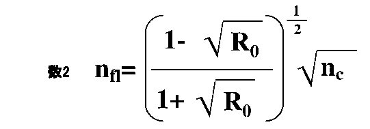
- the refractive index n fl is expressed by the following formula:
- a characteristic matrix of a coating film consisting of a single layer having a film thickness of ⁇ 0 /4/n fl is equal to a characteristic matrix of a multilayer coating film consisting of three or more coating layers using two or more materials in which the refractive index of at least one material is lower than the refractive index n fl and the refractive index of at least one other material is higher than the refractive index n fl , thereby calculating a minimum value R min 0 of the reflectance having wavelength dependency of the reflectance of the multilayer coating film;
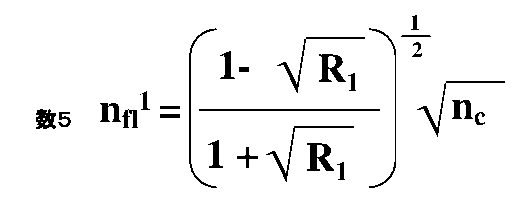
- the refractive index n fl 1 of the coating film made of a single layer that realizes a preset reflectance R 1 is expressed by the following formula:
- the minimum value R min of the reflectance at a wavelength ⁇ min in the wavelength dependence of the reflectance of the multilayer coating film is made to coincide with the minimum reflectance R 0 ;
- a multilayer coating is formed on the end face based on each film thickness of the three or more coating layers obtained by matching the minimum value R min at the wavelength ⁇ min with the minimum reflectance R 0 at the wavelength ⁇ 0 .
- the method for designing a low reflectance film includes the steps of: A method for designing a low reflectance film having a minimum reflectance R 0 , which is a desired minimum reflectance other than zero, on an end face of an optical semiconductor device having an effective refractive index n c , comprising the steps of: Calculating the refractive index n fl by the following formula:
- calculating a minimum value R min 0 of the wavelength-dependent reflectance of the multilayer coating film by equating a characteristic matrix of a coating film consisting of a single layer having a film thickness of ⁇ 0 /4/ n fl at a desired wavelength ⁇ 0 with a characteristic matrix of a multilayer coating film consisting of three or more coating layers using two or more materials, at least one of which has a refractive index lower than the refractive index n fl and at least one of which has a refractive index higher than the refractive index n fl ;
- the manufacturing method of an optical semiconductor device and the design method of a low reflectance film according to the present disclosure make it possible to manufacture an optical semiconductor device having a low reflectance film that is controlled to a desired minimum reflectance at a desired wavelength by replacing a single-layer coating film with a multilayer coating film of three or more layers using a characteristic matrix, and also to obtain a method for designing a low reflectance film.
- FIG. 1 is a schematic diagram of a quantum cascade laser device which is an example of an optical semiconductor device according to a first embodiment
- 2 is a cross-sectional view taken along line AA of FIG. 1 in a quantum cascade laser device which is an example of an optical semiconductor device in the first embodiment
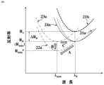
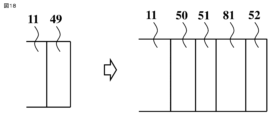
- 4 is a schematic diagram for explaining a method of designing a low-reflectance film having a minimum reflectance of the optical semiconductor device in the first embodiment.
- FIG. 1 is a diagram showing the wavelength dependence of the reflectance of a low-reflectance film designed by the design method for a low-reflectance film having a minimum reflectance of an optical semiconductor device in accordance with the first embodiment.
- FIG. 1 is a diagram showing the wavelength dependence of the reflectance of a low-reflectance film designed by the design method for a low-reflectance film having a minimum reflectance of an optical semiconductor device in accordance with the first embodiment.
- FIG. 3 is a schematic diagram showing a method for designing a low-reflectance film having a minimum reflectance of the optical semiconductor device in the first embodiment.
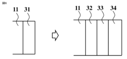
- FIG. 4 is a schematic diagram for explaining a method of designing a low-reflectance film having a minimum reflectance of the optical semiconductor device in the first embodiment.
- FIG. 1 is a diagram showing the wavelength dependence of the reflectance of a low-reflectance film designed by the design method for a low-reflectance film having a minimum reflectance of an optical semiconductor device in accordance with the first embodiment.
- FIG. 11 is a schematic diagram for explaining a method of designing a low-reflectance film having a minimum reflectance of an optical semiconductor device in accordance with a second embodiment.
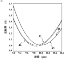
- FIG. 1 is a diagram showing the wavelength dependence of the reflectance of a low-reflectance film designed by the design method for a low-reflectance film having a minimum reflectance of an optical semiconductor device in accordance with the first embodiment.
- FIG. 11 is a schematic diagram for explaining
- FIG. 13 is a diagram showing the wavelength dependence of the reflectance of a low-reflectance film designed by a design method for a low-reflectance film having a minimum reflectance of an optical semiconductor device in accordance with the second embodiment.
- FIG. 11 is a schematic diagram for explaining a method of designing a low-reflectance film having a minimum reflectance of an optical semiconductor device in accordance with a second embodiment.
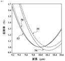
- FIG. 13 is a diagram showing the wavelength dependence of the reflectance of a low-reflectance film designed by a design method for a low-reflectance film having a minimum reflectance of an optical semiconductor device in accordance with the second embodiment.
- FIG. 11 is a schematic diagram for explaining a method of designing a low-reflectance film having a minimum reflectance of an optical semiconductor device in accordance with a second embodiment.
- FIG. 13 is a diagram showing the wavelength dependence of the reflectance of a low-reflectance film designed by a design method for a low-reflectance film having a minimum reflect
- FIG. 13 is a schematic diagram for explaining a method of designing a low-reflectance film having a minimum reflectance of an optical semiconductor device in the third embodiment.
- FIG. 13 is a diagram showing the wavelength dependence of the reflectance of a low-reflectance film designed by a design method for a low-reflectance film having a minimum reflectance of an optical semiconductor device in accordance with the third embodiment.
- FIG. 13 is a schematic diagram for explaining a method of designing a low-reflectance film having a minimum reflectance of an optical semiconductor device in the third embodiment.
- FIG. 13 is a diagram showing the wavelength dependence of the reflectance of a low-reflectance film designed by a design method for a low-reflectance film having a minimum reflectance of an optical semiconductor device in accordance with the third embodiment.
- FIG. 13 is a schematic diagram for explaining a method of designing a low-reflectance film having a minimum reflectance of an optical semiconductor device in accordance with a fourth embodiment.
- FIG. 13 is a diagram showing the wavelength dependence of the reflectance of a low-reflectance film designed by a design method for a low-reflectance film having a minimum reflectance of an optical semiconductor device in accordance with the fourth embodiment.
- FIG. 13 is a schematic diagram for explaining a method of designing a low-reflectance film having a minimum reflectance of an optical semiconductor device in accordance with a fourth embodiment.
- FIG. 13 is a diagram showing the wavelength dependence of the reflectance of a low-reflectance film designed by a design method for a low-reflectance film having a minimum reflectance of an optical semiconductor device in accordance with the fourth embodiment.
- FIG. 13 is a diagram showing the wavelength dependence of the reflectance of a low-reflectance film designed by a design method for a low-reflectance film having a minimum reflect
- Embodiment 1. 1 is a schematic diagram showing a quantum cascade laser device 100 which is an example of an optical semiconductor device according to the first embodiment.
- the quantum cascade laser device 100 according to the first embodiment includes an n-type first electrode 1, an n-type InP substrate 2, an n-type InP buffer layer 3, an n-type GaInAs first optical confinement layer 4, a core region 5 consisting of 30 to 40 stages, an n-type GaInAs second optical confinement layer 6, an n-type InP cladding layer 7, an n-type GaInAs contact layer 8, and an n-type second electrode 9.
- the quantum cascade laser device 100 may be referred to as an optical semiconductor device 11.
- the first stage of the core region 5 has a multi-quantum well (MQW) structure in which many GaInAs well layers and AlInAs barrier layers are stacked, and the oscillation wavelength is mid-infrared light in the range of 3 to 24 ⁇ m. Note that the low-reflectance film 10 provided on the front end face is not shown in Figure 1.
- MQW multi-quantum well
- Fig. 2 is a cross-sectional view of the quantum cascade laser device 100 taken along line A-A in Fig. 1.
- the emission end face of the quantum cascade laser device 100 is provided with a low reflectance film 10 which is made up of a plurality of coating films (hereinafter referred to as a multilayer coating film) and has a minimum reflectance at a wavelength ⁇ 0 .
- a single-layer coating film (hereinafter referred to as a single-layer coating film) having a refractive index of nf at a wavelength ⁇ 0 and a film thickness set to ⁇ 0 /( 4nf ) is provided on optical semiconductor device 11 having an effective refractive index of nc, the reflectance of the single-layer coating film becomes a minimum reflectance R0, which is a minimum value.
- the minimum reflectance R0 is expressed by the above-mentioned formula (1).
- the refractive index n fl and the refractive index n fh of the coating film for realizing the desired minimum reflectance R 0 are calculated using the following equation (2).
- the refractive indexes n fl and n fh are calculated to be 1.666535 and 1.920152, respectively.
- the above-mentioned refractive index values are realized by substituting known materials.
- FIG. 3 is a schematic diagram of a case where a single-layer coating film 12 having a refractive index n fl and a thickness d fl of ⁇ 0 /(4n fl ) is replaced with a three-layer coating film having a refractive index n 1 and a thickness d 1 , a refractive index n 2 and a thickness d 2 , and a refractive index n 1 and a thickness d 3 . As shown in FIG.
- the characteristic matrices of both become equal as expressed by the following formula (3).
- phase terms ⁇ 1 , ⁇ 2 and ⁇ 3 of the coating films in formula (3) are expressed by the following formula (4).
- Equation (3) the refractive indexes n 1 and n 2 are known, so there are three unknowns: film thicknesses d 1 , d 2 , and d 3 . Each film thickness can be calculated by solving equation (3).
- the wavelength dependency of the reflectance in this case is shown by the dashed line 22 in FIG. 4.
- the reflectance is 0.5% at a wavelength of 10 ⁇ m, but this value is not a minimum value, and the minimum value R min 0 of the reflectance of the three-layer coating film is 0.4857%.
- R min and R min 0 are as follows. (1) R min : the minimum value of the reflectance of the multilayer coating film when the set reflectance R 1 of the single-layer coating film is replaced by the multilayer coating film. (2) R min 0 : the minimum value of the reflectance of the multilayer coating film when the desired minimum reflectance R 0 of the single-layer coating film is replaced by the multilayer coating film.
- the minimum reflectance R 0 of the single-layer coating film is 0.5%, whereas the minimum value R min 0 of the reflectance of the triple-layer coating film is 0.4857%, which is lower than the minimum reflectance R 0 of the single-layer coating film. Therefore, the set reflectance R 1 is set high so that the minimum value R min of the reflectance of the triple-layer coating film becomes the desired minimum reflectance R 0.
- the increment ⁇ R 0 is 0.0146%
- the wavelength dependency of the reflectance in this case is shown by the two-dot chain line 23 in Fig. 4.
- the wavelength ⁇ min at which the minimum reflectance is achieved is set to the desired wavelength ⁇ 0.
- the dashed line 21 in Fig. 4 represents the wavelength dependence of reflectance for a single-layer coating having a refractive index of n fl and a thickness of ⁇ 0 /(4n fl ).
- the solid line 24 and dashed line 21 in Fig. 4 do not completely match, but they show almost the same wavelength dependence of reflectance, and the minimum reflectance and the wavelength at which the minimum reflectance is obtained are completely matched.
- YF 3 is used for the first coating film 13 and the third coating film 15, and ZnS is used for the second coating film 14, but the present invention is not limited thereto, and it is sufficient that there is one or more materials whose refractive indexes are higher than n fl and n fl 1 and one or more materials whose refractive indexes are lower than n fl and n fl 1 , and the order of each material can be selected arbitrarily. From the above, it can be seen that a desired minimum reflectance at a desired wavelength can be achieved by using a material with a known refractive index.
- FIG. 5 is a schematic diagram showing a method of replacing a single-layer coating having a refractive index n fl and a thickness ⁇ 0 /(4n fl ) with a three-layer coating, which has a minimum reflectance R 0 at a wavelength ⁇ 0.
- the dotted line 21a represents the wavelength dependence of the reflectance of a single-layer coating having a refractive index n fl and a thickness ⁇ 0 /(4n fl ), and indicates the minimum reflectance R 0 at a wavelength ⁇ 0 .
- the thicknesses of the three-layer coating are determined so that the characteristic matrices of the two are equal.
- the minimum reflectance R 0 is obtained at wavelength ⁇ 0
- the minimum reflectance value of the three-layer coating (minimum value R min 0 of the reflectance of the three-layer coating) and the wavelength ( ⁇ min ) at which the minimum reflectance is obtained are different.
- the wavelength dependency of the reflectance in this case is represented by the dashed line 22a in FIG. 5.
- the minimum reflectance R1 of the single-layer coating film is set as R0 + ⁇ R0 so that the minimum value Rmin of the reflectance of the three-layer coating film coincides with the desired minimum reflectance R0 .
- the wavelength dependency of the reflectance in this case is represented by the two-dot chain line 23a in Figure 5.
- each of the three coating layers is multiplied by ⁇ 0 / ⁇ min so as to obtain a minimum reflectance R 0 at a wavelength ⁇ 0.
- the wavelength dependency of the reflectance in this case is represented by a solid line 24a in FIG.
- the method of replacing the single-layer coating film with a three-layer coating film is the
- the wavelength dependency of the reflectance in this case is shown by the two-dot chain line 37 in Fig. 7.
- the wavelength ⁇ min at which the minimum reflectance is achieved is set to the desired wavelength ⁇ 0 .
- d 1 423.150 nm
- d 2 543.247 nm
- d 3 423.150 nm
- the dashed line 35 in Fig. 7 represents the wavelength dependence of reflectance for a single-layer coating having a refractive index of nfh and a thickness of ⁇ 0 /( 4nfh ).
- the solid line 38 and dashed line 35 in Fig. 7 do not completely match, but they show almost the same wavelength dependence of reflectance, and the minimum reflectance and the wavelength at which the minimum reflectance is obtained are completely matched.
- YF3 is used for the first coating film 32 and the third coating film 34
- ZnS is used for the second coating film 33, but the present invention is not limited thereto, and it is sufficient that there is one or more materials whose refractive indexes are higher than nfh and nfh1 and one or more materials whose refractive indexes are lower than nfh and nfh1 , and the order of the materials can be selected arbitrarily. From the above, it can be seen that a desired minimum reflectance at a desired wavelength can be achieved with a material having a known refractive index.
- the above-mentioned method for manufacturing an optical semiconductor device utilizes the concept of the above-mentioned design method for the low-reflectance film, and it does not matter if the individual coating films of the multilayer coating film do not match exactly during manufacturing.
- the manufacturing method for a low-reflectance film designed by the following method and provided on an optical semiconductor device is included in the present disclosure.
- a single-layer coating film having the desired minimum reflectance ( R0 ) is replaced with a multilayer coating film, and the minimum value ( Rmin0 ) of the reflectance of the multilayer coating film and the wavelength ( ⁇ min ) at which the minimum reflectance is obtained are calculated.
- the minimum reflectance R1 of the single-layer coating film is set to R0 + ⁇ R0 so that the minimum value ( Rmin ) of the reflectance of the multilayer coating film coincides with the desired minimum reflectance ( R0 ).
- each film thickness of the multilayer coating film is calculated so that the desired minimum reflectance ( R0 ) is obtained at the desired wavelength ( ⁇ 0 ).
- Embodiment 2 The minimum reflectance R 0 can be set to a desired value.
- an example of the minimum reflectance R 0 0.01 (1%) is shown. If the effective refractive index n c of the optical semiconductor device is 3.2, then n fl and n fh are calculated to be 1.618080 and 1.977653, respectively, from the above formula (2).
- FIG. 8 is a schematic diagram of a case where a single-layer coating film 41 having a refractive index n fl and a thickness d fl of ⁇ 0 /(4n fl ) is replaced with a three-layer coating film having a refractive index n 1 and a thickness d 1 , a refractive index n 2 and a thickness d 2 , and a refractive index n 3 and a thickness d 3 . As shown in FIG.
- the characteristic matrices of both become equal as expressed by the following formula (10).
- phase terms ⁇ 1 , ⁇ 2 and ⁇ 3 of each coating film are expressed as the following formula (11).
- equation (10) the refractive indexes n1 , n2, and n3 are known, so there are three unknowns: film thicknesses d1 , d2 , and d3 .
- the film thickness of each coating film can be calculated.
- the wavelength dependency of the reflectance in this case is shown by the dashed line 46 in FIG. 9.
- the reflectance is 1.0% at a wavelength of 10 ⁇ m, but this value is not a minimum value, and the minimum value R min 0 of the reflectance of the three-layer coating film is 0.9836%.
- the minimum reflectance R0 of the single-layer coating film is 1.0%, while the minimum value Rmin0 of the reflectance of the three-layer coating film is 0.9836%, which is lower than the minimum reflectance R0 of the single-layer coating film. Therefore, similar to the first embodiment, the set reflectance R1 is set high at 1.01648% in order to make the minimum value Rmin of the reflectance of the three-layer coating film the desired minimum reflectance R0 .
- nfl1 is calculated as 1.616739 from the formula (5).
- the thicknesses of the coating films are calculated by solving the following formula (12), and d1 is calculated as 641.123 nm, d2 is calculated as 205.474 nm, and d3 is calculated as 765.332 nm.
- the wavelength dependency of the reflectance in this case is shown by the two-dot chain line 47 in Fig. 9.
- the wavelength ⁇ min at which the minimum reflectance is obtained is set to the desired wavelength ⁇ 0.
- d 1 649.962 nm
- d 2 208.307 nm
- the dashed line 45 in FIG. 9 shows the wavelength dependency of the reflectance for a single-layer coating film with a refractive index of n fl and a film thickness of ⁇ 0 /(4n fl ).
- the solid line 48 and dashed line 45 in FIG. 9 show almost the same wavelength dependency of the reflectance, and the minimum reflectance and the wavelength at which the minimum reflectance is obtained are completely the same.
- YF 3 is used for the first coating film 42
- ZnS is used for the second coating film 43
- CeF 3 is used for the third coating film 44
- the present invention is not limited to these, and it is sufficient to have one or more materials with refractive indices higher than n fl and n fl 1 and one or more materials with refractive indices lower than n fl and n fl 1 , and the order of each material can be selected arbitrarily. From the above, it can be seen that a desired minimum reflectance at a desired wavelength can be achieved by using a material with a known refractive index.
- n fh 1.977653.
- the wavelength dependency of the reflectance in this case is shown by the dashed line 54 in FIG. 11.
- the reflectance is 1.0% at a wavelength of 10 ⁇ m, but this value is not a minimum value, and the minimum value R min 0 of the reflectance of the three-layer coating film is 0.94561%.
- the minimum reflectance R 0 of the single-layer coating film is 1.0%, while the minimum value R min 0 of the reflectance of the three-layer coating film is 0.94561%, which is lower than the minimum reflectance R 0 of the single-layer coating film. Therefore, similar to the first embodiment, in order to make the minimum value R min of the reflectance of the three-layer coating film the desired minimum reflectance R 0 , the set reflectance R 1 is set high to 1.057485%.
- the wavelength dependency of the reflectance in this case is shown by the two-dot chain line 55 in Fig. 11.
- the wavelength ⁇ min at which the minimum reflectance is achieved is set to the desired wavelength ⁇ 0.
- the wavelength dependency of reflectance in this case is shown by the solid line 56 in Figure 11. It can be seen that the minimum reflectance is 1.0% at the wavelength ⁇ 0 .
- the dashed line 53 in Fig. 11 represents the wavelength dependence of reflectance for a single-layer coating having a refractive index of nfh and a thickness of ⁇ 0 /( 4nfh ).
- the solid line 56 and dashed line 53 in Fig. 11 do not perfectly match, but they show almost the same wavelength dependence of reflectance, and the minimum reflectance and the wavelength at which the minimum reflectance is obtained are completely matched.
- YF 3 is used for the first coating film 50
- ZnS is used for the second coating film 51
- CeF 3 is used for the third coating film 52
- the present invention is not limited to these, and it is sufficient that there is one or more materials whose refractive index is higher than n fh and n fh 1 , and one or more materials whose refractive index is lower than n fh and n fh 1 , and the order of each material can be selected arbitrarily. From the above, it can be seen that a desired minimum reflectance at a desired wavelength can be achieved by using a material with a known refractive index.
- the above-mentioned method for manufacturing an optical semiconductor device utilizes the concept of the above-mentioned design method for the low-reflectance film, and it does not matter if the individual coating films of the multilayer coating film do not match exactly during manufacturing.
- the method for manufacturing a low-reflectance film designed according to the design method of embodiment 2 and provided on an optical semiconductor device is included in the present disclosure.
- Embodiment 3 a method for realizing a desired minimum reflectance at a desired wavelength by using four or more materials with different refractive indices will be described.
- a multi-layer coating film made of four or more materials a five-layer coating film will be described.
- the minimum reflectance R 0 0.01 (1%) is taken as an example. If the effective refractive index n c of the optical semiconductor device is 3.2, the refractive indexes n fl and n fh are calculated to be 1.618080 and 1.977653, respectively, from equation (2).
- FIG. 12 is a schematic diagram of a case where a single-layer coating film 41 having a refractive index n fl and a thickness d fl of ⁇ 0 /(4n fl ) is replaced with a five- layer coating film having a refractive index n 1 and a thickness d 1 , a refractive index n 2 and a thickness d 2 , a refractive index n 3 and a thickness d 3 , a refractive index n 4 and a thickness d 4 , and a refractive index n 5 and a thickness d 5 .
- the single-layer coating film 41 having a refractive index n fl and a thickness d fl of ⁇ 0 /(4n fl ) formed on an end face of an optical semiconductor device 11 emitting light of a wavelength ⁇ 0 with an effective refractive index n c is replaced with a five-layer coating film including a first coating film 61 having a refractive index n 1 and a thickness d 1 , a second coating film 62 having a refractive index n 2 and a thickness d 2 , a third coating film 63 having a refractive index n 3 and a thickness d 3 , a fourth coating film 64 having a refractive index n 4 and a thickness d 4 , and a fifth coating film 65 having a refractive index n 5 and a thickness d 5 .
- the characteristic matrices of the two become equal, as expressed by
- phase terms ⁇ 1 , ⁇ 2 , ⁇ 3 , ⁇ 4 and ⁇ 5 of each coating film in equation (15) are expressed by the following equation (16).
- the film thicknesses of two of the five materials are set to preset film thicknesses.
- the film thicknesses d1 and d2 of the first coating film 61 and the second coating film 62 are set to preset film thicknesses.
- the film thicknesses of the coating films are d 3
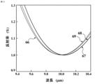
- the wavelength dependency of the reflectance in this case is shown by the dashed dotted line 67 in Fig. 13.
- the reflectance is 1.0% at a wavelength of 10 ⁇ m, but this value is not a minimum value, and the minimum value R min 0 of the reflectance of the five-layer coating film is 0.998474%.
- the wavelength dependency of the reflectance in this case is shown by the two-dot chain line 68 in Fig. 13.
- the wavelength ⁇ min at which the reflectance becomes minimum is set to the desired wavelength ⁇ 0 .
- the first coating film 61 and the second coating film 62 are also multiplied by ⁇ 0 / ⁇ min .
- the dashed line 66 in Fig. 13 represents the wavelength dependence of reflectance for a single-layer coating having a refractive index of n fl and a thickness of ⁇ 0 /(4n fl ).
- the solid line 69 and dashed line 66 in Fig. 13 do not completely match, but they show almost the same wavelength dependence of reflectance, and the minimum reflectance and the wavelength at which the minimum reflectance is obtained are completely matched.
- CeO 2 is used for the first coating film 61, ZnS for the second coating film 62, YF 3 for the third coating film 63, ZnSe for the fourth coating film 64, and CeF 3 for the fifth coating film 65, but the present invention is not limited to these, and it is sufficient that there is one or more materials whose refractive index is higher than n fl and n fl 1 and one or more materials whose refractive index is lower than n fl and n fl 1 , and the order of each material can be selected arbitrarily.
- the two coating films with preset thicknesses can also be arbitrarily selected from the five-layer coating film.
- a five-layer coating film was given as an example of a coating film with four or more layers, but by doing the same, it is possible to achieve the desired minimum reflectance at the desired wavelength even with a multi-layer coating film.
- Figure 14 is a schematic diagram of a single-layer coating film 49 having a refractive index nfh and a film thickness dfh of ⁇ 0 /( 4nfh ), being replaced with a five- layer coating film having a refractive index n1 and a film thickness d1, a refractive index n2 and a film thickness d2 , a refractive index n3 and a film thickness d3 , a refractive index n4 and a film thickness d4 , and a refractive index n5 and a film thickness d5.
- the method of replacing the single-layer coating film with the five-layer coating film is the same as that of the low refractive index film described above, and
- the film thicknesses of the coating films are d 3
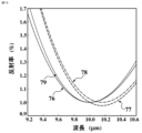
- the wavelength dependency of the reflectance in this case is shown by the dashed-dotted line 77 in Fig. 15.
- the reflectance is 1.0% at a wavelength of 10 ⁇ m, but this value is not a minimum value, and the minimum value R min 0 of the reflectance of the five-layer coating is 0.975517%.
- the minimum reflectance R0 of the single-layer coating film is 1.0%, while the minimum value Rmin0 of the five-layer coating film is 0.975517%, which is lower than the minimum reflectance R0 of the single-layer coating film. Therefore, in order to make the minimum value Rmin of the five-layer coating film the desired minimum reflectance R0 , the set reflectance R1 is set high at 1.025357%.
- the wavelength dependency of reflectance in this case is shown by the two-dot chain line 78 in Fig. 15.
- the wavelength ⁇ min at which the reflectance becomes minimum is set to the desired wavelength ⁇ 0 .
- the first coating film 71 and the second coating film 72 are also multiplied by ⁇ 0 / ⁇ min .
- the dashed line 76 in Fig. 15 represents the wavelength dependence of reflectance for the single-layer coating 49 having a refractive index of nfh and a film thickness of ⁇ 0 /( 4nfh ).
- the solid line 79 and dashed line 76 in Fig. 15 do not perfectly match, but they show almost the same wavelength dependence of reflectance, and the minimum reflectance and the wavelength at which the minimum reflectance is obtained are completely consistent.
- CeO 2 is used for the first coating film 71, ZnS for the second coating film 72, YF 3 for the third coating film 73, ZnSe for the fourth coating film 74, and CeF 3 for the fifth coating film 75
- the present invention is not limited to these, and it is sufficient that there is one or more materials whose refractive index is higher than n fh and n fh 1 and one or more materials whose refractive index is lower than n fh and n fh 1 , and the order of each material can be selected arbitrarily.
- the two coating films with preset thicknesses can also be arbitrarily selected from the five-layer coating film.
- a five-layer coating film was given as an example of a coating film with four or more layers, but by doing the same, it is possible to achieve the desired minimum reflectance at the desired wavelength even with a multi-layer coating film.
- the above-mentioned method for manufacturing an optical semiconductor device utilizes the concept of the above-mentioned design method for the low-reflectance film, and it does not matter if the individual coating films of the multilayer coating film do not match exactly during manufacturing.
- the manufacturing method for a low-reflectance film designed according to the following design method and provided on an optical semiconductor device is included in the present disclosure.
- the film thickness of the excess number of coating films is set in advance. Then, to obtain a desired minimum reflectance (R 0 ) at a desired wavelength ( ⁇ 0 ), a single-layer coating film with the desired minimum reflectance (R 0 ) is replaced with a multilayer coating film, and the minimum value (R min 0 ) of the reflectance of the multilayer coating film and the wavelength ( ⁇ min ) at which the minimum reflectance is obtained are calculated. Next, the minimum reflectance R 1 of the single-layer coating film is set to R 0 + ⁇ R 0 so that the minimum value (R min ) of the reflectance of the multilayer coating film coincides with the desired minimum reflectance (R 0 ). Furthermore, the thickness of each of the multilayer coating films is calculated so that the desired minimum reflectance (R 0 ) is obtained at the desired wavelength ( ⁇ 0 ).
- Embodiment 4 The mirror loss of an optical semiconductor device is defined by the following equation (20).
- Rf , Rr , and L are the front facet reflectivity, rear facet reflectivity, and cavity length, respectively. In applications requiring a narrow band of mirror losses, it is necessary to narrow the band around the minimum reflectivity.
- Fig. 16 is a schematic diagram showing a method of narrowing the band near the minimum reflectance, taking the minimum reflectance shown in the second embodiment (Fig. 8) as an example.
- the fourth embodiment is characterized in that a coating film 81 having a refractive index n a and a film thickness d a of ⁇ 0 /(2n a ) is provided.
- the other coating films are the same as the coating films shown in Fig. 8 of the second embodiment.
- the characteristic matrix of the four-layer coating film of the fourth embodiment is expressed by the following equation (21).
- Equation (21) the phase terms ⁇ 1 , ⁇ 2 , ⁇ 3 and ⁇ a of each coating film are expressed by the following equation (22), and the film thickness d a of the inserted coating film 81 is expressed by the following equation (23).
- the reflectance of the coating film is expressed by the following equation (24) using matrix components m 11 , m 12 , m 21 , and m 22 .
- An example of the material of the inserted coating film 81 is CeO 2 with a refractive index n a of 1.70.
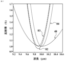
- the wavelength dependency of the reflectance is shown by a dashed line 82 in Fig. 17.
- the minimum value Rmin0 of the reflectance of the four-layer coating film is 0.9609%.
- the refractive index n a of the coating film 81 inserted between the second coating film 43 and the third coating film 44 is 1.70
- the film thickness d a is 2941.176 nm.
- the wavelength dependence of the reflectance of the three-layer coating of the second embodiment is shown by dashed line 48 in Figure 17. It can be seen that the reflectance band is narrow in the vicinity of the desired wavelength ⁇ 0 .
- Fig. 18 is a schematic diagram showing the configuration of the coating film.
- the coating film 81 has a refractive index of n a and a film thickness of d a of ⁇ 0 /(2n a ).
- the other coating films are the same as those in Fig. 10 of the second embodiment.
- the wavelength dependency of the reflectance when the above-mentioned coating film 81 is inserted between the second coating film 51 and the third coating film 52 of the three-layer coating film is shown by the dashed-dotted line 85 in Fig. 19.
- the minimum value Rmin0 of the reflectance of the four-layer coating film is 0.9950%.
- the refractive index n a of the coating film 81 inserted between the second coating film 51 and the third coating film 52 is 1.70
- the film thickness d a is 2941.176 nm.
- the wavelength dependence of the reflectance of the three-layer film of the second embodiment is shown by dashed line 56 in Figure 19. It can be seen that the reflectance band is narrow in the vicinity of the desired wavelength ⁇ 0 .
- a coating film 81 having a desired refractive index n a and a film thickness d a of ⁇ 0 /(2n a ) is inserted, but if the film thickness of the coating film 81 is thicker than ⁇ 0 /(4n a ) and thinner than 3 ⁇ 0 /(4n a ), it is possible to narrow the reflectance band.
- the coating film is inserted to calculate the wavelength dependency of the reflectance, and the minimum value R min 0 of the reflectance of the four-layer coating film is adjusted to the desired minimum reflectance R 0 , and then the desired minimum reflectance R 0 is achieved at the desired wavelength ⁇ 0.
- the above-mentioned method for manufacturing an optical semiconductor device utilizes the concept of the above-mentioned design method for the low-reflectance film, and it does not matter if the individual coating films of the multilayer coating film do not match exactly during manufacturing.
- the manufacturing method for a low-reflectance film designed according to the following design method and provided on an optical semiconductor device is included in the present disclosure.
- the thickness of the coating film to be inserted is set in advance in a range thicker than ⁇ 0 /(4n a ) and thinner than 3 ⁇ 0 /(4n a ). Then, to obtain the desired minimum reflectance (R 0 ) at the desired wavelength ( ⁇ 0 ), the single-layer coating film having the desired minimum reflectance (R 0 ) is replaced with the multilayer coating film, and the minimum value (R min 0 ) of the reflectance of the multilayer coating film and the wavelength ( ⁇ min ) at which the minimum reflectance is obtained are calculated.
- the minimum reflectance R 1 of the single-layer coating film is set to R 0 + ⁇ R 0 so that the minimum value (R min ) of the reflectance of the multilayer coating film coincides with the desired minimum reflectance (R 0 ). Furthermore, the thickness of each layer of the multilayer coating film is calculated so that the desired minimum reflectance (R 0 ) is obtained at the desired wavelength ( ⁇ 0 ).
- the desired minimum reflectance R 0 of 0.5% and 1.0% and the desired wavelength ⁇ 0 of 10 ⁇ m are merely examples and are not limited thereto, and similar design is possible for other desired minimum reflectances and desired wavelengths.
- the minimum reflectance R min 0 of the multilayer coating film when replaced with the multilayer coating film is lower than the minimum reflectance R 0 of the single-layer coating film.
- a desired minimum reflectance can be realized at a desired wavelength in a similar manner.
- this includes modifying, adding, or omitting at least one component, and even extracting at least one component and combining it with a component of another embodiment.
Landscapes
- Physics & Mathematics (AREA)
- Condensed Matter Physics & Semiconductors (AREA)
- General Physics & Mathematics (AREA)
- Electromagnetism (AREA)
- Optics & Photonics (AREA)
- Semiconductor Lasers (AREA)
- Led Devices (AREA)
Abstract
本開示の光半導体装置の製造方法は、膜厚がλ0/4/nflである単層被覆膜(12)の特性行列と、1つの材料の屈折率が屈折率nflよりも低く、他の1つの材料の屈折率が屈折率nflよりも高い2種類以上の材料を用いた多層被覆膜(13、14、15)の特性行列とを等しいとすることにより反射率の極小値Rmin 0を算出し、膜厚がλ0/4/nfl 1の単層被覆膜(12)の特性行列と、1つの材料の屈折率が屈折率nfl 1よりも低く、他の1つの材料の屈折率が屈折率nfl 1よりも高い2種類の材料を用いた多層被覆膜(13、14、15)の特性行列とを等しいとすることにより、多層被覆膜(13、14、15)の波長λminにおける極小値Rminを極小反射率R0と一致させて得られる各膜厚に基づき多層被覆膜(13、14、15)を端面に形成する。
Description
本開示は、光半導体装置の製造方法及び低反射率膜の設計方法に関する。
非特許文献1に開示されているように、波長λ0において実効屈折率nc(=3.6、GaAs)である光半導体装置の出射端面に、屈折率nf(=1.72、Al2O3)の被覆膜を設けると、被覆膜の反射率は膜厚に対して周期的に変化し、膜厚dfがλ0/(4nf)の整数倍の場合に反射率は極小値となる。このときの極小反射率R0は以下の式(1)で表され、一義的に決定される。

例えば半導体レーザ装置においては、しきい値電流低減あるいは効率向上の観点から、半導体レーザ装置の端面反射率と共振器長から算出されるミラー損失を制御する場合、ミラー損失の値を所望の値に変えることができなかった。
I.Ladany et.al.、"Al2O3 half-wave films for long-life cw lasers、"Appl.Phys.Lett.、vol.30、no.2、pp.87-88、1977
従来の光半導体装置の製造方法及び低反射率膜の設計方法では、所望の波長λ0における極小反射率R0を所望の極小反射率に制御することができないという問題があった。
本開示は上記のような問題点を解消するためになされたもので、単層被覆膜を、特性行列を利用して3層以上の多層被覆膜によって置換することにより、所望の波長において所望の極小反射率に制御された低反射率膜を有する光半導体装置の製造方法を得ること、また、低反射率膜の設計方法を得ることを目的とする。
本開示に係る光半導体装置の製造方法は、
実効屈折率がncであり、所望の波長λ0において所望の極小反射率である極小反射率R0となる低反射率膜が形成された光半導体装置の製造方法であって、
屈折率nflが以下の式で表され、
実効屈折率がncであり、所望の波長λ0において所望の極小反射率である極小反射率R0となる低反射率膜が形成された光半導体装置の製造方法であって、
屈折率nflが以下の式で表され、
予め設定された設定反射率R1を実現する単層からなる被覆膜の屈折率nfl 1が、以下の式で表され、

前記波長λminにおける前記極小値Rminを前記波長λ0における前記極小反射率R0と一致させることによって得られる前記3層以上の被覆膜の各膜厚に基づき多層被覆膜を端面に形成する。
本開示に係る低反射率膜の設計方法は、
実効屈折率がncである光半導体装置の端面に、ゼロを除く所望の極小反射率である極小反射率R0を有する低反射率膜の設計方法であって、
屈折率nflが以下の式により、屈折率nflを算出するステップと、
実効屈折率がncである光半導体装置の端面に、ゼロを除く所望の極小反射率である極小反射率R0を有する低反射率膜の設計方法であって、
屈折率nflが以下の式により、屈折率nflを算出するステップと、

予め設定された設定反射率R1を実現する単層からなる被覆膜の屈折率nfl 1を、以下の式を用いて算出するステップと、
前記波長λminにおける前記極小値Rminを前記波長λ0における前記極小反射率R0と一致させることによって得られる前記3層以上の被覆膜の各膜厚に基づき多層被覆膜の各膜厚を決定するステップと、
を備える。
本開示に係る光半導体装置の製造方法及び低反射率膜の設計方法によれば、単層被覆膜を、特性行列を利用して3層以上の多層被覆膜によって置換することにより、所望の波長において所望の極小反射率に制御された低反射率膜を有する光半導体装置を製造することが可能となり、また、低反射率膜の設計方法を得ることが可能となる。
実施の形態1.
図1は、実施の形態1に係る光半導体装置の一例である量子カスケードレーザ装置100を示す概観図である。実施の形態1に係る量子カスケードレーザ装置100は、n型第1電極1と、n型InP基板2と、n型InPバッファ層3と、n型GaInAs第1光閉じ込め層4と、30~40の各ステージ(stage)からなるコア領域5と、n型GaInAs第2光閉じ込め層6と、n型InPクラッド層7と、n型GaInAsコンタクト層8と、n型第2電極9と、を備える。以下、量子カスケードレーザ装置100を、光半導体装置11と呼ぶ場合もある。
図1は、実施の形態1に係る光半導体装置の一例である量子カスケードレーザ装置100を示す概観図である。実施の形態1に係る量子カスケードレーザ装置100は、n型第1電極1と、n型InP基板2と、n型InPバッファ層3と、n型GaInAs第1光閉じ込め層4と、30~40の各ステージ(stage)からなるコア領域5と、n型GaInAs第2光閉じ込め層6と、n型InPクラッド層7と、n型GaInAsコンタクト層8と、n型第2電極9と、を備える。以下、量子カスケードレーザ装置100を、光半導体装置11と呼ぶ場合もある。
コア領域5の1ステージは、GaInAs層のウエル層とAlInAs層のバリア層が多数積層された多重量子井戸(Multi-Quantum Well:MQW)構造であり、発振波長は3~24μmの範囲内の中赤外光である。なお、図1では、前端面に設けた低反射率膜10は図示していない。
図2は、図1のA-A線に沿った量子カスケードレーザ装置100の断面図である。量子カスケードレーザ装置100の出射端面には、複数の被覆膜(以下、多層被覆膜と呼ぶ)で構成され、波長λ0において反射率が極小となる低反射率膜10が設けられている。
実効屈折率がncである光半導体装置11に、波長λ0において屈折率がnfであり、膜厚がλ0/(4nf)に設定された単層の被覆膜(以下、単層被覆膜と呼ぶ)を設けると、単層被覆膜の反射率は極小値である極小反射率R0となる。極小反射率R0は、上述の式(1)で表される。
逆に式(1)より、所望の極小反射率R0を実現するための被覆膜の屈折率nfl、及び屈折率nfhは、以下の式(2)を用いて算出される。

例えば、光半導体装置11の実効屈折率ncが3.2であり、極小反射率R0=0.005(0.5%)である場合、屈折率nfl及び屈折率nfhは、それぞれ、1.666535及び1.920152と算出される。しかしながら、被覆膜を構成する材料において、これらの屈折率値を有し、かつ光半導体装置へ適用可能な材料は現時点では存在しない。そこで、本開示では、既知の材料で置換することによって上述の屈折率値を実現する。
先ず、屈折率nfl=1.666535の場合について説明する。単層被覆膜を、屈折率nflよりも屈折率が低い材料と、屈折率nflよりも屈折率が高い材料の2つの材料による3層被覆膜による置換を考える。
図3は、屈折率nflで膜厚dflがλ0/(4nfl)である単層被覆膜12を、それぞれ屈折率n1で膜厚d1、屈折率n2で膜厚d2及び屈折率n1で膜厚d3である3層被覆膜で置換する場合の模式図である。図3に示すように、実効屈折率ncで波長λ0の光を出射する光半導体装置11の端面に形成された屈折率nfl(=1.66535)で膜厚dfl=λ0/(4nfl)である単層被覆膜12を、屈折率n1で膜厚d1である第1被覆膜13、屈折率n2で膜厚d2である第2被覆膜14、屈折率n1で膜厚d3である第3被覆膜15の3層被覆膜で置き換える。単層被覆膜12を3層被覆膜で置換できるとすると、以下の式(3)で表されるように、両者の特性行列は等しくなる。


式(3)において、屈折率n1及び屈折率n2は既知なので、未知数は、膜厚d1、d2及びd3の3つであり、式(3)を解くことで各膜厚を算出することができる。
波長λ0=10μm、第1被覆膜13及び第3被覆膜15として、屈折率がnflよりも低い屈折率n1=1.40であるYF3を、第2被覆膜14として屈折率がnflよりも高い屈折率n2=2.20であるZnSを一例として式(3)を解くと、各被覆膜の膜厚は、それぞれ、d1=654.371nm、d2=277.806nm、d3=654.371nmとなる。この場合の反射率の波長依存性を図4の一点鎖線22で示す。反射率は波長10μmにおいて0.5%となるが、この値は極小値ではなく、3層被覆膜の反射率の極小値Rmin
0は0.4857%である。
なお、本開示において、RminとRmin 0の意味は、下記のとおりである。
(1)Rmin:単層被覆膜による設定反射率R1を多層被覆膜で置換した場合の多層被覆膜の反射率の極小値
(2)Rmin 0:単層被覆膜による所望の極小反射率R0を多層被覆膜で置換した場合の多層被覆膜の反射率の極小値
なお、本開示において、RminとRmin 0の意味は、下記のとおりである。
(1)Rmin:単層被覆膜による設定反射率R1を多層被覆膜で置換した場合の多層被覆膜の反射率の極小値
(2)Rmin 0:単層被覆膜による所望の極小反射率R0を多層被覆膜で置換した場合の多層被覆膜の反射率の極小値
単層被覆膜の極小反射率R0:0.5%に対して、3層被覆膜の反射率の極小値Rmin
0が0.4857%と、単層被覆膜の極小反射率R0よりも低くなる。そこで、3層被覆膜の反射率の極小値Rminを所望の極小反射率R0にすべく、設定反射率R1を高く設定する。反射率の増分ΔR0の目安を、R0-Rmin
0=0.0143%とし、所望の極小反射率R0と一致するまで増分ΔR0を調整する。実施の形態1では増分ΔR0=0.0146%であり、設定反射率R1は0.51460%となる。以下の式(5)より、設定反射率R1=0.51460%を実現するための単層被覆膜の屈折率nfl
1は、1.6648189と算出される。
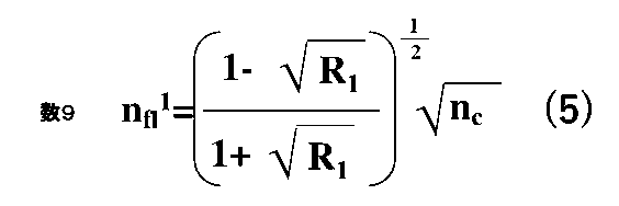
つまり、式(5)より、R1=0.51460%を実現するための単層被覆膜の屈折率nfl
1は1.6648189と算出される。以下の式(6)を解いて各被覆膜の膜厚を計算すると、d1=655.839nm、d2=276.062nm、d3=655.839nmと、それぞれ算出される。

この場合の反射率の波長依存性を図4の二点鎖線23に示す。3層被覆膜の反射率の極小値Rminは、波長λmin=9.876μmにおいて0.5%と、所望の極小反射率である0.5%を得ることができる。
次に、極小反射率となる波長λminを、所望の波長λ0にする。各被覆膜の膜厚をλ0/λmin倍すると、d1=664.074nm、d2=279.528nm、d3=664.074nmと算出される。この場合の反射率の波長依存性を図4の実線24に示す。波長λ0=10μmにおいて極小反射率である0.5%となることが分かる。
なお、図4の破線21は、屈折率nflで膜厚がλ0/(4nfl)である単層被覆膜に関する、反射率の波長依存性である。図4の実線24及び破線21は、完全には一致しないが、ほぼ同一の反射率の波長依存性を示すとともに、極小反射率及び極小反射率となる際の波長は完全に一致する。
極小反射率R0=0.5%及び波長λ0=10μmは例示であり、これらに限るものではなく、所望の数値に設定することができる。また、上述の一例では、第1被覆膜13及び第3被覆膜15にYF3を、第2被覆膜14にZnSをそれぞれ用いたが、これらに限るものではなく、屈折率がnfl及びnfl
1よりも高い材料が1つ以上及び屈折率がnfl及びnfl
1よりも低い材料が1つ以上あれば良く、各材料の順序も任意に選ぶことができる。
以上より、所望の波長において所望の極小反射率を、屈折率が既知の材料を用いて実現できることが分かる。
以上より、所望の波長において所望の極小反射率を、屈折率が既知の材料を用いて実現できることが分かる。
図5は、波長λ0において極小反射率R0である屈折率nflで膜厚がλ0/(4nfl)である単層被覆膜を、3層被覆膜で置換する方法を示す模式図である。図5において、点線21aは屈折率nflで膜厚λ0/(4nfl)である単層被覆膜の反射率の波長依存性を表し、波長λ0において極小反射率R0を示す。
以下に上述の置換方法を説明する。
(1)単層被覆膜(破線21a)を3層被覆膜に置換すべく、両者の特性行列が等しくなるように3層被覆膜の各膜厚を決定する。この場合、波長λ0において極小反射率R0となるが、3層被覆膜の極小反射率の値(3層被覆膜の反射率の極小値Rmin 0)及び極小反射率となる波長(λmin)はずれる。この場合の反射率の波長依存性は、図5の一点鎖線22aで表される。
(2)単層被覆膜の設定反射率R1をR1=R0+ΔR0(破線21b)として特性行列が等しくなる3層被覆膜の各膜厚を算出し、波長λminにおいて極小反射率が所望の3層被覆膜の反射率の極小値Rmin=極小反射率R0となるようにする。つまり、3層被覆膜の反射率の極小値Rminが所望の極小反射率R0と一致するように、単層被覆膜の極小反射率R1をR0+ΔR0と設定する。この場合の反射率の波長依存性は、図5の二点鎖線23aで表される。
(3)波長λ0において極小反射率R0となるように、3層被覆膜の各膜厚をλ0/λmin倍する。この場合の反射率の波長依存性は、図5の実線24aで表される。
(1)単層被覆膜(破線21a)を3層被覆膜に置換すべく、両者の特性行列が等しくなるように3層被覆膜の各膜厚を決定する。この場合、波長λ0において極小反射率R0となるが、3層被覆膜の極小反射率の値(3層被覆膜の反射率の極小値Rmin 0)及び極小反射率となる波長(λmin)はずれる。この場合の反射率の波長依存性は、図5の一点鎖線22aで表される。
(2)単層被覆膜の設定反射率R1をR1=R0+ΔR0(破線21b)として特性行列が等しくなる3層被覆膜の各膜厚を算出し、波長λminにおいて極小反射率が所望の3層被覆膜の反射率の極小値Rmin=極小反射率R0となるようにする。つまり、3層被覆膜の反射率の極小値Rminが所望の極小反射率R0と一致するように、単層被覆膜の極小反射率R1をR0+ΔR0と設定する。この場合の反射率の波長依存性は、図5の二点鎖線23aで表される。
(3)波長λ0において極小反射率R0となるように、3層被覆膜の各膜厚をλ0/λmin倍する。この場合の反射率の波長依存性は、図5の実線24aで表される。
設定反射率R1の設定方法を、以下にさらに詳しく説明する。
最初に置換したときの3層被覆膜の極小反射率が、Rmin 0(0)≠R0となったとすると、このときの所望の反射率R0との差ΔR0 (0)は、ΔR0 (0)=R0-Rmin 0(0)となる。次に、ループ1回目の単層被覆膜の設定反射率R1 (1)を、R1 (1)=R0+ΔR0 (0)とし、3層被覆膜で置換して極小反射率Rmin 0(1)を算出する。算出した結果、Rmin 0(1)=R0であれば、ここで計算を終了する。この場合は、ΔR0=ΔR0 (0)、R1=R1 (1)となる。
最初に置換したときの3層被覆膜の極小反射率が、Rmin 0(0)≠R0となったとすると、このときの所望の反射率R0との差ΔR0 (0)は、ΔR0 (0)=R0-Rmin 0(0)となる。次に、ループ1回目の単層被覆膜の設定反射率R1 (1)を、R1 (1)=R0+ΔR0 (0)とし、3層被覆膜で置換して極小反射率Rmin 0(1)を算出する。算出した結果、Rmin 0(1)=R0であれば、ここで計算を終了する。この場合は、ΔR0=ΔR0 (0)、R1=R1 (1)となる。
Rmin
0(1)≠R0の場合は、ループ2回目に移行する。このときの所望の反射率R0との差ΔR0
(1)は、ΔR0
(1)=R0-Rmin
0(1)となる。単層被覆膜の設定反射率R1
(2)を、R1
(2)=R0+ΔR0
(1)とし、3層被覆膜で置換して極小反射率Rmin
0(2)を算出する。
算出した結果、Rmin
0(2)=R0であれば、ここで計算は終了する。この場合は、ΔR0=ΔR0
(1)、R1=R1
(2)となる。Rmin
0(2)≠R0の場合は、ループ3回目に移行し、同様に計算を繰り返す。つまり、Rmin
0(k)=R0となるまでループをk回まわすことにより、設定反射率R1=R1
(k)を決定することができる。
以上が、設定反射率R1の設定方法である。
以上が、設定反射率R1の設定方法である。
同様に、屈折率nfh=1.920152の場合について説明する。単層被覆膜を、屈折率nfhよりも屈折率が低い材料と、屈折率nfhよりも屈折率が高い材料の少なくとも2つの材料による3層被覆膜による置換を考える。
図6は、屈折率nfhで膜厚dfhがλ0/(4nfh)である単層被覆膜31を、それぞれ屈折率n1で膜厚d1、屈折率n2で膜厚d2及び屈折率n1で膜厚d3である3層被覆膜で置換する場合の模式図である。図6に示すように、実効屈折率ncで波長λ0の光を出射する光半導体装置11の端面に形成された屈折率nfh(=1.920152)で膜厚dfh=λ0/(4nfh)である単層被覆膜31を、屈折率n1で膜厚d1の第1被覆膜32、屈折率がn2で膜厚がd2の第2被覆膜33、屈折率がn1で膜厚がd3の第3被覆膜34からなる3層被覆膜で置き換える。単層被覆膜を3層被覆膜で置換する方法は、上述の低屈折率nflの場合と同様であり、以下の式(7)を解いて行う。

波長λ0=10μm、第1被覆膜32及び第3被覆膜34として、屈折率がnfhよりも低い屈折率n1=1.40であるYF3を、第2被覆膜33として屈折率がnfhよりも高い屈折率n2=2.20であるZnSを一例として式(7)を解くと、それぞれ、d1=434.257nm、d2=547.934nm、d3=434.257nmとなる。この場合の反射率の波長依存性を、図7の一点鎖線36に示す。反射率は波長10μmにおいて0.5%となるが、この値は極小値ではなく、3層被覆膜の反射率の極小値Rmin
0は0.4715%である。
単層被覆膜の極小反射率R0:0.5%に対して、3層被覆膜の反射率の極小値Rmin
0が0.4715%と、単層被覆膜の極小反射率R0よりも低くなる。そこで、上述の低屈折率nflの場合と同様に、3層被覆膜の反射率の極小値Rminを所望の極小反射率R0にすべく、設定反射率R1を0.53032%と高く設定する。以下の式(8)より、設定反射率R1=0.53032%を実現するための単層被覆膜の屈折率nfh
1は、1.9243333と算出される。


この場合の反射率の波長依存性を、図7の二点鎖線37に示す。3層被覆膜の反射率の極小値Rminは、波長λmin=10.174μmにおいて0.5%と、所望の極小反射率である0.5%を得ることができる。
次に、極小反射率となる波長λminを所望の波長λ0にする。3層被覆膜の各膜厚をそれぞれλ0/λmin倍すると、d1=423.150nm、d2=543.247nm.d3=423.150nmと、それぞれ算出される。この場合の反射率の波長依存性を、図7の実線38に示す。波長λ0=10μmにおいて極小反射率である0.5%となることが分かる。
なお、図7の破線35は、屈折率nfhで膜厚がλ0/(4nfh)である単層被覆膜に関する、反射率の波長依存性である。図7の実線38及び破線35は、完全には一致しないが、ほぼ同一の反射率の波長依存性を示すとともに、極小反射率及び極小反射率となる際の波長は完全に一致する。
極小反射率R0=0.5%及び波長λ0=10μmは例示であり、これらに限るものではなく、所望の数値に設定することができる。また、上述の一例では、第1被覆膜32及び第3被覆膜34にYF3を、第2被覆膜33にZnSをそれぞれ用いたが、これらに限るものではなく、屈折率がnfh及びnfh
1よりも高い材料が1つ以上及び屈折率がnfh及びnfh
1よりも低い材料が1つ以上あれば良く、各材料の順序も任意に選ぶことができる。
以上より、所望の波長において所望の極小反射率を、屈折率が既知の材料で実現できることが分かる。
以上より、所望の波長において所望の極小反射率を、屈折率が既知の材料で実現できることが分かる。
<実施の形態1の効果>
以上、実施の形態1に係る光半導体装置の製造方法及び低反射率膜の設計方法によれば、単層被覆膜を、特性行列を利用して3層の多層被覆膜によって置換することにより、所望の波長において所望の極小反射率に制御された低反射率膜を有する光半導体装置を製造することが可能となり、また、低反射率膜の設計方法を得ることが可能となる。
以上、実施の形態1に係る光半導体装置の製造方法及び低反射率膜の設計方法によれば、単層被覆膜を、特性行列を利用して3層の多層被覆膜によって置換することにより、所望の波長において所望の極小反射率に制御された低反射率膜を有する光半導体装置を製造することが可能となり、また、低反射率膜の設計方法を得ることが可能となる。
なお、上述の光半導体装置の製造方法は、上記低反射率膜の設計方法の思想を利用するものであって、製造の上で多層被覆膜の各被覆膜が厳密に一致しなくても構わない。つまり、以下の方法によって設計し光半導体装置に設けた低反射率膜の製造方法は本開示に含まれる。
先ず、所望の波長(λ0)で所望の極小反射率(R0)を得るのに、所望の極小反射率(R0)となる単層被覆膜を多層被覆膜で置換し、多層被覆膜の反射率の極小値(Rmin
0)及び極小反射率となる波長(λmin)を算出する。次に、多層被覆膜の反射率の極小値(Rmin)が所望の極小反射率(R0)と一致するように、単層被覆膜の極小反射率R1をR0+ΔR0と設定する。さらに、所望の波長(λ0)で所望の極小反射率(R0)となるように多層被覆膜の各膜厚を算出する。
実施の形態2.
極小反射率R0は所望の値とすることができる。実施の形態2に係る光半導体装置の製造方法及び低反射率膜の設計方法では、極小反射率R0=0.01(1%)の一例を示す。光半導体装置の実効屈折率ncを3.2とすると、上述の式(2)より、nfl及びnfhは、それぞれ1.618080及び1.977653と算出される。
極小反射率R0は所望の値とすることができる。実施の形態2に係る光半導体装置の製造方法及び低反射率膜の設計方法では、極小反射率R0=0.01(1%)の一例を示す。光半導体装置の実効屈折率ncを3.2とすると、上述の式(2)より、nfl及びnfhは、それぞれ1.618080及び1.977653と算出される。
先ず、屈折率nfl=1.618080の場合について説明する。単層被覆膜を、少なくとも1つは屈折率nflよりも屈折率が低い材料とし、かつ少なくとも1つは屈折率nflよりも屈折率が高い材料となる3つの材料による3層からなる被覆膜による置換を考える。
図8は、屈折率nflで膜厚dflがλ0/(4nfl)である単層被覆膜41を、屈折率n1で膜厚d1、屈折率n2で膜厚d2、及び屈折率n3で膜厚d3である3層被覆膜で置換する場合の模式図である。図8に示すように、実効屈折率ncで波長λ0の光を出射する光半導体装置11の端面に形成された屈折率nfl(=1.618080)で膜厚dfl=λ0/(4nfl)の単層被覆膜41を、屈折率n1で膜厚d1である第1被覆膜42、屈折率がn2で膜厚d2である第2被覆膜43、屈折率がn3で膜厚d3である第3被覆膜44の3層被覆膜で置き換える。単層被覆膜41を3層被覆膜で置換できるとすると、以下の式(10)で表されるように、両者の特性行列は等しくなる。


式(10)において、屈折率n1、屈折率n2及び屈折率n3は既知なので、未知数は、膜厚d1、d2及びd3の3つであり、式(10)を解くことで各被覆膜の膜厚を算出することができる。
波長λ0=10μm、第1被覆膜42は屈折率がnflよりも低い屈折率n1=1.40のYF3を、第2被覆膜43は屈折率がnflよりも高い屈折率n2=2.20のZnSを、第3被覆膜44は屈折率がnflよりも低いn3=1.45のCeF3を一例として式(10)を解くと、各被覆膜の膜厚はそれぞれ、d1=640.642nm、d2=206.894nm、d3=763.646nmとなる。この場合の反射率の波長依存性を、図9の一点鎖線46に示す。反射率は波長10μmにおいて1.0%となるが、この値は極小値ではなく、3層被覆膜の反射率の極小値Rmin
0は0.9836%である。
単層被覆膜の極小反射率R0:1.0%に対して、3層被覆膜の反射率の極小値Rmin
0が0.9836%と、単層被覆膜の極小反射率R0よりも低くなる。そこで、実施の形態1と同様に、3層被覆膜の反射率の極小値Rminを所望の極小反射率R0にすべく、設定反射率R1を1.01648%と高く設定する。この場合、式(5)より、nfl
1=1.616739と算出される。以下の式(12)を解いて各被覆膜の膜厚を計算すると、d1=641.123nm、d2=205.474nm、d3=765.332nmと算出される。

この場合の反射率の波長依存性を、図9の二点鎖線47に示す。3層被覆膜の反射率の極小値Rminは、波長λmin=9.864μmにおいて1.0%と、所望の極小反射率である1.0%を得ることができる。
次に、極小反射率となる波長λminを、所望の波長λ0にする。各膜厚をλ0/λmin倍すると、d1=649.962nm、d2=208.307nm.d3=775.884nmと算出される。この場合の反射率の波長依存性を、図9の実線48に示す。波長λ0において極小反射率である1.0%となることが分かる。なお、図9の破線45は、屈折率nflで膜厚がλ0/(4nfl)である単層被覆膜に関する、反射率の波長依存性である。図9の実線48及び破線45は、ほぼ同一の反射率の波長依存性を示すとともに、極小反射率及び極小反射率となる際の波長は完全に一致する。
極小反射率R0=1.0%及び波長λ0=10μmは例示であり、これらに限るものではなく、所望の数値に設定することができる。また。第1被覆膜42にYF3を、第2被覆膜43にZnSを、第3被覆膜44にCeF3を用いたが、これらに限るものではなく、屈折率がnfl及びnfl
1よりも高い材料が1つ以上及び屈折率がnfl及びnfl
1よりも低い材料が1つ以上あれば良く、各材料の順序も任意に選ぶことができる。
以上より、所望の波長において所望の極小反射率を、屈折率が既知の材料を用いて実現できることが分かる。
以上より、所望の波長において所望の極小反射率を、屈折率が既知の材料を用いて実現できることが分かる。
同様に、nfh=1.977653の場合について説明する。単層被覆膜を、少なくとも1つは屈折率nfhよりも屈折率が低い材料とし、少なくとも1つは屈折率nfhよりも屈折率が高い材料となる3つの材料による3層被覆膜による置換を考える。
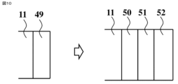
図10は、屈折率nfhで膜厚dfhがλ0/(4nfh)である単層被覆膜49を、それぞれ、屈折率n1で膜厚d1、屈折率n2で膜厚d2及び屈折率n3で膜厚d3である3層被覆膜で置換する場合の模式図である。図10に示すように、実効屈折率ncで波長λ0の光を出射する光半導体装置11の端面に形成された屈折率nfh(=1.977653)で膜厚dfh=λ0/(4nfh)の単層被覆膜49を、屈折率n1で膜厚d1である第1被覆膜50、屈折率n2で膜厚d2である第2被覆膜51、屈折率n3で膜厚d3である第3被覆膜52の3層被覆膜で置換する。単層被覆膜を3層被覆膜で置換する方法は、上述の低屈折率の場合と同様であり、以下の式(13)を解いて行う。

波長λ0=10μm、第1被覆膜50は屈折率がnflよりも低い屈折率n1=1.40であるYF3を、第2被覆膜51は屈折率がnflよりも高い屈折率n2=2.20であるZnSを、第3被覆膜52は屈折率がnflよりも低いn3=1.45であるCeF3を一例として式(13)を解くと、それぞれ、d1=370.115nm、d2=607.246nm、d3=395.897nmとなる。この場合の反射率の波長依存性を図11の一点鎖線54に示す。反射率は波長10μmにおいて1.0%となるが、この値は極小値ではなく、3層被覆膜の反射率の極小値Rmin
0は0.94561%である。
単層被覆膜の極小反射率R0:1.0%に対して、3層被覆膜の反射率の極小値Rmin
0が0.94561%と、単層被覆膜の極小反射率R0よりも低くなる。そこで、実施の形態1と同様に、3層被覆膜の反射率の極小値Rminを所望の極小反射率R0にすべく、設定反射率R1を1.057485%と高く設定する。設定反射率R1=1.057485%を実現するための単層被覆膜の屈折率nfh
1は、式(8)よりnfh
1=1.9833241と算出される。以下の式(14)を解いて各被覆膜の膜厚を計算すると、各膜厚は、d1=364.825nm、d2=614.601nm、d3=390.009nmと、それぞれ算出される。

この場合の反射率の波長依存性を、図11の二点鎖線55に示す。3層被覆膜の反射率の極小値Rminは、波長λmin=10.243μmにおいて1.0%と、所望の極小反射率である1.0%を得ることができる。
次に、極小反射率となる波長λminを、所望の波長λ0にする。各被覆膜の膜厚をλ0/λmin倍すると、d1=356.170nm、d2=600.021nm、d3=380.757nmと、それぞれ算出される。この場合の反射率の波長依存性を、図11の実線56に示す。波長λ0において極小反射率である1.0%となることが分かる。
なお、図11の破線53は、屈折率nfhで膜厚がλ0/(4nfh)である単層被覆膜に関する、反射率の波長依存性である。図11の実線56及び破線53は、完全には一致しないが、ほぼ同一の反射率の波長依存性を示すとともに、極小反射率及び極小反射率となる際の波長は完全に一致する。
極小反射率R0=1.0%及び波長λ0=10μmは例示であり、これらに限るものではなく、所望の数値に設定することができる。また。第1被覆膜50にYF3を、第2被覆膜51にZnSを、第3被覆膜52にCeF3を用いたが、これらに限るものではなく、屈折率がnfh及びnfh
1よりも高い材料が1つ以上、及び屈折率がnfh及びnfh
1よりも低い材料が1つ以上あれば良く、各材料の順序も任意に選ぶことができる。
以上より、所望の波長において所望の極小反射率を、屈折率が既知の材料を用いて実現できることが分かる。
以上より、所望の波長において所望の極小反射率を、屈折率が既知の材料を用いて実現できることが分かる。
<実施の形態2の効果>
以上、実施の形態2に係る光半導体装置の製造方法及び低反射率膜の設計方法によると、単層被覆膜を、特性行列を利用して3層の多層被覆膜によって置換することにより、所望の波長において所望の極小反射率に制御された低反射率膜を有する光半導体装置を製造することが可能となり、また、低反射率膜の設計方法を得ることが可能となる。
以上、実施の形態2に係る光半導体装置の製造方法及び低反射率膜の設計方法によると、単層被覆膜を、特性行列を利用して3層の多層被覆膜によって置換することにより、所望の波長において所望の極小反射率に制御された低反射率膜を有する光半導体装置を製造することが可能となり、また、低反射率膜の設計方法を得ることが可能となる。
なお、上述の光半導体装置の製造方法は、上記低反射率膜の設計方法の思想を利用するものであって、製造の上で多層被覆膜の各被覆膜が厳密に一致しなくても構わない。つまり、実施の形態2の設計方法によって設計し、光半導体装置に設けた低反射率膜の製造方法は本開示に含まれる。
実施の形態3.
実施の形態3では、屈折率の異なる4つ以上の材料を用い、所望の極小反射率を所望の波長で実現する方法について説明する。4つ以上の材料からなる多層被覆膜の一例として、5層被覆膜について説明する。
実施の形態3では、屈折率の異なる4つ以上の材料を用い、所望の極小反射率を所望の波長で実現する方法について説明する。4つ以上の材料からなる多層被覆膜の一例として、5層被覆膜について説明する。
実施の形態3では、極小反射率R0=0.01(1%)を一例として説明する。光半導体装置の実効屈折率ncが3.2とすると、式(2)より、屈折率nfl及び屈折率nfhは、それぞれ、1.618080及び1.977653と算出される。
先ず、屈折率nfl=1.618080の場合について説明する。単層被覆膜を、少なくとも1つは屈折率nflよりも屈折率が低い材料とし、少なくとも1つは屈折率nflよりも屈折率が高い材料となる5つの材料による5層被覆膜による置換を考える。
図12は、屈折率nflで膜厚dflがλ0/(4nfl)である単層被覆膜41を、屈折率n1で膜厚d1、屈折率n2で膜厚d2、屈折率n3で膜厚d3、屈折率n4で膜厚d4及び屈折率n5で膜厚d5である5層被覆膜で置換する場合の模式図である。図12に示すように、実効屈折率ncで波長λ0の光を出射する光半導体装置11の端面に形成された屈折率nflで膜厚dflがλ0/(4nfl)である単層被覆膜41を、屈折率n1で膜厚d1である第1被覆膜61、屈折率n2で膜厚d2である第2被覆膜62、屈折率n3で膜厚d3である第3被覆膜63、屈折率n4で膜厚d4である第4被覆膜64、屈折率n5で膜厚d5である第5被覆膜65の5層被覆膜で置換する。単層被覆膜を5層被覆膜で置換できるとすると、以下の式(15)で表されるように、両者の特性行列は等しくなる。


ただし、式(15)から算出される未知数は3つまでなので、5つの材料のうちの2つの材料の膜厚は、予め設定された膜厚としておく。ここでは、一例として第1被覆膜61及び第2被覆膜62の膜厚d1及びd2を、予め設定された膜厚とする。
波長λ0=10μm、第1被覆膜61は屈折率がnflよりも高い屈折率n1=1.70で膜厚d1=200nmであるCeO2、第2被覆膜62は屈折率がnflよりも高い屈折率n2=2.20で膜厚d2=100nmであるZnS、第3被覆膜63は屈折率がnflよりも低いn3=1.40で膜厚d3であるYF3、第4被覆膜64は屈折率がnflよりも高い屈折率n4=2.41で膜厚d4であるZnSe、第5被覆膜65は屈折率がnflよりも低いn5=1.45で膜厚d5であるCeF3を一例として式(15)を解くと、各被覆膜の膜厚は、それぞれ、d3=738.670nm、d4=151.598nm、d5=333.010nmとなる。
この場合の反射率の波長依存性を、図13の一点鎖線67に示す。反射率は波長10μmにおいて1.0%となるが、この値は極小値ではなく、5層被覆膜の反射率の極小値Rmin
0は0.998474%である。
単層被覆膜の極小反射率R0:1.0%に対して、5層被覆膜の反射率の極小値Rmin
0が0.998474%と、単層被覆膜の極小反射率R0よりも低くなる。そこで、5層被覆膜の反射率の極小値Rminを所望の極小反射率R0にすべく、設定反射率R1を1.00153%と高く設定する。この場合、式(5)より、設定反射率R1=1.00153%を実現するための単層被覆膜の屈折率nfl
1は、1.617955と算出される。以下の式(17)を解いて各被覆膜の膜厚を計算すると、それぞれ、d3=738.955nm、d4=151.533nm、d5=332.847nmと算出される。

この場合の反射率の波長依存性を、図13の二点鎖線68に示す。5層被覆膜の反射率の極小値Rminは、波長λmin=10.040μmにおいて1.0%と、所望の極小反射率である1.0%を得ることができる。
次に、極小反射率となる波長λminを、所望の波長λ0にする。各被覆膜の膜厚をそれぞれλ0/λmin倍すると、d1=199.203nm、d2=99.602nm.d3=736.011nm、d4=150.929nm、d5=331.521nmと、それぞれ算出される。なお、第1被覆膜61及び第2被覆膜62もλ0/λmin倍する。この場合の反射率の波長依存性を、図13の実線69に示す。波長λ0=10μmにおいて、極小反射率である1.0%となることが分かる。
なお、図13の破線66は、屈折率nflで膜厚がλ0/(4nfl)である単層被覆膜に関する、反射率の波長依存性である。図13の実線69及び破線66は、完全には一致しないが、ほぼ同一の反射率の波長依存性を示すと共に、極小反射率及び極小反射率となる際の波長は完全に一致する。
極小反射率R0=1.0%及び波長λ0=10μmは例示であり、これらに限るものではなく、所望の数値に設定することができる。また。上述の一例では、第1被覆膜61にCeO2を、第2被覆膜62にZnSを、第3被覆膜63にYF3を、第4被覆膜64にZnSeを、第5被覆膜65にCeF3を用いたが、これらに限るものではなく、屈折率がnfl及びnfl
1よりも高い材料が1つ以上及び屈折率がnfl及びnfl
1よりも低い材料が1つ以上あれば良く、各材料の順序も任意に選ぶことができる。
また、予め膜厚が設定された2つの被覆膜も、5層被覆膜の中で任意に選定することが可能である。実施の形態3では、4層以上の被覆膜の一例として5層被覆膜を例示したが、同様に行うことで、さらに多層被覆膜であっても、所望の波長において所望の極小反射率を実現できる。
同様に、屈折率nfh=1.977653の場合について説明する。単層被覆膜を、少なくとも1つは屈折率nfhよりも屈折率が低い材料とし、少なくとも1つは屈折率nfhよりも屈折率が高い材料とする5つの材料による5層被覆膜による置換を考える。
図14は、屈折率nfhで膜厚dfhがλ0/(4nfh)である単層被覆膜49を、屈折率n1で膜厚d1、屈折率n2で膜厚d2、屈折率n3で膜厚d3、屈折率n4で膜厚d4及び屈折率n5で膜厚d5である5層被覆膜で置換する場合の模式図である。図14に示すように、実効屈折率ncで波長λ0の光を出射する光半導体装置11の端面に形成された屈折率nfh(=1.977653)で膜厚dfh=λ0/(4nfh)である単層被覆膜49を、屈折率n1で膜厚d1である第1被覆膜71、屈折率n2で膜厚d2である第2被覆膜72、屈折率n3で膜厚d3である第3被覆膜73、屈折率n4で膜厚d4である第4被覆膜74、屈折率n5で膜厚d5である第5被覆膜75の5層被覆膜で置換する。単層被覆膜を5層被覆膜で置換する方法は、上述の低屈折率膜の場合と同様であり、以下の式(18)を解いて行う。

波長λ0=10μm、第1被覆膜71は屈折率がnfhよりも低い屈折率n1=1.70で膜厚d1=200nmであるCeO2、第2被覆膜72は屈折率がnfhよりも高い屈折率n2=2.20で膜厚d2=100nmであるZnS、第3被覆膜73は屈折率がnfhよりも低いn3=1.40で膜厚d3であるYF3、第4被覆膜74は屈折率がnfhよりも高い屈折率n4=2.41で膜厚d4であるZnSe、第5被覆膜75は屈折率がnfhよりも低いn5=1.45で膜厚d5であるCeF3を一例として式(18)を解くと、各被覆膜の膜厚は、それぞれ、d3=282.491nm、d4=387.869nm、d5=366.354nmとなる。
この場合の反射率の波長依存性を、図15の一点鎖線77に示す。反射率は波長10μmにおいて1.0%となるが、この値は極小値ではなく、5層被覆膜の反射率の極小値Rmin
0は0.975517%である。
単層被覆膜の極小反射率R0:1.0%に対して、5層被覆膜の極小値Rmin
0が0.975517%と、単層被覆膜の極小反射率R0よりも低くなる。そこで、5層被覆膜の極小値Rminを所望の極小反射率R0にすべく、設定反射率R1を1.025357%と高く設定する。この場合、設定反射率R1=1.025357%を実現するための単層被覆膜の屈折率nfh
1は、式(8)よりnfh
1=1.9801717と算出される。以下の式(19)を解いて各被覆膜の膜厚を計算すると、d3=280.332nm、d4=389.708nm、d5=365.369nmと、それぞれ算出される。

この場合の反射率の波長依存性を、図15の二点鎖線78に示す。5層被覆膜の極小値Rminは、波長λmin=10.159μmにおいて1.0%と、所望の極小反射率である1.0%を得ることができる。
次に、極小反射率となる波長λminを、所望の波長λ0にする。各膜厚をλ0/λmin倍すると、各被覆膜の膜厚は、d1=196.870nm、d2=98.435nm.d3=275.944nm、d4=383.609nm、d5=359.651nmと、それぞれ算出される。なお、第1被覆膜71及び第2被覆膜72も、λ0/λmin倍する。この場合の反射率の波長依存性を、図15の実線79に示す。波長λ0=10μmにおいて極小反射率である1.0%となることが分かる。
なお、図15の破線76は、屈折率nfhで膜厚がλ0/(4nfh)である単層被覆膜49に関する、反射率の波長依存性である。図15の実線79及び破線76は、完全には一致しないが、ほぼ同一の反射率の波長依存性を示すとともに、極小反射率及び極小反射率となる際の波長は完全に一致する。
極小反射率R0=1.0%及び波長λ0=10μmは例示であり、これらに限るものではなく、所望の数値に設定することができる。また。第1被覆膜71にCeO2を、第2被覆膜72にZnSを、第3被覆膜73にYF3を、第4被覆膜74にZnSeを、第5被覆膜75にCeF3を用いたが、これらに限るものではなく、屈折率がnfh及びnfh
1よりも高い材料が1つ以上及び屈折率がnfh及びnfh
1よりも低い材料が1つ以上あれば良く、各材料の順序も任意に選ぶことができる。
また、予め膜厚が設定された2つの被覆膜も、5層被覆膜の中で任意に選定することが可能である。実施の形態3では、4層以上の被覆膜の一例として5層被覆膜を例示したが、同様に行うことで、さらに多層被覆膜であっても、所望の波長において所望の極小反射率を実現できる。
<実施の形態3の効果>
以上、実施の形態3に係る光半導体装置の製造方法及び低反射率膜の設計方法によると、単層被覆膜を、特性行列を利用して5層の多層被覆膜によって置換することにより、所望の波長において所望の極小反射率に制御された低反射率膜を有する光半導体装置を製造することが可能となり、また、低反射率膜の設計方法を得ることが可能となる。
以上、実施の形態3に係る光半導体装置の製造方法及び低反射率膜の設計方法によると、単層被覆膜を、特性行列を利用して5層の多層被覆膜によって置換することにより、所望の波長において所望の極小反射率に制御された低反射率膜を有する光半導体装置を製造することが可能となり、また、低反射率膜の設計方法を得ることが可能となる。
なお、上述の光半導体装置の製造方法は、上記低反射率膜の設計方法の思想を利用するものであって、製造の上で多層被覆膜の各被覆膜が厳密に一致しなくても構わない。つまり、以下の設計方法によって設計し光半導体装置に設けた低反射率膜の製造方法は本開示に含まれる。
被覆膜数が3を超える多層被覆膜の場合は、超えた被覆膜数の膜厚を予め設定する。その上で、所望の波長(λ0)で所望の極小反射率(R0)を得るのに、所望の極小反射率(R0)となる単層被覆膜を多層被覆膜で置換し、多層被覆膜の反射率の極小値(Rmin
0)及び極小反射率となる波長(λmin)を算出する。次に、多層被覆膜の反射率の極小値(Rmin)が所望の極小反射率(R0)と一致するように、単層被覆膜の極小反射率R1をR0+ΔR0と設定する。さらに、所望の波長(λ0)で所望の極小反射率(R0)となるように、多層被覆膜の各膜厚を算出する。
実施の形態4.
光半導体装置のミラー損失は、以下の式(20)で定義される。
光半導体装置のミラー損失は、以下の式(20)で定義される。

式(20)において、Rf、Rr及びLは、それぞれ、前端面反射率、後端面反射率及び共振器長である。ミラー損失の帯域が狭いことを必要とするような用途では、極小反射率の近傍の帯域を狭くする必要がある。
図16は、実施の形態2(図8)に示した極小反射率を一例として、極小反射率の近傍の帯域を狭くする方法を示す模式図である。図16に示すように、実施の形態4では、屈折率がnaで膜厚daがλ0/(2na)である被覆膜81が設けられている点に特徴がある。その他の各被覆膜は、実施の形態2の図8に示される各被覆膜と同一である。
実施の形態4の4層被覆膜の特性行列は、以下の式(21)で表される。
実施の形態4の4層被覆膜の特性行列は、以下の式(21)で表される。



挿入された被覆膜81の材料の一例として、屈折率naが1.70であるCeO2とする。被覆膜81の膜厚daは、仮に波長λ0=10μmにおいてda=λ0/(2na)となる2941.176nmとする。
実施の形態2において、設定反射率R1を1.0165%とし、式(12)を解いて各被覆膜の膜厚として算出した、d1=641.123nm、d2=205.474nm、d3=765.332nmからなる3層被覆膜の第2番目の被覆膜と第3番目の被覆膜との間に上述の被覆膜81を挿入した場合の反射率の波長依存性を、図17の一点鎖線82に示す。4層被覆膜の反射率の極小値Rmin
0は、0.9609%となる。
そこで、λminにおいて極小反射率R0を1.0%にすべく、設定反射率R1を1.05761%として式(12)を解くと、各被覆膜の膜厚は、d1=642.718nm、d2=201.981nm、d3=769.510nmとそれぞれ算出され、波長λmin=9.908μmにおいて4層被覆膜の反射率の極小値Rmin=1.0%となる(図17の二点鎖線83)。なお、このとき、第2被覆膜43と第3被覆膜44の間に挿入した被覆膜81の屈折率naは1.70であり、膜厚daは2941.176nmである。
次に、各被覆膜の膜厚をλ0/λmin倍すると、各被覆膜の膜厚は、それぞれ、d1=648.686nm、d2=203.856nm、da=2968.486nm、d3=776.655nmと算出される。この場合の反射率の波長依存性を、図17の実線84に示す。波長λ0=10μmにおいて極小反射率である1.0%となることが分かる。
比較のため、実施の形態2の3層被覆膜の反射率の波長依存性を、図17の破線48に示す。所望の波長λ0の近傍において、反射率帯域が狭くなっていることが分かる。
同様に、実施の形態2(図10)に示した極小反射率を一例として、屈折率が高い場合(nfh)について、極小反射率の近傍の帯域を狭くする方法を、以下に説明する。
図18は被覆膜の構成を示す模式図である。図18において、被覆膜81は、屈折率がnaで膜厚daがλ0/(2na)である。その他の各被覆膜は、実施の形態2の図10と同一である。
実施の形態2において、設定反射率R1を1.057485%とし、式(14)を解いて各被覆膜の膜厚として算出した、それぞれd1=364.825nm、d2=614.601nm、d3=390.009nmからなる3層被覆膜の第2被覆膜51と第3被覆膜52との間に、上述の被覆膜81を挿入した場合の反射率の波長依存性を、図19の一点鎖線85に示す。4層被覆膜の反射率の極小値Rmin
0は、0.9950%となる。
そこで、波長λminにおいて極小反射率を1.0%にすべく、設定反射率R1を1.0627%として式(14)を解くと、各被覆膜の膜厚は、それぞれd1=364.348nm、d2=615.265nm、d3=389.478nmと算出され、波長λmin=10.110μmにおいて4層被覆膜の反射率の極小値Rmin=1.0%となる(図19の二点鎖線86)。なお、このとき、第2被覆膜51と第3被覆膜52の間に挿入した被覆膜81の屈折率naは1.70であり、膜厚daは2941.176nmである。
次に、各被覆膜の膜厚をλ0/λmin倍とすると、d1=360.384nm、d2=608.571nm、da=2909.175nm、d3=385.240nmと算出される。この場合の反射率の波長依存性を、図19の実線87に示す。波長λ0=10μmにおいて、極小反射率である1.0%となることが分かる。
比較のため、実施の形態2の3層膜の反射率の波長依存性を、図19の破線56に示す。所望の波長λ0の近傍において、反射率帯域が狭くなっていることが分かる。
実施の形態4では、所望の屈折率naで膜厚daがλ0/(2na)である被覆膜81を挿入したが、被覆膜81の膜厚はλ0/(4na)よりも厚く、3λ0/(4na)よりも薄いものであれば、反射率帯域を狭くすることが可能である。
また、実施の形態4では、3層被覆膜の特性行列を解いて各被覆膜の膜厚を導出した後に、被覆膜を挿入して反射率の波長依存性を算出し、4層被覆膜の反射率の極小値Rmin
0を所望の極小反射率R0に合わせ、その後、所望の波長λ0において所望の極小反射率R0となるようにした。しかしながら、実施の形態3において示したように、予め4層被覆膜と想定し、挿入した被覆膜の膜厚をda=λ0/(2na)又はda=λmin/(2na)と設定しておいて、3層被覆膜の各膜厚を決定しても良い。
さらに、実施の形態4では、第2被覆膜と第3被覆膜の間に、da=λ0/(2na)である被覆膜を挿入したが、他の界面、例えば光半導体装置と第1被覆膜、第1被覆膜と第2被覆膜、第3被覆膜と空気(自由空間)の間であっても良いし、光半導体装置と第1被覆膜の間及び第2被覆膜と第3被覆膜の間等の複数の界面に挿入しても良い。
<実施の形態4の効果>
以上、実施の形態4に係る光半導体装置の製造方法及び低反射率膜の設計方法によると、単層被覆膜を、特性行列を利用して4層の多層被覆膜によって置換することにより、所望の波長において所望の極小反射率に制御された低反射率膜を有する光半導体装置を製造することが可能となり、また、低反射率膜の設計方法を得ることが可能となる。
以上、実施の形態4に係る光半導体装置の製造方法及び低反射率膜の設計方法によると、単層被覆膜を、特性行列を利用して4層の多層被覆膜によって置換することにより、所望の波長において所望の極小反射率に制御された低反射率膜を有する光半導体装置を製造することが可能となり、また、低反射率膜の設計方法を得ることが可能となる。
なお、上述の光半導体装置の製造方法は、上記低反射率膜の設計方法の思想を利用するものであって、製造の上で多層被覆膜の各被覆膜が厳密に一致しなくても構わない。つまり、以下の設計方法によって設計し光半導体装置に設けた低反射率膜の製造方法は本開示に含まれる。
所望の波長がλ0で挿入する被覆膜の屈折率がnaの場合、挿入する被覆膜の膜厚をλ0/(4na)よりも厚く、3λ0/(4na)よりも薄い範囲で予め設定する。その上で、所望の波長(λ0)で所望の極小反射率(R0)を得るのに、所望の極小反射率(R0)となる単層被覆膜を多層被覆膜で置換し、多層被覆膜の反射率の極小値(Rmin
0)及び極小反射率となる波長(λmin)を算出する。次に、多層被覆膜の反射率の極小値(Rmin)が所望の極小反射率(R0)と一致するように単層被覆膜の極小反射率R1をR0+ΔR0と設定する。さらに、所望の波長(λ0)で所望の極小反射率(R0)となるように多層被覆膜の各膜厚を算出する。
実施の形態1から4において、所望の極小反射率R0である0.5%、1.0%の数値、及び所望の波長λ0である10μmは一例であって、これらに限るものではなく、他の所望の極小反射率及び所望の波長において同様に設計することができる。
実施の形態1から4において、多層被覆膜で置換した場合の多層被覆膜の反射率の極小値Rmin
0は、単層被覆膜の極小反射率R0よりも低いが、仮に高い場合であっても同様にして、所望の波長で所望の極小反射率を実現することができる。
本開示は、様々な例示的な実施の形態及び実施例が記載されているが、1つ、または複数の実施の形態に記載された様々な特徴、態様、及び機能は特定の実施の形態の適用に限られるのではなく、単独で、または様々な組み合わせで実施の形態に適用可能である。
従って、例示されていない無数の変形例が、本開示における技術の範囲内において想定される。例えば、少なくとも1つの構成要素を変形する場合、追加する場合または省略する場合、さらには、少なくとも1つの構成要素を抽出し、他の実施の形態の構成要素と組み合わせる場合が含まれるものとする。
1 n型第1電極、2 n型InP基板、3 n型InPバッファ層、4 n型GaInAs第1光閉じ込め層、5 コア領域、6 n型GaInAs第2光閉じ込め層、7 n型InPクラッド層、8 n型GaInAsコンタクト層、9 n型第2電極、10 低反射率膜、11 光半導体装置、12、31、41、49 単層被覆膜、13、32、42、50、61、71 第1被覆膜、14、33、43、51、62、72 第2被覆膜、15、34、44、52、63、73 第3被覆膜、21、21a、21b、35、45、48、53、56、66、76 破線、21a 点線、22、22a、36、46、54、67、77、82、85 一点鎖線、23、23a、37、47、55、68、78、83、86 二点鎖線、24、24a、38、48、56、69、79、84、87 実線、64、74 第4被覆膜、65、75 第5被覆膜、81 被覆膜、100 量子カスケードレーザ装置
Claims (18)
- 実効屈折率がncであり、所望の波長λ0において所望の極小反射率である極小反射率R0となる低反射率膜が形成された光半導体装置の製造方法であって、
屈折率nflが以下の式で表され、

予め設定された設定反射率R1を実現する単層からなる被覆膜の屈折率nfl 1が、以下の式で表され、
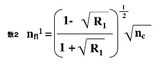
前記波長λminにおける前記極小値Rminを前記波長λ0における前記極小反射率R0と一致させることによって得られる前記3層以上の被覆膜の各膜厚に基づき多層被覆膜を端面に形成することを特徴とする光半導体装置の製造方法。 - 実効屈折率がncであり、所望の波長λ0において所望の極小反射率である極小反射率R0となる低反射率膜が形成された光半導体装置の製造方法であって、
屈折率nfhが以下の式で表され、
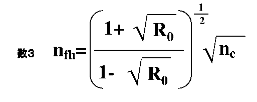
予め設定された設定反射率R1を実現する単層からなる被覆膜の屈折率nfh 1が、以下の式で表され、

前記波長λminにおける前記極小値Rminを前記波長λ0における前記極小反射率R0と一致させることによって得られる前記3層以上の被覆膜の各膜厚に基づき多層被覆膜を端面に形成することを特徴とする光半導体装置の製造方法。 - 屈折率がnfl及びnfl 1よりも低い少なくとも1つの材料からなる被覆膜と、屈折率がnfl及びnfl 1よりも高い他の少なくとも1つの材料からなる被覆膜を含む3層の被覆膜を端面に形成することを特徴とする請求項1に記載の光半導体装置の製造方法。
- 屈折率がnfh及びnfh 1よりも低い少なくとも1つの材料からなる被覆膜と、屈折率がnfh及びnfh 1よりも高い他の少なくとも1つの材料からなる被覆膜を含む3層の被覆膜を端面に形成することを特徴とする請求項2に記載の光半導体装置の製造方法。
- 屈折率がnfl及びnfl 1よりも低い少なくとも1つの材料からなる被覆膜と、屈折率がnfl及びnfl 1よりも高い他の少なくとも1つの材料からなる被覆膜とを含む3種類の材料から成る3層の被覆膜を端面に形成することを特徴とする請求項1に記載の光半導体装置の製造方法。
- 屈折率がnfh及びnfh 1よりも低い少なくとも1つの材料からなる被覆膜と、屈折率がnfh及びnfh 1よりも高い他の少なくとも1つの材料からなる被覆膜とを含む3種類の材料から成る3層の被覆膜を端面に形成することを特徴とする請求項2に記載の光半導体装置の製造方法。
- 屈折率がnfl及びnfl 1よりも低い少なくとも1つの材料と、屈折率がnfl及びnfl 1よりも高い他の少なくとも1つの材料とを含む4種類以上の材料からなり、前記4種類以上の材料のうち3種類の材料でそれぞれ構成された3層の被覆膜、及び3種類以外の材料からなり予め設定された膜厚を有する被覆膜を含む多層被覆膜を端面に形成することを特徴とする請求項1に記載の光半導体装置の製造方法。
- 屈折率がnfh及びnfh 1よりも低い少なくとも1つの材料と、屈折率がnfh及びnfh 1よりも高い他の少なくとも1つの材料とを含む4種類以上の材料からなり、前記4種類以上の材料のうち3種類の材料でそれぞれ構成された3層の被覆膜、及び3種類以外の材料からなり予め設定された膜厚を有する被覆膜を含む多層被覆膜を端面に形成することを特徴とする請求項2に記載の光半導体装置の製造方法。
- 屈折率がnaであり、膜厚がλ0/(4na)よりも厚く3λ0/(4na)よりも薄い被覆膜を、前記多層被覆膜と端面の間、前記多層被覆膜の各被覆膜の間、または、前記多層被覆膜の最表面に設けることを特徴とする請求項3から8のいずれか1項に記載の光半導体装置の製造方法。
- 実効屈折率がncである光半導体装置の端面に、ゼロを除く所望の極小反射率である極小反射率R0を有する低反射率膜の設計方法であって、
屈折率nflが以下の式により、屈折率nflを算出するステップと、

予め設定された設定反射率R1を実現する単層からなる被覆膜の屈折率nfl 1を、以下の式を用いて算出するステップと、
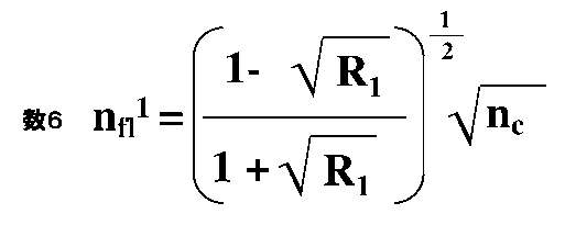
前記波長λminにおける前記極小値Rminを波長λ0における前記極小反射率R0と一致させることによって得られる前記3層以上の被覆膜の各膜厚に基づき多層被覆膜の各膜厚を決定するステップと、
を備える低反射率膜の設計方法。 - 実効屈折率がncである光半導体装置の端面に、ゼロを除く所望の極小反射率である極小反射率R0を有する低反射率膜の設計方法であって、
屈折率nfhが以下の式により、屈折率nfhを算出するステップと、
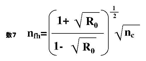
予め設定された設定反射率R1を実現する単層からなる被覆膜の屈折率nfh 1を、以下の式を用いて算出するステップと、

前記波長λminにおける前記極小値Rminを前記波長λ0における前記極小反射率R0と一致させることによって得られる前記3層以上の被覆膜の各膜厚に基づき多層被覆膜の各膜厚を決定するステップと、
を備える低反射率膜の設計方法。 - 屈折率がnfl及びnfl 1よりも低い少なくとも1つの材料からなる被覆膜と、屈折率がnfl及びnfl 1よりも高い他の少なくとも1つの材料からなる被覆膜を含む3層の被覆膜を端面に形成することを特徴とする請求項10に記載の低反射率膜の設計方法。
- 屈折率がnfh及びnfh 1よりも低い少なくとも1つの材料からなる被覆膜と、屈折率がnfh及びnfh 1よりも高い他の少なくとも1つの材料からなる被覆膜を含む3層の被覆膜を端面に形成することを特徴とする請求項11に記載の低反射率膜の設計方法。
- 屈折率がnfl及びnfl 1よりも低い少なくとも1つの材料からなる被覆膜と、屈折率がnfl及びnfl 1よりも高い他の少なくとも1つの材料からなる被覆膜とを含む3種類の材料から成る3層の被覆膜を端面に形成することを特徴とする請求項10に記載の低反射率膜の設計方法。
- 屈折率がnfh及びnfh 1よりも低い少なくとも1つの材料からなる被覆膜と、屈折率がnfh及びnfh 1よりも高い他の少なくとも1つの材料からなる被覆膜とを含む3種類の材料から成る3層の被覆膜を端面に形成することを特徴とする請求項11に記載の低反射率膜の設計方法。
- 屈折率がnfl及びnfl 1よりも低い少なくとも1つの材料と、屈折率がnfl及びnfl 1よりも高い他の少なくとも1つの材料とを含む4種類以上の材料からなり、前記4種類以上の材料のうち3種類の材料でそれぞれ構成された3層の被覆膜、及び3種類以外の材料からなり予め設定された膜厚を有する被覆膜を含む多層被覆膜を端面に形成することを特徴とする請求項10に記載の低反射率膜の設計方法。
- 屈折率がnfh及びnfh 1よりも低い少なくとも1つの材料と、屈折率がnfh及びnfh 1よりも高い他の少なくとも1つの材料とを含む4種類以上の材料からなり、前記4種類以上の材料のうち3種類の材料でそれぞれ構成された3層の被覆膜、及び3種類以外の材料からなり予め設定された膜厚を有する被覆膜を含む多層被覆膜を端面に形成することを特徴とする請求項11に記載の低反射率膜の設計方法。
- 屈折率がnaであり、膜厚がλ0/(4na)よりも厚く3λ0/(4na)よりも薄い被覆膜を、前記多層被覆膜と端面の間、前記多層被覆膜の各被覆膜の間、または、前記多層被覆膜の最表面に設けることを特徴とする請求項12から17のいずれか1項に記載の低反射率膜の設計方法。
Priority Applications (3)
| Application Number | Priority Date | Filing Date | Title |
|---|---|---|---|
| CN202380098884.6A CN121488371A (zh) | 2023-07-12 | 2023-07-12 | 光半导体装置的制造方法以及低反射率膜的设计方法 |
| PCT/JP2023/025764 WO2025013255A1 (ja) | 2023-07-12 | 2023-07-12 | 光半導体装置の製造方法及び低反射率膜の設計方法 |
| JP2023554334A JP7378692B1 (ja) | 2023-07-12 | 2023-07-12 | 光半導体装置の製造方法及び低反射率膜の設計方法 |
Applications Claiming Priority (1)
| Application Number | Priority Date | Filing Date | Title |
|---|---|---|---|
| PCT/JP2023/025764 WO2025013255A1 (ja) | 2023-07-12 | 2023-07-12 | 光半導体装置の製造方法及び低反射率膜の設計方法 |
Publications (1)
| Publication Number | Publication Date |
|---|---|
| WO2025013255A1 true WO2025013255A1 (ja) | 2025-01-16 |
Family
ID=88729162
Family Applications (1)
| Application Number | Title | Priority Date | Filing Date |
|---|---|---|---|
| PCT/JP2023/025764 Pending WO2025013255A1 (ja) | 2023-07-12 | 2023-07-12 | 光半導体装置の製造方法及び低反射率膜の設計方法 |
Country Status (3)
| Country | Link |
|---|---|
| JP (1) | JP7378692B1 (ja) |
| CN (1) | CN121488371A (ja) |
| WO (1) | WO2025013255A1 (ja) |
Families Citing this family (2)
| Publication number | Priority date | Publication date | Assignee | Title |
|---|---|---|---|---|
| WO2025224910A1 (ja) * | 2024-04-25 | 2025-10-30 | 三菱電機株式会社 | 光半導体装置及び光半導体装置の製造方法 |
| JP7742959B1 (ja) | 2024-04-25 | 2025-09-22 | 三菱電機株式会社 | 光半導体装置及び光半導体装置の製造方法 |
Citations (5)
| Publication number | Priority date | Publication date | Assignee | Title |
|---|---|---|---|---|
| JPH05243689A (ja) * | 1992-02-27 | 1993-09-21 | Mitsubishi Electric Corp | 半導体光素子 |
| JP2006156729A (ja) * | 2004-11-30 | 2006-06-15 | Mitsubishi Electric Corp | コーティング膜の膜厚設計方法及び半導体光装置 |
| JP2010123995A (ja) * | 2002-09-27 | 2010-06-03 | Mitsubishi Electric Corp | 半導体光素子 |
| JP2011176380A (ja) * | 2002-03-08 | 2011-09-08 | Mitsubishi Electric Corp | 光半導体素子のコーティング膜の設計方法 |
| JP7183484B1 (ja) * | 2022-04-14 | 2022-12-05 | 三菱電機株式会社 | 光半導体装置の製造方法及び光半導体装置用反射防止膜の設計方法 |
-
2023
- 2023-07-12 WO PCT/JP2023/025764 patent/WO2025013255A1/ja active Pending
- 2023-07-12 CN CN202380098884.6A patent/CN121488371A/zh active Pending
- 2023-07-12 JP JP2023554334A patent/JP7378692B1/ja active Active
Patent Citations (5)
| Publication number | Priority date | Publication date | Assignee | Title |
|---|---|---|---|---|
| JPH05243689A (ja) * | 1992-02-27 | 1993-09-21 | Mitsubishi Electric Corp | 半導体光素子 |
| JP2011176380A (ja) * | 2002-03-08 | 2011-09-08 | Mitsubishi Electric Corp | 光半導体素子のコーティング膜の設計方法 |
| JP2010123995A (ja) * | 2002-09-27 | 2010-06-03 | Mitsubishi Electric Corp | 半導体光素子 |
| JP2006156729A (ja) * | 2004-11-30 | 2006-06-15 | Mitsubishi Electric Corp | コーティング膜の膜厚設計方法及び半導体光装置 |
| JP7183484B1 (ja) * | 2022-04-14 | 2022-12-05 | 三菱電機株式会社 | 光半導体装置の製造方法及び光半導体装置用反射防止膜の設計方法 |
Also Published As
| Publication number | Publication date |
|---|---|
| CN121488371A (zh) | 2026-02-06 |
| JPWO2025013255A1 (ja) | 2025-01-16 |
| JP7378692B1 (ja) | 2023-11-13 |
Similar Documents
| Publication | Publication Date | Title |
|---|---|---|
| KR100668096B1 (ko) | 반도체 레이저장치 | |
| WO2025013255A1 (ja) | 光半導体装置の製造方法及び低反射率膜の設計方法 | |
| JP3637081B2 (ja) | 同調可能な外部空洞型レーザの出力特性を最適化するための方法と装置 | |
| JP2004140240A (ja) | 半導体レーザ | |
| KR101098724B1 (ko) | 다파장 반도체 레이저 및 그 제조 방법 | |
| US6487227B1 (en) | Semiconductor laser | |
| CN104201566B (zh) | 一种具有高单纵模成品率的脊波导分布反馈半导体激光器 | |
| JP7183484B1 (ja) | 光半導体装置の製造方法及び光半導体装置用反射防止膜の設計方法 | |
| JP2001196685A (ja) | 半導体光素子装置 | |
| JP2009176812A (ja) | 半導体レーザ | |
| JP2000277851A (ja) | 分布帰還型半導体レーザ | |
| WO2025013254A1 (ja) | 量子カスケードレーザ装置及び量子カスケードレーザ装置の製造方法 | |
| KR100550924B1 (ko) | 다파장 레이저 다이오드 | |
| KR100528857B1 (ko) | 반도체 광소자장치 및 그것을 사용한 반도체 레이저 모듈 | |
| JP7742959B1 (ja) | 光半導体装置及び光半導体装置の製造方法 | |
| JP2006128475A (ja) | 半導体レーザ | |
| WO2025224910A1 (ja) | 光半導体装置及び光半導体装置の製造方法 | |
| CN222072442U (zh) | 一种半导体激光器 | |
| EP4492592B1 (en) | Semiconductor light-emitting element and external resonator type laser module | |
| US20240146035A1 (en) | Semiconductor laser device | |
| CN101257187B (zh) | 半导体激光装置 | |
| JP4595711B2 (ja) | 半導体レーザ | |
| CN120341688A (zh) | 一种半导体激光器 | |
| CN117199992A (zh) | 一种利用窄带宽反射器制造单模激光二极管的方法 | |
| JP5377432B2 (ja) | 半導体光素子装置 |
Legal Events
| Date | Code | Title | Description |
|---|---|---|---|
| WWE | Wipo information: entry into national phase |
Ref document number: 2023554334 Country of ref document: JP |
|
| 121 | Ep: the epo has been informed by wipo that ep was designated in this application |
Ref document number: 23945129 Country of ref document: EP Kind code of ref document: A1 |
|
| NENP | Non-entry into the national phase |
Ref country code: DE |