WO2025009271A1 - 発光装置およびその製造方法 - Google Patents
発光装置およびその製造方法 Download PDFInfo
- Publication number
- WO2025009271A1 WO2025009271A1 PCT/JP2024/017972 JP2024017972W WO2025009271A1 WO 2025009271 A1 WO2025009271 A1 WO 2025009271A1 JP 2024017972 W JP2024017972 W JP 2024017972W WO 2025009271 A1 WO2025009271 A1 WO 2025009271A1
- Authority
- WO
- WIPO (PCT)
- Prior art keywords
- nitride semiconductor
- layer
- substrate
- emitting device
- light emitting
- Prior art date
- Legal status (The legal status is an assumption and is not a legal conclusion. Google has not performed a legal analysis and makes no representation as to the accuracy of the status listed.)
- Ceased
Links
Images


Classifications
-
- H—ELECTRICITY
- H10—SEMICONDUCTOR DEVICES; ELECTRIC SOLID-STATE DEVICES NOT OTHERWISE PROVIDED FOR
- H10H—INORGANIC LIGHT-EMITTING SEMICONDUCTOR DEVICES HAVING POTENTIAL BARRIERS
- H10H20/00—Individual inorganic light-emitting semiconductor devices having potential barriers, e.g. light-emitting diodes [LED]
- H10H20/80—Constructional details
- H10H20/81—Bodies
- H10H20/819—Bodies characterised by their shape, e.g. curved or truncated substrates
- H10H20/82—Roughened surfaces, e.g. at the interface between epitaxial layers
-
- H—ELECTRICITY
- H10—SEMICONDUCTOR DEVICES; ELECTRIC SOLID-STATE DEVICES NOT OTHERWISE PROVIDED FOR
- H10H—INORGANIC LIGHT-EMITTING SEMICONDUCTOR DEVICES HAVING POTENTIAL BARRIERS
- H10H20/00—Individual inorganic light-emitting semiconductor devices having potential barriers, e.g. light-emitting diodes [LED]
- H10H20/01—Manufacture or treatment
- H10H20/011—Manufacture or treatment of bodies, e.g. forming semiconductor layers
- H10H20/013—Manufacture or treatment of bodies, e.g. forming semiconductor layers having light-emitting regions comprising only Group III-V materials
- H10H20/0133—Manufacture or treatment of bodies, e.g. forming semiconductor layers having light-emitting regions comprising only Group III-V materials with a substrate not being Group III-V materials
- H10H20/01335—Manufacture or treatment of bodies, e.g. forming semiconductor layers having light-emitting regions comprising only Group III-V materials with a substrate not being Group III-V materials the light-emitting regions comprising nitride materials
-
- H—ELECTRICITY
- H10—SEMICONDUCTOR DEVICES; ELECTRIC SOLID-STATE DEVICES NOT OTHERWISE PROVIDED FOR
- H10H—INORGANIC LIGHT-EMITTING SEMICONDUCTOR DEVICES HAVING POTENTIAL BARRIERS
- H10H20/00—Individual inorganic light-emitting semiconductor devices having potential barriers, e.g. light-emitting diodes [LED]
- H10H20/01—Manufacture or treatment
- H10H20/036—Manufacture or treatment of packages
- H10H20/0363—Manufacture or treatment of packages of optical field-shaping means
-
- H—ELECTRICITY
- H10—SEMICONDUCTOR DEVICES; ELECTRIC SOLID-STATE DEVICES NOT OTHERWISE PROVIDED FOR
- H10H—INORGANIC LIGHT-EMITTING SEMICONDUCTOR DEVICES HAVING POTENTIAL BARRIERS
- H10H20/00—Individual inorganic light-emitting semiconductor devices having potential barriers, e.g. light-emitting diodes [LED]
- H10H20/80—Constructional details
- H10H20/81—Bodies
- H10H20/811—Bodies having quantum effect structures or superlattices, e.g. tunnel junctions
- H10H20/812—Bodies having quantum effect structures or superlattices, e.g. tunnel junctions within the light-emitting regions, e.g. having quantum confinement structures
-
- H—ELECTRICITY
- H10—SEMICONDUCTOR DEVICES; ELECTRIC SOLID-STATE DEVICES NOT OTHERWISE PROVIDED FOR
- H10H—INORGANIC LIGHT-EMITTING SEMICONDUCTOR DEVICES HAVING POTENTIAL BARRIERS
- H10H20/00—Individual inorganic light-emitting semiconductor devices having potential barriers, e.g. light-emitting diodes [LED]
- H10H20/80—Constructional details
- H10H20/81—Bodies
- H10H20/822—Materials of the light-emitting regions
- H10H20/824—Materials of the light-emitting regions comprising only Group III-V materials, e.g. GaP
- H10H20/825—Materials of the light-emitting regions comprising only Group III-V materials, e.g. GaP containing nitrogen, e.g. GaN
-
- H—ELECTRICITY
- H10—SEMICONDUCTOR DEVICES; ELECTRIC SOLID-STATE DEVICES NOT OTHERWISE PROVIDED FOR
- H10H—INORGANIC LIGHT-EMITTING SEMICONDUCTOR DEVICES HAVING POTENTIAL BARRIERS
- H10H20/00—Individual inorganic light-emitting semiconductor devices having potential barriers, e.g. light-emitting diodes [LED]
- H10H20/80—Constructional details
- H10H20/85—Packages
- H10H20/855—Optical field-shaping means, e.g. lenses
-
- H—ELECTRICITY
- H10—SEMICONDUCTOR DEVICES; ELECTRIC SOLID-STATE DEVICES NOT OTHERWISE PROVIDED FOR
- H10H—INORGANIC LIGHT-EMITTING SEMICONDUCTOR DEVICES HAVING POTENTIAL BARRIERS
- H10H20/00—Individual inorganic light-emitting semiconductor devices having potential barriers, e.g. light-emitting diodes [LED]
- H10H20/01—Manufacture or treatment
- H10H20/011—Manufacture or treatment of bodies, e.g. forming semiconductor layers
- H10H20/019—Removal of at least a part of a substrate on which semiconductor layers have been formed
Definitions
- One embodiment of the present invention relates to a light-emitting device that uses a nitride semiconductor. Also, one embodiment of the present invention relates to a method for manufacturing a light-emitting device that uses a nitride semiconductor.
- Nitride semiconductors such as GaN and InGaN are widely used as light-emitting layers with a multiple quantum well (MQW) structure in blue or green light-emitting diodes.
- MQW multiple quantum well
- the In ratio in the nitride semiconductor must be high.
- MOCVD metalorganic chemical vapor deposition
- increasing the In ratio in the nitride semiconductor causes phase separation and reduces the light-emitting efficiency.
- MOCVD metalorganic chemical vapor deposition
- the In ratio in the MQW structure becomes high, polarization occurs between the well layer and the barrier layer due to lattice distortion. As a result, current dependency occurs due to the quantum confined Stark effect, and the emission wavelength shifts to shorter wavelengths.
- a light emitting device includes a ScAlMgO4 substrate including a first surface and a second surface opposite to the first surface, an undoped nitride semiconductor layer on the second surface of the ScAlMgO4 substrate, and a light emitting layer on the undoped nitride semiconductor layer, the light emitting layer having an MQW structure in which well layers including InxGa (1-x) N (0.30 ⁇ x ⁇ 0.50) and barrier layers including InyGa (1-y) N (0 ⁇ y ⁇ x) are alternately stacked, and a concave-convex pattern is provided on the first surface side.
- a method for manufacturing a light emitting device includes forming an anti-degassing layer on a first surface of a ScAlMgO4 support substrate, forming an undoped nitride semiconductor layer on a second surface of the ScAlMgO4 support substrate opposite to the first surface, and alternately depositing well layers containing InxGa (1-x) N (0.30 ⁇ x ⁇ 0.50) and barrier layers containing InyGa (1-y) N (0 ⁇ y ⁇ x) by sputtering on the undoped nitride semiconductor layer to form a light emitting layer having an MQW structure.
- 1 is a schematic cross-sectional view showing a configuration of a light-emitting device according to one embodiment of the present invention.
- 1 is a schematic cross-sectional view showing a configuration of a light-emitting layer of a light-emitting device according to one embodiment of the present invention.
- 4 is a flowchart illustrating a method for manufacturing a light emitting device according to an embodiment of the present invention.
- 5A to 5C are schematic cross-sectional views illustrating a method for manufacturing a light emitting device according to one embodiment of the present invention.
- 5A to 5C are schematic cross-sectional views illustrating a method for manufacturing a light emitting device according to one embodiment of the present invention.
- 5A to 5C are schematic cross-sectional views illustrating a method for manufacturing a light emitting device according to one embodiment of the present invention.
- 5A to 5C are schematic cross-sectional views illustrating a method for manufacturing a light emitting device according to one embodiment of the present invention.
- 5A to 5C are schematic cross-sectional views illustrating a method for manufacturing a light emitting device according to one embodiment of the present invention.
- 5A to 5C are schematic cross-sectional views illustrating a method for manufacturing a light emitting device according to one embodiment of the present invention.
- 5A to 5C are schematic cross-sectional views illustrating a method for manufacturing a light emitting device according to one embodiment of the present invention.
- 5A to 5C are schematic cross-sectional views illustrating a method for manufacturing a light emitting device according to one embodiment of the present invention.
- 5A to 5C are schematic cross-sectional views illustrating a method for manufacturing a light emitting device according to one embodiment of the present invention.
- 5A to 5C are schematic cross-sectional views illustrating a method for manufacturing a light emitting device according to one embodiment of the present invention.
- 4 is a flowchart illustrating a cleavage process of a ScAlMgO 4 support substrate in a manufacturing method for a light emitting device according to one embodiment of the present invention.
- 5A to 5C are schematic cross-sectional views illustrating a cleavage process of a ScAlMgO 4 support substrate in a manufacturing method for a light emitting device according to one embodiment of the present invention.
- 5A to 5C are schematic cross-sectional views illustrating a cleavage process of a ScAlMgO 4 support substrate in a manufacturing method for a light emitting device according to one embodiment of the present invention.
- 1 is a schematic cross-sectional view showing a configuration of a light-emitting device according to one embodiment of the present invention.
- 1 is a schematic cross-sectional view showing a configuration of a light-emitting device according to one embodiment of the present invention.
- the terms “above” or “upper” or “below” or “lower” are used in this specification, but in principle, the substrate on which the structure is formed is used as the reference, and the direction from the substrate to the structure is referred to as “above”. Conversely, the direction from the structure to the substrate is referred to as “below”. Therefore, in the expression “structure on substrate”, the surface of the structure facing the substrate is the lower surface of the structure, and the surface on the opposite side is the upper surface of the structure. In addition, in the expression “structure on substrate”, the upper-lower relationship between the substrate and the structure is merely described, and other members may be disposed between the substrate and the structure. Furthermore, the terms “above” or “upper” or “lower” or “lower” refer to the order of stacking in a structure in which multiple layers are stacked, and do not necessarily have to be in an overlapping positional relationship in a planar view.
- film and “layer” may be used interchangeably in some cases.
- nitride semiconductor refers to a semiconductor that contains nitrogen in the III-V group semiconductors.
- nitride semiconductor is gallium nitride (GaN) or indium gallium nitride (InGaN).
- undoped nitride semiconductor refers to a nitride semiconductor to which no impurities have been added.
- Nitride semiconductors to which impurities have been added and which are given electrical conductivity will be described as “p-type nitride semiconductors” or “n-type nitride semiconductors.”
- light-emitting device refers to any device that includes a light-emitting element.
- light-emitting device includes a lighting device that irradiates light to a specific location, and a display device that displays a visual image or video.
- a “light-emitting device” may be composed of only a light-emitting element (e.g., an LED chip, etc.).
- Fig. 1 is a schematic cross-sectional view showing the configuration of a light-emitting device 1000 according to one embodiment of the present invention.
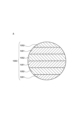
- Fig. 2 is a schematic cross-sectional view showing the configuration of a light-emitting layer 1050 according to one embodiment of the present invention. Specifically, Fig. 2 is a partially enlarged cross-sectional view of region A shown in Fig. 1.
- the light emitting device 1000 includes a ScAlMgO 4 substrate 1011 , an undoped nitride semiconductor layer 1030 , an n-type nitride semiconductor layer 1040 , a light emitting layer 1050 , a p-type nitride semiconductor layer 1060 , a protective layer 1070 , an n-type electrode 1080 , and a p-type electrode 1090 .
- a concave-convex pattern is formed on the first surface 1011_1 of the ScAlMgO 4 substrate 1011.
- the undoped nitride semiconductor layer 1030 is provided on and in contact with the second surface 1011_2 of the ScAlMgO 4 substrate 1011.
- the n-type nitride semiconductor layer 1040 is provided on and in contact with the undoped nitride semiconductor layer 1030.
- the n-type nitride semiconductor layer 1040 has a recess 1041 recessed from the upper surface of the n-type nitride semiconductor.
- the light emitting layer 1050 is provided on and in contact with the n-type nitride semiconductor layer 1040.
- the p-type nitride semiconductor layer 1060 is provided on and in contact with the light emitting layer 1050.
- the protective layer 1070 is provided so as to cover the end face of the undoped nitride semiconductor layer 1030, the end face of the n-type nitride semiconductor layer 1040, the wall and bottom faces of the recess 1041 of the n-type nitride semiconductor layer 1040, the end face of the light emitting layer 1050, and the end face and top face of the p-type nitride semiconductor layer 1060.
- the protective layer 1070 is provided with a first opening 1071 exposing a part of the bottom face of the recess 1041 (i.e., a part of the n-type nitride semiconductor layer 1040 in the recess 1041) and a second opening 1072 exposing a part of the top face of the p-type nitride semiconductor layer 1060.
- the n-type electrode 1080 covers the first opening 1071 and is provided in contact with the n-type nitride semiconductor layer 1040.
- the p-type electrode 1090 covers the second opening 1072 and is provided in contact with the p-type nitride semiconductor layer 1060.
- the ScAlMgO 4 substrate 1011 is a single crystal substrate made of an oxide (ScAlMgO 4 ) containing scandium (Sc), aluminum (Al), and magnesium (Mg).
- the lattice number of ScAlMgO 4 is close to the lattice constant of GaN, and the lattice mismatch is small. Therefore, the GaN film formed on the ScAlMgO 4 substrate 1011 has few defects and is a high-quality film.
- the ScAlMgO 4 substrate is easily lattice-matched with In 0.17 Ga 0.83 N.
- the c-axis of ScAlMgO 4 is oriented along the direction from the first surface 1011_1 to the second surface 1011_2.
- the thickness of the ScAlMgO 4 substrate 1011 is 5 ⁇ m or more and 10 ⁇ m or less. If the thickness of the ScAlMgO 4 substrate 1011 is within this range, the light emitted from the end face of the ScAlMgO 4 substrate 1011 can be reduced, and the extraction efficiency of the light emitted from the first surface 1011_1 of the ScAlMgO 4 substrate 1011 can be improved.
- a concave-convex pattern is formed on the first surface 1011_1 of the ScAlMgO4 substrate 1011. Light emitted from the light emitting layer 1050 is emitted from the first surface 1011_1 of the ScAlMgO4 substrate 1011.
- the concave-convex pattern formed on the first surface 1011_1 can improve the light extraction efficiency.
- the concave-convex height in the concave-convex pattern is 1 ⁇ m or more and 3 ⁇ m or less.
- the undoped nitride semiconductor layer 1030 has a function of improving the crystal quality of the n-type nitride semiconductor layer 1040 formed on the undoped nitride semiconductor layer 1030. It is preferable to use a nitride semiconductor having the same composition as the n-type nitride semiconductor layer 1040 as the undoped nitride semiconductor layer 1030. This reduces the lattice mismatch between the n-type nitride semiconductor layer 1040 and the undoped nitride semiconductor layer 1030, thereby reducing defects in the n-type nitride semiconductor layer formed on the undoped nitride semiconductor layer 1030. For example, In 0.17 Ga 0.83 N can be used as the undoped nitride semiconductor layer 1030.
- the n-type nitride semiconductor layer 1040 has electronic conductivity and has a function of transporting electrons to the light emitting layer 1050.
- the nitride semiconductor contained in the n-type nitride semiconductor layer 1040 is doped with impurities such as silicon (Si) or germanium (Ge). The impurities are activated in the nitride semiconductor to form the n-type nitride semiconductor layer 1040 having electronic conductivity.
- impurities such as silicon (Si) or germanium (Ge).
- the impurities are activated in the nitride semiconductor to form the n-type nitride semiconductor layer 1040 having electronic conductivity.
- In 0.17 Ga 0.83 N doped with Si can be used as the n-type nitride semiconductor layer 1040.
- the thickness of the n-type nitride semiconductor layer 1040 is not particularly limited.
- the thickness of the n-type nitride semiconductor layer 1040 is 500
- the recess 1041 is formed in the n-type nitride semiconductor layer 1040.
- the depth of the recess 1041 is not particularly limited.
- the depth of the recess 1041 is 300 nm or less from the upper surface of the n-type nitride semiconductor layer 1040.
- the light emitting layer 1050 has a function of recombining electrons transported from the n-type nitride semiconductor layer 1040 and holes transported from the p-type nitride semiconductor layer 1060 to emit light. As shown in FIG. 2, the light emitting layer 1050 has a so-called multiple quantum well (MQW) structure in which well layers 1051 and barrier layers 1052 are alternately stacked. A nitride semiconductor is used as each of the well layers 1051 and the barrier layers 1052. For example, In x Ga (1-x) N can be used as the well layer 1051.
- MQW multiple quantum well
- the ratio of In contained in the well layer 1051 is large so that the light emitting device 1000 can emit light in the long wavelength region of the visible light region (for example, yellow or red).
- the value of x is 0.30 or more and 0.50 or less, preferably 0.32 or more and 0.46 or less, more preferably 0.34 or more and 0.42 or less, and particularly preferably 0.36 or more and 0.40 or less.
- the barrier layer 1052 is made of a nitride semiconductor having a band gap larger than that of the nitride semiconductor of the well layer 1051.
- the barrier layer 1052 can be made of In x Ga (1-x) N (0 ⁇ y ⁇ x).
- the p-type nitride semiconductor layer 1060 has hole conductivity and has a function of transporting holes to the light emitting layer 1050. Impurities such as magnesium (Mg) are added to the nitride semiconductor contained in the p-type nitride semiconductor layer 1060. The impurities are activated in the nitride semiconductor to form the p-type nitride semiconductor layer 1060 having hole conductivity. For example, In 0.17 Ga 0.83 N to which Mg is added can be used as the p-type nitride semiconductor layer 1060.
- the thickness of the n-type nitride semiconductor layer 1040 is not particularly limited. For example, the thickness of the p-type nitride semiconductor layer 1060 is 100 nm or more and 500 nm or less.
- the protective layer 1070 prevents impurities (such as moisture) from entering from the outside, and protects the undoped nitride semiconductor layer 1030, the n-type nitride semiconductor layer 1040, the light emitting layer 1050, and the p-type nitride semiconductor layer 1060.
- silicon oxide, silicon nitride, aluminum oxide, or the like can be used as the protective layer 1070.
- the protective layer 1070 may have a single layer structure or a stacked layer structure.
- a laminated film (Al 2 O 3 /SiO 2 ) having an aluminum oxide film on a silicon oxide film can be used as the protective layer 1070.
- the protective layer 1070 may be a silicon nitride (SiN) film.
- n-type electrode 1080 has a function of injecting electrons into the n-type nitride semiconductor layer 1040.
- the n-type electrode 1080 may be a laminate of titanium (Ti), aluminum (Al), and gold (Au) in this order from the bottom.
- the n-type electrode 1080 may have a single layer structure or a multilayer structure.
- the p-type electrode 1090 has a function of injecting holes into the p-type nitride semiconductor layer 1060.
- the p-type electrode 1090 may have a layered structure of nickel (Ni) and gold (Au), or a layered structure of platinum (Pt) and gold (Au).
- a laminated structure of palladium (Pd) and gold (Au) a laminated structure of palladium (Pd) and gold (Au), indium tin oxide (ITO), chromium (Cr), or an alloy thereof can be used. It may have a single layer structure or a laminated structure.
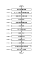
- FIG. 3 is a flow chart illustrating a method for manufacturing the light emitting device 1000 according to one embodiment of the present invention.
- Fig. 4 to Fig. 13 are schematic cross-sectional views illustrating a method for manufacturing the light emitting device 1000 according to one embodiment of the present invention.
- the method for manufacturing the light emitting device 1000 includes steps S1000 to S1120. Steps S1000 to S1120 will be described below in order with reference to FIG. 4 to FIG. 13 as appropriate.
- the degassing prevention layer 1020 is formed on the first surface 1010_1 of the ScAlMgO4 support substrate 1010 (see FIG. 4).
- the ScAlMgO4 substrate 1011 is a part of the ScAlMgO4 support substrate 1010, as will be described in detail later.
- the degassing prevention layer 1020 may be formed, for example, on the first surface 1010_1 of the ScAlMgO4 support substrate 1010 due to contact between the substrate stage and the ScAlMgO4 support substrate 1010 during substrate heating performed in the deposition of the nitride semiconductor film in the manufacturing process of the light emitting device 1000.
- a degassing prevention layer 1020 is formed as a protective film on the first surface 1010_1 of the ScAlMgO4 support substrate 1010. This makes it possible to suppress the occurrence of scratches or chipping of the substrate.
- aluminum nitride is used as the degassing prevention layer 1020.
- the degassing prevention layer 1020 can be formed by chemical vapor deposition (CVD) or sputtering.
- an undoped nitride semiconductor layer 1030 is formed on a second surface 1010_2 opposite to the first surface 1010_1 of the ScAlMgO4 support substrate 1010 (see FIG. 5).
- the undoped nitride semiconductor layer 1030 can be formed by metal-organic chemical vapor deposition (MOCVD) or atomic layer deposition (ALD), for example.
- an n-type nitride semiconductor layer 1040 is formed on the undoped nitride semiconductor layer 1030 (see FIG. 6).
- the n-type nitride semiconductor layer 1040 can be formed by MOCVD, ALD, or the like.
- the light-emitting layer 1050 is formed on the n-type nitride semiconductor layer 1040 (see FIG. 7). Specifically, the nitride semiconductor of the well layer 1051 and the nitride semiconductor of the barrier layer 1052 are alternately formed by sputtering to form the light-emitting layer 1050. In this manner, in this embodiment, the light-emitting layer 1050 is formed by sputtering. Since sputtering can form a film at a lower temperature than MOCVD or ALD, the nitride semiconductor film formed by sputtering can contain a high In composition.
- the nitride semiconductor film formed by sputtering contains a high In composition, phase separation is unlikely to occur in the nitride semiconductor film. Therefore, the nitride semiconductor film of the light-emitting layer 1050 has few crystal defects and is a high-quality film.
- a nitride semiconductor When forming a nitride semiconductor film by sputtering, a nitride semiconductor can be used as the sputtering target, and nitrogen gas or a mixture of nitrogen and argon gas can be used as the sputtering gas.
- the sputtering may be RF sputtering or pulse sputtering.
- a p-type nitride semiconductor layer 1060 is formed on the light-emitting layer 1050 (see FIG. 8).
- the p-type nitride semiconductor layer 1060 can be formed by MOCVD, ALD, or the like.
- a first heat treatment is performed.
- the first heat treatment is mainly for activating the impurities added to the nitride semiconductor of the p-type nitride semiconductor layer 1060.
- the first heat treatment improves the electrical conductivity of the p-type nitride semiconductor layer 1060.
- each layer deposited on the second surface 1010_2 of the ScAlMgO 4 support substrate 1010 is processed into a predetermined pattern shape (see FIG. 9). Specifically, a patterning process is performed by photolithography so that an end face of the undoped nitride semiconductor layer 1030, an end face of the n-type nitride semiconductor layer 1040, an end face of the light emitting layer 1050, and an end face of the p-type nitride semiconductor layer 1060 are exposed. In addition, a recess 1041 in the n-type nitride semiconductor layer 1040 is formed in the patterning process.
- a protective layer 1070 is formed so as to cover the end face of the undoped nitride semiconductor layer 1030, the end face of the n-type nitride semiconductor layer 1040, the wall and bottom faces of the recess 1041 of the n-type nitride semiconductor layer 1040, the end face of the light emitting layer 1050, and the end face and top face of the p-type nitride semiconductor layer 1060 (see FIG. 10).
- the protective layer 1070 can be formed by electron beam evaporation, CVD, sputtering, or the like.
- a first opening 1071 is formed in the protective layer 1070 by photolithography so that the n-type nitride semiconductor layer 1040 is exposed, and a second opening 1072 is formed so that the p-type nitride semiconductor layer 1060 is exposed.
- an n-type electrode 1080 is formed on the n-type nitride semiconductor layer 1040 so as to cover the first opening 1071 (see FIG. 11).
- the n-type electrode 1080 can be formed by sputtering or the like.
- the n-type electrode 1080 is also processed into a predetermined pattern shape by photolithography.
- the n-type electrode 1080 may also be formed using a lift-off method.
- a p-type electrode 1090 is formed on the p-type nitride semiconductor layer 1060 so as to cover the second opening 1072 (see FIG. 12).
- the p-type electrode 1090 can be formed by sputtering or the like.
- the p-type electrode 1090 is also processed into a predetermined pattern shape by photolithography.
- the p-type electrode 1090 may also be formed using a lift-off method.
- steps S1080 and S1090 may be performed in the reverse order, and the n-type electrode 1080 may be formed after the p-type electrode 1090.
- a second heat treatment is performed.
- the second treatment is a heat treatment for improving the interfaces between the n-type nitride semiconductor layer 1040 and the n-type electrode 1080, and between the p-type nitride semiconductor layer 1060 and the p-type electrode 1090.
- the second heat treatment reduces the contact resistance between the n-type nitride semiconductor layer 1040 and the n-type electrode 1080, and between the p-type nitride semiconductor layer 1060 and the p-type electrode 1090.
- step S1110 a cleavage process is performed on the ScAlMgO 4 support substrate 1010 (see FIG. 13).
- step S1110 a cleavage process is performed on the ScAlMgO 4 support substrate 1010 (see FIG. 13).
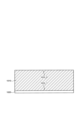
- Fig. 14 is a flow chart for explaining the cleavage process of the ScAlMgO4 support substrate 1010 in the manufacturing method of the light emitting device 1000 according to one embodiment of the present invention.
- Fig. 15 and Fig. 16 are schematic cross-sectional views for explaining the cleavage process of the ScAlMgO4 support substrate 1010 in the manufacturing method of the light emitting device 1000 according to one embodiment of the present invention.
- a notch 1013 is formed on the end surface of the ScAlMgO4 support substrate 1010 (see FIG. 15).
- the notch 1013 is formed by pressing the tip of a diamond pen or a cutter against a predetermined position on the end surface of the ScAlMgO4 support substrate 1010.
- the notch 1013 may be formed by irradiating the end surface of the ScAlMgO4 support substrate 1010 with a laser.
- step S1112 compressive stress is applied to the end face of the ScAlMgO4 support substrate 1010 (FIG. 16).
- ScAlMgO4 has a cleavage plane parallel to the c-axis.
- the c- axis of ScAlMgO4 is oriented along the direction from the first surface 1010_1 to the second surface 1010_2. Therefore, the application of compressive stress causes the ScAlMgO4 support substrate 1010 to be cleaved from the notch 1013.
- each layer on the second surface 1010_2 of the ScAlMgO4 support substrate 1010 can be protected by applying a resist to the second surface 1010_2 side of the ScAlMgO4 support substrate 1010 or by attaching a resist film to form a resist layer.
- the ScAlMgO 4 support substrate 1010 is separated into the ScAlMgO 4 substrate 1011 and the ScAlMgO 4 substrate 1012.
- the ScAlMgO 4 substrate 1011 on which the degassing prevention layer 1020 is formed is removed, and the first surface 1011_1 of the ScAlMgO 4 substrate 1011 appears (the second surface 1011_2 of the ScAlMgO 4 substrate 1011 corresponds to the second surface 1010_2 of the ScAlMgO 4 support substrate 1010).
- the ScAlMgO 4 substrate 1011 on which the degassing prevention layer 1020 is formed can be reused as the ScAlMgO 4 support substrate 1010 for manufacturing another light emitting device 1000.
- step S1120 a concave-convex pattern is formed on the first surface 1011_1 of the ScAlMgO4 substrate 1011.
- the concave-convex pattern is formed by photolithography.
- step S1120 can be performed without peeling off the resist layer in step S1110.
- each layer on the second surface 1011_2 side of the ScAlMgO4 substrate 1011 can be protected in etching the concave-convex pattern.
- ScAlMgO4 can be etched using hydrofluoric acid.
- Al2O3 has high etching resistance to hydrofluoric acid. That is, Al 2 O 3 is difficult to etch with hydrofluoric acid. Therefore, when the protective layer 1070 contains Al 2 O 3 , each layer on the second surface 1011_2 side of the ScAlMgO 4 substrate 1011 can be sufficiently protected.
- the manufacturing method of the light emitting device 1000 has been described based on the flowcharts shown in FIG. 3 and FIG. 14, but the manufacturing method of the light emitting device 1000 is not limited to the steps shown in the flowcharts in FIG. 3 and FIG. 14.
- the light emitting device 1000 may be manufactured using a manufacturing method in which the order of steps S1000 to S1120 is reversed, or may be manufactured using a manufacturing method that includes steps other than steps S1000 to S1120.
- the light emitting layer 1050 but also one or more of the undoped nitride semiconductor layer 1030, the n-type nitride semiconductor layer 1040, and the p-type nitride semiconductor layer 1060 may be formed by sputtering.
- the undoped nitride semiconductor layer 1030, the n-type nitride semiconductor layer 1040, and the p-type nitride semiconductor layer 1060 can be formed at low temperatures, so that the In ratio of the nitride semiconductors contained in the undoped nitride semiconductor layer 1030, the n-type nitride semiconductor layer 1040, and the p-type nitride semiconductor layer 1060 can be increased.
- a buffer layer may be provided on the second surface 1010_2 of the ScAlMgO 4 support substrate 1010.
- the undoped nitride semiconductor layer 1030 includes a nitride semiconductor with a high In ratio formed by sputtering
- the c-axis orientation of the undoped nitride semiconductor layer 1030 can be controlled by providing a buffer layer. Since the undoped nitride semiconductor layer 1030 is provided on the buffer layer, a conductive material or an insulating material may be used as the buffer layer.
- the buffer layer is formed by CVD or sputtering.
- the conductive material of the buffer layer may be titanium (Ti), titanium nitride (TiN x ), titanium oxide (TiO x ), graphene, zinc oxide (ZnO), magnesium diboride (MgB 2 ), aluminum (Al), silver (Ag), calcium (Ca), nickel (Ni), copper (Cu), strontium (Sr), rhodium (Rh), palladium (Pd), cerium (Ce), ytterbium (Yb), iridium (Ir), platinum (Pt), gold (Au), lead (Pb), actinium (Ac), or thorium (Th).
- silicon (Si) or germanium (Ge), or an alloy of these can be used as the conductive material for the buffer layer.
- Silicon and germanium are semiconductor materials, but have higher conductivity than insulating materials, which will be described later. Therefore, in this specification, semiconductor materials such as silicon and germanium used as the buffer layer will be described as conductive materials.
- the insulating material of the buffer layer may be aluminum nitride (AlN), aluminum oxide (Al 2 O 3 ), lithium niobate (LiNbO), BiLaTiO, SrFeO, SrFeO, BiFeO, BaFeO, ZnFeO, PMnN-PZT, or biological apatite (BAp).
- AlN aluminum nitride
- Al 2 O 3 aluminum oxide
- LiNbO lithium niobate
- BiLaTiO BiLaTiO
- SrFeO, SrFeO, BiFeO, BaFeO, ZnFeO, PMnN-PZT or biological apatite
- the light emitting layer 1050 is formed by sputtering, which can be formed at a low temperature, so that phase separation in the nitride semiconductor of the light emitting layer 1050 can be suppressed and the In ratio in the nitride semiconductor can be increased. Therefore, the light emitting device 1000 can emit red light from the light emitting layer 1050 containing a nitride semiconductor. Even when the light emitting device 1000 emits red light, the crystal quality of the light emitting layer 1050 is high, so that the decrease in the light emitting efficiency of the light emitting device 1000 can be suppressed.
- the light emitting device 1000 has improved light extraction efficiency.
- Second Embodiment A light emitting device 1000A according to one embodiment of the present invention will be described with reference to Fig. 17.
- the description of the configuration of the light emitting device 1000A may be omitted.
- FIG. 17 is a schematic cross-sectional view showing the configuration of a light-emitting device 1000A according to one embodiment of the present invention.
- the light emitting device 1000A includes a ScAlMgO 4 substrate 1011, an optical adjustment layer 1100A, an undoped nitride semiconductor layer 1030, an n-type nitride semiconductor layer 1040, a light emitting layer 1050, a p-type nitride semiconductor layer 1060, a protective layer 1070, an n-type electrode 1080, and a p-type electrode 1090.
- the optical adjustment layer 1100A is provided on the first surface 1011_1 of the ScAlMgO 4 substrate 1011.
- the surface of the optical adjustment layer 1100A has an uneven pattern.
- silicon oxide reffractive index 1.46
- polysiloxane reffractive index 1.43
- polysilazane reffractive index 1.55
- the surface of the optical adjustment layer 1100A has an uneven pattern. The uneven pattern can be formed by photolithography after the optical adjustment layer 1100A is formed.
- the optical adjustment layer 1100A is made of a low molecular weight material such as silicon oxide, it can be deposited by CVD or sputtering, or if it is made of a high molecular weight material such as polysiloxane or polysilazane, it can be deposited by coating.
- the optical adjustment layer 1100A has a lower refractive index than the ScAlMgO 4 substrate 1011, and has the function of improving the extraction efficiency of light that passes from the ScAlMgO 4 substrate 1011 through the optical adjustment layer 1100A and is emitted to the outside.
- the light emitted from the light emitting layer 1050 passes through the n-type nitride semiconductor layer 1040, the undoped nitride semiconductor layer 1030, the ScAlMgO 4 substrate 1011, and the optical adjustment layer 1100A and is emitted to the outside.
- the refractive index values of the layers through which the light passes can be decreased in the order of 2.3 (refractive index of the n-type nitride semiconductor layer 1040 and the undoped nitride semiconductor layer 1030), 1.9 (refractive index of the ScAlMgO 4 substrate 1011), and 1.4 to 1.6 (refractive index of the optical adjustment layer 1100A).
- a concavo-convex pattern that improves the light extraction efficiency is formed on the surface of the optical adjustment layer 1100A. Therefore, in the light emitting device 1000A according to this embodiment, the light extraction efficiency is improved.
- the light emitting device 1000B includes a ScAlMgO4 substrate 1011, a glass substrate 1110B, an undoped nitride semiconductor layer 1030, an n-type nitride semiconductor layer 1040, a light emitting layer 1050, a p-type nitride semiconductor layer 1060, a protective layer 1070, an n-type electrode 1080, and a p-type electrode 1090.
- the glass substrate 1110B is provided on the first surface 1011_1 of the ScAlMgO 4 substrate 1011 via an adhesive layer 1120B.
- the adhesive layer 1120B can fix the glass substrate 1110B to the ScAlMgO 4 substrate 1011.
- an acrylic adhesive or an epoxy adhesive can be used as the adhesive layer 1120B.
- An acrylic adhesive or the like is applied to the first surface 1011_1 of the ScAlMgO 4 substrate 1011 exposed by cleavage as shown in FIG. 13, and then the glass substrate 1110B is bonded to the ScAlMgO 4 substrate 1011, thereby manufacturing the light emitting device 1000B.
- the surface of the glass substrate 1110B has an uneven pattern. The uneven pattern may be formed before the glass substrate 1110B is bonded, or may be formed after the glass substrate 1110B is bonded.
- the glass substrate 1110B is amorphous and generally does not have a crystal structure, but a crystal structure may exist in a minute region.
- the upper limit of the thermal expansion coefficient of the glass substrate 1110B is less than 4.2 ⁇ 10 ⁇ 6 /K, preferably less than 4.0 ⁇ 10 ⁇ 6 /K.
- the lower limit of the thermal expansion coefficient of the glass substrate 1110B exceeds 3.0 ⁇ 10 ⁇ 6 /K, preferably exceeds 3.5 ⁇ 10 ⁇ 6 /K.
- the glass substrate 1110B preferably has a low content of alkali metal components in order to prevent contamination of the light-emitting layer 1050.
- the content of alkali metals in the glass substrate 1110B is 0.1 mass % or less.
- an amorphous glass material composed of aluminoborosilicate glass or aluminosilicate glass can be used as the glass substrate 1110B.
- the thickness of the glass substrate 1110B is not particularly limited. However, from the viewpoint of reducing the warpage of the ScAlMgO 4 substrate 1011, it is preferable that the thickness of the glass substrate 1110B is sufficiently larger than the total film thickness of the ScAlMgO 4 substrate 1011, the undoped nitride semiconductor layer 1030, the n-type nitride semiconductor layer 1040, the light emitting layer 1050, and the p-type nitride semiconductor layer 1060.
- the thickness of the glass substrate 1110B is 50 times or more the total film thickness of the undoped nitride semiconductor layer 1030, the n-type nitride semiconductor layer 1040, the light emitting layer 1050, and the p-type nitride semiconductor layer 1060.
- the thickness of the glass substrate 1110B is 0.5 mm or more and 1.0 mm or less.
- the light emitted from the light emitting layer 1050 passes through the n-type nitride semiconductor layer 1040, the undoped nitride semiconductor layer 1030, the ScAlMgO 4 substrate 1011, the adhesive layer 1120B, and 1110B and is emitted to the outside.
- the refractive index values of the layers through which the light passes can be decreased in the order of 2.3 (refractive index of the n-type nitride semiconductor layer 1040 and the undoped nitride semiconductor layer 1030), 1.9 (refractive index of the ScAlMgO 4 substrate 1011), 1.52 to 1.55 (refractive index of the adhesive layer 1120B), and 1.51 (glass substrate 1110B).
- a concave-convex pattern that improves the light extraction efficiency is formed on the surface of the glass substrate 1110B. Therefore, in the light emitting device 1000B according to this embodiment, the light extraction efficiency is improved. In addition, by providing the glass substrate 1110B, the rigidity of the light emitting device 1000B can be increased.
- 1000, 1000A, 1000B Light emitting device, 1010: Support substrate, 1010_1: First surface, 1010_2: Second surface, 1011, 1012: Substrate, 1011_1: First surface, 1011_2: Second surface, 1013: Notch, 1020: Degassing prevention layer, 1030: Undoped nitride semiconductor layer, 1040: n-type nitride semiconductor layer, 1041: Recess, 1050: Light emitting layer, 1051: Well layer, 1052: Barrier layer, 1060: p-type nitride semiconductor layer, 1070: Protective layer, 1071: First opening, 1072: Second opening, 1080: n-type electrode, 1090: p-type electrode, 1100A: optical adjustment layer, 1110B: glass substrate, 1120B: adhesive layer
Landscapes
- Led Devices (AREA)
Abstract
発光装置(1000)は、第1の面(1011_1)および前記第1の面(1011_1)の反対側の第2の面(1011_2)を含むScAlMgO4基板(1011)と、ScAlMgO4基板(1011)の前記第2の面(1011_2)の上のアンドープ窒化物半導体層(1030)と、アンドープ窒化物半導体層(1030)の上の発光層(1050)と、を含み、前記発光層(1050)は、InxGa(1-x)N(0.3≦x≦0.5)を含む井戸層(1051)とInyGa(1-y)N(0<y<x)を含む障壁層(1052)とが交互に積層されたMQW構造を有し、第1の面(1011_1)の側に凹凸パターンが設けられている。
Description
本発明の一実施形態は、窒化物半導体を用いる発光装置に関する。また、本発明の一実施形態は、窒化物半導体を用いる発光装置の製造方法に関する。
GaNおよびInGaNなどの窒化物半導体は、青色発光ダイオードまたは緑色発光ダイオードの多重量子井戸(MQW)構造を有する発光層として広く利用されている。窒化物半導体を赤色発光ダイオードの発光層として利用する場合、窒化物半導体中のIn比率を高くする必要がある。しかしながら、有機金属気相成長(MOCVD)により高温で成膜される窒化物半導体の場合、窒化物半導体中のIn比率を高くすると、相分離が生じ、発光効率が低下する。また、MQW構造においてIn比率が高くなると、井戸層と障壁層との間に格子ひずみによる分極が生じる。その結果、量子閉じ込めシュタルク効果による電流依存性が生じ、発光波長が短波長へシフトする。
近年、窒化物半導体との格子不整合が小さいScAlMgO4基板を用いた発光ダイオードが開発されている(例えば、特許文献1参照)。
しかしながら、ScAlMgO4基板を用いて発光ダイオードを製造する場合であっても、MOCVDにより成膜される窒化物半導体中のIn比率を高くする場合には、窒化物半導体中で相分離してしまい、発光効率が低下してしまうという問題が残る。
本発明の一実施形態は、上記問題に鑑み、発光層の発光効率の低下を抑制し、光取り出し効率を向上した発光装置を提供することを目的の一つとする。また、本発明の一実施形態は、発光層の発光効率の低下を抑制し、光取り出し効率を向上した発光装置の製造方法を提供することを目的の一つとする。
本発明の一実施形態に係る発光装置は、第1の面および前記第1の面の反対側の第2の面を含むScAlMgO4基板と、ScAlMgO4基板の前記第2の面の上のアンドープ窒化物半導体層と、アンドープ窒化物半導体層の上の発光層と、を含み、発光層は、InxGa(1-x)N(0.30≦x≦0.50)を含む井戸層とInyGa(1-y)N(0<y<x)を含む障壁層とが交互に積層されたMQW構造を有し、第1の面の側に凹凸パターンが設けられている。
本発明の一実施形態に係る発光装置の製造方法は、ScAlMgO4支持基板の第1の面の上に、脱ガス防止層を形成し、ScAlMgO4支持基板の第1の面と反対側の第2の面の上に、アンドープ窒化物半導体層を形成し、アンドープ窒化物半導体層の上に、スパッタリングにより、InxGa(1-x)N(0.30≦x≦0.50)を含む井戸層とInyGa(1-y)N(0<y<x)を含む障壁層とを交互に成膜し、MQW構造を有する発光層を形成する、ことを含む。
以下、本発明に係る各実施形態について、図面を参照しつつ説明する。なお、各実施形態はあくまで一例にすぎず、当業者が、発明の主旨を保ちつつ適宜変更することによって容易に想到し得るものについても、当然に本発明の範囲に含まれる。また、図面は、説明をより明確にするため、実際の態様に比べ、各部の幅、厚さ、または形状などが模式的に表される場合がある。しかし、図示された形状などはあくまで一例であって、本発明の解釈を限定するものではない。
本明細書において「αはA、BまたはCを含む」、「αはA、BおよびCのいずれかを含む」、「αはA、BおよびCからなる群から選択される一つを含む」、といった表現は、特に明示が無い限り、αがA~Cの複数の組み合わせを含む場合を排除しない。さらに、これらの表現は、αが他の構成要素を含む場合も排除しない。
本明細書において、説明の便宜上、「上」もしくは「上方」または「下」もしくは「下方」という語句を用いて説明するが、原則として、構造物が形成される基板を基準とし、基板から構造物に向かう方向を「上」または「上方」とする。逆に、構造物から基板に向かう方向を「下」または「下方」とする。したがって、基板上の構造物という表現において、基板と向き合う方向の構造物の面が構造物の下面となり、その反対側の面が構造物の上面となる。また、基板上の構造物という表現においては、基板と構造物との上下関係を説明しているに過ぎず、基板と構造物との間に他の部材が配置されていてもよい。さらに、「上」もしくは「上方」または「下」もしくは「下方」の語句は、複数の層が積層された構造における積層順を意味するものであり、平面視において重畳する位置関係になくてもよい。
本明細書において、構成要素に付記される「第1」、「第2」、または「第3」などの文字は、構成要素を区別するために用いられる便宜的な標識であり、特段の説明がない限り、それ以上の意味を有さない。
本明細書および図面において、同一または類似する複数の構成要素を総じて表記する際には同一の符号を用い、これらの複数の構成要素のそれぞれを区別して表記する際には、大文字のアルファベットを添えて表記する場合がある。また、1つの構成要素のうちの複数の部分を区別して表記する際には、ハイフンと自然数を用いる場合がある。
本明細書において、「膜」という用語と、「層」という用語とは、場合により、互いに入れ替えることができる。
本明細書において、「窒化物半導体」とは、III-V族半導体において、窒素を含む半導体をいう。例えば、「窒化物半導体」は、窒化ガリウム(GaN)または窒化インジウムガリウム(InGaN)などである。
本明細書において、「アンドープ窒化物半導体」とは、不純物が添加されていない窒化物半導体をいう。不純物が添加され、導電性が付与される窒化物半導体は、「p型窒化物半導体」または「n型窒化物半導体」として説明する。
本明細書において、「発光装置」は、発光素子を含むあらゆるデバイスをいう。例えば、「発光装置」には、特定の場所に光を照射する照明装置、および視覚的な画像または映像を表示する表示装置などが含まれる。また、「発光装置」は、発光素子(例えば、LEDチップなど)のみの構成であってもよい。
以下の各実施形態は、技術的な矛盾を生じない限り、互いに組み合わせることができる。
<第1実施形態>
図1~図16を参照して、本発明の一実施形態に係る発光装置1000およびその製造方法について説明する。
図1~図16を参照して、本発明の一実施形態に係る発光装置1000およびその製造方法について説明する。
[1.発光装置1000の構成]
図1は、本発明の一実施形態に係る発光装置1000の構成を示す模式的な断面図である。図2は、本発明の一実施形態に係る発光層1050の構成を示す模式的な断面図である。具体的には、図2は、図1に示す領域Aの部分拡大断面図である。
図1は、本発明の一実施形態に係る発光装置1000の構成を示す模式的な断面図である。図2は、本発明の一実施形態に係る発光層1050の構成を示す模式的な断面図である。具体的には、図2は、図1に示す領域Aの部分拡大断面図である。
図1に示すように、発光装置1000は、ScAlMgO4基板1011、アンドープ窒化物半導体層1030、n型窒化物半導体層1040、発光層1050、p型窒化物半導体層1060、保護層1070、n型電極1080、およびp型電極1090を含む。
ScAlMgO4基板1011の第1の面1011_1には、凹凸パターンが形成されている。アンドープ窒化物半導体層1030は、ScAlMgO4基板1011の第2の面1011_2上に接して設けられている。n型窒化物半導体層1040は、アンドープ窒化物半導体層1030上に接して設けられている。n型窒化物半導体層1040には、n型窒化物半導体の上面から窪んだ凹部1041が形成されている。発光層1050は、n型窒化物半導体層1040上に接して設けられている。p型窒化物半導体層1060は、発光層1050上に接して設けられている。保護層1070は、アンドープ窒化物半導体層1030の端面、n型窒化物半導体層1040の端面、n型窒化物半導体層1040の凹部1041の壁面および底面、発光層1050の端面、ならびにp型窒化物半導体層1060の端面および上面を覆うように設けられている。保護層1070には、凹部1041の底面の一部(すなわち、凹部1041におけるn型窒化物半導体層1040の一部)が露出される第1の開口部1071およびp型窒化物半導体層1060の上面の一部が露出される第2の開口部1072が設けられている。n型電極1080は、第1の開口部1071を覆い、n型窒化物半導体層1040上に接して設けられている。p型電極1090は、第2の開口部1072を覆い、p型窒化物半導体層1060上に接して設けられている。
[1-1.ScAlMgO4基板1011]
ScAlMgO4基板1011は、スカンジウム(Sc)、アルミニウム(Al)、およびマグネシウム(Mg)を含む酸化物(ScAlMgO4)からなる単結晶基板である。ScAlMgO4の格子状数は、GaNの格子定数に近く、格子不整合性が小さい。そのため、ScAlMgO4基板1011上に成膜されるGaN膜は、欠陥が少なく、高品質な膜となる。特に、ScAlMgO4基板は、In0.17Ga0.83Nと格子整合しやすい。ScAlMgO4基板1011では、第1の面1011_1から第2の面1011_2に向かう方向に沿って、ScAlMgO4のc軸が配向している。例えば、ScAlMgO4基板1011の厚さは、5μm以上10μm以下である。ScAlMgO4基板1011の厚さが当該範囲であれば、ScAlMgO4基板1011の端面から出射する光を減らし、ScAlMgO4基板1011の第1の面1011_1から出射する光の取り出し効率を向上させることができる。
ScAlMgO4基板1011は、スカンジウム(Sc)、アルミニウム(Al)、およびマグネシウム(Mg)を含む酸化物(ScAlMgO4)からなる単結晶基板である。ScAlMgO4の格子状数は、GaNの格子定数に近く、格子不整合性が小さい。そのため、ScAlMgO4基板1011上に成膜されるGaN膜は、欠陥が少なく、高品質な膜となる。特に、ScAlMgO4基板は、In0.17Ga0.83Nと格子整合しやすい。ScAlMgO4基板1011では、第1の面1011_1から第2の面1011_2に向かう方向に沿って、ScAlMgO4のc軸が配向している。例えば、ScAlMgO4基板1011の厚さは、5μm以上10μm以下である。ScAlMgO4基板1011の厚さが当該範囲であれば、ScAlMgO4基板1011の端面から出射する光を減らし、ScAlMgO4基板1011の第1の面1011_1から出射する光の取り出し効率を向上させることができる。
ScAlMgO4基板1011の第1の面1011_1には、凹凸パターンが形成されている。発光層1050から出射された光は、ScAlMgO4基板1011の第1の面1011_1から出射される。第1の面1011_1に凹凸パターンが形成されていることにより、光取り出し効率を向上させることができる。例えば、凹凸パターンにおける凹凸高さは、1μm以上3μm以下である。
[1-2.アンドープ窒化物半導体層1030]
アンドープ窒化物半導体層1030は、アンドープ窒化物半導体層1030上に形成されるn型窒化物半導体層1040の結晶品質を向上させる機能を有する。アンドープ窒化物半導体層1030として、n型窒化物半導体層1040と同じ組成の窒化物半導体を用いることが好ましい。これにより、n型窒化物半導体層1040とアンドープ窒化物半導体層1030との格子不整合が小さくなるため、アンドープ窒化物半導体層1030上に形成されるn型窒化物半導体層の欠陥を少なくすることができる。例えば、アンドープ窒化物半導体層1030として、In0.17Ga0.83Nを用いることができる。
アンドープ窒化物半導体層1030は、アンドープ窒化物半導体層1030上に形成されるn型窒化物半導体層1040の結晶品質を向上させる機能を有する。アンドープ窒化物半導体層1030として、n型窒化物半導体層1040と同じ組成の窒化物半導体を用いることが好ましい。これにより、n型窒化物半導体層1040とアンドープ窒化物半導体層1030との格子不整合が小さくなるため、アンドープ窒化物半導体層1030上に形成されるn型窒化物半導体層の欠陥を少なくすることができる。例えば、アンドープ窒化物半導体層1030として、In0.17Ga0.83Nを用いることができる。
[1-3.n型窒化物半導体層1040]
n型窒化物半導体層1040は、電子伝導性を有し、発光層1050に電子を輸送する機能を有する。n型窒化物半導体層1040に含まれる窒化物半導体には、シリコン(Si)またはゲルマニウム(Ge)などの不純物が添加されている。当該不純物が窒化物半導体中で活性化することにより、電子伝導性を有するn型窒化物半導体層1040が形成される。例えば、n型窒化物半導体層1040として、Siが添加されたIn0.17Ga0.83Nを用いることができる。n型窒化物半導体層1040の厚さは、特に限定されない。例えば、n型窒化物半導体層1040の厚さは、500nm以上3000nm以下である。
n型窒化物半導体層1040は、電子伝導性を有し、発光層1050に電子を輸送する機能を有する。n型窒化物半導体層1040に含まれる窒化物半導体には、シリコン(Si)またはゲルマニウム(Ge)などの不純物が添加されている。当該不純物が窒化物半導体中で活性化することにより、電子伝導性を有するn型窒化物半導体層1040が形成される。例えば、n型窒化物半導体層1040として、Siが添加されたIn0.17Ga0.83Nを用いることができる。n型窒化物半導体層1040の厚さは、特に限定されない。例えば、n型窒化物半導体層1040の厚さは、500nm以上3000nm以下である。
上述したように、n型窒化物半導体層1040には、凹部1041が形成されている。凹部1041の深さは、特に限定されない。例えば、凹部1041の深さは、n型窒化物半導体層1040の上面から300nm以下である。
[1-4.発光層1050]
発光層1050は、n型窒化物半導体層1040から輸送された電子とp型窒化物半導体層1060から輸送された正孔とを再結合し、発光する機能を有する。図2に示すように、発光層1050は、井戸層1051と障壁層1052とが交互に積層された、いわゆる多重量子井戸(MQW)構造を有する。井戸層1051および障壁層1052の各々として、窒化物半導体を用いる。例えば、井戸層1051として、InxGa(1-x)Nを用いることができる。本実施形態では、発光装置1000が可視光領域の長波長領域の色(例えば、黄色または赤色)を発光することができるように、井戸層1051に含まれるInの比率が大きい。具体的には、xの値が、0.30以上0.50以下であり、好ましくは0.32以上0.46以下であり、さらに好ましくは0.34以上0.42以下であり、特に好ましくは0.36以上0.40以下である。障壁層1052として、井戸層1051の窒化物半導体よりもバンドギャップの大きな窒化物半導体が用いられる。例えば、障壁層1052として、InxGa(1-x)N(0<y<x)を用いることができる。
発光層1050は、n型窒化物半導体層1040から輸送された電子とp型窒化物半導体層1060から輸送された正孔とを再結合し、発光する機能を有する。図2に示すように、発光層1050は、井戸層1051と障壁層1052とが交互に積層された、いわゆる多重量子井戸(MQW)構造を有する。井戸層1051および障壁層1052の各々として、窒化物半導体を用いる。例えば、井戸層1051として、InxGa(1-x)Nを用いることができる。本実施形態では、発光装置1000が可視光領域の長波長領域の色(例えば、黄色または赤色)を発光することができるように、井戸層1051に含まれるInの比率が大きい。具体的には、xの値が、0.30以上0.50以下であり、好ましくは0.32以上0.46以下であり、さらに好ましくは0.34以上0.42以下であり、特に好ましくは0.36以上0.40以下である。障壁層1052として、井戸層1051の窒化物半導体よりもバンドギャップの大きな窒化物半導体が用いられる。例えば、障壁層1052として、InxGa(1-x)N(0<y<x)を用いることができる。
[1-5.p型窒化物半導体層1060]
p型窒化物半導体層1060は、正孔伝導性を有し、発光層1050に正孔を輸送する機能を有する。p型窒化物半導体層1060に含まれる窒化物半導体には、マグネシウム(Mg)などの不純物が添加されている。当該不純物が窒化物半導体で活性化することにより、正孔伝導性を有するp型窒化物半導体層1060が形成される。例えば、p型窒化物半導体層1060として、Mgが添加されたIn0.17Ga0.83Nを用いることができる。n型窒化物半導体層1040の厚さは、特に限定されない。例えば、p型窒化物半導体層1060の厚さは、100nm以上500nm以下である。
p型窒化物半導体層1060は、正孔伝導性を有し、発光層1050に正孔を輸送する機能を有する。p型窒化物半導体層1060に含まれる窒化物半導体には、マグネシウム(Mg)などの不純物が添加されている。当該不純物が窒化物半導体で活性化することにより、正孔伝導性を有するp型窒化物半導体層1060が形成される。例えば、p型窒化物半導体層1060として、Mgが添加されたIn0.17Ga0.83Nを用いることができる。n型窒化物半導体層1040の厚さは、特に限定されない。例えば、p型窒化物半導体層1060の厚さは、100nm以上500nm以下である。
[1-6.保護層1070]
保護層1070は、外部からの不純物(例えば、水分など)の侵入を抑制し、アンドープ窒化物半導体層1030、n型窒化物半導体層1040、発光層1050、およびp型窒化物半導体層1060を保護する機能を有する。例えば、保護層1070として、酸化シリコン、窒化シリコン、または酸化アルミニウムなどを用いることができる。保護層1070は、単層構造を有していてもよく、積層構造を有していてもよい。例えば、保護層1070が積層構造を有する場合、保護層1070として、酸化シリコン膜の上に酸化アルミニウム膜を有する積層膜(Al2O3/SiO2)を用いることができる。また、保護層1070として、窒化シリコン膜(SiN)を用いてもよい。
保護層1070は、外部からの不純物(例えば、水分など)の侵入を抑制し、アンドープ窒化物半導体層1030、n型窒化物半導体層1040、発光層1050、およびp型窒化物半導体層1060を保護する機能を有する。例えば、保護層1070として、酸化シリコン、窒化シリコン、または酸化アルミニウムなどを用いることができる。保護層1070は、単層構造を有していてもよく、積層構造を有していてもよい。例えば、保護層1070が積層構造を有する場合、保護層1070として、酸化シリコン膜の上に酸化アルミニウム膜を有する積層膜(Al2O3/SiO2)を用いることができる。また、保護層1070として、窒化シリコン膜(SiN)を用いてもよい。
[1-7.n型電極1080]
n型電極1080は、n型窒化物半導体層1040に電子を注入する機能を有する。例えば、n型電極1080として、下から順にチタン(Ti)、アルミニウム(Al)、および金(Au)の積層構造(Au/Al/Ti)、またはこれらの合金などを用いることができる。n型電極1080は、単層構造を有していてもよく、積層構造を有していてもよい。
n型電極1080は、n型窒化物半導体層1040に電子を注入する機能を有する。例えば、n型電極1080として、下から順にチタン(Ti)、アルミニウム(Al)、および金(Au)の積層構造(Au/Al/Ti)、またはこれらの合金などを用いることができる。n型電極1080は、単層構造を有していてもよく、積層構造を有していてもよい。
[1-8.p型電極1090]
p型電極1090は、p型窒化物半導体層1060に正孔を注入する機能を有する。例えば、p型電極1090として、ニッケル(Ni)および金(Au)の積層構造、白金(Pt)および金(Au)の積層構造、パラジウム(Pd)および金(Au)の積層構造、酸化インジウムスズ(ITO)、もしくはクロム(Cr)、またはこれらの合金などを用いることができる。p型電極1090は、単層構造を有していてもよく、積層構造を有していてもよい。
p型電極1090は、p型窒化物半導体層1060に正孔を注入する機能を有する。例えば、p型電極1090として、ニッケル(Ni)および金(Au)の積層構造、白金(Pt)および金(Au)の積層構造、パラジウム(Pd)および金(Au)の積層構造、酸化インジウムスズ(ITO)、もしくはクロム(Cr)、またはこれらの合金などを用いることができる。p型電極1090は、単層構造を有していてもよく、積層構造を有していてもよい。
[2.発光装置1000の製造方法]
図3は、本発明の一実施形態に係る発光装置1000の製造方法を説明するフローチャートである。図4~図13は、本発明の一実施形態に係る発光装置1000の製造方法を説明する模式的な断面図である。
図3は、本発明の一実施形態に係る発光装置1000の製造方法を説明するフローチャートである。図4~図13は、本発明の一実施形態に係る発光装置1000の製造方法を説明する模式的な断面図である。
図3に示すように、発光装置1000の製造方法は、ステップS1000~ステップS1120を含む。以下、適宜、図4~図13を参照しながら、ステップS1000~ステップS1120を順に説明する。
ステップS1000では、ScAlMgO4支持基板1010の第1の面1010_1上に、脱ガス防止層1020を成膜する(図4参照)。詳細は後述するが、ScAlMgO4基板1011は、ScAlMgO4支持基板1010の一部である。脱ガス防止層1020は、発光装置1000の製造工程の窒化物半導体膜の成膜において行われる基板加熱の際に、基板ステージとScAlMgO4支持基板1010との接触により、例えば、ScAlMgO4支持基板1010の第1の面1010_1に傷または欠けなどが形成される場合がある。この場合、傷または欠けから、ScAlMgO4支持基板1010中のMgが抜け、成膜中の窒化物半導体膜に、不純物としてMgが混入する。そのため、Mgが抜けることを防止するため、ScAlMgO4支持基板1010の第1の面1010_1に保護膜としての脱ガス防止層1020を形成する。これにより、基板の傷または欠けの発生を抑制することができる。例えば、脱ガス防止層1020として、窒化アルミニウムなどが用いられる。脱ガス防止層1020は、化学気相成長(CVD)またはスパッタリングなどにより成膜することができる。
ステップS1010では、ScAlMgO4支持基板1010の第1の面1010_1と反対側の第2の面1010_2上に、アンドープ窒化物半導体層1030を成膜する(図5参照)。アンドープ窒化物半導体層1030は、有機金属気相成長(MOCVD)または原子堆積(ALD)などにより成膜することができる。
ステップS1020では、アンドープ窒化物半導体層1030上に、n型窒化物半導体層1040を成膜する(図6参照)。n型窒化物半導体層1040は、MOCVDまたはALDなどにより成膜することができる。
ステップS1030では、n型窒化物半導体層1040上に、発光層1050を形成する(図7参照)。具体的には、井戸層1051の窒化物半導体と障壁層1052の窒化物半導体とをスパッタリングにより交互に成膜し、発光層1050を形成する。このように、本実施形態では、スパッタリングにより発光層1050が形成される。スパッタリングは、MOCVDまたはALDよりも低温で成膜することができるため、スパッタリングにより成膜される窒化物半導体膜は、高いIn組成を含むことが可能である。換言すると、スパッタリングにより成膜される窒化物半導体膜は、高いIn組成を含む場合であっても、窒化物半導体膜中で相分離が生じにくい。そのため、発光層1050の窒化物半導体膜は、結晶欠陥が少なく、高品質な膜となる。
スパッタリングによる窒化物半導体膜の成膜においては、スパッタリングターゲットとして窒化物半導体を用い、スパッタリングガスとして窒素ガスまたは窒素とアルゴンの混合ガスを用いることができる。スパッタリングは、RFスパッタリングであってもよく、パルススパッタリングであってもよい。
ステップS1040では、発光層1050上に、p型窒化物半導体層1060を成膜する(図8参照)。p型窒化物半導体層1060は、MOCVDまたはALDなどにより成膜することができる。
ステップS1050では、第1の熱処理が行われる。第1の熱処理は、主に、p型窒化物半導体層1060の窒化物半導体に添加された不純物を活性化させるための熱処理である。第1の熱処理により、p型窒化物半導体層1060の導電性が向上する。
ステップS1060では、ScAlMgO4支持基板1010の第2の面1010_2上に成膜された各層を所定のパターン形状に加工する(図9参照)。具体的には、アンドープ窒化物半導体層1030の端面、n型窒化物半導体層1040の端面、発光層1050の端面、およびp型窒化物半導体層1060の端面が露出されるように、フォトリソグラフィによるパターニング加工が行われる。また、パターニング加工において、n型窒化物半導体層1040の凹部1041が形成される。
ステップS1070では、アンドープ窒化物半導体層1030の端面、n型窒化物半導体層1040の端面、n型窒化物半導体層1040の凹部1041の壁面および底面、発光層1050の端面、ならびにp型窒化物半導体層1060の端面および上面を覆うように、保護層1070が形成される(図10参照)。保護層1070は、電子ビーム蒸着、CVD、またはスパッタリングなどにより成膜することができる。また、保護層1070には、フォトリソグラフィにより、n型窒化物半導体層1040が露出されるように第1の開口部1071が形成され、p型窒化物半導体層1060が露出されるように第2の開口部1072が形成される。
ステップS1080では、第1の開口部1071を覆うように、n型窒化物半導体層1040上にn型電極1080が形成される(図11参照)。n型電極1080は、スパッタリングなどにより成膜することができる。また、n型電極1080は、フォトリソグラフィにより所定のパターン形状に加工される。また、n型電極1080は、リフトオフ法を用いて形成されてもよい。
ステップS1090では、第2の開口部1072を覆うように、p型窒化物半導体層1060上にp型電極1090が形成される(図12参照)。p型電極1090は、スパッタリングなどにより成膜することができる。また、p型電極1090は、フォトリソグラフィにより所定のパターン形状に加工される。また、p型電極1090は、リフトオフ法を用いて形成されてもよい。
なお、ステップS1080とステップS1090については逆の順序で行われるものであってもよく、p型電極1090形成後にn型電極1080を形成するものであっても良い。
ステップS1100では、第2の熱処理が行われる。第2の処理は、主に、n型窒化物半導体層1040とn型電極1080との間、およびp型窒化物半導体層1060とp型電極1090との間の界面を改善するための熱処理である。第2の熱処理により、n型窒化物半導体層1040とn型電極1080との間、およびp型窒化物半導体層1060とp型電極1090との間のコンタクト抵抗が低下する。
ステップS1110では、ScAlMgO4支持基板1010の劈開処理が行われる(図13参照)。ここで、図14~図16を参照して、ステップS1110の詳細について説明する。
図14は、本発明の一実施形態に係る発光装置1000の製造方法において、ScAlMgO4支持基板1010の劈開処理を説明するフローチャートである。図15および図16は、本発明の一実施形態に係る発光装置1000の製造方法において、ScAlMgO4支持基板1010の劈開処理を説明する模式的な断面図である。
ステップS1111では、ScAlMgO4支持基板1010の端面に切欠部1013を形成する(図15参照)。切欠部1013は、ScAlMgO4支持基板1010の端面の所定の位置にダイヤモンドペンまたはカッターなどの先端を押し当てることにより形成される。また、ScAlMgO4支持基板1010の端面にレーザを照射し、切欠部1013を形成してもよい。
ステップS1112では、ScAlMgO4支持基板1010の端面に圧縮応力を印加する(図16)。ScAlMgO4は、c軸と平行に劈開面を有する。ScAlMgO4支持基板1010では、第1の面1010_1から第2の面1010_2に向かう方向に沿って、ScAlMgO4のc軸が配向している。そのため、圧縮応力の印加により、ScAlMgO4支持基板1010は切欠部1013から劈開される。
ScAlMgO4支持基板1010の劈開処理では、切欠部1013の形成およびScAlMgO4の劈開において、パーティクルが発生する場合がある。そのため、ScAlMgO4支持基板1010の第2の面1010_2側が保護されていることが好ましい。例えば、ScAlMgO4支持基板1010の第2の面1010_2側に、レジストを塗布し、またはレジストフィルムを貼付してレジスト層を形成することにより、ScAlMgO4支持基板1010の第2の面1010_2上の各層を保護することができる。
以上説明したScAlMgO4支持基板1010の劈開処理により、図13に示すように、ScAlMgO4支持基板1010は、ScAlMgO4基板1011とScAlMgO4基板1012とに分離される。脱ガス防止層1020が形成されたScAlMgO4基板1011は除去され、ScAlMgO4基板1011の第1の面1011_1が現れる(ScAlMgO4基板1011の第2の面1011_2は、ScAlMgO4支持基板1010の第2の面1010_2に対応する。)。なお、脱ガス防止層1020が形成されたScAlMgO4基板1011は、別の発光装置1000を製造するためのScAlMgO4支持基板1010として再利用することができる。
ステップS1120では、ScAlMgO4基板1011の第1の面1011_1に、凹凸パターンを形成する。凹凸パターンは、フォトリソグラフィにより形成される。ScAlMgO4支持基板1010の劈開処理において、ScAlMgO4基板1011の第2の面1011_2側にレジスト層が形成されている場合、ステップS1110においてレジスト層を剥離することなく、ステップS1120を行うことができる。ScAlMgO4基板1011の第2の面1011_2側にレジスト層が形成されていると、凹凸パターンのエッチングにおいて、ScAlMgO4基板1011の第2の面1011_2側の各層を保護することができる。ScAlMgO4は、フッ酸を用いてエッチングすることができる。Al2O3は、フッ酸に対するエッチング耐性が高い。すなわち、Al2O3は、フッ酸によってエッチングされにくい。そのため、保護層1070にAl2O3が含まれていると、ScAlMgO4基板1011の第2の面1011_2側の各層を十分に保護することができる。
図3および図14に示すフローチャートに基づき、発光装置1000の製造方法について説明したが、発光装置1000の製造方法は、図3および図14のフローチャートに示すステップに限られない。発光装置1000は、ステップS1000~ステップS1120の順序が入れ替えられた製造方法を用いて製造されてもよく、ステップS1000~ステップS1120以外のステップが含まれた製造方法を用いて製造されてもよい。
なお、説明を省略するが、発光層1050だけでなく、アンドープ窒化物半導体層1030、n型窒化物半導体層1040、およびp型窒化物半導体層1060のいずれか1つまたは複数は、スパッタリングにより成膜されてもよい。この場合、アンドープ窒化物半導体層1030、n型窒化物半導体層1040、およびp型窒化物半導体層1060を低温で成膜することができるため、アンドープ窒化物半導体層1030、n型窒化物半導体層1040、およびp型窒化物半導体層1060に含まれる窒化物半導体のIn比率を高めることができる。
また、図示しないが、ScAlMgO4支持基板1010の第2の面1010_2上には、バッファー層が設けられてもよい。アンドープ窒化物半導体層1030がスパッタリングで成膜されるIn比率が高い窒化物半導体を含む場合、バッファー層を設けられることにより、アンドープ窒化物半導体層1030のc軸配向性を制御することができる。バッファー層上にはアンドープ窒化物半導体層1030が設けられるため、バッファー層として、導電性材料が用いられてもよく、絶縁性材料が用いられてもよい。バッファー層は、CVDまたはスパッタリングにより成膜される。
例えば、バッファー層の導電性材料として、チタン(Ti)、窒化チタン(TiNx)、酸化チタン(TiOx)、グラフェン、酸化亜鉛(ZnO)、二ホウ化マグネシウム(MgB2)、アルミニウム(Al)、銀(Ag)、カルシウム(Ca)、ニッケル(Ni)、銅(Cu)、ストロンチウム(Sr)、ロジウム(Rh)、パラジウム(Pd)、セリウム(Ce)、イッテルビウム(Yb)、イリジウム(Ir)、白金(Pt)、金(Au)、鉛(Pb)、アクチニウム(Ac)、またはトリウム(Th)などを用いることができる。特に、バッファー層の材料として、Ti、グラフェン、またはZnOが用いられることが好ましい。
また、バッファー層の導電性材料として、シリコン(Si)もしくはゲルマニウム(Ge)、またはこれらの合金などを用いることもできる。シリコンおよびゲルマニウムは、半導体材料であるが、後述する絶縁性材料よりは高い導電性を有する。そのため、本明細書では、バッファー層として用いられるシリコンおよびゲルマニウムなどの半導体材料は、導電性材料として説明する。
また、例えば、バッファー層の絶縁性材料として、窒化アルミニウム(AlN)、酸化アルミニウム(Al2O3)、ニオブ酸リチウム(LiNbO)、BiLaTiO、SrFeO、SrFeO、BiFeO、BaFeO、ZnFeO、PMnN-PZT、または生体アパタイト(BAp)などを用いることができる。特に、バッファー層として、AlNを用いることが好ましい。
本実施形態では、低温で成膜可能なスパッタリングにより発光層1050を形成するため、発光層1050の窒化物半導体中の相分離を抑制し、窒化物半導体中のIn比率を高めることができる。そのため、発光装置1000は、窒化物半導体を含む発光層1050から赤色の発光が可能である。また、発光装置1000が赤色に発光する場合であっても、発光層1050の結晶品質が高いため、発光装置1000の発光効率の低下を抑制することができる。さらに、発光装置1000から光が出射されるScAlMgO4基板1011の第1の面1011_1に、光取り出し効率を向上させる凹凸パターンが形成されている。そのため、本実施形態に係る発光装置1000は、光取り出し効率が向上する。
<第2実施形態>
図17を参照して、本発明の一実施形態に係る発光装置1000Aについて説明する。なお、以下では、発光装置1000Aの構成が発光装置1000の構成と同様であるとき、発光装置1000Aの構成の説明を省略する場合がある。
図17を参照して、本発明の一実施形態に係る発光装置1000Aについて説明する。なお、以下では、発光装置1000Aの構成が発光装置1000の構成と同様であるとき、発光装置1000Aの構成の説明を省略する場合がある。
図17は、本発明の一実施形態に係る発光装置1000Aの構成を示す模式的な断面図である。
図17に示すように、発光装置1000Aは、ScAlMgO4基板1011、光学調整層1100A、アンドープ窒化物半導体層1030、n型窒化物半導体層1040、発光層1050、p型窒化物半導体層1060、保護層1070、n型電極1080、およびp型電極1090を含む。
光学調整層1100Aは、ScAlMgO4基板1011の第1の面1011_1に設けられている。光学調整層1100Aの表面は、凹凸パターンを有する。例えば、光学調整層1100Aとして、酸化シリコン(屈折率1.46)、ポリシロキサン(屈折率1.43)、またはポリシラザン(屈折率1.55)などを用いることができる。なお、光学調整層1100Aの表面は、凹凸パターンを有する。凹凸パターンは、光学調整層1100Aが成膜された後において、フォトリソグラフィにより形成することができる。
光学調整層1100Aは、酸化シリコンなどの低分子材料であれば、CVDまたはスパッタなどにより成膜することができ、ポリシロキサンまたはポリシラザンなどの高分子材料であれば、塗布などにより成膜することができる。
光学調整層1100Aは、ScAlMgO4基板1011よりも低い屈折率を有し、ScAlMgO4基板1011から光学調整層1100Aを通過して外部に出射される光の取出し効率を向上させる機能を有する。
本実施形態では、発光層1050から出射された光は、n型窒化物半導体層1040、アンドープ窒化物半導体層1030、ScAlMgO4基板1011、および光学調整層1100Aを通過して外部に出射される。光が通過する層の屈折率の値は、概ね、2.3(n型窒化物半導体層1040およびアンドープ窒化物半導体層1030の屈折率)、1.9(ScAlMgO4基板1011の屈折率)、および1.4~1.6(光学調整層1100Aの屈折率)の順に小さくすることが可能である。また、光学調整層1100Aの表面には、光取り出し効率を向上させる凹凸パターンが形成されている。そのため、本実施形態に係る発光装置1000Aでは、光取り出し効率が向上する。
<第3実施形態>
図18を参照して、本発明の一実施形態に係る発光装置1000Bについて説明する。なお、以下では、発光装置1000Bの構成が発光装置1000の構成と同様であるとき、発光装置1000Bの構成の説明を省略する場合がある。
図18を参照して、本発明の一実施形態に係る発光装置1000Bについて説明する。なお、以下では、発光装置1000Bの構成が発光装置1000の構成と同様であるとき、発光装置1000Bの構成の説明を省略する場合がある。
図18に示すように、発光装置1000Bは、ScAlMgO4基板1011、ガラス基板1110B、アンドープ窒化物半導体層1030、n型窒化物半導体層1040、発光層1050、p型窒化物半導体層1060、保護層1070、n型電極1080、およびp型電極1090を含む。
ガラス基板1110Bは、ScAlMgO4基板1011の第1の面1011_1に、接着層1120Bを介して設けられている。接着層1120Bは、ガラス基板1110BをScAlMgO4基板1011に固定することができる。例えば、接着層1120Bとして、アクリル接着剤またはエポキシ接着剤などを用いることができる。図13に示す劈開されて露出されScAlMgO4基板1011の第1の面1011_1上にアクリル接着剤などが塗布され、その後、ガラス基板1110Bを貼り合わせることにより、発光装置1000Bを製造することができる。なお、ガラス基板1110Bの表面は、凹凸パターンを有する。凹凸パターンは、ガラス基板1110Bが接着される前に形成されていてもよく、ガラス基板1110Bが接着された後に形成されてもよい。
ガラス基板1110Bは、概ね結晶構造を有しない非晶質であるが、微小領域においては結晶構造が存在してもよい。ガラス基板1110Bの熱膨張係数の上限は、4.2×10⁻⁶/K未満、好ましくは4.0×10-6/K未満である。ガラス基板1110Bの熱膨張係数の下限は、3.0×10-6/Kを超え、好ましくは3.5×10-6/Kを超える。ガラス基板1110Bは、発光層1050への汚染を防止するため、アルカリ金属成分の含有量が少ないことが好ましい。例えば、ガラス基板1110B中のアルカリ金属の含有量は0.1質量%以下である。例えば、ガラス基板1110Bとして、アルミノホウケイ酸ガラスまたはアルミノシリケートガラスで構成される非晶質ガラス材料を用いることができる。
ガラス基板1110Bの厚さは、特に限定されない。但し、ScAlMgO4基板1011の反りを低減する観点から、ガラス基板1110Bの厚さは、ScAlMgO4基板1011、アンドープ窒化物半導体層1030、n型窒化物半導体層1040、発光層1050、およびp型窒化物半導体層1060の総膜厚よりも十分に大きいことが好ましい。例えば、ガラス基板1110Bの厚さは、アンドープ窒化物半導体層1030、n型窒化物半導体層1040、発光層1050、およびp型窒化物半導体層1060の総膜厚の50倍以上である。具体的には、ガラス基板1110Bの厚さは、0.5mm以上1.0mm以下である。
本実施形態では、発光層1050から出射された光は、n型窒化物半導体層1040、アンドープ窒化物半導体層1030、ScAlMgO4基板1011、接着層1120B、および1110Bを通過して外部に出射される。光が通過する層の屈折率の値は、概ね、2.3(n型窒化物半導体層1040およびアンドープ窒化物半導体層1030の屈折率)、1.9(ScAlMgO4基板1011の屈折率)、1.52~1.55(接着層1120Bの屈折率)、および1.51(ガラス基板1110B)の順に小さくすることが可能である。また、ガラス基板1110Bの表面には、光取り出し効率を向上させる凹凸パターンが形成されている。そのため、本実施形態に係る発光装置1000Bでは、光取り出し効率が向上する。また、ガラス基板1110Bを設けることにより、発光装置1000Bの剛性を高めることができる。
本発明の実施形態として上述した各実施形態は、相互に矛盾しない限りにおいて、適宜組み合わせて実施することができる。また、各実施形態を基にして、当業者が適宜構成要素の追加、削除、もしくは設計変更を行ったもの、または工程の追加、省略、もしくは条件変更を行ったものも、本発明の要旨を備えている限り、本発明の範囲に含まれる。
上述した各実施形態によりもたらされる作用効果とは異なる他の作用効果であっても、本明細書の記載から明らかなもの、または、当業者において容易に予測し得るものについては、当然に本発明によりもたらされるものと解される。
1000、1000A、1000B:発光装置、 1010:支持基板、 1010_1:第1の面、 1010_2:第2の面、 1011、1012:基板、 1011_1:第1の面、 1011_2:第2の面、 1013:切欠部、 1020:脱ガス防止層、 1030:アンドープ窒化物半導体層、 1040:n型窒化物半導体層、 1041:凹部、 1050:発光層、 1051:井戸層、 1052:障壁層、 1060:p型窒化物半導体層、 1070:保護層、 1071:第1の開口部、 1072:第2の開口部、 1080:n型電極、 1090:p型電極、 1100A:光学調整層、 1110B:ガラス基板、 1120B:接着層
Claims (16)
- 第1の面および前記第1の面の反対側の第2の面を含むScAlMgO4基板と、
前記ScAlMgO4基板の前記第2の面の上のアンドープ窒化物半導体層と、
前記アンドープ窒化物半導体層の上の発光層と、を含み、
前記発光層は、InxGa(1-x)N(0.30≦x≦0.50)を含む井戸層とInyGa(1-y)N(0<y<x)を含む障壁層とが交互に積層されたMQW構造を有し、
前記第1の面の側に凹凸パターンが設けられている、発光装置。 - 前記アンドープ窒化物半導体層は、前記ScAlMgO4基板の前記第2の面と接している、請求項1に記載の発光装置。
- 前記凹凸パターンにおける凹凸高さは、1μm以上3μm以下である、請求項1に記載の発光装置。
- 前記ScAlMgO4基板の厚さは、5μm以上10μm以下である、請求項1に記載の発光装置。
- 前記凹凸パターンは、前記ScAlMgO4基板の前記第1の面に形成されている、請求項1に記載の発光装置。
- さらに、前記ScAlMgO4基板の前記第1の面の上の光学調整層を含み、
前記光学調整層の屈折率は、前記ScAlMgO4基板の屈折率よりも小さく、
前記凹凸パターンは、前記光学調整層に形成されている、請求項1に記載の発光装置。 - さらに、前記ScAlMgO4基板の前記第1の面に接着されたガラス基板を含み、
前記凹凸パターンは、前記ガラス基板に形成されている、請求項1に記載の発光装置。 - ScAlMgO4支持基板の第1の面の上に、脱ガス防止層を形成し、
前記ScAlMgO4支持基板の前記第1の面と反対側の第2の面の上に、アンドープ窒化物半導体層を形成し、
前記アンドープ窒化物半導体層の上に、スパッタリングにより、InxGa(1-x)N(0.30≦x≦0.50)を含む井戸層とInyGa(1-y)N(0<y<x)を含む障壁層とを交互に成膜し、MQW構造を有する発光層を形成する、ことを含む、発光装置の製造方法。 - 前記アンドープ窒化物半導体層は、スパッタリングにより成膜される、請求項8に記載の発光装置の製造方法。
- さらに、前記ScAlMgO4支持基板を劈開して、前記脱ガス防止層を除去する、ことを含む、請求項8に記載の発光装置の製造方法。
- さらに、前記ScAlMgO4支持基板が劈開されて現れた第3の面に、凹凸パターンを形成する、ことを含む、請求項10に記載の発光装置の製造方法。
- さらに、前記ScAlMgO4支持基板が劈開されて現れた第3の面に、光学調整層を形成する、ことを含み、
前記光学調整層の屈折率は、前記ScAlMgO4基板の屈折率よりも小さい、請求項10に記載の発光装置の製造方法。 - さらに、前記光学調整層に、凹凸パターンを形成する、ことを含む、請求項12に記載の発光装置の製造方法。
- さらに、前記ScAlMgO4支持基板が劈開されて現れた第3の面に、ガラス基板を接着する、ことを含む、請求項10に記載の発光装置の製造方法。
- 前記第3の面に接着される前の前記ガラス基板は、凹凸パターンを含む、請求項14に記載の発光装置の製造方法。
- 前記ScAlMgO4支持基板の劈開は、
前記ScAlMgO4支持基板の端面に切欠部を形成し、
前記ScAlMgO4支持基板の前記端面に圧縮圧力を印加する、ことを含む、請求項10に記載の発光装置の製造方法。
Priority Applications (1)
| Application Number | Priority Date | Filing Date | Title |
|---|---|---|---|
| US19/413,075 US20260096250A1 (en) | 2023-07-03 | 2025-12-09 | Light emitting device and manufacturing method thereof |
Applications Claiming Priority (2)
| Application Number | Priority Date | Filing Date | Title |
|---|---|---|---|
| JP2023-109627 | 2023-07-03 | ||
| JP2023109627 | 2023-07-03 |
Related Child Applications (1)
| Application Number | Title | Priority Date | Filing Date |
|---|---|---|---|
| US19/413,075 Continuation US20260096250A1 (en) | 2023-07-03 | 2025-12-09 | Light emitting device and manufacturing method thereof |
Publications (1)
| Publication Number | Publication Date |
|---|---|
| WO2025009271A1 true WO2025009271A1 (ja) | 2025-01-09 |
Family
ID=94171818
Family Applications (1)
| Application Number | Title | Priority Date | Filing Date |
|---|---|---|---|
| PCT/JP2024/017972 Ceased WO2025009271A1 (ja) | 2023-07-03 | 2024-05-15 | 発光装置およびその製造方法 |
Country Status (2)
| Country | Link |
|---|---|
| US (1) | US20260096250A1 (ja) |
| WO (1) | WO2025009271A1 (ja) |
Citations (6)
| Publication number | Priority date | Publication date | Assignee | Title |
|---|---|---|---|---|
| JP2007329312A (ja) * | 2006-06-08 | 2007-12-20 | Showa Denko Kk | Iii族窒化物半導体積層構造体の製造方法 |
| JP2008091855A (ja) * | 2006-09-06 | 2008-04-17 | Toshiba Lighting & Technology Corp | 照明装置 |
| JP2017168783A (ja) * | 2016-03-18 | 2017-09-21 | 国立大学法人東北大学 | 半導体装置およびその製造方法 |
| JP2018197179A (ja) * | 2017-05-24 | 2018-12-13 | パナソニック株式会社 | Ramo4基板及び窒化物半導体装置 |
| JP2020009914A (ja) * | 2018-07-09 | 2020-01-16 | パナソニック株式会社 | Iii族窒化物半導体発光ダイオード、およびその製造方法 |
| JP2022049620A (ja) * | 2020-09-16 | 2022-03-29 | アルディーテック株式会社 | 半導体発光素子チップ集積装置およびその製造方法 |
-
2024
- 2024-05-15 WO PCT/JP2024/017972 patent/WO2025009271A1/ja not_active Ceased
-
2025
- 2025-12-09 US US19/413,075 patent/US20260096250A1/en active Pending
Patent Citations (6)
| Publication number | Priority date | Publication date | Assignee | Title |
|---|---|---|---|---|
| JP2007329312A (ja) * | 2006-06-08 | 2007-12-20 | Showa Denko Kk | Iii族窒化物半導体積層構造体の製造方法 |
| JP2008091855A (ja) * | 2006-09-06 | 2008-04-17 | Toshiba Lighting & Technology Corp | 照明装置 |
| JP2017168783A (ja) * | 2016-03-18 | 2017-09-21 | 国立大学法人東北大学 | 半導体装置およびその製造方法 |
| JP2018197179A (ja) * | 2017-05-24 | 2018-12-13 | パナソニック株式会社 | Ramo4基板及び窒化物半導体装置 |
| JP2020009914A (ja) * | 2018-07-09 | 2020-01-16 | パナソニック株式会社 | Iii族窒化物半導体発光ダイオード、およびその製造方法 |
| JP2022049620A (ja) * | 2020-09-16 | 2022-03-29 | アルディーテック株式会社 | 半導体発光素子チップ集積装置およびその製造方法 |
Also Published As
| Publication number | Publication date |
|---|---|
| US20260096250A1 (en) | 2026-04-02 |
Similar Documents
| Publication | Publication Date | Title |
|---|---|---|
| JP5251121B2 (ja) | 窒化ガリウム系半導体発光素子及びその製造方法 | |
| CN100561758C (zh) | 氮化镓化合物半导体发光元件及其制造方法 | |
| JP6419077B2 (ja) | 波長変換発光デバイス | |
| US8022430B2 (en) | Nitride-based compound semiconductor light-emitting device | |
| CN101512783A (zh) | 半导体发光元件 | |
| WO2010050410A1 (ja) | 半導体発光素子の製造方法 | |
| US8390007B2 (en) | Semiconductor light emitting device and method of fabricating semiconductor light emitting device | |
| WO2010150501A1 (ja) | 発光素子、その製造方法、ランプ、電子機器及び機械装置 | |
| KR20080070696A (ko) | 질화물 반도체 발광소자 | |
| JP2008294188A (ja) | 半導体発光素子及びその製造方法 | |
| CN110223999A (zh) | 半导体发光装置及其制造方法 | |
| WO2016051908A1 (ja) | 発光素子および発光素子の製造方法 | |
| JP2011009386A (ja) | Iii族窒化物半導体発光素子およびその製造方法 | |
| US20240136469A1 (en) | Light-emitting element and manufacturing method thereof | |
| JP2009231549A (ja) | 窒化物系半導体発光素子 | |
| US20260047237A1 (en) | Nitride semiconductor device and method for manufacturing nitride semiconductor device | |
| TW201031013A (en) | Optical device and the forming method thereof | |
| JP2008277323A (ja) | 半導体発光素子およびウエハ | |
| JP7737020B2 (ja) | 垂直共振器面発光レーザ素子の製造方法及び垂直共振器面発光レーザ素子 | |
| CN115458652A (zh) | 高亮发光二极管及其制备方法 | |
| JP5945409B2 (ja) | 半導体素子とその製造方法 | |
| WO2025009271A1 (ja) | 発光装置およびその製造方法 | |
| KR101499954B1 (ko) | 수직구조 그룹 3족 질화물계 반도체 발광다이오드 소자 및제조방법 | |
| JP2011159801A (ja) | 半導体発光素子及びその製造方法、並びにランプ | |
| JP2008016629A (ja) | 3族窒化物系発光ダイオード素子の製造方法 |
Legal Events
| Date | Code | Title | Description |
|---|---|---|---|
| NENP | Non-entry into the national phase |
Ref country code: DE |